WO2015174188A1 - 光発電装置 - Google Patents
光発電装置 Download PDFInfo
- Publication number
- WO2015174188A1 WO2015174188A1 PCT/JP2015/061449 JP2015061449W WO2015174188A1 WO 2015174188 A1 WO2015174188 A1 WO 2015174188A1 JP 2015061449 W JP2015061449 W JP 2015061449W WO 2015174188 A1 WO2015174188 A1 WO 2015174188A1
- Authority
- WO
- WIPO (PCT)
- Prior art keywords
- operating point
- photovoltaic
- dsc
- operating
- voltage
- Prior art date
- Legal status (The legal status is an assumption and is not a legal conclusion. Google has not performed a legal analysis and makes no representation as to the accuracy of the status listed.)
- Ceased
Links
Images


Classifications
-
- H—ELECTRICITY
- H01—ELECTRIC ELEMENTS
- H01G—CAPACITORS; CAPACITORS, RECTIFIERS, DETECTORS, SWITCHING DEVICES, LIGHT-SENSITIVE OR TEMPERATURE-SENSITIVE DEVICES OF THE ELECTROLYTIC TYPE
- H01G9/00—Electrolytic capacitors, rectifiers, detectors, switching devices, light-sensitive or temperature-sensitive devices; Processes of their manufacture
- H01G9/20—Light-sensitive devices
- H01G9/2068—Panels or arrays of photoelectrochemical cells, e.g. photovoltaic modules based on photoelectrochemical cells
-
- H—ELECTRICITY
- H02—GENERATION; CONVERSION OR DISTRIBUTION OF ELECTRIC POWER
- H02J—ELECTRIC POWER NETWORKS; CIRCUIT ARRANGEMENTS OR SYSTEMS FOR SUPPLYING OR DISTRIBUTING ELECTRIC POWER; SYSTEMS FOR STORING ELECTRIC ENERGY
- H02J3/00—Circuit arrangements for AC mains or AC distribution networks
- H02J3/38—Arrangements for feeding a single network from two or more generators or sources in parallel; Arrangements for feeding already energised networks from additional generators or sources in parallel
- H02J3/381—Dispersed generators
-
- H—ELECTRICITY
- H02—GENERATION; CONVERSION OR DISTRIBUTION OF ELECTRIC POWER
- H02J—ELECTRIC POWER NETWORKS; CIRCUIT ARRANGEMENTS OR SYSTEMS FOR SUPPLYING OR DISTRIBUTING ELECTRIC POWER; SYSTEMS FOR STORING ELECTRIC ENERGY
- H02J7/00—Circuit arrangements for charging or discharging batteries or for supplying loads from batteries
- H02J7/34—Parallel operation in networks using both storage and other DC sources, e.g. providing buffering
- H02J7/35—Parallel operation in networks using both storage and other DC sources, e.g. providing buffering with light sensitive cells
-
- H—ELECTRICITY
- H02—GENERATION; CONVERSION OR DISTRIBUTION OF ELECTRIC POWER
- H02S—GENERATION OF ELECTRIC POWER BY CONVERSION OF INFRARED RADIATION, VISIBLE LIGHT OR ULTRAVIOLET LIGHT, e.g. USING PHOTOVOLTAIC [PV] MODULES
- H02S40/00—Components or accessories in combination with PV modules, not provided for in groups H02S10/00 - H02S30/00
- H02S40/30—Electrical components
- H02S40/32—Electrical components comprising DC/AC inverter means associated with the PV module itself, e.g. AC modules
-
- H—ELECTRICITY
- H02—GENERATION; CONVERSION OR DISTRIBUTION OF ELECTRIC POWER
- H02J—ELECTRIC POWER NETWORKS; CIRCUIT ARRANGEMENTS OR SYSTEMS FOR SUPPLYING OR DISTRIBUTING ELECTRIC POWER; SYSTEMS FOR STORING ELECTRIC ENERGY
- H02J2101/00—Supply or distribution of decentralised, dispersed or local electric power generation
- H02J2101/20—Dispersed power generation using renewable energy sources
- H02J2101/22—Solar energy
- H02J2101/24—Photovoltaics
- H02J2101/25—Photovoltaics involving maximum power point tracking control for photovoltaic sources
-
- Y—GENERAL TAGGING OF NEW TECHNOLOGICAL DEVELOPMENTS; GENERAL TAGGING OF CROSS-SECTIONAL TECHNOLOGIES SPANNING OVER SEVERAL SECTIONS OF THE IPC; TECHNICAL SUBJECTS COVERED BY FORMER USPC CROSS-REFERENCE ART COLLECTIONS [XRACs] AND DIGESTS
- Y02—TECHNOLOGIES OR APPLICATIONS FOR MITIGATION OR ADAPTATION AGAINST CLIMATE CHANGE
- Y02E—REDUCTION OF GREENHOUSE GAS [GHG] EMISSIONS, RELATED TO ENERGY GENERATION, TRANSMISSION OR DISTRIBUTION
- Y02E10/00—Energy generation through renewable energy sources
- Y02E10/50—Photovoltaic [PV] energy
- Y02E10/542—Dye sensitized solar cells
-
- Y—GENERAL TAGGING OF NEW TECHNOLOGICAL DEVELOPMENTS; GENERAL TAGGING OF CROSS-SECTIONAL TECHNOLOGIES SPANNING OVER SEVERAL SECTIONS OF THE IPC; TECHNICAL SUBJECTS COVERED BY FORMER USPC CROSS-REFERENCE ART COLLECTIONS [XRACs] AND DIGESTS
- Y02—TECHNOLOGIES OR APPLICATIONS FOR MITIGATION OR ADAPTATION AGAINST CLIMATE CHANGE
- Y02E—REDUCTION OF GREENHOUSE GAS [GHG] EMISSIONS, RELATED TO ENERGY GENERATION, TRANSMISSION OR DISTRIBUTION
- Y02E10/00—Energy generation through renewable energy sources
- Y02E10/50—Photovoltaic [PV] energy
- Y02E10/56—Power conversion systems, e.g. maximum power point trackers
Definitions
- the present invention relates to a photovoltaic device that converts light into electric power.
- DSC dye-sensitized solar cell
- the amount of power generated by the photovoltaic generator becomes unstable. This is because the amount of light received by the photovoltaic device varies greatly due to obstacles around the photovoltaic device, people passing in front of the photovoltaic device, and the like.
- the photovoltaic power generation apparatus is controlled so as to obtain an optimal power generation amount, that is, so that the generated power is maximized.
- MPPT maximum power tracking
- Patent Document 1 discloses a solar power generation device for reducing power loss by a control unit that controls the operating point of a DSC.
- Patent Document 2 discloses a charge control device and a solar power generation system including a charge converter and a control CPU for adjusting the output voltage of a solar cell and charging a rechargeable battery.
- Patent Document 3 discloses an air conditioner equipped with a DSC.
- Patent Document 4 discloses a portable product equipped with a DSC.
- Patent Document 5 discloses a solar cell control method in which an inverter is connected to control a solar cell at a maximum efficiency point.
- Patent Document 6 discloses a charging device that connects a solar cell as an input power source.
- Patent Document 7 discloses a circuit device that drives a voltage conversion circuit (boost circuit) so that the output efficiency of a solar cell is kept high.
- Patent Document 8 discloses a solar cell system for efficiently charging a secondary battery with the output of the solar cell in a state where the output of the solar cell is reduced.
- Patent Document 9 discloses an operation control method for a water electrolysis apparatus using a solar battery as a power source, which is charged to a storage battery when the current output by the solar battery exceeds a limit current for the water electrolysis tank. Yes.
- Patent Documents 1 and 2 a control circuit is required to adjust the output voltage of the solar cell to a desired output voltage. Further, even if a configuration for suppressing power fluctuation is added to the conventional photovoltaic devices disclosed in Patent Documents 1 to 9, a new circuit device or the like is required, which complicates the photovoltaic device. It is inevitable to do.
- an object of the present invention is to achieve operation stabilization and failure prevention of a device that operates with electric power generated by a photovoltaic power generation device with a simple configuration.
- a photovoltaic device includes a photovoltaic power generation unit that converts light into electric power, and a device that operates with the electric power.
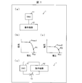
- FIG. 1 It is a figure which shows the structure of the photovoltaic device of Embodiment 1, Comprising: (a) is a block diagram which shows schematic structure of a photovoltaic device, (b) is the light reception energy of the dye-sensitized solar cell with which a photovoltaic device is provided. It is a graph which shows the relationship between the voltage and electric current which a dye-sensitized solar cell outputs when there is much, (c) is a graph which shows the said relationship when the said energy is small, (d) is a photovoltaic power generation It is a block diagram which shows a structure when an apparatus is provided with a variable resistance.
- FIG. 2 It is a figure which shows the structure of the photovoltaic device of Embodiment 2, Comprising: (a) is a block diagram which shows the structure by which the dye-sensitized solar cell was connected in parallel, (b) is a dye-sensitized solar cell in series. It is a block diagram which shows the structure connected to (c), (c) is a graph which shows the fluctuation
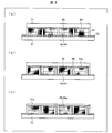
- FIG. 7 is a cross-sectional view showing an example of an integrated structure of each cell in the configuration in which the photovoltaic device shown in FIG. 6 is configured by a plurality of cells, where (a) shows a W-type integrated structure and (b) shows a Z-type integrated structure. A structure is shown, (c) shows a monolithic integrated structure.
- Embodiment 1 The first embodiment of the present invention will be described below with reference to FIGS.
- FIG. 1 is a diagram illustrating a configuration of a photovoltaic device 1 according to the present embodiment, where (a) is a block diagram illustrating a schematic configuration of the photovoltaic device 1, and (b) is a DSC 11 provided in the photovoltaic device 1. It is a graph which shows the relationship between the voltage and current which DSC11 outputs when there is much light reception energy of (c), (c) is a graph which shows the said relationship when the said energy is small, (d) is a photovoltaic device 1 is a block diagram showing a configuration when 1 includes a variable resistor 13. FIG.
- the photovoltaic device 1 includes a dye-sensitized solar cell (DSC) 11 (photovoltaic unit) and an operation device 12 (device). Yes.
- DSC dye-sensitized solar cell
- DSC 11 converts light into electric power.
- the operating device 12 is operated by the power generated by the DSC 11 through photoelectric conversion.
- an infrared sensor such as a human sensor
- a temperature sensor such as a temperature sensor
- an illuminance sensor such as a gas sensor
- a moving object sensor such as a Doppler radar sensor
- the operation device 12 uses a sensor with relatively small power consumption among general sensors.
- a device with relatively small power consumption is suitable as the operating device 12 of the present embodiment.
- Solar cells have the property that the current that can be taken out is determined by the voltage applied to the connected load.
- operating point refers to the operating state of the DSC 11 that is specified by the voltage and current output by the DSC 11 when the DSC 11 connected to the device (load) receives light and operates the device. Is a variable that represents
- the intensity and / or amount of light received by the DSC can vary due to various causes.
- the intensity and / or amount of received light varies, the energy per unit time of the light varies, so the power generated by the DSC also varies.
- the voltage and / or current output by the DSC 11 varies.
- the DSC 11 When the energy per unit time of light received by the DSC 11 (hereinafter simply referred to as the light receiving energy of the DSC 11) is relatively large, the DSC 11 has a relatively short circuit current as shown in FIG. The voltage-current characteristic that increases is shown.
- the operating point of the DSC 11 is set to the operating point P1.
- the DSC 11 When the light receiving energy of the DSC 11 is relatively small, the DSC 11 exhibits a voltage-current characteristic in which the short circuit current is relatively small as shown in FIG. In this case, the operating point of the DSC 11 is set to an operating point P2 that is hardly different from the operating point P1.
- the “optimal operating point” means an operating point specified by the voltage and current when the power output by the DSC 11 is maximized.
- the “non-operating point” means an operating point specified by an open circuit voltage when the output of the DSC 11 is open and a current having a value of 0. At the non-operating point, the power converted from light by the DSC 11 is zero.
- the operation points Pmax1 and Pmax2 shown in FIGS. 1B and 1C are optimum operation points (hereinafter, the operation point Pmax is referred to as the optimum operation point Pmax).
- the operating point Poc shown in FIGS. 1B and 1C is a non-operating point (hereinafter, the operating point Poc is referred to as a non-operating point Poc).
- the power consumption characteristic of the operating device 12 is such that the operating point of the DSC 11 is included in the range between the two excluding the optimal operating point Pmax1 and the non-operating point Poc. (Described later).
- the operating point of the DSC 11 is in the range between the two excluding the optimal operating point Pmax2 and the non-operating point Poc by the same setting of the power consumption characteristics of the operating device 12. It has been included.
- the deviation between the operating point P1 and the operating point P2 is smaller than the deviation of the optimal operating point even if the received light energy of the DSC 11 fluctuates only by appropriately determining the power consumption characteristics of the operating device 12. ing. This will be further described.
- FIG. 2A and 2B are graphs for comparing fluctuations in the operating point associated with fluctuations in the received energy of the DSC.
- FIG. 2A shows the fluctuation state of the optimum operating point of the conventional DSC
- FIG. 2B shows the light shown in FIG. The fluctuation state of the operating point of DSC of the power generator 1 is shown.
- the operating points P101 to P104 of the conventional DSC shown in FIG. 2 (a) are optimum operating points.
- MPPT maximum power tracking
- the operating point P1 of the DSC 11 shown in FIG. 2B is included in the range between the two except for the optimal operating point Pmax1 and the non-operating point Poc.
- the operating point P2 is included in a range between the two excluding the optimum operating point Pmax2 and the non-operating point Poc.
- the operating point P3 is included in a range between the two excluding the optimum operating point Pmax3 and the non-operating point Poc.
- the operating point P4 is included in a range between the two excluding the optimum operating point Pmax4 and the non-operating point Poc.
- the current values at the operating points P1 to P4 are substantially equal to each other.
- the deviation of the current at the operating points P1 to P4 is within ⁇ 5% of the average current value.
- the voltage values at the operating points P1 to P4 are also substantially equal to each other.
- the voltage deviation at the operating points P1 to P4 is within ⁇ 5% of the average voltage value.
- the current deviation ( ⁇ ⁇ I) and voltage deviation ( ⁇ ⁇ V) shown as the range ⁇ in FIG. 2B are the values of the current flowing through the operating device 12 or the voltage applied thereto. It must be within the fluctuation range (rated current range and / or rated voltage range) allowed for normal operation. As a result, since a current deviating from the rated current does not flow or a voltage deviating from the rated voltage is not applied to the operating device 12, stable operation of the operating device 12 is ensured and the operating device 12 is not affected. Can be prevented.
- the operating device 12 is directly or indirectly connected to the DSC 11 so as to consume power converted from light by the DSC 11. How much power is converted and consumed is determined by the power consumption characteristics of the operating device 12. If the power consumed by the operating device 12 is determined, the operating point of the DSC 11 specified by the voltage and current output by the DSC 11 is also determined.
- the power consumption characteristic of the operating device 12 may be the resistance of the operating device 12.
- the operating point is determined only by determining the resistance of the operating device 12 regardless of the type of the DSC 11.
- the resistance (value) of the operating device 12 is high, the voltage output by the DSC 11 increases and the current output by the DSC 11 decreases. As a result, the operating points P1 to P4 shown in FIG. 2B approach the non-operating point Poc. By increasing the resistance of the operating device 12, the deviation between the operating points P1 to P4 decreases as the operating points P1 to P4 approach the non-operating point Poc.
- the motion device 12 operates normally in the voltage range of 4.75V to 5.25V (that is, the rated voltage range is 5V (center voltage) ⁇ 5%) (for example, manufactured by Parallax) Was used.
- the operating voltage of the moving body sensor falls within a voltage range of 4.75V to 5.25V regardless of how the received energy of the DSC 11 varies. be able to. If the operating voltage falls within the rated voltage range, the operating current naturally falls within the rated current range.
- a moving body sensor that operates normally in a voltage range of 4.8V to 5.2V
- an infrared sensor that operates normally in a voltage range of 2.2V to 15V.
- those manufactured by Nippon Ceramics Co., Ltd. may be used.
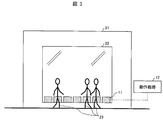
- FIG. 3 is a diagram illustrating an installation example of the photovoltaic power generation apparatus 1 illustrated in FIG. 1.
- the photovoltaic power generation apparatus 1 operates by placing the DSC 11 on an article 22 (window, show window, etc.) installed indoors in the building 21, for example. Thereby, DSC11 can receive and generate
- the photovoltaic power generation apparatus when used indoors or semi-indoors as shown in FIG. 3, the light incident on the DSC is weaker than when receiving sunlight outdoors. Since the originally weak light is blocked by a passerby or the like, the power output by the DSC varies greatly as compared with the case where the photovoltaic power generation apparatus is used outdoors.
- the DSC 11 has the voltage shown in FIG. Output current. If the number of passers-by 23 is large, the energy per unit time of the light received by the DSC 11 is relatively small, so the DSC 11 outputs the voltage and current shown in FIG.
- the action of the passerby 23 blocking the light incident on the DSC 11 is reproduced by creating a shadow (an area where no light is incident) in one third of the light receiving surface of the DSC 11 due to an obstacle. .
- a DSC panel (hereinafter referred to as a panel) having a light receiving surface of 30 cm ⁇ 30 cm and a conversion efficiency of 8.5% is used.
- the light received by the panel has an energy per unit time area of 100 W / m 2 .
- the resistance element As the operating device 12, a resistance element having a resistance value of 150 ⁇ is used.
- the resistance element is a simulated resistor that simulates the operating device 12.
- the panel and the resistive element are configured so that the resistive element consumes the power generated by the panel.
- the optimal operating point of the panel is specified by a voltage of 4.2V and a current of 0.175A.
- the non-operating point of the panel is specified by a voltage of 5.4 V (open voltage) and a current of 0 A.
- the short circuit current of the panel is 0.246A.
- the operating point specified by the voltage and current output by the panel shown in Table 1 is included between the optimum operating point and the non-operating point.
- the voltage value when there is an obstacle is 0.1 V smaller than the voltage value when there is no obstacle. That is, the voltage value fluctuates by about 1.9% based on the voltage value of 5.3 V when there is no obstacle.
- the current value when there is an obstacle is 0.001 A smaller than the current value when there is no obstacle. That is, the current value fluctuates by about 2.8% based on 0.036 A which is a current value when there is no obstacle.
- Table 2 below shows simulation results when the same operating device 12 is operated at the optimum operating point in the simulation whose results are shown in Table 1.
- the voltage value fluctuates by about 9.3% based on the voltage value of 4.3 V when there is no obstacle. Compared with the fluctuation, the fluctuation (1.9%) of the voltage value in the simulation whose result is shown in Table 1 is smaller.
- the photovoltaic device 1 can suppress fluctuations in the operating point of the DSC 11. Thereby, even if the photovoltaic device 1 is installed in a place where the received light energy of the DSC 11 fluctuates, the operating device 12 can be operated more stably than in the past. Moreover, since it can suppress that DSC11 outputs the electric power which remove
- an operating point control circuit for example, a booster circuit or a step-down circuit
- the photovoltaic device 1 can be realized with a simple configuration. .
- the photovoltaic device 1 which is low-cost can be provided.
- the photovoltaic device 1 may further include a variable resistor 13 that consumes the power converted by the DSC 11 from light.
- a variable resistor 13 that consumes the power converted by the DSC 11 from light.
- the DSC 11 may be provided as an independent power source that supplies power to the operation device 12.
- the operating device 12 since the operating device 12 can use only the power whose fluctuation is suppressed, the operating device 12 can be surely operated more stably than before, and the failure of the operating device 12 can be prevented.
- a photovoltaic method for operating the DSC 11 in a range between the two excluding the point is also included in the present embodiment. The effect mentioned above is acquired by the said photovoltaic method.
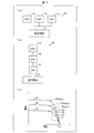
- FIG. 4 is a diagram illustrating the configuration of the photovoltaic power generation apparatuses 2a and 2A according to the present embodiment, in which (a) is a block diagram illustrating a configuration in which DSCs 11a, 11b, and 11c are connected in parallel, and (b) It is a block diagram which shows the structure by which DSC11A * 11B * 11C was connected in series, (c) is the fluctuation
- the photovoltaic device 2a includes DSCs 11a, 11b, and 11c (photovoltaic power generation unit) and an operation device 12 (device). Further, as shown in FIG. 4B, the photovoltaic device 2A includes DSCs 11A, 11B, and 11C (photovoltaic power generation unit) and an operation device 12 (device).
- the operating point Pa of the DSC 11a or 11A, the operating point Pb of the DSC 11b or 11B, and the operating point Pc of the DSC 11c or 11C are within the range ⁇ . include.
- the range ⁇ is obtained even when a current flows from one DSC among the DSCs 11a, 11b, and 11c to another DSC having a relatively low voltage when the received light energy of the DSCs 11a, 11b, and 11c greatly fluctuates. Even if the current flows from one DSC among the DSCs 11A, 11B, and 11C to another DSC having a relatively low voltage, the other DSC does not deteriorate the characteristics of the other DSC. The range in which the characteristics are not deteriorated. The range ⁇ is determined by experiments or the like.
- the curve aA shows the operation characteristic of DSC11a or 11A.
- the operating point Pmax_a indicates the optimum operating point of the DSC 11a or 11A.
- Curve bB shows the operating characteristics of DSC 11b or 11B.
- the operating point Pmax_b indicates the optimum operating point of the DSC 11b or 11B.
- a curve cC indicates the operating characteristics of the DSC 11c or 11C.
- the operating point Pmax_c indicates the optimum operating point of the DSC 11c or 11C.
- the operating point Poc indicates a non-operating point of the DSC 11a, 11b, 11c, 11A, 11B, or 11C.
- the operating point Pa is included in a range between the operating point Pmax_a and the operating point Poc.
- the operating point Pb is included in the range between the operating point Pmax_b and the operating point Poc.
- the operating point Pc is included in a range between the operating point Pmax_c and the operating point Poc.
- the difference between the voltage and current output by the DSCs 11a, 11b, 11c, 11A, 11B, and 11C causes shadows on the light receiving surfaces of the DSCs 11a, 11b, 11c, 11A, 11B, and 11C due to obstacles. Has been reproduced.
- a DSC panel (hereinafter, panel) a having a light receiving surface of 30 cm ⁇ 30 cm and having a conversion efficiency of 8.5% is used. Further, the panel b having the same configuration as the panel a is used as the DSCs 11b and 11B. Further, the panel c having the same configuration as the panel a is used as the DSCs 11c and 11C.
- the light received by the panels a, b, and c has energy per unit time area of 100 W / m 2 .
- the resistance element As the operating device 12, a resistance element having a resistance value of 150 ⁇ is used.
- the resistance element is a simulated resistor that simulates the operating device 12.
- the optimum operating point of panels a, b, and c is specified by a voltage of 4.2 V and a current of 0.175 A. Further, the non-operating points of the panels a, b, and c are specified by a voltage of 5.4 V (open voltage) and a current of 0 A.
- Table 3 shows the results of confirming the variation of the operating point when the panels a, b, and c are individually connected to the resistance elements.
- Table 3 is shown in the same format as Table 1.
- the voltage value when 50% of the light receiving surface of panel a is shaded by an obstacle is compared with the voltage value output by panel c when there is no obstacle. , 0.1V is smaller. That is, the voltage value fluctuates by about 1.9% based on the voltage value of 5.3 V when there is no obstacle.
- the current value when 50% of the light receiving surface of panel a is shaded by an obstacle is 0.001A smaller than the current value output by panel c when there is no obstacle. ing. That is, the current value fluctuates by about 2.8% based on 0.036 A which is a current value when there is no obstacle.
- the voltage value when a shadow is created in an area of 20% of the light receiving surface of the panel b by the obstacle is the same as the voltage value output by the panel c when there is no obstacle.
- the current value when a shadow is created in an area of 20% of the light receiving surface of the panel b due to the obstacle is the same as the current value output by the panel c when there is no obstacle.
- Table 4 shows the results of confirming the fluctuation of the operating point when the panels a, b, and c are connected in parallel as shown in FIG.
- Table 4 is shown in the same format as Table 1.
- the voltage value is Compared to the voltage value when there is no obstacle (corresponding to pattern 1), it is 0.05V smaller. That is, the voltage value fluctuates by about 0.9% based on the voltage value of 5.3 V when there is no obstacle.
- the current value is when there is no obstacle. Compared to the current value (corresponding to pattern 1), it is smaller by 0.002A. In other words, the current value fluctuates by about 1.9% based on 0.105 A, which is the current value when there is no obstacle.
- Table 5 shows the results of confirming the variation of the operating point when the panels a, b, and c are connected in parallel as shown in FIG.
- Table 5 is shown in the same format as Table 1.
- the voltage value is Compared to the voltage value when there is no obstacle (corresponding to pattern 1), it is 0.3V smaller. That is, the voltage value fluctuates by about 1.9% with reference to 16.0 V, which is the voltage value when there is no obstacle.
- the current value is when there is no obstacle. Compared to the current value (corresponding to pattern 1), it is 0.001A smaller. That is, the current value fluctuates by about 2.9% based on 0.035 A which is a current value when there is no obstacle.
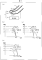
- FIGS. 5A and 5B are diagrams relating to the photovoltaic device 3 of the present embodiment, in which FIG. 5A is a diagram illustrating another installation example of the photovoltaic device 3, and FIG. It is a graph which shows the correlation of an operation characteristic, (c) is a graph which shows the other correlation of each said operation characteristic, (d) is a graph which shows the said correlation as a comparative example.
- the photovoltaic device 3 includes a DSC 11x / 11y (photovoltaic unit) and an operation device 12 (device).
- the motion device 12 is, for example, a human sensor that consumes power converted from light by the DSCs 11x and 11y, detects a user of the escalator 31, and transmits an operation start / stop signal to the escalator 31. Good.
- the DSC 11x / 11y / escalator 31 is connected in the same manner as the DSC 11a / 11b / operating device 12 shown in FIG. 4A (at this time, the DSC 11c does not exist).
- the DSC 11x / 11y / escalator 31 is connected in the same manner as the DSC 11A / 11B / operating device 12 shown in FIG. 4B (Note that the DSC 11C does not exist and the DSC 11B and the operating device 12 are connected.
- the DSC 11C does not exist and the DSC 11B and the operating device 12 are connected.
- the photovoltaic device 3 operates by placing DSCs 11x and 11y on the side walls 32x and 32y of the escalator 31, respectively.
- the DSCs 11x and 11y can generate power by receiving sunlight and / or light having a lighting device disposed in the vicinity of the place where the escalator 31 is installed as a light source.
- the number of users who use the escalator 31 per unit time varies. Furthermore, the light reception energy of the side wall 32x is different from the light reception energy of the side wall 32y. Below, the case where the light reception energy of the side wall 32y is smaller than the light reception energy of the side wall 32x is demonstrated.
- the operating point of the DSC 11x is on the curve indicated by the curve xa when the number of users per unit time using the escalator 31 is the smallest. Further, the operating point of the DSC 11x exists on the curve indicated by the curve xb when the number of persons is the largest. In addition, the operating point of the DSC 11y exists on the curve indicated by the curve ya when the number of persons is the smallest. In addition, the operating point of the DSC 11y exists on the curve indicated by the curve yb when the number of persons is the largest.
- the curve where the operating point of the DSC 11x exists is in the region between the curve xa and the curve xb. Further, the curve where the operating point of the DSC 11y exists is in a region between the curve ya and the curve yb.
- each region is referred to as a “variable region”.
- the operating point Pmax_xa represents an optimal operating point when the DSC 11x operates along the curve xa.
- the operating point Pmax_xb represents an optimal operating point when the DSC 11x operates along the curve xb.
- the operating point Pmax_ya represents an optimal operating point when the DSC 11y operates along the curve ya.
- the operating point Pmax_yb represents an optimal operating point when the DSC 11y operates along the curve yb.
- the operating point Poc represents a non-operating point of the DSC 11x and a non-operating point of the DSC 11y.
- Region D is a region between a range excluding operating point Pmax_xa and operating point Poc, a range between operating point Pmax_xb and operating point Poc, and operating point Pmax_ya and operating point Poc.
- a variable region that is a region between the range excluding the operating point Pmax_yb and the operating point Poc in the curve yb represents an overlapping region.
- the region D includes at least one overlapping point belonging to both the DSC 11x variable region and the DSC 11y variable region.
- the operating point of the DSC 11x can be set to an operating point included in the region D or an operating point near the region D by appropriately setting the resistance of the operating device 12.
- the operating point can be set to an operating point included in the region D or an operating point near the region D.
- each operation characteristic may be set so that the operation characteristic of the DSC 11x and the operation characteristic of the DSC 11y intersect each other.
- the operating point Poc_x represents a non-operating point of the DSC 11x.
- the operating point Poc_y represents a non-operating point of the DSC 11y.
- the region Da is a region between the range excluding the operating point Pmax_xa and the operating point Poc_x and the range between the operating point Pmax_xb and the operating point Poc_x, and the operating point Pmax_ya and the operating point Poc_y.
- a variable region that is a region between the range excluding the operating point Pmax_yb and the operating point Poc_y on the curve yb represents an overlapping region.
- the area Da includes at least one overlapping point belonging to both the fluctuation area of the DSC 11x and the fluctuation area of the DSC 11y.
- the operating point of the DSC 11x can be set to an operating point included in the area Da or an operating point near the area Da by appropriately setting the resistance of the operating device 12.
- the operating point can be set to an operating point included in the area Da or an operating point near the area Da.
- the DSCs 11x and 11y can be installed under different light irradiation conditions, it is possible to secure a larger installation area than before.
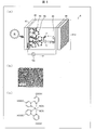
- FIG. 6 is a diagram illustrating the configuration of the photovoltaic device 4 of the present embodiment, in which (a) is a schematic diagram illustrating the overall configuration of the photovoltaic device 4, and (b) configures the solar battery cell 11d. It is an image which shows the titanium oxide microparticles
- the photovoltaic device 4 includes a solar battery cell 11d (photovoltaic power generation unit) and an external circuit 12d (device).
- the solar battery cell 11d includes a glass (hereinafter also referred to as “substrate”) 41, a transparent conductive film (hereinafter also referred to as “TCO”) 42, porous titanium oxide (hereinafter referred to as “porous titanium oxide film”, “ 43 ”, a dye 44, an electrolyte 45, and a counter electrode (hereinafter also referred to as“ counter electrode ”) 46.
- substrate glass
- TCO transparent conductive film
- porous titanium oxide film hereinafter referred to as “porous titanium oxide film”, “ 43 ”
- dye 44 an electrolyte 45
- counter electrode hereinafter also referred to as“ counter electrode ”
- a porous titanium oxide 43 is formed on a glass 41 substrate on which the TCO 42 is formed.
- the porous titanium oxide film 43 includes fine titanium oxide particles having a diameter of 10 to 20 nm shown in FIG.
- the dye 44 is, for example, a ruthenium (Ru) metal complex dye specified by the structural formula shown in FIG.
- the dye 44 is adsorbed on the surface of the porous titanium oxide film 43.
- the dye 44 has a functional group such as a carboxyl group, and the titanium oxide 43 and the dye 44 are chemically bonded by dehydrating the carboxyl group and titanium oxide.
- a catalyst that activates the oxidation-reduction reaction of the electrolyte 45 is formed on the counter electrode 46.
- An electrolyte 45 is infiltrated between the electrode having a structure including the transparent conductive film 42, the porous titanium oxide film 43, and the dye 44 and the counter electrode 46.
- FIG. 7 is a diagram showing a manufacturing procedure of the solar battery cell 11d included in the photovoltaic device 4 shown in FIG. 6, wherein (a) shows a step of preparing a glass substrate with a transparent conductive film, and (b) shows The process of producing a titanium oxide electrode is shown, (c) shows the glass substrate with a transparent conductive film on which the titanium oxide electrode was produced, (d) shows the process of adsorbing the dye, and (e) shows the solar cell. The process of assembling 11d is shown, (f) shows the assembled solar battery cell 11d.
- a paste in which titanium oxide fine particles are dispersed is applied onto a glass substrate with TCO and fired, so that it is porous.
- a titanium oxide film 43 is produced.
- the produced porous titanium oxide film 43 is immersed in the dye solution, thereby adsorbing the dye 44 on the titanium oxide surface.
- an electrolyte layer is formed between the glass with a transparent conductive film in which the pigment 44 is adsorbed on the titanium oxide surface and the counter electrode 46, and the periphery is sealed.
- the process cost can be greatly reduced as compared with the conventional photovoltaic power generation apparatus.
- the amount of the dye 44 to be adsorbed is increased to 800 to 1000 times by making the titanium oxide that adsorbs the dye 44 porous and increasing the specific surface area.
- Highest Occupied Molecular Orbital) -LUMO (Lowest Unoccupied Molecular Orbital) level can be controlled to energy distribution and spatial distribution suitable for the titanium oxide 43 to be adsorbed.
- the following configurations (1) to (2) are listed as configurations for changing the power generation efficiency.
- the photovoltaic device 4 introduces an alternating current impedance method into the resistance analysis of the photovoltaic device 4, conducts resistance analysis at each interface, and the internal structure of the photovoltaic device 4. Or feedback on material development. Thereby, the internal resistance of the photovoltaic device 4 can be reduced.
- the light receiving area of the photovoltaic device 4 is increased.
- a plurality of solar cells 11d hereinafter referred to as “cells”
- the cells are thin film solar cells such as thin film silicon solar cells and dye-sensitized solar cells
- a plurality of cells may be integrated on a glass substrate 51 as a light receiving surface of the photovoltaic device 4.
- FIG. 8 is a cross-sectional view showing an example of the integrated structure of each cell in the configuration in which the photovoltaic power generation device 4 shown in FIG. 6 is configured by a plurality of cells, where (a) shows a W-type integrated structure, ) Shows a Z-type integrated structure, and (c) shows a monolithic integrated structure.
- a substrate (hereinafter also referred to as “substrate with TCO”) 51 (a glass 41 is processed) on which a conductive layer 54 is formed at a predetermined location. Every other element including the electrolyte 45, the titanium oxide 43, and the dye 44 is formed on the substrate 51 and the substrate 51 on which the TCO 52 (processed TCO 42) is formed at a predetermined location.
- the photovoltaic device 4 may include a W-type integrated structure in which the substrates are bonded so that the elements formed on the two substrates are staggered. Thereby, each cell is connected in series. In the W-type integrated structure, the photovoltaic device 4 may further include a sealing layer 53 and a conductive layer 54.
- the W-type integrated structure cells can be connected in series simply by bonding two substrates 51 with TCO, so that a high-density integrated structure can be easily formed. Further, by providing the W-type integrated structure and the above-described “configuration for changing power generation efficiency”, when the photovoltaic power generation device 4 is an integrated dye-sensitized solar cell having a size of 5 cm square, 8.4% energy is obtained. Conversion efficiency can be achieved.
- the photovoltaic device 4 For example, as shown in FIG. 8B, in the photovoltaic device 4, an element is produced on one substrate 51 with TCO, and the other substrate 51 with TCO is used as a counter electrode. It's okay. Then, the photovoltaic device 4 has a Z-type integrated structure in which the connection layer 55 for electrically connecting the cell and the counter electrode adjacent to each other is manufactured by bonding the substrate 51 with the TCO on which the element is manufactured and the counter electrode. May be provided. Thereby, each element is connected in series.
- the photovoltaic device 4 has a structure in which the substrate 51 with TCO in the Z-type integrated structure shown in FIG.
- a monolithic integrated structure may be provided in which each layer such as titanium 43 is sequentially formed directly on the lower layer and finally the cells are connected in series.
- the photovoltaic device 4 may further include a cover material 51a and a porous insulating layer 45a.
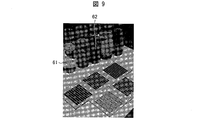
- FIG. 9 is an image showing the color variation of the dye 44 of the photovoltaic device 4 shown in FIG.
- the pigment 44 of the photovoltaic device 4 has various color variations.
- the solar battery cell 11 d of the photovoltaic power generation device 4 may include different color pigments 44.
- the pigment 44 may include a green pigment 61 and a red brown pigment 62.
- the dye 44 may include a dye having an absorption peak with respect to light received by the solar battery cell 11d in a specific wavelength range.
- a plurality of types of dyes 44 may be adsorbed on the surface of the porous titanium oxide film 43 (coadsorption).
- the red-brown dye 62 (for example, a dye having an absorption peak at a wavelength of about 550 nm) is compared with the green-colored dye 61 (for example, a dye having an absorption peak at a wavelength of about 630 nm).
- the gap between orbital (Highest Occupied Molecular Orbital) -LUMO (lowest empty orbit; LowestLowUnoccupied Molecular Orbital) tends to increase the voltage output by the photovoltaic unit.
- the green pigment 61 has an absorption peak on the long wavelength side as compared with the red-brown 62 pigment, and the wavelength range of the light to be absorbed is widened, so that the current output from the photovoltaic unit tends to increase.
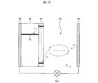
- FIG. 10 is a conceptual diagram showing the operation of the photovoltaic power generation apparatus 4 shown in FIG.
- the dye 44 absorbs light and excites electrons e.
- the electrons e are injected into the conduction band 72 of the porous titanium oxide 43 in a time order of 10 ⁇ 12 seconds, and are carried to the external circuit 12d via the TCO 42.
- Oxidized dye 44 receives electrons e from electrolyte 45 labeled I ⁇ and returns to the ground state (the state before being oxidized).
- the electrolyte 45 indicated as I 3 ⁇ oxidized by the dye 44 diffuses to the counter electrode 46, receives the electron e from the counter electrode 46, and returns to the electrolyte 45 in the reduced state indicated as I ⁇ .
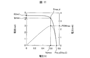
- FIG. 11 is a graph showing the current output by the photovoltaic power generation apparatus 4 and the power generated by the photovoltaic power generation apparatus 4 with respect to the voltage output by the photovoltaic power generation apparatus 4 shown in FIG.
- the horizontal axis indicates the value of the voltage output from the photovoltaic device 4.
- the left vertical axis represents the value of the current output from the photovoltaic device 4.
- the vertical axis on the right indicates the value of power generated by the photovoltaic device 4.
- the upper solid line represents the relationship between voltage and current.
- the lower solid line represents the relationship between voltage and power.
- the voltage Vpmax corresponding to the operating point Pmax_d (the operating point when the power POWmax is 2.429 mW), which is the optimum operating point, is 0.583 V, and the current Ipmax is 4.16 mA. is there.
- the voltage Voc which is an open circuit voltage is 0.736V.
- the current Isc which is a short-circuit current, is 4.57 mA.
- the operating point of the solar battery cell 11d is included between the operating point Pmax_d and the operating point Poc_d.
- the solar battery cell 11d includes the pigment 44 having a different color, so that the spectral spectrum of the sunlight changes depending on the time or the type of the light source that is turned on indoors changes. Even if it does, it can suppress that power generation amount falls.
- the photovoltaic device 4 excellent in design property in which the solar battery cell 11d is colored in various colors can be provided.
- the solar battery cell 11d when the solar battery cell 11d includes the dye 44 having an absorption peak for light in a specific wavelength region, light in a specific wavelength region is selectively selected from light received by the solar battery cell 11d. Can be converted into electric power. For example, light in a specific wavelength range is selectively converted into electric power, whereby the amount of electric power conversion can be changed and the operating point of the solar battery cell 11d can be controlled.
- the solar battery cell 11d With respect to light received by the solar battery cell 11d (for example, light using asahi, daytime sunlight, sunset, fluorescent light as a light source, or light emitting diode (LED) as a light source), By using a dye having an absorption peak in the wavelength range where the light intensity is strongest, the power generation efficiency of the solar battery cell 11d can be maximized.
- light received by the solar battery cell 11d for example, light using asahi, daytime sunlight, sunset, fluorescent light as a light source, or light emitting diode (LED) as a light source
- LED light emitting diode
- the photovoltaic devices 1, 2a, 2A, 3 and 4 include photovoltaic units (dye-sensitized solar cells 11, 11a to 11c, 11A to 11C, 11x and 11y, which convert light into electric power).
- Solar cell 11d and devices (operating device 12, external circuit 12d) that operate with the power, the devices operating points Pmax1 to Pmax4 ⁇ Pmax_a of the photovoltaic unit when the power reaches a maximum.
- the operating point of the photovoltaic unit when the light received by the photovoltaic unit varies, the operating point of the photovoltaic unit also varies. Conventionally, the operating point is controlled so that the fluctuation is not taken into consideration and the power converted by the photovoltaic power generation unit is simply maximized.
- the operating point is included in the range between the operating point when the power is maximized and the non-operating point except for the operating point.
- a control circuit for adjusting the output voltage of the photovoltaic power generation unit is not required, and it is only necessary to set the power consumption characteristics of the device.
- the fluctuation range of the voltage output from the photovoltaic unit may be a center voltage ⁇ 5%.
- the power consumption characteristic may be a resistance of the device.
- the photovoltaic unit it is possible to cause the photovoltaic unit to perform an operation with reduced fluctuations in the operating point, simply by determining the resistance of the device, regardless of the type of the photovoltaic unit.
- the photovoltaic device according to the fourth aspect of the present invention may further include the variable resistor 13 that consumes the power in any one of the first to third aspects.
- the optimum operating point can be easily set by the variable resistor.
- the photovoltaic device according to the fifth aspect of the present invention is the photovoltaic device according to any one of the first to fourth aspects, even if a current flows from one photovoltaic unit to the other photovoltaic unit having a relatively low voltage, You may provide the said several photovoltaic power generation part which does not degrade the characteristic of the said other photovoltaic power generation part.
- a photovoltaic device is the photovoltaic device according to any one of Aspects 1 to 5, in which the operating point of one of the photovoltaic power generation units is included, and the other photovoltaic power generation unit.
- the range between the two points including the operating point may include a plurality of the photovoltaic units having overlapping points (regions D and Da).
- the overlapping point or the overlapping point can be operated at an operating point close to. In other words, even when a plurality of photovoltaic units are placed under different light irradiation conditions, fluctuations in the operating points of the plurality of photovoltaic units can be suppressed.
- the photovoltaic power generation apparatus may be controlled by a photovoltaic power generation control apparatus realized by a computer described later.
- the photovoltaic power generation unit may be provided as an independent power source that supplies power to the device.
- the device can use only the electric power whose fluctuation is suppressed, the device can be surely operated more stably than before, and the failure of the device can be prevented.
- the power generated by the photoelectric conversion of the photovoltaic power generation units (the dye-sensitized solar cells 11 ⁇ 11a to 11c ⁇ 11A to 11C ⁇ 11x ⁇ 11y, the solar cells 11d) is supplied.
- the operating points Pmax1 to Pmax4 ⁇ Pmax_a to Pmax_d ⁇ Pmax_xa ⁇ Pmax_xb ⁇ Pmax_ya ⁇
- the photovoltaic unit is operated in a range between Pmax_yb ⁇ Pmax_x to Pmax_y and a non-operating point (operating point Poc ⁇ Poc_x to Poc_y) when the photovoltaic unit is open.
- the photovoltaic power generation apparatus may be controlled by a photovoltaic power generation control apparatus realized by a computer.
- the photovoltaic power generation control device is a photovoltaic power generation control device that controls a photovoltaic power generation device including a photovoltaic power generation unit that converts light into electric power, and a device connected to the photovoltaic power generation unit, Operating point information acquisition means for acquiring information representing the operating point of the photovoltaic unit when power is maximized, and a non-operating point for acquiring information representing a non-operating point when the photovoltaic unit is open Using the information acquired by the information acquisition means, the operating point information acquisition means and the non-operating point information acquisition means, the device operates at the operating point of the photovoltaic unit when the power is maximized, and For setting the operating point of the photovoltaic unit to have power consumption characteristics for operating the photovoltaic unit in a range between the two except for the non-operating point when the photovoltaic unit is open Operating point setting information generating means for generating information
- the operating point information acquiring unit and the non-operating point information acquiring unit dynamically acquire information, so that the operating point setting information generating unit can stabilize the operation of the device and cause a failure as described above.
- Information for setting an operating point that can be prevented can be dynamically generated. Therefore, if the information is used, the operation of the device can be stabilized and the failure can be prevented regardless of the type and / or state of the photovoltaic unit and / or the device. Furthermore, by causing the computer to function as each means, it is possible to automate the operation stabilization and failure prevention of the device.
- a program for a photovoltaic power generation control device that causes the photovoltaic power generation control device to be realized by a computer by operating the computer as each unit included in the photovoltaic power generation control device, and a computer-readable recording medium that records the program are also provided. It falls into the category of the invention.
- the present invention is used for, for example, a photovoltaic device for generating electric power consumed by devices such as an infrared sensor (such as a human sensor), a temperature sensor, an illuminance sensor, a gas sensor, and a moving object sensor (such as a Doppler radar sensor).
- devices such as an infrared sensor (such as a human sensor), a temperature sensor, an illuminance sensor, a gas sensor, and a moving object sensor (such as a Doppler radar sensor).
Landscapes
- Engineering & Computer Science (AREA)
- Power Engineering (AREA)
- Chemical & Material Sciences (AREA)
- Chemical Kinetics & Catalysis (AREA)
- Electrochemistry (AREA)
- Microelectronics & Electronic Packaging (AREA)
- Photovoltaic Devices (AREA)
- Direct Current Feeding And Distribution (AREA)
- Control Of Electrical Variables (AREA)
Abstract
Description
本発明の第一実施形態について、図1~図3に基づいて説明すれば、以下のとおりである。
図1は、本実施形態の光発電装置1の構成を示す図であって、(a)は光発電装置1の概略構成を示すブロック図であり、(b)は光発電装置1が備えるDSC11の受光エネルギーが多いときの、DSC11が出力する電圧と電流との関係を示すグラフであり、(c)は当該エネルギーが少ないときの、当該関係を示すグラフであり、(d)は光発電装置1が可変抵抗13を備えるときの構成を示すブロック図である。
太陽電池は、接続した負荷にかかる電圧によって、取り出せる電流が決まるという性質がある。以下において「動作点」とは、機器(負荷)に接続されたDSC11が光を受光して機器を動作させているときに、DSC11が出力する電圧と電流とにより特定される、DSC11の動作状態を表す変数である。
動作機器12は、DSC11によって光から変換された電力を消費するように、直接にまたは間接的にDSC11と接続される。電力がどの程度変換され消費されるかは、動作機器12が有する電力消費特性によって定まる。動作機器12が消費する電力が定まれば、DSC11によって出力される電圧と電流とにより特定されるDSC11の動作点も定まる。
動作機器12として、4.75V以上5.25V以下の電圧範囲で正常に動作する(つまり、定格電圧範囲が5V(中心電圧)±5%である)動体センサー(例えば、Parallax社製のもの)を用いた。この場合、適切な抵抗値を備えた動体センサーを選択することによって、DSC11の受光エネルギーがどのように変動しても、動体センサーの動作電圧を4.75V以上5.25V以下の電圧範囲に収めることができる。動作電圧が定格電圧範囲に収まれば、動作電流も自ずと、定格電流範囲に収まる。
図3は、図1に示される光発電装置1の設置例を示す図である。
図3に示される状況を再現するシミュレーションを実施した。
以下の表1は、図3に示される状況を再現したシミュレーション結果を示す。

以下の表2は、表1に結果が示されるシミュレーションにおいて、同じ動作機器12に対して最適動作点で動作するようにしたときのシミュレーション結果を示す。

以上のように、光発電装置1は、DSC11の動作点の変動を抑制できる。これにより、DSC11の受光エネルギーが変動する場所に、光発電装置1を設置したとしても、動作機器12を従来よりも安定して動作させることができる。また、DSC11が、動作機器12が正常に動作できる範囲から外れる電力を出力することを抑制できるので、動作機器12を従来よりも安定して動作させるとともに、動作機器12の故障を防止することもできる。
図1の(d)に示されるように、光発電装置1は、DSC11が光から変換した電力を消費する可変抵抗13をさらに備えてよい。この場合、可変抵抗13によって、光発電装置1全体の抵抗を調整できるので、最適な動作点の設定が容易になる。
本発明の第二実施形態について、図4に基づいて説明すれば、以下のとおりである。なお、説明の便宜上、上述の実施形態にて説明した部材と同じ機能を有する部材については、同じ符号を付記し、その説明を省略する。
図4は、本実施形態の光発電装置2a・2Aの構成を示す図であって、(a)はDSC11a・11b・11cが並列に接続された構成を示すブロック図であり、(b)はDSC11A・11B・11Cが直列に接続された構成を示すブロック図であり、(c)は(a)に示される光発電装置2aと(b)に示される光発電装置2Aとにおける動作点の変動状態を示すグラフである。
光発電装置2a・2Aでは、図4の(c)に示されるように、DSC11aまたは11Aの動作点Paと、DSC11bまたは11Bの動作点Pbと、DSC11cまたは11Cの動作点Pcとは、範囲βに含まれる。
図4の(a)・(b)・(c)に示される状況を再現するための複数のシミュレーションを実施した。
以下の表3は、パネルa・b・cが個別に抵抗素子へ接続された場合の、動作点の変動を確認した結果を示す。

以下の表4は、パネルa・b・cが、図4の(a)に示されるように、並列に接続された場合の、動作点の変動を確認した結果を示す。

以下の表5は、パネルa・b・cが、図4の(b)に示されるように、並列に接続された場合の、動作点の変動を確認した結果を示す。

従来では、複数のDSCが接続された形態で各DSCの受光エネルギーが変動した場合、各DSCが出力する電圧と電流との相違に起因し、電圧が相対的に高いDSCから電圧が相対的に低いDSCへ、電流が流れこむことがあった。
以上のように、DSC11a・11b・11cの間における電流の流れこみによるDSC11a・11b・11c・11A・11B・11Cの故障を防止できる。また、DSC11A・11B・11Cの間における電流の流れこみによるDSC11A・11B・11Cの故障を防止できる。また、電流が律速されることを防止できる。
本発明の第三実施形態について、図5に基づいて説明すれば、以下のとおりである。なお、説明の便宜上、上述の実施形態にて説明した部材と同じ機能を有する部材については、同じ符号を付記し、その説明を省略する。
図5は、本実施形態の光発電装置3に関する図であって、(a)は光発電装置3の他の設置例を示す図であり、(b)はDSC11x・11yを接続する形態における各動作特性の相互関係を示すグラフであり、(c)は上記各動作特性の他の相互関係を示すグラフであり、(d)は比較例としての当該相互関係を示すグラフである。
図5の(b)に示されるように、DSC11xの動作点は、エスカレータ31を利用する利用者の単位時間あたりの人数が最も少ないときには、曲線xaによって示される曲線上に存在する。また、DSC11xの動作点は、当該人数が最も多いときには、曲線xbによって示される曲線上に存在する。また、DSC11yの動作点は、当該人数が最も少ないときには、曲線yaによって示される曲線上に存在する。また、DSC11yの動作点は、当該人数が最も多いときには、曲線ybによって示される曲線上に存在する。
図5の(c)に示されるように、DSC11xの動作特性と、DSC11yの動作特性とが、交差するように、各動作特性を設定してもよい。
以上により、DSC11xと、DSC11yとによって受光される光における単位時間あたりのエネルギーが互いに異なっても、DSC11xの変動領域と、DSC11yの変動領域とが重複する領域(領域D・Da)を有することにより、当該重複する領域に含まれる領域、または、当該重複する領域に近い領域において、DSC11x・11yを動作させることができる。これにより、DSC11xの動作特性と、DSC11yの動作特性とを近づけることができるので、一方のDSCから他方のDSCへ電流が流れ込み、DSCの特性を低下させる問題や、動作機器12に印加される電圧が変動する問題を抑制することができる。
光発電装置のDSCが、上述の領域D・Daを有さない場合、図5の(d)において、矢印Eで示されるように、曲線xa・xbと、曲線ya・ybとが乖離する。このように動作特性が乖離している場合には、一方のDSCから他方のDSCへ電流が流れ込み、DSCの特性を低下させる問題や、動作機器12に印加される電圧が変動する問題を抑制することができない。
本発明の第四実施形態について、図6~11に基づいて説明すれば、以下のとおりである。なお、説明の便宜上、上述の実施形態にて説明した部材と同じ機能を有する部材については、同じ符号を付記し、その説明を省略する。
(基本構成)
図6は、本実施形態の光発電装置4の構成を示す図であって、(a)は光発電装置4の全体構成を示す模式図であり、(b)は太陽電池セル11dを構成する多孔質酸化チタンが含む酸化チタン微粒子を示す画像であり、(c)は太陽電池セル11dに用いる色素44の分子構造を示す構造式である。
図7は、図6に示される光発電装置4が備える太陽電池セル11dの製作手順を示す図であって、(a)は透明導電膜付きガラス基板を準備する工程を示し、(b)は酸化チタン電極を作製する工程を示し、(c)は酸化チタン電極が作製された透明導電膜付きガラス基板を示し、(d)は、色素を吸着させる工程を示し、(e)は太陽電池セル11dを組み立てる工程を示し、(f)は組み立てられた太陽電池セル11dを示す。
光発電装置4では、色素44を吸着させる酸化チタンを多孔質にし、比表面積を広げることにより、吸着させる色素44の量を800~1000倍までに引き上げるとともに、色素44のHOMO(最高被占軌道;Highest Occupied Molecular Orbital)-LUMO(最低空軌道;Lowest Unoccupied Molecular Orbital)準位を、吸着させる酸化チタン43に適したエネルギー分布と空間分布とに制御できる。
そして、光発電装置4では、上記(1)を実現するために、光発電装置4内部の光閉じ込め効果の指標としてのヘイズ率を考慮した、酸化チタン微粒子の粒径制御などにより、多孔質酸化チタン43内部の光閉じ込めを実施してよい。これにより、光発電装置4が出力する電流を高めることができる。
光発電装置4が出力する電圧・電流を大きくする場合、例えば、光発電装置4の受光面積を大きくする。ここで、複数の太陽電池セル11d(以下、「セル」と記載)を並列または直列に接続し、かつ、セルを薄膜シリコン太陽電池や色素増感太陽電池などの薄膜型太陽電池とすれば、光発電装置4の受光面とするガラスの基板51上に、複数のセルを集積してよい。
図9は、図6に示される光発電装置4の色素44のカラーバリエーションを示す画像である。
異なる色の色素44は、光の吸収ピーク波長が異なるので、異なる色の色素44を利用すれば、発電に使える光の波長範囲を広げることができる。
以上のように、太陽電池セル11dは、異なる色の色素44を含むことにより、太陽光の分光スペクトルが時刻によって変化したり、屋内で点灯される光源の種類が変わることによって、分光スペクトルが変化したりしても、発電量が低下することを抑止できる。
本発明の態様1に係る光発電装置1・2a・2A・3・4は、光を電力に変換する光発電部(色素増感太陽電池11・11a~11c・11A~11C・11x・11y、太陽電池セル11d)と、上記電力によって動作する機器(動作機器12、外部回路12d)とを備え、上記機器は、上記電力が最大となるときの上記光発電部の動作点Pmax1~Pmax4・Pmax_a~Pmax_d・Pmax_xa・Pmax_xb・Pmax_ya・Pmax_yb・Pmax_x~Pmax_yと、上記光発電部が開放されているときの上記光発電部の非動作点(動作点Poc・Poc_x~Poc_y)とを除く両者の間の範囲で、上記光発電部を動作させる電力消費特性を有している。
本発明の各態様に係る光発電装置は、コンピュータによって実現された光発電制御装置によって制御されてもよい。
本発明は上述した各実施形態に限定されるものではなく、請求項に示した範囲で種々の変更が可能であり、異なる実施形態にそれぞれ開示された技術的手段を適宜組み合わせて得られる実施形態についても本発明の技術的範囲に含まれる。さらに、各実施形態にそれぞれ開示された技術的手段を組み合わせることにより、新しい技術的特徴を形成することができる。
11・11a~11c・11A~11C・11x・11y 色素増感太陽電池(光発電部)
11d 太陽電池セル(光発電部)
12 動作機器(機器)
12d 外部回路(機器)
13 可変抵抗
44 色素
61 緑系色素
62 赤茶系色素
D・Da 領域(重複点)
P1~P4・Pa~Pc 動作点
Pmax1~Pmax4・Pmax_a~Pmax_d・Pmax_xa・Pmax_xb・Pmax_ya・Pmax_yb・Pmax_x~Pmax_y 動作点
Poc・Poc_x~Poc_y 動作点(非動作点)
Claims (5)
- 光を電力に変換する光発電部と、
上記電力によって動作する機器とを備え、
上記機器は、上記電力が最大となるときの上記光発電部の動作点と、上記光発電部が開放されているときの上記光発電部の非動作点とを除く両者の間の範囲で、上記光発電部を動作させる電力消費特性を有していることを特徴とする光発電装置。 - 上記光発電部が出力する電圧の変動範囲は、中心電圧±5%であることを特徴とする請求項1に記載の光発電装置。
- 上記電力消費特性は、上記機器が有している抵抗であることを特徴とする請求項1または2に記載の光発電装置。
- 一つの上記光発電部の動作点が含まれる上記両者の間の範囲と、他の上記光発電部の動作点が含まれる上記両者の間の範囲とは、重複点を有する、複数の上記光発電部を備えることを特徴とする請求項1から3のいずれか1項に記載の光発電装置。
- 上記光発電部は、上記機器に電力を供給する独立電源として設けられていることを特徴とする請求項1から4のいずれか1項に記載の光発電装置。
Priority Applications (3)
| Application Number | Priority Date | Filing Date | Title |
|---|---|---|---|
| JP2016519166A JP6472791B2 (ja) | 2014-05-12 | 2015-04-14 | 光発電装置 |
| EP15793331.8A EP3144945B1 (en) | 2014-05-12 | 2015-04-14 | Light power generation apparatus |
| US15/310,579 US20170085089A1 (en) | 2014-05-12 | 2015-04-14 | Photovoltaic power generation apparatus |
Applications Claiming Priority (2)
| Application Number | Priority Date | Filing Date | Title |
|---|---|---|---|
| JP2014-099034 | 2014-05-12 | ||
| JP2014099034 | 2014-05-12 |
Publications (1)
| Publication Number | Publication Date |
|---|---|
| WO2015174188A1 true WO2015174188A1 (ja) | 2015-11-19 |
Family
ID=54479732
Family Applications (1)
| Application Number | Title | Priority Date | Filing Date |
|---|---|---|---|
| PCT/JP2015/061449 Ceased WO2015174188A1 (ja) | 2014-05-12 | 2015-04-14 | 光発電装置 |
Country Status (4)
| Country | Link |
|---|---|
| US (1) | US20170085089A1 (ja) |
| EP (1) | EP3144945B1 (ja) |
| JP (1) | JP6472791B2 (ja) |
| WO (1) | WO2015174188A1 (ja) |
Citations (5)
| Publication number | Priority date | Publication date | Assignee | Title |
|---|---|---|---|---|
| JPS53112380U (ja) * | 1977-02-14 | 1978-09-07 | ||
| JPS6268256U (ja) * | 1985-10-19 | 1987-04-28 | ||
| JP2001141851A (ja) * | 1999-11-18 | 2001-05-25 | Minolta Co Ltd | 透光性太陽電池付き電子機器 |
| JP2011078215A (ja) * | 2009-09-30 | 2011-04-14 | Panasonic Electric Works Co Ltd | 配電システム |
| JP2012078090A (ja) * | 2010-09-30 | 2012-04-19 | Mitsumi Electric Co Ltd | 電流電圧検出回路および電流制御回路 |
Family Cites Families (7)
| Publication number | Priority date | Publication date | Assignee | Title |
|---|---|---|---|---|
| DE3729000A1 (de) * | 1987-08-31 | 1989-03-09 | Rudolf Kiesslinger | Universalregler zur leistungsmaximierung photovoltaischer stromversorgungen und fuer hocheffiziente gleichspannungswandler |
| US4982176A (en) * | 1990-01-17 | 1991-01-01 | Frank Schwarz | Solar powered lighting and alarm systems activated by motion detection |
| JP2003333757A (ja) * | 2002-05-14 | 2003-11-21 | Sony Corp | 電源装置 |
| US20100116325A1 (en) * | 2008-11-12 | 2010-05-13 | Mehrdad Nikoonahad | High efficiency solar panel and system |
| FR2953997B1 (fr) * | 2009-12-11 | 2012-01-20 | Centre Nat Rech Scient | Systeme de gestion electronique de cellules photovoltaiques avec seuils adaptes |
| US9887627B2 (en) * | 2010-06-01 | 2018-02-06 | The Regents Of The University Of Colorado, A Body Corporate | Low profile power conversion system for rooftop photovoltaic power systems |
| JP5995041B2 (ja) * | 2011-11-30 | 2016-09-21 | オムロン株式会社 | 充電制御装置、太陽光発電システム、および充電制御方法 |
-
2015
- 2015-04-14 EP EP15793331.8A patent/EP3144945B1/en not_active Not-in-force
- 2015-04-14 WO PCT/JP2015/061449 patent/WO2015174188A1/ja not_active Ceased
- 2015-04-14 US US15/310,579 patent/US20170085089A1/en not_active Abandoned
- 2015-04-14 JP JP2016519166A patent/JP6472791B2/ja not_active Expired - Fee Related
Patent Citations (5)
| Publication number | Priority date | Publication date | Assignee | Title |
|---|---|---|---|---|
| JPS53112380U (ja) * | 1977-02-14 | 1978-09-07 | ||
| JPS6268256U (ja) * | 1985-10-19 | 1987-04-28 | ||
| JP2001141851A (ja) * | 1999-11-18 | 2001-05-25 | Minolta Co Ltd | 透光性太陽電池付き電子機器 |
| JP2011078215A (ja) * | 2009-09-30 | 2011-04-14 | Panasonic Electric Works Co Ltd | 配電システム |
| JP2012078090A (ja) * | 2010-09-30 | 2012-04-19 | Mitsumi Electric Co Ltd | 電流電圧検出回路および電流制御回路 |
Non-Patent Citations (1)
| Title |
|---|
| See also references of EP3144945A4 * |
Also Published As
| Publication number | Publication date |
|---|---|
| JPWO2015174188A1 (ja) | 2017-04-27 |
| JP6472791B2 (ja) | 2019-02-20 |
| US20170085089A1 (en) | 2017-03-23 |
| EP3144945A1 (en) | 2017-03-22 |
| EP3144945A4 (en) | 2017-05-31 |
| EP3144945B1 (en) | 2021-10-13 |
Similar Documents
| Publication | Publication Date | Title |
|---|---|---|
| Li et al. | Transparent and colored solar photovoltaics for building integration | |
| Saifullah et al. | Comprehensive review on material requirements, present status, and future prospects for building-integrated semitransparent photovoltaics (BISTPV) | |
| Gianola et al. | Homo-tandem-bifacial dye-sensitized solar cell: a new paradigm to boost photoconversion efficiency above limit | |
| JP2003303629A (ja) | 色素増感太陽電池 | |
| WO2013027456A1 (ja) | 発電システム | |
| US10964486B2 (en) | Dye-sensitized solar cell unit and a photovoltaic charger including the solar cell unit | |
| Zhao et al. | Recent progress in device designs and dual‐functional photoactive materials for direct solar to electrochemical energy storage | |
| CN101510470B (zh) | 一种非晶硅太阳能电池与染料敏化电池叠层结构 | |
| KR101314790B1 (ko) | 태양전지 모듈 | |
| SG193600A1 (en) | Method and apparatus for integrating an infrared (ir) photovoltaic cell on a thin film photovoltaic cell | |
| JP7410117B2 (ja) | 色素増感型太陽電池ユニット、色素増感型太陽電池ユニットを含む光起電力充電器および前記太陽電池ユニットの製造方法 | |
| CN101567268A (zh) | 一种三元双层二氧化钛膜的制备方法 | |
| KR20120000713U (ko) | 염료감응 태양전지 모듈을 구비한 파라솔 | |
| Qiu et al. | integrated photo‐rechargeable batteries: configurations, design principles, and energy loss mechanisms | |
| WO2013073271A1 (ja) | 発電装置 | |
| JP6472791B2 (ja) | 光発電装置 | |
| JP2013105631A (ja) | 発電装置 | |
| Rajkumar et al. | Advanced applications of supercapacitors in solar cell energy storage and uninterruptible power supplies | |
| KR20120013535A (ko) | 염료감응 태양전지 모듈을 이용한 기능성 의자 | |
| Ahmmad et al. | TiO 2/TaON-and TiO 2/BiOI-based solid-state solar cells | |
| KR101163917B1 (ko) | 태양 전지 | |
| JP2019201196A (ja) | 電子装置を充電する光起電充電器、光起電充電器を作る方法、及び光起電充電器の使用 | |
| TW201424195A (zh) | 室內系統及製造室內系統之方法 | |
| Mahesh et al. | TiO2 microstructure, fabrication of thin film solar cells and introduction to dye sensitized solar cells | |
| Lin | Liquid Junction Photoelectrochemical Cell For Direct Solar Energy Storage |
Legal Events
| Date | Code | Title | Description |
|---|---|---|---|
| 121 | Ep: the epo has been informed by wipo that ep was designated in this application |
Ref document number: 15793331 Country of ref document: EP Kind code of ref document: A1 |
|
| ENP | Entry into the national phase |
Ref document number: 2016519166 Country of ref document: JP Kind code of ref document: A |
|
| WWE | Wipo information: entry into national phase |
Ref document number: 15310579 Country of ref document: US |
|
| NENP | Non-entry into the national phase |
Ref country code: DE |
|
| REEP | Request for entry into the european phase |
Ref document number: 2015793331 Country of ref document: EP |
|
| WWE | Wipo information: entry into national phase |
Ref document number: 2015793331 Country of ref document: EP |