WO2015174453A1 - 導電性組成物、帯電防止膜、積層体とその製造方法、およびフォトマスクの製造方法 - Google Patents
導電性組成物、帯電防止膜、積層体とその製造方法、およびフォトマスクの製造方法 Download PDFInfo
- Publication number
- WO2015174453A1 WO2015174453A1 PCT/JP2015/063767 JP2015063767W WO2015174453A1 WO 2015174453 A1 WO2015174453 A1 WO 2015174453A1 JP 2015063767 W JP2015063767 W JP 2015063767W WO 2015174453 A1 WO2015174453 A1 WO 2015174453A1
- Authority
- WO
- WIPO (PCT)
- Prior art keywords
- antistatic film
- group
- conductive
- conductive composition
- water
- Prior art date
- Legal status (The legal status is an assumption and is not a legal conclusion. Google has not performed a legal analysis and makes no representation as to the accuracy of the status listed.)
- Ceased
Links
Images


Classifications
-
- G—PHYSICS
- G03—PHOTOGRAPHY; CINEMATOGRAPHY; ANALOGOUS TECHNIQUES USING WAVES OTHER THAN OPTICAL WAVES; ELECTROGRAPHY; HOLOGRAPHY
- G03F—PHOTOMECHANICAL PRODUCTION OF TEXTURED OR PATTERNED SURFACES, e.g. FOR PRINTING, FOR PROCESSING OF SEMICONDUCTOR DEVICES; MATERIALS THEREFOR; ORIGINALS THEREFOR; APPARATUS SPECIALLY ADAPTED THEREFOR
- G03F7/00—Photomechanical, e.g. photolithographic, production of textured or patterned surfaces, e.g. printing surfaces; Materials therefor, e.g. comprising photoresists; Apparatus specially adapted therefor
- G03F7/004—Photosensitive materials
- G03F7/09—Photosensitive materials characterised by structural details, e.g. supports, auxiliary layers
- G03F7/093—Photosensitive materials characterised by structural details, e.g. supports, auxiliary layers characterised by antistatic means, e.g. for charge depletion
-
- C—CHEMISTRY; METALLURGY
- C08—ORGANIC MACROMOLECULAR COMPOUNDS; THEIR PREPARATION OR CHEMICAL WORKING-UP; COMPOSITIONS BASED THEREON
- C08K—Use of inorganic or non-macromolecular organic substances as compounding ingredients
- C08K5/00—Use of organic ingredients
- C08K5/16—Nitrogen-containing compounds
- C08K5/34—Heterocyclic compounds having nitrogen in the ring
- C08K5/3412—Heterocyclic compounds having nitrogen in the ring having one nitrogen atom in the ring
- C08K5/3432—Six-membered rings
-
- B—PERFORMING OPERATIONS; TRANSPORTING
- B32—LAYERED PRODUCTS
- B32B—LAYERED PRODUCTS, i.e. PRODUCTS BUILT-UP OF STRATA OF FLAT OR NON-FLAT, e.g. CELLULAR OR HONEYCOMB, FORM
- B32B27/00—Layered products comprising a layer of synthetic resin
- B32B27/18—Layered products comprising a layer of synthetic resin characterised by the use of special additives
-
- C—CHEMISTRY; METALLURGY
- C08—ORGANIC MACROMOLECULAR COMPOUNDS; THEIR PREPARATION OR CHEMICAL WORKING-UP; COMPOSITIONS BASED THEREON
- C08G—MACROMOLECULAR COMPOUNDS OBTAINED OTHERWISE THAN BY REACTIONS ONLY INVOLVING UNSATURATED CARBON-TO-CARBON BONDS
- C08G73/00—Macromolecular compounds obtained by reactions forming a linkage containing nitrogen with or without oxygen or carbon in the main chain of the macromolecule, not provided for in groups C08G12/00 - C08G71/00
-
- C—CHEMISTRY; METALLURGY
- C08—ORGANIC MACROMOLECULAR COMPOUNDS; THEIR PREPARATION OR CHEMICAL WORKING-UP; COMPOSITIONS BASED THEREON
- C08L—COMPOSITIONS OF MACROMOLECULAR COMPOUNDS
- C08L101/00—Compositions of unspecified macromolecular compounds
- C08L101/02—Compositions of unspecified macromolecular compounds characterised by the presence of specified groups, e.g. terminal or pendant functional groups
- C08L101/06—Compositions of unspecified macromolecular compounds characterised by the presence of specified groups, e.g. terminal or pendant functional groups containing oxygen atoms
-
- C—CHEMISTRY; METALLURGY
- C08—ORGANIC MACROMOLECULAR COMPOUNDS; THEIR PREPARATION OR CHEMICAL WORKING-UP; COMPOSITIONS BASED THEREON
- C08L—COMPOSITIONS OF MACROMOLECULAR COMPOUNDS
- C08L101/00—Compositions of unspecified macromolecular compounds
- C08L101/12—Compositions of unspecified macromolecular compounds characterised by physical features, e.g. anisotropy, viscosity or electrical conductivity
-
- C—CHEMISTRY; METALLURGY
- C08—ORGANIC MACROMOLECULAR COMPOUNDS; THEIR PREPARATION OR CHEMICAL WORKING-UP; COMPOSITIONS BASED THEREON
- C08L—COMPOSITIONS OF MACROMOLECULAR COMPOUNDS
- C08L101/00—Compositions of unspecified macromolecular compounds
- C08L101/12—Compositions of unspecified macromolecular compounds characterised by physical features, e.g. anisotropy, viscosity or electrical conductivity
- C08L101/14—Compositions of unspecified macromolecular compounds characterised by physical features, e.g. anisotropy, viscosity or electrical conductivity the macromolecular compounds being water soluble or water swellable, e.g. aqueous gels
-
- C—CHEMISTRY; METALLURGY
- C08—ORGANIC MACROMOLECULAR COMPOUNDS; THEIR PREPARATION OR CHEMICAL WORKING-UP; COMPOSITIONS BASED THEREON
- C08L—COMPOSITIONS OF MACROMOLECULAR COMPOUNDS
- C08L29/00—Compositions of homopolymers or copolymers of compounds having one or more unsaturated aliphatic radicals, each having only one carbon-to-carbon double bond, and at least one being terminated by an alcohol, ether, aldehydo, ketonic, acetal or ketal radical; Compositions of hydrolysed polymers of esters of unsaturated alcohols with saturated carboxylic acids; Compositions of derivatives of such polymers
- C08L29/02—Homopolymers or copolymers of unsaturated alcohols
- C08L29/04—Polyvinyl alcohol; Partially hydrolysed homopolymers or copolymers of esters of unsaturated alcohols with saturated carboxylic acids
-
- C—CHEMISTRY; METALLURGY
- C08—ORGANIC MACROMOLECULAR COMPOUNDS; THEIR PREPARATION OR CHEMICAL WORKING-UP; COMPOSITIONS BASED THEREON
- C08L—COMPOSITIONS OF MACROMOLECULAR COMPOUNDS
- C08L79/00—Compositions of macromolecular compounds obtained by reactions forming in the main chain of the macromolecule a linkage containing nitrogen with or without oxygen or carbon only, not provided for in groups C08L61/00 - C08L77/00
-
- C—CHEMISTRY; METALLURGY
- C08—ORGANIC MACROMOLECULAR COMPOUNDS; THEIR PREPARATION OR CHEMICAL WORKING-UP; COMPOSITIONS BASED THEREON
- C08L—COMPOSITIONS OF MACROMOLECULAR COMPOUNDS
- C08L79/00—Compositions of macromolecular compounds obtained by reactions forming in the main chain of the macromolecule a linkage containing nitrogen with or without oxygen or carbon only, not provided for in groups C08L61/00 - C08L77/00
- C08L79/02—Polyamines
-
- G—PHYSICS
- G03—PHOTOGRAPHY; CINEMATOGRAPHY; ANALOGOUS TECHNIQUES USING WAVES OTHER THAN OPTICAL WAVES; ELECTROGRAPHY; HOLOGRAPHY
- G03F—PHOTOMECHANICAL PRODUCTION OF TEXTURED OR PATTERNED SURFACES, e.g. FOR PRINTING, FOR PROCESSING OF SEMICONDUCTOR DEVICES; MATERIALS THEREFOR; ORIGINALS THEREFOR; APPARATUS SPECIALLY ADAPTED THEREFOR
- G03F1/00—Originals for photomechanical production of textured or patterned surfaces, e.g., masks, photo-masks, reticles; Mask blanks or pellicles therefor; Containers specially adapted therefor; Preparation thereof
- G03F1/38—Masks having auxiliary features, e.g. special coatings or marks for alignment or testing; Preparation thereof
- G03F1/40—Electrostatic discharge [ESD] related features, e.g. antistatic coatings or a conductive metal layer around the periphery of the mask substrate
-
- G—PHYSICS
- G03—PHOTOGRAPHY; CINEMATOGRAPHY; ANALOGOUS TECHNIQUES USING WAVES OTHER THAN OPTICAL WAVES; ELECTROGRAPHY; HOLOGRAPHY
- G03F—PHOTOMECHANICAL PRODUCTION OF TEXTURED OR PATTERNED SURFACES, e.g. FOR PRINTING, FOR PROCESSING OF SEMICONDUCTOR DEVICES; MATERIALS THEREFOR; ORIGINALS THEREFOR; APPARATUS SPECIALLY ADAPTED THEREFOR
- G03F1/00—Originals for photomechanical production of textured or patterned surfaces, e.g., masks, photo-masks, reticles; Mask blanks or pellicles therefor; Containers specially adapted therefor; Preparation thereof
- G03F1/66—Containers specially adapted for masks, mask blanks or pellicles; Preparation thereof
-
- G—PHYSICS
- G03—PHOTOGRAPHY; CINEMATOGRAPHY; ANALOGOUS TECHNIQUES USING WAVES OTHER THAN OPTICAL WAVES; ELECTROGRAPHY; HOLOGRAPHY
- G03F—PHOTOMECHANICAL PRODUCTION OF TEXTURED OR PATTERNED SURFACES, e.g. FOR PRINTING, FOR PROCESSING OF SEMICONDUCTOR DEVICES; MATERIALS THEREFOR; ORIGINALS THEREFOR; APPARATUS SPECIALLY ADAPTED THEREFOR
- G03F1/00—Originals for photomechanical production of textured or patterned surfaces, e.g., masks, photo-masks, reticles; Mask blanks or pellicles therefor; Containers specially adapted therefor; Preparation thereof
- G03F1/68—Preparation processes not covered by groups G03F1/20 - G03F1/50
- G03F1/76—Patterning of masks by imaging
-
- G—PHYSICS
- G03—PHOTOGRAPHY; CINEMATOGRAPHY; ANALOGOUS TECHNIQUES USING WAVES OTHER THAN OPTICAL WAVES; ELECTROGRAPHY; HOLOGRAPHY
- G03F—PHOTOMECHANICAL PRODUCTION OF TEXTURED OR PATTERNED SURFACES, e.g. FOR PRINTING, FOR PROCESSING OF SEMICONDUCTOR DEVICES; MATERIALS THEREFOR; ORIGINALS THEREFOR; APPARATUS SPECIALLY ADAPTED THEREFOR
- G03F1/00—Originals for photomechanical production of textured or patterned surfaces, e.g., masks, photo-masks, reticles; Mask blanks or pellicles therefor; Containers specially adapted therefor; Preparation thereof
- G03F1/68—Preparation processes not covered by groups G03F1/20 - G03F1/50
- G03F1/80—Etching
-
- G—PHYSICS
- G03—PHOTOGRAPHY; CINEMATOGRAPHY; ANALOGOUS TECHNIQUES USING WAVES OTHER THAN OPTICAL WAVES; ELECTROGRAPHY; HOLOGRAPHY
- G03F—PHOTOMECHANICAL PRODUCTION OF TEXTURED OR PATTERNED SURFACES, e.g. FOR PRINTING, FOR PROCESSING OF SEMICONDUCTOR DEVICES; MATERIALS THEREFOR; ORIGINALS THEREFOR; APPARATUS SPECIALLY ADAPTED THEREFOR
- G03F7/00—Photomechanical, e.g. photolithographic, production of textured or patterned surfaces, e.g. printing surfaces; Materials therefor, e.g. comprising photoresists; Apparatus specially adapted therefor
- G03F7/004—Photosensitive materials
- G03F7/038—Macromolecular compounds which are rendered insoluble or differentially wettable
-
- G—PHYSICS
- G03—PHOTOGRAPHY; CINEMATOGRAPHY; ANALOGOUS TECHNIQUES USING WAVES OTHER THAN OPTICAL WAVES; ELECTROGRAPHY; HOLOGRAPHY
- G03F—PHOTOMECHANICAL PRODUCTION OF TEXTURED OR PATTERNED SURFACES, e.g. FOR PRINTING, FOR PROCESSING OF SEMICONDUCTOR DEVICES; MATERIALS THEREFOR; ORIGINALS THEREFOR; APPARATUS SPECIALLY ADAPTED THEREFOR
- G03F7/00—Photomechanical, e.g. photolithographic, production of textured or patterned surfaces, e.g. printing surfaces; Materials therefor, e.g. comprising photoresists; Apparatus specially adapted therefor
- G03F7/004—Photosensitive materials
- G03F7/039—Macromolecular compounds which are photodegradable, e.g. positive electron resists
-
- G—PHYSICS
- G03—PHOTOGRAPHY; CINEMATOGRAPHY; ANALOGOUS TECHNIQUES USING WAVES OTHER THAN OPTICAL WAVES; ELECTROGRAPHY; HOLOGRAPHY
- G03F—PHOTOMECHANICAL PRODUCTION OF TEXTURED OR PATTERNED SURFACES, e.g. FOR PRINTING, FOR PROCESSING OF SEMICONDUCTOR DEVICES; MATERIALS THEREFOR; ORIGINALS THEREFOR; APPARATUS SPECIALLY ADAPTED THEREFOR
- G03F7/00—Photomechanical, e.g. photolithographic, production of textured or patterned surfaces, e.g. printing surfaces; Materials therefor, e.g. comprising photoresists; Apparatus specially adapted therefor
- G03F7/004—Photosensitive materials
- G03F7/09—Photosensitive materials characterised by structural details, e.g. supports, auxiliary layers
- G03F7/094—Multilayer resist systems, e.g. planarising layers
-
- G—PHYSICS
- G03—PHOTOGRAPHY; CINEMATOGRAPHY; ANALOGOUS TECHNIQUES USING WAVES OTHER THAN OPTICAL WAVES; ELECTROGRAPHY; HOLOGRAPHY
- G03F—PHOTOMECHANICAL PRODUCTION OF TEXTURED OR PATTERNED SURFACES, e.g. FOR PRINTING, FOR PROCESSING OF SEMICONDUCTOR DEVICES; MATERIALS THEREFOR; ORIGINALS THEREFOR; APPARATUS SPECIALLY ADAPTED THEREFOR
- G03F7/00—Photomechanical, e.g. photolithographic, production of textured or patterned surfaces, e.g. printing surfaces; Materials therefor, e.g. comprising photoresists; Apparatus specially adapted therefor
- G03F7/16—Coating processes; Apparatus therefor
-
- G—PHYSICS
- G03—PHOTOGRAPHY; CINEMATOGRAPHY; ANALOGOUS TECHNIQUES USING WAVES OTHER THAN OPTICAL WAVES; ELECTROGRAPHY; HOLOGRAPHY
- G03F—PHOTOMECHANICAL PRODUCTION OF TEXTURED OR PATTERNED SURFACES, e.g. FOR PRINTING, FOR PROCESSING OF SEMICONDUCTOR DEVICES; MATERIALS THEREFOR; ORIGINALS THEREFOR; APPARATUS SPECIALLY ADAPTED THEREFOR
- G03F7/00—Photomechanical, e.g. photolithographic, production of textured or patterned surfaces, e.g. printing surfaces; Materials therefor, e.g. comprising photoresists; Apparatus specially adapted therefor
- G03F7/20—Exposure; Apparatus therefor
-
- G—PHYSICS
- G03—PHOTOGRAPHY; CINEMATOGRAPHY; ANALOGOUS TECHNIQUES USING WAVES OTHER THAN OPTICAL WAVES; ELECTROGRAPHY; HOLOGRAPHY
- G03F—PHOTOMECHANICAL PRODUCTION OF TEXTURED OR PATTERNED SURFACES, e.g. FOR PRINTING, FOR PROCESSING OF SEMICONDUCTOR DEVICES; MATERIALS THEREFOR; ORIGINALS THEREFOR; APPARATUS SPECIALLY ADAPTED THEREFOR
- G03F7/00—Photomechanical, e.g. photolithographic, production of textured or patterned surfaces, e.g. printing surfaces; Materials therefor, e.g. comprising photoresists; Apparatus specially adapted therefor
- G03F7/20—Exposure; Apparatus therefor
- G03F7/2037—Exposure with X-ray radiation or corpuscular radiation, through a mask with a pattern opaque to that radiation
-
- G—PHYSICS
- G03—PHOTOGRAPHY; CINEMATOGRAPHY; ANALOGOUS TECHNIQUES USING WAVES OTHER THAN OPTICAL WAVES; ELECTROGRAPHY; HOLOGRAPHY
- G03F—PHOTOMECHANICAL PRODUCTION OF TEXTURED OR PATTERNED SURFACES, e.g. FOR PRINTING, FOR PROCESSING OF SEMICONDUCTOR DEVICES; MATERIALS THEREFOR; ORIGINALS THEREFOR; APPARATUS SPECIALLY ADAPTED THEREFOR
- G03F7/00—Photomechanical, e.g. photolithographic, production of textured or patterned surfaces, e.g. printing surfaces; Materials therefor, e.g. comprising photoresists; Apparatus specially adapted therefor
- G03F7/20—Exposure; Apparatus therefor
- G03F7/2037—Exposure with X-ray radiation or corpuscular radiation, through a mask with a pattern opaque to that radiation
- G03F7/2039—X-ray radiation
-
- G—PHYSICS
- G03—PHOTOGRAPHY; CINEMATOGRAPHY; ANALOGOUS TECHNIQUES USING WAVES OTHER THAN OPTICAL WAVES; ELECTROGRAPHY; HOLOGRAPHY
- G03F—PHOTOMECHANICAL PRODUCTION OF TEXTURED OR PATTERNED SURFACES, e.g. FOR PRINTING, FOR PROCESSING OF SEMICONDUCTOR DEVICES; MATERIALS THEREFOR; ORIGINALS THEREFOR; APPARATUS SPECIALLY ADAPTED THEREFOR
- G03F7/00—Photomechanical, e.g. photolithographic, production of textured or patterned surfaces, e.g. printing surfaces; Materials therefor, e.g. comprising photoresists; Apparatus specially adapted therefor
- G03F7/20—Exposure; Apparatus therefor
- G03F7/2051—Exposure without an original mask, e.g. using a programmed deflection of a point source, by scanning, by drawing with a light beam, using an addressed light or corpuscular source
- G03F7/2059—Exposure without an original mask, e.g. using a programmed deflection of a point source, by scanning, by drawing with a light beam, using an addressed light or corpuscular source using a scanning corpuscular radiation beam, e.g. an electron beam
- G03F7/2063—Exposure without an original mask, e.g. using a programmed deflection of a point source, by scanning, by drawing with a light beam, using an addressed light or corpuscular source using a scanning corpuscular radiation beam, e.g. an electron beam for the production of exposure masks or reticles
-
- G—PHYSICS
- G03—PHOTOGRAPHY; CINEMATOGRAPHY; ANALOGOUS TECHNIQUES USING WAVES OTHER THAN OPTICAL WAVES; ELECTROGRAPHY; HOLOGRAPHY
- G03F—PHOTOMECHANICAL PRODUCTION OF TEXTURED OR PATTERNED SURFACES, e.g. FOR PRINTING, FOR PROCESSING OF SEMICONDUCTOR DEVICES; MATERIALS THEREFOR; ORIGINALS THEREFOR; APPARATUS SPECIALLY ADAPTED THEREFOR
- G03F7/00—Photomechanical, e.g. photolithographic, production of textured or patterned surfaces, e.g. printing surfaces; Materials therefor, e.g. comprising photoresists; Apparatus specially adapted therefor
- G03F7/26—Processing photosensitive materials; Apparatus therefor
- G03F7/30—Imagewise removal using liquid means
- G03F7/32—Liquid compositions therefor, e.g. developers
- G03F7/322—Aqueous alkaline compositions
-
- G—PHYSICS
- G03—PHOTOGRAPHY; CINEMATOGRAPHY; ANALOGOUS TECHNIQUES USING WAVES OTHER THAN OPTICAL WAVES; ELECTROGRAPHY; HOLOGRAPHY
- G03F—PHOTOMECHANICAL PRODUCTION OF TEXTURED OR PATTERNED SURFACES, e.g. FOR PRINTING, FOR PROCESSING OF SEMICONDUCTOR DEVICES; MATERIALS THEREFOR; ORIGINALS THEREFOR; APPARATUS SPECIALLY ADAPTED THEREFOR
- G03F7/00—Photomechanical, e.g. photolithographic, production of textured or patterned surfaces, e.g. printing surfaces; Materials therefor, e.g. comprising photoresists; Apparatus specially adapted therefor
- G03F7/26—Processing photosensitive materials; Apparatus therefor
- G03F7/30—Imagewise removal using liquid means
- G03F7/32—Liquid compositions therefor, e.g. developers
- G03F7/325—Non-aqueous compositions
-
- H—ELECTRICITY
- H01—ELECTRIC ELEMENTS
- H01B—CABLES; CONDUCTORS; INSULATORS; SELECTION OF MATERIALS FOR THEIR CONDUCTIVE, INSULATING OR DIELECTRIC PROPERTIES
- H01B1/00—Conductors or conductive bodies characterised by the conductive materials; Selection of materials as conductors
- H01B1/06—Conductors or conductive bodies characterised by the conductive materials; Selection of materials as conductors mainly consisting of other non-metallic substances
- H01B1/12—Conductors or conductive bodies characterised by the conductive materials; Selection of materials as conductors mainly consisting of other non-metallic substances organic substances
Definitions
- the present invention relates to a conductive composition, an antistatic film, a laminate, a method for producing the same, and a method for producing a photomask.
- water-soluble conductive polymers having acidic groups such as sulfonic acid groups and carboxy groups exhibit excellent solubility in water and organic solvents due to the hydrophilic action of the acidic groups
- various synthetic methods have been studied.
- a self-doping acidic group-substituted polyaniline that can exhibit conductivity without adding a dopant has been proposed.
- a method has been proposed in which an acidic group-substituted aniline such as a sulfonic acid group-substituted aniline or a carboxy group-substituted aniline is polymerized with an oxidizing agent in the presence of a basic reaction aid.
- a water-soluble conductive polymer having a sulfonic acid group and / or a carboxylic acid group, and a functional group capable of reacting with the sulfonic acid group and / or the carboxylic acid group of the water-soluble conductive polymer.
- a conductive composition containing a compound having at least two groups (sometimes referred to as a crosslinkable compound) has been proposed (see, for example, Patent Document 2).
- the conductor which shows water resistance and acetone resistance can be formed by heating the composition which added crosslinking
- a method has been proposed in which a water-soluble conductive polymer having a sulfonic acid group and / or a carboxylic acid group is insolubilized by heating at a high temperature of 150 ° C. or higher (for example, see Patent Document 3). And a water-soluble conductive polymer having a sulfonic acid group and / or a carboxylic acid group, and a compound having at least two functional groups capable of reacting with the sulfonic acid group and / or the carboxylic acid group of the water-soluble conductive polymer.
- a conductive composition containing a thickener, an organic solvent in which a water-soluble conductive polymer is dissolved or dispersed, and water has been proposed (for example, see Patent Document 4).
- this conductive composition it is difficult to cause sagging on the base material, and a conductive composition layer having excellent drying properties can be formed.
- a surfactant it is possible to improve the applicability to the substrate and form a conductor that prevents repelling on the substrate.
- the conductive polymer films such as antistatic films mainly composed of water-soluble conductive polymers described in Patent Documents 1 to 4 have excellent resistance to a specific solvent and adhesion to a specific substrate.
- these antistatic films are resistant to an alkaline solution required when used as a lower layer film of a resist layer, and substrates such as glass substrates and tantalum substrates widely used in the electronics field and the like. Adhesion is not always satisfactory.
- the present invention has been made in view of the above circumstances, and has a conductive composition capable of forming an antistatic film having excellent resistance to solvents such as water and alkaline solutions, and adhesion to substrates such as glass substrates and tantalum substrates. And an antistatic film formed from the conductive composition, a laminate including the antistatic film, a method for manufacturing the same, and a method for manufacturing a photomask.
- a conductive composition according to [1] wherein the basic compound (b) has a conjugated structure.
- R 1 to R 4 each independently represent a hydrogen atom, a linear or branched alkyl group having 1 to 24 carbon atoms, a linear or branched alkoxy group having 1 to 24 carbon atoms, an acidic group , A hydroxy group, a nitro group, or a halogen atom, at least one of R 1 to R 4 is an acidic group, and the acidic group is a sulfonic acid group or a carboxy group.
- a laminate comprising a base material and an antistatic film formed from the conductive composition according to any one of [1] to [8] on at least one surface of the base material.
- the antistatic film has a maximum absorption value in a wavelength region of 450 to 500 nm in an ultraviolet-visible absorption spectrum at 350 to 900 nm.
- the laminate according to [10] further comprising a resist layer on the antistatic film.
- the conductive composition according to any one of [1] to [8] is applied or impregnated on at least one surface of the substrate, and then heat-treated at 80 ° C. or higher to form an antistatic film.
- the manufacturing method of a laminated body including forming.
- the conductive composition according to any one of [1] to [8] is applied or impregnated on at least one surface of the substrate, and then heat-treated at 80 ° C. or higher to form an antistatic film.
- Forming a resist layer on the antistatic film, irradiating the surface of the resist layer with ionizing radiation and drawing a pattern, and developing the resist layer after drawing the pattern to form a resist pattern A method for producing a photomask, comprising: a step; a step of etching an antistatic film using the resist pattern as a mask; and a step of removing a resist pattern remaining on a substrate after etching.
- the conductive composition according to any one of [1] to [8] is applied or impregnated on at least one surface of the base material, and then heat-treated at 80 ° C. or higher to form an antistatic film.
- Forming a resist layer on the antistatic film forming a conductive layer on the resist layer, and patterning by irradiating the surface of the resist layer with ionizing radiation from the conductive layer side.
- the base material has a light shielding layer on an interface side between the base material and the antistatic film, and further includes etching the light shielding layer in the etching step.
- a conductive composition capable of forming an antistatic film excellent in resistance to a solvent such as water or an alkaline solution and adhesion to a substrate such as a glass substrate or a tantalum substrate, the conductive composition
- a solvent such as water or an alkaline solution
- adhesion to a substrate such as a glass substrate or a tantalum substrate
- An antistatic film formed from the above, a laminate including the antistatic film, a manufacturing method thereof, and a manufacturing method of a photomask can be provided.
- conductive means having a surface resistance value of 10 10 ⁇ or less.
- the surface resistance value is measured by a two-terminal method (distance between electrons 20 mm) using a resistivity meter.
- water-soluble and “soluble” mean (i) water, (ii) water containing a base and / or a basic salt, (iii) water containing an acid, or (iv) water and water-soluble. It means that 0.1 g or more is uniformly dissolved in any of 10 g (liquid temperature 25 ° C.) of the mixture with the organic organic solvent.
- the coating film formed from the conductive composition of the present invention is also referred to as “antistatic film”.
- the conductive composition of the present invention comprises a conductive polymer (a) having a sulfonic acid group and / or a carboxy group, a basic compound (b) having at least one nitrogen-containing heterocyclic ring and an amino group, and a hydroxy group.
- a water-soluble polymer (c) (excluding the conductive polymer (a)), a hydrophilic organic solvent (d), and water (e).
- the conductive polymer (a) has a sulfonic acid group and / or a carboxy group (hereinafter, the sulfonic acid group and / or the carboxy group are also collectively referred to as “acidic group”).
- the sulfonic acid group and / or carboxy group means at least one of a sulfonic acid group and a carboxy group.
- the conductive polymer (a) is not particularly limited as long as it is a polymer compound having a sulfonic acid group and / or a carboxy group, and a known conductive polymer can be used.
- a conductive polymer including any of polythiophene, polypyrrole, polyaniline, polyphenylene vinylene, and polyisothianaphthene skeleton is preferable from the viewpoint of excellent conductivity.
- at least one unit selected from the group consisting of units represented by the following general formulas (2) to (4) is used as mol of all units constituting the conductive polymer.
- a conductive polymer containing 20 to 100 mol% with respect to the number (100 mol%) is preferable.
- Z is a sulfur atom or a nitrogen atom
- R 5 to R 15 are each independently a hydrogen atom, a linear or branched alkyl group having 1 to 24 carbon atoms, a carbon number of 1 To 24 linear or branched alkoxy group, acidic group, hydroxy group, nitro group, halogen atom, —N (R 16 ) 2 , —NHCOR 16 , —SR 16 , —OCOR 16 , —COOR 16 , —COR 16 , -CHO, or -CN, and R 16 represents a linear or branched alkyl group, aryl group or aralkyl group having 1 to 24 carbon atoms.
- One is an acidic group.
- the “acidic group” is a sulfonic acid group (—SO 3 H) or a carboxy group (—COOH).
- the sulfonic acid group also includes a substituent having a sulfonic acid group (—R 17 SO 3 H), and may form a salt with an alkali metal, ammonium, substituted ammonium, or the like.
- the carboxy group includes a substituent having a carboxy group (—R 17 COOH), and may form a salt with an alkali metal, ammonium, substituted ammonium or the like.
- R 17 represents a linear or branched alkylene group, arylene group or aralkylene group having 1 to 24 carbon atoms.
- alkyl group examples include a methyl group, an ethyl group, an n-propyl group, an iso-propyl group, an n-butyl group, an iso-butyl group, a sec-butyl group, a tert-butyl group, a dodecyl group, and a tetracosyl group. It is done.
- alkoxy group examples include a methoxy group, an ethoxy group, an n-propoxy group, an iso-propoxy group, an n-butoxy group, an iso-butoxy group, a sec-butoxy group, a tert-butoxy group, a heptoxy group, a hexoxy group, and an octoxy group.
- halogen atom examples include a fluorine atom, a chlorine atom, a bromine atom, and an iodine atom.
- Examples of the aryl group include a phenyl group, a naphthyl group, a tolyl group, and a xylyl group.
- Examples of the aralkyl group include a benzyl group and a phenethyl group.
- Examples of the alkylene group include a methylene group, an ethylene group, an n-propylene group, an iso-propylene group, an n-butylene group, an iso-butylene group, a sec-butylene group, and a tert-butylene group.
- Examples of the arylene group include a phenylene group and a naphthylene group.
- Examples of the aralkylene group include a benzylene group and a phenethylene group.
- a compound having a unit represented by the general formula (4) is preferable from the viewpoint of expressing high conductivity, and among them, the following general formula is particularly preferable from the viewpoint of excellent solubility.
- a compound having a unit represented by (1) is preferred.
- R 1 to R 4 each independently represent a hydrogen atom, a linear or branched alkyl group having 1 to 24 carbon atoms, a linear or branched alkoxy group having 1 to 24 carbon atoms, an acidic group , A hydroxy group, a nitro group, or a halogen atom, and at least one of R 1 to R 4 is an acidic group.
- the acidic group is preferably a sulfonic acid group.
- one of R 1 to R 4 is a linear or branched alkoxy group having 1 to 4 carbon atoms in terms of easy production, Any one of these is a sulfonic acid group, and the remainder is a hydrogen atom.
- the conductive polymer (a) is based on the general number of moles (100 mol%) of all units constituting the conductive polymer (a).
- the unit represented by the formula (1) is preferably contained in an amount of 10 to 100 mol%, more preferably 50 to 100 mol%, and particularly preferably 100 mol%.
- a conductive polymer (a) contains the unit represented by the said General formula (1) 10 or more in 1 molecule from a viewpoint excellent in electroconductivity.
- the conductive polymer (a) preferably has an acidic group content of 70 mol% or more, more preferably 80 mol% or more with respect to the number of moles of the total aromatic ring, What is 90 mol% or more is especially preferable. Moreover, 100 mol% or less is preferable.
- the conductive polymer (a) is a substituted or unsubstituted aniline diyl, thiophene diyl, as a structural unit other than the unit represented by the general formula (1), as long as it does not affect solubility, conductivity, and the like.
- One or more units selected from the group consisting of pyrrole diyl, phenylene, vinylene, divalent unsaturated groups, and divalent saturated groups may be included.
- the conductive polymer (a) is preferably a compound having a structure represented by the following general formula (5) from the viewpoint of expressing high conductivity and solubility.
- R 18 to R 33 each independently represent a hydrogen atom, a linear or branched alkyl group having 1 to 24 carbon atoms, a linear or branched alkoxy group having 1 to 24 carbon atoms, or an acidic group.
- N represents the degree of polymerization and is an integer of 5 or more.
- poly (2-sulfo-5-methoxy-1,4-iminophenylene) is particularly preferable from the viewpoint of excellent solubility.
- the weight average molecular weight of the conductive polymer (a) is preferably 3000 to 1000000, more preferably 5000 to 80000, and particularly preferably 5000 to 70000 from the viewpoint of conductivity.
- the mass average molecular weight of the conductive polymer (a) is a mass average molecular weight (in terms of sodium polystyrene sulfonate) measured by gel permeation chromatography (GPC).
- the content of the conductive polymer (a) is preferably 0.01 to 15% by mass and more preferably 0.1 to 10% by mass with respect to the total mass of the conductive composition.
- the content of the conductive polymer (a) is 0.01% by mass or more, sufficient conductivity can be exhibited.
- the content of the conductive polymer (a) is 15% by mass or less, a coating film with good smoothness can be formed.
- the conductive polymer (a) can be produced by a known method. For example, it can be obtained by polymerizing acidic group-substituted aniline or an alkali metal salt, ammonium salt or substituted ammonium salt thereof using an oxidizing agent in the presence of a basic reaction aid.
- Examples of the acidic group-substituted aniline include sulfonic acid group-substituted anilines having a sulfonic acid group as an acidic group.
- Representative examples of the sulfonic acid group-substituted aniline are aminobenzene sulfonic acids, specifically, o-, m- or p-aminobenzene sulfonic acid, aniline-2,6-disulfonic acid, aniline-2,5. -Disulfonic acid, aniline-3,5-disulfonic acid, aniline-2,4-disulfonic acid, aniline-3,4-disulfonic acid and the like are preferably used.
- sulfonic acid group-substituted anilines other than aminobenzenesulfonic acids include methyl (amino) benzenesulfonic acid, ethyl (amino) benzenesulfonic acid, n-propyl (amino) benzenesulfonic acid, and iso-propyl (amino) benzenesulfonic acid.
- Alkyl group-substituted aminobenzenesulfonic acids such as n-butyl (amino) benzenesulfonic acid, sec-butyl (amino) benzenesulfonic acid, t-butyl (amino) benzenesulfonic acid; methoxy (amino) benzenesulfonic acid, ethoxy ( Alkoxy group-substituted aminobenzenesulfonic acids such as amino) benzenesulfonic acid and propoxy (amino) benzenesulfonic acid; hydroxy group-substituted aminobenzenesulfonic acids; nitro group-substituted aminobenzenesulfonic acids; fluoroaminobenze Acid, chloro-aminobenzenesulfonic acid, such as halogen-substituted aminobenzenesulfonic acids such as bromo aminobenzenesulfonic acid.
- Each of these sulfonic acid group-substituted anilines may be used alone or in a mixture of two or more at any ratio.
- Examples of the basic reaction aid used in the production of the conductive polymer (a) include inorganic bases, ammonia, aliphatic amines, cyclic saturated amines, and cyclic unsaturated amines.
- an inorganic base is preferable, and specific examples include sodium hydroxide, potassium hydroxide, lithium hydroxide and the like.
- fatty amines such as methylamine, dimethylamine, trimethylamine, ethylamine, diethylamine, triethylamine, ethylmethylamine, ethyldimethylamine, diethylmethylamine; pyridine, ⁇ -picoline, ⁇ -picoline, ⁇ -Cyclic unsaturated amines such as picoline are preferably used as basic reaction aids.
- ⁇ -picoline, ⁇ -picoline, ⁇ -Cyclic unsaturated amines such as picoline.
- Each of these basic reaction aids may be used alone or in admixture of two or more at any ratio.
- the oxidizing agent used for the production of the conductive polymer (a) is not particularly limited as long as the standard electrode potential is 0.6 V or more.
- peroxodisulfuric acid ammonium peroxodisulfate, sodium peroxodisulfate, It is preferable to use peroxodisulfuric acid such as potassium peroxodisulfate; hydrogen peroxide or the like.
- peroxodisulfuric acid such as potassium peroxodisulfate; hydrogen peroxide or the like.
- Each of these oxidizing agents may be used alone, or two or more kinds thereof may be mixed and used in an arbitrary ratio.
- Examples of the polymerization method include, for example, a method of dropping a mixed solution of a monomer and a basic reaction aid in an oxidant solution, a method of dropping an oxidant solution in a mixed solution of a monomer and a basic reaction aid, a reaction vessel, and the like. And a method in which a mixed solution of a monomer and a basic reaction aid and an oxidizing agent solution are added dropwise at the same time.
- the reaction time is preferably 1 minute to 5 hours.
- the reaction temperature is preferably ⁇ 15 to 60 ° C.
- Examples of the solvent used for the polymerization include water or a mixed solvent of water and a water-soluble organic solvent.
- the water-soluble organic solvent is not limited as long as it is mixed with water.
- Alcohols such as ethylene glycol monomethyl ether, ethylene glycol monoethyl ether, methoxymethoxyethanol, propylene glycol monoethyl ether, glyceryl monoacetate and other polyhydric alcohol derivatives, acetone, acetonitrile, Chill formamide, dimethyl acetamide and the like.
- the solvent is usually filtered off with a centrifuge or the like. Furthermore, the filtrate is washed with a washing liquid as necessary, and then dried to obtain a polymer (conductive polymer (a)).
- the conductive polymer (a) thus obtained includes an oligomer, an acidic substance (residual monomer, sulfate ion which is a decomposition product of an oxidizing agent), a basic substance (basic reaction aid, In some cases, an ammonium ion that is a decomposition product of an oxidizing agent) is included, and these may be a factor that impedes conductivity.
- the conductive polymer (a) it is preferable to purify the conductive polymer (a) to remove oligomers, acidic substances, basic substances and the like. By removing these, the conductivity is further improved.
- the purification method of the conductive polymer (a) is not particularly limited, and any method such as an ion exchange method, acid washing in a protonic acid solution, removal by heat treatment, neutralization precipitation, and the like can be used.
- the exchange method is effective.
- the ion exchange method it is possible to effectively remove basic substances and acidic substances that exist in the form of a salt with an acidic group of the conductive polymer, and to obtain a highly conductive polymer (a). Can do.
- Examples of the ion exchange method include column-type and batch-type treatments using ion exchange resins such as cation exchange resins and anion exchange resins; electrodialysis methods and the like.
- ion exchange resins such as cation exchange resins and anion exchange resins
- electrodialysis methods and the like When removing acidic substances, basic substances, etc. by ion exchange method, the reaction mixture obtained by polymerization is dissolved in an aqueous medium so as to have a desired concentration, and the reaction mixture solution is prepared before the acidic substances or basic substances are dissolved. Remove material.
- the aqueous medium include water, a water-soluble organic solvent, and a mixed solvent of water and a water-soluble organic solvent.
- the water-soluble organic solvent is a water-soluble organic solvent, for example, alcohols such as methanol, ethanol, isopropyl alcohol, n-propyl alcohol, 1-butanol; acetone, methyl ethyl ketone, ethyl isobutyl ketone, methyl isobutyl ketone, etc.
- alcohols such as methanol, ethanol, isopropyl alcohol, n-propyl alcohol, 1-butanol
- acetone methyl ethyl ketone, ethyl isobutyl ketone, methyl isobutyl ketone, etc.
- Ketones ethylene glycols such as ethylene glycol, ethylene glycol methyl ether, ethylene glycol mono-n-propyl ether; propylene glycols such as propylene glycol, propylene glycol methyl ether, propylene glycol ethyl ether, propylene glycol butyl ether, propylene glycol propyl ether Amides such as dimethylformamide and dimethylacetamide; amides such as N-methylpyrrolidone and N-ethylpyrrolidone Pyrrolidone such; methyl lactate, ethyl lactate, beta-methoxyisobutyrate methyl butyrate, hydroxypropyl esters such as ⁇ - hydroxy methyl isobutyrate and the like.
- ethylene glycols such as ethylene glycol, ethylene glycol methyl ether, ethylene glycol mono-n-propyl ether
- propylene glycols such as propylene glycol, propylene glyco
- the amount of the sample liquid relative to the ion exchange resin is preferably up to 10 times the volume of the ion exchange resin, for example, in the case of a reaction mixture solution having a concentration of 5% by mass, A volume of up to is more preferable.
- the cation exchange resin include “Amberlite IR-120B” manufactured by Organo Corporation.
- the anion exchange resin include “Amberlite IRA410” manufactured by Organo Corporation.
- the ion exchange membrane of the electrodialysis method is not particularly limited, but in order to further suppress permeation due to diffusion of impurities, an ion exchange membrane that has been subjected to a treatment that selectively permeates monovalent ions.
- an ion exchange membrane that has been subjected to a treatment that selectively permeates monovalent ions.
- an ion exchange membrane for example, “Neocepta CMK (cation exchange membrane, fractional molecular weight 300)”, “Neoceptor AMX (anion exchange membrane, fractional molecular weight 300)” manufactured by Astom Co., Ltd. and the like are suitable.
- a bipolar membrane which is an ion exchange membrane having a structure in which an anion exchange layer and a cation exchange layer are bonded together may be used.
- a bipolar film for example, “PB-1E / CMB” manufactured by Astom Co., Ltd. is suitable.
- the current density in electrodialysis is preferably less than the limit current density.
- the applied voltage in the bipolar film is preferably 10 to 50V, more preferably 25 to 35V.
- the conductive polymer (a) thus purified is composed of oligomers, acidic substances (especially residual monomers and sulfate ions that are decomposition products of oxidizing agents), basic substances (basic reaction aids and oxidizing agents). (Such as ammonium ions, which are decomposed products) are sufficiently removed, and thus more excellent conductivity is exhibited.
- acidic substances especially residual monomers and sulfate ions that are decomposition products of oxidizing agents
- basic substances basic reaction aids and oxidizing agents
- ammonium ions which are decomposed products
- the purified conductive polymer (a) is in a state of being dispersed or dissolved in an aqueous medium such as water.
- the solid conductive polymer (a) can be obtained.
- the conductive polymer (a) is used in the production of the conductive composition while being dispersed or dissolved in the solvent. May be.
- the basic compound (b) has at least one nitrogen-containing heterocyclic ring and an amino group.
- solvent resistance resistance to solvents such as alkaline solutions
- substrate adhesion adhesion to a substrate such as a glass substrate or a tantalum substrate
- the basic compound (b) a compound having a conjugated structure is more preferable. If the basic compound (b) is a compound having a conjugated structure, it can interact efficiently with the conductive polymer (a).
- the basic compound (b) those having at least one pyridine ring and an amino group are preferable, and those having a boiling point of 120 ° C. or more are more preferable from the viewpoint of diffusibility of the basic compound (b). Particularly preferred are those in which at least one of the hydrogen atoms is substituted with an amino group.
- the basic compound (b) include 2-aminopyridine, 4-aminopyridine, 4-dimethylaminopyridine, 4-dimethylaminomethylpyridine, 3,4-dimethylaminopyridine, 2-aminopyrazine, Heterocyclic compounds having one amino group such as ammelide; amino such as 2,6-diaminopyridine, 3,4-diaminopyridine, 3,4-bis (dimethylamino) pyridine, 2,3-diaminopyrazine, ammelin Heterocyclic compounds having two groups; heterocyclic compounds having three amino groups such as 3,4,5-triaminopyridine, 4,5,6-triaminopyridine, melamine and the like.
- These basic compounds (b) may be used individually by 1 type, respectively, and 2 or more types may be mixed and used for them in arbitrary ratios.
- the content of the basic compound (b) is preferably 0.01 to 1 mol, more preferably 0.1 to 0.7 mol, with respect to 1 mol of the conductive polymer (a) in the solution of the conductive polymer (a). 0.2 to 0.6 mol is particularly preferable. If content of a basic compound (b) is in the said range, it will interact efficiently with an acidic group in the solution of a conductive polymer (a). In particular, when the content of the basic compound (b) is 0.1 mol or more, the solvent resistance can be sufficiently improved when an antistatic film is formed using the conductive composition. On the other hand, when the content of the basic compound (b) is 0.7 mol or less, the performance (such as conductivity) as an antistatic film can be maintained.
- the water-soluble polymer (c) has a hydroxy group.
- the hydroxy group in the molecule reacts with the acidic group in the conductive polymer (a) to form an ester bond.
- the conductive polymer (a) Insolubilization improves the solvent resistance of the antistatic film.
- the substrate adhesion is improved.
- water-soluble polymer (c) examples include polyvinyl alcohols such as polyvinyl alcohol and polyvinyl formal, water-soluble alkyd resins, water-soluble melamine resins, water-soluble urea resins, water-soluble phenol resins, water-soluble epoxy resins, water-soluble resins.
- polyvinyl alcohol is preferable.
- the hydroxy group of polyvinyl alcohol may be esterified with the acetyl group. Accordingly, among polyvinyl alcohols, polyvinyl alcohol having a saponification degree of 85% or more is particularly preferable.
- polyvinyl alcohol When polyvinyl alcohol is hydrolyzed, acetic acid is produced. When an antistatic film is formed under the resist layer using the conductive composition, the acetic acid may migrate to the resist layer and deteriorate the resist layer. If the saponification degree of polyvinyl alcohol is 85% or more, it is difficult to be hydrolyzed in the conductive composition and the production of acetic acid is suppressed, so that the influence on the resist layer can be reduced.
- the saponification degree is preferably 100% or less.
- These water-soluble polymers (c) may be used individually by 1 type, respectively, and 2 or more types may be mixed and used for them in arbitrary ratios.
- the degree of polymerization of the water-soluble polymer (c) is preferably 2 to 100,000, more preferably 5 to 10,000, and particularly preferably 10 to 1,000. When the degree of polymerization is too large, the solubility in the hydrophilic organic solvent (d) described later tends to decrease.
- the content of the water-soluble polymer (c) is preferably 0.01 to 100 parts by mass, more preferably 0.1 to 60 parts by mass with respect to 100 parts by mass of the conductive polymer (a). If content of water-soluble polymer (c) is 0.01 mass part or more, the effect of improving solvent resistance and base-material adhesiveness will fully be acquired. On the other hand, when the content of the water-soluble polymer (c) is 100 parts by weight or less, the performance (such as conductivity) as an antistatic film can be maintained.
- hydrophilic organic solvent (d) any organic solvent capable of dissolving the conductive polymer (a), the basic compound (b), and the water-soluble polymer (c) may be used as long as it has the effects of the present invention.
- alcohols such as methanol, ethanol, n-propyl alcohol, isopropyl alcohol, and butanol; ketones such as acetone and ethyl isobutyl ketone; ethylene glycols such as ethylene glycol and ethylene glycol methyl ether; propylene Propylene glycols such as glycol, propylene glycol methyl ether, propylene glycol ethyl ether, propylene glycol butyl ether and propylene glycol propyl ether; amides such as dimethylformamide and dimethylacetamide; - methylpyrrolidone, etc.
- pyrrolidones such as N- ethyl-pyrrolidone.
- monovalent alcohols having 1 to 3 carbon atoms such as methanol, ethanol, n, and the like, in terms of improving the surface smoothness of the antistatic film and the laminate having the resist layer formed on the antistatic film.
- -Propyl alcohol and isopropyl alcohol are more preferred, and methanol, ethanol and isopropyl alcohol are particularly preferred.
- These hydrophilic organic solvents (d) may be used singly or in combination of two or more at any ratio.
- the content of the hydrophilic organic solvent (d) is preferably 0.1 to 80% by mass and more preferably 1 to 15% by mass with respect to the total mass of the conductive composition.
- the conductive polymer (a) is particularly well dissolved and a coating film having excellent surface smoothness is obtained.
- the conductive composition may further contain an additive as long as the effect of the present invention is not impaired.
- the additive include additives used in any known paint, such as pigments, antifoaming agents, ultraviolet absorbers, antioxidants, heat resistance improvers, leveling agents, anti-sagging agents, and matting agents. And preservatives.
- the conductive composition comprises the above-described conductive polymer (a), basic compound (b), water-soluble polymer (c), hydrophilic organic solvent (d), and water (e). Can be manufactured.
- the temperature during mixing is preferably 0 to 100 ° C, more preferably 10 to 90 ° C. If the temperature at the time of mixing is in the above range, the conductive polymer (a), the basic compound (b) and the water-soluble polymer (c) are easily dissolved in the hydrophilic organic solvent (d) and water (e). Further, the water-soluble polymer (c) tends to form a microgel. When the microgel is generated, the smoothness of the antistatic film tends to be lowered. If the temperature at the time of mixing is in the said range, it can also make it difficult to produce a microgel in an electroconductive composition.
- the conductive composition of the present invention described above includes the conductive polymer (a), the basic compound (b), the water-soluble polymer (c), the hydrophilic organic solvent (d), and water (e ), An antistatic film excellent in solvent resistance and substrate adhesion can be formed.
- An antistatic film excellent in solvent resistance and substrate adhesion can be formed is considered as follows.
- the acidic group in the conductive polymer (a) and the basic point of the basic compound (b) nitrogen-containing Heterocycles and amino groups
- the acidic groups in the conductive polymer (a) and the hydroxy groups in the water-soluble polymer (c) form ester bonds.
- the hydrophilic organic solvent (d) and water (e) are prepared by the crosslinking reaction of the conductive polymer (a), the basic compound (b), and the water-soluble polymer (c) in the conductive composition.
- the conductive composition comprises a compound having a 3-aminoanisole-4-sulfonic acid unit as the conductive polymer (a), 4-aminopyridine or 3,4-diaminopyridine as the basic compound (b), a water-soluble polymer ( c) as polyvinyl alcohol, particularly polyvinyl alcohol having a saponification degree of 85% or more, as the hydrophilic organic solvent (d), monovalent alcohol having 1 to 3 carbon atoms, particularly methanol, ethanol or isopropyl alcohol, and water (e) It is preferable to contain.
- the conductive composition contains 0.01 to 15% by mass of the conductive polymer (a) and 1 to 15% by mass of the hydrophilic organic solvent (d) with respect to the total mass of the conductive composition.
- Applications of the conductive composition of the present invention include an antistatic film, a capacitor, a transparent electrode, a semiconductor material, etc. used as a lower layer film of a resist layer.
- it is suitably used for an antistatic film or a laminate comprising the antistatic film.
- the antistatic film of the present invention is formed from the above-described conductive composition of the present invention. Specifically, it is obtained by applying or impregnating a conductive composition on a substrate and heating.
- the antistatic film has a maximum value of absorption in a wavelength region of 450 to 500 nm in an ultraviolet-visible absorption spectrum at 350 to 900 nm.
- the thickness of the antistatic film is preferably 5 to 1000 nm, and more preferably 5 to 500 nm.
- the thickness of the antistatic film was measured using an unevenness meter at any five locations, and these values were averaged.
- the antistatic film of the present invention is formed from the conductive composition of the present invention, it has excellent resistance to solvents such as water and alkaline solutions. For example, even when the antistatic film is immersed for 10 minutes in a solvent such as water, acetone, or a tetramethylammonium hydroxide aqueous solution, elution into the solvent is not observed.
- the antistatic film of the present invention is excellent in adhesion to a substrate, more preferably a substrate such as a glass substrate or a tantalum substrate.
- the conductive composition contains a monohydric alcohol having 1 to 3 carbon atoms as the hydrophilic organic solvent (d), the surface smoothness of the antistatic film is also improved.
- the antistatic film Surface roughness (Ra) tends to be 1.5 nm or less.
- the surface roughness (Ra) of the antistatic film is preferably 1.0 nm or less.
- one side surface of the surface roughness (Ra) of the antistatic film is 0.3 nm or more.
- the laminate 10 in this example includes a base material 11 and an antistatic film 12 formed on one surface of the base material 11.
- the substrate 11 is not particularly limited as long as it has the effects of the present invention, but is not limited to polyester resins such as PET and PBT, polyolefin resins represented by polyethylene and polypropylene, vinyl chloride, nylon, polystyrene, polycarbonate, epoxy resins, and fluororesins. , Molded products of various polymer compounds such as polysulfone, polyimide, polyurethane, phenol resin, silicone resin, synthetic paper, and films, paper, iron, glass, quartz glass, soda lime glass, various wafers, aluminum, copper, zinc, Examples include nickel, tantalum, and stainless steel.
- polyester resins such as PET and PBT
- polyolefin resins represented by polyethylene and polypropylene vinyl chloride
- nylon polystyrene
- polycarbonate epoxy resins
- fluororesins fluororesins
- Molded products of various polymer compounds such as polysulfone, polyimide, polyurethane, phenol resin, silicone resin, synthetic paper
- the light-shielding layer which consists of metals, such as chromium, formed in the surface of base-material main bodies, such as said glass, quartz glass, and soda-lime glass.
- various paints, photosensitive resins, resists, and the like may be coated on the surfaces of these substrates.
- the antistatic film 12 is formed from the above-described conductive composition of the present invention, and has a maximum value of absorption in a wavelength region of 450 to 500 nm in an ultraviolet-visible absorption spectrum at 350 to 900 nm.
- the thickness of the antistatic film 12 is preferably 5 to 1000 nm, more preferably 5 to 500 nm.
- the thickness of the antistatic film 12 is measured using an unevenness meter at any five points, and these values are averaged.
- a laminate 10 shown in FIG. 1 is formed by applying or impregnating the conductive composition of the present invention to one surface of a substrate 11 and then heat-treating to form an antistatic film 12 on the substrate 11. It is obtained by.
- the method of applying or impregnating the conductive composition to the substrate is not particularly limited as long as it has the effects of the present invention, but spin coating, spray coating, dip coating, roll coating, gravure coating, Examples of the method include a reverse coating method, a roll brush method, an air knife coating method, and a curtain coating method.
- the step of applying or impregnating the base material with the conductive composition is performed before or during the steps of manufacturing these base materials, for example, the uniaxial stretching method, the biaxial stretching method, the molding process, or the embossing process.
- the treatment may be performed on a substrate on which these treatment steps have been completed.
- the conductive composition of the present invention has good solvent resistance and applicability, the conductive composition is applied repeatedly on the substrate coated with various paints or photosensitive materials. It is also possible to form a film, or to apply a paint or a photosensitive material from each company on the base material coated with a conductive composition to form a coating film (antistatic film).
- the hydrophilic organic solvent (d) and water (e) are removed from the conductive composition on the substrate 11 by heat treatment.
- a coating film (antistatic film) is formed.
- the heat treatment temperature is preferably 80 ° C. or higher, more preferably 100 ° C. or higher, further preferably 130 ° C. or higher, and particularly preferably 200 ° C. or higher.
- the higher the heat treatment temperature the more the reaction between the acidic group in the conductive polymer (a) and the hydroxy group in the water-soluble polymer (c) is promoted, and the ester bond is more easily formed. Film) tends to be formed. This has the advantage that it can be applied to both the permanent antistatic film and the process temporary antistatic film.
- the heat treatment temperature is 130 ° C. or higher, the solvent resistance of the antistatic film is further improved.
- the heat treatment temperature is preferably 400 ° C. or lower.
- the heat treatment time is preferably 2 minutes or longer.
- the heat treatment may be performed in two or more stages. For example, after heat treatment (first heat treatment) at 80 ° C. or higher and less than 130 ° C., heat treatment (second heat treatment) may be performed at 130 ° C. or higher.
- the antistatic film 12 is formed on one surface of the base material 11, but the antistatic film 12 may be formed on the other surface of the base material 11. .
- the laminate of the first aspect of the present invention includes an antistatic film formed from the conductive composition of the present invention, it has excellent resistance to solvents such as water and alkaline solutions. For example, even when the laminate is immersed in a solvent such as water, acetone, tetramethylammonium hydroxide aqueous solution for 10 minutes, elution of the antistatic film into the solvent is not observed.
- the laminate is excellent in adhesion between a base material, more preferably a base material such as a glass base material or a tantalum base material, and an antistatic film.
- the conductive composition contains a monohydric alcohol having 1 to 3 carbon atoms as the hydrophilic organic solvent (d), the surface smoothness of the laminate is also improved.
- the surface roughness (Ra) of the outermost layer tends to be 1.5 nm or less.
- the surface roughness (Ra) of the outermost layer is preferably 1.0 nm or less. Further, one side surface of the surface roughness (Ra) of the outermost layer is 0.3 nm or more.
- the laminate of the first aspect of the present invention includes an antistatic film, it can be used as a conductor.
- the laminate of the first aspect of the present invention is suitable for applications requiring antistatic performance, such as electronic parts, antistatic films, and fine processing using charged particle beams.
- FIG. 2 an example of the laminated body of the 2nd aspect of this invention is shown.
- the laminate 20 in this example includes a base material 11, an antistatic film 12 formed on at least one surface of the base material 11, and a resist layer 13 formed on the antistatic film 12. . 2 and FIGS. 3 and 4 to be described later, the same components as those in FIG.
- the resist constituting the resist layer 13 is not particularly limited as long as it is a compound sensitive to ionizing radiation, and a known one can be used.
- the resist is dissolved in an alkali by dissolving with an acid generator and an acid.
- Chemically amplified resist composed of a binder having a group that changes the speed a chemically amplified resist composed of a low molecular weight compound that decomposes with an alkali-soluble binder, an acid generator, and an acid to change the alkali dissolution rate of the resist, an acid generator, and
- a chemically amplified resist such as a chemically amplified resist comprising a binder having a group that decomposes with an acid to change the alkali dissolution rate of the resist and a low molecular weight compound that decomposes with an acid to change the alkali dissolution rate of the resist; Having a group that changes the alkali dissolution rate of the resist by being decomposed by Ranaru non-chemically amp
- the resist layer 13 can be formed by a method known per se.
- the resist layer 13 can be formed by applying a resist solution on the antistatic film 12 and performing heating (pre-baking) as necessary.
- the laminate 20 of the second aspect of the present invention is not limited to that shown in FIG.
- a conductive layer 14 may be further formed on the resist layer 13 as in a stacked body 30 shown in FIG.
- a substrate having a light shielding layer on the surface for example, as shown in FIG. 4, the substrate 11 having a substrate body 11 a and a light shielding layer 11 b, and the light shielding layer 11 b of the substrate 11
- the laminate 20 shown in FIG. 2, the laminate 30 shown in FIG. 3, and the laminate 40 shown in FIG. 4 have the antistatic film 12 formed on one surface of the substrate 11.
- An antistatic film 12 may also be formed on the other surface.
- the material constituting the conductive layer 14 is not particularly limited, but is preferably water, an organic solvent, or a material that can be dissolved in a developer described later.
- a material include conductive materials such as polypyrrole derivatives, polythiophene derivatives, and polyaniline derivatives.
- a metal such as aluminum or copper can be used as a material constituting the conductive layer 14.
- the thickness of the conductive layer 14 is preferably 5 to 1000 nm, and more preferably 5 to 500 nm.
- the thickness of the conductive layer 14 is measured by using a step meter at any three locations, and averages these values.
- the conductive layer 14 can be formed by a method known per se.
- the conductive layer 14 can be formed by applying a conductive polymer solution or a solution of an ionic conductive compound on the resist layer 13 and heating (pre-baking) as necessary.
- the conductive layer 14 can be formed by vapor-depositing a metal constituting the conductive layer 14 on the resist layer 13.
- Examples of the material constituting the light shielding layer 11b include metals such as chromium and molybdenum silicide.
- the light shielding layer 11b can be formed by a method known per se.
- the light shielding layer 11b can be formed by vapor-depositing a metal constituting the light shielding layer 11b on one surface of the base body 11a.
- the laminate of the second aspect of the present invention includes an antistatic film formed from the conductive composition of the present invention, it is excellent in resistance to a solvent such as water or an alkaline solution.
- a solvent such as water, acetone, tetramethylammonium hydroxide aqueous solution for 10 minutes, elution of the antistatic film into the solvent is not observed. Therefore, even if a resist solution is applied on the antistatic film, the antistatic film is hardly eluted.
- the antistatic film is not easily eluted into the developer even if the laminate is immersed in the developer.
- the laminate is excellent in adhesion between a base material, more preferably a base material such as a glass base material or a tantalum base material, and an antistatic film.
- a base material more preferably a base material such as a glass base material or a tantalum base material
- an antistatic film if the conductive composition contains a monohydric alcohol having 1 to 3 carbon atoms as the hydrophilic organic solvent (d), the surface smoothness of the laminate is also improved.
- the surface roughness (Ra) of the outermost layer tends to be 1.5 nm or less.
- the surface roughness (Ra) of the outermost layer is preferably 1.0 nm or less. Further, one side surface of the surface roughness (Ra) of the outermost layer is 0.3 nm or more.
- the laminate of the second aspect of the present invention includes an antistatic film formed from the conductive composition of the present invention in the lower layer of the resist layer, for example, when the laminate is used for manufacturing a photomask
- the antistatic film plays the role of earth. Specifically, electrons that have passed through the resist layer by irradiating the resist layer with ionizing radiation can escape through the antistatic film. Therefore, it is possible to prevent the position of electrons incident on the resist layer from being shifted due to charge-up and the pattern drawing accuracy from being lowered.
- the antistatic film can also prevent electrostatic breakdown of the light shielding layer.
- the laminate of the second aspect of the present invention is suitable as a photomask material (mask blanks).
- the method for producing a photomask according to the third aspect of the present invention includes an antistatic film forming step, a resist layer forming step, an exposure step, a developing step, an etching step, and a resist removing step.
- the antistatic film forming step is a step of forming the antistatic film by applying or impregnating at least one surface of the base material with the conductive composition of the present invention described above, followed by heat treatment at 80 ° C. or higher.
- a base material the various base materials illustrated previously in description of a laminated body can be used. Among these, glass, quartz glass, and the like are preferable, and quartz glass having a light-shielding layer made of metal such as quartz glass or chromium is more preferable.
- Examples of the method for applying or impregnating the conductive composition to the substrate include the method for applying or impregnating the conductive composition to the substrate exemplified above in the description of the laminate of the first aspect of the present invention. Can be mentioned.
- the heat treatment temperature is preferably 80 ° C. or higher, more preferably 100 ° C. or higher, further preferably 130 ° C. or higher, and particularly preferably 200 ° C. or higher.
- the heat treatment temperature is preferably 400 ° C. or lower.
- the conductive composition may be applied or impregnated on at least one surface of the substrate, and then the heat treatment may be performed in two or more stages. For example, after heat treatment (first heat treatment) at 80 ° C. or higher and less than 130 ° C., heat treatment (second heat treatment) may be performed at 130 ° C. or higher.
- the resist layer forming step is a step of forming a resist layer on the antistatic film.
- Examples of the resist constituting the resist layer and the method for forming the resist layer include the resists exemplified above in the description of the laminate according to the second aspect of the present invention, and the method for forming the resist layer.
- the exposure process is a process of drawing a pattern by irradiating the surface of the resist layer with ionizing radiation. Thereby, a latent image corresponding to the target resist pattern is formed on the resist layer.
- ionizing radiation include electron beams, X-rays, and gamma rays.
- a method of irradiation with ionizing radiation a method known per se can be employed.
- the development step is a step of developing a resist layer after pattern drawing to form a resist pattern.
- the ionizing radiation irradiated portion (exposed portion) of the resist layer can be dissolved and removed with a developer, and a resist pattern composed of an ionizing radiation unexposed portion (unexposed portion) of the resist layer is formed.
- the developer a known developer used for developing the resist layer can be used.
- an alkaline developer such as an aqueous tetramethylammonium hydroxide solution is used.
- an organic developer such as amyl acetate or methyl ethyl ketone can be used.
- a rinse treatment may be performed as necessary.
- the etching step is a step of etching the antistatic film using the resist pattern as a mask. By etching, the antistatic film in the portion not masked with the resist pattern (that is, the exposed portion) is removed.
- the etching method a method known per se can be adopted, and examples thereof include dry etching and wet etching.
- the resist removal step is a step of removing the resist pattern remaining on the substrate after etching.
- a substrate photomask
- a publicly known release agent can be used for removing the resist pattern.
- an antistatic film is formed on a substrate using the conductive composition of the present invention. Therefore, a resist solution is applied on the antistatic film, Even when the resist layer is developed, the antistatic film hardly dissolves even if it is immersed in a developer. In addition, by forming an antistatic film below the resist layer, it is possible to ground the antistatic film. Therefore, it is possible to prevent the position of electrons incident on the resist layer from being shifted due to charge-up and the pattern drawing accuracy from being lowered. In the case where a light shielding layer is formed between the base material and the antistatic film, the antistatic film can also prevent electrostatic breakdown of the light shielding layer.
- a photomask on which a highly accurate pattern is formed can be manufactured.
- the method for producing a photomask according to the fourth aspect of the present invention includes an antistatic film forming step, a resist layer forming step, a conductive layer forming step, an exposure step, a removal / development step, an etching step, and a resist. A removal step.
- the photomask manufacturing method of the fourth aspect of the present invention is the same as the photomask manufacturing method of the third aspect of the present invention, except for the conductive layer forming step and the removal / development step.
- the surface of the resist layer is irradiated with ionizing radiation from the conductive layer side.
- the conductive layer forming step is a step of forming a conductive layer on the resist layer.
- a material for forming the conductive layer and a method for forming the conductive layer the material for forming the conductive layer exemplified above in the description of the laminate according to the second aspect of the present invention, and the formation of the conductive layer A method is mentioned.
- the removal / development step is a step of removing the conductive layer after pattern drawing and developing the resist layer to form a resist pattern.
- the material constituting the conductive layer is a solution of a conductive polymer or a compound having ionic conductivity, these are water-soluble, so that the conductive layer can be dissolved and removed by washing with water. Washing with water indicates contact with an aqueous liquid. Examples of the aqueous liquid include water, water containing a base and / or basic salt, water containing an acid, a mixture of water and a water-soluble organic solvent, and the like.
- the material constituting the conductive layer is a metal, the conductive layer can be removed by etching.
- the development of the resist layer may be performed in the same manner as the development step exemplified above in the description of the photomask manufacturing method of the first aspect of the present invention.
- the removal / development step can be performed, for example, by the following method (i) or (ii).
- the resist layer is developed while removing the conductive layer by using a developer capable of dissolving the conductive layer and the resist layer.
- a developer capable of dissolving the conductive layer and the resist layer.
- examples of such a developer include an alkali developer such as an aqueous tetramethylammonium hydroxide solution.
- the resist layer is developed.
- the conductive layer is removed by washing with water, the conductive layer is removed by using an aqueous liquid that does not correspond to a developer, such as water, for washing with water.
- an antistatic film is formed on a substrate using the conductive composition of the present invention. Therefore, a resist solution is applied on the antistatic film, Even when the resist layer is developed, the antistatic film hardly dissolves even if it is immersed in a developer. In addition, by forming an antistatic film below the resist layer, it is possible to ground the antistatic film. Therefore, it is possible to prevent the position of electrons incident on the resist layer from being shifted due to charge-up and the pattern drawing accuracy from being lowered. In the case where a light shielding layer is formed between the base material and the antistatic film, the antistatic film can also prevent electrostatic breakdown of the light shielding layer.
- the photomask manufacturing method of the fourth aspect of the present invention a photomask on which a highly accurate pattern is formed can be manufactured.
- Coating film stability test After spin-coating the conductive composition on a glass substrate (2000 rpm ⁇ 60 seconds), heat treatment is performed at 80 ° C. for 2 minutes on a hot plate, and then further heat treatment is performed at 200 ° C. for 30 minutes. A conductor (laminated body) in which a coating film having a film thickness of about 50 nm was formed on a glass substrate was produced. The state of the coating film surface was visually observed, and the coating film stability was evaluated according to the following evaluation criteria. ⁇ : No cracks are observed. X: Cracks are observed.
- TMAH tetramethylammonium hydroxide
- a conductive composition was spin-coated on a 4-inch silicon wafer (2000 rpm ⁇ 60 seconds), and then heat-treated at 200 ° C. for 30 minutes in an oven to form a coating film having a thickness of about 50 nm.
- An electron beam resist (“FEP-717” manufactured by Fuji Film Co., Ltd.) was applied on the coating film and dried to prepare a laminate in which the coating film and the resist layer were sequentially formed on the silicon wafer.
- the surface roughness (Ra) on the resist layer side of the obtained laminate was measured with a step / surface roughness / fine shape measuring device (“Profiler P-16” manufactured by KLA-Tencor Corporation), and the following evaluation criteria
- the surface smoothness was evaluated. It means that it is excellent in surface smoothness, so that Ra is small.
- A: Ra is 1.0 nm or less.
- ⁇ ⁇ Ra is more than 1.0 nm and 1.5 nm or less.
- X Ra is more than 1.5 nm.
- the mixture was further stirred at 25 ° C. for 12 hours to obtain a conductive polymer. Thereafter, the obtained reaction mixture containing the conductive polymer was separated by a centrifugal filter. Further, it was washed with methanol and dried to obtain 185 g of a powdered conductive polymer (a-1-1). 40 g of the obtained conductive polymer (a-1-1) was dissolved in 960 g of ultrapure water to obtain 1000 g of an aqueous solution (a-1-2) of the conductive polymer (a) having a concentration of 4% by mass.
- a cation exchange resin manufactured by Organo Corporation, “Amberlite IR-120B (H)” washed with ultrapure water was packed in a column.
- a cation exchange resin manufactured by Organo Corporation, “Amberlite IR-120B (H)
- 500 mL of a cation exchange resin washed with ultrapure water was packed in a column.
- 900 g of an aqueous solution (a-1-3) of the conductive polymer (a) was obtained.
- 500 mL of anion exchange resin manufactured by Organo Corporation, “Amberlite IRA410” washed with ultrapure water was packed in the column.
- Composition analysis of the aqueous solution (a-1) of this conductive polymer (a) by ion chromatography revealed that the residual monomer was removed by 60%, the sulfate ion by 99%, and the basic substance by 99% or more.
- SV (flow rate through the column) / (amount of resin packed in the column).
- ⁇ Production Example 2> (Production of aqueous solution (c-1) of water-soluble polymer (c)) 20 g of polyvinyl alcohol (Kuraray Co., Ltd., “Exeval RS-4104”, degree of saponification 98-99%) is dissolved in 980 g of ultrapure water, heated and stirred at 95 ° C. for 2 hours, and water-soluble with a concentration of 2% by mass 1000 g of an aqueous solution (c-1) of polymer (c) was obtained.
- polyvinyl alcohol Karl-ray Co., Ltd., “Exeval RS-4104”, degree of saponification 98-99%
- the said reaction solution was dripped at the dripping speed
- the dropping polymerization was performed while maintaining the temperature of isopropyl alcohol at 80 ° C.
- the mixture was further aged at 80 ° C. for 2 hours, and then allowed to cool. Thereafter, concentration under reduced pressure was performed, and the obtained reaction product was redissolved in a small amount of acetone.
- the white precipitate obtained by dripping the acetone solution of this reaction product into excess n-hexane was filtered off, washed with n-hexane and dried to give 45 g of a water-soluble polymer (c-2-1).
- the obtained water-soluble polymer (c-2-1) had a mass average molecular weight of 4,800.
- 50 g of the obtained water-soluble polymer (c-2-1) was dissolved in 950 g of ultrapure water to obtain 1000 g of an aqueous solution (c-2) of the water-soluble polymer (c) having a concentration of 5% by mass.
- Examples 1 to 20, Comparative Examples 1 to 10 A conductive polymer (a) aqueous solution, a basic compound (b) solution, a water-soluble polymer (c) aqueous solution, a hydrophilic organic solvent (d), and water having the composition shown in Tables 1 to 3 (E) was mixed at 25 ° C. to prepare a conductive composition.
- the amounts (parts by mass) of water (e) in Tables 1 to 3 include the aqueous solution of the conductive polymer (a), the solution of the basic compound (b), and the aqueous solution of the water-soluble polymer (c). The amount of water is not included.
- blending stability, conductivity, coating film stability, solvent resistance, substrate adhesion, and surface smoothness were evaluated. The results are shown in Tables 1 to 3.
- Example 11 and Comparative Example 9 in the evaluation of solvent resistance, the coating film after heat treatment at 80 ° C. for 2 minutes and the coating film after further heat treatment at 200 ° C. for 30 minutes were applied. Each film was measured for ultraviolet-visible absorption spectrum. The results are shown in FIG. The solvent resistance of the conductor (laminated body) after heat treatment at 80 ° C. for 2 minutes was also evaluated. The results are shown in Table 4.
- Tables 1 to 3 are as follows.
- b-1 5% by mass aqueous solution of 4-aminopyridine
- b-2 a 3% by mass isopropyl alcohol solution of 3,4-diaminopyridine
- b-3 5% by mass aqueous solution of tetraethylammonium hydroxide
- b-4 5 mass% aqueous solution of pyridine
- b-5 5% by mass aqueous solution of tetrabutylammonium hydroxide
- b-6 5% by mass aqueous solution of tris (hydroxymethyl) aminomethane
- b-7 5% by mass aqueous solution of diaminohexane
- d-1 isopropyl alcohol
- d-2 methanol
- d-3 ethanol
- d-4 butanol
- d-5 acetone
- d-6 glycerin
- d-7 diethylene glycol
- d-8 Propyl
- the conductive composition obtained in each example is excellent in solvent resistance and substrate adhesion, and also has good blending stability, conductivity, and coating film stability. there were.
- the conductive compositions of Examples 1 to 13 and 19 containing 1 to 15% by mass of monohydric alcohol having 1 to 3 carbon atoms as the hydrophilic organic solvent (d) are laminated layers having excellent surface smoothness. The body was obtained.
- the conductive compositions of Comparative Examples 1 to 4 using solutions (b-3 to b-6) of basic compounds having no nitrogen-containing heterocyclic ring and amino group are water and alkaline solutions. It was inferior in the tolerance to, and the adhesiveness with respect to various base materials was also scarce.
- the conductive composition of Comparative Example 5 that did not use a solution of the basic compound (b) was inferior in resistance to water and an alkaline solution and poor in adhesion to various substrates.
- the hydrophilic organic solvent (d) was not used, aggregates precipitated immediately after blending, and a coating film could not be formed.
- the conductive composition of Comparative Example 7 that did not use an aqueous solution of the water-soluble polymer (c) had a rough film surface after heat treatment, and was inferior in resistance to water and an alkaline solution. Moreover, it was inferior to surface smoothness.
- the conductive composition of Comparative Example 8 using an aqueous solution (c-2) of a water-soluble polymer having no hydroxy group had a rough film surface after heat treatment and was inferior in resistance to water and an alkaline solution. . Moreover, the adhesiveness with respect to various base materials was also scarce.
- the film surface after heating was rough.
- the coating film (antistatic film) formed from the conductive composition of Example 11 has a heat treatment temperature of 80 ° C. or 200 ° C.
- the absorption maximum was in the wavelength region of 450 to 500 nm.
- the solvent resistance was better when the heat treatment temperature was 200 ° C. than when the heat treatment temperature was 80 ° C.
- the coating film formed from the conductive composition of Comparative Example 9 has a maximum absorption in the wavelength region of 450 to 500 nm in the ultraviolet-visible absorption spectrum at 350 to 900 nm when the heat treatment temperature is 80 ° C.
- the heat treatment temperature increased to 200 ° C.
- the absorption maximum value disappeared.
- the heat processing temperature was 80 degreeC, it was inferior to the tolerance with respect to water and an alkaline solution.
- the conductive composition of the present invention can form an antistatic film excellent in solvent resistance and substrate adhesion.
Landscapes
- Chemical & Material Sciences (AREA)
- Physics & Mathematics (AREA)
- Health & Medical Sciences (AREA)
- Chemical Kinetics & Catalysis (AREA)
- Medicinal Chemistry (AREA)
- Polymers & Plastics (AREA)
- Organic Chemistry (AREA)
- General Physics & Mathematics (AREA)
- Spectroscopy & Molecular Physics (AREA)
- Toxicology (AREA)
- Structural Engineering (AREA)
- Architecture (AREA)
- Engineering & Computer Science (AREA)
- Dispersion Chemistry (AREA)
- Laminated Bodies (AREA)
- Compositions Of Macromolecular Compounds (AREA)
- Conductive Materials (AREA)
- Paints Or Removers (AREA)
- Manufacturing Of Electric Cables (AREA)
- Preparing Plates And Mask In Photomechanical Process (AREA)
- Non-Insulated Conductors (AREA)
Abstract
Description
本願は、2014年5月14日に、日本に出願された特願2014-100686号、に基づき優先権を主張し、その内容をここに援用する。
しかし、酸性基を有する水溶性導電性ポリマーは、水に対して溶解性を有するため、これより形成された帯電防止膜等の導電性ポリマー膜は耐水性が不十分である。そのため、前記帯電防止膜を備えた導電体は、耐水性を必要とする用途には適さないという用途上の制約がある。帯電防止膜に耐水性を付与する目的で、酸性基を有する水溶性導電性ポリマーに高分子化合物を配合する方法も提案されているが、必ずしも所望の耐水性を満足するものではない。
また、スルホン酸基および/またはカルボン酸基を有する水溶性導電性ポリマーを150℃以上の高温で加熱することにより不溶化させる方法が提案されている(例えば、特許文献3参照)。
また、スルホン酸基および/またはカルボン酸基を有する水溶性導電性ポリマー、および水溶性導電性ポリマーのスルホン酸基および/またはカルボン酸基と反応することができる官能基を少なくとも2個有する化合物に加え、増粘剤と、水溶性導電性ポリマーを溶解または分散する有機溶剤と、水とを含む導電性組成物が提案されている(例えば、特許文献4参照)。この導電性組成物によれば、基材上でのたれが生じにくく、乾燥性に優れた導電性組成物層を形成できる。さらに、界面活性剤を配合することで、基材への塗布性を向上させ、基材上でのはじきを防止した導電体を形成できる。
しかしながら、これらの帯電防止膜は、レジスト層の下層膜として使用される場合に要求されるアルカリ性溶液に対する耐性や、エレクトロニクス分野等で広く使用されているガラス基材やタンタル基材等の基材に対する密着性については、必ずしも満足するものではない。
[1] スルホン酸基および/またはカルボキシ基を有する導電性ポリマー(a)と、少なくとも1つの含窒素複素環およびアミノ基を有する塩基性化合物(b)と、ヒドロキシ基を有する水溶性ポリマー(c)(ただし、前記導電性ポリマー(a)を除く。)と、親水性有機溶剤(d)と、水(e)とを含む、導電性組成物。
[2] 前記塩基性化合物(b)が共役構造を有する、[1]に記載の導電性組成物。
[3] 前記含窒素複素環がピリジン環である、[1]または[2]に記載の導電性組成物。
[4] 前記水溶性ポリマー(c)がポリビニルアルコールである、[1]~[3]のいずれか1つに記載の導電性組成物。
[5] 前記ポリビニルアルコールのケン化度が85%以上である、[4]に記載の導電性組成物。
[6] 前記親水性有機溶剤(d)が炭素数1~3の1価のアルコールである、[1]~[5]のいずれか1つに記載の導電性組成物。
[7] 前記導電性組成物の総質量に対して、前記親水性有機溶剤(d)の含有量が1~15質量%である、[1]~[6]のいずれか1つに記載の導電性組成物。
[8] 前記導電性ポリマー(a)が下記一般式(1)で表される単位を有する、[1]~[7]のいずれか1つに記載の導電性組成物。
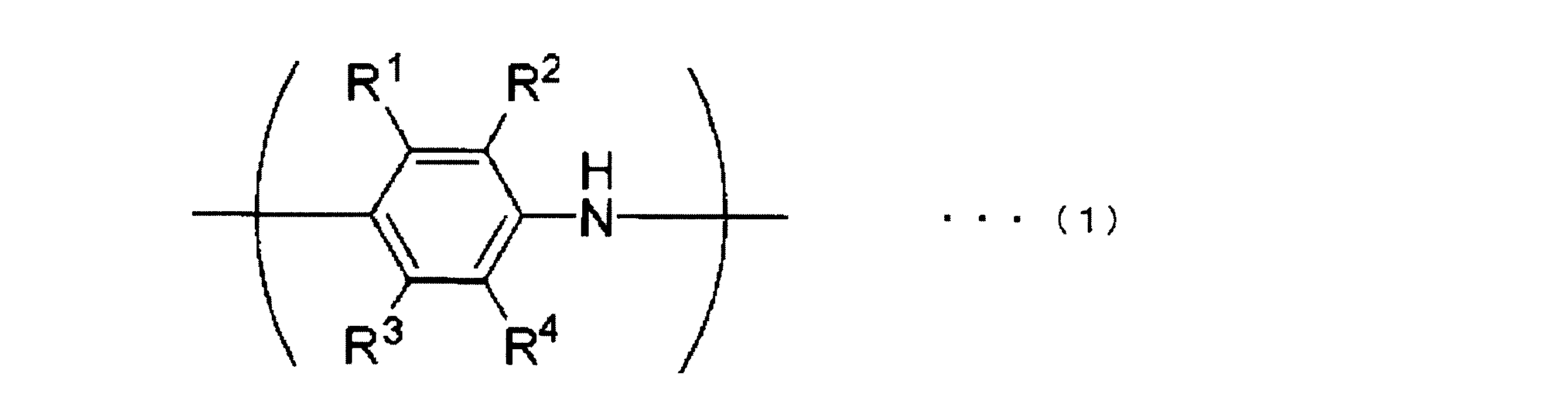
[10] 基材と、前記基材の少なくとも一方の面に[1]~[8]のいずれか1つに記載の導電性組成物から形成された帯電防止膜とを備えた積層体であって、前記帯電防止膜は、350~900nmにおける紫外-可視吸収スペクトルにおいて、450~500nmの波長領域に吸収の極大値を有する、積層体。
[11] 前記帯電防止膜上にレジスト層をさらに備えた、[10]に記載の積層体。
[12] 前記レジスト層上に導電性層をさらに備えた、[11]に記載の積層体。
[13] 前記帯電防止膜側の最表層の表面粗さ(Ra)が1.5nm以下である、[10]~[12]のいずれか1つに記載の積層体。
[14] [1]~[8]のいずれか1つに記載の導電性組成物を基材の少なくとも一方の面に塗布または含浸させた後、80℃以上で加熱処理して帯電防止膜を形成することを含む、積層体の製造方法。
[15] 前記帯電防止膜上にレジスト層を形成する工程をさらに含む、[14]に記載の製造方法。
[16] 前記レジスト層上に導電性層を形成する工程をさらに含む、[15]に記載の製造方法。
[18] [1]~[8]のいずれか1つに記載の導電性組成物を基材の少なくとも一方の面に塗布または含浸させた後、80℃以上で加熱処理して帯電防止膜を形成する工程と、帯電防止膜上にレジスト層を形成する工程と、レジスト層上に導電性層を形成する工程と、導電性層側からレジスト層の表面に電離放射線を照射してパターン描画を行う工程と、パターン描画後に導電性層を除去し、レジスト層を現像してレジストパターンを形成する工程と、前記レジストパターンをマスクとして帯電防止膜をエッチングする工程と、エッチング後に基材上に残存するレジストパターンを除去する工程とを含む、フォトマスクの製造方法。
[19] 前記基材が、前記基材と前記帯電防止膜との界面側に遮光層を有しており、前記エッチングする工程においてさらに遮光層をエッチングすることを含む、[17]または[18]に記載の製造方法。
なお、本発明において「導電性」とは、1010Ω以下の表面抵抗値を有することである。表面抵抗値は、抵抗率計を用い、2端子法(電子間距離20mm)により測定される。
また、本発明において「水溶性」および「可溶性」とは、(i)水、(ii)塩基および/または塩基性塩を含む水、(iii)酸を含む水、または(iv)水と水溶性有機溶剤との混合物10g(液温25℃)のいずれかに、0.1g以上均一に溶解することを意味する。
また、本発明の導電性組成物から形成される塗膜を「帯電防止膜」ともいう。
本発明の導電性組成物は、スルホン酸基および/またはカルボキシ基を有する導電性ポリマー(a)と、少なくとも1つの含窒素複素環およびアミノ基を有する塩基性化合物(b)と、ヒドロキシ基を有する水溶性ポリマー(c)(ただし、前記導電性ポリマー(a)を除く。)と、親水性有機溶剤(d)と、水(e)とを含む。
導電性ポリマー(a)は、スルホン酸基および/またはカルボキシ基(以下、スルホン酸基および/またはカルボキシ基を総称して「酸性基」ともいう。)を有する。ここで、スルホン酸基および/またはカルボキシ基とは、スルホン酸基およびカルボキシ基の少なくとも一方を意味する。
導電性ポリマー(a)としては、スルホン酸基および/またはカルボキシ基を有する高分子化合物であれば特に限定されず、公知の導電性ポリマーを用いることができる。
具体的には、無置換または置換基を有するポリフェニレンビニレン、ポリアセチレン、ポリチオフェン、ポリピロール、ポリアニリン、ポリイソチアナフテン、ポリフラン、ポリカルバゾール、ポリジアミノアントラキノン、およびポリインドールからなる群より選ばれた少なくとも1種のπ共役系導電性ポリマー中の骨格または前記π共役系導電性ポリマー中の窒素原子上に、スルホン酸基および/またはカルボキシ基、あるいは、スルホン酸基および/またはカルボキシ基で置換されたアルキル基またはエーテル結合を含むアルキル基を有している導電性ポリマー、これらのアルカリ金属塩、アンモニウム塩、置換アンモニウム塩が挙げられる。
特に、高い導電性を発現できる観点から、下記一般式(2)~(4)で表される単位からなる群より選ばれた1種以上の単位を、導電性ポリマーを構成する全単位のmol数(100mol%)に対して20~100mol%含有する導電性ポリマーが好ましい。


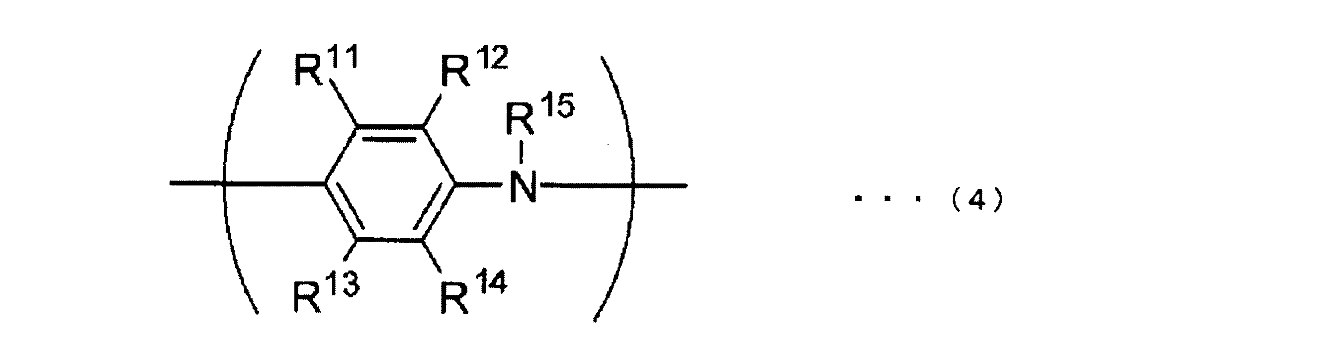
ただし、式(2)のR5~R6のうちの少なくとも1つ、式(3)のR7~R10のうちの少なくとも1つ、式(4)のR11~R15のうちの少なくとも1つは、それぞれ酸性基である。
なお、スルホン酸基には、スルホン酸基を有する置換基(-R17SO3H)も含まれ、アルカリ金属、アンモニウム、または置換アンモニウム等と塩を形成していてもよい。
一方、カルボキシ基には、カルボキシ基を有する置換基(-R17COOH)も含まれ、アルカリ金属、アンモニウム、または置換アンモニウム等と塩を形成していてもよい。
前記R17は炭素数1~24の直鎖もしくは分岐のアルキレン基、アリーレン基またはアラルキレン基を表す。
アルコキシ基としては、例えばメトキシ基、エトキシ基、n-プロポキシ基、iso-プロポキシ基、n-ブトキシ基、iso-ブトキシ基、sec-ブトキシ基、tert-ブトキシ基、ヘプトキシ基、ヘクソオキシ基、オクトキシ基、ドデコキシ基、テトラコソキシ基などが挙げられる。
ハロゲン原子としては、フッ素原子、塩素原子、臭素原子、ヨウ素原子などが挙げられる。
アリール基としては、例えばフェニル基、ナフチル基、トリル基、キシリル基などが挙げられる。
アラルキル基としては、例えばベンジル基、フェネチル基などが挙げられる。
アルキレン基としては、例えばメチレン基、エチレン基、n-プロピレン基、iso-プロピレン基、n-ブチレン基、iso-ブチレン基、sec-ブチレン基、tert-ブチレン基などが挙げられる。
アリーレン基としては、例えばフェニレン基、ナフチレン基などが挙げられる。
アラルキレン基としては、例えばベンジレン基、フェネチレン基などが挙げられる。

また、導電性ポリマー(a)は、導電性に優れる観点で、前記一般式(1)で表される単位を1分子中に10以上含有することが好ましい。
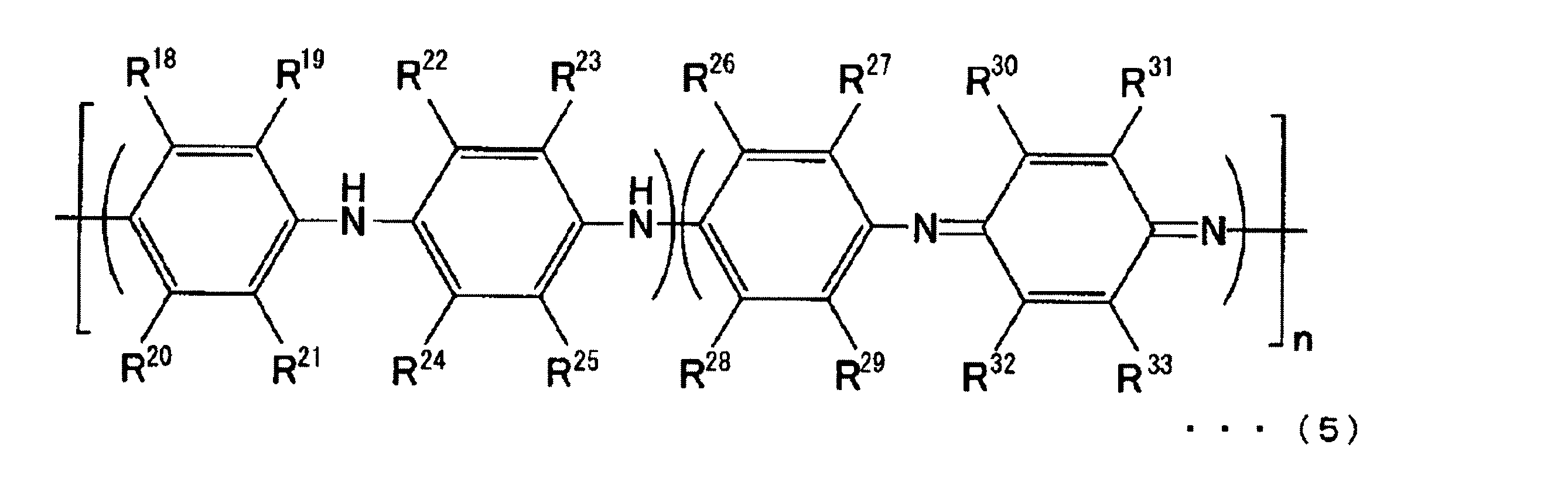
ここで、導電性ポリマー(a)の質量平均分子量は、ゲルパーミエーションクロマトグラフィー(GPC)によって測定される質量平均分子量(ポリスチレンスルホン酸ナトリウム換算)である。
導電性ポリマー(a)は公知の方法で製造できる。例えば、酸性基置換アニリンまたはそのアルカリ金属塩、アンモニウム塩もしくは置換アンモニウム塩を、塩基性反応助剤の存在下、酸化剤を用いて重合することで得られる。
スルホン酸基置換アニリンとして代表的なものは、アミノベンゼンスルホン酸類であり、具体的にはo-,m-もしくはp-アミノベンゼンスルホン酸、アニリン-2,6-ジスルホン酸、アニリン-2,5-ジスルホン酸、アニリン-3,5-ジスルホン酸、アニリン-2,4-ジスルホン酸、アニリン-3,4-ジスルホン酸などが好ましく用いられる。
これらの中では、導電性や溶解性に特に優れる導電性ポリマー(a)が得られる点で、アルキル基置換アミノベンゼンスルホン酸類、アルコキシ基置換アミノベンゼンスルホン酸類、ヒドロキシ基置換アミノベンゼンスルホン酸類、または、ハロゲン置換アミノベンゼンスルホン酸類が好ましく、製造が容易な点で、アルコキシ基置換アミノベンゼンスルホン酸類、そのアルカリ金属塩、アンモニウム塩または置換アンモニウム塩がより好ましく、2-アミノ-4-メトキシベンゼンスルホン酸、3-アミノ-4-メトキシベンゼンスルホン酸が特に好ましい。
これらのスルホン酸基置換アニリンはそれぞれ1種単独で用いてもよいし、2種以上を任意の割合で混合して用いてもよい。
塩基性反応助剤としては無機塩基が好ましく、具体的には水酸化ナトリウム、水酸化カリウム、水酸化リチウムなどが挙げられる。
また、無機塩基以外では、メチルアミン、ジメチルアミン、トリメチルアミン、エチルアミン、ジエチルアミン、トリエチルアミン、エチルメチルアミン、エチルジメチルアミン、ジエチルメチルアミン等の脂式アミン類;ピリジン、α-ピコリン、β-ピコリン、γ-ピコリン等の環式不飽和アミン類が、塩基性反応助剤として好ましく用いられる。
これらの塩基性反応助剤はそれぞれ1種単独で用いてもよいし、2種以上を任意の割合で混合して用いてもよい。
これらの酸化剤はそれぞれ1種単独で用いてもよいし、2種以上を任意の割合で混合して用いてもよい。
反応時間は1分~5時間が好ましい。
反応温度は-15~60℃が好ましい。
なお、溶媒として混合溶媒を用いる場合、水と水溶性有機溶媒との混合比は任意であるが、水:水溶性有機溶媒=1:100~100:1が好ましい。
イオン交換法を用いることにより、導電性ポリマーの酸性基と塩を形成した状態で存在する塩基性物質や、酸性物質などを効果的に除去でき、純度の高い導電性ポリマー(a)を得ることができる。
なお、イオン交換法で酸性物質や塩基性物質等を除去する場合は、重合で得られた反応混合物を所望の濃度になるように水性媒体に溶解させ、反応混合物溶液としてから酸性物質や塩基性物質等を除去する。
水性媒体としては、水、水溶性有機溶剤、水と水溶性有機溶剤との混合溶剤が挙げられる。水溶性有機溶剤は、水に可溶な有機溶剤であり、例えばメタノール、エタノール、イソプロピルアルコール、n-プロピルアルコール、1-ブタノール等のアルコール類;アセトン、メチルエチルケトン、エチルイソブチルケトン、メチルイソブチルケトン等のケトン類;エチレングリコール、エチレングリコールメチルエーテル、エチレングリコールモノ-n-プロピルエーテル等のエチレングリコール類;プロピレングリコール、プロピレングリコールメチルエーテル、プロピレングリコールエチルエーテル、プロピレングリコールブチルエーテル、プロピレングリコールプロピルエーテル等のプロピレングリコール類;ジメチルホルムアミド、ジメチルアセトアミド等のアミド類;N-メチルピロリドン、N-エチルピロリドン等のピロリドン類;乳酸メチル、乳酸エチル、β-メトキシイソ酪酸メチル、α-ヒドロキシイソ酪酸メチル等のヒドロキシエステル類などが挙げられる。
なお、精製後の導電性ポリマー(a)は、水などの水性媒体に分散または溶解した状態である。従って、エバポレータなどで水性媒体を全て除去すれば固体状の導電性ポリマー(a)が得られるが、導電性ポリマー(a)は溶剤に分散または溶解した状態のまま導電性組成物の製造に用いてもよい。
塩基性化合物(b)は、少なくとも1つの含窒素複素環およびアミノ基を有する。塩基性化合物(b)を用いると、分子中の複数の塩基点が導電性ポリマー(a)中の酸性基へ効率良く作用することで架橋状態が形成されると考えられ、その結果、水やアルカリ性溶液等の溶剤に対する耐性(以下、「耐溶剤性」という。)が向上する。しかも、ガラス基材やタンタル基材等の基材に対する密着性(以下、「基材密着性」という。)も向上する。
これらの塩基性化合物(b)はそれぞれ1種単独で用いてもよいし、2種以上を任意の割合で混合して用いてもよい。
水溶性ポリマー(c)は、ヒドロキシ基を有する。
水溶性ポリマー(c)を用いると、分子中のヒドロキシ基が導電性ポリマー(a)中の酸性基と反応してエステル結合が形成されると考えられ、その結果、導電性ポリマー(a)が不溶化し、帯電防止膜の耐溶剤性が向上する。加えて、基材密着性も向上する。
これらの水溶性ポリマー(c)はそれぞれ1種単独で用いてもよいし、2種以上を任意の割合で混合して用いてもよい。
親水性有機溶剤(d)としては、導電性ポリマー(a)、塩基性化合物(b)、および水溶性ポリマー(c)を溶解することができる有機溶剤であれば、本発明の効果を有する限り特に限定はされないが、例えば、メタノール、エタノール、n-プロピルアルコール、イソプロピルアルコール、ブタノール等のアルコール類;アセトン、エチルイソブチルケトン等のケトン類;エチレングリコール、エチレングリコールメチルエーテル等のエチレングリコール類;プロピレングリコール、プロピレングリコールメチルエーテル、プロピレングリコールエチルエーテル、プロピレングリコールブチルエーテル、プロピレングリコールプロピルエーテル等のプロピレングリコール類;ジメチルホルムアミド、ジメチルアセトアミド等のアミド類;N-メチルピロリドン、N-エチルピロリドン等のピロリドン類などが挙げられる。これらの中でも、帯電防止膜や、前記帯電防止膜上にレジスト層が形成された積層体の表面平滑性が向上する点で、炭素数1~3の1価のアルコール、例えばメタノール、エタノール、n-プロピルアルコール、イソプロピルアルコールがより好ましく、メタノール、エタノール、イソプロピルアルコールが特に好ましい。
これらの親水性有機溶剤(d)はそれぞれ1種単独で用いてもよいし、2種以上を任意の割合で混合して用いてもよい。
導電性組成物中の水(e)と親水性有機溶剤(d)との質量比は、水(e)/親水性有機溶剤(d)=1/100~100/1であることが好ましく、2/100~100/2であることがより好ましい。
導電性組成物は、本発明の効果を損なわない範囲内であれば、添加剤をさらに含んでいてもよい。
添加剤としては、任意の公知の塗料に用いられる添加剤が挙げられ、例えば、顔料、消泡剤、紫外線吸収剤、酸化防止剤、耐熱性向上剤、レベリング剤、たれ防止剤、艶消し剤、防腐剤などが挙げられる。
導電性組成物は、上述した導電性ポリマー(a)と、塩基性化合物(b)と、水溶性ポリマー(c)と、親水性有機溶剤(d)と、水(e)とを混合して製造することができる。
混合時の温度は、0~100℃が好ましく、10~90℃がより好ましい。混合時の温度が上記範囲内であれば、導電性ポリマー(a)、塩基性化合物(b)および水溶性ポリマー(c)が親水性有機溶剤(d)および水(e)に溶解しやすい。また、水溶性ポリマー(c)は、マイクロゲルを生じやすい傾向にある。マイクロゲルが生じると帯電防止膜の平滑性が低下する傾向にある。混合時の温度が上記範囲内であれば、導電性組成物中でマイクロゲルを生じにくくすることもできる。
以上説明した本発明の導電性組成物は、上述した導電性ポリマー(a)と、塩基性化合物(b)と、水溶性ポリマー(c)と、親水性有機溶剤(d)と、水(e)とを含むので、耐溶剤性および基材密着性に優れた帯電防止膜を形成できる。耐溶剤性および基材密着性に優れた帯電防止膜を形成できる理由は、以下のように考えられる。
導電性ポリマー(a)と、塩基性化合物(b)と、水溶性ポリマー(c)とを併用すると、導電性ポリマー(a)中の酸性基と塩基性化合物(b)の塩基点(窒素含有複素環およびアミノ基)とが架橋するとともに、導電性ポリマー(a)中の酸性基と水溶性ポリマー(c)中のヒドロキシ基とがエステル結合を形成し、その結果、帯電防止膜の耐溶剤性および基材密着性が向上すると考えられる。
なお、親水性有機溶剤(d)および水(e)は、導電性組成物での導電性ポリマー(a)と、塩基性化合物(b)と、水溶性ポリマー(c)とによる上記架橋反応やエステル反応を抑制する役割を果たしている。そのため、導電性組成物の状態では、架橋反応やエステル反応は起こりにくく、安定した状態を維持できる。導電性組成物を後述する基材上に塗布または含浸させ、加熱処理することで親水性有機溶剤(d)および水(e)が除去されると、架橋反応やエステル反応が進行して、耐溶剤性および基材密着性に優れた帯電防止膜が得られる。
導電性組成物は、前記導電性組成物の総質量に対して、導電性ポリマー(a)を0.01~15質量%、親水性有機溶剤(d)を1~15質量%含み、前記導電性ポリマー(A)1molに対して、塩基性化合物(b)を0.01~1mol不含み、導電性ポリマー(a)100質量部に対して水溶性ポリマー(c)を0.01~100質量部含み、水(e)/親水性有機溶剤(d)=1/100~100/1となる量の水(e)を含むことが好ましい。
本発明の導電性組成物の用途としては、レジスト層の下層膜として用いる帯電防止膜、コンデンサ、透明電極、半導体材料などが挙げられる。特に、帯電防止膜や、前記帯電防止膜を備えた積層体に好適に用いられる。
本発明の帯電防止膜は、上述した本発明の導電性組成物から形成される。具体的には、導電性組成物を基材上に塗布または含浸させ、加熱することで得られる。
帯電防止膜は、350~900nmにおける紫外-可視吸収スペクトルにおいて、450~500nmの波長領域に吸収の極大値を有する。
帯電防止膜の厚さは、任意の5箇所について、段差計を用いて測定し、これらの値を平均したものである。
加えて、本発明の帯電防止膜は、基材、より好ましくはガラス基材、タンタル基材等の基材との密着性にも優れる。
特に、導電性組成物が親水性有機溶剤(d)として炭素数1~3の1価のアルコールを含んでいれば、帯電防止膜の表面平滑性も向上し、具体的には、帯電防止膜の表面粗さ(Ra)が1.5nm以下となりやすい。帯電防止膜の表面粗さ(Ra)は1.0nm以下が好ましい。また、帯電防止膜の表面粗さ(Ra)の1つの側面としては、0.3nm以上である。
<第一の態様>
図1に、本発明の第一の態様の積層体の一例を示す。
この例の積層体10は、基材11と、前記基材11の一方の面に形成された帯電防止膜12とを備えている。
また、前記ガラス、石英ガラス、ソーダライムガラス等の基材本体の表面に、クロムなどの金属等からなる遮光層が形成されたものを基材として用いてもよい。また、これら基材の表面には、各種塗料や感光性樹脂、レジスト等がコーティングされていてもよい。
帯電防止膜12の厚さは、5~1000nmが好ましく、5~500nmがより好ましい。
帯電防止膜12の厚さは、任意の5箇所について、段差計を用いて測定し、これらの値を平均したものである。
また、本発明の導電性組成物は、耐溶剤性、塗布性が良好であるので、上記基材上に各種塗料や感光性材料をコーティングしたものに、導電性組成物を重ね塗りして塗膜を形成すること、あるいは、上記基材上に導電性組成物を塗り、塗膜(帯電防止膜)を形成したものに、各社塗料や、感光性材料をコーティングすることも可能である。
加熱処理温度は、80℃以上が好ましく、100℃以上がより好ましく、130℃以上がさらに好ましく、200℃以上が特に好ましい。加熱処理温度が高くなるほど、導電性ポリマー(a)中の酸性基と水溶性ポリマー(c)中のヒドロキシ基との反応が促進されてエステル結合が形成されやすくなり、不溶性の塗膜(帯電防止膜)が形成されやすくなる傾向にある。これにより、永久帯電防止膜、およびプロセス上の一時的帯電防止膜の両面での適用が可能となるという利点を有する。特に、加熱処理温度が130℃以上であれば、帯電防止膜の耐溶剤性がより向上する。加熱処理温度は400℃以下が好ましい。
加熱処理時間は、2分間以上が好ましい。
加熱処理は、2段階以上に分けて行ってもよい。例えば、80℃以上130℃未満で加熱処理(第一の加熱処理)した後、130℃以上で加熱処理(第二の加熱処理)してもよい。
加えて、積層体は、基材、より好ましくはガラス基材、タンタル基材等の基材と帯電防止膜との密着性にも優れる。
特に、導電性組成物が親水性有機溶剤(d)として炭素数1~3の1価のアルコールを含んでいれば、積層体の表面平滑性も向上し、具体的には、帯電防止膜側の最表層の表面粗さ(Ra)が1.5nm以下となりやすい。前記最表層の表面粗さ(Ra)は1.0nm以下が好ましい。また、前記最表層の表面粗さ(Ra)の1つの側面としては、0.3nm以上である。
図2に、本発明の第二の態様の積層体の一例を示す。
この例の積層体20は、基材11と、前記基材11の少なくとも一方の面に形成された帯電防止膜12と、前記帯電防止膜12上に形成されたレジスト層13とを備えている。
なお、図2および後述の図3、4において、図1と同じ構成要素には同じ符号を付してその説明を省略する。
レジスト層13の厚さは、10~10000nmが好ましく、10~5000nmがより好ましい。
レジスト層13の厚さは、任意の3箇所について、段差計を用いて測定し、これらの値を平均したものである。
また、図2に示す積層体20、図3に示す積層体30、図4に示す積層体40は、基材11の一方の面に帯電防止膜12が形成されているが、基材11の他方の面にも帯電防止膜12が形成されていてもよい。
導電性層14の厚さは、任意の3箇所について、段差計を用いて測定し、これらの値を平均したものである。
加えて、積層体は、基材、より好ましくはガラス基材、タンタル基材等の基材と帯電防止膜との密着性にも優れる。
特に、導電性組成物が親水性有機溶剤(d)として炭素数1~3の1価のアルコールを含んでいれば、積層体の表面平滑性も向上し、具体的には、帯電防止膜側の最表層の表面粗さ(Ra)が1.5nm以下となりやすい。前記最表層の表面粗さ(Ra)は1.0nm以下が好ましい。また、前記最表層の表面粗さ(Ra)の1つの側面としては、0.3nm以上である。
ところで、レジスト層への電離放射線の照射によりレジスト層上に電子が蓄積すると、反発により電離放射線が曲がり、レジスト層に入射する電子の位置がずれることがある。レジスト層上に導電性層が形成されていれば、レジスト層上の帯電を防止できるので、パターン描画の精度の低下をより抑制でき、目的とするレジストパターンに対応する潜像をより精度よく形成できる。
よって、本発明の第二の態様の積層体は、フォトマスク用の材料(マスクブランクス)として好適である。
<第三の態様>
本発明の第三の態様のフォトマスクの製造方法は、帯電防止膜形成工程と、レジスト層形成工程と、露光工程と、現像工程と、エッチング工程と、レジスト除去工程とを含む。
基材としては、積層体の説明において先に例示した各種基材を用いることができる。これらの中でも、ガラス、石英ガラスなどが好適であり、石英ガラス、またはクロムなどの金属等からなる遮光層が表面に形成された石英ガラスがより好適である。
導電性組成物の基材への塗布方法または含浸方法としては、本発明の第一の態様の積層体の説明において先に例示した、導電性組成物の基材への塗布方法または含浸方法が挙げられる。
加熱処理温度は、80℃以上が好ましく、100℃以上がより好ましく、130℃以上がさらに好ましく、200℃以上が特に好ましい。加熱処理温度は、400℃以下が好ましい。
また、帯電防止膜形成工程では、導電性組成物を基材の少なくとも一方の面に塗布または含浸させた後、加熱処理を2段階以上に分けて行ってもよい。例えば、80℃以上130℃未満で加熱処理(第一の加熱処理)した後、130℃以上で加熱処理(第二の加熱処理)してもよい。
レジスト層を構成するレジスト、およびレジスト層を形成する方法としては、本発明の第二の態様の積層体の説明において先に例示したレジスト、およびレジスト層の形成方法が挙げられる。
電離放射線としては、電子線、X線、ガンマ線などが挙げられる。
電離放射線の照射の方法としては、それ自体公知の方法を採用できる。
現像液としては、レジスト層の現像に用いられる公知の現像液を使用できるが、例えば、レジストを構成するレジストが化学増幅型のレジストであれば、水酸化テトラメチルアンモニウム水溶液等のアルカリ現像液などが挙げられ、非化学増幅型のレジストであれば、酢酸アミルやメチルエチルケトン等の有機現像液などが挙げられる。
現像後に、必要に応じてリンス処理を行ってもよい。
エッチングの方法としてはそれ自体公知の方法を採用できるが、例えばドライエッチング、ウエットエッチングなどが挙げられる。
基材として、帯電防止膜が形成される側の面に遮光層が形成されているものを用いる場合は、エッチングによりレジストパターンでマスクされていない部分の帯電防止膜および遮光層が除去される。
レジストパターンの除去には、それ自体公知の剥離剤を用いることができる。
また、レジスト層の下層に帯電防止膜を形成することで、帯電防止膜からアースをとることができる。よって、チャージアップによりレジスト層に入射する電子の位置がずれてパターン描画の精度が低下することを抑制できる。基材と帯電防止膜との間に遮光層が形成されている場合は、帯電防止膜によって遮光層の静電破壊等を防止することもできる。一方、遮光層がなくても、前記帯電防止膜を有することにより、十分な導電性を発現できる。
よって、本発明の第三の態様のフォトマスクの製造方法によれば、高精度なパターンが形成されたフォトマスクを製造できる。
本発明の第四の態様のフォトマスクの製造方法は、帯電防止膜形成工程と、レジスト層形成工程と、導電性層形成工程と、露光工程と、除去・現像工程と、エッチング工程と、レジスト除去工程とを含む。
本発明の第四の態様のフォトマスクの製造方法において、導電性層形成工程および除去・現像工程以外は、本発明の第三の態様のフォトマスクの製造方法と同じである。なお、露光工程では、導電性層側からレジスト層の表面に電離放射線を照射する。
導電性層を構成する材料、および導電性層を形成する方法としては、本発明の第二の態様の積層体の説明において先に例示した導電性層を構成する材料、および導電性層の形成方法が挙げられる。
導電性層を構成する材料が、導電性高分子の溶液、イオン性の導電性を有する化合物の場合、これらは水溶性であるため、水洗により導電性層を溶解除去できる。水洗は、水性液に接触させることを示す。水性液としては、水、塩基および/または塩基性塩を含む水、酸を含む水、水と水溶性有機溶媒との混合物等が挙げられる。一方、導電性層を構成する材料が金属の場合、エッチングにより導電性層を除去できる。
レジスト層の現像は、本発明の第一の態様のフォトマスクの製造方法の説明において先に例示した現像工程と同様の操作を行えばよい。
方法(i):導電性層の除去と、レジスト層の現像を同時に行う。
方法(ii):導電性層を除去した後に、レジスト層の現像を行う。
方法(ii)の場合、上述した方法により導電性層を除去した後、レジスト層を現像する。水洗により導電性層を除去する場合、水洗には現像液に該当しない水性液、例えば水等を用いて導電性層を除去する。
また、レジスト層の下層に帯電防止膜を形成することで、帯電防止膜からアースをとることができる。よって、チャージアップによりレジスト層に入射する電子の位置がずれてパターン描画の精度が低下することを抑制できる。基材と帯電防止膜との間に遮光層が形成されている場合は、帯電防止膜によって遮光層の静電破壊等を防止することもできる。一方、遮光層がなくても、前記帯電防止膜を有することにより、十分な導電性を発現できる。
また、レジスト層上に導電性層を形成するので、レジスト層上の帯電を防止できる。従って、パターン描画の精度の低下をより抑制でき、目的とするレジストパターンに対応する潜像をより精度よく形成できる。
よって、本発明の第四の態様のフォトマスクの製造方法によれば、高精度なパターンが形成されたフォトマスクを製造できる。
なお、実施例および比較例における各種測定・評価方法は以下の通りである。
(分子量の測定)
水溶性ポリマー(c)の0.1質量%水溶液を、0.45μmのメンブレンフィルターにて濾過し、サンプル調整を行なった。前記サンプルのゲルパーミエーションクロマトグラフィー(GPC)測定を以下の条件で行い、水溶性ポリマー(c)の質量平均分子量を測定した。
測定機:TOSOH GPC-8020(東ソー株式会社製)
溶離液:0.2M―NaNO3-DIW/アセトニトリル=80/20(v/v)
カラム温度:30℃
検量線:EasiVialTMポリエチレングリコール/オキシド(PolymerLab社製)を用いて作成
導電性組成物を目視にて観察し、以下の評価基準にて配合安定性を評価した。
○:凝集物が認められない。
×:凝集物が認められる。
ガラス基材上に、導電性組成物をスピンコート塗布(2000rpm×60秒間)した後、ホットプレートにて80℃で2分間、150℃で30分間、または200℃で30分間加熱処理を行い、膜厚約50nmの塗膜がガラス基材上に形成された導電体(積層体)を作製した。
得られた導電体の表面抵抗値[Ω]を、抵抗率計(三菱化学株式会社製、「ハイレスタMCP-HT260」)を用い、2端子法(電極間距離20mm)にて測定した。
ガラス基材上に、導電性組成物をスピンコート塗布(2000rpm×60秒間)した後、ホットプレートにて80℃で2分間加熱処理を行い、その後、200℃で30分間さらに加熱処理を行い、膜厚約50nmの塗膜がガラス基材上に形成された導電体(積層体)を作製した。塗膜表面の状態を目視にて観察し、以下の評価基準にて塗膜安定性を評価した。
○:ひび割れが認められない。
×:ひび割れが認められる。
ガラス基材上に、導電性組成物をスピンコート塗布(2000rpm×60秒間)した後、ホットプレートにて80℃で2分間加熱処理を行い、その後、200℃で30分間さらに加熱処理を行い、膜厚約50nmの塗膜がガラス基材上に形成された導電体(積層体)を作製した。ついで得られた塗膜をガラス基材ごと各溶剤(水、アセトン、アルカリ性溶液)に10分間浸した。その後、水洗し、さらに風乾して、塗膜の溶解(溶出)の具合を目視にて観察し、以下の評価基準にて各溶剤に対する耐性(耐溶剤性)を評価した。なお、アルカリ性溶液としては、2.38質量%水酸化テトラメチルアンモニウム(TMAH)水溶液を用いた。
○:溶出が認められない。
△:塗膜の一部が溶出している。
×:塗膜が完全に溶出している。
各基材(ガラス、マスクブランクス、タンタル)上に、導電性組成物0.1mLを滴下した後、オーブンにて200℃で10分間加熱処理を行い、塗膜を得た。得られた塗膜を基材ごと水に10分間浸した。その後、風乾して、塗膜の剥離の具合を目視にて観察し、以下の評価基準にて各基材に対する密着性(基材密着性)を評価した。なお、マスクブランクスとしては、石英ガラスの一方の面に、クロム薄膜が形成されたものを用い、前記クロム薄膜上に導電性組成物を滴下して塗膜を形成した。
○:剥離が認められない。
△:塗膜の一部が剥離している。
×:塗膜が完全に剥離している。
4inchシリコンウエハ上に、導電性組成物をスピンコート塗布(2000rpm×60秒間)した後、オーブンにて200℃で30分間加熱処理を行い、膜厚約50nmの塗膜を形成した。前記塗膜上に電子線レジスト(富士フイルム株式会社製、「FEP-717」)を塗布して乾燥させ、シリコンウエハ上に塗膜およびレジスト層が順次形成された積層体を作製した。
得られた積層体のレジスト層側の表面粗さ(Ra)を段差・表面あらさ・微細形状測定装置(ケーエルエー・テンコール株式会社製、「プロファイラーP-16」)にて測定し、以下の評価基準にて表面平滑性を評価した。Raが小さいほど、表面平滑性に優れることを意味する。
〇:Raが1.0nm以下である。
○△:Raが1.0nm超、1.5nm以下である。
×:Raが1.5nm超である。
(導電性ポリマー(a)の水溶液(a-1)の製造)
3-アミノアニソール-4-スルホン酸1molを、4mol/L濃度のピリジン溶液(溶媒:水/アセトニトリル=3/7)300mLに0℃で溶解し、モノマー溶液を得た。別途、ペルオキソ二硫酸アンモニウム1molを、水/アセトニトリル=3/7の溶液1Lに溶解し、酸化剤溶液を得た。ついで、酸化剤溶液を5℃に冷却しながら、モノマー溶液を滴下した。滴下終了後、25℃で12時間さらに攪拌して、導電性ポリマーを得た。その後、得られた導電性ポリマーを含む反応混合物を遠心濾過器にて濾別した。さらに、メタノールにて洗浄した後乾燥させ、粉末状の導電性ポリマー(a-1-1)を185g得た。
得られた導電性ポリマー(a-1-1)40gを、超純水960gに溶解させ、濃度4質量%の導電性ポリマー(a)の水溶液(a-1-2)を1000g得た。
超純水により洗浄した陽イオン交換樹脂(オルガノ株式会社製、「アンバーライトIR-120B(H)」)500mLをカラムに充填した。
このカラムに、導電性ポリマー(a)の水溶液(a-1-2)1000gを、50mL/分(SV=6[1/h])の速度で通過させて、塩基性物質等が除去された導電性ポリマー(a)の水溶液(a-1-3)を900g得た。
次に、超純水により洗浄した陰イオン交換樹脂(オルガノ株式会社製、「アンバーライトIRA410」)500mLをカラムに充填した。
このカラムに、導電性ポリマー(a)の水溶液(a-1-3)900gを、50mL/分(SV=6)の速度で通過させて、塩基性物質等が除去された導電性ポリマー(a)の水溶液(a-1)を800g得た。
この導電性ポリマー(a)の水溶液(a-1)についてイオンクロマトグラフィにより組成分析を行なったところ、残存モノマーは60%、硫酸イオンは99%、塩基性物質は99%以上除去されていた。
なお、SV=(カラムへの通液流量)/(カラムに充填した樹脂量)と定義される。
(水溶性ポリマー(c)の水溶液(c-1)の製造)
ポリビニルアルコール(株式会社クラレ製、「エクセバールRS-4104」、ケン化度98~99%)20gを超純水980gに溶解させ、95℃で2時間、加熱撹拌し、濃度2質量%の水溶性ポリマー(c)の水溶液(c-1)を1000g得た。
(水溶性ポリマー(c)の水溶液(c-2)の製造)
ビニルモノマーとしてN-ビニル-2-ピロリドン55gと、重合開始剤としてアゾビスイソブチロニトリル1gと、末端疎水性基導入のための連鎖移動剤としてn-オクタデシルメルカプタン0.16gとを、溶剤であるイソプロピルアルコール100mLに攪拌溶解して反応溶液を得た。その後、予め80℃に加熱しておいたイソプロピルアルコール中に、前記反応溶液を1mL/分の滴下速度で滴下し、滴下重合を行った。滴下重合は、イソプロピルアルコールの温度を80℃に保ちながら行った。滴下終了後、80℃でさらに2時間熟成した後、放冷した。その後、減圧濃縮を行い、得られた反応物を少量のアセトンに再溶解させた。この反応物のアセトン溶液を、過剰のn-ヘキサンに滴下することで得られた白色沈殿を濾別し、n-ヘキサンで洗浄した後乾燥させ、45gの水溶性ポリマー(c-2-1)を得た。得られた水溶性ポリマー(c-2-1)の質量平均分子量は4800であった。
得られた水溶性ポリマー(c-2-1)50gを超純水950gに溶解させ、濃度5質量%の水溶性ポリマー(c)の水溶液(c-2)を1000g得た。
表1~3に示す配合組成にて導電性ポリマー(a)の水溶液と、塩基性化合物(b)の溶液と、水溶性ポリマー(c)の水溶液と、親水性有機溶剤(d)と、水(e)とを25℃で混合し、導電性組成物を調製した。なお、表1~3中の水(e)の量(質量部)には、導電性ポリマー(a)の水溶液、塩基性化合物(b)の溶液、および水溶性ポリマー(c)の水溶液中の水の量は含まれない。
得られた導電性組成物を用い、配合安定性、導電性、塗膜安定性、耐溶剤性、基材密着性、表面平滑性を評価した。結果を表1~3に示す。

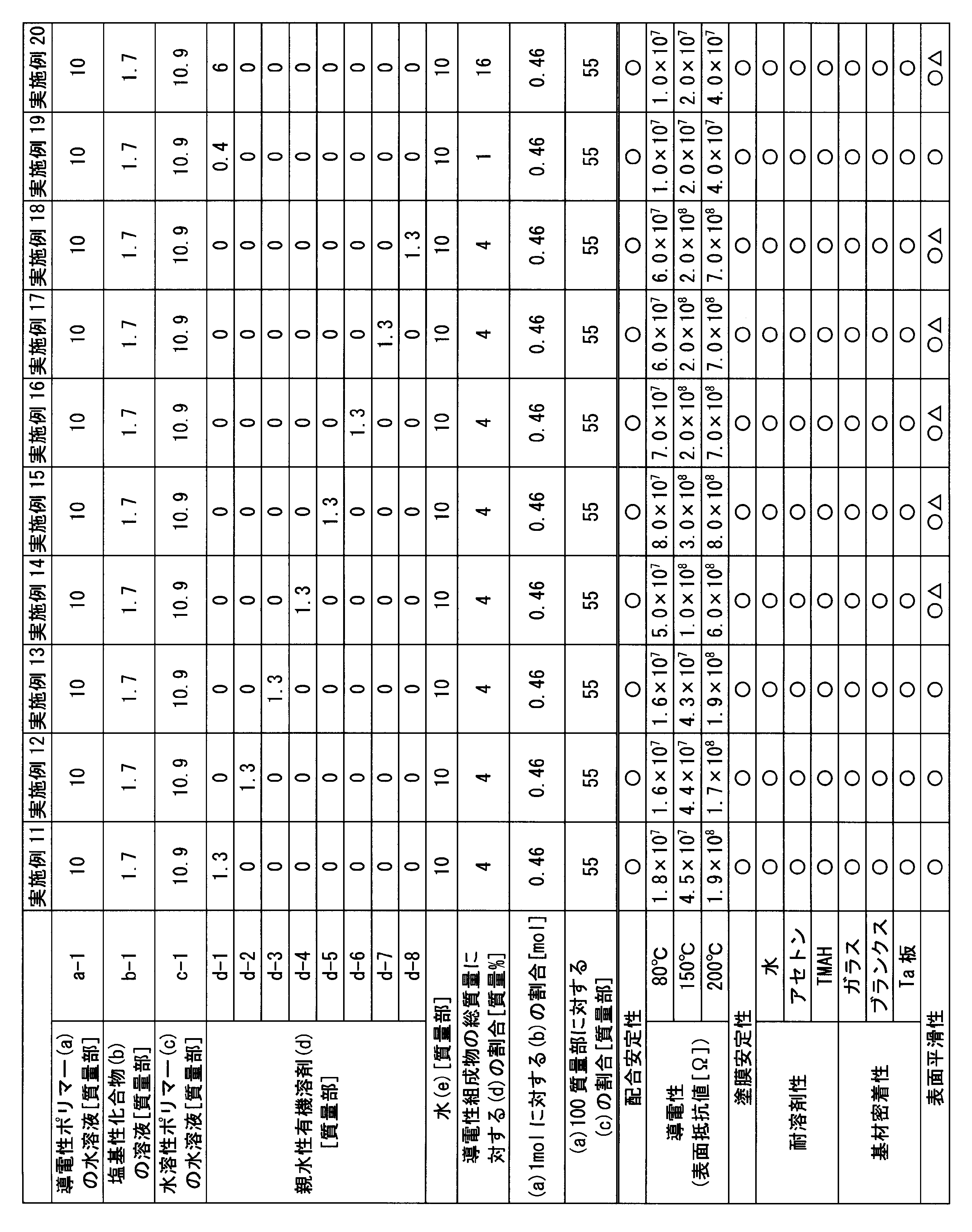
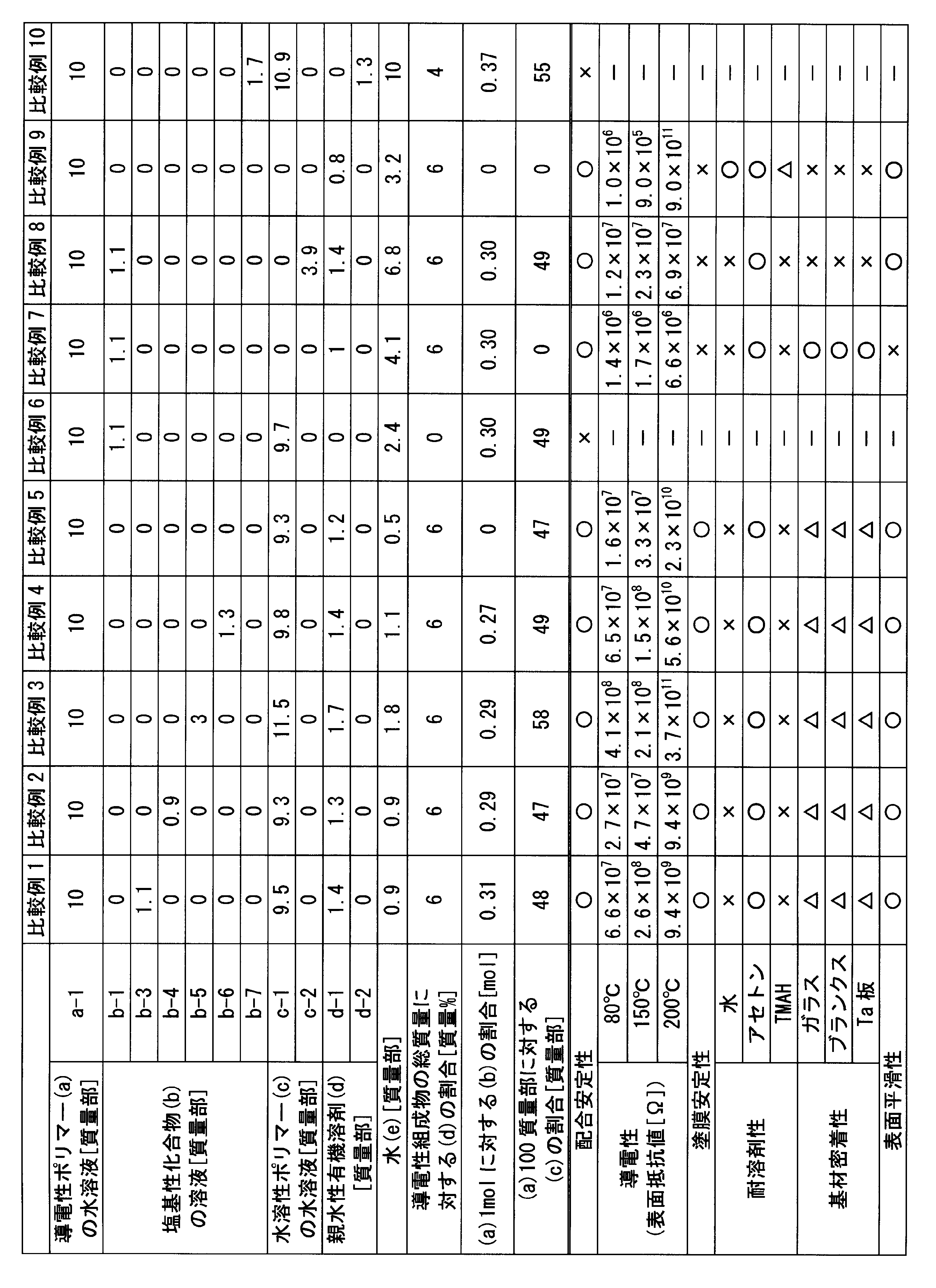

b-1:4-アミノピリジンの5質量%水溶液、
b-2:3,4-ジアミノピリジンの3質量%イソプロピルアルコール溶液、
b-3:水酸化テトラエチルアンモニウムの5質量%水溶液、
b-4:ピリジンの5質量%水溶液、
b-5:水酸化テトラブチルアンモニウムの5質量%水溶液、
b-6:トリス(ヒドロキシメチル)アミノメタンの5質量%水溶液、
b-7:ジアミノヘキサンの5質量%水溶液、
d-1:イソプロピルアルコール、
d-2:メタノール、
d-3:エタノール、
d-4:ブタノール、
d-5:アセトン、
d-6:グリセリン、
d-7:ジエチレングリコール、
d-8:プロピレングリコールモノメチルエーテルアセテート、
ブランクス:クロム薄膜が石英ガラスに形成された、マスクブランクス、
Ta板:純度99.95%のタンタル板。
塩基性化合物(b)の溶液を用いていない比較例5の導電性組成物は、水およびアルカリ性溶液に対する耐性に劣り、各種基材に対する密着性も乏しかった。
親水性有機溶剤(d)を用いていない比較例6の導電性組成物は、配合直後に凝集物が析出し、塗膜を形成することができなかった。
水溶性ポリマー(c)の水溶液を用いていない比較例7の導電性組成物は、加熱処理後の膜表面が荒れており、水およびアルカリ性溶液に対する耐性に劣っていた。また、表面平滑性にも劣っていた。
ヒドロキシ基を有さない水溶性ポリマーの水溶液(c-2)を用いた比較例8の導電性組成物は、加熱処理後の膜表面が荒れており、水およびアルカリ性溶液に対する耐性に劣っていた。また、各種基材に対する密着性も乏しかった。
塩基性化合物(b)の溶液および水溶性ポリマー(c)の水溶液を用いていない比較例9の導電性組成物は、加熱後の膜表面が荒れていた。また、各種基材に対する密着性も乏しかった。
ジアミノヘキサンの5質量%水溶液(b-7)を用いた比較例10の導電性組成物は、配合直後に凝集物が析出し、塗膜を形成することができなかった。
一方、比較例9の導電性組成物から形成される塗膜は、加熱処理温度が80℃の場合は、350~900nmにおける紫外-可視吸収スペクトルにおいて、450~500nmの波長領域に吸収の極大値を有していたが、加熱処理温度が200℃に上がると、吸収の極大値が消失した。また、加熱処理温度が80℃の場合、水およびアルカリ性溶液に対する耐性に劣っていた。
11 基材
11a 基材本体
11b 遮光層
12 帯電防止膜
13 レジスト層
14 導電性層
20 積層体
30 積層体
40 積層体
Claims (19)
- スルホン酸基および/またはカルボキシ基を有する導電性ポリマー(a)と、少なくとも1つの含窒素複素環およびアミノ基を有する塩基性化合物(b)と、ヒドロキシ基を有する水溶性ポリマー(c)(ただし、前記導電性ポリマー(a)を除く。)と、親水性有機溶剤(d)と、水(e)とを含む、導電性組成物。
- 前記塩基性化合物(b)が共役構造を有する、請求項1に記載の導電性組成物。
- 前記含窒素複素環がピリジン環である、請求項1または2に記載の導電性組成物。
- 前記水溶性ポリマー(c)がポリビニルアルコールである、請求項1~3のいずれか一項に記載の導電性組成物。
- 前記ポリビニルアルコールのケン化度が85%以上である、請求項4に記載の導電性組成物。
- 前記親水性有機溶剤(d)が炭素数1~3の1価のアルコールである、請求項1~5のいずれか一項に記載の導電性組成物。
- 前記導電性組成物の総質量に対して、前記親水性有機溶剤(d)の含有量が1~15質量%である、請求項1~6のいずれか一項に記載の導電性組成物。
- 前記導電性ポリマー(a)が下記一般式(1)で表される単位を有する、請求項1~7のいずれか一項に記載の導電性組成物。

式(1)中、R1~R4は、各々独立に、水素原子、炭素数1~24の直鎖もしくは分岐のアルキル基、炭素数1~24の直鎖もしくは分岐のアルコキシ基、酸性基、ヒドロキシ基、ニトロ基、またはハロゲン原子であり、R1~R4のうちの少なくとも1つは酸性基であり、前記酸性基はスルホン酸基またはカルボキシ基である。 - 請求項1~8のいずれか一項に記載の導電性組成物から形成された帯電防止膜であって、
350~900nmにおける紫外-可視吸収スペクトルにおいて、450~500nmの波長領域に吸収の極大値を有する、帯電防止膜。 - 基材と、前記基材の少なくとも一方の面に請求項1~8のいずれか一項に記載の導電性組成物から形成された帯電防止膜とを備えた積層体であって、
前記帯電防止膜は、350~900nmにおける紫外-可視吸収スペクトルにおいて、450~500nmの波長領域に吸収の極大値を有する、積層体。 - 前記帯電防止膜上にレジスト層をさらに備えた、請求項10に記載の積層体。
- 前記レジスト層上に導電性層をさらに備えた、請求項11に記載の積層体。
- 前記帯電防止膜側の最表層の表面粗さ(Ra)が1.5nm以下である、請求項10~12のいずれか一項に記載の積層体。
- 請求項1~8のいずれか一項に記載の導電性組成物を基材の少なくとも一方の面に塗布または含浸させた後、80℃以上で加熱処理して帯電防止膜を形成することを含む、積層体の製造方法。
- 前記帯電防止膜上にレジスト層を形成する工程をさらに含む、請求項14に記載の製造方法。
- 前記レジスト層上に導電性層を形成する工程をさらに含む、請求項15に記載の製造方法。
- 請求項1~8のいずれか一項に記載の導電性組成物を基材の少なくとも一方の面に塗布または含浸させた後、80℃以上で加熱処理して帯電防止膜を形成する工程と、帯電防止膜上にレジスト層を形成する工程と、レジスト層の表面に電離放射線を照射してパターン描画を行う工程と、パターン描画後にレジスト層を現像してレジストパターンを形成する工程と、前記レジストパターンをマスクとして帯電防止膜をエッチングする工程と、エッチング後に基材上に残存するレジストパターンを除去する工程とを含む、フォトマスクの製造方法。
- 請求項1~8のいずれか一項に記載の導電性組成物を基材の少なくとも一方の面に塗布または含浸させた後、80℃以上で加熱処理して帯電防止膜を形成する工程と、帯電防止膜上にレジスト層を形成する工程と、レジスト層上に導電性層を形成する工程と、導電性層側からレジスト層の表面に電離放射線を照射してパターン描画を行う工程と、パターン描画後に導電性層を除去し、レジスト層を現像してレジストパターンを形成する工程と、前記レジストパターンをマスクとして帯電防止膜をエッチングする工程と、エッチング後に基材上に残存するレジストパターンを除去する工程とを含む、フォトマスクの製造方法。
- 前記基材が、前記基材と前記帯電防止膜との界面側に遮光層を有しており、前記エッチングする工程においてさらに遮光層をエッチングすることを含む、請求項17または18に記載の製造方法。
Priority Applications (5)
| Application Number | Priority Date | Filing Date | Title |
|---|---|---|---|
| JP2015527695A JP6903864B2 (ja) | 2014-05-14 | 2015-05-13 | 帯電防止膜、積層体とその製造方法、およびフォトマスクの製造方法 |
| KR1020167032493A KR101888291B1 (ko) | 2014-05-14 | 2015-05-13 | 도전성 조성물, 대전 방지막, 적층체와 그의 제조 방법, 및 포토마스크의 제조 방법 |
| CN201580038424.XA CN106661335B (zh) | 2014-05-14 | 2015-05-13 | 导电性组合物、抗静电膜、层叠体及其制造方法以及光掩膜的制造方法 |
| US15/309,973 US10488757B2 (en) | 2014-05-14 | 2015-05-13 | Conductive composition, antistatic film, laminate and production therefor, and production method for photomask |
| EP15793021.5A EP3144351B1 (en) | 2014-05-14 | 2015-05-13 | Conductive composition, antistatic film, laminate and production therefor, and production method for photomask |
Applications Claiming Priority (2)
| Application Number | Priority Date | Filing Date | Title |
|---|---|---|---|
| JP2014-100686 | 2014-05-14 | ||
| JP2014100686 | 2014-05-14 |
Publications (1)
| Publication Number | Publication Date |
|---|---|
| WO2015174453A1 true WO2015174453A1 (ja) | 2015-11-19 |
Family
ID=54479990
Family Applications (1)
| Application Number | Title | Priority Date | Filing Date |
|---|---|---|---|
| PCT/JP2015/063767 Ceased WO2015174453A1 (ja) | 2014-05-14 | 2015-05-13 | 導電性組成物、帯電防止膜、積層体とその製造方法、およびフォトマスクの製造方法 |
Country Status (7)
| Country | Link |
|---|---|
| US (1) | US10488757B2 (ja) |
| EP (1) | EP3144351B1 (ja) |
| JP (1) | JP6903864B2 (ja) |
| KR (1) | KR101888291B1 (ja) |
| CN (1) | CN106661335B (ja) |
| TW (1) | TWI659430B (ja) |
| WO (1) | WO2015174453A1 (ja) |
Cited By (4)
| Publication number | Priority date | Publication date | Assignee | Title |
|---|---|---|---|---|
| JP2018204004A (ja) * | 2017-05-30 | 2018-12-27 | 国立大学法人大阪大学 | 自己修復性導電性材料、導電性高分子化合物及び重合性単量体 |
| JP2020158575A (ja) * | 2019-03-25 | 2020-10-01 | 三菱ケミカル株式会社 | 導電性組成物 |
| JP2020183512A (ja) * | 2019-04-26 | 2020-11-12 | 三菱ケミカル株式会社 | 導電性組成物、導電体及び積層体 |
| JPWO2019198749A1 (ja) * | 2018-04-10 | 2021-02-12 | 三菱ケミカル株式会社 | 導電性組成物、導電膜及び積層体 |
Families Citing this family (6)
| Publication number | Priority date | Publication date | Assignee | Title |
|---|---|---|---|---|
| US11175582B2 (en) | 2015-12-30 | 2021-11-16 | Fujifilm Electronic Materials U.S.A., Inc. | Photosensitive stacked structure |
| JP7019602B2 (ja) * | 2016-12-28 | 2022-02-15 | 昭和電工株式会社 | ポリイソチアナフテン系導電性重合体の製造方法 |
| US9997548B1 (en) * | 2017-05-11 | 2018-06-12 | Himax Technologies Limited | Method of fabricating semiconductor display apparatus |
| TWI810256B (zh) * | 2018-03-15 | 2023-08-01 | 日商三菱化學股份有限公司 | 導電膜及其製造方法、導電體、抗蝕劑圖案的形成方法及積層體 |
| US20220197130A1 (en) * | 2019-04-10 | 2022-06-23 | Dic Corporation | Photomask |
| WO2021146810A1 (en) * | 2020-01-23 | 2021-07-29 | The Royal Institution For The Advancement Of Learning / Mcgill University | Electronic circuit having graphene oxide paper substrate and method of recovering parts of an electronic circuit |
Citations (7)
| Publication number | Priority date | Publication date | Assignee | Title |
|---|---|---|---|---|
| WO1997007167A1 (en) * | 1995-08-11 | 1997-02-27 | Nitto Chemical Industry Co., Ltd. | Cross-linkable conductive composition, conductor, and process for forming the same |
| JP2001098069A (ja) * | 1999-09-30 | 2001-04-10 | Mitsubishi Rayon Co Ltd | 耐水性導電体の形成方法 |
| JP2003213148A (ja) * | 2002-01-18 | 2003-07-30 | Mitsubishi Rayon Co Ltd | 導電性組成物、導電体形成方法及び静電塗装方法 |
| JP2007264118A (ja) * | 2006-03-27 | 2007-10-11 | Fujitsu Ltd | レジスト組成物、レジストパターンの形成方法、半導体装置及びその製造方法 |
| JP2010067448A (ja) * | 2008-09-10 | 2010-03-25 | Mitsubishi Rayon Co Ltd | 導電体の製造方法 |
| JP2013136759A (ja) * | 2013-01-30 | 2013-07-11 | Mitsubishi Rayon Co Ltd | コンデンサ電極用導電性組成物 |
| WO2014185522A1 (ja) * | 2013-05-16 | 2014-11-20 | 三菱レイヨン株式会社 | 導電性組成物、導電体、積層体とその製造方法、導電性フィルム、及び固体電解コンデンサ |
Family Cites Families (16)
| Publication number | Priority date | Publication date | Assignee | Title |
|---|---|---|---|---|
| KR920007112B1 (ko) * | 1989-12-22 | 1992-08-24 | 삼성전관 주식회사 | 가스방전 표시장치 |
| DE69132622T2 (de) | 1990-09-21 | 2002-02-07 | Dai Nippon Printing Co., Ltd. | Verfahren zur Herstellung einer Phasenschieber-Fotomaske |
| US5589108A (en) * | 1993-12-29 | 1996-12-31 | Nitto Chemical Industry Co., Ltd. | Soluble alkoxy-group substituted aminobenzenesulfonic acid aniline conducting polymers |
| JP3154460B2 (ja) | 1993-12-29 | 2001-04-09 | 三菱レイヨン株式会社 | 水溶性アニリン系導電性ポリマーとその製造方法 |
| JP4306024B2 (ja) | 1998-06-22 | 2009-07-29 | 東洋紡績株式会社 | 高制電性積層体およびそれを用いた成形品 |
| JP3631910B2 (ja) | 1999-02-01 | 2005-03-23 | 三菱レイヨン株式会社 | 高導電性アニリン系ポリマーの製造法 |
| JP2002057151A (ja) * | 2000-08-10 | 2002-02-22 | Toshiba Corp | 改質膜の形成方法および形成装置 |
| JP4294489B2 (ja) * | 2002-02-05 | 2009-07-15 | コーニンクレッカ フィリップス エレクトロニクス エヌ ヴィ | 感光性組成物 |
| TWI303832B (en) | 2004-08-30 | 2008-12-01 | Shinetsu Polymer Co | Conductive composition and conductive cross-linked product, capacitor and production method thereof, and antistatic coating material, antistatic coating, antistatic film, optical filter, bnd optical information recording medium |
| JP4987239B2 (ja) * | 2004-08-30 | 2012-07-25 | 信越ポリマー株式会社 | 導電性組成物 |
| TWI345681B (en) | 2006-02-08 | 2011-07-21 | Showa Denko Kk | Antistatic agent, antistatic film and articles coated with antistatic film |
| WO2008114411A1 (ja) * | 2007-03-20 | 2008-09-25 | Fujitsu Limited | 導電性反射防止膜形成用材料、導電性反射防止膜の形成方法、レジストパターン形成方法、半導体装置、及び磁気ヘッド |
| TWI525128B (zh) | 2010-03-24 | 2016-03-11 | 三菱麗陽股份有限公司 | 導電性高分子、導電性高分子的品質管理方法以及導電性高分子的精製方法 |
| US20130209667A1 (en) | 2010-10-26 | 2013-08-15 | Mitsubishi Rayon Co., Ltd. | Conductive aniline polymer, method for producing same, and method for producing conductive film |
| WO2013176155A1 (ja) * | 2012-05-24 | 2013-11-28 | 東レ株式会社 | パターニングされた導電基材の製造方法、これによってパターニングされた導電基材およびタッチパネル |
| KR20170036820A (ko) | 2012-07-24 | 2017-04-03 | 미쯔비시 레이온 가부시끼가이샤 | 도전체, 도전성 조성물, 및 적층체 |
-
2015
- 2015-05-13 TW TW104115221A patent/TWI659430B/zh active
- 2015-05-13 CN CN201580038424.XA patent/CN106661335B/zh active Active
- 2015-05-13 US US15/309,973 patent/US10488757B2/en active Active
- 2015-05-13 EP EP15793021.5A patent/EP3144351B1/en active Active
- 2015-05-13 KR KR1020167032493A patent/KR101888291B1/ko active Active
- 2015-05-13 JP JP2015527695A patent/JP6903864B2/ja active Active
- 2015-05-13 WO PCT/JP2015/063767 patent/WO2015174453A1/ja not_active Ceased
Patent Citations (7)
| Publication number | Priority date | Publication date | Assignee | Title |
|---|---|---|---|---|
| WO1997007167A1 (en) * | 1995-08-11 | 1997-02-27 | Nitto Chemical Industry Co., Ltd. | Cross-linkable conductive composition, conductor, and process for forming the same |
| JP2001098069A (ja) * | 1999-09-30 | 2001-04-10 | Mitsubishi Rayon Co Ltd | 耐水性導電体の形成方法 |
| JP2003213148A (ja) * | 2002-01-18 | 2003-07-30 | Mitsubishi Rayon Co Ltd | 導電性組成物、導電体形成方法及び静電塗装方法 |
| JP2007264118A (ja) * | 2006-03-27 | 2007-10-11 | Fujitsu Ltd | レジスト組成物、レジストパターンの形成方法、半導体装置及びその製造方法 |
| JP2010067448A (ja) * | 2008-09-10 | 2010-03-25 | Mitsubishi Rayon Co Ltd | 導電体の製造方法 |
| JP2013136759A (ja) * | 2013-01-30 | 2013-07-11 | Mitsubishi Rayon Co Ltd | コンデンサ電極用導電性組成物 |
| WO2014185522A1 (ja) * | 2013-05-16 | 2014-11-20 | 三菱レイヨン株式会社 | 導電性組成物、導電体、積層体とその製造方法、導電性フィルム、及び固体電解コンデンサ |
Non-Patent Citations (1)
| Title |
|---|
| See also references of EP3144351A4 * |
Cited By (7)
| Publication number | Priority date | Publication date | Assignee | Title |
|---|---|---|---|---|
| JP2018204004A (ja) * | 2017-05-30 | 2018-12-27 | 国立大学法人大阪大学 | 自己修復性導電性材料、導電性高分子化合物及び重合性単量体 |
| JPWO2019198749A1 (ja) * | 2018-04-10 | 2021-02-12 | 三菱ケミカル株式会社 | 導電性組成物、導電膜及び積層体 |
| JP7136197B2 (ja) | 2018-04-10 | 2022-09-13 | 三菱ケミカル株式会社 | 導電性組成物、導電膜及び積層体 |
| US11952509B2 (en) | 2018-04-10 | 2024-04-09 | Mitsubishi Chemical Corporation | Electrically conductive composition, electrically conductive film, and laminate |
| JP2020158575A (ja) * | 2019-03-25 | 2020-10-01 | 三菱ケミカル株式会社 | 導電性組成物 |
| JP2020183512A (ja) * | 2019-04-26 | 2020-11-12 | 三菱ケミカル株式会社 | 導電性組成物、導電体及び積層体 |
| JP7552045B2 (ja) | 2019-04-26 | 2024-09-18 | 三菱ケミカル株式会社 | 導電性組成物、導電体及び積層体 |
Also Published As
| Publication number | Publication date |
|---|---|
| KR101888291B1 (ko) | 2018-09-11 |
| CN106661335A (zh) | 2017-05-10 |
| CN106661335B (zh) | 2020-11-27 |
| US10488757B2 (en) | 2019-11-26 |
| TWI659430B (zh) | 2019-05-11 |
| US20170261854A1 (en) | 2017-09-14 |
| JPWO2015174453A1 (ja) | 2017-04-20 |
| JP6903864B2 (ja) | 2021-07-14 |
| EP3144351A4 (en) | 2017-12-13 |
| KR20160148616A (ko) | 2016-12-26 |
| EP3144351A1 (en) | 2017-03-22 |
| EP3144351B1 (en) | 2021-03-31 |
| TW201546824A (zh) | 2015-12-16 |
Similar Documents
| Publication | Publication Date | Title |
|---|---|---|
| JP6903864B2 (ja) | 帯電防止膜、積層体とその製造方法、およびフォトマスクの製造方法 | |
| JP6604357B2 (ja) | 導電性組成物 | |
| JP6451203B2 (ja) | レジストパターンの形成方法、パターンが形成された基板の製造方法 | |
| JP7087265B2 (ja) | 導電性組成物、導電体及びレジストパターンの形成方法 | |
| CN111819637B (zh) | 导电膜及其制造方法、导电体、抗蚀剂图形的形成方法及层叠体 | |
| TWI802677B (zh) | 導電性組成物、導電膜及積層體 | |
| JP5394016B2 (ja) | レジストパターン形成方法 | |
| JP6543928B2 (ja) | レジストのパターン形成方法 | |
| CN114945635A (zh) | 导电性组合物、抗蚀剂被覆材料、抗蚀剂及抗蚀剂图案的形成方法 | |
| JP7721413B2 (ja) | 導電性高分子組成物、被覆品、及びパターン形成方法 | |
| JP7298291B2 (ja) | 導電性組成物、塗膜、レジストパターンの形成方法 | |
| JP7135570B2 (ja) | 導電性組成物、導電体の製造方法及びレジストパターンの形成方法 | |
| TWI913242B (zh) | 導電性組成物、抗蝕劑被覆材料、抗蝕劑及抗蝕劑圖案的形成方法 | |
| TWI922974B (zh) | 水溶性組成物及其製造方法與導電性組成物及其製造方法 | |
| JP7310204B2 (ja) | 導電膜の形成方法、導電体の製造方法、レジストパターンの形成方法 | |
| TWI923079B (zh) | 導電性組成物及其製造方法 | |
| JP2006292841A (ja) | レジストパターン形成方法 | |
| JP2020158576A (ja) | 導電性組成物 |
Legal Events
| Date | Code | Title | Description |
|---|---|---|---|
| ENP | Entry into the national phase |
Ref document number: 2015527695 Country of ref document: JP Kind code of ref document: A |
|
| 121 | Ep: the epo has been informed by wipo that ep was designated in this application |
Ref document number: 15793021 Country of ref document: EP Kind code of ref document: A1 |
|
| WWE | Wipo information: entry into national phase |
Ref document number: 15309973 Country of ref document: US |
|
| REEP | Request for entry into the european phase |
Ref document number: 2015793021 Country of ref document: EP |
|
| WWE | Wipo information: entry into national phase |
Ref document number: 2015793021 Country of ref document: EP |
|
| NENP | Non-entry into the national phase |
Ref country code: DE |
|
| ENP | Entry into the national phase |
Ref document number: 20167032493 Country of ref document: KR Kind code of ref document: A |