WO2015178257A1 - 担持方法、担持体及び光電変換素子 - Google Patents
担持方法、担持体及び光電変換素子 Download PDFInfo
- Publication number
- WO2015178257A1 WO2015178257A1 PCT/JP2015/063677 JP2015063677W WO2015178257A1 WO 2015178257 A1 WO2015178257 A1 WO 2015178257A1 JP 2015063677 W JP2015063677 W JP 2015063677W WO 2015178257 A1 WO2015178257 A1 WO 2015178257A1
- Authority
- WO
- WIPO (PCT)
- Prior art keywords
- compound
- dye
- group
- carrier
- organic solvent
- Prior art date
- Legal status (The legal status is an assumption and is not a legal conclusion. Google has not performed a legal analysis and makes no representation as to the accuracy of the status listed.)
- Ceased
Links
Images


Classifications
-
- H—ELECTRICITY
- H01—ELECTRIC ELEMENTS
- H01G—CAPACITORS; CAPACITORS, RECTIFIERS, DETECTORS, SWITCHING DEVICES, LIGHT-SENSITIVE OR TEMPERATURE-SENSITIVE DEVICES OF THE ELECTROLYTIC TYPE
- H01G9/00—Electrolytic capacitors, rectifiers, detectors, switching devices, light-sensitive or temperature-sensitive devices; Processes of their manufacture
- H01G9/20—Light-sensitive devices
- H01G9/2059—Light-sensitive devices comprising an organic dye as the active light absorbing material, e.g. adsorbed on an electrode or dissolved in solution
-
- B—PERFORMING OPERATIONS; TRANSPORTING
- B01—PHYSICAL OR CHEMICAL PROCESSES OR APPARATUS IN GENERAL
- B01J—CHEMICAL OR PHYSICAL PROCESSES, e.g. CATALYSIS OR COLLOID CHEMISTRY; THEIR RELEVANT APPARATUS
- B01J37/00—Processes, in general, for preparing catalysts; Processes, in general, for activation of catalysts
- B01J37/02—Impregnation, coating or precipitation
-
- C—CHEMISTRY; METALLURGY
- C09—DYES; PAINTS; POLISHES; NATURAL RESINS; ADHESIVES; COMPOSITIONS NOT OTHERWISE PROVIDED FOR; APPLICATIONS OF MATERIALS NOT OTHERWISE PROVIDED FOR
- C09B—ORGANIC DYES OR CLOSELY-RELATED COMPOUNDS FOR PRODUCING DYES, e.g. PIGMENTS; MORDANTS; LAKES
- C09B23/00—Methine or polymethine dyes, e.g. cyanine dyes
-
- C—CHEMISTRY; METALLURGY
- C09—DYES; PAINTS; POLISHES; NATURAL RESINS; ADHESIVES; COMPOSITIONS NOT OTHERWISE PROVIDED FOR; APPLICATIONS OF MATERIALS NOT OTHERWISE PROVIDED FOR
- C09B—ORGANIC DYES OR CLOSELY-RELATED COMPOUNDS FOR PRODUCING DYES, e.g. PIGMENTS; MORDANTS; LAKES
- C09B23/00—Methine or polymethine dyes, e.g. cyanine dyes
- C09B23/14—Styryl dyes
- C09B23/148—Stilbene dyes containing the moiety -C6H5-CH=CH-C6H5
-
- C—CHEMISTRY; METALLURGY
- C09—DYES; PAINTS; POLISHES; NATURAL RESINS; ADHESIVES; COMPOSITIONS NOT OTHERWISE PROVIDED FOR; APPLICATIONS OF MATERIALS NOT OTHERWISE PROVIDED FOR
- C09B—ORGANIC DYES OR CLOSELY-RELATED COMPOUNDS FOR PRODUCING DYES, e.g. PIGMENTS; MORDANTS; LAKES
- C09B23/00—Methine or polymethine dyes, e.g. cyanine dyes
- C09B23/16—Methine or polymethine dyes, e.g. cyanine dyes the polymethine chain containing hetero atoms
- C09B23/162—Methine or polymethine dyes, e.g. cyanine dyes the polymethine chain containing hetero atoms only nitrogen atoms
- C09B23/164—Methine or polymethine dyes, e.g. cyanine dyes the polymethine chain containing hetero atoms only nitrogen atoms containing one nitrogen atom
-
- C—CHEMISTRY; METALLURGY
- C09—DYES; PAINTS; POLISHES; NATURAL RESINS; ADHESIVES; COMPOSITIONS NOT OTHERWISE PROVIDED FOR; APPLICATIONS OF MATERIALS NOT OTHERWISE PROVIDED FOR
- C09B—ORGANIC DYES OR CLOSELY-RELATED COMPOUNDS FOR PRODUCING DYES, e.g. PIGMENTS; MORDANTS; LAKES
- C09B57/00—Other synthetic dyes of known constitution
- C09B57/008—Triarylamine dyes containing no other chromophores
-
- C—CHEMISTRY; METALLURGY
- C09—DYES; PAINTS; POLISHES; NATURAL RESINS; ADHESIVES; COMPOSITIONS NOT OTHERWISE PROVIDED FOR; APPLICATIONS OF MATERIALS NOT OTHERWISE PROVIDED FOR
- C09B—ORGANIC DYES OR CLOSELY-RELATED COMPOUNDS FOR PRODUCING DYES, e.g. PIGMENTS; MORDANTS; LAKES
- C09B57/00—Other synthetic dyes of known constitution
- C09B57/10—Metal complexes of organic compounds not being dyes in uncomplexed form
-
- C—CHEMISTRY; METALLURGY
- C09—DYES; PAINTS; POLISHES; NATURAL RESINS; ADHESIVES; COMPOSITIONS NOT OTHERWISE PROVIDED FOR; APPLICATIONS OF MATERIALS NOT OTHERWISE PROVIDED FOR
- C09B—ORGANIC DYES OR CLOSELY-RELATED COMPOUNDS FOR PRODUCING DYES, e.g. PIGMENTS; MORDANTS; LAKES
- C09B67/00—Influencing the physical, e.g. the dyeing or printing properties of dyestuffs without chemical reactions, e.g. by treating with solvents grinding or grinding assistants, coating of pigments or dyes; Process features in the making of dyestuff preparations; Dyestuff preparations of a special physical nature, e.g. tablets, films
- C09B67/0071—Process features in the making of dyestuff preparations; Dehydrating agents; Dispersing agents; Dustfree compositions
- C09B67/0083—Solutions of dyes
-
- C—CHEMISTRY; METALLURGY
- C09—DYES; PAINTS; POLISHES; NATURAL RESINS; ADHESIVES; COMPOSITIONS NOT OTHERWISE PROVIDED FOR; APPLICATIONS OF MATERIALS NOT OTHERWISE PROVIDED FOR
- C09B—ORGANIC DYES OR CLOSELY-RELATED COMPOUNDS FOR PRODUCING DYES, e.g. PIGMENTS; MORDANTS; LAKES
- C09B67/00—Influencing the physical, e.g. the dyeing or printing properties of dyestuffs without chemical reactions, e.g. by treating with solvents grinding or grinding assistants, coating of pigments or dyes; Process features in the making of dyestuff preparations; Dyestuff preparations of a special physical nature, e.g. tablets, films
- C09B67/0097—Dye preparations of special physical nature; Tablets, films, extrusion, microcapsules, sheets, pads, bags with dyes
-
- H—ELECTRICITY
- H01—ELECTRIC ELEMENTS
- H01G—CAPACITORS; CAPACITORS, RECTIFIERS, DETECTORS, SWITCHING DEVICES, LIGHT-SENSITIVE OR TEMPERATURE-SENSITIVE DEVICES OF THE ELECTROLYTIC TYPE
- H01G9/00—Electrolytic capacitors, rectifiers, detectors, switching devices, light-sensitive or temperature-sensitive devices; Processes of their manufacture
- H01G9/20—Light-sensitive devices
-
- H—ELECTRICITY
- H01—ELECTRIC ELEMENTS
- H01G—CAPACITORS; CAPACITORS, RECTIFIERS, DETECTORS, SWITCHING DEVICES, LIGHT-SENSITIVE OR TEMPERATURE-SENSITIVE DEVICES OF THE ELECTROLYTIC TYPE
- H01G9/00—Electrolytic capacitors, rectifiers, detectors, switching devices, light-sensitive or temperature-sensitive devices; Processes of their manufacture
- H01G9/20—Light-sensitive devices
- H01G9/2027—Light-sensitive devices comprising an oxide semiconductor electrode
-
- H—ELECTRICITY
- H01—ELECTRIC ELEMENTS
- H01G—CAPACITORS; CAPACITORS, RECTIFIERS, DETECTORS, SWITCHING DEVICES, LIGHT-SENSITIVE OR TEMPERATURE-SENSITIVE DEVICES OF THE ELECTROLYTIC TYPE
- H01G9/00—Electrolytic capacitors, rectifiers, detectors, switching devices, light-sensitive or temperature-sensitive devices; Processes of their manufacture
- H01G9/20—Light-sensitive devices
- H01G9/2027—Light-sensitive devices comprising an oxide semiconductor electrode
- H01G9/2031—Light-sensitive devices comprising an oxide semiconductor electrode comprising titanium oxide, e.g. TiO2
-
- H—ELECTRICITY
- H10—SEMICONDUCTOR DEVICES; ELECTRIC SOLID-STATE DEVICES NOT OTHERWISE PROVIDED FOR
- H10K—ORGANIC ELECTRIC SOLID-STATE DEVICES
- H10K30/00—Organic devices sensitive to infrared radiation, light, electromagnetic radiation of shorter wavelength or corpuscular radiation
- H10K30/80—Constructional details
-
- Y—GENERAL TAGGING OF NEW TECHNOLOGICAL DEVELOPMENTS; GENERAL TAGGING OF CROSS-SECTIONAL TECHNOLOGIES SPANNING OVER SEVERAL SECTIONS OF THE IPC; TECHNICAL SUBJECTS COVERED BY FORMER USPC CROSS-REFERENCE ART COLLECTIONS [XRACs] AND DIGESTS
- Y02—TECHNOLOGIES OR APPLICATIONS FOR MITIGATION OR ADAPTATION AGAINST CLIMATE CHANGE
- Y02E—REDUCTION OF GREENHOUSE GAS [GHG] EMISSIONS, RELATED TO ENERGY GENERATION, TRANSMISSION OR DISTRIBUTION
- Y02E10/00—Energy generation through renewable energy sources
- Y02E10/50—Photovoltaic [PV] energy
- Y02E10/542—Dye sensitized solar cells
-
- Y—GENERAL TAGGING OF NEW TECHNOLOGICAL DEVELOPMENTS; GENERAL TAGGING OF CROSS-SECTIONAL TECHNOLOGIES SPANNING OVER SEVERAL SECTIONS OF THE IPC; TECHNICAL SUBJECTS COVERED BY FORMER USPC CROSS-REFERENCE ART COLLECTIONS [XRACs] AND DIGESTS
- Y02—TECHNOLOGIES OR APPLICATIONS FOR MITIGATION OR ADAPTATION AGAINST CLIMATE CHANGE
- Y02E—REDUCTION OF GREENHOUSE GAS [GHG] EMISSIONS, RELATED TO ENERGY GENERATION, TRANSMISSION OR DISTRIBUTION
- Y02E10/00—Energy generation through renewable energy sources
- Y02E10/50—Photovoltaic [PV] energy
- Y02E10/549—Organic PV cells
Definitions
- the present invention relates to a method for supporting a compound on a carrier, a support produced by this support method, and a photoelectric conversion element.
- Photoelectric conversion elements include light receiving elements such as photodetectors and photovoltaic elements such as solar cells.
- photovoltaic devices such as solar cells are being actively studied because they solve energy resource problems by converting inexhaustible sunlight into electrical energy and have a low environmental load.
- photovoltaic elements There are many types of photovoltaic elements, but dye-sensitized solar cells use electrodes in which a dye compound is supported on a metal oxide semiconductor (carrier).
- the loading of the compound on the carrier is generally performed in a liquid phase, and the compound can be carried on the carrier by chemical and physical adsorption.
- the amount of the compound supported on the support (supported amount) and the stability of the support are important.
- the adsorptivity in the dye-sensitized solar cell has been studied and disclosed in Patent Documents 1 and 2.
- an object of the present invention is to provide a method capable of obtaining a high loading amount when a compound is loaded on a carrier. Moreover, the objective of this invention is providing the photoelectric conversion element using the support body obtained by the said method, and a support body as an electrode.
- the present invention provides a method for supporting a compound on a carrier in an organic solvent, wherein the organic solvent contains an amine.
- the present invention provides a supporting method, wherein the organic solvent is an organic solvent having a hydroxyl group.
- the present invention also provides a loading method, wherein the compound is a compound having at least one group selected from a carboxyl group, a sulfonic acid group, a phosphoric acid group, a phosphonic acid group, and an alkoxysilyl group. Is.
- the present invention also provides a supporting method characterized in that the carrier is a metal oxide.
- the present invention provides a carrier obtained by the above-mentioned carrying method.
- the present invention also provides a photoelectric conversion element comprising an electrode having the carrier.
- the carrying method of the present invention has a large amount of compound carried and high productivity of the carrier.
- the carrier of the present invention since the carrier of the present invention has a high compound loading rate, it has excellent characteristics of a photoelectric conversion element using the compound as an electrode.
- FIG. 1 is a schematic diagram showing a cross-sectional configuration of an example of the photoelectric conversion element of the present invention.
- FIG. 2 is an enlarged view of the main part of the photoelectric conversion element of the present invention shown in FIG.
- the carrier is immersed in an organic solvent containing an amine and the compound to be supported so that the compound to be supported and the carrier are brought into contact with each other.
- the compound to be supported is preferably dissolved in an organic solvent, but there is no problem even if the compound is dispersed in the organic solvent as long as the compound can be supported on the carrier.
- the temperature of the amine and the organic solvent containing the compound to be carried is preferably 0 to 80 ° C., more preferably 20 to 50 ° C.
- the time for immersing the carrier in the organic solvent containing the amine and the compound to be supported is preferably 30 minutes to 24 hours, and more preferably 1 to 5 hours.
- a step of removing the organic solvent and the amine may be provided by taking out the carrier carrying the compound on the carrier from the organic solvent. If there is no problem even if the organic solvent and amine remain for the purpose of the support, the removal step may not be provided.
- the removal step is performed with an organic solvent not containing an amine, and an organic solvent having a boiling point lower than that of the organic solvent used in the supporting step is usually used.
- a drying step may be provided.
- the drying process is generally performed by drying by heating, drying by reduced pressure, or a combination thereof.
- “supported” refers to a state in which a compound is chemically or physically bonded or adsorbed to a carrier.
- the concentration of the amine contained in the organic solvent is usually 0.01 to 1 mol%. If the amine concentration is too low, the effect of improving the loading rate may be reduced, and if the amine concentration is too high, the cleaning process may be difficult and the working environment may be deteriorated.
- the amount of amine added to the supported compound which will be described later, is usually in the range of 0.1 to 1000 molar equivalents, preferably in the range of 1 to 100 molar equivalents, relative to 1 mole of the supported compound. It is done.
- Organic solvent is not particularly limited as long as the compound to be supported can be dissolved. Specific examples thereof include hydrocarbons such as toluene, benzene and xylene; methanol, ethanol, isopropanol, n-butanol, t-butanol and the like.
- Alcohols such as methyl cellosolve, ethyl cellosolve, butyl cellosolve, and butyl diglycol; ketones such as acetone, methyl ethyl ketone, methyl isobutyl ketone, cyclohexanone, and diacetone alcohol; esters such as ethyl acetate, butyl acetate, and methoxyethyl acetate Acrylates such as ethyl acrylate and butyl acrylate; halogenated alcohols such as 2,2,3,3-tetrafluoropropanol; salts such as methylene dichloride, dichloroethane and chloroform Hydrocarbons; acetonitrile, include tetrahydrofuran, may be mixed with these organic solvents arbitrarily.
- ketones such as acetone, methyl ethyl ketone, methyl isobutyl ketone, cyclohexanone, and diace
- the organic solvent is preferably an organic solvent having a hydroxyl group.
- An organic solvent may be used independently or may be used in combination of multiple types. When using in combination of multiple types, it is preferable that at least one type is an organic solvent having a hydroxyl group.
- the method of the present invention is characterized in that the organic solvent contains an amine, and the amine to be used need not be a solution itself, but if it is a solid, it needs to be dissolved in the organic solvent. .
- the amine to be used is preferably one that can be removed in the same manner as the organic solvent in the washing step after the compound is supported on the carrier.
- amines include triethylamine, tripropylamineamine, tributylamine, trihexylamine, triheptylamine, trioctylamine, trinonylamine, tridecylamine, diisopropylethylamine, N, N′-dimethylpiperazine, diethyl Aniline, benzyldimethylamine, tribenzylamine, tris (2-ethylhexyl) amine, N, N-dimethyldecylamine, N-benzyldimethylamine, butyldimethylamine, N, N-dimethylcyclohexylamine, N, N, N ′ , N′-tetramethylethylenediamine, N, N-dimethylaniline, N, N-diethylaniline, 1,4-diazabicyclo [2.2.2] octane, N-methylpyrrolidine, N-methylpiperidine, N-methylmorpho , N-methyl
- aromatic amine Preferred are primary to tertiary alkylamines, specifically, triethylamine, tripropyleneamine, tributylamine, trihexylamine, triheptylamine, trioctylamine, trinonylamine, tridecylamine, diisopropylethylamine Butyldimethylamine, diethylamine, dibutylamine, dipentylamine, dihexylamine, propylamine, butylamine, pentylamine, hexylamine, octylamine.
- Carrier Materials used for the carrier include organic resins such as acrylic resins and fluororesins, metal oxides such as titanium oxide, zinc oxide, and aluminum oxide, silicon oxide, zeolite, activated carbon, etc., and the surface is porous Of these, metal oxides are preferred.
- the shape of the carrier is not particularly limited, and may be appropriately selected depending on the use of the carrier from, for example, a film shape, a powder shape, a granular shape, and the like. Further, the size of the carrier and the amount of the compound to be supported are not particularly limited, and may be appropriately selected depending on the use of the obtained support.
- the compound to be supported on the carrier is not particularly limited as long as it is supported on the carrier, but is a compound having at least one group selected from a carboxyl group, a sulfonic acid group, a phosphoric acid group, a phosphonic acid group or an alkoxysilyl group. Is preferred. This is because the compounds having these groups have high loading stability and a large loading effect by the amine used in the present invention is large.
- the carboxyl group, sulfonic acid group, phosphoric acid group, and phosphonic acid group may be in the form of a salt. Among these groups, a compound having a carboxyl group is preferable because it exhibits a higher effect.
- the compound to be supported on the carrier is a dye compound that is photoexcited by sunlight or indoor illumination light and injects electrons into the carrier, or charge transfer occurs in the other supported compound
- the support obtained by the support method of the present invention can be used for a dye-sensitized solar cell.
- dye compounds include eosin Y, dibromofluorescein, fluorescein, rhodamine B, pyrogallol, dichlorofluorescein, erythrosine B (erythrocin is a registered trademark), fluorescin, mercurochrome, merocyanine disazo dye, trisazo dye, anthraquinone Dye, polycyclic quinone dye, indigo dye, diphenylmethane dye, trimethylmethane dye, quinoline dye, benzophenone dye, naphthoquinone dye, perylene dye, fluorenone dye, squarylium dye, azurenium dye, perinone And organic dyes such as a dye, a quinacridone dye, a metal-free phthalocyanine dye, a metal-free porphyrin dye, or a metal-free azaporphyrin dye.
- an organometallic complex compound can also be used as the dye compound.
- an organometallic complex compound an ionic coordination bond formed between a nitrogen anion and a metal cation in an aromatic heterocyclic ring and a nonionic property formed between a nitrogen atom or a chalcogen atom and a metal cation
- Organometallic complex compounds having both coordination bonds, ionic coordination bonds formed by oxygen anions or sulfur anions and metal cations, and non-formations formed between nitrogen atoms or chalcogen atoms and metal cations And organometallic complex compounds having both ionic coordination bonds.
- copper phthalocyanine, titanyl phthalocyanine, cobalt phthalocyanine, nickel phthalocyanine, iron phthalocyanine and other metal phthalocyanine dyes, metal naphthalocyanine dyes, metal porphyrin dyes, metal azaporphyrin dyes and ruthenium, iron, osmium are used.
- ruthenium complexes such as bipyridyl metal complexes, terpyridyl metal complexes, phenanthroline metal complexes, bicinchoninic acid metal complexes, azo metal complexes, and quinolinol metal complexes.
- the carrier of the present invention is used for catalyst, peptide solid phase synthesis and the like, and when the compound to be supported is a dye compound, it can be used for a color material such as toner in addition to the photoelectric conversion element described below.
- a metal oxide semiconductor layer 12 (carrier) having a porous structure on the surface of the conductive substrate 11 on which the conductive layer 11B is formed is electrolytically deposited or baked.
- a metal oxide semiconductor layer 12 (carrier) having a porous structure on the surface of the conductive substrate 11 on which the conductive layer 11B is formed is electrolytically deposited or baked.
- an electrolytic bath containing a metal salt to be a metal oxide semiconductor material is set to a predetermined temperature while bubbling with oxygen or air, and the conductive substrate 11 is placed therein. Immerse and apply a constant voltage between the counter electrode. Thereby, a metal oxide semiconductor material is deposited on the conductive layer 11B so as to have a porous structure.
- the counter electrode may be appropriately moved in the electrolytic bath.
- a metal oxide slurry prepared by dispersing a powder of a metal oxide semiconductor material in a dispersion medium is applied to the conductive substrate 11 and dried, followed by firing. Have a porous structure. Subsequently, a dye solution in which the organic solvent, the amine, and the dye 13 (supported compound) are dissolved is prepared. By immersing the conductive substrate 11 on which the metal oxide semiconductor layer 12 is formed in this dye solution, the metal oxide semiconductor layer 12 carries the dye 13.
- FIG. 1 schematically shows a cross-sectional configuration of an example of the photoelectric conversion element of the present invention
- FIG. 2 shows an enlarged and extracted main part of the photoelectric conversion element shown in FIG.
- the photoelectric conversion element shown in FIGS. 1 and 2 is a main part of a so-called dye-sensitized solar cell.
- the working electrode 10 and the counter electrode 20 are arranged to face each other with the electrolyte-containing layer 30 interposed therebetween, and at least one of the working electrode 10 and the counter electrode 20 is an electrode having optical transparency. It is.
- the working electrode 10 includes, for example, a conductive substrate 11, a metal oxide semiconductor layer 12 provided on one surface thereof (a surface on the counter electrode 20 side), and a dye 13 supported on the metal oxide semiconductor layer 12. And have.
- the working electrode 10 functions as a negative electrode for the external circuit.
- the conductive substrate 11 is obtained by providing a conductive layer 11B on the surface of an insulating substrate 11A.
- Examples of the material of the substrate 11A include insulating materials such as glass and plastic.
- the plastic is used, for example, in the form of a transparent polymer film.
- Examples of the plastic forming the transparent polymer film include tetraacetyl cellulose (TAC), polyethylene terephthalate (PET), polyethylene naphthalate (PEN), and syndiotactic polystyrene ( Examples thereof include SPS), polyphenylene sulfide (PPS), polycarbonate (PC), polyarylate (PAR), polysulfone (PSF), polyester sulfone (PES), polyetherimide (PEI), cyclic polyolefin, and brominated phenoxy.
- TAC tetraacetyl cellulose
- PET polyethylene terephthalate
- PEN polyethylene naphthalate
- syndiotactic polystyrene examples thereof include SPS), polyphenylene sulfide (PPS), polycarbonate (
- Examples of the conductive layer 11B include a conductive metal oxide thin film including indium oxide, tin oxide, indium-tin composite oxide (ITO), or tin oxide doped with fluorine (FTO: F—SnO 2 ). , Gold (Au), silver (Ag), platinum (Pt) or the like, a metal thin film and metal mesh, those formed of a conductive polymer, and the like.
- the conductive substrate 11 may be configured to have a single-layer structure with, for example, a conductive material.
- a conductive material examples include indium oxide, tin oxide, Examples thereof include conductive metal oxides such as indium-tin composite oxide or tin oxide doped with fluorine, metals such as gold, silver or platinum, and conductive polymers.
- the metal oxide semiconductor layer 12 is a carrier that supports the dye 13, and has, for example, a porous structure as shown in FIG.
- the metal oxide semiconductor layer 12 is formed of a dense layer 12A and a porous layer 12B.
- the dense layer 12A is formed at the interface with the conductive substrate 11, is preferably dense and has few voids, and more preferably is a film.
- the porous layer 12B is preferably formed on the surface in contact with the electrolyte-containing layer 30, has a large space and a large surface area, and more preferably has a structure in which porous fine particles are attached.
- the metal oxide semiconductor layer 12 may be formed to have, for example, a film-like single layer structure.
- Examples of the material (metal oxide semiconductor material) included in the metal oxide semiconductor layer 12 include titanium oxide, zinc oxide, tin oxide, niobium oxide, indium oxide, zirconium oxide, tantalum oxide, vanadium oxide, yttrium oxide, and oxide. Aluminum, magnesium oxide, etc. are mentioned. Among these, titanium oxide and zinc oxide are preferable as the metal oxide semiconductor material because high conversion efficiency can be obtained. Further, any one of these metal oxide semiconductor materials may be used alone, or two or more of them may be used in combination (mixed, mixed crystal, solid solution, surface coating, etc.). A combination of titanium oxide and zinc oxide can also be used.
- Examples of the method for forming the metal oxide semiconductor layer 12 having a porous structure include an electrolytic deposition method, a coating method, and a firing method.
- the metal oxide semiconductor layer 12 is formed by electrolytic deposition, the fine particles are deposited on the conductive layer 11B of the conductive substrate 11 in the electrolytic bath liquid containing the fine particles of the metal oxide semiconductor material and the metal.
- An oxide semiconductor material is deposited.
- a dispersion liquid metal oxide slurry
- a dispersion liquid metal oxide slurry in which fine particles of a metal oxide semiconductor material are dispersed is applied on the conductive substrate 11, and then in the dispersion liquid. Dry to remove the dispersion medium.
- the metal oxide semiconductor layer 12 is formed by the sintering method
- the metal oxide slurry is applied onto the conductive substrate 11 and dried, as in the coating method, and then fired.
- the metal oxide semiconductor layer 12 is formed by an electrolytic deposition method or a coating method
- a plastic material or a polymer film material having low heat resistance can be used as the substrate 11A, and thus a highly flexible electrode is manufactured. Can do.
- the metal oxide semiconductor layer 12 may be processed using an organic base, a urea derivative, or a cyclic sugar chain.
- organic base include organic bases such as diarylamine, triarylamine, pyridine, 4-t-butylpyridine, polyvinylpyridine, quinoline, piperidine, and amidine.
- the treatment may be performed before or after adsorbing the dye 13 described below.
- the treatment method includes dipping treatment. When the treatment agent is solid, the dipping treatment may be performed after dissolving in an organic solvent.
- the dye 13 is carried on the metal oxide semiconductor layer 12 and can be one or more dyes that can inject electrons into the metal oxide semiconductor layer 12 by absorbing light and being excited. (Sensitizing dye) is contained.
- the dye contains an amine in an organic solvent and thereby has a high loading speed and loading amount of a compound having an anchor group such as a carboxyl group (dye compound), but does not have an anchor group. You may mix and use a compound.
- dye 13 may contain the 1 type (s) or 2 or more types of additive other than the above-mentioned pigment
- R 11 is an alkyl group having an acidic group or an alkoxysilyl group.
- R 12 represents a group bonded to any of the carbon atoms constituting the steroid skeleton in the chemical formula, and is a hydroxyl group, a halogen group, or an alkyl group.
- T is an integer of 1 to 5.
- the bond between the carbon atoms constituting the steroid skeleton in the chemical formula may be a single bond or a double bond. .
- a co-adsorbent may be used for the purpose of improving the photoelectric conversion efficiency, and examples of the co-adsorbent include a compound represented by the following general formula (2).
- ring A represents a 5- or 6-membered heterocyclic ring which may be further condensed, and a hydrogen atom in ring A is a halogen atom, a cyano group, a nitro group, an —OR 2 group, — SR 2 or a substituted or unsubstituted hydrocarbon group may be substituted, Z is divalent which is interrupted 0 to 3 times by —O—, —S—, —CO—, —COO—, —OCO—, —CONR 3 —, —NR 3 CO— or —Z 1 —.
- Z 1 represents a divalent aromatic group
- R 21 represents a group selected from a carboxylic acid group, a sulfonic acid group, a phosphoric acid group, and a phosphonic acid group
- R 2 and R 3 each independently represents a hydrogen atom, a substituted or unsubstituted hydrocarbon group
- An m ⁇ represents an m-valent anion
- m represents an integer of 1 or 2
- p represents a coefficient for keeping the charge neutral.
- the counter electrode 20 is, for example, a conductive substrate 21 provided with a conductive layer 22 and functions as a positive electrode for an external circuit.
- Examples of the material of the conductive substrate 21 include the same materials as those of the substrate 11 ⁇ / b> A of the conductive substrate 11 of the working electrode 10.
- the conductive layer 22 includes one type or two or more types of conductive material and a binder as necessary. Examples of the conductive material used for the conductive layer 22 include platinum, gold, silver, copper (Cu), rhodium (Rh), ruthenium (Ru), aluminum (Al), magnesium (Mg), and indium (In). Examples include metals, carbon (C), and conductive polymers.
- binder used for the conductive layer 22 examples include acrylic resin, polyester resin, phenol resin, epoxy resin, cellulose, melamine resin, fluoroelastomer, and polyimide resin.
- the counter electrode 20 may have a single layer structure of the conductive layer 22, for example.
- the electrolyte-containing layer 30 includes, for example, a redox electrolyte having a redox pair.
- the redox electrolyte include I ⁇ / I 3 ⁇ system, Br ⁇ / Br 3 ⁇ system, quinone / hydroquinone system, Co complex system, and nitroxy radical compound system.
- halide salt examples include cesium halide, quaternary alkylammonium halides, imidazolium halides, thiazolium halides, oxazolium halides, quinolinium halides and pyridinium halides.
- iodide salt for example, lithium iodide, sodium iodide, potassium iodide, cesium iodide, tetraethylammonium iodide, tetrapropylammonium iodide, tetrabutylammonium iodide, tetrapentylammonium iodide.
- Quaternary alkyl ammonium iodides such as tetrahexylammonium iodide, tetraheptylammonium iodide or trimethylphenylammonium iodide, 3-methylimidazolium iodide or 1-propyl-2,3-dimethylimidazolium Imidazolium iodides such as iodide, 3-ethyl-2-methyl-2-thiazolium iodide, 3-ethyl-5- (2-hydroxyethyl) -4-methylthiazolium iodide, or 3 -Echi Thiazolium iodides such as -2-methylbenzothiazolium iodide, oxazolium iodides such as 3-ethyl-2-methyl-benzoxazolium iodide, 1-ethyl-2- Examples thereof include quinolinium iodides such as methylquinolinium
- bromide salt examples include quaternary alkyl ammonium bromide.
- combinations of halide salts and simple halogens combinations of at least one of the above-described iodide salts and simple iodine are preferable.
- the redox electrolyte may be, for example, a combination of an ionic liquid and a halogen simple substance.
- the above-described halide salt and the like may further be included.
- the ionic liquid include those that can be used in batteries, solar cells, and the like.
- the ionic liquid a salt having a melting point lower than room temperature (25 ° C.), or a salt that has a melting point higher than room temperature and is liquefied at room temperature by dissolving with another molten salt or the like is preferable.
- Specific examples of the ionic liquid include the following anions and cations.
- Examples of the cation of the ionic liquid include ammonium, imidazolium, oxazolium, thiazolium, oxadiazolium, triazolium, pyrrolidinium, pyridinium, piperidinium, pyrazolium, pyrimidinium, pyrazinium, triazinium, phosphonium, sulfonium, carbazolium, indolium, or those And derivatives thereof. These may be used alone or as a mixture of plural kinds.
- Specific examples include 1-methyl-3-propylimidazolium, 1-butyl-3-methylimidazolium, 1,2-dimethyl-3-propylimidazolium, 1-ethyl-3-methylimidazolium, and the like. .
- anion of the ionic liquid examples include metal chlorides such as AlCl 4 ⁇ or Al 2 Cl 7 — , PF 6 ⁇ , BF 4 ⁇ , CF 3 SO 3 ⁇ , N (CF 3 SO 2 ) 2 ⁇ , F ( HF) n - or CF 3 COO - or fluorine-containing substances such as ions, NO 3 -, CH 3 COO -, C 6 H 11 COO -, CH 3 OSO 3 -, CH 3 OSO 2 -, CH 3 SO 3 - Non-fluorine compound ions such as CH 3 SO 2 ⁇ , (CH 3 O) 2 PO 2 ⁇ , N (CN) 2 ⁇ or SCN ⁇ , and halide ions such as iodide ions or bromide ions. These may be used alone or as a mixture of plural kinds. Among these, iodide ions are preferable as the anions of the ionic liquid.
- the electrolyte-containing layer 30 may be a liquid electrolyte (electrolytic solution) obtained by dissolving the above-described redox electrolyte in a solvent, or a solid polymer electrolyte in which the electrolytic solution is held in a polymer substance. May be.
- a quasi-solid (paste-like) electrolyte containing a mixture of an electrolytic solution and a particulate carbon material such as carbon black may be used. Note that in a quasi-solid electrolyte containing a carbon material, since the carbon material has a function of catalyzing a redox reaction, the electrolyte may not contain a single halogen.
- Such a redox electrolyte may contain any one kind or two or more kinds of organic solvents that dissolve the above-described halide salts, ionic liquids, and the like.
- organic solvent include electrochemically inert ones such as acetonitrile, tetrahydrofuran, propionitrile, butyronitrile, methoxyacetonitrile, 3-methoxypropionitrile, valeronitrile, dimethyl carbonate, ethyl methyl carbonate, Examples thereof include ethylene carbonate, propylene carbonate, N-methylpyrrolidone, pentanol, quinoline, N, N-dimethylformamide, ⁇ -butyrolactone, dimethyl sulfoxide, and 1,4-dioxane.
- the electrolyte-containing layer 30 is provided with a non-cyclic saccharide (Japanese Patent Laid-Open No. 2005-093313) and a pyridine-based compound (Japanese Patent Laid-Open No. 2003-331936) for the purpose of improving the power generation efficiency and durability of the photoelectric conversion element. ), Urea derivatives (Japanese Patent Laid-Open No. 2003-168493), layered clay minerals (Japanese Patent Publication No.
- dibenzylidene-D-sorbitol dibenzylidene-D-sorbitol, cholesterol derivatives, amino acid derivatives, trans- (1R, 2R) -1,
- An alkylamide derivative of 2-cyclohexanediamine, an alkylurea derivative, N-octyl-D-gluconamide benzoate, a double-headed amino acid derivative, a quaternary ammonium derivative, or the like may be added.
- this photoelectric conversion element when light (sunlight or ultraviolet light, visible light, or near infrared light equivalent to sunlight) is applied to the dye 13 carried on the working electrode 10, the light is absorbed.
- the excited dye 13 injects electrons into the metal oxide semiconductor layer 12. After the electrons move to the adjacent conductive layer 11B, they reach the counter electrode 20 via an external circuit.
- the electrolyte-containing layer 30 the electrolyte is oxidized so that the oxidized dye 13 is returned (reduced) to the ground state as the electrons move.
- the oxidized electrolyte is reduced by receiving the electrons that have reached the counter electrode 20. In this way, the movement of electrons between the working electrode 10 and the counter electrode 20 and the accompanying oxidation-reduction reaction in the electrolyte-containing layer 30 are repeated. Thereby, continuous movement of electrons occurs, and photoelectric conversion is constantly performed.
- the photoelectric conversion element of the present invention can be manufactured, for example, as follows.
- the working electrode 10 is produced.
- the metal oxide semiconductor layer 12 having a porous structure is formed on the surface of the conductive substrate 11 on which the conductive layer 11B is formed by electrolytic deposition or firing.
- electrolytic deposition for example, an electrolytic bath containing a metal salt to be a metal oxide semiconductor material is set to a predetermined temperature while bubbling with oxygen or air, and the conductive substrate 11 is placed therein. Immerse and apply a constant voltage between the counter electrode. Thereby, a metal oxide semiconductor material is deposited on the conductive layer 11B so as to have a porous structure.
- the counter electrode may be appropriately moved in the electrolytic bath.
- a metal oxide slurry prepared by dispersing a powder of a metal oxide semiconductor material in a dispersion medium is applied to the conductive substrate 11 and dried, followed by firing. Have a porous structure.
- a dye solution in which the dye 13 is dissolved in an organic solvent containing amine is prepared.
- the metal oxide semiconductor layer 12 carries the dye 13.
- the dye 13 is dissolved in an organic solvent in advance, an amine is added, and the conductive substrate 11 is immersed, whereby the dye 13 is supported on the metal oxide semiconductor layer 12.
- the concentration of the dye compound (sensitizing dye) in the dye solution is preferably 1.0 ⁇ 10 ⁇ 5 to 1.0 ⁇ 10 ⁇ 3 mol / dm 3, and is preferably 5.0 ⁇ 10 ⁇ 5 to 5.0 ⁇ 10. -4 mol / dm 3 is more preferred.
- the counter electrode 20 is produced by forming the conductive layer 22 on one surface of the conductive substrate 21.
- the conductive layer 22 is formed, for example, by sputtering a conductive material.
- a spacer such as a sealant so that the surface of the working electrode 10 carrying the dye 13 and the surface of the counter electrode 20 on which the conductive layer 22 is formed face each other while maintaining a predetermined distance.
- the whole is sealed except for the electrolyte inlet.
- the electrolyte containing layer 30 is formed by injecting an electrolyte between the working electrode 10 and the counter electrode 20 and then sealing the injection port. Thereby, the photoelectric conversion element shown in FIGS. 1 and 2 is completed.
- the solid charge transfer layer includes, for example, a material in which carrier movement in the solid is related to electric conduction. As this material, an electron transport material, a hole transport material, or the like is preferable.
- aromatic amines, triphenylene derivatives and the like are preferable.
- organic conductive polymers such as derivatives thereof, polythienylene vinylene or derivatives thereof, polythiophene or derivatives thereof, polyaniline or derivatives thereof, polytoluidine or derivatives thereof, and the like can be given.
- a p-type inorganic compound semiconductor may be used as the hole transport material.
- the p-type inorganic compound semiconductor preferably has a band gap of 2 eV or more, and more preferably 2.5 eV or more.
- the ionization potential of the p-type inorganic compound semiconductor needs to be smaller than the ionization potential of the working electrode 10 from the condition that the holes of the dye can be reduced.
- the preferred range of the ionization potential of the p-type inorganic compound semiconductor varies depending on the dye used, but the ionization potential is preferably in the range of 4.5 eV to 5.5 eV, and more preferably 4.7 eV to 5. More preferably, it is within the range of 3 eV or less.
- Examples of the p-type inorganic compound semiconductor include a compound semiconductor containing monovalent copper.
- Examples of other p-type inorganic compound semiconductors include GaP, NiO, CoO, FeO, Bi 2 O 3 , MoO 2, and Cr 2 O 3 .
- the hole transport material containing the organic conductive polymer is introduced into the electrode by a technique such as a vacuum deposition method, a casting method, a coating method, a spin coating method, a dipping method, an electrolytic polymerization method, or a photoelectrolytic polymerization method. Can do. Also in the case of an inorganic solid compound, it can be introduced into the electrode by a technique such as a casting method, a coating method, a spin coating method, a dipping method, or an electrolytic plating method. A part of the solid charge transfer layer (particularly, having a hole transport material) formed in this way partially penetrates into the gap of the porous structure of the metal oxide semiconductor layer 12 and is in direct contact with it. It is preferable to become.
- the use application of the photoelectric conversion element of the present invention is not limited to the use of the solar cell described above, but may be other use. Examples of other applications include an optical sensor.
- TiO 2 Ti-Nanoxide D manufactured by Solaronix
- the photoelectric conversion element shown in FIG. 1 was produced. Specifically, the working electrode 10 produced and the counter electrode 20 produced by coating graphite fine particles (conductive layer 22) on an ITO electrode (manufactured by Nishinoda Electric Co., Ltd.) as the conductive substrate 21 are used as a spacer. (63 ⁇ m) facing each other, the electrolyte-containing layer 30 is arranged therebetween, these are fixed with clips, and the electrolyte-containing layer 30 is electrolyte (iodine (0.05 mM), iodinated with respect to acetonitrile). Lithium (0.5 mM) mixed in a predetermined concentration was permeated to produce a photoelectric conversion element.
- the upper part of the cell was covered with a 1 cm opening mask, and the photoelectric conversion efficiency ⁇ (%) was measured with a solar simulator of AM-1.5G, 100 mW / cm 2 .
- Table 2 shows the relative values of the measured values of the photoelectric conversion element when the photoelectric conversion efficiency is 1 when no amine is used. The larger the value, the higher the effect of adding amine at the time of loading, and the higher the photoelectric conversion efficiency.
Landscapes
- Chemical & Material Sciences (AREA)
- Engineering & Computer Science (AREA)
- Power Engineering (AREA)
- Organic Chemistry (AREA)
- Microelectronics & Electronic Packaging (AREA)
- Materials Engineering (AREA)
- Chemical Kinetics & Catalysis (AREA)
- Physics & Mathematics (AREA)
- Electromagnetism (AREA)
- Hybrid Cells (AREA)
- Photovoltaic Devices (AREA)
Abstract
Description
本発明の担持方法においては、担持させる化合物と担体とを接触させるべく、アミン及び担持させる化合物を含有する有機溶媒に担体を浸漬させる。このとき、担持させる化合物は有機溶媒中に溶解していることが好ましいが、担体に化合物が担持されうるのであれば、化合物が有機溶媒中に分散している状態でも問題は無い。
化合物を担持させる際の、アミン及び担持させる化合物を含有する有機溶媒の温度としては、0~80℃の条件で行うことが好ましく、20~50℃がより好ましい。また、担体をアミン及び担持させる化合物を含有する有機溶媒に浸漬する時間は、30分~24時間が好ましく、1~5時間がより好ましい。
担体の浸漬後は、有機溶媒中より、担体に化合物が担持した担持体を取り出し、有機溶媒及びアミンを除去する工程(除去工程)を設けてもよい。担持体の用途上、有機溶媒及びアミンが残存しても問題ない場合、除去工程は設けなくてもよい。除去工程は、アミンを含まない有機溶媒で行い、通常、担持工程で用いた有機溶媒よりも低沸点の有機溶媒を用いる。
担持体の用途上、本発明の方法で用いた有機溶媒及びアミン、並びに除去工程で用いた有機溶媒が残存することが好ましくない場合、乾燥工程を設けてもよい。乾燥工程は、加熱による乾燥、減圧による乾燥又はこれらを組み合わせた方法が一般的である。
なお、本発明において「担持する」とは、化合物が担体と化学的、物理的又は電気的に結合又は吸着している状態である。
また、後に説明する担持される化合物に対するアミンの添加量は、担持される化合物1モルに対し、通常0.1~1000モル当量の範囲で用いられ、好ましくは1~100モル当量の範囲で用いられる。
<有機溶媒>
有機溶媒は、担持させる化合物が溶解できるものであれば特に制限はなく、具体例としては、トルエン、ベンゼン、キシレン等の炭化水素類;メタノール、エタノール、イソプロパノール、n-ブタノール、t-ブタノール等のアルコール類;メチルセロソルブ、エチルセロソルブ、ブチルセロソルブ、ブチルジグリコール等のエーテルアルコール類;アセトン、メチルエチルケトン、メチルイソブチルケトン、シクロヘキサノン、ジアセトンアルコール等のケトン類;酢酸エチル、酢酸ブチル、酢酸メトキシエチル等のエステル類;アクリル酸エチル、アクリル酸ブチル等のアクリル酸エステル類;2,2,3,3-テトラフルオロプロパノール等のハロゲン化アルコール類;メチレンジクロライド、ジクロロエタン、クロロホルム等の塩素化炭化水素類;アセトニトリル、テトラヒドロフラン等が挙げられ、これらの有機溶媒を任意に混合してもよい。担持速度が高いため好ましくは、アルコール類、ケトン類、エステル類、ハロゲン化アルコール類、アセトニトリル、テトラヒドロフランであり、より好ましくは、水酸基を有する、アルコール類、ハロゲン化アルコール類であり、特に好ましくはアルコール類である。すなわち、有機溶媒は、水酸基を有する有機溶媒であることが好ましい。
有機溶媒は、単独で用いても、複数種を組み合わせて用いてもよい。複数種組み合わせて用いる場合、少なくとも1種が水酸基を有する有機溶媒であることが好ましい。
本発明の方法は、上記有機溶媒がアミンを含有する事に特徴があり、用いるアミンは、それ自体が溶液である必要は無いが、固体である場合には上記有機溶媒に溶解する必要がある。用いるアミンは、担体へ化合物を担持させた後に、洗浄工程で有機溶媒と同様に除去が可能であるものが好ましい。
担体に用いられる材料としては、アクリル樹脂、フッ素樹脂などの有機樹脂、酸化チタン、酸化亜鉛、酸化アルミニウムなどの金属酸化物、酸化ケイ素、ゼオライト、活性炭などが挙げられ、表面が多孔質であるものが好ましく、中でも金属酸化物が好ましい。担体の形状は、特に制限されず、例えば、膜状、粉状、粒状などの形状から、担持体の用途によって適宜選択すればよい。また、担体の大きさ及び担持させる化合物の担持量についても、特に制限されず、得られる担持体の用途によって適宜選択すればよい。
担体に担持させる化合物としては、担体に担持されれば特に限定されないが、カルボキシル基、スルホン酸基、リン酸基、ホスホン酸基又はアルコキシシリル基から選ばれる基を少なくとも一つ有する化合物であることが好ましい。これらの基を有する化合物は担持の安定性が高く、本発明で用いるアミンによる高い担持量の効果が大きいためである。なお、カルボキシル基、スルホン酸基、リン酸基、ホスホン酸基は塩になっていてもよい。前記基の中でも、カルボキシル基を有する化合物が、より高い効果を示すため好ましい。
また、色素化合物として有機金属錯体化合物を用いることもできる。有機金属錯体化合物としては、芳香族複素環内にある窒素アニオンと金属カチオンとで形成されるイオン性の配位結合と、窒素原子またはカルコゲン原子と金属カチオンとの間に形成される非イオン性配位結合の両方を有する有機金属錯体化合物や、酸素アニオンまたは硫黄アニオンと金属カチオンとで形成されるイオン性の配位結合と、窒素原子またはカルコゲン原子と金属カチオンとの間に形成される非イオン性配位結合の両方を有する有機金属錯体化合物等が挙げられる。具体的には、銅フタロシアニン、チタニルフタロシアニン、コバルトフタロシアニン、ニッケルフタロシアニン、鉄フタロシアニン等の金属フタロシアニン系色素、金属ナフタロシアニン系色素、金属ポルフィリン系色素、金属アザポルフィリン系色素ならびにルテニウム、鉄、オスミウムを用いたビピリジル金属錯体、ターピリジル金属錯体、フェナントロリン金属錯体、ビシンコニン酸金属錯体、アゾ金属錯体あるいはキノリノール金属錯体等のルテニウム錯体等が挙げられる。
まず、本発明の担持体を、色素増感型太陽電池の電極に用いる場合の、本発明の担持体の製造方法について説明した後、色度増感型太陽電池の構成について説明する。
作用電極10は、外部回路に対して、負極として機能するものである。導電性基板11は、例えば、絶縁性の基板11Aの表面に導電層11Bを設けたものである。
また、色素13は、上記した色素化合物の他に、1種あるいは2種以上の添加剤を含んでいてもよい。この添加剤としては、例えば、色素中の化合物の会合を抑制する会合抑制剤が挙げられ、具体的には、化学式(1)で表されるコール酸系化合物等である。これらは単独で用いてもよいし、複数種を混合して用いてもよい。


Zは、-O-、-S-、-CO-、-COO-、-OCO-、-CONR3-、-NR3CO-又は-Z1-で0~3回中断されている2価の脂肪族炭化水素基を表し、Z1は、2価の芳香族基を表し、
R21は、カルボン酸基、スルホン酸基、リン酸基およびホスホン酸基から選ばれる基を表し、
R2及びR3はそれぞれ独立して、水素原子又は置換基を有している若しくは無置換の炭化水素基を表し、
Anm-はm価のアニオンを表し、mは1又は2の整数を表し、pは電荷を中性に保つ係数を表す。)
縦2.0cm×横1.5cm×厚さ1.1mmの導電性ガラス基板(F-SnO2)よりなる導電性基板11を用意した。続いて、導電性基板11に、縦0.5cm×横0.5cmの四角形を囲むように厚さ70μmのマスキングテープを貼り、この四角形の部分に金属酸化物スラリー3cm3を一様の厚さとなるように塗布して乾燥させた。金属酸化物スラリーとしては、10重量%となるように酸化チタン粉末(TiO2、Solaronix社製Ti-NanoxideD)を、水に懸濁したものを用いた。続いて、導電性基板11上のマスキングテープを剥がし取り、この基板を電気炉により450℃で焼成し、厚さ約5μmの金属酸化物半導体層12を形成した。
表1に記載のように、色素(担持される化合物)0.3mM及びアミンが3.0mMになるように有機溶媒に溶解させて色素溶液を調整した。これを30分超音波照射した後、メンブレンフィルター(DISMIC-HP045AN)にて濾過した。濾過後の色素溶液に上記で製造した酸化チタン担体を担持量が飽和するまで浸漬し、作用電極10を作製した。色素溶液の温度は25℃であった。
担持量が飽和するまでの時間を担持速度として、アミンを用いない場合の担持速度を1として算出した。数値が大きいほどアミンにより担持量が増加していることを表す。結果を表1に表す。
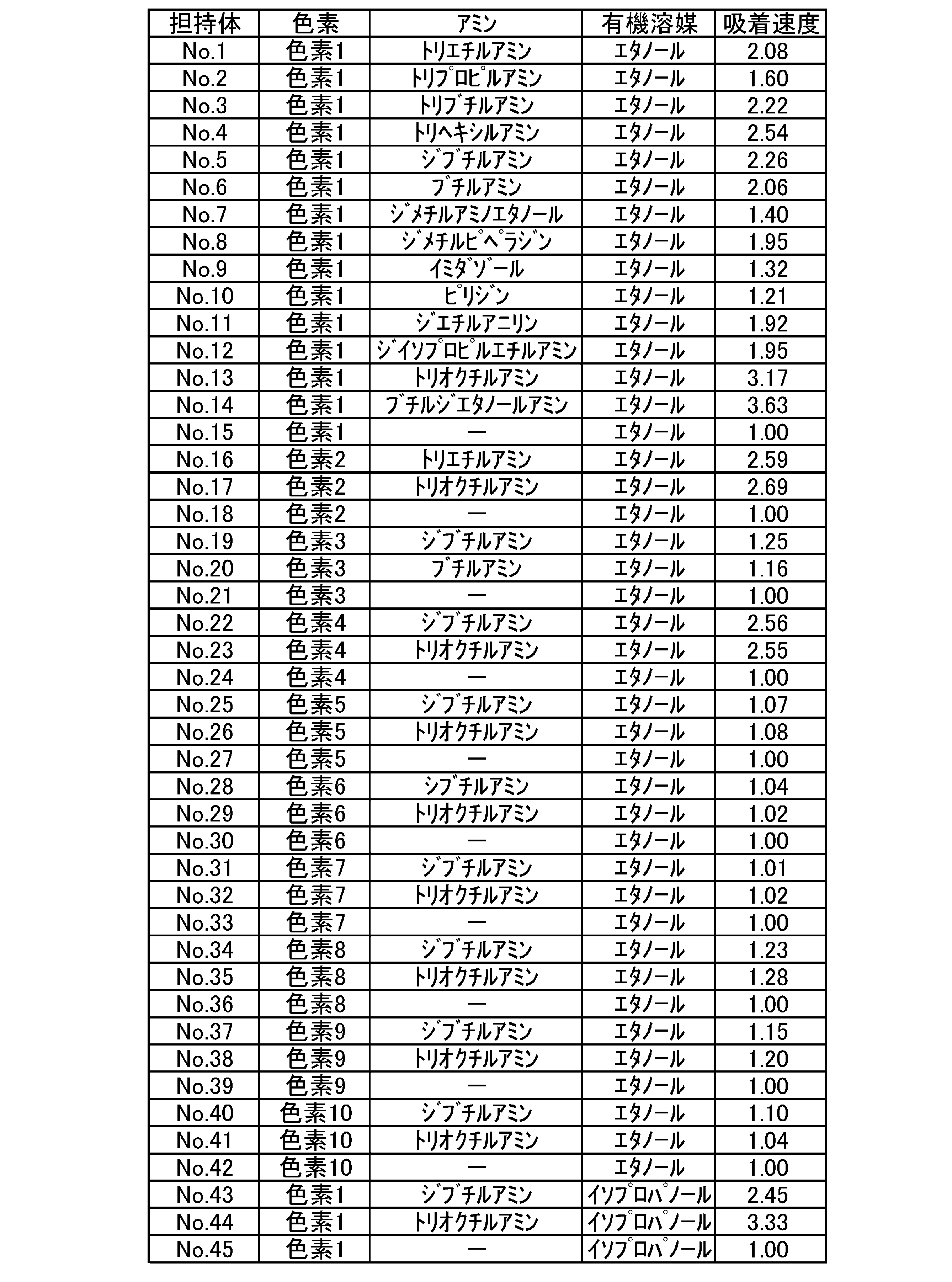
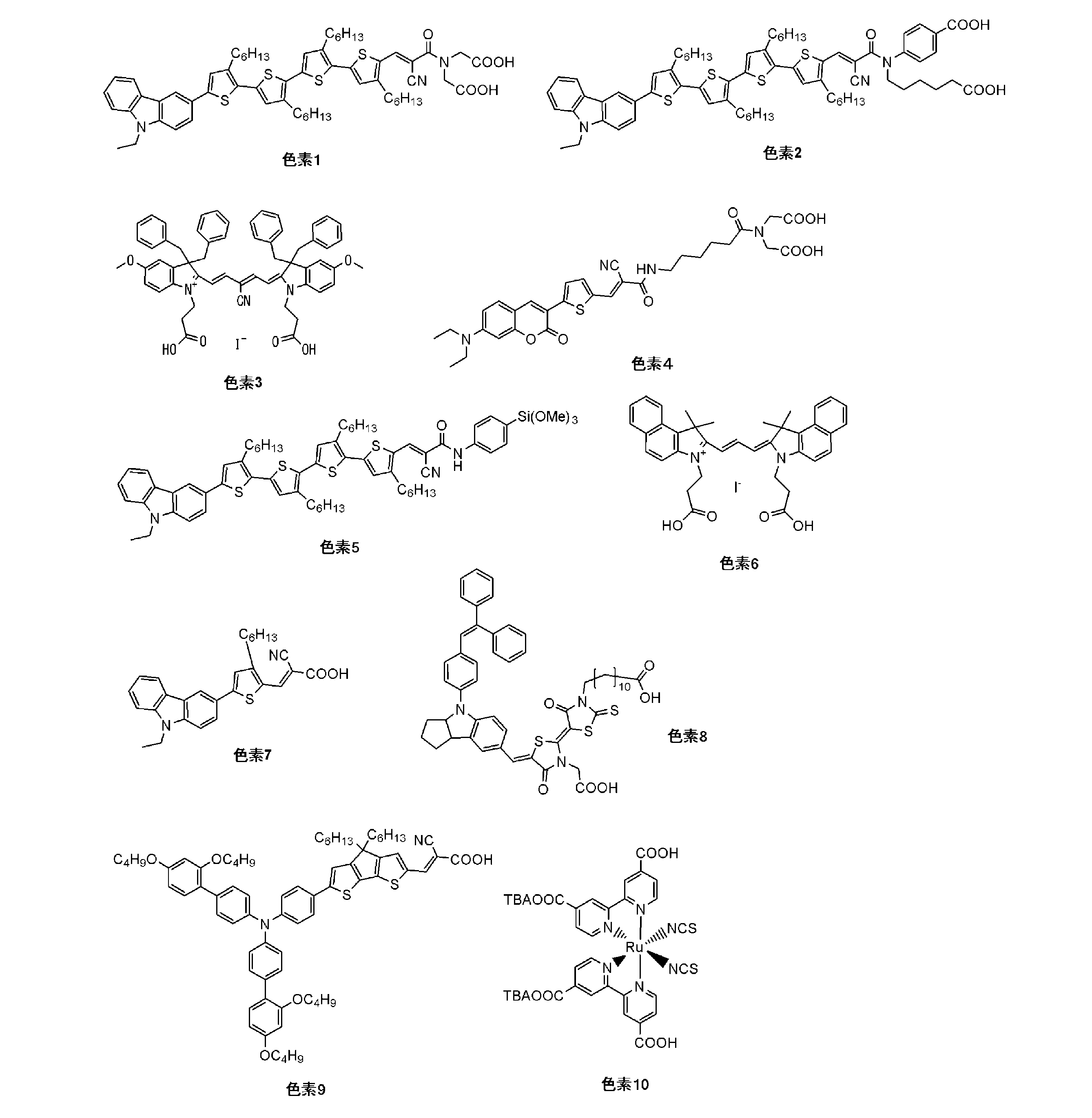
図1に示す光電変換素子を作製した。具体的には、作製した作用電極10と、導電性基板21としてITO電極(西野田電工(株)製)上に黒鉛微粒子(導電層22)をコーティングして作製した対向電極20とを、スペーサー(63μm)を介して対向させ、それらの間に電解質含有層30を配し、これらをクリップで固定し、電解質含有層30に電解液(アセトニトリルに対して、ヨウ素(0.05mM)、ヨウ化リチウム(0.5mM)を、それぞれ所定の濃度になるように混合したもの)を浸透させ、光電変換素子を作製した。セル上部を開口部1cmのマスクで覆い、AM-1.5G、100mW/cm2のソーラーシミュレーターで光電変換効率η(%)を測定した。
光電変換素子の測定値について、アミンを用いない場合の光電変換効率を1としたときの相対値を表2に示す。数値が大きいほど担持時にアミンを加えた効果が高く、光電変換効率に優れることを表す。

Claims (6)
- 有機溶媒中で担体に化合物を担持する方法であって、該有機溶媒がアミンを含有することを特徴とする担持方法。
- 前記有機溶媒が、水酸基を有する有機溶媒であることを特徴とする請求項1に記載の担持方法。
- 前記化合物が、カルボキシル基、スルホン酸基、リン酸基、ホスホン酸基又はアルコキシシリル基から選ばれる基を少なくとも一つ有する化合物であることを特徴とする請求項1又は2に記載の担持方法。
- 前記担体が、金属酸化物であることを特徴とする請求項1~3のいずれか一項に記載の担持方法。
- 請求項1~4のいずれか一項に記載の担持方法により得られる担持体。
- 請求項5に記載の担持体を有する電極を備えた光電変換素子。
Priority Applications (5)
| Application Number | Priority Date | Filing Date | Title |
|---|---|---|---|
| US15/304,883 US20170140879A1 (en) | 2014-05-20 | 2015-05-12 | Loading method, loaded body and photoelectric conversion element |
| JP2016521050A JPWO2015178257A1 (ja) | 2014-05-20 | 2015-05-12 | 担持方法、担持体及び光電変換素子 |
| KR1020167029906A KR20170008207A (ko) | 2014-05-20 | 2015-05-12 | 담지 방법, 담지체 및 광전 변환 소자 |
| EP15796248.1A EP3147332A4 (en) | 2014-05-20 | 2015-05-12 | Loading method, loaded body and photoelectric conversion element |
| CN201580023110.2A CN106459605A (zh) | 2014-05-20 | 2015-05-12 | 担载方法、担载体以及光电转换元件 |
Applications Claiming Priority (2)
| Application Number | Priority Date | Filing Date | Title |
|---|---|---|---|
| JP2014-104632 | 2014-05-20 | ||
| JP2014104632 | 2014-05-20 |
Publications (1)
| Publication Number | Publication Date |
|---|---|
| WO2015178257A1 true WO2015178257A1 (ja) | 2015-11-26 |
Family
ID=54553930
Family Applications (1)
| Application Number | Title | Priority Date | Filing Date |
|---|---|---|---|
| PCT/JP2015/063677 Ceased WO2015178257A1 (ja) | 2014-05-20 | 2015-05-12 | 担持方法、担持体及び光電変換素子 |
Country Status (7)
| Country | Link |
|---|---|
| US (1) | US20170140879A1 (ja) |
| EP (1) | EP3147332A4 (ja) |
| JP (1) | JPWO2015178257A1 (ja) |
| KR (1) | KR20170008207A (ja) |
| CN (1) | CN106459605A (ja) |
| TW (1) | TW201547038A (ja) |
| WO (1) | WO2015178257A1 (ja) |
Cited By (1)
| Publication number | Priority date | Publication date | Assignee | Title |
|---|---|---|---|---|
| JP2016051757A (ja) * | 2014-08-29 | 2016-04-11 | 積水化学工業株式会社 | 増感色素染色法 |
Families Citing this family (2)
| Publication number | Priority date | Publication date | Assignee | Title |
|---|---|---|---|---|
| CN110064438B (zh) * | 2019-04-26 | 2020-06-02 | 山东大学 | 一种有机膦酸修饰的NiO复合光催化剂及其制备方法和应用 |
| CN116715976B (zh) * | 2023-05-18 | 2024-08-06 | 大连理工大学 | 一类含手性碳的五甲川菁染料及其制备方法和应用 |
Citations (5)
| Publication number | Priority date | Publication date | Assignee | Title |
|---|---|---|---|---|
| JPS62288632A (ja) * | 1986-06-06 | 1987-12-15 | Nippon Paint Co Ltd | 着色架橋微小樹脂粒子 |
| JP2010009830A (ja) * | 2008-06-25 | 2010-01-14 | Konica Minolta Business Technologies Inc | 光電変換素子及びその製造方法、太陽電池 |
| WO2011145551A1 (ja) * | 2010-05-17 | 2011-11-24 | 日本化薬株式会社 | 熱硬化型光電変換素子用シール剤を用いた光電変換素子 |
| JP2012501831A (ja) * | 2008-09-05 | 2012-01-26 | アルストム テクノロジー リミテッド | 新規の固体物質及びガスストリームからのco2の除去法 |
| JP2013182771A (ja) * | 2012-03-01 | 2013-09-12 | Konica Minolta Inc | 色素増感型光電変換素子およびその製造方法、ならびに太陽電池 |
Family Cites Families (5)
| Publication number | Priority date | Publication date | Assignee | Title |
|---|---|---|---|---|
| JP4638972B2 (ja) * | 2000-03-13 | 2011-02-23 | 富士フイルム株式会社 | 光電極の作成方法、光電極、光電変換素子および光電池 |
| JP5280853B2 (ja) * | 2006-11-07 | 2013-09-04 | Agcセイミケミカル株式会社 | 新規アミノ基含有芳香族化合物および該芳香族化合物を含有する光電変換用増感色素 |
| JP2012084250A (ja) | 2010-10-07 | 2012-04-26 | Konica Minolta Business Technologies Inc | 光電変換素子及び太陽電池 |
| JP5673477B2 (ja) * | 2011-10-06 | 2015-02-18 | コニカミノルタ株式会社 | 光電変換素子 |
| JP5925541B2 (ja) | 2012-03-16 | 2016-05-25 | 富士フイルム株式会社 | 光電変換素子用金属錯体色素、光電変換素子、色素増感太陽電池、色素増感太陽電池用色素吸着組成液、色素増感太陽電池用半導体電極および色素増感太陽電池の製造方法 |
-
2015
- 2015-05-12 KR KR1020167029906A patent/KR20170008207A/ko not_active Withdrawn
- 2015-05-12 US US15/304,883 patent/US20170140879A1/en not_active Abandoned
- 2015-05-12 EP EP15796248.1A patent/EP3147332A4/en not_active Withdrawn
- 2015-05-12 JP JP2016521050A patent/JPWO2015178257A1/ja active Pending
- 2015-05-12 CN CN201580023110.2A patent/CN106459605A/zh active Pending
- 2015-05-12 WO PCT/JP2015/063677 patent/WO2015178257A1/ja not_active Ceased
- 2015-05-19 TW TW104115929A patent/TW201547038A/zh unknown
Patent Citations (5)
| Publication number | Priority date | Publication date | Assignee | Title |
|---|---|---|---|---|
| JPS62288632A (ja) * | 1986-06-06 | 1987-12-15 | Nippon Paint Co Ltd | 着色架橋微小樹脂粒子 |
| JP2010009830A (ja) * | 2008-06-25 | 2010-01-14 | Konica Minolta Business Technologies Inc | 光電変換素子及びその製造方法、太陽電池 |
| JP2012501831A (ja) * | 2008-09-05 | 2012-01-26 | アルストム テクノロジー リミテッド | 新規の固体物質及びガスストリームからのco2の除去法 |
| WO2011145551A1 (ja) * | 2010-05-17 | 2011-11-24 | 日本化薬株式会社 | 熱硬化型光電変換素子用シール剤を用いた光電変換素子 |
| JP2013182771A (ja) * | 2012-03-01 | 2013-09-12 | Konica Minolta Inc | 色素増感型光電変換素子およびその製造方法、ならびに太陽電池 |
Non-Patent Citations (1)
| Title |
|---|
| See also references of EP3147332A4 * |
Cited By (1)
| Publication number | Priority date | Publication date | Assignee | Title |
|---|---|---|---|---|
| JP2016051757A (ja) * | 2014-08-29 | 2016-04-11 | 積水化学工業株式会社 | 増感色素染色法 |
Also Published As
| Publication number | Publication date |
|---|---|
| EP3147332A4 (en) | 2018-01-10 |
| EP3147332A1 (en) | 2017-03-29 |
| JPWO2015178257A1 (ja) | 2017-04-20 |
| KR20170008207A (ko) | 2017-01-23 |
| CN106459605A (zh) | 2017-02-22 |
| US20170140879A1 (en) | 2017-05-18 |
| TW201547038A (zh) | 2015-12-16 |
Similar Documents
| Publication | Publication Date | Title |
|---|---|---|
| EP1981047A2 (en) | Photoelectric conversion device | |
| JP6145407B2 (ja) | 新規化合物及びこの新規化合物を担持した担持体 | |
| EP2800199B1 (en) | Dye-sensitized solar cell | |
| WO2014103831A1 (ja) | 担持体及び光電変換素子 | |
| WO2015178257A1 (ja) | 担持方法、担持体及び光電変換素子 | |
| KR20130075772A (ko) | 광전 변환 소자 및 광전 변환 소자용 색소, 그리고 화합물 | |
| JP5606754B2 (ja) | 色素増感型太陽電池 | |
| JP6113713B2 (ja) | 新規化合物及びこの新規化合物を担持した担持体 | |
| JP5914462B2 (ja) | 新規化合物及び光電変換素子 | |
| CN105340037A (zh) | 色素敏化型太阳能电池 | |
| JP5412955B2 (ja) | 電極および光電変換素子 | |
| JP5482290B2 (ja) | 光電変換素子 | |
| JP2010056029A (ja) | 光電変換素子 | |
| CN105874550B (zh) | 担载体和光电转换元件 | |
| JP2016219653A (ja) | 担持体及び光電変換素子 | |
| JPWO2016108269A1 (ja) | 化合物、担持体及び光電変換素子 |
Legal Events
| Date | Code | Title | Description |
|---|---|---|---|
| 121 | Ep: the epo has been informed by wipo that ep was designated in this application |
Ref document number: 15796248 Country of ref document: EP Kind code of ref document: A1 |
|
| DPE1 | Request for preliminary examination filed after expiration of 19th month from priority date (pct application filed from 20040101) | ||
| ENP | Entry into the national phase |
Ref document number: 2016521050 Country of ref document: JP Kind code of ref document: A |
|
| WWE | Wipo information: entry into national phase |
Ref document number: 15304883 Country of ref document: US |
|
| ENP | Entry into the national phase |
Ref document number: 20167029906 Country of ref document: KR Kind code of ref document: A |
|
| REEP | Request for entry into the european phase |
Ref document number: 2015796248 Country of ref document: EP |
|
| WWE | Wipo information: entry into national phase |
Ref document number: 2015796248 Country of ref document: EP |
|
| NENP | Non-entry into the national phase |
Ref country code: DE |