WO2015194370A1 - 電流検出装置 - Google Patents
電流検出装置 Download PDFInfo
- Publication number
- WO2015194370A1 WO2015194370A1 PCT/JP2015/065966 JP2015065966W WO2015194370A1 WO 2015194370 A1 WO2015194370 A1 WO 2015194370A1 JP 2015065966 W JP2015065966 W JP 2015065966W WO 2015194370 A1 WO2015194370 A1 WO 2015194370A1
- Authority
- WO
- WIPO (PCT)
- Prior art keywords
- magnetic shield
- shield member
- current detection
- detection device
- conductor
- Prior art date
- Legal status (The legal status is an assumption and is not a legal conclusion. Google has not performed a legal analysis and makes no representation as to the accuracy of the status listed.)
- Ceased
Links
Images






Classifications
-
- G—PHYSICS
- G01—MEASURING; TESTING
- G01R—MEASURING ELECTRIC VARIABLES; MEASURING MAGNETIC VARIABLES
- G01R15/00—Details of measuring arrangements of the types provided for in groups G01R17/00 - G01R29/00, G01R33/00 - G01R33/26 or G01R35/00
- G01R15/14—Adaptations providing voltage or current isolation, e.g. for high-voltage or high-current networks
- G01R15/20—Adaptations providing voltage or current isolation, e.g. for high-voltage or high-current networks using galvano-magnetic devices, e.g. Hall-effect devices, i.e. measuring a magnetic field via the interaction between a current and a magnetic field, e.g. magneto resistive or Hall effect devices
- G01R15/202—Adaptations providing voltage or current isolation, e.g. for high-voltage or high-current networks using galvano-magnetic devices, e.g. Hall-effect devices, i.e. measuring a magnetic field via the interaction between a current and a magnetic field, e.g. magneto resistive or Hall effect devices using Hall-effect devices
-
- G—PHYSICS
- G01—MEASURING; TESTING
- G01R—MEASURING ELECTRIC VARIABLES; MEASURING MAGNETIC VARIABLES
- G01R15/00—Details of measuring arrangements of the types provided for in groups G01R17/00 - G01R29/00, G01R33/00 - G01R33/26 or G01R35/00
- G01R15/14—Adaptations providing voltage or current isolation, e.g. for high-voltage or high-current networks
- G01R15/20—Adaptations providing voltage or current isolation, e.g. for high-voltage or high-current networks using galvano-magnetic devices, e.g. Hall-effect devices, i.e. measuring a magnetic field via the interaction between a current and a magnetic field, e.g. magneto resistive or Hall effect devices
- G01R15/207—Constructional details independent of the type of device used
Definitions
- the present invention relates to a current detection device capable of measuring a current flowing through a conductor in a non-contact manner, and in particular, a current suitable for being used for detecting a large current in a power conversion device such as a HEV (hybrid vehicle) or EV (electric vehicle).
- a power conversion device such as a HEV (hybrid vehicle) or EV (electric vehicle).
- the present invention relates to a detection device.
- a current detection device using a U-shaped magnetic shield is known as a coreless current detection device in which a magnetic core is removed.
- a magnetic core is removed.
- the saturation magnetic flux of the magnetic shield decreases.
- the magnetic shield has a magnetic flux collecting function.
- the Hall element detects a magnetic flux
- a decrease in the saturation magnetic flux of the magnetic shield leads to a decrease in the maximum detectable current.
- the magnetic shield is composed of a plurality of shield materials.
- the conductor has a rectangular cross section that is vertically short and long to the left and right, and the magnetic shield is provided on two short side walls (side walls) disposed on the two short sides of the conductor and on the long side of the conductor.
- the magnetic shield has a cross-sectionally reduced portion such as a gap, a cut, or a through hole in the long side wall portion, thereby increasing the magnetic flux leaking to the outer surface side of the magnetic shield and decreasing the magnetic flux passing through the magnetic shield.
- the maximum detectable current is increased while suppressing a decrease in the saturation magnetic flux of the magnetic shield.
- a shield opening In the structure in which a gap or a through-hole (hereinafter referred to as a shield opening) is provided in the long side wall, external disturbance magnetic flux enters the inside of the magnetic shield from the shield opening, so that the reliability of the current sensor is improved. There is a risk of lowering.
- magnetic flux collects at the portion where the cross-sectional area changes inside the magnetic shield, resulting in a portion with a high magnetic flux density, which reduces the saturation magnetic flux inside the magnetic shield. There is a problem that the maximum current that can be detected decreases.
- An object of the present invention is to provide a current detection device that is not easily affected by disturbance magnetic flux and hardly causes a decrease in the maximum detectable current.
- the current detection device of the present invention includes a first magnetic field having a side wall portion covering one side of a conductor and a protruding portion protruding from the side wall portion toward the other side.
- a first magnetic shield comprising: a shield member; and a second magnetic shield member having a side wall portion covering the other side of the conductor and a protruding portion protruding from the side wall portion toward the one side side.
- the protruding portion of the member and the protruding portion of the second magnetic shield member form a gap while overlapping in the protruding direction of the protruding portion.
- 1 is a perspective view of a current detection device according to the present invention. It is a block diagram which shows the example which changed arrangement
- FIG. 1 is a configuration diagram of a current detection device according to the present embodiment.
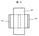
- FIG. 2 is a top view of the current detection device according to the present embodiment.
- FIG. 3 is a perspective view of the current detection device according to the present embodiment. 1 corresponds to the II ′ cross section of FIG.
- the vertical direction is defined based on FIG. 1 and is not related to the vertical direction in the mounted state of the current detection device.
- the current detection device 100 includes an L-shaped first magnetic shield member 111 and a second magnetic shield part 112 that are magnetic bodies, a Hall element 113 provided as a current sensor, and a conductor 121.
- the first magnetic shield member 111, the second magnetic shield portion 112, and the hall element 113 are fixed to a printed circuit board (substrate member) 115.
- the printed board 115 is made of an insulating material and is nonmagnetic.
- the first magnetic shield member 111, the second magnetic shield part 112, the conductor 121, and the Hall element 113 are covered with a resin 116 together with the printed board 115.
- the Hall element 113 is embedded in the resin 116.
- the Hall element 113 may be disposed outside the resin 116 in a substrate-less configuration as shown in FIG.
- the hall element 113 is fixed to the printed circuit board 115 by fixing a plurality of terminals 113 a to the printed circuit board 115.
- the plurality of terminals 113a are electrically connected to terminals 117 exposed from the resin.
- the plurality of terminals 113a of the Hall element 113 may be exposed from the resin 116 and used as a substitute for the terminal 117.
- the current detection target conductor 121 has a rectangular cross section that is short in the vertical direction and long in the left and right directions, and the inner surface side space of the magnetic shields 111 and 112 constituted by the first magnetic shield member 111 and the second magnetic shield member 112. It is disposed through. The current flows along the longitudinal direction (extending direction) of the conductor 121.
- the first magnetic shield member 111 and the second magnetic shield member 112 are arranged to face each other with the conductor 121 interposed therebetween.
- the first magnetic shield member 111 and the second magnetic shield member 112 are made of a magnetic material.
- Each of the first magnetic shield member 111 and the second magnetic shield member 112 is L-shaped.
- the first magnetic shield member 111 extends in a direction crossing the side wall portion 111a from the lower end portion of the side wall portion 111a toward the second magnetic shield member 112 side, covering the side of the conductor 121.
- a bottom portion 111b The second magnetic shield member 112 extends in a direction crossing the side wall portion 112a from the lower end portion of the side wall portion 112a toward the first magnetic shield member 111 side, covering the side of the conductor 121.
- a bottom 112b is
- the bottom portion 111b of the first magnetic shield member 111 and the bottom portion 112b of the second magnetic shield member 112 are arranged offset in the vertical direction so as to form a vertical gap 131 below the conductor 121. . Further, the bottom 111b of the first magnetic shield member 111 and the bottom 112b of the second magnetic shield member 112 are disposed so as to overlap in the extending direction.
- the straight line 141 is a line segment perpendicular to the board surface of the printed board 115 (the mounting surfaces of the first magnetic shield member 111, the second magnetic shield member 112, and the Hall element 113), and the side wall part 111a and the side wall part 112a. Is equidistant from. 1 is a cross-sectional view, and when considering the depth direction of FIG. 1, the straight line 141 may be considered as a plane extending in the depth direction of FIG.
- the side wall part 111a and the side wall part 112a have a plane parallel to this plane (hereinafter referred to as a side wall surface).
- the first magnetic shield member 111 is disposed on one side of the conductor 121
- the second magnetic shield member 112 is disposed on the other side of the conductor 121.
- the side wall portion 111 a of the first magnetic shield member 111 and the side wall portion 112 a of the second magnetic shield member 112 face each other with the conductor 121 interposed therebetween.
- the bottom 111 b of the first magnetic shield member 111 and the bottom 112 b of the second magnetic shield member 112 cover the lower part of the conductor 121.
- the first magnetic shield member 111 and the second magnetic shield member 112 collect magnetic flux generated according to the right-handed screw law around the conductor 121, and the first magnetic shield member 111 and the second magnetic shield member 112 are arranged inside the first magnetic shield member 111 and the second magnetic shield member 112. Form magnetic flux lines. This magnetic flux line leaks from one of the first magnetic shield member 111 and the second magnetic shield member 112 at the gap 131 and moves to the other magnetic shield member.
- the Hall element 113 as a current sensor is disposed on a straight line 141 connecting the conductor 121 and the gap 131 and is fixed to the printed board 115.
- the main part of the magnetic flux line extending between the first magnetic shield 111 and the second magnetic shield member 112 on the printed board 115 side extends substantially along the printed board 115. For this reason, most of the extended magnetic flux passes through the Hall element 113.
- the Hall element 113 can detect a minute magnetic flux generated by the current flowing through the conductor 121 by the magnetic flux collecting function of the magnetic shields 111 and 112, and the magnetic detection sensitivity is increased.
- the Hall element 113 outputs a voltage proportional to the magnetic flux density by applying a predetermined current.
- the configuration using the printed circuit board 115 is used, but a configuration without a printed circuit board 115 may be used.
- the first magnetic shield 111, the second magnetic shield member 112, the conductor 121, and the hall element 113 are fixed by the resin mold 116.
- Each structure can be easily fixed at a predetermined position by the resin mold 116.
- the current value of the conductor 121 is approximately linear and proportional.
- the current value of the conductor 121 increases and the magnetic flux density inside the magnetic shields 111 and 112 reaches the saturation magnetic flux density of the magnetic shield, it extends between the first magnetic shield 111 and the second magnetic shield member 112.
- the linear proportional relationship existing between the magnetic flux density of the existing magnetic flux lines and the current value of the conductor 121 is lost. For this reason, it is impossible to accurately measure the current value of the conductor 121 by the Hall element 113.
- the current value of the conductor 121 that can be measured by the Hall element 113 is determined by the magnitude of the saturation magnetic flux density in the magnetic shields 111 and 112.
- the gap 131 is formed in the bottom portion (the bottom portion 111b and the bottom portion 112b) constituted by the first magnetic shield member 111 and the second magnetic shield member 112.
- the gap 131 divides the magnetic path formed at the bottom of the magnetic shield and moderately reduces the magnetic flux density inside the magnetic shield. Further, the gap 131 has a function of reducing the magnetic flux density of the magnetic flux lines extending between the magnetic shields.
- the magnetic flux lines existing in the current detection device 100 are between the magnetic shields 111 and 112. Extends substantially perpendicular to the shield side surface and penetrates the Hall element 113. As a result, the Hall element 113 senses a magnetic flux that is substantially proportional to the current of the conductor 121, and outputs a voltage proportional to the magnetic flux.
- the conductor 121 is in the vicinity of the bottom of the first magnetic shield member 111 and penetrates the inner space formed by the first magnetic shield member 111 and the second magnetic shield member 112. Yes.
- the first magnetic shield member 111 and the conductor 1 There is a gap between 21. This gap can be reduced or eliminated if there is no problem with magnetic saturation inside the magnetic shields 111 and 112. That is, an insulator may be disposed between the first magnetic shield member 111 and the conductor 121, and the first magnetic shield member 111 may be fixed to the bottom surface of the conductor 121 via the insulator.
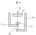
- FIG. 4 is a configuration diagram showing an example in which the arrangement of the Hall elements 113 is changed.
- the printed circuit board 115 and the resin 116 described in FIG. 1 are omitted, but the printed circuit board 115 and the resin 116 are configured in the same manner as in FIG.
- the Hall element 113 is a space between the conductor 121 and the bottom portions (the bottom portion 111 b and the bottom portion 112 b) of the magnetic shields 111 and 112 configured by the first magnetic shield member 111 and the second magnetic shield member 112. Is arranged. Such an arrangement may be adopted.
- FIG. 5 is a configuration diagram showing a modified example in which the first magnetic shield member 111 and the second magnetic shield member 112 have the same shape.
- the length of the side wall portion 111a of the first magnetic shield member 111 is equal to the length of the side wall portion 112a of the second magnetic shield member 112. And the upper end surface of the side wall part 111a of the 1st magnetic shield member 111 and the upper end surface of the side wall part 112a of the 2nd magnetic shield member 111 are shifted and fixed.
- Such a configuration can be easily realized by a structure in which the first magnetic shield member 111 and the second magnetic shield member 112 are fixed by the resin mold 116 without using the printed circuit board 115. It is also possible to use the printed circuit board 115 by devising, for example, providing a stepped part at the attachment part to the printed circuit board 115.
- the first magnetic shield member 111 and the second magnetic shield member 112 can be configured using the same member, so that productivity is improved.
- FIG. 6 is a diagram illustrating a configuration in which the current detection device 100 according to the present embodiment is mounted on the power conversion device 411.
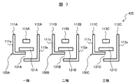
- FIG. 7 is a schematic diagram illustrating a three-phase current detection device configured by the current detection device 100 according to the present embodiment.
- the current detection device shown in FIG. 7 parts having the same structure as those of the current detection device of FIG. Description of parts having the same structure is omitted, and only differences are described.
- a one-phase current detection device and a two-phase current detection device will be described. The interaction between adjacent current detection devices exists not only between one phase and two phases, but also between two phases and three phases and between three phases and one phase.
- the power conversion device 411 includes a microcomputer 421, a drive circuit 422, a power module 423, a capacitor 424, a current detection device 425, a conductor 426 (121), and a terminal 427.
- the power conversion device 411 is used for operating the motor 428 and the like.
- the current detection device 425 is disposed on a conductor 426 including a bus bar between the power module 423 and the terminal 427.
- the current detection device 425 measures the current value output from the power module 423 and feeds back the detected current value to the microcomputer 421.
- similar current detection devices 100A, 100B, and 100C are arranged in the left-right direction.
- three current detection devices 100 shown in FIG. 1 are arranged to constitute a three-phase current detection device 425.
- Each of the current detection devices 100A, 100B, and 100C includes a first magnetic shield member 111A, 111B, and 111C, a second magnetic shield member 112A, 112B, and 112C, conductors 121A, 121B, and 121C, and a hall element 113A, 113B and 113C are provided.
- the length of the side wall 111a is different from the length of the side wall 111b.
- the three-phase current detection device 425 using the current detection devices 100 side by side has the length of the two-phase first magnetic shield 111B adjacent to the one-phase current detection device (the length of the side wall), two Length of one-phase second magnetic shield 112A adjacent to the phase current detection device ( The length of the side wall).
- the long side wall portion 112a of the one-phase current detection device 100A and the short side wall portion 111a of the two-phase current detection device 100B are adjacent to each other. To do. Further, between the two-phase current detection device 100B and the three-phase current detection device 100C, the long side wall portion 112a of the two-phase current detection device 100B and the short side wall portion 111a of the three-phase current detection device 100C are adjacent to each other. To do.
- the current detection device 100 is not concerned about the arrangement order of the long side wall portions 112a and the short side wall portions 111a. May be arranged.
- FIG. 8 is a front view of the three-phase current detection device 425 according to this configuration example.
- the first magnetic shield members 111A, 111B, and 111C, the second magnetic shield members 112A, 112B, and 112C, and the conductor 121 are fixed by a resin mold 116 in advance.
- the hall elements 113A, 113B, and 113C are arranged outside the resin mold 116, so that the assembly becomes easy. Adjustment is made by retrofitting the Hall elements 113A, 113B, and 113C to an assembly including the first magnetic shield members 111A, 111B, and 111C, the second magnetic shield members 112A, 112B, and 112C, the conductor 121, and the resin mold 116.
- all the parts constituting the three-phase current detection device 426 including the Hall elements 113A, 113B, and 113C may be integrated by the resin mold 116.
- FIG. 8 The configuration of FIG. 8 is applied to the current detection device 100 of FIGS. 1 and 5, and the first magnetic shield member 111, the second magnetic shield member 112, and the conductor 121 are fixed with a resin mold 116, and the Hall element 113. May be arranged outside the resin mold 116.
- FIG. 9 is a top view showing an example in which the three-phase current detection device according to the present invention is applied to a power conversion device used for HEV, EV, or the like.
- the three-phase current detection device 425 is used for individually measuring the currents of the U phase, the V phase, and the W phase of a power conversion device used for, for example, HEV and EV.
- a current detection device 100A is provided in the U phase.
- a current detection device 100B is provided in the V phase.
- a current detection device 100C is provided in the W phase.
- a current flows through each conductor 121 in the longitudinal direction of the conductor 121.
- Bolt holes 161A, 161B, 161C are provided in the longitudinal ends of the conductors 121A, 121B, 121C, and are fixed to the output terminal 427 (see FIG. 6) using mounting bolts.
- One end portion in the longitudinal direction is fixed by welding to an output terminal of the power module 423 (see FIG. 6), and each phase current input portion (wiring) is connected to the conductors 121, 121B, and 121C.
- Each of the conductors 121A, 121B, and 121C can be constituted by an output terminal of the power module 423. In this case, it is not necessary to fix the conductors 121A, 121B, and 121C by welding. Further, the power module 423 and the three-phase current detection device 425 are integrated. Alternatively, the conductors 121A, 121B, and 121C and the first magnetic shield member 111 and a part of the second magnetic shield member 112 are exposed from the resin mold 116, whereby the conductor 121A configured by the output terminal of the power module 423 is used. , 121B, 121C can be assembled with a three-phase current detection device 425 configured separately. In this case, the three-phase current detection device 425 does not have the conductors 121A, 121B, and 121C. Such a configuration in which the conductor 121 is separated is also applicable to the configurations described with reference to FIGS.
- the only gap 131 (131A, 131B, 131C) is generally the conductor 121 (121A). , 121B, 121C) is formed on a straight line 141 (see FIG. 1) passing through the center of the cross section. Therefore, since the magnetic flux leaking from the gap 131 leaks toward the lower side of the current detection device 100 (100A, 100B, 100C), it is possible to suppress entry into the adjacent current detection device.
- the magnetic flux lines generated between the first magnetic shield member 111 and the second magnetic shield member 112 are magnetic shields 111 and 112 except for the vicinity of the magnetic shields 111 and 112.
- the space extends along the substrate.
- the Hall element 113 is generally disposed on the straight line 141 that connects the gap 131 and the conductor 121.
- the Hall element 113 does not have to be arranged on the straight line 141 (the center of the conductor 121), and may be arranged with respect to the straight line 141.
- the arrangement of the Hall elements 113 is not limited.
- FIG. 10 is a diagram showing a configuration in which the current detection devices 100A, 100B, and 100C are vertically arranged.
- the current detection devices 100A, 100B, and 100C are arranged adjacently (laterally arranged) so that the side wall portions of the magnetic shield members face each other.
- it may be arranged (vertically arranged) so that the bottoms of the magnetic shield members face the same direction.
- FIG. 11 is a diagram illustrating a state where the conductor 171 is disposed at a position facing the bottom of the current detection device 100.
- the first magnetic shield member 111 and the second magnetic shield member 112 overlap at the bottom of the current detection device 100.
- FIG. 12 is a diagram illustrating a modified example in which the configuration of the gap 131 is changed.
- the protruding length of the bottom 111b is equal to the protruding length of the bottom 112b. That is, for example, as shown in FIG. 1, the gap 131 is substantially located on the straight line 141. However, as shown in FIG. 12, the protruding length of the bottom 111b may be different from the protruding length of the bottom 112b. In this case, the gap 131 is provided eccentrically with respect to the straight line 141 (the cross-sectional center of the conductor 121).
- the protruding length of the bottom 111b is different from the protruding length of the bottom 112b, the protruding length of the bottom 111b arranged on the inner side (the conductor 121 or the Hall element 113 side) is larger than the protruding length of the bottom 112b arranged on the outer side. It is preferable to lengthen the length. As a result, a structure in which the conductor 121 or the Hall element 113 is not easily seen from the gap 131 can be realized.
- FIG. 13 shows the characteristics (analysis result) of the output voltage with respect to the current value when the current detection device 100 according to the present embodiment (FIG. 1) is used and when the current detection device shown in FIG. 14 is used.
- FIG. FIG. 14 is a diagram illustrating a configuration of a current detection device configured with a U-shaped shield.
- the presence of the gap 131 causes the magnetic flux to leak outside the first magnetic shield member 111 and the second magnetic shield member 112 through the gap 131, thereby The magnetic flux density of the magnetic flux lines existing in the space surrounded by the shield member 111 and the second magnetic shield member 112 is lowered. As a result, the sensor output corresponding to the current value of the conductor 121 decreases, and the measurable current value increases.
- the conductors 121, 121A, 121B, and 121C have a rectangular shape in which a transverse section (a section perpendicular to the longitudinal direction) has a long side and a short side.
- the side wall portion 111a of the first magnetic shield member 111 and the side wall portion 112a of the second magnetic shield member 112 constitute a short side wall portion disposed on the short side of the conductors 121, 121A, 121B, and 121C.
- the bottom portion 111b of the first magnetic shield member 111 and the bottom portion 112b of the second magnetic shield member 112 constitute a long side wall portion disposed on the long side of the conductors 121, 121A, 121B, and 121C.
- the side wall portion 111a of the first magnetic shield member 111 and the side wall portion 112a of the second magnetic shield member 112 are disposed on both sides (both sides) of the conductors 121, 121A, 121B, 121C, and the conductors 121, 121A, Both side wall portions or opposed side wall portions facing each other across 121B and 121C are formed.
- the bottom portion 111b of the first magnetic shield member 111 and the bottom portion 112b of the second magnetic shield member 112 constitute one side wall portion disposed on one side (one side) of the conductors 121, 121A, 121B, and 121C. .
- the one side wall portions 111b and 112b are formed so as to project vertically from the one side wall portions 111a and 112a toward the other side wall portions 112a and 111a, or to be bent vertically. It constitutes a bend.
- the side wall portions 112a and 111a and the one side wall portions 111b and 112b are each formed in a flat plate shape.
- the side wall portions 112a and the side wall portions 111a are parallel to each other.
- the one side wall part 111b and the one side wall part 112b are parallel.
- FIG. 15 is an explanatory diagram of an overlap structure.
- the Hall element 113 and the conductor 121 are omitted.
- the side wall portions 111a and 112a extend in the extending direction (the direction indicated by the arrow E1).
- a gap 131 is provided, and an overlap amount of 0 mm or more is provided.
- FIG. 15 shows a case where the overlap amount is 0 mm. That is, the front end surface 111b-tS of the one side wall portion 111b and the front end surface 112b-tS of the one side wall portion 112b are located on the virtual plane S2.
- the virtual plane S2 is a plane parallel to the virtual plane S1.
- the virtual plane S1 is a plane virtually imaginary at an equal distance L from the side wall portions 111a and the side wall portions 112a.
- the virtual plane S1 is a plane including the straight line 141 in FIG.
- the virtual plane S2 including the tip surface 111b-tS of the one side wall portion 111b and the tip surface 112b-tS of the one side wall portion 112b is offset from the virtual plane S1 by a distance l.
- the virtual plane S2 may coincide with the virtual plane S1.
- the overlap amount is 0 mm, but the overlap amount is preferably larger than 0 mm. That is, it is preferable that the one side wall portion 111 b and the one side wall portion 112 b are reliably overlapped so that the disturbance magnetic flux does not reach the Hall element 113.
- the tip end portion 111b-t of the one side wall portion 111b and the tip end portion 112b-t of the one side wall portion 112b are They coincide on the virtual plane S3, and no gap is generated between the tip end portion 111b-t of the one side wall portion 111b and the tip end portion 112b-t of the one side wall portion 112b.
- the overlap structure in this embodiment is intended for a configuration in which no gap is generated between the tip end portion 111b-t and the tip end portion 112b-t when projected onto the virtual plane S3, and the overlap amount is 0 mm. Cases are also included.
- the tip end portion 111b-t of the one side wall portion (projecting portion) 111b and the tip end portion 112b-t of the one side wall portion (projecting portion) 112b are perpendicular to the protruding direction E2 of the one side wall portion 111b, 112b.
- a gap 131 is provided so as to be separated in a direction perpendicular to the extending direction of the conductor 121. That is, the front end portion 111b-t and the front end portion 112b-t are offset in a direction perpendicular to the protruding direction E2 of the one side wall portions 111b and 112b and perpendicular to the extending direction of the conductor 121. Further, the tip end portion 111b-t and the tip end portion 112b-t overlap in the protruding direction E2 of the one side wall portions 111b, 112b.
- this invention is not limited to each above-mentioned Example, Various modifications are included.
- the above-described embodiments have been described in detail for easy understanding of the present invention, and are not necessarily limited to those having all the configurations.
- a part of the configuration of one embodiment or modification can be replaced with the configuration of another embodiment or modification, and the configuration of another embodiment or modification can be replaced with the configuration of one embodiment or modification.
Landscapes
- Physics & Mathematics (AREA)
- General Physics & Mathematics (AREA)
- Measuring Instrument Details And Bridges, And Automatic Balancing Devices (AREA)
Abstract
Description
イブリッド自動車)やEV(電気自動車)等の電力変換装置で大電流検出用として用いられるのに好適な電流検出装置に関する。
れている。導体は上下に短く左右に長い矩形状横断面を有し、磁気シールドは導体の2つの短辺側に配設される2つの短辺側側壁部(側壁部)と、導体の長辺側に配設される1つ
の長辺側側壁部(底壁部)とを有する。磁気シールドは、長辺側側壁部に隙間、切れ込み又は貫通孔等の断面縮小部を有することで、磁気シールドの外面側へ漏れ出る磁束を増大させ、磁気シールドを通す磁束を減少させる。これにより、磁気シールドの飽和磁束の減少を抑制しつつ、検出可能な最大電流を増大させている。
、本実施例に係る電流検出装置の構成図である。図2は、本実施例に係る電流検出装置の上面図である。図3は、本実施例に係る電流検出装置の斜視図である。なお、図1は図3のI-I’断面に相当する。以下の説明において、上下方向は図1に基づいて定義され、電流検出装置の実装状態における上下方向とは関係がない。
本実施例によれば、第一の磁気シールド部材111及び第二の磁気シールド部材112により構成される底部(底部111b及び底部112b)に、隙間131が形成される。隙間131は、磁気シールド底部に形成される磁路を分断し、磁気シールド内部における磁束密度を適度に低下させる。また、隙間131には、磁気シールド間に延在する磁束線の磁束密度も低下させる機能がある。
、磁気シールド111及び112間をシールド側面に対してほぼ垂直に延在して、ホール素子113を貫通する。この結果、ホール素子113は導体121の電流に対して、ほぼ比例する磁束を感知し、この磁束に比例した電圧を出力する。
21との間に隙間が存在する。この隙間は、磁気シールド111及び112内部における磁気飽和が問題ないのであれば、小さくするか、或いは無くすことができる。すなわち、第一の磁気シールド部材111と導体121との間に絶縁体を配置し、導体121の底面に絶縁体を介して第一の磁気シールド部材111を固定しても良い。
。
、本実施例に係る電流検出装置100を電力変換装置411に搭載した構成を示す図である。図7は、本実施例に係る電流検出装置100で構成した三相電流検出装置を示す模式図である。図7に示す電流検出装置では、図1の電流検出装置と同一の構造である部分については、同一の符号を付けている。同一の構造である部分については説明を省略し、相違点のみ説明する。なお、以下の説明では、一相の電流検出装置及び二相の電流検出装置について説明する。隣接する電流検出装置同士における相互作用は、一相と二相との間だけでなく、二相と三相との間及び三相と一相との間にも同様に存在する。
図7に示すように、この三相電流検出装置425では、左右方向に同様な電流検出装置100A,100B,100Cを配置している。具体的には、図1に示す電流検出装置100を3個(100A,100B,100C)並べて、三相電流検出装置425を構成している。各電流検出装置100A,100B,100Cには、第一の磁気シールド部材111A,111B,111Cと、第二の磁気シールド部材112A,112B,112Cと、導体121A,121B,121Cと、ホール素子113A,113B,113Cとが設けられている。
側壁部の長さ)とが異なる。
。ホール素子113A,113B,113Cを第一の磁気シールド部材111A,111B,111C、第二の磁気シールド部材112A,112B,112C、導体121及び樹脂モールド116からなる組体に後付けとすることで、調整後にホール素子の不具合・損傷等が生じた場合、導体426を含めた電流検出装置100A,100B,100Cを破棄することなく、ホール素子113A,113B,113Cのみの付け替えが可能である。これにより、製造上のコストを削減することができ、有利である。
、ホール素子113を樹脂モールド116の外側に配置してもよい。
、W相の各相の電流を個別に測定するために用いられる。U相には電流検出装置100Aが設けられる。V相には電流検出装置100Bが設けられる。W相には電流検出装置100Cが設けられる。各導体121には導体121の長手方向に向かって電流が流れる。導体121A,121B,121Cには長手方向端部にボルト孔161A,161B,161Cが設けられ、取り付けボルトを用いて、出力端子427(図6参照)に固定される。一方の長手方向端部はパワーモジュール423(図6参照)の出力端子と溶接されることで固定され、導体121,121B,121Cに各相電流の入力部(配線)が接続される
。
,121B,121C)の断面中心を通る直線141(図1参照)上に形成される。したがって、隙間131から漏れる磁束は、電流検出装置100(100A,100B,100C)の下側に向かって漏れ出るので、隣接する電流検出装置への進入を抑制できる。
、磁気シールド111及び112間を基板に沿うよう延在する。このため、磁気シールド111及び112近傍を除いて、磁束線における磁束密度は、磁気シールド側面に対して垂直方向では変化量が小さくなる。上述した構成では、ホール素子113は、概ね、隙間131と導体121とを結ぶ直線141上に配置されている。しかし、上述した理由から
、ホール素子113は、直線141上(導体121の中心)に配置する必要がなく、直線141に対してずらした配置としても良い。本実施例は、ホール素子113の配置について限定するものではない。
。しかし、図12に示すように、底部111bの突出し長さと底部112bの突出し長さとが異なるようにしてもよい。この場合、隙間131は直線141(導体121の断面中心)に対して、偏奇して設けられる。なお、底部111bの突出し長さと底部112bの突出し長さとが異なる場合、内側(導体121或いはホール素子113側)に配置される底部111bの突出し長さを外側に配置される底部112bの突出し長さよりも長くすることが好ましい。これにより、隙間131から導体121或いはホール素子113を見通しにくい構造を実現することができる。
。第一の磁気シールド部材111の底部111b及び第二の磁気シールド部材112の底部112bは、導体121,121A,121B,121Cの長辺側に配設される長辺側側壁部を構成する。
。例えば、上記した実施例は本発明を分かりやすく説明するために詳細に説明したものであり、必ずしも全ての構成を備えるものに限定されるものではない。また、ある実施例又は変更例の構成の一部を他の実施例又は変更例の構成に置き換えることが可能であり、また、ある実施例又は変更例の構成に他の実施例又は変更例の構成を加えることも可能である。また、各実施例又は変更例の構成の一部について、他の構成の追加・削除・置換をすることが可能である。
,111C…第一の磁気シールド部材、111a…第一の磁気シールド部材111の側壁部、111b…第一の磁気シールド部材111の底部、111b-t…低部111bの先端部、111b-tS…低部111bの先端面、112,112A,112B,112C…第二の磁気シールド部、112a…第二の磁気シールド部材112の側壁部、112b…第二の磁気シールド部材112の底部、112b-t…低部112bの先端部、112b-tS…低部112bの先端面、113,113A,113B,113C…ホール素子
、113a…ホール素子113の端子、115…プリント基板(基板部材)、116…樹
脂(樹脂モールド)、117…プリント基板の端子、121,121A,121B,12
1C…導体、131,131A,131B,131C…隙間、161A,161B,161C…ボルト孔、171…外乱となる導体、411…電力変換装置、421…マイコン、422…ドライブ回路、423…パワーモジュール、424…コンデンサ、425…電流検出装置、426…導体、427…端子、428…モータ。
Claims (6)
- 電流センサと、前記電流センサの周囲に配置され内側に導体が配設される領域を有する磁気シールドとを備えた電流検出装置において、
前記磁気シールドは、導体を挟んで配置される第一の磁気シールド部材と第二の磁気シールド部材とを備え、
前記第一の磁気シールド部材は、導体を挟んで前記第二の磁気シールド部材と対向する対向側壁部と、前記対向側壁部から前記第二の磁気シールド部材側に向けて突き出す突出部とを備え、
前記第二の磁気シールド部材は、導体を挟んで前記第一の磁気シールド部材と対向する対向側壁部と、前記対向側壁部から前記第一の磁気シールド部材側に向けて突き出す突出部とを備え、
前記第一の磁気シールド部材の突出部の先端部と前記第二の磁気シールド部材の突出部の先端部とは、突出部の突き出し方向に垂直で且つ導体の延設方向に垂直な方向に離間して隙間が設けられると共に、突出部の突き出し方向にオーバラップしていることを特徴とする電流検出装置。 - 請求項1に記載の電流検出装置において、
前記前記第一の磁気シールド部材と前記第二の磁気シールド部材とで構成される磁気シールドの内側に導体を備えたことを特徴とする電流検出装置。 - 請求項2に記載の電流検出装置において、
前記電流センサは、前記第一の磁気シールド部材と前記第二の磁気シールド部材とのオーバラップ部に対し、前記導体を挟んだ反対側に配置されることを特徴とする電流検出装置。 - 請求項2に記載の電流検出装置において、
前記導体は、前記第一の磁気シールド部材と前記第二の磁気シールド部材とのオーバラップ部に対し、前記電流センサを挟んだ反対側に配置されることを特徴とする電流検出装置。 - 請求項3に記載の電流検出装置において、
前記第一の磁気シールド部材の突出部は、前記第二の磁気シールド部材の突出部よりも前記導体に近接して配置され、
前記第一の磁気シールド部材の突出部の突き出し長さが、前記第二の磁気シールド部材の突出部の突き出し長さよりも長いことを特徴とする電流検出装置。 - 車載用電力変換装置において、
モータに接続される端子とパワーモジュールとの間に、請求項1に記載の電流検出装置を備えたことを特徴とする車載用電力変換装置。
Priority Applications (4)
| Application Number | Priority Date | Filing Date | Title |
|---|---|---|---|
| JP2016529223A JP6362691B2 (ja) | 2014-06-20 | 2015-06-03 | 電流検出装置 |
| EP15810125.3A EP3159706A4 (en) | 2014-06-20 | 2015-06-03 | Current detection device |
| CN201580032109.6A CN106461706B (zh) | 2014-06-20 | 2015-06-03 | 电流检测装置 |
| US15/319,658 US10048294B2 (en) | 2014-06-20 | 2015-06-03 | Current detection device |
Applications Claiming Priority (2)
| Application Number | Priority Date | Filing Date | Title |
|---|---|---|---|
| JP2014-126929 | 2014-06-20 | ||
| JP2014126929 | 2014-06-20 |
Publications (1)
| Publication Number | Publication Date |
|---|---|
| WO2015194370A1 true WO2015194370A1 (ja) | 2015-12-23 |
Family
ID=54935360
Family Applications (1)
| Application Number | Title | Priority Date | Filing Date |
|---|---|---|---|
| PCT/JP2015/065966 Ceased WO2015194370A1 (ja) | 2014-06-20 | 2015-06-03 | 電流検出装置 |
Country Status (5)
| Country | Link |
|---|---|
| US (1) | US10048294B2 (ja) |
| EP (1) | EP3159706A4 (ja) |
| JP (1) | JP6362691B2 (ja) |
| CN (1) | CN106461706B (ja) |
| WO (1) | WO2015194370A1 (ja) |
Cited By (1)
| Publication number | Priority date | Publication date | Assignee | Title |
|---|---|---|---|---|
| WO2019092912A1 (ja) * | 2017-11-08 | 2019-05-16 | 株式会社村田製作所 | 電流センサおよびその製造方法 |
Families Citing this family (20)
| Publication number | Priority date | Publication date | Assignee | Title |
|---|---|---|---|---|
| JP6699532B2 (ja) * | 2016-12-12 | 2020-05-27 | 株式会社デンソー | 電流センサ |
| US10698005B2 (en) | 2017-04-20 | 2020-06-30 | Asahi Kasei Microdevices Corporation | Magnetic detection device, current detection device, method for manufacturing magnetic detection device, and method for manufacturing current detection device |
| JP6900243B2 (ja) * | 2017-06-07 | 2021-07-07 | 日置電機株式会社 | シールド体およびセンサ |
| JP6385632B1 (ja) * | 2017-06-14 | 2018-09-05 | 三菱電機株式会社 | 電流検出装置及び電力変換装置 |
| US10718825B2 (en) * | 2017-09-13 | 2020-07-21 | Nxp B.V. | Stray magnetic field robust magnetic field sensor and system |
| WO2019090324A1 (en) * | 2017-11-06 | 2019-05-09 | Ramsey Winch Company | Electric winch control module with magnetic flux shield |
| JP6973221B2 (ja) * | 2018-03-20 | 2021-11-24 | 株式会社デンソー | 電流センサ |
| DE102018114426A1 (de) * | 2018-06-15 | 2019-12-19 | Infineon Technologies Ag | Stromsensorpackage mit kontinuierlicher Isolation |
| US11067606B2 (en) * | 2018-08-21 | 2021-07-20 | Cyntec Co., Ltd. | Current sensing module |
| JP6890112B2 (ja) * | 2018-11-15 | 2021-06-18 | 矢崎総業株式会社 | 電流検出装置 |
| US11307055B2 (en) | 2019-09-18 | 2022-04-19 | Analog Devices International Unlimited Company | Sensor with magnetic shield |
| JP7215451B2 (ja) * | 2020-03-19 | 2023-01-31 | Tdk株式会社 | 電流センサ及びその製造方法、電気制御装置、並びに電流センサの設計方法 |
| EP4145143B1 (en) * | 2020-04-27 | 2025-08-13 | LG Magna e-Powertrain Co., Ltd. | Current sensor assembly |
| DE102021201008A1 (de) * | 2021-02-04 | 2022-08-04 | Zf Friedrichshafen Ag | Leiterplattenanordnung |
| US12352786B2 (en) | 2021-09-07 | 2025-07-08 | Allegro Microsystems, Llc | Current sensor system |
| US11656250B2 (en) * | 2021-09-07 | 2023-05-23 | Allegro Microsystems, Llc | Current sensor system |
| CN116539943A (zh) * | 2022-01-26 | 2023-08-04 | 硕阳电机股份有限公司 | 电流传感器的磁场调变装置 |
| US11892476B2 (en) | 2022-02-15 | 2024-02-06 | Allegro Microsystems, Llc | Current sensor package |
| US12112865B2 (en) | 2022-03-15 | 2024-10-08 | Allegro Microsystems, Llc | Multiple branch bus bar for coreless current sensing application |
| US11940470B2 (en) | 2022-05-31 | 2024-03-26 | Allegro Microsystems, Llc | Current sensor system |
Citations (3)
| Publication number | Priority date | Publication date | Assignee | Title |
|---|---|---|---|---|
| WO2013031291A1 (ja) * | 2011-08-31 | 2013-03-07 | 本田技研工業株式会社 | 電流検出回路モジュール |
| JP2013117447A (ja) * | 2011-12-02 | 2013-06-13 | Denso Corp | 電流センサ |
| JP2013228315A (ja) * | 2012-04-26 | 2013-11-07 | Tdk Corp | 電流センサ |
Family Cites Families (12)
| Publication number | Priority date | Publication date | Assignee | Title |
|---|---|---|---|---|
| IT1224773B (it) * | 1987-10-16 | 1990-10-18 | Lem Liaisons Electron Mec | Dispositivo di rilevamento di corrente elettrica |
| JP2006112968A (ja) * | 2004-10-15 | 2006-04-27 | Toyota Motor Corp | 電流検出装置 |
| JP4861155B2 (ja) * | 2006-12-20 | 2012-01-25 | 矢崎総業株式会社 | 電流センサ及びその成形方法 |
| US7612553B2 (en) * | 2007-07-26 | 2009-11-03 | Honeywell International Inc. | Current sensor having sandwiched magnetic permeability layer |
| JP2011149827A (ja) | 2010-01-21 | 2011-08-04 | Panasonic Electric Works Co Ltd | 通電情報計測装置 |
| JP5207085B2 (ja) * | 2010-03-09 | 2013-06-12 | アイシン・エィ・ダブリュ株式会社 | 電流検出装置 |
| JP5872758B2 (ja) * | 2010-04-28 | 2016-03-01 | 矢崎総業株式会社 | 電流検出装置 |
| EP2515125B1 (en) * | 2011-04-21 | 2017-02-01 | Abb Ag | Current sensor with a magnetic core |
| JP5482736B2 (ja) * | 2011-06-28 | 2014-05-07 | 株式会社デンソー | 電流センサ |
| JP5985847B2 (ja) * | 2012-03-22 | 2016-09-06 | スタンレー電気株式会社 | 電流検出装置 |
| CN102998517B (zh) * | 2012-12-17 | 2015-06-24 | 浙江中凯科技股份有限公司 | 一种霍尔电流检测装置 |
| JP5866583B2 (ja) * | 2013-07-10 | 2016-02-17 | アルプス・グリーンデバイス株式会社 | 電流センサ |
-
2015
- 2015-06-03 WO PCT/JP2015/065966 patent/WO2015194370A1/ja not_active Ceased
- 2015-06-03 JP JP2016529223A patent/JP6362691B2/ja not_active Expired - Fee Related
- 2015-06-03 CN CN201580032109.6A patent/CN106461706B/zh not_active Expired - Fee Related
- 2015-06-03 US US15/319,658 patent/US10048294B2/en active Active
- 2015-06-03 EP EP15810125.3A patent/EP3159706A4/en not_active Withdrawn
Patent Citations (3)
| Publication number | Priority date | Publication date | Assignee | Title |
|---|---|---|---|---|
| WO2013031291A1 (ja) * | 2011-08-31 | 2013-03-07 | 本田技研工業株式会社 | 電流検出回路モジュール |
| JP2013117447A (ja) * | 2011-12-02 | 2013-06-13 | Denso Corp | 電流センサ |
| JP2013228315A (ja) * | 2012-04-26 | 2013-11-07 | Tdk Corp | 電流センサ |
Non-Patent Citations (1)
| Title |
|---|
| See also references of EP3159706A4 * |
Cited By (1)
| Publication number | Priority date | Publication date | Assignee | Title |
|---|---|---|---|---|
| WO2019092912A1 (ja) * | 2017-11-08 | 2019-05-16 | 株式会社村田製作所 | 電流センサおよびその製造方法 |
Also Published As
| Publication number | Publication date |
|---|---|
| JP6362691B2 (ja) | 2018-07-25 |
| JPWO2015194370A1 (ja) | 2017-04-20 |
| US20170131329A1 (en) | 2017-05-11 |
| EP3159706A4 (en) | 2018-03-21 |
| EP3159706A1 (en) | 2017-04-26 |
| CN106461706A (zh) | 2017-02-22 |
| CN106461706B (zh) | 2019-07-12 |
| US10048294B2 (en) | 2018-08-14 |
Similar Documents
| Publication | Publication Date | Title |
|---|---|---|
| JP6362691B2 (ja) | 電流検出装置 | |
| JP6973021B2 (ja) | 電流センサ | |
| US10184960B2 (en) | Current sensor | |
| JP6651956B2 (ja) | 電流センサ | |
| US10060953B2 (en) | Current sensor | |
| US10209277B2 (en) | Current sensor | |
| JP6119296B2 (ja) | 電流センサ | |
| EP3726227B1 (en) | Current sensor | |
| WO2015178478A1 (ja) | 電流センサ付バスバーモジュール | |
| JP2016125907A (ja) | 電流センサ | |
| JP2015137892A (ja) | 電流検出構造 | |
| KR101847011B1 (ko) | 전류 센서 | |
| US20190250193A1 (en) | Current sensor | |
| JP2016200436A (ja) | 電流センサ | |
| JP6416571B2 (ja) | 電流検出装置 | |
| JP6237525B2 (ja) | 電流センサ | |
| JP6869701B2 (ja) | 電流センサ | |
| JP6672901B2 (ja) | 電流センサユニット | |
| JP2016197052A (ja) | 電流センサ | |
| JP2016200549A (ja) | 電流・電圧センサ | |
| WO2020008844A1 (ja) | 電気回路装置 | |
| WO2013027424A1 (ja) | 電流検出装置 | |
| WO2021070833A1 (ja) | 磁気センサ及びこれを備えた電流検出装置 | |
| JP2020012671A (ja) | 電流センサ | |
| WO2024095903A1 (ja) | 電力変換装置、モータモジュール、および電力変換装置の製造方法 |
Legal Events
| Date | Code | Title | Description |
|---|---|---|---|
| 121 | Ep: the epo has been informed by wipo that ep was designated in this application |
Ref document number: 15810125 Country of ref document: EP Kind code of ref document: A1 |
|
| ENP | Entry into the national phase |
Ref document number: 2016529223 Country of ref document: JP Kind code of ref document: A |
|
| REEP | Request for entry into the european phase |
Ref document number: 2015810125 Country of ref document: EP |
|
| WWE | Wipo information: entry into national phase |
Ref document number: 2015810125 Country of ref document: EP |
|
| WWE | Wipo information: entry into national phase |
Ref document number: 15319658 Country of ref document: US |
|
| NENP | Non-entry into the national phase |
Ref country code: DE |