WO2015194518A1 - 検出装置 - Google Patents
検出装置 Download PDFInfo
- Publication number
- WO2015194518A1 WO2015194518A1 PCT/JP2015/067222 JP2015067222W WO2015194518A1 WO 2015194518 A1 WO2015194518 A1 WO 2015194518A1 JP 2015067222 W JP2015067222 W JP 2015067222W WO 2015194518 A1 WO2015194518 A1 WO 2015194518A1
- Authority
- WO
- WIPO (PCT)
- Prior art keywords
- light
- incident
- wavelength
- guide rod
- separation filter
- Prior art date
- Legal status (The legal status is an assumption and is not a legal conclusion. Google has not performed a legal analysis and makes no representation as to the accuracy of the status listed.)
- Ceased
Links
Images


Classifications
-
- G—PHYSICS
- G01—MEASURING; TESTING
- G01N—INVESTIGATING OR ANALYSING MATERIALS BY DETERMINING THEIR CHEMICAL OR PHYSICAL PROPERTIES
- G01N21/00—Investigating or analysing materials by the use of optical means, i.e. using sub-millimetre waves, infrared, visible or ultraviolet light
- G01N21/62—Systems in which the material investigated is excited whereby it emits light or causes a change in wavelength of the incident light
- G01N21/63—Systems in which the material investigated is excited whereby it emits light or causes a change in wavelength of the incident light optically excited
- G01N21/64—Fluorescence; Phosphorescence
- G01N21/6428—Measuring fluorescence of fluorescent products of reactions or of fluorochrome labelled reactive substances, e.g. measuring quenching effects, using measuring "optrodes"
-
- G—PHYSICS
- G01—MEASURING; TESTING
- G01N—INVESTIGATING OR ANALYSING MATERIALS BY DETERMINING THEIR CHEMICAL OR PHYSICAL PROPERTIES
- G01N21/00—Investigating or analysing materials by the use of optical means, i.e. using sub-millimetre waves, infrared, visible or ultraviolet light
- G01N21/62—Systems in which the material investigated is excited whereby it emits light or causes a change in wavelength of the incident light
- G01N21/63—Systems in which the material investigated is excited whereby it emits light or causes a change in wavelength of the incident light optically excited
- G01N21/64—Fluorescence; Phosphorescence
- G01N21/645—Specially adapted constructive features of fluorimeters
- G01N21/648—Specially adapted constructive features of fluorimeters using evanescent coupling or surface plasmon coupling for the excitation of fluorescence
-
- G—PHYSICS
- G01—MEASURING; TESTING
- G01N—INVESTIGATING OR ANALYSING MATERIALS BY DETERMINING THEIR CHEMICAL OR PHYSICAL PROPERTIES
- G01N21/00—Investigating or analysing materials by the use of optical means, i.e. using sub-millimetre waves, infrared, visible or ultraviolet light
- G01N21/62—Systems in which the material investigated is excited whereby it emits light or causes a change in wavelength of the incident light
- G01N21/63—Systems in which the material investigated is excited whereby it emits light or causes a change in wavelength of the incident light optically excited
- G01N21/64—Fluorescence; Phosphorescence
- G01N21/645—Specially adapted constructive features of fluorimeters
-
- G—PHYSICS
- G01—MEASURING; TESTING
- G01N—INVESTIGATING OR ANALYSING MATERIALS BY DETERMINING THEIR CHEMICAL OR PHYSICAL PROPERTIES
- G01N21/00—Investigating or analysing materials by the use of optical means, i.e. using sub-millimetre waves, infrared, visible or ultraviolet light
- G01N21/62—Systems in which the material investigated is excited whereby it emits light or causes a change in wavelength of the incident light
- G01N21/63—Systems in which the material investigated is excited whereby it emits light or causes a change in wavelength of the incident light optically excited
- G01N21/64—Fluorescence; Phosphorescence
- G01N21/6428—Measuring fluorescence of fluorescent products of reactions or of fluorochrome labelled reactive substances, e.g. measuring quenching effects, using measuring "optrodes"
- G01N2021/6439—Measuring fluorescence of fluorescent products of reactions or of fluorochrome labelled reactive substances, e.g. measuring quenching effects, using measuring "optrodes" with indicators, stains, dyes, tags, labels, marks
-
- G—PHYSICS
- G01—MEASURING; TESTING
- G01N—INVESTIGATING OR ANALYSING MATERIALS BY DETERMINING THEIR CHEMICAL OR PHYSICAL PROPERTIES
- G01N21/00—Investigating or analysing materials by the use of optical means, i.e. using sub-millimetre waves, infrared, visible or ultraviolet light
- G01N21/62—Systems in which the material investigated is excited whereby it emits light or causes a change in wavelength of the incident light
- G01N21/63—Systems in which the material investigated is excited whereby it emits light or causes a change in wavelength of the incident light optically excited
- G01N21/64—Fluorescence; Phosphorescence
- G01N21/645—Specially adapted constructive features of fluorimeters
- G01N2021/6463—Optics
- G01N2021/6471—Special filters, filter wheel
-
- G—PHYSICS
- G01—MEASURING; TESTING
- G01N—INVESTIGATING OR ANALYSING MATERIALS BY DETERMINING THEIR CHEMICAL OR PHYSICAL PROPERTIES
- G01N2201/00—Features of devices classified in G01N21/00
- G01N2201/08—Optical fibres; light guides
- G01N2201/0806—Light rod
Definitions
- the present invention relates to a detection apparatus that detects the substance to be detected by detecting fluorescence emitted from a labeling substance that labels the substance to be detected.
- SPFS Surface Plasmon-field enhanced Fluorescence Spectroscopy
- a sensor chip having a prism made of a dielectric, a metal film formed on the prism, and a capturing body (for example, an antibody) fixed on the metal film is used.
- the substance to be detected is captured by the capturing body (primary reaction).
- the captured substance to be detected is further labeled with a fluorescent substance (secondary reaction).
- excitation light is irradiated to the metal film through the prism at an angle at which surface plasmon resonance occurs, localized field light can be generated on the surface of the metal film.
- This localized field light selectively excites the fluorescent substance that labels the substance to be detected captured on the metal film, and the fluorescence emitted from the fluorescent substance is observed.
- fluorescence is detected to detect the presence or amount of a substance to be detected.
- a highly sensitive optical sensor such as a photomultiplier (PMT) or an avalanche photodiode (APD) is used to quantitatively detect weak fluorescence.
- a wavelength separation filter wavelength selection function member
- a cylindrical light guide member that collects weak fluorescence is disposed in front of the optical sensor on the fluorescence optical path. Fluorescence emitted from the fluorescent material is incident on one end surface (incident surface) of the light guide member, guided by repeated reflection inside, and emitted on the other end surface (exit surface).
- the wavelength separation filter included in the detection apparatus removes various noise lights other than fluorescence. Therefore, only the fluorescence to be detected reaches the light receiving surface of the photosensor.
- the detection device described in Patent Document 1 does not consider the relationship between the incident angle of light and the amount of light in the light receiving surface of the optical sensor and the wavelength separation filter. For this reason, when a wavelength separation filter having an angle dependency in wavelength separation characteristics is used, unless a wavelength separation filter that can perform appropriate wavelength separation with respect to a light beam incident at an incident angle with the largest amount of light is used, There is a possibility that most of the fluorescence is removed or various noise lights other than the fluorescence cannot be sufficiently removed. In this case, while the intensity of fluorescence decreases, the intensity of various noise lights increases, and the SN ratio decreases. Thus, the detection device described in Patent Document 1 has room for improving the SN ratio.
- the objective of this invention is a detection apparatus which has a light guide member (light guide rod), Comprising: By providing the detection apparatus which can detect fluorescence efficiently by a high SN ratio, without enlarging. is there.
- a detection apparatus is a detection apparatus that detects a substance to be detected by detecting fluorescence emitted from a fluorescent substance labeled with the substance to be detected.
- a chip holder for holding a detection chip including a detection target region in which a capturing body for capturing the substance to be detected is immobilized; and for irradiating the detection chip held by the chip holder with excitation light.
- the light transmittance of the separation filter is larger than the light transmittance of the wavelength separation filter at the principal wavelength with respect to the light beam of the excitation light incident on the light receiving surface at the peak incident angle, and the light receiving surface has an incident angle of 0 °. Greater than the light transmittance of the wavelength separation filter at the dominant wavelength with respect to the fluorescent light beam incident on the light.
- the present invention it is possible to provide a detection device that can detect fluorescence efficiently and with a high S / N ratio without increasing the size of the device.
- FIG. 1 is a diagram showing a configuration of a surface plasmon enhanced fluorescence measuring apparatus according to an embodiment of the present invention.
- FIG. 2 is a diagram illustrating a positional relationship among the detection target region, the light guide rod, and the light receiving surface of the optical sensor.
- FIG. 3A is a schematic diagram illustrating an incident angle and a refraction angle of a light beam incident on the light guide rod
- FIG. 3B is a graph illustrating a relationship between the incident angle and the refraction angle.
- 4A and 4B are diagrams showing a part of the optical path of the fluorescence traveling through the light guide rod.
- 5A and 5B are graphs showing the relationship between the wavelength and the light transmittance of the wavelength separation filter.
- FIG. 1 is a diagram showing a configuration of a surface plasmon enhanced fluorescence measuring apparatus according to an embodiment of the present invention.
- FIG. 2 is a diagram illustrating a positional relationship among the detection target region, the light guide rod, and the light receiving
- FIG. 6 is a diagram illustrating a simulation result of the relationship between the incident angle of fluorescence and the amount of light on the light receiving surface of the optical sensor.
- FIG. 7 is a flowchart showing an example of an operation procedure of the surface plasmon enhanced fluorescence measuring apparatus.
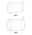
- 8A and 8B are perspective views of a light guide rod according to a modification of the embodiment of the present invention.
- SPFS apparatus surface plasmon enhanced fluorescence measuring apparatus
- SPR surface plasmon resonance
- the SPFS device is used in a state in which a detection chip having a prism made of a dielectric and a metal film formed on one surface of the prism is mounted.
- a capture body for capturing the substance to be detected is fixed on the metal film.
- the substance to be detected is captured by the capturing body.
- the substance to be detected may be labeled with a fluorescent substance or may not be labeled.
- the captured substance to be detected is further labeled with a fluorescent substance.
- the excitation light is irradiated so that the prism having the metal film on the surface satisfies the total reflection condition.
- interaction surface plasmon resonance
- this localized field light is also called “enhanced electric field” or “enhanced evanescent light”, and it is possible to measure a physical quantity variation in the vicinity of the surface of the metal film.
- This localized field light selectively excites the fluorescent substance that labels the substance to be detected captured on the metal film, and the fluorescence emitted from the fluorescent substance is observed.
- the SPFS device detects the presence or amount of a substance to be detected by measuring the amount of fluorescent light.
- FIG. 1 is a diagram showing a configuration of an SPFS apparatus 100 according to an embodiment of the present invention.
- the SPFS device 100 includes a chip holder 110 for detachably holding the detection chip 10, an excitation optical system unit 120 for irradiating the detection chip 10 with excitation light ⁇ , and a detection chip. 10 includes a light receiving optical system 140 for detecting light (plasmon scattered light ⁇ or fluorescence ⁇ ) emitted from the light source 10, and a control unit 160 for controlling them.
- the SPFS device 100 is used with the detection chip 10 mounted on the chip holder 110. Therefore, the detection chip 10 will be described first, and then each component of the SPFS device 100 will be described.
- the detection chip 10 includes a prism 20 having an incident surface 21, a film formation surface 22 and an emission surface 23, a metal film 30 formed on the film formation surface 22, and a film formation surface 22.
- a flow path lid 40 disposed on the metal film 30 is included.
- the detection chip 10 is replaced for each detection (analysis).
- the prism 20 is made of a dielectric that is transparent to the excitation light ⁇ .
- the prism 20 has an incident surface 21, a film forming surface 22, and an exit surface 23.
- the incident surface 21 causes the excitation light ⁇ from the excitation optical system unit 120 to enter the prism 20.
- a metal film 30 is formed on the film formation surface 22.
- the excitation light ⁇ incident on the inside of the prism 20 is reflected by the metal film 30. More specifically, the light is reflected at the interface (deposition surface 22) between the prism 20 and the metal film 30.
- the emission surface 23 emits the excitation light ⁇ reflected by the metal film 30 to the outside of the prism 20.
- the shape of the prism 20 is not particularly limited.
- the shape of the prism 20 is a column having a trapezoidal bottom surface.
- the surface corresponding to one base of the trapezoid is the film formation surface 22, the surface corresponding to one leg is the incident surface 21, and the surface corresponding to the other leg is the emission surface 23.
- the trapezoid serving as the bottom surface is preferably an isosceles trapezoid.
- the entrance surface 21 and the exit surface 23 are symmetric, and the S wave component of the excitation light ⁇ is less likely to stay in the prism 20.
- the incident surface 21 is formed so that the excitation light ⁇ does not return to the excitation optical system unit 120.
- the angle of the incident surface 21 is set so that the excitation light ⁇ does not enter the incident surface 21 perpendicularly in the scanning range centered on the ideal enhancement angle.
- the angle between the incident surface 21 and the film formation surface 22 and the angle between the film formation surface 22 and the emission surface 23 are both about 80 °.
- the material of the prism 20 include resin and glass.
- the material of the prism 20 is preferably a resin having a refractive index of 1.4 to 1.6 and a small birefringence.
- the metal film 30 is formed on the film formation surface 22 of the prism 20.
- an interaction surface plasmon resonance; SPR
- SPR surface plasmon resonance
- the material of the metal film 30 is not particularly limited as long as it is a metal that causes surface plasmon resonance.
- Examples of the material of the metal film 30 include gold, silver, copper, aluminum, and alloys thereof.
- the metal film 30 is a gold thin film.
- the method for forming the metal film 30 is not particularly limited. Examples of the method for forming the metal film 30 include sputtering, vapor deposition, and plating.
- the thickness of the metal film 30 is not particularly limited, but is preferably in the range of 30 to 70 nm.
- a capturing body for capturing a substance to be detected is fixed to a surface of the metal film 30 that does not face the prism 20. By fixing the capturing body, it becomes possible to selectively detect the substance to be detected.
- the detection target region 31 At least a part of the surface of the metal film 30 is set as the detection target region 31.
- the central portion of the surface of the metal film 30 is set as the detection target region 31.
- the capturing body is uniformly fixed in the detection target region 31.
- the “detection target region” refers to a region where a capturing body for capturing a substance to be detected is immobilized.
- the type of capturing body is not particularly limited as long as it can capture the substance to be detected.
- the capturing body is an antibody or a fragment thereof that can specifically bind to the substance to be detected.
- the channel lid 40 is disposed on the surface of the metal film 30 that does not face the prism 20 with the channel 41 interposed therebetween.
- the channel lid 40 may be disposed on the film formation surface 22 with the channel 41 interposed therebetween.
- the channel lid 40 and the metal film 30 (and the prism 20) form a channel 41 through which a liquid such as a specimen, a fluorescent labeling solution, and a cleaning solution flows.
- the detection target region 31 is exposed in the flow path 41. Both ends of the channel 41 are connected to an inlet and an outlet (both not shown) formed on the upper surface of the channel lid 40, respectively. When liquids are injected into the flow channel 41, these liquids contact the capturing body in the detection target region 31 in the flow channel 41.
- the channel lid 40 is made of a material that is transparent to light (plasmon scattered light ⁇ and fluorescence ⁇ ) emitted from the detection target region 31 of the metal film 30.
- An example of the material of the flow path lid 40 includes a resin. If these lights can be guided to the light receiving optical system 140, a part of the flow path lid 40 may be formed of an opaque material.
- the channel lid 40 is bonded to the metal film 30 or the prism 20 by, for example, adhesion using a double-sided tape or an adhesive, laser welding, ultrasonic welding, or pressure bonding using a clamp member.
- the excitation light ⁇ guided to the prism 20 enters the prism 20 through the incident surface 21.
- the excitation light ⁇ incident on the prism 20 is incident on the interface (deposition surface 22) between the prism 20 and the metal film 30 so as to have a total reflection angle (an angle at which surface plasmon resonance occurs).
- the reflected light from the interface is emitted out of the prism 20 at the emission surface 23 (not shown).
- plasmon scattered light ⁇ and fluorescence ⁇ are emitted from the detection target region 31 toward the light receiving optical system 140.
- the SPFS apparatus 100 includes the chip holder 110, the excitation optical system unit 120, the light receiving optical system 140, and the control unit 160.
- the chip holder 110 holds the detection chip 10 at a predetermined position.
- the detection chip 10 is irradiated with the excitation light ⁇ from the excitation optical system unit 120 while being held by the chip holder 110.
- plasmon scattered light ⁇ having the same wavelength as the excitation light ⁇ , fluorescence ⁇ emitted from the fluorescent material, and the like are emitted upward.
- the excitation light ⁇ is reflected at the interface between the prism 20 and the metal film 30 and is emitted to the outside of the prism 20 (not shown).
- the excitation optical system unit 120 includes a light source unit 121 that emits excitation light ⁇ , and an angle adjustment unit 122 that adjusts the incident angle of the excitation light ⁇ with respect to the interface (film formation surface 22) between the prism 20 and the metal film 30.
- the light source unit 121 includes a laser diode (hereinafter also referred to as “LD”) as an excitation light source, and excitation light ⁇ (single mode laser light) is directed toward the incident surface 21 of the prism 20 of the detection chip 10 held by the chip holder 110. ). More specifically, the light source unit 121 emits the excitation light ⁇ to the back surface of the metal film 30 corresponding to the region where the capturing body is fixed from the prism 20 side of the detection chip 10 so as to have a total reflection angle. .
- the light source unit 121 includes an LD unit, a wave rectifier, and a shaping optical system (all not shown).
- the LD unit emits the collimated excitation light ⁇ having a constant wavelength and light amount so that the shape of the irradiation spot at the interface (deposition surface 22) between the prism 20 and the metal film 30 is substantially circular.
- the LD unit includes an LD as an excitation light source, a collimator that collimates the excitation light ⁇ emitted from the LD, and a temperature adjustment circuit for making the light amount of the excitation light ⁇ constant.
- the excitation light ⁇ emitted from the LD has a flat outline shape even when collimated.
- the LD is held in a predetermined posture or a slit having a predetermined shape is inserted into a shaping optical system, which will be described later, so that the shape of the irradiation spot at the interface (deposition surface 22) is substantially circular.
- the wavelength and light amount of the excitation light ⁇ emitted from the LD vary depending on the temperature.
- the temperature adjustment circuit monitors the amount of light branched from the collimated excitation light ⁇ with a photodiode or the like, and installs a heater or a Peltier element so that the wavelength and amount of the excitation light ⁇ are constant. Use to adjust LD temperature.
- the wave shaper includes a band pass filter (hereinafter also referred to as “BPF”) and a linear polarization filter (hereinafter also referred to as “LP”), and tunes the excitation light ⁇ emitted from the LD unit. Since the excitation light ⁇ from the LD unit has a slight wavelength distribution width, the BPF turns the excitation light ⁇ from the LD unit into a narrow band light having only the center wavelength. In addition, since the excitation light ⁇ from the LD unit is not completely linearly polarized light, the LP converts the excitation light ⁇ from the LD unit into completely linearly polarized light.
- the wave tuner may include a half-wave plate that adjusts the polarization direction of the excitation light ⁇ so that the P-wave component is incident on the metal film 30.
- the shaping optical system adjusts the beam diameter, contour shape, and the like of the excitation light ⁇ so that the shape of the irradiation spot at the interface (deposition surface 22) between the prism 20 and the metal film 30 is a predetermined size.
- the excitation light ⁇ emitted from the shaping optical system is applied to the prism 20 of the detection chip 10.
- the shaping optical system is, for example, a slit or zoom means.
- the size of the irradiation spot of the excitation light ⁇ on one surface of the metal film 30 (surface facing the prism 20) is larger than that of the detection target region 31 on the other surface of the metal film 30 (surface facing the light guide rod 141). Is adjusted to be smaller. In this way, even if the irradiation spot is slightly displaced due to an error in each parameter of the prism 20, it is possible to prevent the irradiation spot from deviating from the detection target region 31.
- the type of light source included in the light source unit 121 is not particularly limited, and may not be LD.
- Examples of light sources include light emitting diodes, mercury lamps, and other laser light sources.
- the light emitted from the light source is not a beam
- the light emitted from the light source is converted into a beam by a lens, a mirror, a slit, or the like.
- the light emitted from the light source is not monochromatic light
- the light emitted from the light source is converted into monochromatic light by a diffraction grating or the like.
- the light emitted from the light source is not linearly polarized light
- the light emitted from the light source is converted into linearly polarized light by a polarizer or the like.
- the angle adjusting unit 122 adjusts the incident angle of the excitation light ⁇ to the metal film 30 (the interface between the prism 20 and the metal film 30 (film formation surface 22)).
- the angle adjusting unit 122 irradiates the excitation light ⁇ to a predetermined position (the back side of the detection target region 31) of the metal film 30 (deposition surface 22) at a predetermined incident angle, and the optical axis of the excitation light ⁇ and the chip.
- the holder 110 is rotated relatively.
- the angle adjustment unit 122 rotates the light source unit 121 around an axis orthogonal to the optical axis of the excitation light ⁇ .
- the position of the rotation axis is set so that the irradiation position on the metal film 30 (deposition surface 22) hardly moves even when the incident angle is scanned.
- the position of the rotation center is set near the intersection of the optical axes of the two excitation lights ⁇ at both ends of the scanning range of the incident angle (between the irradiation position on the film forming surface 22 and the incident surface 21 of the prism 20).
- the deviation of the irradiation position can be minimized.
- the light receiving optical system 140 is disposed so as to face a surface (detection target region 31) of the metal film 30 of the detection chip 10 held by the chip holder 110 that does not face the prism 20.
- the light receiving optical system 140 detects light (plasmon scattered light ⁇ or fluorescence ⁇ ) emitted from the metal film 30.
- the light receiving optical system 140 includes a light guide rod 141, a wavelength separation filter 144, and an optical sensor 145.
- the light guide rod 141 has an entrance surface 142 and an exit surface 143.
- the light guide rod 141 has translucency and guides light (plasmon scattered light ⁇ or fluorescence ⁇ ) emitted from the detection target region 31 (the metal film 30 and the vicinity thereof) to the optical sensor 145.
- the light guide rod 141 is formed in a predetermined shape and size. Details of the light guide rod 141 will be described later.
- the wavelength separation filter 144 transmits light in a predetermined wavelength region and blocks light in other wavelength regions (wavelength separation characteristic).
- the wavelength separation filter 144 is, for example, a long pass filter or a band pass filter. In the present embodiment, the wavelength separation filter 144 is a long pass filter.
- the wavelength separation filter 144 preferably blocks only the fluorescence ⁇ while blocking the light having the wavelength of the excitation light ⁇ (plasmon scattered light ⁇ ). As will be described later, the wavelength separation characteristic of the wavelength separation filter 144 has angle dependency.
- the wavelength separation filter 144 is disposed between the chip holder 110 (detection chip 10) and the light guide rod 141, or between the light guide rod 141 and the optical sensor 145, perpendicular to the axial direction of the light guide rod 141. .
- the wavelength separation filter 144 is disposed between the light guide rod 141 and the optical sensor 145.
- the axial direction of the light guide rod 141 refers to a direction from the center of gravity of the incident surface 142 of the light guide rod 141 toward the center of gravity of the exit surface 143.
- the wavelength separation filter 144 is configured to be movable between the optical path of the light receiving optical system 140 and the outside of the optical path by the filter control unit 164.
- the type of the wavelength separation filter 144 is not particularly limited as long as it transmits the fluorescent ⁇ , can separate unnecessary light other than the fluorescent ⁇ , and the wavelength separation characteristic of the filter has angle dependency.
- An example of the wavelength separation filter 144 in which the wavelength separation characteristic of the filter has an angle dependency includes an interference filter including one or more dielectric multilayer films. Details of the wavelength separation filter 144 will be described later.
- the optical sensor 145 detects light (fluorescence ⁇ or plasmon scattered light ⁇ ) emitted from the detection target region 31.
- the optical sensor 145 has a light receiving surface 146 that is perpendicular to the axial direction of the light guide rod 141.
- the optical sensor 145 detects light that is guided by the light guide rod 141 and reaches the light receiving surface 146.
- the type of the optical sensor 145 is not particularly limited as long as weak fluorescence ⁇ can be detected.
- the type of the photosensor 145 is, for example, a photomultiplier tube or an avalanche photodiode (APD) having a high sensitivity and a high S / N ratio.
- APD avalanche photodiode
- the control unit 160 performs control of each driving unit, quantification of the amount of light received by the optical sensor 145, and the like.
- the control unit 160 includes a light source control unit 161 that controls the light source unit 121, an optical sensor control unit 162 that controls the optical sensor 145, and a filter control unit 164 that controls a filter moving unit (not shown). And a control processing unit 163.
- the control processing unit 163 comprehensively controls the light source control unit 161, the optical sensor control unit 162, and the filter control unit 164 to control the overall operation of the SPFS apparatus 100.
- the control unit 160 is, for example, a computer that executes software.
- FIG. 2 is a diagram illustrating a positional relationship among the detection target region 31, the light guide rod 141, and the light receiving surface 146 of the optical sensor 145.
- the light guide rod 141 has translucency, allows light (plasmon scattered light ⁇ or fluorescence ⁇ ) emitted from the detection target region 31 to be incident on an incident surface 142 located at one end, and an exit surface located at the other end. The light is emitted at 143 and guided to the optical sensor 145.
- the shape of the light guide rod 141 is not particularly limited as long as the light emitted from the detection target region 31 can be guided to the optical sensor 145.
- the shape of the light guide rod 141 is a cylindrical shape having a constant cross-sectional area from the incident surface 142 toward the output surface 143 in a cross section orthogonal to the axial direction of the light guide rod 141.
- the material of the light guide rod 141 is not particularly limited as long as the plasmon scattered light ⁇ or the fluorescence ⁇ emitted from the detection target region 31 can be guided to the optical sensor 145.
- Examples of the material of the light guide rod 141 include transparent resin and transparent glass.
- the refractive index of the light guide rod 141 is not particularly limited, but is preferably about 1.4 to 2.0.
- a reflective film for preventing leakage of fluorescence ⁇ incident on the incident surface 142 of the light guide rod 141 may be formed on the side surface of the light guide rod 141.
- the reflective film is, for example, a vapor deposition film such as aluminum or gold.
- the incident surface 142 of the light guide rod 141 is one end surface (bottom surface) of the cylinder, and is disposed to face the surface of the metal film 30 (detection target region 31).
- the distance between the incident surface 142 of the light guide rod 141 and the detection target region 31 is about 0.5 to 5.0 mm.
- the diameter D of the incident surface 142 of the light guide rod 141 is longer than the maximum length D ′ of the detection target region 31.
- the “maximum length of the detection target area” refers to the length of the longest line segment among the line segments having two ends on the outer edge of the detection target area 31.
- the maximum length D ′ of the detection target region 31 is a diameter.
- the maximum length D ′ of the detection target region 31 is a diagonal length.
- the emission surface 143 is the other end surface (bottom surface) of the cylinder, and is disposed to face the light receiving surface 146 of the optical sensor 145 (or the wavelength separation filter 144 disposed in front thereof).
- the distance between the emission surface 143 and the light receiving surface 146 of the optical sensor 145 is about 0.5 to 5.0 mm.
- the diameter D of the exit surface 143 of the light guide rod 141 is preferably shorter than the maximum length D ′′ of the light receiving surface 146 of the optical sensor 145.
- the “maximum length of the light receiving surface” means the light reception of the optical sensor 145. It means the length of the longest line segment among the line segments having two points on the outer edge of the surface 146 as both ends.
- FIG. 3A is a schematic diagram showing an incident angle ⁇ 1 and a refraction angle ⁇ 2 of a light beam incident on the light guide rod 141.
- FIG. 3B is a graph showing the relationship between the incident angle ⁇ 1 and the refraction angle ⁇ 2.
- each light guide rod 141 having a refractive index n2 of 1.4, 1.5, 1.6, 1.7, 1.8, or 2.0 the incident angle ⁇ 1 is set to 0 to 90.
- the relationship between the incident angle ⁇ 1 and the refraction angle ⁇ 2 in each light guide rod 141 is shown in FIG. 3B.
- the uppermost curve shows the result when the light guide rod 141 having a refractive index n2 of 1.4 is used.
- the second curve from the top shows the result when the light guide rod 141 having a refractive index n2 of 1.5 is used.
- the third curve (thin broken line) from the top shows the result when the light guide rod 141 having a refractive index n2 of 1.6 is used.
- the fourth curve from the top shows the result when the light guide rod 141 having a refractive index n2 of 1.7 is used.
- the fifth curve (thin alternate long and short dash line) from the top shows the result when the light guide rod 141 having a refractive index n2 of 1.8 is used.
- the sixth curve from the top (thick one-dot chain line) shows the result when the light guide rod 141 having a refractive index n2 of 1.9 is used.
- the lowermost curve shows the result when the light guide rod 141 having a refractive index n2 of 2.0 is used.
- the rate of change of the refraction angle ⁇ 2 decreases as the incident angle ⁇ 1 increases.
- the maximum angle of the refraction angle ⁇ 2 is 45 °
- the light beam has a refraction angle ⁇ 2 in the range of 30 to 45 °.
- the density increases.
- the refractive angle ⁇ 2 decreases as the refractive index n2 of the light guide rod 141 increases.
- FIG. 4 is a diagram showing an optical path of a part of the fluorescent ⁇ that travels in the light guide rod 141.
- FIG. 4A is a diagram illustrating a difference in the optical path of the fluorescence ⁇ in the light guide rod 141 due to a difference in the incident position of the fluorescence ⁇
- FIG. 4B is a diagram of the fluorescence in the light guide rod 141 due to a difference in the refractive index n2 of the light guide rod 141. It is a figure which shows the difference in the optical path of (gamma).
- the optical path of fluorescence ⁇ having a high light density and a refraction angle ⁇ 2 of 45 ° will be considered.
- the solid arrow in FIG. 4A indicates the optical path of the fluorescent ⁇ incident at the center of the incident surface 142 of the light guide rod 141.
- a broken line arrow indicates an optical path of the fluorescent ⁇ incident at a position other than the center of the incident surface 142 of the light guide rod 141.
- the fluorescent light ⁇ is incident at a position shifted from the center of the incident surface 142 of the light guide rod 141 and the refraction angle ⁇ 2 is 45 °, and the diameter of the incident surface 142 is D. In this case, it can be seen that it passes through the center in the radial direction in the vicinity of the position D away from the incident surface 142.
- the solid line arrow in FIG. 4B indicates the optical path of the fluorescent ⁇ traveling through the light guide rod 141 having a refractive index n2 of 1.4.
- the broken line arrow indicates the optical path of the fluorescent ⁇ traveling through the light guide rod 141 having a refractive index n2 of 1.8.
- the fluorescent light ⁇ incident at the center of the incident surface 142 of the light guide rod 141 having a refractive index n2 of 1.4 and having a refraction angle ⁇ 2 of 45 ° is the diameter of the incident surface 142.
- D it can be seen that it passes through the center in the radial direction at a position away from the incident surface 142 by D.
- the fluorescence ⁇ incident at the center of the incident surface 142 of the light guide rod 141 having a refractive index n2 of 1.8 is incident when the diameter of the incident surface 142 is D.
- the light guide rod 141 of the SPFS device 100 is based on the refractive index n2 of the light guide rod 141 and the diameter D of the light guide rod 141 so as to satisfy the formula (1).
- a length L is defined.
- Fluorescence ⁇ emitted from the exit surface 143 of the light guide rod 141 reaches the light receiving surface 146 of the optical sensor 145.
- the incident angle at which the amount of light is the largest is referred to as a peak incident angle.
- the light density increases within the range of the refraction angle ⁇ 2 of 30 to 45 °.
- the exit angle at which the amount of light increases most on the exit surface 143 of the light guide rod 141 is a predetermined angle other than 0 ° (for example, 35 °), and the peak incident angle on the light receiving surface 146 of the optical sensor 145 is also 0 °.
- the wavelength separation filter 144 and the light receiving surface 146 of the optical sensor 145 are both disposed perpendicular to the axial direction of the light guide rod 141.
- the incident angle of the light beam that is emitted from the output surface 143 of the light guide rod 141 and incident on the wavelength separation filter 144, and the incident angle of the light beam that passes through the wavelength separation filter 144 and is incident on the light receiving surface 146 of the optical sensor 145 are the same. That is, the peak incident angle in the wavelength separation filter 144 is also a predetermined angle other than 0 ° (for example, 35 °).
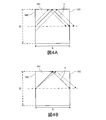
- FIG. 5 is a diagram for explaining the angle dependency of the wavelength separation characteristic of the wavelength separation filter 144 (long pass filter) used in the present embodiment.
- FIG. 5A is a diagram illustrating the wavelength separation characteristics of the wavelength separation filter 144 with respect to light incident at a peak incident angle (for example, 35 °), and
- FIG. 5B illustrates the wavelength separation filter 144 with respect to light incident at an incident angle of 0 °. It is a figure which shows a wavelength separation characteristic.
- the solid line represents the wavelength separation filter 144 having a cutoff wavelength of 640 nm for a light beam having an incident angle of the peak incident angle (35 °) and a cutoff wavelength of 680 nm for a light beam having an incident angle of 0 °.
- the light transmittance is shown.
- the alternate long and short dash line indicates the spectrum of the excitation light ⁇ having a dominant wavelength of 635 nm
- the alternate long and two short dashes line indicates a spectrum of fluorescence ⁇ having a dominant wavelength of 670 nm.
- the “excitation light” includes not only the excitation light ⁇ but also light having the same wavelength as the excitation light ⁇ (plasmon scattered light ⁇ ).
- the cutoff wavelength (640 nm) of the wavelength separation filter 144 is incident at the main wavelength (635 nm) and the peak incident angle (35 °) of the excitation light ⁇ incident at the peak incident angle (35 °). It is located between the dominant wavelength (670 nm) of the fluorescent ⁇ . That is, the light transmittance of the wavelength separation filter 144 at the main wavelength (670 nm) with respect to the fluorescent ⁇ light beam incident at the peak incident angle (35 °) is the main light beam of the excitation light ⁇ incident at the peak incident angle (35 °). It is larger than the light transmittance of the wavelength separation filter 144 at the wavelength (635 nm).
- the wavelength separation filter 144 selectively transmits the fluorescence ⁇ with respect to the light incident at the peak incident angle (35 °), and blocks most of the excitation light ⁇ . Therefore, as described above, since the incident angle of the light beam to the wavelength separation filter 144 and the incident angle of the light beam to the light receiving surface 146 of the optical sensor 145 are the same, the wavelength separation filter 144 is applied to the light receiving surface 146 of the optical sensor 145. Most of the fluorescence ⁇ incident at the peak incident angle (35 °) can be selectively transmitted.
- the cutoff wavelength (680 nm) of the wavelength separation filter 144 for the light incident at an incident angle of 0 ° is compared to the light incident at the peak incident angle (35 °). , Shifted to the long wavelength side.
- the wavelength separation filter 144 long pass filter
- the wavelength separation filter 144 can more reliably block the excitation light ⁇ .
- the wavelength separation filter 144 may block not only the excitation light ⁇ but also a part of the fluorescence ⁇ .
- the S / N ratio can be improved by more surely blocking the excitation light ⁇ .
- the wavelength separation characteristic of the wavelength separation filter 144 used in the present embodiment has an angle dependency, and is optimized for a light ray incident at a peak incident angle (35 °). . That is, the light transmittance (hereinafter also referred to as “T t ”) of the wavelength separation filter 144 at the principal wavelength with respect to the fluorescent ⁇ light beam incident at the peak incident angle is the main transmittance with respect to the fluorescent ⁇ light beam incident at an incident angle of 0 °. It is larger than the light transmittance (hereinafter also referred to as “T 0 ”) of the wavelength separation filter 144 at a wavelength (T t > T 0 ). Therefore, as described above, the efficiency and the SN ratio can be improved.
- a wavelength separation filter 144 having a cutoff wavelength longer than the main wavelength of the excitation light ⁇ may be used. This is because even if the transmittance of the fluorescent ⁇ decreases, an improvement in the SN ratio can be expected by blocking the excitation light ⁇ more reliably. For example, it is preferable that T 0 / T t ⁇ 1/5.
- the parameters for the simulation are as follows: the height of the channel lid 40: 0.1 mm, the refractive index of the channel lid 40 (PMMA): 1.49, the maximum length D ′ of the detection target region 31: 3.0 mm, The length of the light guide rod 141 in the axial direction: 16.0 mm, the diameter D of the light guide rod 141: 14.0 mm, the refractive index n of the light guide rod 141: 1.514, the detection target region 31 and the light guide rod 141 The interval between the incident surfaces 142 is 0.6 mm, the length (thickness) of the wavelength separation filter in the axial direction of the light guide rod 141 is 1.0 mm, the refractive index of the wavelength separation filter 144 is 1.514, and the light guide rod 141 The length (thickness) of the sensor window in the axial direction: 0.8 mm, the refractive index of the sensor window (borosilicate glass): 1.487, the distance between the wavelength separation filter 144 and the sensor window: 0.5 mm, the
- FIG. 6 is a diagram illustrating a simulation result of the relationship between the incident angle of the fluorescent light ⁇ and the light amount on the light receiving surface 146 of the optical sensor 145.
- the fluorescence ⁇ emitted from the detection target region 31 has the largest amount of light when entering the light receiving surface 146 with an incident angle near 35 °. Therefore, in this case, the light transmittance (T t ) of the wavelength separation filter 144 at the principal wavelength with respect to the light beam of the fluorescent ⁇ incident on the light receiving surface 146 at an incident angle of 35 ° (peak incident angle) has an incident angle of 35 °.
- the wavelength separation at the principal wavelength with respect to the light beam of the fluorescence ⁇ that is larger than the light transmittance of the wavelength separation filter 144 at the principal wavelength with respect to the light beam of the excitation light incident on the light receiving surface 146 and the incident angle is 0 °.
- the wavelength separation filter 144 is selected so as to be larger than the light transmittance (T 0 ) of the filter 144.
- the light transmittance of the wavelength separation filter 144 at the main wavelength with respect to the light beam of the fluorescent ⁇ incident on the wavelength separation filter 144 at an incident angle of 35 ° is an excitation incident on the wavelength separation filter 144 at an incident angle of 35 °.
- the wavelength separation filter 144 is selected so as to increase. As a result, the wavelength separation filter 144 can block the excitation light ⁇ and selectively transmit the fluorescence ⁇ with respect to the light incident on the light receiving surface 146 at the peak incident angle.
- the wavelength separation filter 144 may block a part of the fluorescence ⁇ with respect to the light incident on the light receiving surface 146 with an incident angle of 0 °, it also blocks the excitation light ⁇ more reliably. Can do.
- the SPFS device 100 can detect the fluorescence ⁇ efficiently and with a high S / N ratio.
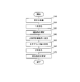
- FIG. 7 is a flowchart illustrating an example of an operation procedure of the SPFS apparatus.
- step S10 preparation for measurement is performed (step S10). Specifically, the detection chip 10 including the detection target region 31 on which the capturing body for capturing the detection target substance is fixed is installed at a predetermined position of the SPFS device 100. Further, when the storage reagent is present in the flow channel 41 of the detection chip 10, the storage reagent is removed by washing the flow channel 41 so that the capturing body can appropriately capture the substance to be detected.
- the substance to be detected in the sample and the capturing body are reacted (primary reaction, step S20). Specifically, the specimen is injected into the flow path 41, and the specimen and the capturing body are brought into contact with each other. When the substance to be detected is present in the specimen, at least a part of the substance to be detected is captured by the capturing body. Thereafter, the inside of the flow path 41 is washed with a buffer solution or the like to remove substances not captured by the capturing body.
- the type of specimen is not particularly limited. Examples of the specimen include body fluids such as blood, serum, plasma, urine, nasal fluid, saliva, semen, and diluted solutions thereof.
- the control processing unit 163 controls the light source unit 121 and the angle adjusting unit 122 to irradiate a predetermined position of the metal film 30 (deposition surface 22) with the excitation light ⁇ , while the metal film 30 ( The incident angle of the excitation light ⁇ with respect to the film forming surface 22) is scanned.
- control processing unit 163 controls the filter control unit 164 so that the optical sensor 145 detects the plasmon scattered light ⁇ from the detection target region 31, so that the wavelength separation filter 144 is out of the optical path of the light receiving optical system 140.
- the optical sensor control unit 162 is controlled so as to move and detect the plasmon scattered light ⁇ . Plasmon scattered light ⁇ from the detection target region 31 reaches the optical sensor 145 through the light guide rod 141. As a result, the control processing unit 163 obtains data including the relationship between the incident angle of the excitation light ⁇ and the intensity of the plasmon scattered light ⁇ .
- the control processing unit 163 analyzes the data and determines an incident angle (intensification angle) that maximizes the intensity of the plasmon scattered light ⁇ .
- the enhancement angle is basically determined by the material and shape of the prism 20, the thickness of the metal film 30, the refractive index of the liquid in the channel 41, etc., but the type and amount of the fluorescent substance in the channel 41, It varies slightly due to various factors such as the shape error of the prism 20. For this reason, it is preferable to determine the enhancement angle each time analysis is performed.
- the enhancement angle is determined on the order of about 0.1 °.
- the incident angle of the excitation light ⁇ with respect to the metal film 30 (deposition surface 22) is set to the enhancement angle determined in the previous step (step S40). Specifically, the control processing unit 163 controls the angle adjustment unit 122 to set the incident angle of the excitation light ⁇ with respect to the metal film 30 (deposition surface 22) as an enhancement angle. In the subsequent steps, the incident angle of the excitation light ⁇ with respect to the metal film 30 (deposition surface 22) remains the enhancement angle.
- the excitation light ⁇ is irradiated onto the metal film 30 (deposition surface 22), and the intensity (optical blank value) of light having the same wavelength as the fluorescence ⁇ is measured (step S50).
- the control processing unit 163 controls the filter control unit 164 that controls the filter moving unit to move the wavelength separation filter 144 on the optical path of the light receiving optical system 140.
- the control processing unit 163 controls the light source control unit 161 to cause the light source unit 121 to emit the excitation light ⁇ .
- the control processing unit 163 controls the optical sensor control unit 162 so that the optical sensor 145 detects the intensity of light having the same wavelength as the fluorescence ⁇ . Therefore, the optical sensor 145 can accurately measure the intensity (optical blank value) of light that becomes noise.
- the measured value is transmitted to the control processing unit 163 and recorded as an optical blank value.
- the detected substance captured by the capturing body is labeled with a fluorescent substance (secondary reaction, step S60).
- a fluorescent labeling solution is injected into the channel 41.
- the fluorescent labeling solution is, for example, a buffer solution containing an antibody (secondary antibody) labeled with a fluorescent substance.
- the fluorescent labeling liquid comes into contact with the substance to be detected, and the target substance is labeled with the fluorescent substance. Thereafter, the inside of the flow path 41 is washed with a buffer solution or the like to remove free fluorescent substances.
- the excitation light ⁇ is irradiated onto the metal film 30 (deposition surface 22), the intensity of the fluorescence ⁇ (weak light) emitted from the detection target region 31 (labeling substance) and guided by the light guide rod 141 is increased. It measures with the optical sensor 145 (process S70).
- the control processing unit 163 controls the light source control unit 161 to cause the light source unit 121 to emit the excitation light ⁇ .
- the control processing unit 163 controls the optical sensor control unit 162 so that the optical sensor 145 detects the fluorescence ⁇ emitted from the detection target region 31.
- the control processing unit 163 subtracts the optical blank value from the measured value, and calculates the fluorescence intensity that correlates with the amount of the substance to be detected.
- the fluorescence intensity is converted into the amount or concentration of the substance to be detected as necessary.
- the diameter of the incident surface 142 of the light guide rod 141 is D
- the length of the cylindrical light guide rod 141 in the axial direction is L
- the light guide rod When the refractive index of 141 is n2, 0.8n2D ⁇ L ⁇ 1.2n2D is satisfied. Therefore, most of the fluorescence ⁇ emitted from the fluorescent material is condensed in the vicinity of the position away from the incident surface 142 of the light guide rod 141 by the diameter D of the light guide rod 141 and reaches the light receiving surface 146 of the optical sensor 145. To do.
- the fluorescence ⁇ reaching the light receiving surface 146 has the largest amount of light at a predetermined angle (peak incident angle) other than 0 °. Therefore, by optimizing the wavelength separation characteristic of the wavelength separation filter 144 with respect to the light incident on the light receiving surface 146 at the peak incident angle, the SPFS device 100 can be efficiently and at a high SN ratio without increasing the size. Fluorescence ⁇ can be detected.
- the wavelength separation filter 144 may be integrated with the light guide rod 141.
- the light guide rod 141 and the wavelength separation filter 144 may be integrated by forming a dielectric multilayer film on the entrance surface 142 or the exit surface 143 of the light guide rod 141.
- the SPFS apparatus 100 can be reduced in size and simplified.
- the SPFS device 100 having the columnar light guide rod 141 has been described, but the shape of the light guide rod 141 is not limited to a columnar shape.
- 8A and 8B are perspective views of light guide rods 141 ′ and 141 ′′ according to a modification of the embodiment of the present invention.
- the light guide rod is viewed from the incident surface as shown in FIG. 8A.
- a tapered light guide rod 141 ′ whose cross-sectional area continuously decreases toward the exit surface, or a tapered light guide rod 141 ′ whose cross-sectional area continuously increases from the entrance surface toward the exit surface. There may be.
- the optical sensor 145 having a small area of the light receiving surface 146 may be used. It can. From the viewpoint of downsizing and cost reduction of the detection device, it is preferable that an optical sensor 145 having a small area of the light receiving surface 146 can be used.
- the detection device that detects weak light can use the optical sensor 145 having a small area of the light receiving surface 146 from the viewpoint of detecting the fluorescence ⁇ with a high S / N ratio.
- the tapered light guide rod 141 ′ whose cross-sectional area continuously increases from the incident surface toward the output surface, the light incident on the incident surface is reflected by the tapered surface in the light guide rod 141 ′.
- the exit angle of the light beam emitted on the output surface with respect to the output surface can be reduced.
- the peak incident angle can be reduced as compared with the case where the cylindrical light guide rod 141 is used.
- the wavelength separation filter 144 that is optimized with respect to the light beam incident at the peak incident angle (35 °) has been described.
- the peak incident angle changes from 35 ° to 30 °.
- the cutoff wavelength changes from 640 nm to 680 nm, that is, shifts by 40 nm to the longer wavelength side (see FIGS. 5A and 5B).
- the cutoff wavelength is shifted only about 30 nm toward the long wavelength side. That is, if FIGS.
- 5A and 5B are diagrams showing the wavelength separation characteristics of the wavelength separation filter optimized for light incident at an incident angle of 30 °, the light incident on the incident light at an incident angle of 30 ° in FIG.
- the cutoff wavelength of the wavelength separation filter is 640 nm
- the cutoff wavelength of the wavelength separation filter for a light ray incident at an incident angle of 0 ° in FIG. 5B is 670 nm.
- the SPFS apparatus can detect more fluorescence ⁇ while reliably blocking the excitation light ⁇ , and can further improve the SN ratio.
- the light incident rod or light exit surface 141 ′′ may have a convex lens shape. Further, although not particularly illustrated, both the light incident surface and the light output surface have a convex lens shape.
- the fluorescence ⁇ emitted from the detection target region 31 can be efficiently collected on the light receiving surface 146 of the optical sensor 145. Therefore, the fluorescence ⁇ can be efficiently and at a high SN ratio. Can be detected.
- the order of the steps is limited to this.
- the enhancement angle may be measured before the primary reaction. Thereby, it is possible to avoid the enhancement angle from changing due to the influence of the substance adsorbed nonspecifically in the flow path of the detection chip by the primary reaction. If the incident angle of the excitation light ⁇ is determined in advance, the enhancement angle need not be measured.
- the detection chip 10 having the flow channel 41 is described as an example, but a detection chip having a well instead of the flow channel can also be used.
- the detection device can detect weak fluorescence emitted from a labeling substance efficiently and with a high S / N ratio, and thus is useful for clinical examinations, for example.
Landscapes
- Health & Medical Sciences (AREA)
- Immunology (AREA)
- Chemical & Material Sciences (AREA)
- Physics & Mathematics (AREA)
- Biochemistry (AREA)
- Nuclear Medicine, Radiotherapy & Molecular Imaging (AREA)
- Life Sciences & Earth Sciences (AREA)
- Analytical Chemistry (AREA)
- General Health & Medical Sciences (AREA)
- General Physics & Mathematics (AREA)
- Pathology (AREA)
- Optics & Photonics (AREA)
- Chemical Kinetics & Catalysis (AREA)
- Investigating, Analyzing Materials By Fluorescence Or Luminescence (AREA)
Abstract
Description
SPFS装置は、誘電体からなるプリズムと、プリズムの1面上に形成された金属膜とを有する検出チップが装着された状態で使用される。金属膜上には、被検出物質を捕捉するための捕捉体が固定されている。金属膜上に被検出物質を含む検体を提供すると、被検出物質が捕捉体により捕捉される。このとき、被検出物質は、蛍光物質で標識されていてもよいし、標識されていなくてもよい。捕捉された被検出物質が蛍光物質で標識されていない場合、捕捉された被検出物質は、さらに蛍光物質で標識される。この状態で、表面に金属膜を有するプリズムに対して全反射条件となるように励起光を照射する。これにより、励起光および金属膜中の自由電子の相互作用(表面プラズモン共鳴)が生じ、局在場光が発生する。一般にこの局在場光は、「増強電場」または「増強されたエバネッセント光」とも呼ばれ、金属膜の表面近傍の物理量変動を測定することが可能である。この局在場光により、金属膜上に捕捉された被検出物質を標識する蛍光物質が選択的に励起され、蛍光物質から放出された蛍光が観察される。SPFS装置は、蛍光の光量を測定して、被検出物質の存在またはその量を検出する。
次に、導光ロッド141について詳細に説明する。図2は、検出対象領域31、導光ロッド141および光センサー145の受光面146の位置関係を示す図である。
0.8n2D<L<1.2n2D …(1)
次に、本実施の形態で使用する波長分離フィルター144の波長分離特性について説明する。図5は、本実施の形態で使用する波長分離フィルター144(ロングパスフィルター)の波長分離特性の角度依存性を説明するための図である。図5Aは、ピーク入射角(例えば35°)で入射する光線に対する波長分離フィルター144の波長分離特性を示す図であり、図5Bは、入射角が0°で入射する光線に対する波長分離フィルター144の波長分離特性を示す図である。図5Aおよび図5Bにおいて、実線は、入射角がピーク入射角(35°)の光線に対するカットオフ波長が640nmであり、入射角が0°の光線に対するカットオフ波長が680nmである波長分離フィルター144の光透過率を示す。また、一点鎖線は、主波長が635nmである励起光αのスペクトルを示し、二点鎖線は、主波長が670nmである蛍光γのスペクトルを示す。ここで、「励起光」とは、励起光αだけでなく励起光αと同じ波長の光(プラズモン散乱光β)を含むものとする。
本実施の形態に係るSPFS装置100において、光センサー145の受光面146における蛍光γの入射角と光量との関係についてシミュレーションを行った。流路41内の検出対象領域31から受光面146までの光路上には、流路蓋40、導光ロッド141、波長分離フィルター144および光センサー145が、検出対象領域31側から順番に配置されている。また、導光ロッド141の出射面143で出射した光は、波長分離フィルター144を通過したあと、センサー窓を通って受光面146に到達する。シミュレーションのための各パラメータは、流路蓋40の高さ:0.1mm、流路蓋40(PMMA)の屈折率:1.49、検出対象領域31の最大長さD’:3.0mm、導光ロッド141の軸方向の長さ:16.0mm、導光ロッド141の直径D:14.0mm、導光ロッド141の屈折率n:1.514、検出対象領域31および導光ロッド141の入射面142の間隔:0.6mm、導光ロッド141の軸方向での波長分離フィルターの長さ(厚み):1.0mm、波長分離フィルター144の屈折率:1.514、導光ロッド141の軸方向でのセンサー窓の長さ(厚み):0.8mm、センサー窓(ホウケイ酸ガラス)の屈折率:1.487、波長分離フィルター144およびセンサー窓の間隔:0.5mm、受光面146の最大長さ:8.0mmとした。
次に、SPFS装置100の動作(SPFS装置100を用いた検出方法)について説明する。図7は、SPFS装置の動作手順の一例を示すフローチャートである。
20 プリズム
21 プリズムの入射面
22 プリズムの成膜面
23 プリズムの出射面
30 金属膜
31 検出対象領域
40 流路蓋
41 流路
100 表面プラズモン共鳴蛍光分析装置(SPFS装置)
110 チップホルダー
120 励起光学系ユニット
121 光源ユニット
122 角度調整部
140 受光光学系
141、141’、141” 導光ロッド
142 導光ロッドの入射面
143 導光ロッドの出射面
144 波長分離フィルター
145 光センサー
146 受光面
160 制御部
161 光源制御部
162 光センサー制御部
163 制御処理部
164 フィルター制御部
θ1 導光ロッドに入射する光線の入射角
θ2 導光ロッドに入射した光線の屈折角
n1、n2 屈折率
D 導光ロッドの直径
D’ 検出対象領域の最大長さ
D” 光センサーの受光面の最大長さ
L 導光ロッドの軸方向の長さ
α 励起光
β プラズモン散乱光
γ 蛍光
Claims (7)
- 被検出物質を標識した蛍光物質から放出される蛍光を検出することにより、前記被検出物質を検出する検出装置であって、
前記被検出物質を捕捉するための捕捉体が固定化された検出対象領域を含む検出チップを保持するチップホルダーと、
前記チップホルダーに保持された前記検出チップに励起光を照射するための光源と、
前記捕捉体に捕捉された前記被検出物質を標識した蛍光物質から放出される蛍光を、一端に位置する入射面で入射させ、他端に位置する出射面で出射させる導光ロッドと、
前記導光ロッドの軸方向に対して垂直な受光面を有し、前記蛍光を検出するための光センサーと、
前記検出チップおよび前記導光ロッドの間、または前記導光ロッドおよび前記光センサーの間に前記導光ロッドの軸方向に対して垂直に配置され、前記蛍光と前記蛍光以外の不要な光とを分離するための波長分離フィルターと、
を有し、
前記受光面における前記蛍光の入射角と光量との関係において、最も光量が多い入射角であるピーク入射角は0°以外であり、
前記ピーク入射角で前記受光面に入射する前記蛍光の光線に対する主波長における前記波長分離フィルターの光透過率は、前記ピーク入射角で前記受光面に入射する前記励起光の光線に対する主波長における前記波長分離フィルターの光透過率よりも大きく、かつ入射角が0°で前記受光面に入射する前記蛍光の光線に対する主波長における前記波長分離フィルターの光透過率より大きい、
検出装置。 - 入射角が0°で前記受光面に入射する前記蛍光の光線に対する主波長における前記波長分離フィルターの光透過率は、前記ピーク入射角で前記受光面に入射する前記蛍光の光線に対する主波長における前記波長分離フィルターの光透過率の1/5以下である、請求項1に記載の検出装置。
- 前記波長分離フィルターは、前記導光ロッドと一体化されている、請求項1または請求項2に記載の検出装置。
- 前記導光ロッドは、前記入射面から前記出射面に向かってその断面積が一定である円柱状であり、
入射角が35°で前記受光面に入射する前記蛍光の光線に対する主波長における前記波長分離フィルターの光透過率は、入射角が35°で前記受光面に入射する前記励起光の光線に対する主波長における前記波長分離フィルターの光透過率よりも大きく、かつ入射角が0°で前記受光面に入射する前記蛍光の光線に対する主波長における前記波長分離フィルターの光透過率より大きい、
請求項1~3のいずれか一項に記載の検出装置。 - 入射角が35°で前記波長分離フィルターに入射する前記蛍光の光線に対する主波長における前記波長分離フィルターの光透過率は、入射角が35°で前記波長分離フィルターに入射する前記励起光の光線に対する主波長における前記波長分離フィルターの光透過率よりも大きく、かつ入射角が0°で前記波長分離フィルターに入射する前記蛍光の光線に対する主波長における前記波長分離フィルターの光透過率より大きい、請求項4に記載の検出装置。
- 前記導光ロッドは、前記入射面から前記出射面に向かってその断面積が連続的に小さくなるテーパー状の導光ロッド、前記入射面から前記出射面に向かってその断面積が連続的に大きくなるテーパー状の導光ロッド、または前記入射面、前記出射面もしくはこれら両方が凸レンズ状の導光ロッドである、請求項1~3のいずれか一項に記載の検出装置。
- 前記検出チップは、プリズムと、前記プリズム上に配置された金属膜とを有し、
前記検出対象領域は、前記金属膜の表面の少なくとも一部であり、
前記光源は、前記プリズム側から前記捕捉体が固定されている領域に対応した前記金属膜の裏面に励起光を照射し、
前記蛍光は、前記プリズムを介して前記金属膜の裏面に照射した励起光により生じる局在場光により励起され、前記蛍光物質から放出される蛍光である、
請求項1~6のいずれか一項に記載の検出装置。
Priority Applications (3)
| Application Number | Priority Date | Filing Date | Title |
|---|---|---|---|
| US15/320,099 US9726606B2 (en) | 2014-06-19 | 2015-06-16 | Detection device |
| EP15809717.0A EP3159677B1 (en) | 2014-06-19 | 2015-06-16 | Detection device |
| JP2016529343A JP6421821B2 (ja) | 2014-06-19 | 2015-06-16 | 検出装置 |
Applications Claiming Priority (2)
| Application Number | Priority Date | Filing Date | Title |
|---|---|---|---|
| JP2014126282 | 2014-06-19 | ||
| JP2014-126282 | 2014-06-19 |
Publications (1)
| Publication Number | Publication Date |
|---|---|
| WO2015194518A1 true WO2015194518A1 (ja) | 2015-12-23 |
Family
ID=54935503
Family Applications (1)
| Application Number | Title | Priority Date | Filing Date |
|---|---|---|---|
| PCT/JP2015/067222 Ceased WO2015194518A1 (ja) | 2014-06-19 | 2015-06-16 | 検出装置 |
Country Status (4)
| Country | Link |
|---|---|
| US (1) | US9726606B2 (ja) |
| EP (1) | EP3159677B1 (ja) |
| JP (1) | JP6421821B2 (ja) |
| WO (1) | WO2015194518A1 (ja) |
Cited By (1)
| Publication number | Priority date | Publication date | Assignee | Title |
|---|---|---|---|---|
| JP2017138306A (ja) * | 2016-01-31 | 2017-08-10 | アークレイ株式会社 | 分析用具および分析装置 |
Families Citing this family (3)
| Publication number | Priority date | Publication date | Assignee | Title |
|---|---|---|---|---|
| US10345239B1 (en) * | 2016-09-08 | 2019-07-09 | Verily Life Sciences Llc | Thin stackup for diffuse fluorescence system |
| EP3460456B1 (en) * | 2017-09-20 | 2020-08-26 | IMEC vzw | A biosensor system for detecting supercritical angle fluorescent light |
| EP3705875B1 (en) | 2019-03-05 | 2022-11-30 | IMEC vzw | An apparatus and method for detecting photoluminescent light emitted from a sample |
Citations (3)
| Publication number | Priority date | Publication date | Assignee | Title |
|---|---|---|---|---|
| JPH04203952A (ja) * | 1990-11-29 | 1992-07-24 | Fuji Xerox Co Ltd | ガス検知装置 |
| JP2004008412A (ja) * | 2002-06-05 | 2004-01-15 | Olympus Corp | 内視鏡装置用光源装置及び内視鏡装置 |
| JP2014032148A (ja) * | 2012-08-06 | 2014-02-20 | Arkray Inc | 表面プラズモン励起増強蛍光取得構造体および表面プラズモン励起増強蛍光測定システム |
Family Cites Families (7)
| Publication number | Priority date | Publication date | Assignee | Title |
|---|---|---|---|---|
| JPH11352409A (ja) * | 1998-06-05 | 1999-12-24 | Olympus Optical Co Ltd | 蛍光検出装置 |
| JP2000241350A (ja) * | 1999-02-17 | 2000-09-08 | Bunshi Biophotonics Kenkyusho:Kk | 蛍光観察装置評価方法および透過フィルタ |
| WO2009091902A1 (en) * | 2008-01-17 | 2009-07-23 | The Salk Institute For Biological Studies | 3d scanning acousto-optic microscope |
| GB0812926D0 (en) * | 2008-07-15 | 2008-08-20 | Assaymetrics Ltd | Spectrometer and method of operating a spectrometer |
| JP5104957B2 (ja) * | 2008-09-18 | 2012-12-19 | 株式会社島津製作所 | 蛍光画像検出装置及び蛍光画像検出方法 |
| WO2010101052A1 (ja) | 2009-03-03 | 2010-09-10 | コニカミノルタホールディングス株式会社 | 表面プラズモン増強蛍光センサおよび表面プラズモン増強蛍光センサに用いられる集光部材 |
| EP2579023B1 (en) * | 2010-06-04 | 2018-09-26 | Konica Minolta Holdings, Inc. | Surface plasmon resonance fluorescence analysis device and surface plasmon resonance fluorescence analysis method |
-
2015
- 2015-06-16 US US15/320,099 patent/US9726606B2/en active Active
- 2015-06-16 EP EP15809717.0A patent/EP3159677B1/en active Active
- 2015-06-16 JP JP2016529343A patent/JP6421821B2/ja active Active
- 2015-06-16 WO PCT/JP2015/067222 patent/WO2015194518A1/ja not_active Ceased
Patent Citations (3)
| Publication number | Priority date | Publication date | Assignee | Title |
|---|---|---|---|---|
| JPH04203952A (ja) * | 1990-11-29 | 1992-07-24 | Fuji Xerox Co Ltd | ガス検知装置 |
| JP2004008412A (ja) * | 2002-06-05 | 2004-01-15 | Olympus Corp | 内視鏡装置用光源装置及び内視鏡装置 |
| JP2014032148A (ja) * | 2012-08-06 | 2014-02-20 | Arkray Inc | 表面プラズモン励起増強蛍光取得構造体および表面プラズモン励起増強蛍光測定システム |
Non-Patent Citations (1)
| Title |
|---|
| See also references of EP3159677A4 * |
Cited By (1)
| Publication number | Priority date | Publication date | Assignee | Title |
|---|---|---|---|---|
| JP2017138306A (ja) * | 2016-01-31 | 2017-08-10 | アークレイ株式会社 | 分析用具および分析装置 |
Also Published As
| Publication number | Publication date |
|---|---|
| EP3159677B1 (en) | 2019-08-14 |
| JP6421821B2 (ja) | 2018-11-14 |
| US9726606B2 (en) | 2017-08-08 |
| EP3159677A1 (en) | 2017-04-26 |
| JPWO2015194518A1 (ja) | 2017-04-20 |
| EP3159677A4 (en) | 2018-02-21 |
| US20170138859A1 (en) | 2017-05-18 |
Similar Documents
| Publication | Publication Date | Title |
|---|---|---|
| JP6635168B2 (ja) | 表面プラズモン共鳴蛍光分析方法 | |
| US20200003688A1 (en) | Surface Plasmon Resonance Fluorescence Analysis Device And Surface Plasmon Resonance Fluorescence Analysis Method | |
| JP6369533B2 (ja) | 測定方法および測定装置 | |
| JP6587024B2 (ja) | 検出方法および検出装置 | |
| JP6421821B2 (ja) | 検出装置 | |
| JPWO2018034143A1 (ja) | 測定方法、測定装置および測定システム | |
| JPWO2018034208A1 (ja) | 測定方法 | |
| JPWO2018051863A1 (ja) | 測定方法 | |
| JP6221785B2 (ja) | 検出装置および検出方法 | |
| JP6954116B2 (ja) | 測定方法、測定装置および測定チップ | |
| JP6493412B2 (ja) | 検出装置および検出方法 | |
| JP6673336B2 (ja) | 検出装置 | |
| WO2016147774A1 (ja) | 測定方法および測定装置 |
Legal Events
| Date | Code | Title | Description |
|---|---|---|---|
| 121 | Ep: the epo has been informed by wipo that ep was designated in this application |
Ref document number: 15809717 Country of ref document: EP Kind code of ref document: A1 |
|
| ENP | Entry into the national phase |
Ref document number: 2016529343 Country of ref document: JP Kind code of ref document: A |
|
| REEP | Request for entry into the european phase |
Ref document number: 2015809717 Country of ref document: EP |
|
| WWE | Wipo information: entry into national phase |
Ref document number: 2015809717 Country of ref document: EP |
|
| NENP | Non-entry into the national phase |
Ref country code: DE |
|
| WWE | Wipo information: entry into national phase |
Ref document number: 15320099 Country of ref document: US |