WO2015198496A1 - はんだ合金、はんだ組成物、ソルダペーストおよび電子回路基板 - Google Patents
はんだ合金、はんだ組成物、ソルダペーストおよび電子回路基板 Download PDFInfo
- Publication number
- WO2015198496A1 WO2015198496A1 PCT/JP2014/072575 JP2014072575W WO2015198496A1 WO 2015198496 A1 WO2015198496 A1 WO 2015198496A1 JP 2014072575 W JP2014072575 W JP 2014072575W WO 2015198496 A1 WO2015198496 A1 WO 2015198496A1
- Authority
- WO
- WIPO (PCT)
- Prior art keywords
- mass
- solder
- less
- content
- copper
- Prior art date
- Legal status (The legal status is an assumption and is not a legal conclusion. Google has not performed a legal analysis and makes no representation as to the accuracy of the status listed.)
- Ceased
Links
Classifications
-
- B—PERFORMING OPERATIONS; TRANSPORTING
- B23—MACHINE TOOLS; METAL-WORKING NOT OTHERWISE PROVIDED FOR
- B23K—SOLDERING OR UNSOLDERING; WELDING; CLADDING OR PLATING BY SOLDERING OR WELDING; CUTTING BY APPLYING HEAT LOCALLY, e.g. FLAME CUTTING; WORKING BY LASER BEAM
- B23K35/00—Rods, electrodes, materials, or media, for use in soldering, welding, or cutting
- B23K35/22—Rods, electrodes, materials, or media, for use in soldering, welding, or cutting characterised by the composition or nature of the material
- B23K35/24—Selection of soldering or welding materials proper
- B23K35/26—Selection of soldering or welding materials proper with the principal constituent melting at less than 400°C
- B23K35/262—Sn as the principal constituent
-
- B—PERFORMING OPERATIONS; TRANSPORTING
- B23—MACHINE TOOLS; METAL-WORKING NOT OTHERWISE PROVIDED FOR
- B23K—SOLDERING OR UNSOLDERING; WELDING; CLADDING OR PLATING BY SOLDERING OR WELDING; CUTTING BY APPLYING HEAT LOCALLY, e.g. FLAME CUTTING; WORKING BY LASER BEAM
- B23K35/00—Rods, electrodes, materials, or media, for use in soldering, welding, or cutting
- B23K35/02—Rods, electrodes, materials, or media, for use in soldering, welding, or cutting characterised by mechanical features, e.g. shape
- B23K35/0205—Non-consumable electrodes; C-electrodes
-
- B—PERFORMING OPERATIONS; TRANSPORTING
- B23—MACHINE TOOLS; METAL-WORKING NOT OTHERWISE PROVIDED FOR
- B23K—SOLDERING OR UNSOLDERING; WELDING; CLADDING OR PLATING BY SOLDERING OR WELDING; CUTTING BY APPLYING HEAT LOCALLY, e.g. FLAME CUTTING; WORKING BY LASER BEAM
- B23K35/00—Rods, electrodes, materials, or media, for use in soldering, welding, or cutting
- B23K35/02—Rods, electrodes, materials, or media, for use in soldering, welding, or cutting characterised by mechanical features, e.g. shape
- B23K35/0222—Rods, electrodes, materials, or media, for use in soldering, welding, or cutting characterised by mechanical features, e.g. shape for use in soldering or brazing
- B23K35/0227—Rods or wires
-
- B—PERFORMING OPERATIONS; TRANSPORTING
- B23—MACHINE TOOLS; METAL-WORKING NOT OTHERWISE PROVIDED FOR
- B23K—SOLDERING OR UNSOLDERING; WELDING; CLADDING OR PLATING BY SOLDERING OR WELDING; CUTTING BY APPLYING HEAT LOCALLY, e.g. FLAME CUTTING; WORKING BY LASER BEAM
- B23K35/00—Rods, electrodes, materials, or media, for use in soldering, welding, or cutting
- B23K35/02—Rods, electrodes, materials, or media, for use in soldering, welding, or cutting characterised by mechanical features, e.g. shape
- B23K35/0222—Rods, electrodes, materials, or media, for use in soldering, welding, or cutting characterised by mechanical features, e.g. shape for use in soldering or brazing
- B23K35/0244—Powders, particles or spheres; Preforms made therefrom
-
- B—PERFORMING OPERATIONS; TRANSPORTING
- B23—MACHINE TOOLS; METAL-WORKING NOT OTHERWISE PROVIDED FOR
- B23K—SOLDERING OR UNSOLDERING; WELDING; CLADDING OR PLATING BY SOLDERING OR WELDING; CUTTING BY APPLYING HEAT LOCALLY, e.g. FLAME CUTTING; WORKING BY LASER BEAM
- B23K35/00—Rods, electrodes, materials, or media, for use in soldering, welding, or cutting
- B23K35/02—Rods, electrodes, materials, or media, for use in soldering, welding, or cutting characterised by mechanical features, e.g. shape
- B23K35/0222—Rods, electrodes, materials, or media, for use in soldering, welding, or cutting characterised by mechanical features, e.g. shape for use in soldering or brazing
- B23K35/0244—Powders, particles or spheres; Preforms made therefrom
- B23K35/025—Pastes, creams or slurries
-
- B—PERFORMING OPERATIONS; TRANSPORTING
- B23—MACHINE TOOLS; METAL-WORKING NOT OTHERWISE PROVIDED FOR
- B23K—SOLDERING OR UNSOLDERING; WELDING; CLADDING OR PLATING BY SOLDERING OR WELDING; CUTTING BY APPLYING HEAT LOCALLY, e.g. FLAME CUTTING; WORKING BY LASER BEAM
- B23K35/00—Rods, electrodes, materials, or media, for use in soldering, welding, or cutting
- B23K35/22—Rods, electrodes, materials, or media, for use in soldering, welding, or cutting characterised by the composition or nature of the material
-
- B—PERFORMING OPERATIONS; TRANSPORTING
- B23—MACHINE TOOLS; METAL-WORKING NOT OTHERWISE PROVIDED FOR
- B23K—SOLDERING OR UNSOLDERING; WELDING; CLADDING OR PLATING BY SOLDERING OR WELDING; CUTTING BY APPLYING HEAT LOCALLY, e.g. FLAME CUTTING; WORKING BY LASER BEAM
- B23K35/00—Rods, electrodes, materials, or media, for use in soldering, welding, or cutting
- B23K35/22—Rods, electrodes, materials, or media, for use in soldering, welding, or cutting characterised by the composition or nature of the material
- B23K35/24—Selection of soldering or welding materials proper
- B23K35/26—Selection of soldering or welding materials proper with the principal constituent melting at less than 400°C
-
- B—PERFORMING OPERATIONS; TRANSPORTING
- B23—MACHINE TOOLS; METAL-WORKING NOT OTHERWISE PROVIDED FOR
- B23K—SOLDERING OR UNSOLDERING; WELDING; CLADDING OR PLATING BY SOLDERING OR WELDING; CUTTING BY APPLYING HEAT LOCALLY, e.g. FLAME CUTTING; WORKING BY LASER BEAM
- B23K35/00—Rods, electrodes, materials, or media, for use in soldering, welding, or cutting
- B23K35/22—Rods, electrodes, materials, or media, for use in soldering, welding, or cutting characterised by the composition or nature of the material
- B23K35/36—Selection of non-metallic compositions, e.g. coatings or fluxes; Selection of soldering or welding materials, conjoint with selection of non-metallic compositions, both selections being of interest
-
- B—PERFORMING OPERATIONS; TRANSPORTING
- B23—MACHINE TOOLS; METAL-WORKING NOT OTHERWISE PROVIDED FOR
- B23K—SOLDERING OR UNSOLDERING; WELDING; CLADDING OR PLATING BY SOLDERING OR WELDING; CUTTING BY APPLYING HEAT LOCALLY, e.g. FLAME CUTTING; WORKING BY LASER BEAM
- B23K35/00—Rods, electrodes, materials, or media, for use in soldering, welding, or cutting
- B23K35/22—Rods, electrodes, materials, or media, for use in soldering, welding, or cutting characterised by the composition or nature of the material
- B23K35/36—Selection of non-metallic compositions, e.g. coatings or fluxes; Selection of soldering or welding materials, conjoint with selection of non-metallic compositions, both selections being of interest
- B23K35/3601—Selection of non-metallic compositions, e.g. coatings or fluxes; Selection of soldering or welding materials, conjoint with selection of non-metallic compositions, both selections being of interest with inorganic compounds as principal constituents
- B23K35/3606—Borates or B-oxides
-
- B—PERFORMING OPERATIONS; TRANSPORTING
- B23—MACHINE TOOLS; METAL-WORKING NOT OTHERWISE PROVIDED FOR
- B23K—SOLDERING OR UNSOLDERING; WELDING; CLADDING OR PLATING BY SOLDERING OR WELDING; CUTTING BY APPLYING HEAT LOCALLY, e.g. FLAME CUTTING; WORKING BY LASER BEAM
- B23K35/00—Rods, electrodes, materials, or media, for use in soldering, welding, or cutting
- B23K35/22—Rods, electrodes, materials, or media, for use in soldering, welding, or cutting characterised by the composition or nature of the material
- B23K35/36—Selection of non-metallic compositions, e.g. coatings or fluxes; Selection of soldering or welding materials, conjoint with selection of non-metallic compositions, both selections being of interest
- B23K35/3612—Selection of non-metallic compositions, e.g. coatings or fluxes; Selection of soldering or welding materials, conjoint with selection of non-metallic compositions, both selections being of interest with organic compounds as principal constituents
-
- B—PERFORMING OPERATIONS; TRANSPORTING
- B23—MACHINE TOOLS; METAL-WORKING NOT OTHERWISE PROVIDED FOR
- B23K—SOLDERING OR UNSOLDERING; WELDING; CLADDING OR PLATING BY SOLDERING OR WELDING; CUTTING BY APPLYING HEAT LOCALLY, e.g. FLAME CUTTING; WORKING BY LASER BEAM
- B23K35/00—Rods, electrodes, materials, or media, for use in soldering, welding, or cutting
- B23K35/22—Rods, electrodes, materials, or media, for use in soldering, welding, or cutting characterised by the composition or nature of the material
- B23K35/36—Selection of non-metallic compositions, e.g. coatings or fluxes; Selection of soldering or welding materials, conjoint with selection of non-metallic compositions, both selections being of interest
- B23K35/3612—Selection of non-metallic compositions, e.g. coatings or fluxes; Selection of soldering or welding materials, conjoint with selection of non-metallic compositions, both selections being of interest with organic compounds as principal constituents
- B23K35/3613—Polymers, e.g. resins
-
- B—PERFORMING OPERATIONS; TRANSPORTING
- B23—MACHINE TOOLS; METAL-WORKING NOT OTHERWISE PROVIDED FOR
- B23K—SOLDERING OR UNSOLDERING; WELDING; CLADDING OR PLATING BY SOLDERING OR WELDING; CUTTING BY APPLYING HEAT LOCALLY, e.g. FLAME CUTTING; WORKING BY LASER BEAM
- B23K35/00—Rods, electrodes, materials, or media, for use in soldering, welding, or cutting
- B23K35/22—Rods, electrodes, materials, or media, for use in soldering, welding, or cutting characterised by the composition or nature of the material
- B23K35/36—Selection of non-metallic compositions, e.g. coatings or fluxes; Selection of soldering or welding materials, conjoint with selection of non-metallic compositions, both selections being of interest
- B23K35/3612—Selection of non-metallic compositions, e.g. coatings or fluxes; Selection of soldering or welding materials, conjoint with selection of non-metallic compositions, both selections being of interest with organic compounds as principal constituents
- B23K35/3616—Halogen compounds
-
- B—PERFORMING OPERATIONS; TRANSPORTING
- B23—MACHINE TOOLS; METAL-WORKING NOT OTHERWISE PROVIDED FOR
- B23K—SOLDERING OR UNSOLDERING; WELDING; CLADDING OR PLATING BY SOLDERING OR WELDING; CUTTING BY APPLYING HEAT LOCALLY, e.g. FLAME CUTTING; WORKING BY LASER BEAM
- B23K35/00—Rods, electrodes, materials, or media, for use in soldering, welding, or cutting
- B23K35/22—Rods, electrodes, materials, or media, for use in soldering, welding, or cutting characterised by the composition or nature of the material
- B23K35/36—Selection of non-metallic compositions, e.g. coatings or fluxes; Selection of soldering or welding materials, conjoint with selection of non-metallic compositions, both selections being of interest
- B23K35/3612—Selection of non-metallic compositions, e.g. coatings or fluxes; Selection of soldering or welding materials, conjoint with selection of non-metallic compositions, both selections being of interest with organic compounds as principal constituents
- B23K35/3618—Carboxylic acids or salts
-
- B—PERFORMING OPERATIONS; TRANSPORTING
- B23—MACHINE TOOLS; METAL-WORKING NOT OTHERWISE PROVIDED FOR
- B23K—SOLDERING OR UNSOLDERING; WELDING; CLADDING OR PLATING BY SOLDERING OR WELDING; CUTTING BY APPLYING HEAT LOCALLY, e.g. FLAME CUTTING; WORKING BY LASER BEAM
- B23K35/00—Rods, electrodes, materials, or media, for use in soldering, welding, or cutting
- B23K35/22—Rods, electrodes, materials, or media, for use in soldering, welding, or cutting characterised by the composition or nature of the material
- B23K35/36—Selection of non-metallic compositions, e.g. coatings or fluxes; Selection of soldering or welding materials, conjoint with selection of non-metallic compositions, both selections being of interest
- B23K35/362—Selection of compositions of fluxes
-
- C—CHEMISTRY; METALLURGY
- C22—METALLURGY; FERROUS OR NON-FERROUS ALLOYS; TREATMENT OF ALLOYS OR NON-FERROUS METALS
- C22C—ALLOYS
- C22C13/00—Alloys based on tin
-
- C—CHEMISTRY; METALLURGY
- C22—METALLURGY; FERROUS OR NON-FERROUS ALLOYS; TREATMENT OF ALLOYS OR NON-FERROUS METALS
- C22C—ALLOYS
- C22C13/00—Alloys based on tin
- C22C13/02—Alloys based on tin with antimony or bismuth as the next major constituent
-
- H—ELECTRICITY
- H05—ELECTRIC TECHNIQUES NOT OTHERWISE PROVIDED FOR
- H05K—PRINTED CIRCUITS; CASINGS OR CONSTRUCTIONAL DETAILS OF ELECTRIC APPARATUS; MANUFACTURE OF ASSEMBLAGES OF ELECTRICAL COMPONENTS
- H05K3/00—Apparatus or processes for manufacturing printed circuits
- H05K3/30—Assembling printed circuits with electric components, e.g. with resistors
- H05K3/32—Assembling printed circuits with electric components, e.g. with resistors electrically connecting electric components or wires to printed circuits
- H05K3/34—Assembling printed circuits with electric components, e.g. with resistors electrically connecting electric components or wires to printed circuits by soldering
- H05K3/3465—Application of solder
- H05K3/3485—Application of solder paste, slurry or powder
-
- B—PERFORMING OPERATIONS; TRANSPORTING
- B23—MACHINE TOOLS; METAL-WORKING NOT OTHERWISE PROVIDED FOR
- B23K—SOLDERING OR UNSOLDERING; WELDING; CLADDING OR PLATING BY SOLDERING OR WELDING; CUTTING BY APPLYING HEAT LOCALLY, e.g. FLAME CUTTING; WORKING BY LASER BEAM
- B23K2101/00—Articles made by soldering, welding or cutting
- B23K2101/36—Electric or electronic devices
-
- B—PERFORMING OPERATIONS; TRANSPORTING
- B23—MACHINE TOOLS; METAL-WORKING NOT OTHERWISE PROVIDED FOR
- B23K—SOLDERING OR UNSOLDERING; WELDING; CLADDING OR PLATING BY SOLDERING OR WELDING; CUTTING BY APPLYING HEAT LOCALLY, e.g. FLAME CUTTING; WORKING BY LASER BEAM
- B23K2101/00—Articles made by soldering, welding or cutting
- B23K2101/36—Electric or electronic devices
- B23K2101/42—Printed circuits
-
- H—ELECTRICITY
- H05—ELECTRIC TECHNIQUES NOT OTHERWISE PROVIDED FOR
- H05K—PRINTED CIRCUITS; CASINGS OR CONSTRUCTIONAL DETAILS OF ELECTRIC APPARATUS; MANUFACTURE OF ASSEMBLAGES OF ELECTRICAL COMPONENTS
- H05K3/00—Apparatus or processes for manufacturing printed circuits
- H05K3/30—Assembling printed circuits with electric components, e.g. with resistors
- H05K3/32—Assembling printed circuits with electric components, e.g. with resistors electrically connecting electric components or wires to printed circuits
- H05K3/34—Assembling printed circuits with electric components, e.g. with resistors electrically connecting electric components or wires to printed circuits by soldering
- H05K3/3465—Application of solder
Definitions
- the present invention relates to a solder alloy, a solder composition, a solder paste, and an electronic circuit board. Specifically, the solder alloy and the solder composition, the solder paste containing the solder alloy and / or the solder composition, and the solder paste It is related with the electronic circuit board obtained by using.
- solder bonding using a solder paste is employed for metal bonding in electrical / electronic devices, and a solder alloy containing lead is conventionally used for such solder paste.
- solder alloys for example, tin-copper alloys, tin-silver-copper alloys, tin-bismuth alloys, tin-zinc alloys, etc. are well known. Silver-copper alloys are widely used because of their excellent strength.
- Examples of such a tin-silver-copper solder alloy include 2 to 4% by mass of silver, 0.1 to 1% by mass of copper, 0.5 to 4.8% by mass of bismuth, and 0% of nickel.
- a solder alloy is proposed that contains 0.01 to 0.15% by weight, cobalt 0.001 to 0.008% by weight, indium 2.2 to 6.2% by weight, and the balance being tin. (See Patent Document 1).
- Such a solder alloy has a low melting point, is excellent in mechanical properties such as durability, crack resistance, and erosion resistance, and can suppress generation of voids (voids).
- a component (circuit board or the like) soldered by such a solder alloy may be damaged by being repeatedly exposed to a heated state and a cooled state. Therefore, as a solder alloy, it is requested
- An object of the present invention is to provide a solder alloy and a solder composition that can be provided with mechanical properties such as excellent durability, crack resistance, and erosion resistance, and that can suppress component destruction, and the solder alloys and / or Alternatively, a solder paste containing a solder composition and an electronic circuit board obtained by using the solder paste are provided.
- a solder alloy according to an aspect of the present invention is a tin-silver-copper solder alloy, and is substantially composed of tin, silver, copper, bismuth, nickel, cobalt, and indium.
- the silver content is 2% by mass or more and 5% by mass or less
- the copper content is 0.1% by mass or more and 1% by mass or less
- the bismuth content is 0. 5 to 4.8% by mass
- the nickel content is 0.01 to 0.15% by mass
- the cobalt content is 0.001 to 0.00%.
- the content ratio of the indium is 6.2% by mass or more and 10% by mass or less
- the content ratio of the tin is a residual ratio.
- the solder alloy further contains antimony, and the content ratio of the antimony is 0.4% by mass or more and 10% by mass or less with respect to the total amount of the solder alloy.
- the solder composition according to another aspect of the present invention is a solder composition comprising a tin-silver-copper solder alloy and a metal oxide and / or metal nitride, wherein the solder alloy includes Substantially consisting of tin, silver, copper, bismuth, nickel, cobalt and indium, and the silver content is 2% by mass or more and 5% by mass or less with respect to the total amount of the solder composition,
- the copper content is 0.1% by mass or more and 1% by mass or less
- the bismuth content is 0.5% by mass or more and 4.8% by mass or less
- the nickel content is 0.00%.
- the cobalt content ratio is 0.001 mass% or more and 0.008 mass% or less, and the indium content ratio exceeds 6.2 mass%. 10% by mass or less, the gold
- the content of oxide and / or metal nitride, or less excess 1.0 wt% to 0 wt%, the content of the tin, are characterized by a ratio of the residual.
- the solder composition of the present invention further contains antimony, and the content ratio of the antimony is preferably 0.4% by mass or more and 10% by mass or less with respect to the total amount of the solder composition. .
- a solder paste according to another aspect of the present invention is characterized by containing a solder powder made of the above-described solder alloy and a flux.
- a solder paste according to another aspect of the present invention is characterized by containing a solder powder made of the above solder composition and a flux.
- an electronic circuit board is characterized by including a soldering portion using the solder paste.
- the solder alloy and the solder composition according to one aspect of the present invention have a content of indium adjusted in a tin-silver-copper solder alloy composed of tin, silver, copper, bismuth, nickel, cobalt, and indium. Therefore, it can be provided with mechanical properties such as excellent durability, crack resistance, and erosion resistance, and further, component destruction can be suppressed.
- solder paste according to another aspect of the present invention contains the solder alloy and / or the solder composition, it can have excellent mechanical properties such as durability, crack resistance, and erosion resistance. Furthermore, component destruction can be suppressed.
- solder paste is used in soldering, a machine having excellent durability, crack resistance, erosion resistance, etc. in the soldered portion. Characteristics can be provided, and further component destruction can be suppressed.
- the solder alloy according to one aspect of the present invention is a tin-silver-copper solder alloy, and contains tin, silver, copper, bismuth, nickel, cobalt, and indium as essential components.
- the solder alloy consists essentially of tin, silver, copper, bismuth, nickel, cobalt and indium.
- the term “substantially” means that each of the above elements is an essential component, and an optional component described later is contained in a proportion described later.
- the content ratio of tin is the remaining ratio of each component described later, and is appropriately set according to the blending amount of each component.
- the content ratio of silver is 2% by mass or more, preferably more than 2% by mass, more preferably 2.5% by mass or more, and 5% by mass or less, preferably 4% by mass with respect to the total amount of the solder alloy. It is less than mass%, more preferably less than 4 mass%, and still more preferably less than 3.8 mass%.
- solder alloy Since the above-mentioned solder alloy has the silver content in the above range, it can have excellent erosion resistance, durability, and crack resistance, and can further suppress component destruction.
- the silver content is less than the above lower limit, the durability is inferior, and the effect (erosion resistance) of copper described later is inhibited.
- the silver content exceeds the upper limit, mechanical properties such as crack resistance deteriorate. Furthermore, excess silver inhibits the expression (durability) of cobalt described later. In addition, it is inferior in the ability to suppress component destruction.
- the copper content is 0.1% by mass or more, preferably 0.3% by mass or more, more preferably 0.4% by mass or more, and 1% by mass or less, preferably based on the total amount of the solder alloy. Is 0.7% by mass or less, more preferably 0.6% by mass or less.
- the content ratio of copper is in the above range, excellent erosion resistance, durability and crack resistance can be provided, and further component destruction can be suppressed.
- the corrosion resistance is inferior and copper erosion may occur. That is, when the copper content is less than the above lower limit, when soldering using the solder alloy, the copper pattern or through hole of the electronic circuit board is dissolved by the solder alloy (copper erosion). ) Moreover, when the content rate of copper exceeds the said upper limit, it is inferior to durability (especially cold-heat fatigue resistance) and crack resistance. Furthermore, it is inferior in the suppression performance of component destruction.
- the content ratio of bismuth is 0.5% by mass or more, preferably 0.8% by mass or more, more preferably 1.2% by mass or more, and further preferably 1.8% by mass with respect to the total amount of the solder alloy. % Or more, particularly preferably 2.2% by mass or more, 4.8% by mass or less, preferably 4.2% by mass or less, more preferably 3.5% by mass or less, still more preferably 3. 0% by mass or less.
- the durability is poor.
- the content rate of bismuth exceeds the said upper limit, it is inferior to the suppression performance of component destruction.
- the crack resistance and durability may be inferior.
- the content ratio of nickel is 0.01% by mass or more, preferably 0.03% by mass or more, more preferably 0.04% by mass or more, and 0.15% by mass or less with respect to the total amount of the solder alloy.
- the content is preferably 0.1% by mass or less, more preferably 0.06% by mass or less.
- the structure of the solder can be refined, and crack resistance and durability can be improved. Furthermore, corrosion resistance and component destruction can be suppressed.
- the corrosion resistance and crack resistance are poor, the structure cannot be refined, and the durability may be poor.
- the content rate of nickel exceeds the said upper limit, it is inferior to crack resistance and the suppression performance of component destruction. Furthermore, the durability may be inferior.
- the content ratio of cobalt is 0.001% by mass or more, preferably 0.003% by mass or more, more preferably 0.004% by mass or less, and 0.008% by mass or less, based on the total amount of the solder alloy. Preferably, it is 0.006 mass% or less.
- the intermetallic compound layer for example, Sn—Cu, Sn—Co, Sn—Cu—Co, etc.
- the cobalt can be strengthened by being dispersed and precipitated in the solder.
- the structure of the solder can be refined, and excellent crack resistance and durability can be improved. Furthermore, excellent erosion resistance and component destruction can be suppressed.
- the cobalt content is less than the above lower limit, the corrosion resistance is inferior, the structure cannot be refined, and the crack resistance is inferior.
- the durability may be inferior.
- the content rate of cobalt exceeds the said upper limit, it is inferior to crack resistance, and is inferior to the suppression performance of component destruction. Furthermore, the durability may be inferior.
- the mass ratio (Ni / Co) of the nickel content to the cobalt content is, for example, 1 or more, preferably 5 or more, more preferably 8 or more, for example, 200 or less, 100 or less, more preferably 50 or less, further preferably 20 or less, and particularly preferably 12 or less.
- the mass ratio of cobalt and nickel (Ni / Co) is in the above range, the structure of the solder can be refined, and excellent crack resistance and durability can be ensured. Furthermore, excellent erosion resistance and component destruction can be suppressed.
- the content ratio of indium exceeds 6.2% by mass with respect to the total amount of the solder alloy, preferably 6.5% by mass or more, more preferably 7.0% by mass or more, and 10% by mass or less. Preferably, it is 9.0 mass% or less, More preferably, it is 8.5 mass% or less, Most preferably, it is 8.0 mass% or less.
- this solder alloy contains tin and silver, an Ag 3 Sn (silver tritin) structure is usually present therein.
- Such an Ag 3 Sn structure may be agglomerated by repeatedly raising and lowering the temperature to cause cracks.
- components such as circuit boards
- soldered with such a solder alloy may be damaged by repeated exposure to a heated state and a cooled state. If it is contained, it is possible to satisfactorily suppress the destruction of parts.
- the mass ratio (In / Bi) of the indium content to the bismuth content is, for example, 1.0 or more, preferably 1.5 or more, more preferably 2.0 or more. It is 16 or less, preferably 14 or less, more preferably 10 or less, and particularly preferably 7.0 or less.
- solder alloy can further contain antimony or the like as an optional component.
- the content ratio of antimony is, for example, 0.4% by mass or more, preferably 1.0% by mass or more, more preferably 1.5% by mass or more, for example, 10% by mass with respect to the total amount of the solder alloy. % Or less, preferably 5.0% by mass or less, more preferably 4.5% by mass or less, and still more preferably 4.0% by mass or less.
- the content ratio of antimony is within the above range, it can be provided with excellent erosion resistance, durability and crack resistance, and further, component destruction can be suppressed.
- the durability may be inferior.
- the content of antimony exceeds the above upper limit, the durability may be inferior.
- the content ratio of antimony is in the above range
- the content ratio of bismuth is preferably, for example, 0.5% by mass or more, preferably 0.8% by mass or more, more preferably 1.2% by mass.
- it is 4.2% by mass or less, preferably 3.5% by mass or less, and more preferably 3.0% by mass or less.
- the content ratio of antimony and the content ratio of bismuth are within the above ranges, excellent erosion resistance, durability, and crack resistance can be provided, and further component destruction can be suppressed.
- Such a solder alloy can be obtained by alloying the above-described metal components by a known method such as melting and homogenizing each metal component in a melting furnace.
- each above-mentioned metal component used for manufacture of a solder alloy can contain a trace amount impurity (inevitable impurity) in the range which does not inhibit the outstanding effect of this invention.
- impurities examples include aluminum (Al), iron (Fe), zinc (Zn), and gold (Au).
- the melting point of the solder alloy thus obtained is, for example, 190 ° C. or higher, preferably 200 ° C. or higher. For example, it is 250 ° C. or lower, preferably 240 ° C. or lower.
- the melting point of the solder alloy is within the above range, metal bonding can be performed easily and with good workability when used in solder paste.
- the present invention also includes a solder composition comprising a solder alloy and a metal oxide and / or metal nitride.
- solder composition of the present invention can be obtained by replacing a part of tin in the above-described solder alloy with a metal oxide and / or a metal nitride.
- the solder alloy is a tin-silver-copper solder alloy as described above, and contains tin, silver, copper, bismuth, nickel, cobalt and indium as essential components, and as an optional component, Antimony can be contained.
- the metal oxide examples include aluminum oxide (including alumina and aluminum oxide hydrate), iron oxide, magnesium oxide (magnesia), titanium oxide (titania), cerium oxide (ceria), and zirconium oxide (zirconia). And cobalt oxide.
- the metal oxide examples include composite metal oxides such as barium titanate, and further doped metal oxides doped with metal ions such as indium tin oxide and antimony tin oxide.
- examples of the metal oxide include oxides of semimetals such as silicon, and specific examples include silicon dioxide.
- metal oxides can be used alone or in combination of two or more.
- metal nitride examples include metal nitrides such as aluminum nitride, zirconium nitride, gallium nitride, chromium nitride, tungsten nitride, magnesium nitride, molybdenum nitride, and lithium nitride.
- metal nitrides such as aluminum nitride, zirconium nitride, gallium nitride, chromium nitride, tungsten nitride, magnesium nitride, molybdenum nitride, and lithium nitride.
- metal nitrides can be used alone or in combination of two or more.
- the metal oxide and / or metal nitride is preferably a metal oxide, more preferably zirconia.
- metal oxide and / or metal nitride is not particularly limited, but preferably a powdered metal oxide and / or metal nitride is used.
- the average particle size of the metal oxide and / or metal nitride is not particularly limited, but is, for example, 1 nm to 50 ⁇ m as measured using a particle size / particle size distribution measuring apparatus by a laser diffraction method.
- the content ratio of the metal oxide and / or metal nitride is, for example, more than 0% by mass, preferably 0.0001% by mass or more, more preferably 0.001% by mass with respect to the total amount of the solder composition. % Or more, more preferably 0.01% by mass or more, for example, 1.0% by mass or less, preferably 0.8% by mass or less, and more preferably 0.5% by mass or less.
- the crack resistance can be improved satisfactorily.
- the content ratio of tin is the remaining ratio of each of the above-described metal components (excluding tin) and the metal oxide and / or metal nitride, It is set accordingly.
- solder composition containing a solder alloy and a metal oxide and / or metal nitride can be obtained.
- the method for obtaining the solder composition is not limited to the above, and for example, the metal oxide and / or the metal nitride and the separately manufactured solder alloy can be physically mixed.
- a metal oxide and / or a metal nitride is added together with each metal component.
- solder alloy and solder composition are excellent because the indium content is adjusted in the tin-silver-copper solder alloy composed of tin, silver, copper, bismuth, nickel, cobalt and indium.
- mechanical properties such as durability, crack resistance, and erosion resistance can be provided, and further component destruction can be suppressed.
- solder alloy and a solder composition are preferably contained in a solder paste (solder paste bonding material).
- a solder paste according to another aspect of the present invention contains the above-described solder alloy and / or solder composition and a flux.
- the solder alloy and / or the solder composition is preferably contained as a powder.
- the powder shape is not particularly limited, and may be, for example, a substantially perfect spherical shape, for example, a flat block shape, for example, a needle shape, or may be indefinite.
- the powder shape is appropriately set according to the performance (for example, thixotropy, viscosity, etc.) required for the solder paste.
- the average particle size (in the case of a sphere) or the average length in the longitudinal direction (in the case of a non-spherical shape) of the solder alloy and / or solder composition powder is measured using a particle size / particle size distribution measuring device by laser diffraction method.
- a particle size / particle size distribution measuring device for example, 5 ⁇ m or more, preferably 15 ⁇ m or more, for example, 100 ⁇ m or less, preferably 50 ⁇ m or less.
- the flux is not particularly limited, and a known solder flux can be used.
- the flux is, for example, a base resin (rosin, acrylic resin, etc.), an activator (eg, ethylamine, propylamine, etc., an amine hydrohalide, eg, lactic acid, citric acid, benzoic acid, Carboxylic acid, etc.), thixotropic agents (cured castor oil, beeswax, carnauba wax, etc.) are the main components, and when the flux is used in liquid form, it can further contain an organic solvent.
- a base resin rosin, acrylic resin, etc.
- an activator eg, ethylamine, propylamine, etc., an amine hydrohalide, eg, lactic acid, citric acid, benzoic acid, Carboxylic acid, etc.
- thixotropic agents cured castor oil, beeswax, carnauba wax, etc.
- the solder paste can be obtained by mixing the above-described powder made of the solder alloy and / or solder composition and the above-described flux by a known method.
- the mixing ratio of the solder alloy and / or solder composition and the flux is, for example, 70:30 to 90:10 as the solder alloy solder alloy and / or solder composition: flux (mass ratio).
- the said solder paste contains the said solder alloy and / or the said solder composition, it can be equipped with mechanical characteristics, such as outstanding durability, crack resistance, and erosion resistance, and also controls component destruction. can do.
- the present invention includes an electronic circuit board provided with a soldered portion made of the above solder paste.
- solder paste is suitably used, for example, in soldering (metal bonding) between an electrode of an electronic circuit board such as an electric / electronic device and an electronic component.
- the electronic component is not particularly limited, and examples thereof include known electronic components such as resistors, diodes, capacitors, and transistors.
- the solder paste is used. Therefore, the soldered portion can have excellent durability, crack resistance, erosion resistance and other mechanical characteristics, Furthermore, component destruction can be suppressed.
- the usage method of the said solder alloy and the said solder composition is not limited to the said solder paste,
- it can also be used for manufacture of a flux cored solder joint material.
- the solder alloy and / or the solder composition is formed into a linear shape by using a known method (for example, extrusion molding or the like) with the flux as a core, and solder joining Materials can also be obtained.
- solder joint material is also preferably used in soldering (metal joining) of an electronic circuit board such as an electric / electronic device, like the solder paste.
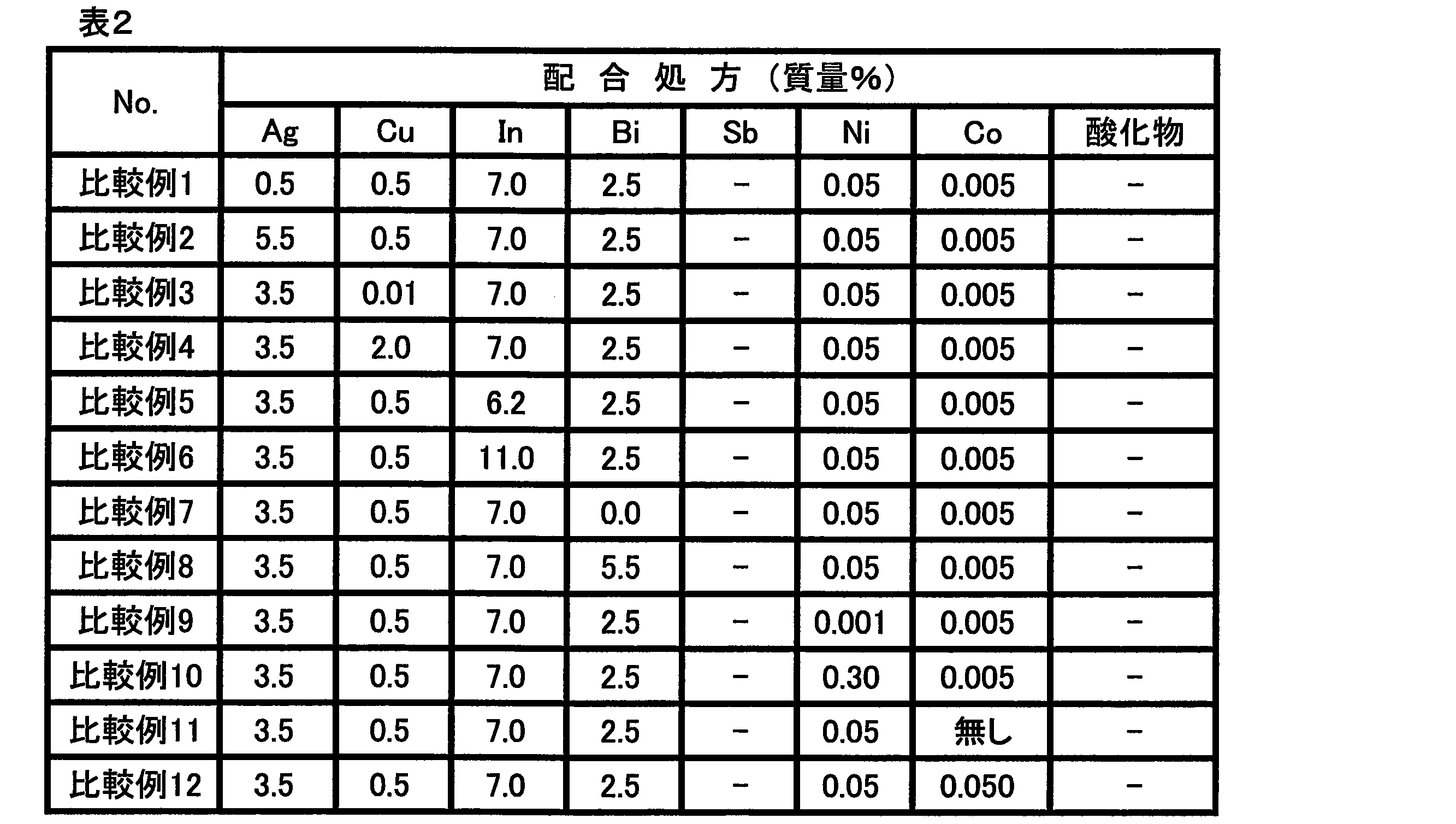
- Examples 1 to 18 and Comparative Examples 1 to 12 -Preparation of solder alloy Each metal, metal oxide and / or metal nitride powder described in Tables 1-2 is mixed in the mixing ratio described in Tables 1-2, and the resulting metal mixture is dissolved in a melting furnace Solder alloys (Examples 1 to 16, Comparative Examples 1 to 12) and solder compositions (Examples 17 to 18) were prepared.
- the mixing ratio of tin (Sn) in the formulation of each example and each comparative example is as follows. Each metal (silver (Ag), copper (Cu), indium (In), bismuth (Bi), This is the balance obtained by subtracting the blending ratio (mass%) of antimony (Sb), nickel (Ni), cobalt (Co)) and the blending ratio (mass%) of metal oxide and / or metal nitride.
- the solder alloy of Example 1 is a mixture of Ag, Cu, In, Bi, Ni, and Co in the proportions shown in Table 1, with the balance being Sn.
- Examples 2 to 4 are examples of prescriptions in which the mixing ratio of Ag is increased or decreased with respect to the prescription of Example 1.
- Examples 5 to 6 are examples of formulations in which the compounding ratio of Cu is increased or decreased with respect to the formulation of Example 1.
- Examples 7 to 8 are examples of prescriptions in which the proportion of In was increased or decreased with respect to the prescription of Example 1.
- Examples 9 to 10 are examples of prescriptions in which the blending ratio of Bi is increased or decreased with respect to the prescription of Example 1.
- Examples 11 to 12 are examples of formulations in which the proportion of Ni was increased or decreased with respect to the formulation of Example 1.
- Examples 13 to 14 are examples of prescriptions in which the blending ratio of Co is increased or decreased with respect to the prescription of Example 1.
- Examples 15 to 16 are examples in which Sb is added to the prescription in Example 1 and the ratio of the Sb is increased or decreased.
- Example 17 is an example of a formulation obtained by further blending zirconium oxide (ZrO 2 ), which is a metal oxide, with the formulation of Example 1 to obtain a solder composition.
- ZrO 2 zirconium oxide
- Example 18 is an example of a formulation obtained by further blending silicon dioxide (SiO 2 ), which is a metal oxide, with the formulation of Example 1 to obtain a solder composition.
- Comparative Examples 1 and 2 are examples of prescriptions in which the proportion of Ag was increased or decreased with respect to the prescription in Example 1 to make Ag excessive or insufficient.
- Comparative Examples 3 to 4 are examples of formulations in which the proportion of Cu was increased or decreased with respect to the formulation of Example 1 to make Cu excessive or insufficient.
- Comparative Examples 5 to 6 are examples of prescriptions in which the proportion of In was increased or decreased with respect to the prescription of Example 1 to make In excessive or insufficient.
- Comparative Examples 7 to 8 are examples of prescriptions in which the mixing ratio of Bi is increased or decreased with respect to the prescription in Example 1 to make Bi excessive or insufficient.
- Comparative Examples 9 to 10 are examples of formulations in which the proportion of Ni was increased or decreased with respect to the formulation of Example 1 to make Ni excessive or insufficient.
- Comparative Examples 11 to 12 are examples of prescriptions in which the proportion of Co was increased or decreased with respect to the prescription in Example 1 to make Co excessive or insufficient.
- solder paste The obtained solder alloy or solder composition is pulverized so as to have a particle size of 25-38 ⁇ m, and the obtained solder alloy powder is mixed with a known flux to obtain a solder paste. Obtained.
- solder paste was printed on a printed circuit board for mounting chip components, and the chip components were mounted by a reflow method.
- the solder paste printing conditions at the time of mounting, the size of the chip component, and the like were appropriately set according to each evaluation described below.
- the sample that had undergone reflow was cut and the cross section was polished. Then, the size of the intermetallic compound structure deposited in the solder after reflow was measured by observing the polished cross section with a scanning electron microscope, and ranked according to the following criteria. The crack resistance is better as the size of the intermetallic compound structure is smaller.
- A The size of the maximum tissue observed was less than 50 ⁇ m.
- B The size of the maximum tissue observed was 50 ⁇ m or more and 100 ⁇ m or less.
- C The size of the maximum tissue observed exceeded 100 ⁇ m.
- ⁇ Erosion resistance (Cu erosion)> The solder alloys obtained in the examples and comparative examples were melted in a solder bath set at 260 ° C. Thereafter, a comb-shaped electrode substrate having copper wiring was immersed in molten solder for 5 seconds. For the comb-shaped electrode substrate having copper wiring, the test substrate “comb-shaped electrode substrate type 2” defined in Appendix 3 “Insulation Resistance Test” of JIS Z 3284-1994 “Solder Paste” was used.
- the operation of immersing the comb substrate in molten solder was repeated, and the number of immersions until the size of the copper wiring of the comb substrate was halved was measured. Considering the reliability of the electronic circuit, the size of the copper wiring must not be halved even if the number of immersions is 4 times or more.
- the case where the number of immersions was 4 times and was not halved was evaluated as “A”, and the case where the number of immersions was halved at 3 times or less was evaluated as “C”.
- ⁇ Durability (Solder life) / Part destruction> The solder paste obtained in each example and each comparative example was printed on a printed circuit board for chip component mounting, and the chip component was mounted by a reflow method.
- the printed film thickness of the solder paste was adjusted using a metal mask having a thickness of 150 ⁇ m.
- a chip component of 3216 size 32 mm ⁇ 16 mm was mounted on a predetermined position of the printed circuit board and heated in a reflow furnace to mount the chip component.
- the reflow conditions were a preheat of 170 to 190 ° C., a peak temperature of 245 ° C. and a time of 220 ° C. or higher for 45 seconds, and a cooling rate when the temperature was lowered from the peak temperature to 200 ° C. was set to 3 to 8 ° C./second.
- the printed circuit board was held for 30 minutes in an environment of ⁇ 40 ° C., and then subjected to a thermal cycle test in which it was held for 30 minutes in an environment of 125 ° C.
- each solder part was cut
- the cross section after polishing was observed with an X-ray photograph to evaluate whether or not a crack generated in the solder fillet portion completely crossed the fillet portion, and was ranked according to the following criteria. The number of evaluation chips in each cycle was 20.
- C Cracks that completely traverse the fillet occurred in less than 1500 cycles.
- solder alloy, the solder composition and the solder paste of the present invention are used in an electronic circuit board used for electric / electronic devices and the like.
Landscapes
- Engineering & Computer Science (AREA)
- Mechanical Engineering (AREA)
- Chemical & Material Sciences (AREA)
- Materials Engineering (AREA)
- Metallurgy (AREA)
- Organic Chemistry (AREA)
- Inorganic Chemistry (AREA)
- Manufacturing & Machinery (AREA)
- Microelectronics & Electronic Packaging (AREA)
- Electric Connection Of Electric Components To Printed Circuits (AREA)
Abstract
Description
・はんだ合金の調製
表1~2に記載の各金属、金属酸化物および/または金属窒化物の粉末を、表1~2に記載の配合割合でそれぞれ混合し、得られた金属混合物を溶解炉にて溶解および均一化させて、はんだ合金(実施例1~16、比較例1~12)およびはんだ組成物(実施例17~18)を調製した。
得られたはんだ合金またははんだ組成物を、粒径が25~38μmとなるように粉末化し、得られたはんだ合金の粉末と、公知のフラックスとを混合して、ソルダペーストを得た。
得られたソルダペーストをチップ部品搭載用のプリント基板に印刷して、リフロー法によりチップ部品を実装した。実装時のソルダペーストの印刷条件、チップ部品のサイズ等については、後述する各評価に応じて適宜設定した。

<耐クラック性(金属間化合物組織の大きさ)>
各実施例および各比較例において得られたソルダペースト0.3gを、厚さ0.3mm、2.5cm四方の銅板の中央部分(約5mm×5mmの領域)に塗布して、こうして得られた試料をリフロー炉で加熱した。リフロー炉による加熱条件は、プリヒートを150~180℃、90秒間とし、ピーク温度を250℃とした。また、220℃以上である時間を120秒間となるように調整し、ピーク温度から200℃まで降温する際の冷却速度を0.5~1.5℃/秒に設定した。なお、このリフロー条件は、一般的なリフローに比べて過酷な条件であって、はんだのスズ中に金属間化合物が析出しやすい条件である。
B:観察される最大組織の大きさが50μm以上100μm以下であった
C:観察される最大組織の大きさが100μmを超えていた
<耐侵食性(Cu喰われ)>
各実施例および比較例において得られたはんだ合金を、260℃に設定されたはんだ槽中で溶融状態にした。その後、銅配線を有するくし形電極基板を溶融はんだ中に5秒間浸漬した。銅配線を有するくし形電極基板には、JIS Z 3284-1994「ソルダペースト」の附属書3「絶縁抵抗試験」に規定の試験基板「くし形電極基板2形」を用いた。
<耐久性(はんだ寿命)・部品破壊>
各実施例および各比較例において得られたソルダペーストを、チップ部品搭載用プリント基板に印刷して、リフロー法によりチップ部品を実装した。ソルダペーストの印刷膜厚は、厚さ150μmのメタルマスクを用いて調整した。ソルダペーストの印刷後、3216サイズ(32mm×16mm)のチップ部品を上記プリント基板の所定位置に搭載して、リフロー炉で加熱し、チップ部品を実装した。リフロー条件は、プリヒートを170~190℃、ピーク温度を245℃、220℃以上である時間が45秒間、ピーク温度から200℃までの降温時の冷却速度を3~8℃/秒に設定した。
A:2500サイクルまでフィレット部を完全に横断する亀裂が発生しなかった。
B:1501~2500サイクルの間でフィレット部を完全に横断する亀裂が発生した。
C:1500サイクル未満でフィレット部を完全に横断する亀裂が発生した。
<総合評価>
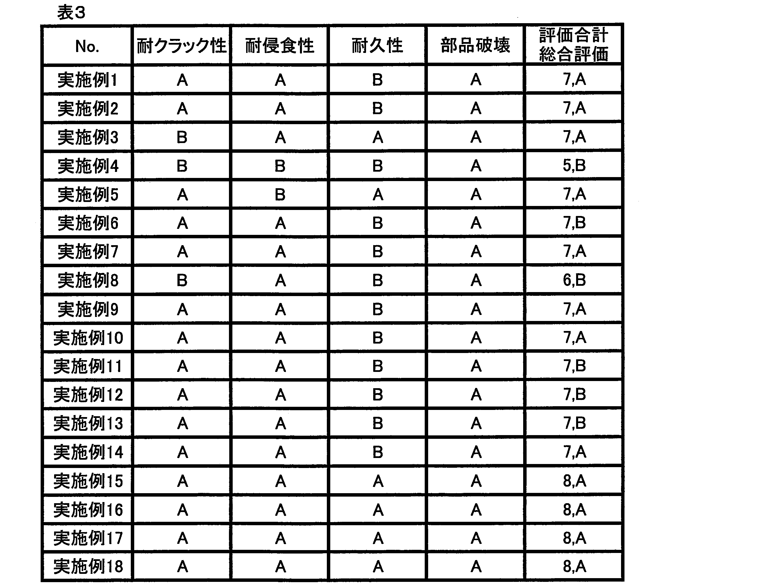
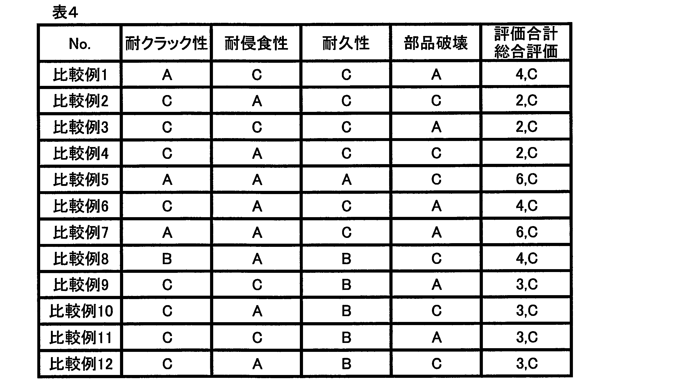
「耐クラック性(はんだ組織の大きさ)」、「耐浸食性(Cu喰われ)」、「耐久性(はんだ寿命)および「部品破壊」の各評価に対する評点として、評価“A”を2点、評価“B”を1点、評価“C”を0点とした。次いで、各評価項目の評点の合計を算出し、評点の合計に基づいて、各実施例および各比較例のソルダペーストを下記の基準によって総合的に評価した。
A:極めて良好(評点合計が7点以上であり、かつ、評価“C”の項目を含まない。)
B:良好(評点合計が5点または6点であり、かつ、評価“C”の項目を含まない。)
C:不良(評点合計が4点以下であるか、または、評価“C”の項目を1つでも含む。)
評価結果を、表3~4に示す。
上述した各実施例および各比較例では、ソルダペーストの評価として、3216サイズ(32mm×16mm)、および、2012サイズ(20mm×12mm)の各種サイズのチップ部品を実装した。
Claims (8)
- スズ-銀-銅系のはんだ合金であって、
実質的に、スズ、銀、銅、ビスマス、ニッケル、コバルトおよびインジウムからなり、
前記はんだ合金の総量に対して、
前記銀の含有割合が、2質量%以上5質量%以下であり、
前記銅の含有割合が、0.1質量%以上1質量%以下であり、
前記ビスマスの含有割合が、0.5質量%以上4.8質量%以下であり、
前記ニッケルの含有割合が、0.01質量%以上0.15質量%以下であり、
前記コバルトの含有割合が、0.001質量%以上0.008質量%以下であり、
前記インジウムの含有割合が、6.2質量%を超過し10質量%以下であり、
前記スズの含有割合が、残余の割合である
ことを特徴とする、はんだ合金。 - さらにアンチモンを含有し、
前記はんだ合金の総量に対して、
前記アンチモンの含有割合が、0.4質量%以上10質量%以下である、請求項1に記載のはんだ合金。 - スズ-銀-銅系のはんだ合金と、金属酸化物および/または金属窒化物とからなるはんだ組成物であって、
前記はんだ合金は、実質的に、スズ、銀、銅、ビスマス、ニッケル、コバルトおよびインジウムからなり、
前記はんだ組成物の総量に対して、
前記銀の含有割合が、2質量%以上5質量%以下であり、
前記銅の含有割合が、0.1質量%以上1質量%以下であり、
前記ビスマスの含有割合が、0.5質量%以上4.8質量%以下であり、
前記ニッケルの含有割合が、0.01質量%以上0.15質量%以下であり、
前記コバルトの含有割合が、0.001質量%以上0.008質量%以下であり、
前記インジウムの含有割合が、6.2質量%を超過し10質量%以下であり、
前記金属酸化物および/または金属窒化物の含有割合が、0質量%を超過し1.0質量%以下であり、
前記スズの含有割合が、残余の割合である
ことを特徴とする、はんだ組成物。 - さらにアンチモンを含有し、
前記はんだ組成物の総量に対して、
前記アンチモンの含有割合が、0.4質量%以上10質量%以下である、請求項3に記載のはんだ組成物。 - はんだ合金からなるはんだ粉末と、
フラックスと
を含有し、
前記はんだ合金は、スズ-銀-銅系のはんだ合金であって、
実質的に、スズ、銀、銅、ビスマス、ニッケル、コバルトおよびインジウムからなり、
前記はんだ合金の総量に対して、
前記銀の含有割合が、2質量%以上5質量%以下であり、
前記銅の含有割合が、0.1質量%以上1質量%以下であり、
前記ビスマスの含有割合が、0.5質量%以上4.8質量%以下であり、
前記ニッケルの含有割合が、0.01質量%以上0.15質量%以下であり、
前記コバルトの含有割合が、0.001質量%以上0.008質量%以下であり、
前記インジウムの含有割合が、6.2質量%を超過し10質量%以下であり、
前記スズの含有割合が、残余の割合である
ことを特徴とする、ソルダペースト。 - はんだ組成物からなるはんだ粉末と、
フラックスと
を含有し、
前記はんだ組成物は、スズ-銀-銅系のはんだ合金と、金属酸化物および/または金属窒化物とからなるはんだ組成物であって、
前記はんだ合金は、実質的に、スズ、銀、銅、ビスマス、ニッケル、コバルトおよびインジウムからなり、
前記はんだ組成物の総量に対して、
前記銀の含有割合が、2質量%以上5質量%以下であり、
前記銅の含有割合が、0.1質量%以上1質量%以下であり、
前記ビスマスの含有割合が、0.5質量%以上4.8質量%以下であり、
前記ニッケルの含有割合が、0.01質量%以上0.15質量%以下であり、
前記コバルトの含有割合が、0.001質量%以上0.008質量%以下であり、
前記インジウムの含有割合が、6.2質量%を超過し10質量%以下であり、
前記金属酸化物および/または金属窒化物の含有割合が、0質量%を超過し1.0質量%以下であり、
前記スズの含有割合が、残余の割合である
ことを特徴とする、ソルダペースト。 - ソルダペーストによるはんだ付部を備え、
前記ソルダペーストは、はんだ合金からなるはんだ粉末と、フラックスとを含有し、
前記はんだ合金は、スズ-銀-銅系のはんだ合金であって、
実質的に、スズ、銀、銅、ビスマス、ニッケル、コバルトおよびインジウムからなり、
前記はんだ合金の総量に対して、
前記銀の含有割合が、2質量%以上5質量%以下であり、
前記銅の含有割合が、0.1質量%以上1質量%以下であり、
前記ビスマスの含有割合が、0.5質量%以上4.8質量%以下であり、
前記ニッケルの含有割合が、0.01質量%以上0.15質量%以下であり、
前記コバルトの含有割合が、0.001質量%以上0.008質量%以下であり、
前記インジウムの含有割合が、6.2質量%を超過し10質量%以下であり、
前記スズの含有割合が、残余の割合である
ことを特徴とする、電子回路基板。 - ソルダペーストによるはんだ付部を備え、
前記ソルダペーストは、はんだ組成物からなるはんだ粉末と、フラックスとを含有し、
前記はんだ組成物は、スズ-銀-銅系のはんだ合金と、金属酸化物および/または金属窒化物とからなるはんだ組成物であって、
前記はんだ合金は、実質的に、スズ、銀、銅、ビスマス、ニッケル、コバルトおよびインジウムからなり、
前記はんだ組成物の総量に対して、
前記銀の含有割合が、2質量%以上5質量%以下であり、
前記銅の含有割合が、0.1質量%以上1質量%以下であり、
前記ビスマスの含有割合が、0.5質量%以上4.8質量%以下であり、
前記ニッケルの含有割合が、0.01質量%以上0.15質量%以下であり、
前記コバルトの含有割合が、0.001質量%以上0.008質量%以下であり、
前記インジウムの含有割合が、6.2質量%を超過し10質量%以下であり、
前記金属酸化物および/または金属窒化物の含有割合が、0質量%を超過し1.0質量%以下であり、
前記スズの含有割合が、残余の割合である
ことを特徴とする、電子回路基板。
Priority Applications (5)
| Application Number | Priority Date | Filing Date | Title |
|---|---|---|---|
| EP14863041.1A EP2979807B1 (en) | 2014-06-24 | 2014-08-28 | Solder alloy, solder composition, solder paste and electronic circuit board |
| CN201480003527.8A CN105431253A (zh) | 2014-06-24 | 2014-08-28 | 焊料合金、焊料组合物、钎焊膏以及电子线路基板 |
| CA2892424A CA2892424C (en) | 2014-06-24 | 2014-08-28 | Solder alloy, solder composition, solder paste, and electronic circuit board |
| JP2014542600A JP5638174B1 (ja) | 2014-06-24 | 2014-08-28 | はんだ合金、はんだ組成物、ソルダペーストおよび電子回路基板 |
| US14/442,628 US9931716B2 (en) | 2014-06-24 | 2014-08-28 | Solder alloy, solder composition, solder paste, and electronic circuit board |
Applications Claiming Priority (2)
| Application Number | Priority Date | Filing Date | Title |
|---|---|---|---|
| JP2014-129472 | 2014-06-24 | ||
| JP2014129472 | 2014-06-24 |
Publications (1)
| Publication Number | Publication Date |
|---|---|
| WO2015198496A1 true WO2015198496A1 (ja) | 2015-12-30 |
Family
ID=54344647
Family Applications (2)
| Application Number | Title | Priority Date | Filing Date |
|---|---|---|---|
| PCT/JP2014/072576 Ceased WO2015198497A1 (ja) | 2014-06-24 | 2014-08-28 | はんだ合金、ソルダペーストおよび電子回路基板 |
| PCT/JP2014/072575 Ceased WO2015198496A1 (ja) | 2014-06-24 | 2014-08-28 | はんだ合金、はんだ組成物、ソルダペーストおよび電子回路基板 |
Family Applications Before (1)
| Application Number | Title | Priority Date | Filing Date |
|---|---|---|---|
| PCT/JP2014/072576 Ceased WO2015198497A1 (ja) | 2014-06-24 | 2014-08-28 | はんだ合金、ソルダペーストおよび電子回路基板 |
Country Status (10)
| Country | Link |
|---|---|
| US (2) | US9931716B2 (ja) |
| EP (2) | EP3093098B1 (ja) |
| JP (1) | JP5638174B1 (ja) |
| KR (2) | KR101551613B1 (ja) |
| CN (2) | CN105377503B (ja) |
| CA (1) | CA2892424C (ja) |
| ES (1) | ES2710219T3 (ja) |
| MY (2) | MY162879A (ja) |
| TW (2) | TWI535855B (ja) |
| WO (2) | WO2015198497A1 (ja) |
Cited By (1)
| Publication number | Priority date | Publication date | Assignee | Title |
|---|---|---|---|---|
| JP7161133B1 (ja) | 2021-09-30 | 2022-10-26 | 千住金属工業株式会社 | はんだ合金、はんだボール、はんだプリフォーム、はんだペースト及びはんだ継手 |
Families Citing this family (23)
| Publication number | Priority date | Publication date | Assignee | Title |
|---|---|---|---|---|
| WO2016012754A2 (en) * | 2014-07-21 | 2016-01-28 | Alpha Metals, Inc. | Low temperature high reliability alloy for solder hierarchy |
| JP5723056B1 (ja) * | 2014-12-15 | 2015-05-27 | ハリマ化成株式会社 | はんだ合金、ソルダペーストおよび電子回路基板 |
| CN105665956A (zh) * | 2016-03-23 | 2016-06-15 | 徐宏达 | 一种用于钎焊铝及其合金的软钎料合金 |
| JP2017213596A (ja) * | 2016-06-02 | 2017-12-07 | パナソニックIpマネジメント株式会社 | はんだ合金およびそれを用いた実装構造体 |
| JP6365653B2 (ja) * | 2016-08-19 | 2018-08-01 | 千住金属工業株式会社 | はんだ合金、はんだ継手およびはんだ付け方法 |
| CN106835214A (zh) * | 2016-12-27 | 2017-06-13 | 浙江亚通焊材有限公司 | 一种Sn‑Bi系无铅低温焊料的电沉积方法 |
| DE102017107715B4 (de) * | 2017-04-10 | 2022-03-03 | Infineon Technologies Ag | Magnetisches Sensor-Package und Verfahren zur Herstellung eines magnetischen Sensor-Packages |
| KR102286739B1 (ko) * | 2017-08-17 | 2021-08-05 | 현대자동차 주식회사 | 무연 솔더 조성물 |
| CN111344106B (zh) * | 2017-11-24 | 2022-03-04 | 千住金属工业株式会社 | 软钎料材料、焊膏和钎焊接头 |
| JP6578393B2 (ja) * | 2018-02-27 | 2019-09-18 | 株式会社タムラ製作所 | 鉛フリーはんだ合金、電子回路実装基板及び電子制御装置 |
| JP6540869B1 (ja) * | 2018-03-30 | 2019-07-10 | 千住金属工業株式会社 | はんだペースト |
| JP6521161B1 (ja) * | 2018-07-20 | 2019-05-29 | 千住金属工業株式会社 | はんだ合金、はんだ粉末、はんだペースト、およびこれらを用いたはんだ継手 |
| JP6521160B1 (ja) * | 2018-07-20 | 2019-05-29 | 千住金属工業株式会社 | はんだ合金、はんだ粉末、はんだペースト、およびこれらを用いたはんだ継手 |
| WO2020047481A1 (en) * | 2018-08-31 | 2020-03-05 | Indium Corporation | Snbi and snin solder alloys |
| KR20240042569A (ko) * | 2018-10-24 | 2024-04-02 | 알파 어셈블리 솔루션스 인크. | 중합체 기재, 인쇄 회로 기판 및 기타 접합 응용을 위한 저온 납땜 해법 |
| JP6573019B1 (ja) | 2018-10-25 | 2019-09-11 | 千住金属工業株式会社 | フラックス及びソルダペースト |
| JP6649596B1 (ja) * | 2019-05-27 | 2020-02-19 | 千住金属工業株式会社 | はんだ合金、はんだ粉末、およびはんだ継手 |
| JP6708942B1 (ja) * | 2019-05-27 | 2020-06-10 | 千住金属工業株式会社 | はんだ合金、はんだペースト、プリフォームはんだ、はんだボール、線はんだ、脂入りはんだ、はんだ継手、電子回路基板および多層電子回路基板 |
| WO2020241319A1 (ja) | 2019-05-27 | 2020-12-03 | 千住金属工業株式会社 | はんだ合金、ソルダペースト、はんだボール、ソルダプリフォーム、およびはんだ継手 |
| US11383330B2 (en) | 2020-09-21 | 2022-07-12 | Aptiv Technologies Limited | Lead-free solder composition |
| CN112643240A (zh) * | 2020-12-10 | 2021-04-13 | 东莞市清大菁玉科技有限公司 | 一种应用于高频数据线线焊接的新型低温高导电率钎料及其制备方法 |
| TWI882827B (zh) * | 2024-06-05 | 2025-05-01 | 大瑞科技股份有限公司 | 錫基合金及錫球 |
| TWI911104B (zh) * | 2025-04-24 | 2026-01-01 | 大瑞科技股份有限公司 | 錫基合金、錫球、焊點 |
Citations (5)
| Publication number | Priority date | Publication date | Assignee | Title |
|---|---|---|---|---|
| JP2008521619A (ja) * | 2004-12-01 | 2008-06-26 | アルファ フライ リミテッド | はんだ合金 |
| WO2009011392A1 (ja) * | 2007-07-18 | 2009-01-22 | Senju Metal Industry Co., Ltd. | 車載電子回路用In入り鉛フリーはんだ |
| JP2012106280A (ja) * | 2010-10-29 | 2012-06-07 | Harima Chemicals Inc | 低銀はんだ合金およびはんだペースト組成物 |
| JP2013193092A (ja) * | 2012-03-16 | 2013-09-30 | Panasonic Corp | はんだ材料および実装体 |
| JP5349703B1 (ja) | 2012-07-19 | 2013-11-20 | ハリマ化成株式会社 | はんだ合金、ソルダペーストおよび電子回路基板 |
Family Cites Families (30)
| Publication number | Priority date | Publication date | Assignee | Title |
|---|---|---|---|---|
| JPH0825050B2 (ja) | 1993-06-08 | 1996-03-13 | 日本アルミット株式会社 | 無含鉛半田合金 |
| JPH0970687A (ja) | 1995-07-04 | 1997-03-18 | Toyota Central Res & Dev Lab Inc | 無鉛はんだ合金 |
| US6224690B1 (en) * | 1995-12-22 | 2001-05-01 | International Business Machines Corporation | Flip-Chip interconnections using lead-free solders |
| WO1998048069A1 (en) | 1997-04-22 | 1998-10-29 | Ecosolder International Pty Limited | Lead-free solder |
| DE19729545A1 (de) | 1997-07-10 | 1999-01-14 | Euromat Gmbh | Lotlegierung |
| US6176947B1 (en) | 1998-12-31 | 2001-01-23 | H-Technologies Group, Incorporated | Lead-free solders |
| JP2002096191A (ja) | 2000-09-18 | 2002-04-02 | Matsushita Electric Ind Co Ltd | はんだ材料およびこれを利用する電気・電子機器 |
| HU228577B1 (en) * | 2000-11-16 | 2013-04-29 | Singapore Asahi Chemical And Solder Ind Pte Ltd | Lead-free solders |
| JP2003126987A (ja) | 2001-10-16 | 2003-05-08 | Denki Kagaku Kogyo Kk | 回路基板用鉛フリー半田及び回路基板 |
| JP2003275892A (ja) * | 2002-03-20 | 2003-09-30 | Tamura Kaken Co Ltd | 無鉛はんだ合金及びソルダペースト組成物 |
| JP2004188453A (ja) | 2002-12-11 | 2004-07-08 | Harima Chem Inc | Sn系はんだ合金 |
| KR101059710B1 (ko) * | 2003-04-01 | 2011-08-29 | 파나소닉 주식회사 | 솔더 페이스트 및 인쇄 회로 기판 |
| EP1889684B1 (en) | 2005-06-03 | 2016-03-30 | Senju Metal Industry Co., Ltd. | Lead-free solder alloy |
| JP2007196289A (ja) | 2005-12-27 | 2007-08-09 | Toshiba Corp | 電子部品用無鉛金属材料 |
| WO2008004531A2 (en) | 2006-07-05 | 2008-01-10 | Fuji Electric Holdings Co., Ltd. | Cream solder and method of soldering electronic part |
| DE102006047764A1 (de) | 2006-10-06 | 2008-04-10 | W.C. Heraeus Gmbh | Bleifreies Weichlot mit verbesserten Eigenschaften bei Temperaturen >150°C |
| JP2008168322A (ja) * | 2007-01-11 | 2008-07-24 | Ishikawa Kinzoku Kk | Fe浸食抑制鉛フリーはんだ合金 |
| WO2009011341A1 (ja) | 2007-07-13 | 2009-01-22 | Senju Metal Industry Co., Ltd. | 車載実装用鉛フリーはんだと車載電子回路 |
| CN101537545A (zh) * | 2008-03-21 | 2009-09-23 | 喜星素材株式会社 | 低温焊接焊用无铅合金 |
| US8598464B2 (en) | 2009-04-20 | 2013-12-03 | Panasonic Corporation | Soldering material and electronic component assembly |
| CN102172805B (zh) * | 2011-01-18 | 2013-01-02 | 哈尔滨理工大学 | 一种电子封装用低成本抗老化钎料及其制备方法 |
| KR101752616B1 (ko) | 2011-02-25 | 2017-06-29 | 센주긴조쿠고교 가부시키가이샤 | 파워 디바이스용의 땜납 합금과 고전류 밀도의 땜납 조인트 |
| WO2012127642A1 (ja) | 2011-03-23 | 2012-09-27 | 千住金属工業株式会社 | 鉛フリーはんだ合金 |
| JP2014527466A (ja) | 2011-08-02 | 2014-10-16 | アルファ・メタルズ・インコーポレイテッドAlpha Metals,Inc. | はんだ組成物 |
| JP2013252548A (ja) * | 2012-06-08 | 2013-12-19 | Nihon Almit Co Ltd | 微細部品接合用のソルダペースト |
| JP5238088B1 (ja) | 2012-06-29 | 2013-07-17 | ハリマ化成株式会社 | はんだ合金、ソルダペーストおよび電子回路基板 |
| WO2014002304A1 (ja) * | 2012-06-29 | 2014-01-03 | ハリマ化成株式会社 | はんだ合金、ソルダペーストおよび電子回路基板 |
| KR101639220B1 (ko) | 2012-12-18 | 2016-07-13 | 센주긴조쿠고교 가부시키가이샤 | 납 프리 땜납 합금 |
| CN103203563A (zh) * | 2013-04-08 | 2013-07-17 | 上海大学 | 纳米TiO2颗粒强化复合无铅焊料 |
| CN103341699A (zh) | 2013-07-04 | 2013-10-09 | 浙江亚通焊材有限公司 | 一种取代锡铅钎料的Sn-In-Ag无铅钎料 |
-
2014
- 2014-08-28 WO PCT/JP2014/072576 patent/WO2015198497A1/ja not_active Ceased
- 2014-08-28 MY MYPI2015001202A patent/MY162879A/en unknown
- 2014-08-28 EP EP14853188.2A patent/EP3093098B1/en active Active
- 2014-08-28 CN CN201480003546.0A patent/CN105377503B/zh active Active
- 2014-08-28 KR KR1020157013420A patent/KR101551613B1/ko active Active
- 2014-08-28 JP JP2014542600A patent/JP5638174B1/ja active Active
- 2014-08-28 WO PCT/JP2014/072575 patent/WO2015198496A1/ja not_active Ceased
- 2014-08-28 CN CN201480003527.8A patent/CN105431253A/zh active Pending
- 2014-08-28 MY MYPI2015001375A patent/MY162428A/en unknown
- 2014-08-28 US US14/442,628 patent/US9931716B2/en active Active
- 2014-08-28 EP EP14863041.1A patent/EP2979807B1/en active Active
- 2014-08-28 US US14/442,597 patent/US9956649B2/en active Active
- 2014-08-28 CA CA2892424A patent/CA2892424C/en active Active
- 2014-08-28 KR KR1020157013423A patent/KR101551614B1/ko active Active
- 2014-08-28 ES ES14853188T patent/ES2710219T3/es active Active
- 2014-09-29 TW TW103133721A patent/TWI535855B/zh active
- 2014-09-29 TW TW103133722A patent/TWI558491B/zh active
Patent Citations (6)
| Publication number | Priority date | Publication date | Assignee | Title |
|---|---|---|---|---|
| JP2008521619A (ja) * | 2004-12-01 | 2008-06-26 | アルファ フライ リミテッド | はんだ合金 |
| WO2009011392A1 (ja) * | 2007-07-18 | 2009-01-22 | Senju Metal Industry Co., Ltd. | 車載電子回路用In入り鉛フリーはんだ |
| JP2012106280A (ja) * | 2010-10-29 | 2012-06-07 | Harima Chemicals Inc | 低銀はんだ合金およびはんだペースト組成物 |
| JP2013193092A (ja) * | 2012-03-16 | 2013-09-30 | Panasonic Corp | はんだ材料および実装体 |
| JP5349703B1 (ja) | 2012-07-19 | 2013-11-20 | ハリマ化成株式会社 | はんだ合金、ソルダペーストおよび電子回路基板 |
| WO2014013632A1 (ja) * | 2012-07-19 | 2014-01-23 | ハリマ化成株式会社 | はんだ合金、ソルダペーストおよび電子回路基板 |
Non-Patent Citations (1)
| Title |
|---|
| See also references of EP2979807A4 |
Cited By (3)
| Publication number | Priority date | Publication date | Assignee | Title |
|---|---|---|---|---|
| JP7161133B1 (ja) | 2021-09-30 | 2022-10-26 | 千住金属工業株式会社 | はんだ合金、はんだボール、はんだプリフォーム、はんだペースト及びはんだ継手 |
| WO2023054629A1 (ja) * | 2021-09-30 | 2023-04-06 | 千住金属工業株式会社 | はんだ合金、はんだボール、はんだプリフォーム、はんだペースト及びはんだ継手 |
| JP2023051074A (ja) * | 2021-09-30 | 2023-04-11 | 千住金属工業株式会社 | はんだ合金、はんだボール、はんだプリフォーム、はんだペースト及びはんだ継手 |
Also Published As
| Publication number | Publication date |
|---|---|
| CN105377503B (zh) | 2016-10-12 |
| CN105377503A (zh) | 2016-03-02 |
| US9931716B2 (en) | 2018-04-03 |
| EP3093098A1 (en) | 2016-11-16 |
| CA2892424C (en) | 2016-08-09 |
| US20160271737A1 (en) | 2016-09-22 |
| MY162879A (en) | 2017-07-20 |
| TW201600610A (zh) | 2016-01-01 |
| TWI558491B (zh) | 2016-11-21 |
| JPWO2015198496A1 (ja) | 2017-04-20 |
| CA2892424A1 (en) | 2015-11-24 |
| TWI535855B (zh) | 2016-06-01 |
| US9956649B2 (en) | 2018-05-01 |
| EP2979807A4 (en) | 2016-12-07 |
| KR101551614B1 (ko) | 2015-09-08 |
| EP3093098B1 (en) | 2019-01-02 |
| JP5638174B1 (ja) | 2014-12-10 |
| KR101551613B1 (ko) | 2015-09-08 |
| EP3093098A4 (en) | 2017-12-13 |
| TW201600216A (zh) | 2016-01-01 |
| MY162428A (en) | 2017-06-15 |
| WO2015198497A1 (ja) | 2015-12-30 |
| CN105431253A (zh) | 2016-03-23 |
| ES2710219T3 (es) | 2019-04-23 |
| US20160288271A1 (en) | 2016-10-06 |
| EP2979807A1 (en) | 2016-02-03 |
| EP2979807B1 (en) | 2018-04-11 |
Similar Documents
| Publication | Publication Date | Title |
|---|---|---|
| JP5638174B1 (ja) | はんだ合金、はんだ組成物、ソルダペーストおよび電子回路基板 | |
| JP5349703B1 (ja) | はんだ合金、ソルダペーストおよび電子回路基板 | |
| JP5730354B2 (ja) | はんだ組成物、ソルダペーストおよび電子回路基板 | |
| JP5730353B2 (ja) | はんだ組成物、ソルダペーストおよび電子回路基板 | |
| JP6053248B1 (ja) | はんだ合金、ソルダペーストおよび電子回路基板 | |
| JP5238088B1 (ja) | はんだ合金、ソルダペーストおよび電子回路基板 | |
| TWI508812B (zh) | Solder alloy, solder paste and electronic circuit substrate | |
| JP5654716B1 (ja) | はんだ合金、ソルダペーストおよび電子回路基板 |
Legal Events
| Date | Code | Title | Description |
|---|---|---|---|
| WWE | Wipo information: entry into national phase |
Ref document number: 201480003527.8 Country of ref document: CN |
|
| ENP | Entry into the national phase |
Ref document number: 2014542600 Country of ref document: JP Kind code of ref document: A |
|
| WWE | Wipo information: entry into national phase |
Ref document number: 14442628 Country of ref document: US |
|
| WWE | Wipo information: entry into national phase |
Ref document number: 2892424 Country of ref document: CA |
|
| WWE | Wipo information: entry into national phase |
Ref document number: 1020157013420 Country of ref document: KR |
|
| WWE | Wipo information: entry into national phase |
Ref document number: 2014863041 Country of ref document: EP |
|
| NENP | Non-entry into the national phase |
Ref country code: DE |