WO2015198833A1 - Dispositif de protection contre les décharges électrostatiques et son procédé de fabrication - Google Patents
Dispositif de protection contre les décharges électrostatiques et son procédé de fabrication Download PDFInfo
- Publication number
- WO2015198833A1 WO2015198833A1 PCT/JP2015/066298 JP2015066298W WO2015198833A1 WO 2015198833 A1 WO2015198833 A1 WO 2015198833A1 JP 2015066298 W JP2015066298 W JP 2015066298W WO 2015198833 A1 WO2015198833 A1 WO 2015198833A1
- Authority
- WO
- WIPO (PCT)
- Prior art keywords
- discharge
- particles
- electrode
- protection device
- auxiliary electrode
- Prior art date
- Legal status (The legal status is an assumption and is not a legal conclusion. Google has not performed a legal analysis and makes no representation as to the accuracy of the status listed.)
- Ceased
Links
Images




Classifications
-
- H—ELECTRICITY
- H02—GENERATION; CONVERSION OR DISTRIBUTION OF ELECTRIC POWER
- H02H—EMERGENCY PROTECTIVE CIRCUIT ARRANGEMENTS
- H02H9/00—Emergency protective circuit arrangements for limiting excess current or voltage without disconnection
- H02H9/04—Emergency protective circuit arrangements for limiting excess current or voltage without disconnection responsive to excess voltage
- H02H9/044—Physical layout, materials not provided for elsewhere
-
- H—ELECTRICITY
- H01—ELECTRIC ELEMENTS
- H01T—SPARK GAPS; OVERVOLTAGE ARRESTERS USING SPARK GAPS; SPARKING PLUGS; CORONA DEVICES; GENERATING IONS TO BE INTRODUCED INTO NON-ENCLOSED GASES
- H01T4/00—Overvoltage arresters using spark gaps
- H01T4/10—Overvoltage arresters using spark gaps having a single gap or a plurality of gaps in parallel
- H01T4/12—Overvoltage arresters using spark gaps having a single gap or a plurality of gaps in parallel hermetically sealed
-
- H—ELECTRICITY
- H01—ELECTRIC ELEMENTS
- H01T—SPARK GAPS; OVERVOLTAGE ARRESTERS USING SPARK GAPS; SPARKING PLUGS; CORONA DEVICES; GENERATING IONS TO BE INTRODUCED INTO NON-ENCLOSED GASES
- H01T1/00—Details of spark gaps
- H01T1/20—Means for starting arc or facilitating ignition of spark gap
Definitions
- the present invention relates to an electrostatic discharge protection device that protects electronic equipment from destruction due to electrostatic discharge and a method for manufacturing the same.
- Electrostatic discharge protection devices are widely used to prevent electronic devices from being destroyed or malfunctioning due to electrostatic discharge (ESD).
- Patent Document 1 has a ceramic multilayer substrate, a cavity formed inside the ceramic multilayer substrate, and a facing portion arranged so that the tips are opposed to each other with a space in the cavity.
- An ESD protection device having at least one pair of discharge electrodes and an external electrode formed on the surface of the ceramic multilayer substrate and connected to the discharge electrodes is disclosed.
- the ceramic multilayer substrate is in the vicinity of the surface provided with the discharge electrode, and is disposed adjacent to at least the facing portion of the discharge electrode and the portion between the facing portions.
- a ceramic material has a metal material content of 10 vol% or more and 50 vol% or less. Since the ESD protection device described in Patent Document 1 has the above-described configuration, the discharge start voltage can be accurately set.
- the first and second discharge electrodes disposed so as to face each other, the discharge auxiliary electrode formed so as to straddle between the first and second discharge electrodes, and the first and second An ESD protection device comprising a discharge electrode and an insulating base material holding a discharge auxiliary electrode is disclosed.
- the discharge auxiliary electrode includes a core-shell including a core portion mainly composed of a first metal and a shell portion mainly composed of a metal oxide including a second metal. It is comprised from the aggregate
- Patent Document 3 discloses an overvoltage that is connected between a first electrode, a second electrode, a first electrode, and a second electrode, and includes a nonconductive powder, a metal conductive powder, and an adhesive.
- An overvoltage protection element is disclosed that includes a porous structure produced by firing using a material for the protection element. In the manufacture of the overvoltage protection element described in Patent Document 3, by using the material of the above-described overvoltage protection element, breakdown due to discharge energy can be suppressed, and the service life of the element can be extended.
- the ESD protection device In recent years, with the improvement in performance of electronic devices, it is required to further lower the discharge start voltage of the ESD protection device in order to more reliably prevent the destruction and malfunction of the electronic device due to electrostatic discharge. On the other hand, in a normal use state, the ESD protection device is required to have a sufficiently high insulating property (initial insulating property) in order to suppress the occurrence of a short circuit defect. In addition, there is a need to develop an ESD protection device that can suppress a decrease in insulation even when ESD is repeatedly applied and has excellent repeated resistance.
- An object of the present invention is to provide an electrostatic discharge protection device having good initial insulation and repeated resistance and having a good operation rate at a relatively low discharge voltage of 2 kV.
- the present inventors have made researches by paying attention to the composition of the discharge auxiliary electrode existing between two discharge electrodes arranged opposite to each other and spaced apart from each other.
- the present inventors used a discharge auxiliary electrode including semiconductor particles and metal particles having an oxygen-containing layer on the surface, and the average particle diameter and density of the metal particles in the discharge auxiliary electrode were within a specific numerical range.
- the present invention has been completed.
- an insulating substrate A first discharge electrode and a second discharge electrode arranged to contact the insulating substrate, wherein the first and second discharge electrodes are arranged opposite to each other and spaced apart from each other; First and second external electrodes provided on the outer surface of the insulating substrate, the first external electrode being electrically connected to the first discharge electrode, and the second external electrode being a second discharge An external electrode electrically connected to the electrode;
- An electrostatic discharge protection device comprising a discharge auxiliary electrode that exists across the first discharge electrode and the second discharge electrode in a region where the first and second discharge electrodes face each other,
- the discharge auxiliary electrode includes at least semiconductor particles and metal particles, The average particle size of the metal particles is 0.3 to 1.5 ⁇ m, The existence density of metal particles in an arbitrary cross section of the discharge auxiliary electrode is 20 particles / 50 ⁇ m 2 or more,
- the semiconductor particle is provided with an electrostatic discharge protection device having an oxygen-containing layer on a surface thereof.
- the second aspect of the present invention (a) semiconductor particles having metal particles on one main surface of the first ceramic green sheet and an oxygen-containing layer on the surface, the oxygen in the semiconductor particles A step of forming an unfired discharge auxiliary electrode by applying a discharge auxiliary electrode paste containing semiconductor particles having a content of 1.0 to 7.0% by weight and an organic vehicle, the average of metal particles A process in which the particle size is 0.10 to 1.00 ⁇ m, and the volume fraction of the metal particles is 15 to 40% by volume with respect to the whole non-combustible component including the metal particles and the semiconductor particles; (B) forming the first and second unsintered discharge electrodes by applying the discharge electrode paste on the first ceramic green sheet to which the discharge auxiliary electrode paste is applied, And the second unsintered discharge electrode, each of which is disposed at least partially on the unsintered discharge auxiliary electrode and disposed opposite to and spaced apart from each other on the unsintered discharge assist electrode.
- the second ceramic green sheet is laminated on the first ceramic green sheet to which the discharge auxiliary electrode paste, the discharge electrode paste, and the cavity forming paste are applied, and molded to a predetermined size.
- an electrostatic discharge protection device which includes a step of forming first and second external electrodes by subjecting to a baking process.
- the electrostatic discharge protection device according to the present invention Since the electrostatic discharge protection device according to the present invention has the above-described configuration, it has good initial insulation and a good operation rate at a relatively low discharge voltage of 2 kV.
- the method for manufacturing an electrostatic discharge protection device according to the present invention has the above-described configuration, so that it has good initial insulation and repeated resistance, and has a good operation rate at a relatively low discharge voltage of 2 kV.
- a discharge protection device can be provided.
- FIG. 1 is a schematic cross-sectional view showing a configuration of an ESD protection device according to the first embodiment of the present invention.
- FIG. 2 (a) is a scanning electron microscope (SEM) image of the discharge auxiliary electrode before ESD application
- FIG. 2 (b) is a discharge auxiliary electrode SEM image after ESD application
- FIG. It is a schematic diagram of the semiconductor particle sintered by ESD application.
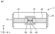
- FIG. 3 is a schematic plan view showing the arrangement of discharge electrodes in the ESD protection device according to the first embodiment.
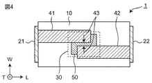
- FIG. 4 is a schematic plan view showing a first modification of the arrangement of the discharge electrodes in the ESD protection device according to the first embodiment.
- FIG. 1 is a schematic cross-sectional view showing a configuration of an ESD protection device according to the first embodiment of the present invention.
- FIG. 2 (a) is a scanning electron microscope (SEM) image of the discharge auxiliary electrode before ESD application
- FIG. 2 (b) is a discharge auxiliary electrode SEM image after ESD
- FIG. 5 is a schematic cross-sectional view showing a second modification of the arrangement of discharge electrodes in the ESD protection device according to the first embodiment.
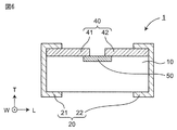
- FIG. 6 is a schematic cross-sectional view showing a configuration of an ESD protection device according to the second embodiment of the present invention.
- FIG. 7 is a schematic cross-sectional view showing a first modification of the configuration of the ESD protection device according to the second embodiment of the present invention.
- FIG. 8 is a schematic cross-sectional view showing a second modification of the configuration of the ESD protection device according to the second embodiment of the present invention.
- FIG. 9 is a schematic cross-sectional view showing a third modification of the configuration of the ESD protection device according to the second embodiment of the present invention.
- FIG. 1 is a schematic cross-sectional view showing the configuration of an electrostatic discharge (ESD) protection device 1 according to an embodiment of the present invention.
- An ESD protection device 1 shown in FIG. 1 includes an insulating substrate 10, a first discharge electrode 41 and a second discharge electrode 42 (collectively referred to as a discharge electrode 40) arranged so as to be in contact with the insulating substrate 10.
- the first external electrode 21 and the second external electrode 22 (sometimes collectively referred to as the external electrode 20) provided on the outer surface of the insulating substrate 10, and the first discharge electrode 41 In the region where the first discharge electrode 42 and the second discharge electrode 42 face each other, the first discharge electrode 41 and the auxiliary discharge electrode 50 existing across the second discharge electrode 42 are included.
- the mechanism capable of achieving good initial insulation and good operating rate at a relatively low discharge voltage is not bound by any theory. It is thought that it is as follows.
- a relatively low discharge voltage eg 2 kV
- the discharge auxiliary electrode 50 has a function of promoting creeping discharge.
- the discharge start voltage due to creeping discharge tends to be lower than the discharge start voltage due to air discharge. Therefore, by providing the auxiliary discharge electrode 50, the discharge start voltage can be lowered.
- the discharge auxiliary electrode has insulating properties as a whole by including semiconductor particles in addition to metal particles. Therefore, it is possible to suppress the occurrence of a short circuit due to contact between the metal particles, and it is possible to achieve good initial insulation.
- the smaller the metal particles in the discharge auxiliary electrode the more easily the electric field is concentrated between the end of the discharge electrode and the metal particles in the discharge auxiliary electrode, and the electric field generated tends to increase. Since the metal particles contained in the discharge auxiliary electrode in the present invention are fine particles having an average particle diameter of 0.3 to 1.5 ⁇ m, the generated electric field can be increased. In addition, the larger the amount of metal particles contained in the discharge auxiliary electrode, the more points (electric field points) where an electric field is generated.
- the discharge auxiliary electrode according to the present invention has a density of metal particles in an arbitrary cross section of 20 particles / 50 ⁇ m 2 or more, and includes a large number of metal particles, so that a large number of electric field points can be generated.
- a leader streamer (electronic avalanche) can occur at the end of one discharge electrode (for example, the first discharge electrode) due to the above-described electric field concentration. Since the discharge auxiliary electrode in the present invention contains a large number of metal particles, a large amount of leader streamer can be generated, and the other discharge electrode (for example, the second discharge electrode) can be generated without stalling the leader streamer. Can be advanced. As a result, the ESD protection device according to the present invention can effectively generate the creeping discharge between the discharge electrodes, so that a good operation rate at a relatively low discharge voltage (for example, 2 kV) can be achieved.
- a relatively low discharge voltage for example, 2 kV
- the gas present in the region between the discharge electrodes is a gas that is easily ionized, such as a rare gas, ionization of gas molecules is likely to occur, and a large amount of gas ions can be generated. As a result, creeping discharge between the discharge electrodes can be generated more effectively, and the operation rate at a relatively low discharge voltage (for example, 2 kV) can be further improved.
- FIG. 2A is a scanning electron microscope (SEM) image of the discharge auxiliary electrode before ESD application
- FIG. 2B is an SEM image of the discharge auxiliary electrode after ESD application.
- the discharge auxiliary electrode includes metal particles 51 and semiconductor particles 71. 2 (a) and 2 (b), it can be seen that when ESD is applied, the semiconductor particles 71 are sintered into a lump. When the semiconductor particles 71 are sintered, a grain boundary layer having a high resistance value is formed between the semiconductor particles 71.
- FIG. 2C schematically shows semiconductor particles 71 sintered by applying ESD to form a varistor structure.
- the conductivity of the varistor structure depends on the thickness of the insulating layer present at the grain boundary of the semiconductor particles 71. When the thickness of the insulating layer present at the semiconductor grain boundary is thin, the conductivity of the varistor structure is high. Therefore, if the semiconductor particles 71 in the discharge auxiliary electrode form a varistor structure by applying ESD, the resistance value of the discharge auxiliary electrode may be lowered.
- the semiconductor particles 71 present in the discharge auxiliary electrode have an insulating oxygen-containing layer 72 on the surface thereof. Therefore, even when the semiconductor particles 71 are sintered by the heat generated due to the application of ESD, an insulating layer can be effectively present at the grain boundaries of the semiconductor particles 71, thereby A decrease in insulation after application can be suppressed.
- FIG. 1 is a schematic cross-sectional view of an electrostatic discharge protection device (ESD protection device) according to the first embodiment of the present invention.
- the ESD protection device 1 shown in FIG. 1 includes an insulating substrate 10, a first discharge electrode 41 and a second discharge electrode 42 arranged so as to be in contact with the insulating substrate 10, and an insulating substrate 10. In the region where the first external electrode 21 and the second external electrode 22 provided on the outer surface, and the first discharge electrode 41 and the second discharge electrode 42 face each other, the first discharge electrode 41 and And a discharge auxiliary electrode 50 existing across the second discharge electrode 42.
- the ESD protection device 1 according to this embodiment further includes a cavity 30.
- FIG. 1 is a schematic cross-sectional view of an electrostatic discharge protection device (ESD protection device) according to the first embodiment of the present invention.
- the ESD protection device 1 shown in FIG. 1 includes an insulating substrate 10, a first discharge electrode 41 and a second discharge electrode 42 arranged so as to be in contact with the insulating substrate 10, and
- the direction parallel to the direction in which the first and second discharge electrodes substantially extend is the length direction (L direction) and the length in the horizontal plane.
- a direction perpendicular to the direction is referred to as a width direction (W direction)
- a direction perpendicular to the length direction and the width direction is referred to as a thickness direction (T direction).
- a surface perpendicular to the L direction may be referred to as a WT surface
- a surface perpendicular to the T direction as an LW surface.
- the insulating substrate 10 is not particularly limited as long as it has insulating properties, and may be, for example, a ceramic substrate.
- a conventional ceramic material can be appropriately used as the ceramic substrate, but the present invention is not limited to this.
- the insulating base material (ceramic base material) 10 includes a ceramic material (BAS material) containing Ba, Al, and Si as main components, a low temperature sintered ceramics (LTCC) such as glass ceramics, and a magnetic material.
- LTCC low temperature sintered ceramics
- the insulating base material 10 includes a base material on the upper side of the cavity portion 30 and a base material on the lower side of the cavity portion 30.
- Each of the upper base material and the lower base material of the cavity 30 may be formed of a single layer, or may be formed of a plurality of layers.
- each layer may have the same composition or may have a different composition.
- an insulating base material such as a resin may be used as the insulating base material 10 instead of the ceramic base material.
- the first discharge electrode 41 and the second discharge electrode 42 are disposed in contact with the insulating substrate 10.
- the first discharge electrode 41 and the second discharge electrode 42 are disposed inside the insulating substrate 10.
- the first discharge electrode 41 and the second discharge electrode 42 are disposed opposite to each other and spaced apart from each other.
- the first discharge electrode 41 and the second discharge electrode 42 are disposed to face each other and be separated from each other in the cavity 30 provided in the insulating base material 10.
- the ends of the first discharge electrode 41 and the second discharge electrode 42 facing each other are disposed along the inside of the cavity 30.
- the EDS protection device 1 including the pair of discharge electrodes 40 including the first discharge electrode 41 and the second discharge electrode 42 will be described as an example, but the ESD according to the present embodiment is described.
- the protection device may include two or more pairs of discharge electrodes.
- the ESD protection device according to the present embodiment includes two or more pairs of discharge electrodes, additional cavities and discharge auxiliary electrodes corresponding to the respective discharge electrode pairs can be appropriately provided.
- FIG. 3 is a cross-sectional view taken along line AA of the ESD protection device 1 shown in FIG. 1, and schematically shows an example of the arrangement of discharge electrodes in the ESD protection device.
- one end face of the first discharge electrode 41 and one end face of the second discharge electrode 42 are arranged opposite to each other and spaced apart from each other.
- the “distance between discharge electrodes” means the shortest distance between the first discharge electrode and the second discharge electrode on the surface where the discharge electrode and the auxiliary discharge electrode are in contact.
- the inter-discharge electrode distance 43 means the distance between the end surfaces of the first discharge electrode 41 and the second discharge electrode 42 facing each other.
- the arrangement of the discharge electrodes is not limited to the arrangement shown in FIGS. 1 and 3 and can be appropriately changed depending on the application.
- FIG. 4 shows a first modification of the arrangement of discharge electrodes in the ESD protection device according to the present embodiment.
- FIG. 4 schematically shows the arrangement of the discharge electrodes in a cross section (LW plane) perpendicular to the thickness direction, similarly to FIG.
- the first discharge electrode 41 and the second discharge electrode 42 are arranged in parallel to each other on the LW surface, and a part of one side surface of the first discharge electrode 41 and the second A part of one side surface of the discharge electrode 42 is opposed to and spaced apart from each other.
- the inter-discharge electrode distance 43 means the distance between the side surfaces of the first discharge electrode 41 and the second discharge electrode 42 facing each other.
- FIG. 5 shows a second modification of the arrangement of discharge electrodes in the ESD protection device according to this embodiment.
- FIG. 5 schematically shows the arrangement of the discharge electrodes in a cross section (LT plane) perpendicular to the width direction, as in FIG.
- the first discharge electrode 41 and the second discharge electrode 42 are arranged in parallel with each other on the LT surface, and a part of the upper surface of the first discharge electrode 41 and the second discharge electrode are arranged.
- a part of the lower surface of 42 is opposed to and spaced apart from each other.
- the inter-discharge electrode distance 43 means a distance between the upper surface of the first discharge electrode 41 and the lower surface of the second discharge electrode 42 in the portion where the discharge electrodes face each other. .
- the distance 43 between the discharge electrodes in the region where the first discharge electrode 41 and the second discharge electrode 42 face each other is preferably 10 to 50 ⁇ m.
- the distance 43 between discharge electrodes is 10 micrometers or more, when applying a discharge electrode paste by screen printing so that it may mention later, application of a discharge electrode paste can be performed suitably.
- the distance 43 between the discharge electrodes is 50 ⁇ m or less, the discharge rate at 2 kV can be further improved.
- an ESD protection element having good ESD protection characteristics can be obtained when the distance between the discharge electrodes is within the above range.
- the composition of the first discharge electrode 41 and the second discharge electrode 42 is not particularly limited, and may include, for example, Cu, Ni, Ag, Pd, alloys thereof, and any combination of the above.
- a cavity 30 is provided inside the insulating substrate 10.
- the dimensions and shape of the cavity 30 are particularly limited as long as the first discharge electrode 41 and the second discharge electrode 42 are arranged opposite to each other in the cavity 30 and spaced apart from each other. is not.
- a shape in which the upper portion of the cavity is a curved surface, a shape such as a rectangle or a column can be selected as appropriate.
- the hollow portion 30 preferably contains a rare gas such as Ne or Ar. Since the rare gas is easily ionized, more gas ions can be generated. As a result, creeping discharge is generated more effectively, and the operation rate at a relatively low discharge voltage (for example, 2 kV) can be further increased.
- the cavity 30 preferably includes Ar as a rare gas. Since Ar is relatively easily ionized among rare gases and is relatively inexpensive, an ESD protection device having good ESD protection characteristics can be obtained at low cost. The abundance of the rare gas in the cavity 30 can be appropriately adjusted to such an extent that the creeping discharge can be effectively promoted.
- the first external electrode 21 and the second external electrode 22 are provided on the outer surface of the insulating substrate 10.
- the first external electrode 21 is electrically connected to the first discharge electrode 41
- the second external electrode 22 is electrically connected to the second discharge electrode 42.
- the composition of the first external electrode 21 and the second external electrode 22 is not particularly limited.
- the metal material may be particulate, for example, spherical, flat, etc. or a combination thereof.
- a glass material may be added to the first external electrode 21 and the second external electrode 22. As the glass material, one kind may be used alone, or glass materials having different softening points may be used in combination.
- the discharge auxiliary electrode 50 exists across the first discharge electrode 41 and the second discharge electrode 42 in a region where the first discharge electrode 41 and the second discharge electrode 42 face each other.
- the discharge auxiliary electrode 50 includes at least semiconductor particles and metal particles.
- the metal particles and the semiconductor particles are dispersedly present, and the discharge auxiliary electrode 50 as a whole has insulating properties.
- the discharge auxiliary electrode 50 is disposed along the inner surface of the cavity 30 and is in contact with a part of the first discharge electrode 41 and the second discharge electrode 42.
- the average particle diameter of the metal particles contained in the discharge auxiliary electrode 50 is 0.3 to 1.5 ⁇ m.
- the average particle size of the raw metal particles is preferably 0.10 ⁇ m or more because handling becomes easy.
- the average particle size of the metal particles can be usually 0.3 ⁇ m or more in the obtained ESD protection device, depending on conditions.
- the average particle size is 1.5 ⁇ m or less, it is possible to achieve good initial insulation and a good operation rate at a relatively low voltage (for example, 2 kV).
- the average particle size of the metal particles is preferably 0.3 to 0.66 ⁇ m.
- the average particle diameter of the metal particles contained in the discharge auxiliary electrode 50 is, for example, taken in a SEM (scanning electron microscope) image (reflected electron image) of the cross section of the discharge auxiliary electrode, and is reflected in the obtained image.
- SEM scanning electron microscope
- the entire particle is included in the image, and the length of the long side is measured, and the average value of the measured long side length can be calculated.
- the existence density of the metal particles in an arbitrary cross section of the discharge auxiliary electrode 50 is 20 particles / 50 ⁇ m 2 or more.
- the abundance density of the metal particles is preferably 55 to 170 particles / 50 ⁇ m 2 .
- the existence density is 55/50 ⁇ m 2 or more, the operation rate at a relatively low voltage (for example, 2 kV) can be further improved.
- the higher the density of metal particles the better the properties of the resulting ESD protection device tend to be.
- 170 metal particles / 50 ⁇ m in order to achieve good initial insulation and good operation rate at 2 kV.
- the existence density of the metal particles in an arbitrary cross section of the discharge auxiliary electrode 50 is obtained by, for example, taking a SEM image (reflection electron image) of the cross section of the discharge auxiliary electrode 50, and in the obtained image, the discharge auxiliary electrode It can be obtained by counting the total number of metal particles contained in a range of 50 area 50 ⁇ m 2 .
- the unit of existence density “number / 50 ⁇ m 2 ” does not mean that the area in which the total number of metal particles is counted is limited to 50 ⁇ m 2 . Therefore, the presence density of the metal particles may be calculated based on the total number of metal particles counted within an arbitrary area in an arbitrary cross section of the discharge auxiliary electrode 50.
- the metal particles contained in the discharge auxiliary electrode 50 are not particularly limited, and for example, at least one metal selected from the group consisting of Cu, Ag, Pd, Pt, Al, Ni, W, and Mo and / or Or the particle
- one type of metal particles may be used alone, or a plurality of types of metal particles may be used in combination.
- the metal particles are preferably Cu particles. Cu is inexpensive and has a small work function, so that creeping discharge can be effectively generated. Therefore, by using Cu particles as the metal particles, an ESD protection device having excellent ESD protection characteristics can be obtained at low cost.
- the metal particles are, for example, “Cu particles” means that the main component of the metal particles is Cu, for example, 90% by weight or more of the metal particles is Cu. means.
- the constituent components of the metal particles can be quantified by, for example, TEM-EDX (energy dispersive X-ray spectroscopy).
- the semiconductor particles contained in the discharge auxiliary electrode 50 have an oxygen-containing layer on the surface thereof.
- the average thickness of the oxygen-containing layer is preferably 10 to 150 nm. When the average thickness of the oxygen-containing layer is 10 nm or more, a decrease in the resistance value of the ESD protection device after ESD application can be more effectively suppressed.
- the operating rate at a relatively low voltage for example, 2 kV
- the oxygen-containing layer does not need to completely cover the surface of the semiconductor particles, and may be formed on at least a part of the semiconductor particles. However, as the range covered by the oxygen-containing layer on the surface of the semiconductor particles is larger, the decrease in the resistance value after the ESD is applied can be effectively suppressed.
- the oxygen-containing layer present on the surface of the semiconductor particles contained in the discharge auxiliary electrode 50 and the average thickness thereof are, for example, element mapping by combining a transmission electron microscope (TEM) and a wavelength dispersive X-ray analyzer (WDX).
- TEM transmission electron microscope
- WDX wavelength dispersive X-ray analyzer
- the method is not limited to this method.
- the semiconductor particles contained in the discharge auxiliary electrode 50 are not particularly limited.
- metal semiconductors such as Si and Ge, carbides such as SiC, TiC, ZrC, Mo 2 C, and WC, TiN, ZrN, CrN, VN, nitride such as TaN, TiSi 2, ZrSi 2, WSi 2, MoSi 2, CrSi 2 , etc. silicides, TiB 2, ZrB 2, CrB , LaB 6, MoB, borides WB, etc., ZnO, SrTiO 3 It may be a particle containing at least one kind selected from the group consisting of oxides such as.
- one type of semiconductor particles may be used alone, or a plurality of types of semiconductor particles may be used in combination.
- the semiconductor particles are preferably SiC particles.
- SiC is inexpensive and excellent in high temperature stability. Therefore, by using SiC particles as semiconductor particles, an ESD protection device having excellent short-circuit resistance during ESD application can be obtained at low cost.
- the SiC particles can act as an electron acceptor or donor, and therefore, the discharge start voltage due to creeping discharge can be further reduced. As a result, it is possible to obtain an ESD protection device having a further improved operation rate at a relatively low voltage (for example, 2 kV).
- the semiconductor particles are, for example, “SiC particles” means that the main component of the semiconductor particles is SiC, and for example, 90% by weight or more of the semiconductor particles is SiC. means.
- the constituent components of the semiconductor particles can be quantified by, for example, TEM-EDX.
- the oxygen-containing layer present on the surface of the semiconductor particle is not particularly limited as long as it contains an oxygen element and has an insulating property.
- a layer containing an oxide of a metal element contained in the semiconductor particle It may be.
- the oxygen-containing layer may be a layer containing SiO 2 .
- the oxygen-containing layer may include one type of metal oxide and may include two or more different types of metal oxides.
- the discharge auxiliary electrode 50 preferably further includes insulating particles.
- the discharge auxiliary electrode 50 has insulating particles, the sintering of the metal particles at the time of firing can be suppressed, so that an ESD protection device having a higher operation rate at a relatively low voltage (for example, 2 kV) can be obtained.
- a relatively low voltage for example, 2 kV
- the discharge auxiliary electrode 50 has insulating particles, it is possible to suppress the sintering of the semiconductor particles during firing, and it is possible to suppress the sintering of the semiconductor particles during ESD application. It is possible to obtain an ESD protection device having a higher operating rate at a low voltage (for example, 2 kV) and excellent short-circuit resistance during ESD application.
- the insulating particles are not particularly limited, and may be particles including at least one selected from the group consisting of Al 2 O 3 , TiO 2 , ZrO 2 , SiO 2 and the like.
- one type of insulating particles may be used alone, or a plurality of types of insulating particles may be used in combination.
- the insulating particles may be, for example, Al 2 O 3 particles. Since Al 2 O 3 is inexpensive, an ESD protection device can be obtained at low cost.
- the semiconductor particles are SiC particles and the metal particles are Cu particles, the Cu component diffuses into the SiO 2 coating existing on the surface of the SiC particles, so that the viscosity of the SiO 2 coating is reduced, resulting in firing.
- the discharge auxiliary electrode 50 includes Al 2 O 3 particles as insulating particles
- the Cu component can be prevented from diffusing into the SiO 2 film existing on the surface of the SiC particles, and the viscosity of the SiO 2 film Can be prevented.
- sintering of semiconductor particles (SiC particles) and / or metal particles (Cu particles) can be effectively suppressed, and an ESD protection device having excellent ESD protection characteristics can be obtained.
- the term “insulating particles are, for example,“ Al 2 O 3 particles ”” means that the main component of the insulating particles is Al 2 O 3. It means that the weight% or more is Al 2 O 3 .
- the constituent components of the insulating particles can be quantified by, for example, TEM-EDX (energy dispersive X-ray spectroscopy).
- the constituent components of the discharge auxiliary electrode can be identified by, for example, microfocus X-ray analysis.
- FIG. 6 is a schematic cross-sectional view showing the configuration of the ESD protection device 1 according to the second embodiment of the present invention.
- the ESD protection device 1 shown in FIG. 6 includes an insulating substrate 10, a first discharge electrode 41 and a second discharge electrode 42 arranged so as to be in contact with the insulating substrate 10, and the insulating substrate 10. In the region where the first external electrode 21 and the second external electrode 22 provided on the outer surface, and the first discharge electrode 41 and the second discharge electrode 42 face each other, the first discharge electrode 41 and And a discharge auxiliary electrode 50 existing across the second discharge electrode 42.
- the first discharge electrode 41 and the second discharge electrode 42 are disposed on the outer surface of the insulating substrate 10.
- the second embodiment will be described with a focus on differences from the first embodiment, and the same description as the first embodiment will be applied unless otherwise specified.
- the discharge electrode 40 is disposed along the outer surface of the insulating substrate 10.
- the first discharge electrode 41 and the second discharge electrode 42 are one of the first discharge electrodes 41 as in the arrangement shown in FIG. 3 described in the first embodiment.
- the one end face of the second discharge electrode 42 are arranged so as to face each other and be separated from each other.
- the arrangement of the discharge electrodes is not limited to such an arrangement, and can be appropriately changed according to the application.
- the first discharge electrode 41 and the second discharge electrode 42 are configured so that the first discharge electrode 41 and the second discharge electrode 42 are LWs in the same manner as the arrangement shown in FIG.
- the EDS protection device 1 including the pair of discharge electrodes 40 including the first discharge electrode 41 and the second discharge electrode 42 will be described as an example, but the ESD according to the present embodiment is described.
- the protection device may include two or more pairs of discharge electrodes.
- an additional discharge auxiliary electrode corresponding to each pair of discharge electrodes can be provided as appropriate.
- the ESD protection device according to the present invention is a combination of at least one pair of discharge electrodes arranged inside the insulating base material and at least a pair of discharge electrodes arranged on the outer surface of the insulating base material. Can also be included.
- FIG. 7 shows a first modification of the ESD protection device according to this embodiment.
- the ESD protection device 1 may further include a resin layer 60 disposed on the first discharge electrode 41, the second discharge electrode 42, and the discharge auxiliary electrode 50.
- the resin layer 60 has a function of preventing deterioration of the discharge electrode 40 and / or the discharge auxiliary electrode 50 due to the influence of the surrounding environment, such as oxidation, and improving the reliability of the ESD protection device.
- the resin layer 60 may be composed of a single layer as shown in FIG. 7, but may be composed of two or more different layers.
- FIG. 8 shows a second modification of the ESD protection device according to this embodiment.
- the resin layer 60 includes a first resin layer 61 and a second resin layer 62.
- the first resin layer 61 is disposed in a region where the first discharge electrode 41 and the second discharge electrode 42 face each other, and the second resin layer 62 is formed on the first resin layer 61. Be placed.
- FIG. 9 shows a third modification of the ESD protection device according to this embodiment.
- the ESD protection device 1 shown in FIG. 9 further includes a resin layer 60 disposed on the first discharge electrode 41 and the second discharge electrode 42, and a cavity 30 formed in the resin layer 60,
- the first discharge electrode 41 and the second discharge electrode 42 are disposed to face each other and be separated from each other in the cavity 30.
- the dimensions and shape of the cavity 30 are particularly limited as long as the first discharge electrode 41 and the second discharge electrode 42 are arranged opposite to each other in the cavity 30 and spaced apart from each other. is not.
- a shape such as a rectangle or a columnar shape can be selected as appropriate.
- the cavity 30 preferably contains a rare gas such as Ne or Ar. Since the rare gas is easily ionized, more gas ions can be generated. As a result, creeping discharge is generated more effectively, and the operation rate at a relatively low discharge voltage (for example, 2 kV) can be further increased.
- the cavity 30 preferably includes Ar as a rare gas. Since Ar is relatively easily ionized among rare gases and is relatively inexpensive, an ESD protection device having good ESD protection characteristics can be obtained at low cost.
- Step (a) forms an unfired discharge auxiliary electrode on one main surface of the first ceramic green sheet by applying a discharge auxiliary electrode paste containing metal particles, semiconductor particles, and an organic vehicle. It is a process to do.
- a ceramic green sheet for forming a ceramic substrate can be prepared by the following procedure.
- a ceramic material and an organic solvent such as toluene and echinene are mixed, and a binder, a plasticizer, and the like are added to the mixture and further mixed to obtain a slurry.
- This slurry is formed by a doctor blade method or the like to obtain a ceramic green sheet having a predetermined thickness.
- a ceramic material for example, a ceramic material (BAS material) containing Ba, Al, and Si as main components can be used.
- the discharge auxiliary electrode paste for forming the discharge auxiliary electrode can be prepared by the following procedure.
- a semiconductor particle, a metal particle, an organic vehicle obtained by dissolving a binder such as ethyl cellulose in an organic solvent such as terpineol, and, in some cases, a semiconductor particle or a metal particle dispersant are prepared in a predetermined ratio, and three
- a discharge auxiliary electrode paste is prepared by mixing using a roll or the like.
- the average particle size of metal particles (also referred to as “raw metal particles”) used in the discharge auxiliary electrode paste is 0.10 to 1.00 ⁇ m.
- the average particle size is 0.10 ⁇ m or more, handling is easy, and undesirable oxidation of the metal particles can be suppressed.
- the average particle diameter is 1.00 ⁇ m or less, the average particle diameter and density of the metal particles contained in the discharge auxiliary electrode of the obtained ESD protection device can be within the above-mentioned appropriate numerical range, and excellent ESD can be achieved.
- An ESD protection device having protective properties can be obtained.
- the average particle diameter of the raw metal particles is obtained by, for example, taking an SEM image of the metal particles, drawing one diagonal line from the top of the obtained image, and calculating the length of the long side for all the metal particles intersecting the diagonal line. It can be obtained by measuring and calculating the average value of the measured lengths of the long sides.
- the volume fraction of metal particles with respect to the entire non-combustible component contained in the discharge auxiliary electrode paste is 15 to 40% by volume.
- the “non-combustible component” means that the component contained in the discharge auxiliary electrode paste is not lost as a gas due to volatilization, combustion, etc. in the firing of the step (e), and discharge assist in the obtained ESD protection device.
- the component which comprises an electrode is meant.
- the discharge auxiliary electrode paste includes only metal particles, semiconductor particles, and an organic vehicle
- the “non-combustible component” means metal particles and semiconductor particles.
- the “non-combustible component” means metal particles, semiconductor particles, and insulating particles.
- the volume fraction of the metal particles with respect to the entire non-combustible component is 15% by volume or more, an ESD protection device having an excellent operation rate at a relatively low voltage (for example, 2 kV) can be obtained.
- the volume fraction of the metal particles with respect to the entire non-combustible component is 40% by volume or less, sintering of the metal particles in the step (e) can be suppressed, and an ESD protection device having excellent ESD protection characteristics is obtained. be able to.
- the volume fraction of the metal particles with respect to the whole non-combustible component is preferably 30 to 40% by volume.
- the operation rate of the ESD protection device at a relatively low voltage for example, 2 kV
- the metal particles of the raw material are not particularly limited.
- at least one metal selected from the group consisting of Cu, Ag, Pd, Pt, Al, Ni, W, and Mo and / or an alloy thereof is used. It may be a particle containing.
- the metal particles of the raw material one type of metal particles may be used alone, or a plurality of types of metal particles may be used in combination.
- the raw metal particles are preferably Cu particles.
- the raw material metal particles are Cu particles, an ESD protection device having excellent ESD protection characteristics can be obtained at low cost.
- “the raw material metal particles are Cu particles” means that the main component of the raw material metal particles is Cu, specifically, 90 weight of the raw metal particles. % Or more means Cu.
- the composition of the raw metal particles can be identified by, for example, an ICP-AES (inductively coupled plasma emission analysis) method and an inert gas melting method using an oxygen / nitrogen analyzer.
- the semiconductor particles (also referred to as “raw semiconductor particles”) used in the discharge auxiliary electrode paste have an oxygen-containing layer on the surface.
- an ESD protection device including a discharge auxiliary electrode containing semiconductor particles having an oxygen-containing layer on the surface can be obtained.
- the oxygen-containing layer does not have to cover the entire surface of the raw material semiconductor particles, and only needs to exist on at least a part of the particle surface.
- the larger the range covered by the oxygen-containing layer on the surface of the raw material semiconductor particles the more effectively the decrease in the resistance value after the ESD is applied in the obtained ESD protection device.
- the raw material semiconductor particles contain 1.0 to 7.0% by weight of oxygen (oxygen element).
- the oxygen content is 1.0% by weight or more, it is possible to obtain an ESD protection device that can more effectively suppress a decrease in resistance value after ESD application.
- the oxygen content is 7.0% by weight or less, the ESD protection can effectively suppress the decrease of the resistance value after the ESD is applied and the operating rate at a relatively low voltage (for example, 2 kV) is further improved. You can get a device.
- the oxygen content of the raw material semiconductor particles can be identified, for example, by impulse heating and melting the semiconductor particles and measuring the generated gas by an infrared absorption method.
- the composition of the oxygen-containing layer present on the surface of the raw material semiconductor particles is not particularly limited, and may include, for example, an oxide of a metal element constituting the semiconductor particles.
- the oxygen-containing layer may contain SiO 2 .
- the ratio of the weight of the oxide contained in the oxygen-containing layer to the total weight of the semiconductor particles is preferably 1.0 to 12.0% by weight.
- the weight ratio of the oxide is 1.0% by weight or more, it is possible to obtain an ESD protection device that can more effectively suppress a decrease in resistance value after ESD is applied.
- the “weight of the entire semiconductor particle” is a value including the weight of the oxide present on the surface of the semiconductor particle.
- the raw material of the semiconductor particles are SiC particles, where the oxygen-containing layer on the surface of the SiC particles comprise SiO 2, of the weight of SiO 2 contained in the oxygen-containing layer, the ratio of the weight of the entire semiconductor particles, It is preferably 1.6 to 10.2% by weight.
- the weight ratio of the oxide contained in the oxygen-containing layer can be appropriately determined according to a known method. For example, when oxygen-containing layer comprises SiO 2, the weight ratio of (SiO 2 present on the surface of, that is, the semiconductor particles) SiO 2 contained in the oxygen-containing layer can be determined in accordance with the provisions of JIS R6124.
- the specific surface area of the semiconductor particles (also referred to as “raw semiconductor particles”) used in the discharge auxiliary electrode paste is preferably 3 m 2 / g or more.
- the specific surface area of the raw material semiconductor particles is more preferably 7 to 15 m 2 / g.
- the specific surface area is 7 m 2 / g or more, variation in ESD protection characteristics can be reduced.
- the specific surface area of the semiconductor particles can be measured, for example, by a BET one-point method using nitrogen gas.
- the raw material semiconductor particles are preferably pulverized products.
- the semiconductor particles When the semiconductor particles are pulverized products, the semiconductor particles have an irregular shape, and the particle surface has a partially sharp shape.
- the semiconductor particles When the semiconductor particles are indefinite, electrons are easily emitted from the surface of the semiconductor particles, and creeping discharge can be generated more effectively. Therefore, when the semiconductor particles are pulverized products, it is possible to obtain an ESD protection device having a further improved operation rate at a relatively low discharge voltage (for example, 2 kV).
- the raw material semiconductor particles are not particularly limited, and examples thereof include metal semiconductors such as Si and Ge, carbides such as SiC, TiC, ZrC, Mo 2 C, and WC, TiN, ZrN, CrN, VN, and TaN. From nitrides, silicides such as TiSi 2 , ZrSi 2 , WSi 2 , MoSi 2 , CrSi 2 , borides such as TiB 2 , ZrB 2 , CrB, LaB 6 , MoB, WB, oxides such as ZnO, SrTiO 3, etc.
- metal semiconductors such as Si and Ge, carbides such as SiC, TiC, ZrC, Mo 2 C, and WC, TiN, ZrN, CrN, VN, and TaN. From nitrides, silicides such as TiSi 2 , ZrSi 2 , WSi 2 , MoSi 2 , CrSi 2 , borides such as TiB 2
- the particles may include at least one kind selected from the group consisting of: One kind of semiconductor particles may be used alone as a raw material semiconductor particle, or a plurality of kinds of semiconductor particles may be used in combination.
- the raw material semiconductor particles are preferably SiC particles.
- SiC particles By using SiC particles as the semiconductor particles, the operation rate at a relatively low voltage (for example, 2 kV) is further improved, and an ESD protection device excellent in short-circuit resistance during ESD application can be obtained at low cost.
- the raw material semiconductor particles are SiC particles” means that the main component of the raw material semiconductor particles is SiC, specifically, 90 weight of the raw material semiconductor particles. % Or more means SiC.
- composition of the raw material semiconductor particles is, for example, a combination of qualitative analysis by XRD (X-ray diffractometer) and infra-red heating method using an ICP-AES method and a carbon / sulfur analyzer in an oxygen stream. Can be identified.
- the discharge auxiliary electrode paste further includes insulating particles (also referred to as “raw insulating particles”).
- insulating particles also referred to as “raw insulating particles”.
- the discharge auxiliary electrode paste contains insulating particles, the sintering of the semiconductor particles during firing in the step (e) can be suppressed, and in the obtained ESD protection device, the semiconductor particles during ESD application Sintering between each other can be suppressed.
- the discharge auxiliary electrode paste contains insulating particles, it is possible to obtain an ESD protection device having a higher operation rate at a relatively low voltage (for example, 2 kV) and excellent short-circuit resistance during ESD application.
- a relatively low voltage for example, 2 kV
- the discharge auxiliary electrode paste further includes insulating particles, the volume fraction of the metal particles with respect to the entire non-combustible component including the metal particles, semiconductor particles, and insulating particles is 15 to 40% by volume. It is preferable.
- the specific surface area of the insulating particles as the raw material is preferably 20 m 2 / g or more.
- the specific surface area of the raw insulating particles is more preferably 30 to 60 m 2 / g.
- the specific surface area is 30 m 2 / g or more, the sintering of the metal particles and the semiconductor particles can be further suppressed by adding a small amount.
- the specific surface area is 60 m 2 / g or less, it is easy to uniformly disperse the insulating particles of the raw material in the discharge auxiliary electrode paste, and variations in ESD protection characteristics can be more effectively suppressed.
- the specific surface area of the insulating particles can be measured, for example, by a BET one-point method using nitrogen gas.
- the insulating particles as the raw material may be particles containing at least one selected from the group consisting of Al 2 O 3 , TiO 2 , ZrO 2 , SiO 2 and the like.
- As the insulating particles of the raw material one type of insulating particles may be used alone, or a plurality of types of insulating particles may be used in combination.
- the insulating particles as the raw material are preferably Al 2 O 3 particles. When the insulating particles as the raw material are Al 2 O 3 particles, an ESD protection device having excellent ESD protection characteristics can be obtained at low cost.
- the raw material insulating particles are Al 2 O 3 particles
- the main component of the raw material insulating particles is Al 2 O 3
- the composition of the insulating particles of the raw material can be identified by combining, for example, qualitative analysis by XRD and ICP-AES method.
- a discharge auxiliary electrode paste is applied in a predetermined pattern on one main surface of the first ceramic green sheet.
- the application method of the discharge auxiliary electrode paste is not particularly limited, and a method such as screen printing can be appropriately selected.
- the discharge auxiliary electrode paste applied to the ceramic green sheet is also referred to as “unfired discharge auxiliary electrode”.
- Step (b) is a step of forming the first and second unfired discharge electrodes by applying the discharge electrode paste on the first ceramic green sheet to which the discharge auxiliary electrode paste is applied.
- the discharge electrode paste for forming the discharge electrode can be prepared by the following procedure.
- the metal particles and / or alloy particles having a predetermined average particle diameter and an organic vehicle obtained by dissolving a binder such as ethyl cellulose in an organic solvent such as terpineol are blended at a predetermined ratio, and a three-roll roll is used.
- a discharge electrode paste is prepared by mixing.
- the metal particles and / or alloy particles for example, Cu, Ni, Ag, Pd and alloys thereof and any combination of the above may be used, but are not limited thereto.
- the discharge electrode paste is applied in a predetermined pattern on the first ceramic green sheet to which the discharge auxiliary electrode paste is applied.
- the discharge electrode paste applied to the ceramic green sheet is also referred to as “unfired discharge electrode”, or “first unfired discharge electrode” and “second unfired discharge electrode”.
- Each of the first and second unsintered discharge electrodes is at least partially disposed on the unsintered discharge auxiliary electrode, and is disposed opposite to and spaced apart from the unsintered discharge assist electrode. .
- the distance between the first unsintered discharge electrode and the second unsintered discharge electrode can be appropriately adjusted so that the distance between the discharge electrodes in the obtained EDS protection device becomes a desired value.
- the application method of the discharge electrode paste is not particularly limited, and a method such as screen printing can be appropriately selected.
- Step (c) is a step of applying the cavity forming paste on the first ceramic green sheet to which the discharge auxiliary electrode paste and the discharge electrode paste are applied.
- a cavity forming paste for forming the cavity is prepared.
- a resin that decomposes and disappears upon firing can be used.
- PET polyethylene terephthalate
- polypropylene polypropylene
- ethyl cellulose acrylic resin, or the like
- a cross-linked acrylic resin bead having a predetermined average particle diameter and an organic vehicle obtained by dissolving a binder such as ethyl cellulose in an organic solvent such as terpineol are prepared at a predetermined ratio, and three
- a cavity forming paste can be prepared by mixing using a roll or the like.
- the cavity forming paste is applied in a predetermined pattern on the first ceramic green sheet to which the discharge auxiliary electrode paste and the discharge electrode paste are applied.
- the cavity forming paste is applied so as to cover at least a region where the first and second unfired discharge electrodes face each other.
- the method for applying the cavity forming paste is not particularly limited, and a method such as screen printing can be appropriately selected.
- each paste is sequentially filled in the recesses provided in advance in the first ceramic green sheet. A paste may be applied.
- the second ceramic green sheet is laminated on the first ceramic green sheet to which the discharge auxiliary electrode paste, the discharge electrode paste and the cavity forming paste are applied, and is molded to a predetermined size.
- the first ceramic green sheet and the second ceramic green sheet may be of the same type or different types.
- One or more other ceramic green sheets may be laminated above and below the first and second ceramic green sheets thus laminated.
- the laminated ceramic green sheets may be of the same type, but two or more different types of ceramic green sheets may be appropriately combined.
- the laminated body thus obtained (also referred to as a mother laminated body) is pressure-bonded so that the entire thickness becomes a predetermined thickness.
- An unfired laminated body is obtained by cutting the bonded mother laminated body into predetermined dimensions using a micro cutter or the like.
- step (e) an unfired laminated body is fired to obtain a laminated body including an insulating base material that is a ceramic base material, first and second discharge electrodes, a discharge auxiliary electrode, and a cavity. It is the process of obtaining.
- the unfired laminate is fired at 900 to 1000 ° C. for about 90 minutes under a predetermined atmosphere.
- the cavity portion forming paste is decomposed and volatilized to form a cavity portion.
- the organic solvent and binder which exist in a ceramic green sheet and each paste also decompose
- At least a part of the step (e) is preferably performed in an atmosphere containing a rare gas such as Ne or Ar.
- an ESD protection device By performing at least a part of the step (e) under an atmosphere containing a rare gas, an ESD protection device in which the rare gas is present in the cavity can be obtained. Since Ar is relatively easily ionized among rare gases and is relatively inexpensive, it is preferable to use Ar as the rare gas.
- the oxygen partial pressure P O2 is equal to or higher than the equilibrium oxygen partial pressure of C (carbon), and the discharge electrode paste and discharge assist It is preferable to carry out the process while maintaining the metal particle contained in the electrode paste below the equilibrium oxygen partial pressure.
- the atmosphere during firing the combustion of the organic components present in the ceramic green sheet and each paste is promoted while suppressing the oxidation of the metal particles contained in the discharge electrode paste and the discharge auxiliary electrode paste. be able to.
- Step (f) is a step of forming first and second unfired external electrodes by applying an external electrode paste to the outer surface of the fired laminate (chip).
- the external electrode paste for forming the external electrode can be prepared by the following procedure.
- Organic powder obtained by dissolving a binder powder such as ethyl cellulose in an organic solvent such as terpineol, a Cu powder having a predetermined average particle diameter, an alkali borosilicate glass frit having a predetermined transition point, softening point and average particle diameter Are mixed at a predetermined ratio and mixed using a three-roll or the like to prepare an external electrode paste.
- An external electrode paste is applied to both ends of the chip by coating or the like.
- the external electrode paste applied to the chip is also referred to as “unfired external electrode”, or “first unfired external electrode” and “second unfired external electrode”.
- the first unfired external electrode is formed in contact with the first discharge electrode
- the second unfired external electrode is formed in contact with the second discharge electrode.
- Step (g) is a step of forming the first and second external electrodes by subjecting the unfired first and second external electrodes to a baking process.
- the baking conditions can be appropriately adjusted according to the composition of the external electrode paste.
- the surface of the formed external electrode may be subjected to plating such as electrolytic Ni—Sn plating.
- the ESD protection device obtained in this way has good initial insulation and repeatability, and has a good operation rate at a relatively low discharge voltage of 2 kV.
- the discharge auxiliary electrode paste and the discharge electrode paste are applied on the first ceramic green sheet in the same procedure as the steps (a) and (b) in the method for manufacturing the ESD protection device according to the first embodiment.
- the first ceramic green sheet may be composed of a single layer or a plurality of layers. When the first ceramic green sheet is composed of a plurality of layers, each layer may have the same composition or a different composition.
- the laminated body (mother laminated body) thus obtained is pressure-bonded so that the entire thickness becomes a predetermined thickness.
- An unfired laminated body is obtained by cutting the bonded mother laminated body into predetermined dimensions using a micro cutter or the like.
- a laminated body including an insulating base material that is a ceramic base material, first and second discharge electrodes, and a discharge auxiliary electrode is obtained.
- External electrodes are formed on the outer surface of the laminate (chip) in the same procedure as in the above-described steps (f) and (g). Thereafter, the top of the laminate may be covered with a resin layer by a known method.
- the manufacturing method of the ESD protection device including one pair of discharge electrodes has been described above.
- the ESD protection device including two or more pairs of discharge electrodes is also based on the above-described manufacturing method. And can be manufactured as appropriate.
- the ESD protection devices of Examples 1 to 21 were manufactured by the following procedure.
- Toluene and Echinen (registered trademark) were added to and mixed with a powder of a ceramic material (BAS material) containing Ba, Al and Si as main components.
- a binder resin and a plasticizer were further added and mixed to obtain a ceramic slurry.
- This ceramic slurry was molded by a doctor blade method to obtain a ceramic green sheet having a thickness of 50 ⁇ m.
- the composition of the metal particles was analyzed by an ICP-AES (inductively coupled plasma emission analysis) method and an inert gas melting method using an oxygen / nitrogen analyzer (Horiba Seisakusho), and the Cu content was 90% by weight or more. That is, it was confirmed that the main component of the metal particles was Cu.
- the average particle diameter of the metal particles was determined by the following procedure. First, an SEM image (10,000 times) of the metal particles was taken, one diagonal line was drawn from the vertex of the obtained image, and the length of the long side was measured for all the metal particles crossing the diagonal line. This operation was performed on five SEM images captured in different regions, and the average value of the long side lengths of the measured metal particles was calculated. The average value thus obtained was defined as the average particle size of the metal particles.
- the oxygen content of the semiconductor particles was obtained by impulse heating and melting the semiconductor particles and measuring the generated gas by an infrared absorption method.
- the weight of SiO 2 contained in the oxygen-containing layer i.e., SiO 2 present on the surface of semiconductor particles
- the ratio of the weight of the entire semiconductor particles hereinafter, referred to as "surface SiO 2 amount"
- composition of the insulating particles was confirmed to contain Al 2 O 3 crystals by qualitative analysis by XRD, and then analyzed by ICP-AES method to confirm that the content of Al 2 O 3 was 90% by weight or more. did.
- the specific surface areas of the semiconductor particles (SiC particles) and the insulating particles (Al 2 O 3 particles) were measured by a BET one-point method using nitrogen gas.
- a discharge electrode paste was prepared by mixing 40% by weight of Cu powder having an average particle diameter of 1 ⁇ m, 40% by weight of Cu powder having an average particle diameter of 3 ⁇ m, and 20% by weight of an organic vehicle.
- the organic vehicle used for preparing the discharge electrode paste was prepared by dissolving ethyl cellulose in terpineol, and the content of ethyl cellulose in the organic vehicle was 10% by weight.
- a cavity forming paste was prepared by preparing and mixing 38% by weight of crosslinked acrylic resin beads having an average particle diameter of 1 ⁇ m and 62% by weight of an organic vehicle in which 10% by weight of etosel resin was dissolved in terpineol.
- the ESD protection devices of Examples 1 to 21 were prepared according to the procedure described below.
- the ESD protection devices of Examples 1 to 21 have the same structure as that shown in FIGS.
- Step (b) the discharge electrode paste was applied in a shape such that the pair of discharge electrode pastes opposed in the length direction on the discharge auxiliary electrode paste.
- the distance between a pair of opposing discharge electrode pastes (first and second unfired discharge electrodes) was set to 24 ⁇ m.
- Step (c) Next, the cavity portion forming paste was applied so as to cover the facing portion of the discharge electrode paste.
- a new ceramic green sheet is laminated on the ceramic green sheet coated with the discharge auxiliary electrode paste, the discharge electrode paste and the cavity forming paste, and a plurality of new ceramic green sheets are laminated on the upper and lower sides.
- a mother laminate having a thickness of 0.3 mm was obtained by pressure bonding.
- the mother laminate was cut in the thickness direction so as to have a rectangular planar shape with dimensions of 1.0 mm ⁇ 0.5 mm, thereby obtaining chips for each ESD protection device unit.
- the dimensions of the obtained chip (unfired laminate) were 1.0 mm (length L) ⁇ 0.5 mm (width W) ⁇ 0.3 mm (thickness T).
- Step (e) The chip obtained in the step (d) is maintained in an N 2 / H 2 / H 2 O atmosphere, and the oxygen partial pressure P O2 is kept above the equilibrium oxygen partial pressure of C (carbon) and below the equilibrium oxygen partial pressure of Cu. While firing.
- Step (f) External electrode paste was applied to both ends of the fired chip.
- the external electrode paste was applied at both ends of the chip so as to be in contact with the first and second discharge electrodes in the chip.
- Step (g) The first and second external electrodes were formed by baking the external electrode paste applied to both ends of the chip. In this way, the ESD protection device of Example 1 was obtained.
- Example 2 to 12 The ESD protection devices of Examples 2 to 12 were produced in the same procedure as Example 1 except that P2 to 12 were used instead of P-1 as the discharge auxiliary electrode paste.
- Example 13 The ESD protection device of Example 13 was produced in the same procedure as Example 3 except that the step (e) was performed under an Ar / H 2 / H 2 O atmosphere.
- Example 14 The ESD protection device of Example 14 was produced in the same procedure as in Example 6 except that the step (e) was performed under an Ar / H 2 / H 2 O atmosphere.
- Example 15 The ESD protection device of Example 15 was produced in the same procedure as Example 3 except that the distance between the unfired discharge electrodes was 12 ⁇ m.
- Example 16 The ESD protection device of Example 16 was produced in the same procedure as Example 3 except that the distance between the unsintered discharge electrodes was 60 ⁇ m.
- Example 17 to 21 The ESD protection devices of Examples 17 to 21 were produced in the same procedure as Example 1 except that P13 to 17 were used instead of P-1 as the discharge auxiliary electrode paste.
- the ESD protection device was polished in the LW surface (surface perpendicular to the thickness direction) direction to expose the first and second discharge electrodes and the discharge auxiliary electrode.
- the distance between the exposed first discharge electrode and the second discharge auxiliary electrode was measured using a microscope. This operation was performed on 10 ESD protection devices for each example, and the average value of the measured distances was obtained. This average value was defined as “distance between discharge electrodes”.
- the ESD protection device was polished in the LW surface direction, and the first and second discharge electrodes and the discharge auxiliary electrode were exposed.
- the exposed discharge auxiliary electrode was subjected to microfocus X-ray analysis, and the constituent components of the discharge auxiliary electrode were identified from the obtained peak.
- the ESD protection device was polished in the LT plane (plane perpendicular to the width direction) to a 1 ⁇ 2 W point (a point half the width of the ESD protection device) to expose the cross section of the discharge auxiliary electrode.
- the SEM image backscattered electron image, 10000 times
- the entire particle is included in the image.
- the side length was measured. This operation was performed on 10 ESD protection devices for each example, and the average value of the measured long side lengths was obtained. This average value was defined as “average particle diameter of metal particles” in the discharge auxiliary electrode.
- the contour line L of the surface of the SiC particle and the contour line L of the SiO 2 layer covering the surface of the SiC particle are used using image software. 'And calculated.
- L ′ / L is calculated based on the calculated L and L ′, and it is determined that the SiC particles satisfying L ′ / L ⁇ 0.75 have “an oxygen-containing layer on the surface”, and L ′ / L ⁇ 0. It was determined that “the surface does not have an oxygen-containing layer” for the SiC particles of .75. This operation was performed on all the SiC particles having a long side of 0.5 ⁇ m or more among the SiC particles present in the WDX image.
- the discharge auxiliary electrode in the ESD protection device according to the example has “having an oxygen-containing layer on the surface” It was evaluated as “contains semiconductor particles” and indicated by “ ⁇ ” in Table 4 below.
- the discharge auxiliary electrode in the ESD protection device according to the example It was evaluated as “not including semiconductor particles having an oxygen-containing layer on the surface”, and indicated by “x” in Table 4 below. Further, the thickness of the oxygen-containing layer was measured for all of the SiC particles for which L ′ / L was calculated, and the average thickness of the oxygen-containing layer was determined.
- the main component of the gas present in the cavity was measured by the following procedure. Twenty ESD protection devices were prepared for each example. These ESD protection devices were broken in a vacuum, and components contained in the generated gas were analyzed using a mass spectrometer (MS) to identify the main components of the gas present in the cavity.
- MS mass spectrometer
- the distance between the unsintered discharge electrodes formed by applying the discharge electrode paste can be changed by comparing Examples 3, 15 and 16. You can see that it was made.
- Example 17 produced using as a raw material semiconductor particle S-1 having an oxygen content of 0.6% by weight and a surface SiO 2 content of 0.3% by weight.
- the semiconductor particles contained in the discharge auxiliary electrode were evaluated as having no oxygen-containing layer on the surface.
- semiconductor particles having an oxygen content of 1.0 to 7.0% by weight and a surface SiO 2 content of 1.3 to 10.2% by weight are used as raw materials, The semiconductor particles contained in the discharge auxiliary electrode were evaluated to have an oxygen-containing layer on the surface.
- Examples 3 and 18 to 21 as the oxygen content and the amount of surface SiO 2 in the semiconductor particles as raw materials are larger, in the obtained ESD protection device, they exist on the surface of the semiconductor particles included in the discharge auxiliary electrode. It can be seen that the average thickness of the oxygen-containing layer has increased. Furthermore, in comparison with Example 18 and Example 21, when the raw material semiconductor particles have an equivalent oxygen content and surface SiO 2 content, the smaller the specific surface area of the raw material semiconductor particles, the more the obtained ESD protection device, It can be seen that the average thickness of the oxygen-containing layer present on the surface of the semiconductor particles has increased.
- the results are shown in Table 5. In addition, it is thought that the ESD protection device determined as “x” cannot be put to practical use.
- the ESD protection devices of Examples 1 to 4, 6 to 10, and 12 to 21 showed good initial insulation.
- the ESD protection devices of Examples 5 and 11 showed initial insulating properties that could not be put to practical use.
- the discharge auxiliary electrode in the obtained EDS protection device has It can be seen that the average particle diameter of the existing metal particles is larger than 1.5 ⁇ m, and as a result, the initial insulating property is lowered.
- the average particle size of the metal particles in the discharge auxiliary electrode paste exceeds 1.0 ⁇ m by comparison between Examples 4 and 9 and Example 11, the metal particles present in the discharge auxiliary electrode in the obtained ESD protection device It can be seen that the average particle size is larger than 1.5 ⁇ m, and as a result, the initial insulation has been lowered.
- Example 1 As shown in Table 5, the ESD protection devices of Examples 2 to 4, 6 to 9, and 13 to 21 exhibited operation rates that could be put to practical use at 2 kV. In contrast, the ESD protection devices of Examples 1, 10 and 12 showed an operation rate that could not be put to practical use at 2 kV. According to a comparison between Example 1 and Examples 2 to 4, when the volume fraction of the metal particles relative to the total non-combustible components in the discharge auxiliary electrode paste is less than 15% by volume, the discharge auxiliary electrode in the obtained EDS protection device It can be seen that the existence density of the existing metal particles is smaller than 20 particles / 50 ⁇ m 2 , and as a result, the operation rate at 2 kV is lowered.
- Example 10 From Example 10, the average particle size of the metal particles contained in the discharge auxiliary electrode paste exceeded 1.0 ⁇ m, and the volume fraction of metal particles relative to the entire non-combustible component in the discharge auxiliary electrode paste was relatively small. It can be seen that the existence density of the metal particles in the discharge auxiliary electrode in the obtained ESD protection device becomes smaller than 20 particles / 50 ⁇ m 2 , and as a result, the operation rate at 2 kV is lowered. Further, from Example 12, the average particle size of the metal particles contained in the discharge auxiliary electrode paste exceeded 1.0 ⁇ m, and the volume fraction of the metal particles relative to the entire non-combustible component in the discharge auxiliary electrode paste was relatively large. This shows that the average particle diameter of the metal particles in the discharge auxiliary electrode in the obtained ESD protection device is larger than 1.5 ⁇ m, and as a result, the operation rate at 2 kV is lowered.
- the ESD protection device according to the present invention has good ESD protection characteristics, it is possible to effectively prevent the electronic device from being damaged and malfunctioning due to ESD.
- Electrostatic discharge (ESD) protection device 10 Insulating base material 20 External electrode 21 1st external electrode 22 2nd external electrode 30 Cavity part 40 Discharge electrode 41 1st discharge electrode 42 2nd discharge electrode 43 Between discharge electrodes Distance 50 Discharge auxiliary electrode 51 Metal particle 60 Resin layer 61 First resin layer 62 Second resin layer 71 Semiconductor particle 72 Oxygen-containing layer
Landscapes
- Thermistors And Varistors (AREA)
Abstract
La présente invention concerne un dispositif de protection contre les décharges électrostatiques (dispositif de protection ESD) qui présente des propriétés d'isolation initiale et une résistance de répétition avantageuses, ainsi qu'une vitesse de fonctionnement avantageuse à basse tension de décharge. Le dispositif de protection ESD comprend : un substrat isolant ; des électrodes de décharge qui sont des première et seconde électrodes de décharge disposées de manière à être en contact avec un substrat et disposées de manière à se faire face l'une l'autre et à être séparées l'une de l'autre ; des électrodes externes qui sont des première et seconde électrodes externes disposées sur la surface extérieure du substrat isolant et conçues de telle sorte que la première électrode externe soit connectée électriquement à la première électrode de décharge et la seconde électrode externe soit connectée électriquement à la seconde électrode de décharge ; et une électrode de décharge auxiliaire qui est présente dans une région dans laquelle les électrodes de décharge se font face l'une l'autre et qui couvre la première électrode de décharge et la seconde électrode de décharge. L'électrode de décharge auxiliaire comporte au moins des particules semi-conductrices et des particules métalliques. Le diamètre particulaire moyen des particules métalliques est compris entre 0,3 et 1,5 μm, la concentration de la teneur en particules métalliques est au moins de 20 particules/50 μm2 et les particules semi-conductrices comportent, sur leur surface, une couche contenant de l'oxygène.
Priority Applications (3)
| Application Number | Priority Date | Filing Date | Title |
|---|---|---|---|
| CN201590000744.1U CN206302053U (zh) | 2014-06-24 | 2015-06-05 | 静电放电保护设备 |
| JP2016529239A JP6311789B2 (ja) | 2014-06-24 | 2015-06-05 | 静電気放電保護デバイスおよびその製造方法 |
| US15/375,392 US10714932B2 (en) | 2014-06-24 | 2016-12-12 | Electrostatic discharge protection device and method of manufacturing the same |
Applications Claiming Priority (2)
| Application Number | Priority Date | Filing Date | Title |
|---|---|---|---|
| JP2014129418 | 2014-06-24 | ||
| JP2014-129418 | 2014-06-24 |
Related Child Applications (1)
| Application Number | Title | Priority Date | Filing Date |
|---|---|---|---|
| US15/375,392 Continuation US10714932B2 (en) | 2014-06-24 | 2016-12-12 | Electrostatic discharge protection device and method of manufacturing the same |
Publications (1)
| Publication Number | Publication Date |
|---|---|
| WO2015198833A1 true WO2015198833A1 (fr) | 2015-12-30 |
Family
ID=54937929
Family Applications (1)
| Application Number | Title | Priority Date | Filing Date |
|---|---|---|---|
| PCT/JP2015/066298 Ceased WO2015198833A1 (fr) | 2014-06-24 | 2015-06-05 | Dispositif de protection contre les décharges électrostatiques et son procédé de fabrication |
Country Status (4)
| Country | Link |
|---|---|
| US (1) | US10714932B2 (fr) |
| JP (1) | JP6311789B2 (fr) |
| CN (1) | CN206302053U (fr) |
| WO (1) | WO2015198833A1 (fr) |
Cited By (2)
| Publication number | Priority date | Publication date | Assignee | Title |
|---|---|---|---|---|
| US11575095B2 (en) | 2018-03-19 | 2023-02-07 | Ricoh Company, Ltd. | Photoelectric conversion device, process cartridge, and image forming apparatus |
| WO2024166535A1 (fr) * | 2023-02-10 | 2024-08-15 | Tdk株式会社 | Composant de protection contre les tensions transitoires |
Families Citing this family (1)
| Publication number | Priority date | Publication date | Assignee | Title |
|---|---|---|---|---|
| CN207834827U (zh) * | 2015-07-28 | 2018-09-07 | 株式会社村田制作所 | Esd保护器件 |
Citations (3)
| Publication number | Priority date | Publication date | Assignee | Title |
|---|---|---|---|---|
| JP2010129320A (ja) * | 2008-11-26 | 2010-06-10 | Murata Mfg Co Ltd | Esd保護デバイス及びその製造方法 |
| JP2012209244A (ja) * | 2011-03-14 | 2012-10-25 | Murata Mfg Co Ltd | Esd保護デバイスおよびその製造方法 |
| WO2014027553A1 (fr) * | 2012-08-13 | 2014-02-20 | 株式会社村田製作所 | Dispositif de protection esd |
Family Cites Families (8)
| Publication number | Priority date | Publication date | Assignee | Title |
|---|---|---|---|---|
| US6534422B1 (en) * | 1999-06-10 | 2003-03-18 | National Semiconductor Corporation | Integrated ESD protection method and system |
| TW200816232A (en) | 2006-09-28 | 2008-04-01 | Inpaq Technology Co Ltd | Material of an over voltage protection device, over voltage protection device and manufacturing method thereof |
| CN101542856B (zh) | 2007-05-28 | 2012-05-30 | 株式会社村田制作所 | 静电放电保护装置 |
| CN102224648B (zh) * | 2008-11-26 | 2013-09-18 | 株式会社村田制作所 | Esd保护器件及其制造方法 |
| EP2352211B1 (fr) * | 2008-11-26 | 2017-12-20 | Murata Manufacturing Co. Ltd. | Dispositif de protection contre les decharges electrostatiques et son procede de fabrication |
| WO2012043534A1 (fr) * | 2010-09-29 | 2012-04-05 | 株式会社村田製作所 | Dispositif de protection contre les décharges électrostatiques et procéde de fabrication associé |
| CN103650267B (zh) | 2011-07-15 | 2015-09-02 | 株式会社村田制作所 | Esd保护装置及其制造方法 |
| KR20140128025A (ko) * | 2013-04-26 | 2014-11-05 | 삼성전기주식회사 | 정전기 방전 보호재 및 이를 이용한 정전기 방전 보호 부품 |
-
2015
- 2015-06-05 WO PCT/JP2015/066298 patent/WO2015198833A1/fr not_active Ceased
- 2015-06-05 JP JP2016529239A patent/JP6311789B2/ja active Active
- 2015-06-05 CN CN201590000744.1U patent/CN206302053U/zh not_active Expired - Lifetime
-
2016
- 2016-12-12 US US15/375,392 patent/US10714932B2/en active Active
Patent Citations (3)
| Publication number | Priority date | Publication date | Assignee | Title |
|---|---|---|---|---|
| JP2010129320A (ja) * | 2008-11-26 | 2010-06-10 | Murata Mfg Co Ltd | Esd保護デバイス及びその製造方法 |
| JP2012209244A (ja) * | 2011-03-14 | 2012-10-25 | Murata Mfg Co Ltd | Esd保護デバイスおよびその製造方法 |
| WO2014027553A1 (fr) * | 2012-08-13 | 2014-02-20 | 株式会社村田製作所 | Dispositif de protection esd |
Cited By (2)
| Publication number | Priority date | Publication date | Assignee | Title |
|---|---|---|---|---|
| US11575095B2 (en) | 2018-03-19 | 2023-02-07 | Ricoh Company, Ltd. | Photoelectric conversion device, process cartridge, and image forming apparatus |
| WO2024166535A1 (fr) * | 2023-02-10 | 2024-08-15 | Tdk株式会社 | Composant de protection contre les tensions transitoires |
Also Published As
| Publication number | Publication date |
|---|---|
| JPWO2015198833A1 (ja) | 2017-04-20 |
| JP6311789B2 (ja) | 2018-04-18 |
| CN206302053U (zh) | 2017-07-04 |
| US20170093150A1 (en) | 2017-03-30 |
| US10714932B2 (en) | 2020-07-14 |
Similar Documents
| Publication | Publication Date | Title |
|---|---|---|
| US8711537B2 (en) | ESD protection device and method for producing the same | |
| JP5954490B2 (ja) | 静電気対策素子 | |
| US9374877B2 (en) | ESD protection device and method for producing the same | |
| WO2015190404A1 (fr) | Dispositif de protection contre les décharges électrostatiques et son procédé de fabrication | |
| JP6311789B2 (ja) | 静電気放電保護デバイスおよびその製造方法 | |
| JP2017073257A (ja) | 静電気放電保護デバイスおよびその製造方法 | |
| JP2016042436A (ja) | 静電気対策素子 | |
| JP6394836B2 (ja) | Esd保護デバイスおよびその製造方法 | |
| CN207834826U (zh) | Esd保护装置 | |
| CN108701969B (zh) | Esd保护装置 | |
| JP6075447B2 (ja) | Esd保護装置 | |
| JP6540269B2 (ja) | Esd保護装置 | |
| JP5605413B2 (ja) | Esd保護デバイスとその製造方法 | |
| WO2013137032A1 (fr) | Élément antistatique | |
| US20160044769A1 (en) | Esd protection device | |
| JP6044740B2 (ja) | 静電気放電保護デバイス | |
| JP6511635B2 (ja) | 積層バリスタの製造方法 | |
| US10403584B2 (en) | ESD protection device and method for producing the same | |
| JP2024114607A (ja) | 過渡電圧保護部品 | |
| WO2016009852A1 (fr) | Condensateur céramique stratifié | |
| JP2009289992A (ja) | バリスタの製造方法 |
Legal Events
| Date | Code | Title | Description |
|---|---|---|---|
| 121 | Ep: the epo has been informed by wipo that ep was designated in this application |
Ref document number: 15812352 Country of ref document: EP Kind code of ref document: A1 |
|
| ENP | Entry into the national phase |
Ref document number: 2016529239 Country of ref document: JP Kind code of ref document: A |
|
| NENP | Non-entry into the national phase |
Ref country code: DE |
|
| 122 | Ep: pct application non-entry in european phase |
Ref document number: 15812352 Country of ref document: EP Kind code of ref document: A1 |