WO2016006708A1 - 化合物、有機エレクトロルミネッセンス素子用材料、有機エレクトロルミネッセンス素子、及び電子機器 - Google Patents
化合物、有機エレクトロルミネッセンス素子用材料、有機エレクトロルミネッセンス素子、及び電子機器 Download PDFInfo
- Publication number
- WO2016006708A1 WO2016006708A1 PCT/JP2015/070044 JP2015070044W WO2016006708A1 WO 2016006708 A1 WO2016006708 A1 WO 2016006708A1 JP 2015070044 W JP2015070044 W JP 2015070044W WO 2016006708 A1 WO2016006708 A1 WO 2016006708A1
- Authority
- WO
- WIPO (PCT)
- Prior art keywords
- group
- independently
- general formula
- compound
- same
- Prior art date
- Legal status (The legal status is an assumption and is not a legal conclusion. Google has not performed a legal analysis and makes no representation as to the accuracy of the status listed.)
- Ceased
Links
Images

Classifications
-
- C—CHEMISTRY; METALLURGY
- C07—ORGANIC CHEMISTRY
- C07D—HETEROCYCLIC COMPOUNDS
- C07D209/00—Heterocyclic compounds containing five-membered rings, condensed with other rings, with one nitrogen atom as the only ring hetero atom
- C07D209/56—Ring systems containing three or more rings
- C07D209/80—[b, c]- or [b, d]-condensed
- C07D209/82—Carbazoles; Hydrogenated carbazoles
- C07D209/86—Carbazoles; Hydrogenated carbazoles with only hydrogen atoms, hydrocarbon or substituted hydrocarbon radicals, directly attached to carbon atoms of the ring system
-
- C—CHEMISTRY; METALLURGY
- C07—ORGANIC CHEMISTRY
- C07C—ACYCLIC OR CARBOCYCLIC COMPOUNDS
- C07C211/00—Compounds containing amino groups bound to a carbon skeleton
- C07C211/43—Compounds containing amino groups bound to a carbon skeleton having amino groups bound to carbon atoms of six-membered aromatic rings of the carbon skeleton
- C07C211/57—Compounds containing amino groups bound to a carbon skeleton having amino groups bound to carbon atoms of six-membered aromatic rings of the carbon skeleton having amino groups bound to carbon atoms of six-membered aromatic rings being part of condensed ring systems of the carbon skeleton
- C07C211/61—Compounds containing amino groups bound to a carbon skeleton having amino groups bound to carbon atoms of six-membered aromatic rings of the carbon skeleton having amino groups bound to carbon atoms of six-membered aromatic rings being part of condensed ring systems of the carbon skeleton with at least one of the condensed ring systems formed by three or more rings
-
- C—CHEMISTRY; METALLURGY
- C07—ORGANIC CHEMISTRY
- C07D—HETEROCYCLIC COMPOUNDS
- C07D307/00—Heterocyclic compounds containing five-membered rings having one oxygen atom as the only ring hetero atom
- C07D307/77—Heterocyclic compounds containing five-membered rings having one oxygen atom as the only ring hetero atom ortho- or peri-condensed with carbocyclic rings or ring systems
- C07D307/91—Dibenzofurans; Hydrogenated dibenzofurans
-
- C—CHEMISTRY; METALLURGY
- C07—ORGANIC CHEMISTRY
- C07D—HETEROCYCLIC COMPOUNDS
- C07D333/00—Heterocyclic compounds containing five-membered rings having one sulfur atom as the only ring hetero atom
- C07D333/50—Heterocyclic compounds containing five-membered rings having one sulfur atom as the only ring hetero atom condensed with carbocyclic rings or ring systems
- C07D333/76—Dibenzothiophenes
-
- C—CHEMISTRY; METALLURGY
- C07—ORGANIC CHEMISTRY
- C07D—HETEROCYCLIC COMPOUNDS
- C07D405/00—Heterocyclic compounds containing both one or more hetero rings having oxygen atoms as the only ring hetero atoms, and one or more rings having nitrogen as the only ring hetero atom
- C07D405/02—Heterocyclic compounds containing both one or more hetero rings having oxygen atoms as the only ring hetero atoms, and one or more rings having nitrogen as the only ring hetero atom containing two hetero rings
- C07D405/12—Heterocyclic compounds containing both one or more hetero rings having oxygen atoms as the only ring hetero atoms, and one or more rings having nitrogen as the only ring hetero atom containing two hetero rings linked by a chain containing hetero atoms as chain links
-
- C—CHEMISTRY; METALLURGY
- C09—DYES; PAINTS; POLISHES; NATURAL RESINS; ADHESIVES; COMPOSITIONS NOT OTHERWISE PROVIDED FOR; APPLICATIONS OF MATERIALS NOT OTHERWISE PROVIDED FOR
- C09K—MATERIALS FOR MISCELLANEOUS APPLICATIONS, NOT PROVIDED FOR ELSEWHERE
- C09K11/00—Luminescent materials, e.g. electroluminescent or chemiluminescent
- C09K11/06—Luminescent materials, e.g. electroluminescent or chemiluminescent containing organic luminescent materials
-
- H—ELECTRICITY
- H10—SEMICONDUCTOR DEVICES; ELECTRIC SOLID-STATE DEVICES NOT OTHERWISE PROVIDED FOR
- H10K—ORGANIC ELECTRIC SOLID-STATE DEVICES
- H10K50/00—Organic light-emitting devices
-
- H—ELECTRICITY
- H10—SEMICONDUCTOR DEVICES; ELECTRIC SOLID-STATE DEVICES NOT OTHERWISE PROVIDED FOR
- H10K—ORGANIC ELECTRIC SOLID-STATE DEVICES
- H10K50/00—Organic light-emitting devices
- H10K50/10—OLEDs or polymer light-emitting diodes [PLED]
- H10K50/14—Carrier transporting layers
- H10K50/15—Hole transporting layers
- H10K50/156—Hole transporting layers comprising a multilayered structure
-
- H—ELECTRICITY
- H10—SEMICONDUCTOR DEVICES; ELECTRIC SOLID-STATE DEVICES NOT OTHERWISE PROVIDED FOR
- H10K—ORGANIC ELECTRIC SOLID-STATE DEVICES
- H10K50/00—Organic light-emitting devices
- H10K50/10—OLEDs or polymer light-emitting diodes [PLED]
- H10K50/17—Carrier injection layers
-
- H—ELECTRICITY
- H10—SEMICONDUCTOR DEVICES; ELECTRIC SOLID-STATE DEVICES NOT OTHERWISE PROVIDED FOR
- H10K—ORGANIC ELECTRIC SOLID-STATE DEVICES
- H10K85/00—Organic materials used in the body or electrodes of devices covered by this subclass
- H10K85/60—Organic compounds having low molecular weight
- H10K85/631—Amine compounds having at least two aryl rest on at least one amine-nitrogen atom, e.g. triphenylamine
- H10K85/633—Amine compounds having at least two aryl rest on at least one amine-nitrogen atom, e.g. triphenylamine comprising polycyclic condensed aromatic hydrocarbons as substituents on the nitrogen atom
-
- H—ELECTRICITY
- H10—SEMICONDUCTOR DEVICES; ELECTRIC SOLID-STATE DEVICES NOT OTHERWISE PROVIDED FOR
- H10K—ORGANIC ELECTRIC SOLID-STATE DEVICES
- H10K85/00—Organic materials used in the body or electrodes of devices covered by this subclass
- H10K85/60—Organic compounds having low molecular weight
- H10K85/631—Amine compounds having at least two aryl rest on at least one amine-nitrogen atom, e.g. triphenylamine
- H10K85/636—Amine compounds having at least two aryl rest on at least one amine-nitrogen atom, e.g. triphenylamine comprising heteroaromatic hydrocarbons as substituents on the nitrogen atom
-
- C—CHEMISTRY; METALLURGY
- C07—ORGANIC CHEMISTRY
- C07C—ACYCLIC OR CARBOCYCLIC COMPOUNDS
- C07C2603/00—Systems containing at least three condensed rings
- C07C2603/02—Ortho- or ortho- and peri-condensed systems
- C07C2603/04—Ortho- or ortho- and peri-condensed systems containing three rings
- C07C2603/06—Ortho- or ortho- and peri-condensed systems containing three rings containing at least one ring with less than six ring members
- C07C2603/10—Ortho- or ortho- and peri-condensed systems containing three rings containing at least one ring with less than six ring members containing five-membered rings
- C07C2603/12—Ortho- or ortho- and peri-condensed systems containing three rings containing at least one ring with less than six ring members containing five-membered rings only one five-membered ring
- C07C2603/18—Fluorenes; Hydrogenated fluorenes
-
- C—CHEMISTRY; METALLURGY
- C09—DYES; PAINTS; POLISHES; NATURAL RESINS; ADHESIVES; COMPOSITIONS NOT OTHERWISE PROVIDED FOR; APPLICATIONS OF MATERIALS NOT OTHERWISE PROVIDED FOR
- C09K—MATERIALS FOR MISCELLANEOUS APPLICATIONS, NOT PROVIDED FOR ELSEWHERE
- C09K2211/00—Chemical nature of organic luminescent or tenebrescent compounds
- C09K2211/10—Non-macromolecular compounds
- C09K2211/1003—Carbocyclic compounds
- C09K2211/1014—Carbocyclic compounds bridged by heteroatoms, e.g. N, P, Si or B
-
- C—CHEMISTRY; METALLURGY
- C09—DYES; PAINTS; POLISHES; NATURAL RESINS; ADHESIVES; COMPOSITIONS NOT OTHERWISE PROVIDED FOR; APPLICATIONS OF MATERIALS NOT OTHERWISE PROVIDED FOR
- C09K—MATERIALS FOR MISCELLANEOUS APPLICATIONS, NOT PROVIDED FOR ELSEWHERE
- C09K2211/00—Chemical nature of organic luminescent or tenebrescent compounds
- C09K2211/10—Non-macromolecular compounds
- C09K2211/1018—Heterocyclic compounds
- C09K2211/1022—Heterocyclic compounds bridged by heteroatoms, e.g. N, P, Si or B
-
- C—CHEMISTRY; METALLURGY
- C09—DYES; PAINTS; POLISHES; NATURAL RESINS; ADHESIVES; COMPOSITIONS NOT OTHERWISE PROVIDED FOR; APPLICATIONS OF MATERIALS NOT OTHERWISE PROVIDED FOR
- C09K—MATERIALS FOR MISCELLANEOUS APPLICATIONS, NOT PROVIDED FOR ELSEWHERE
- C09K2211/00—Chemical nature of organic luminescent or tenebrescent compounds
- C09K2211/10—Non-macromolecular compounds
- C09K2211/1018—Heterocyclic compounds
- C09K2211/1025—Heterocyclic compounds characterised by ligands
- C09K2211/1088—Heterocyclic compounds characterised by ligands containing oxygen as the only heteroatom
-
- H—ELECTRICITY
- H10—SEMICONDUCTOR DEVICES; ELECTRIC SOLID-STATE DEVICES NOT OTHERWISE PROVIDED FOR
- H10K—ORGANIC ELECTRIC SOLID-STATE DEVICES
- H10K50/00—Organic light-emitting devices
- H10K50/10—OLEDs or polymer light-emitting diodes [PLED]
- H10K50/14—Carrier transporting layers
- H10K50/15—Hole transporting layers
-
- H—ELECTRICITY
- H10—SEMICONDUCTOR DEVICES; ELECTRIC SOLID-STATE DEVICES NOT OTHERWISE PROVIDED FOR
- H10K—ORGANIC ELECTRIC SOLID-STATE DEVICES
- H10K85/00—Organic materials used in the body or electrodes of devices covered by this subclass
- H10K85/60—Organic compounds having low molecular weight
- H10K85/615—Polycyclic condensed aromatic hydrocarbons, e.g. anthracene
-
- H—ELECTRICITY
- H10—SEMICONDUCTOR DEVICES; ELECTRIC SOLID-STATE DEVICES NOT OTHERWISE PROVIDED FOR
- H10K—ORGANIC ELECTRIC SOLID-STATE DEVICES
- H10K85/00—Organic materials used in the body or electrodes of devices covered by this subclass
- H10K85/60—Organic compounds having low molecular weight
- H10K85/615—Polycyclic condensed aromatic hydrocarbons, e.g. anthracene
- H10K85/626—Polycyclic condensed aromatic hydrocarbons, e.g. anthracene containing more than one polycyclic condensed aromatic rings, e.g. bis-anthracene
-
- H—ELECTRICITY
- H10—SEMICONDUCTOR DEVICES; ELECTRIC SOLID-STATE DEVICES NOT OTHERWISE PROVIDED FOR
- H10K—ORGANIC ELECTRIC SOLID-STATE DEVICES
- H10K85/00—Organic materials used in the body or electrodes of devices covered by this subclass
- H10K85/60—Organic compounds having low molecular weight
- H10K85/649—Aromatic compounds comprising a hetero atom
- H10K85/657—Polycyclic condensed heteroaromatic hydrocarbons
- H10K85/6572—Polycyclic condensed heteroaromatic hydrocarbons comprising only nitrogen in the heteroaromatic polycondensed ring system, e.g. phenanthroline or carbazole
-
- H—ELECTRICITY
- H10—SEMICONDUCTOR DEVICES; ELECTRIC SOLID-STATE DEVICES NOT OTHERWISE PROVIDED FOR
- H10K—ORGANIC ELECTRIC SOLID-STATE DEVICES
- H10K85/00—Organic materials used in the body or electrodes of devices covered by this subclass
- H10K85/60—Organic compounds having low molecular weight
- H10K85/649—Aromatic compounds comprising a hetero atom
- H10K85/657—Polycyclic condensed heteroaromatic hydrocarbons
- H10K85/6574—Polycyclic condensed heteroaromatic hydrocarbons comprising only oxygen in the heteroaromatic polycondensed ring system, e.g. cumarine dyes
-
- H—ELECTRICITY
- H10—SEMICONDUCTOR DEVICES; ELECTRIC SOLID-STATE DEVICES NOT OTHERWISE PROVIDED FOR
- H10K—ORGANIC ELECTRIC SOLID-STATE DEVICES
- H10K85/00—Organic materials used in the body or electrodes of devices covered by this subclass
- H10K85/60—Organic compounds having low molecular weight
- H10K85/649—Aromatic compounds comprising a hetero atom
- H10K85/657—Polycyclic condensed heteroaromatic hydrocarbons
- H10K85/6576—Polycyclic condensed heteroaromatic hydrocarbons comprising only sulfur in the heteroaromatic polycondensed ring system, e.g. benzothiophene
Definitions
- the present invention relates to a compound, a material for an organic electroluminescence device comprising the compound, an organic electroluminescence device using the compound, and an electronic device equipped with the organic electroluminescence device.
- an organic electroluminescence element (hereinafter also referred to as “organic EL element”) is composed of an anode, a cathode, and one or more organic thin film layers including a light emitting layer sandwiched between the anode and the cathode.
- organic EL element When a voltage is applied between both electrodes, electrons from the cathode side and holes from the anode side are injected into the light emitting region, and the injected electrons and holes recombine in the light emitting region to generate an excited state, which is excited. Light is emitted when the state returns to the ground state. Therefore, in order to increase the efficiency of the organic EL element, it is important to develop a compound that efficiently transports electrons or holes to the light emitting region and facilitates recombination of electrons and holes.
- driving the organic EL element with a lower voltage is effective in reducing power consumption, and is also effective in improving luminous efficiency and element life.
- a charge transport material having a high mobility with respect to electrons and / or holes is required, and various proposals of such charge transport materials have been made.
- An object of the present invention is to provide an organic EL element having a high luminous efficiency and a long life even when driven at a low voltage, and an organic EL element material capable of realizing this.
- a compound represented by the following general formula (1) exhibits high hole mobility. Further, it has been found that by using the compound, an organic EL device that can be driven at a low voltage, has high luminous efficiency, and has a long lifetime can be obtained.
- R 1 to R 4 each independently represents a substituted or unsubstituted alkyl group having 1 to 20 carbon atoms, a substituted or unsubstituted aryl group having 6 to 50 ring carbon atoms, a substituted or unsubstituted group; Unsubstituted heteroaryl group having 5 to 50 ring atoms, halogen atom, substituted or unsubstituted fluoroalkyl group having 1 to 20 carbon atoms, substituted or unsubstituted alkoxy group having 1 to 20 carbon atoms, substituted or unsubstituted A substituted fluoroalkoxy group having 1 to 20 carbon atoms, a substituted or unsubstituted aryloxy group having 6 to 50 ring carbon atoms, or a cyano group.
- R 1 ⁇ R 4 there are a plurality R 1 ⁇ R 4 the plurality of may be the same or different from each other.
- m1 to m3 are each independently an integer of 0 to 4
- k4 is an integer of 0 to 5.
- L 0 to L 2 are each independently a single bond, a substituted or unsubstituted arylene group having 6 to 50 ring carbon atoms, or a substituted or unsubstituted heteroarylene group having 5 to 50 ring atoms.
- Ar 1 represents the following general formula (2) (In Formula (2), X is —C (R A ) (R B ) —, —O—, —S—, or —NH—).
- R A and R B each independently represent a substituted or unsubstituted ring aryl group having 6 to 50, a substituted or unsubstituted heteroaryl group ring atoms 5 to 50, R A and R B may be the same or different from each other.
- R 5 and R 6 are each independently the same as defined for R 1
- m 5 and m 6 are each independently an integer of 0 to 4. Two selected from R 5 and R 6 may be bonded to each other to form a ring structure.
- X in the general formula (2) is any one of —C (R A ) (R B ) —, —O—, and —S—, * The hydrogen atom or R 5 bonded to any carbon atom of 4 is eliminated, and the carbon atom is bonded to L 1 or the nitrogen atom in the general formula (1).
- X in the general formula (2) is —NH—
- Ar 2 is a substituted or unsubstituted aryl group having 6 to 50 ring carbon atoms, or a substituted or unsubstituted heteroaryl group having 5 to 40 ring atoms.
- [2] A material for an organic electroluminescence device comprising the compound according to [1] above.
- An organic electroluminescence device comprising a cathode, an anode, and one or more organic thin film layers disposed between the cathode and the anode, wherein the one or more organic thin film layers include a light emitting layer, The organic electroluminescent element whose at least 1 layer of the said one or more organic thin film layers is a layer containing the compound as described in said [1].
- an organic EL element having high luminous efficiency and a long lifetime can be obtained even when driven at a low voltage.
- the “carbon number XX to YY” in the expression “substituted or unsubstituted ZZ group having XX to YY” represents the number of carbon atoms in the case where the ZZ group is unsubstituted. The carbon number of the substituent in the case where it is present is not included.
- “atom number XX to YY” in the expression “ZZ group of substituted or unsubstituted atoms XX to YY” represents the number of atoms when the ZZ group is unsubstituted. In the case of substitution, the number of substituent atoms is not included.
- the number of ring-forming carbon atoms constitutes the ring itself of a compound having a structure in which atoms are bonded cyclically (for example, a monocyclic compound, a condensed ring compound, a bridged compound, a carbocyclic compound, or a heterocyclic compound). Represents the number of carbon atoms in the atom.
- the carbon contained in the substituent is not included in the number of ring-forming carbons.
- the “ring-forming carbon number” described below is the same unless otherwise specified.
- the benzene ring has 6 ring carbon atoms
- the naphthalene ring has 10 ring carbon atoms
- the pyridinyl group has 5 ring carbon atoms
- the furanyl group has 4 ring carbon atoms.
- the carbon number of the alkyl group is not included in the number of ring-forming carbons.
- the carbon number of the fluorene ring as a substituent is not included in the number of ring-forming carbons.
- the number of ring-forming atoms refers to a compound (for example, a monocyclic compound, a condensed ring compound, a bridged compound, or a carbocyclic compound) having a structure in which atoms are bonded in a cyclic manner (for example, a single ring, a condensed ring, or a ring assembly).
- a heterocyclic compound represents the number of atoms constituting the ring itself.
- An atom that does not constitute a ring for example, a hydrogen atom that terminates a bond of an atom that constitutes a ring
- an atom contained in a substituent when the ring is substituted by a substituent is not included in the number of ring-forming atoms.
- the “number of ring-forming atoms” described below is the same unless otherwise specified. For example, the number of ring-forming atoms in the pyridine ring is 6, the number of ring-forming atoms in the quinazoline ring is 10, and the number of ring-forming atoms in the furan ring is 5.
- a hydrogen atom bonded to a carbon atom of a pyridine ring or a quinazoline ring or an atom constituting a substituent is not included in the number of ring-forming atoms. Further, when, for example, a fluorene ring is bonded to the fluorene ring as a substituent (including a spirofluorene ring), the number of atoms of the fluorene ring as a substituent is not included in the number of ring-forming atoms.
- hydrogen atom includes isotopes having different numbers of neutrons, that is, light hydrogen (protium), deuterium (deuterium), and tritium (tritium).
- the “heteroaryl group” and the “heteroarylene group” are groups containing at least one heteroatom as a ring-forming atom, and the heteroatom includes a nitrogen atom, an oxygen atom, and a sulfur atom. It is preferable that it is 1 or more types chosen from a silicon atom and a selenium atom.
- the substituent in the description of “substituted or unsubstituted” includes an alkyl group having 1 to 50 carbon atoms (preferably 1 to 18, more preferably 1 to 8); 3 to 50 ring carbon atoms (preferably A cycloalkyl group having 3 to 10, more preferably 3 to 8, and even more preferably 5 or 6; an aryl group having 6 to 50 ring carbon atoms (preferably 6 to 25, more preferably 6 to 18); ring formation An aralkyl group having 7 to 51 (preferably 7 to 30, more preferably 7 to 20) carbon atoms having an aryl group having 6 to 50 carbon atoms (preferably 6 to 25, more preferably 6 to 18); an amino group; An alkoxy group having an alkyl group having 1 to 50 carbon atoms (preferably 1 to 18, more preferably 1 to 8); aryl having 6 to 50 ring carbon atoms (preferably 6 to 25, more preferably 6 to 18 carbon atoms) Have group An aryloxy group; an alkyl group having 1 to 50 carbon atoms
- a group an alkyl group having 1 to 50 carbon atoms (preferably 1 to 18, more preferably 1 to 8) and an aryl group having 6 to 50 ring carbon atoms (preferably 6 to 25, more preferably 6 to 18) Disubstituted phosphoryl groups having selected substituents; alkylsulfonyloxy groups; arylsulfonyloxy groups; alkylcarbonyloxy groups; arylcarbonyloxy groups; boron-containing groups; zinc-containing groups; tin-containing groups; A lithium-containing group, a hydroxy group, an alkyl-substituted or aryl-substituted carbonyl group, a carboxyl group, a vinyl group, a (meth) acryloyl group, an epoxy group, and an oxetanyl group.
- substituents may be further substituted with the above-mentioned arbitrary substituents.
- substituents may be bonded to each other to form a ring.
- unsubstituted in the description of “substituted or unsubstituted” means that a hydrogen atom is bonded without being substituted by these substituents.
- a substituted or unsubstituted alkyl group having 1 to 50 carbon atoms preferably 1 to 18, more preferably 1 to 8
- substituted or unsubstituted ring carbon atoms having 3 to 50 carbon atoms Preferably 3 to 10, more preferably 3 to 8, more preferably 5 or 6)
- a compound represented by the following general formula (1) (hereinafter, also referred to as “compound (1)”) is provided.
- the compound (1) is useful as a material for an organic electroluminescence device.
- R 1 to R 4 each represent a substituent of each benzene ring in the general formula (1) and are bonded to a carbon atom of each benzene ring.
- R 1 to R 4 are each independently a substituted or unsubstituted alkyl group having 1 to 20 carbon atoms (preferably 1 to 8, more preferably 1 to 3), a substituted or unsubstituted ring carbon number 6 to 50 (preferably 6 to 25, more preferably 6 to 18, more preferably 6 to 12) aryl groups, substituted or unsubstituted 5 to 50 ring atoms (preferably 5 to 10, more preferably 5 to 12) 8, more preferably 5 or 6) a heteroaryl group, a halogen atom, a substituted or unsubstituted fluoroalkyl group having 1 to 20 carbon atoms (preferably 1 to 5, more preferably 1 to 4), substituted or unsubstituted An alkoxy group having 1 to 20 carbon atoms (preferably 1 to 5, more preferably 1 to 4), a substituted or unsubstituted fluoro group having 1 to 20 carbon atoms (preferably 1 to 5, more preferably 1 to 4 carbon atoms). Al Alkoxy group,
- R 1 to R 4 are each independently a substituted or unsubstituted alkyl group having 1 to 20 carbon atoms, a substituted or unsubstituted heteroaryl group having 5 to 50 ring atoms, and a halogen atom. And a substituted or unsubstituted alkyl group having 1 to 20 carbon atoms is more preferred.
- R 1 ⁇ R 4 there are a plurality
- R 1 ⁇ R 4 the plurality of it may be the same or different from each other.
- two members selected from R 1 to R 4 are not bonded to each other to form a ring structure.
- n1 to m3 are each independently an integer of 0 to 4, preferably an integer of 0 to 2, more preferably 0 or 1, and still more preferably 0.
- K4 is an integer of 0 to 5, preferably an integer of 0 to 2, more preferably 0 or 1, and still more preferably 0.
- m1, m2, m3, and k4 are 0, it means that each benzene ring is unsubstituted.
- alkyl group having 1 to 20 carbon atoms examples include methyl group, ethyl group, n-propyl group, isopropyl group, n-butyl group, isobutyl group, s-butyl group, t-butyl group, pentyl group (isomer) Body group), hexyl group (including isomer group), heptyl group (including isomer group), octyl group (including isomer group), nonyl group (including isomer group), decyl group (isomer) Body group), undecyl group (including isomer group), dodecyl group (including isomer group), and the like.
- a methyl group, an ethyl group, an n-propyl group, an isopropyl group, an n-butyl group, an isobutyl group, an s-butyl group, a t-butyl group, and a pentyl group (including isomer groups) are preferable.
- Group, ethyl group, n-propyl group, isopropyl group, n-butyl group, isobutyl group, s-butyl group and t-butyl group are more preferred, and methyl group and t-butyl group are still more preferred.
- aryl group having 6 to 50 ring carbon atoms examples include phenyl group, naphthylphenyl group, biphenylyl group, terphenylyl group, biphenylenyl group, naphthyl group, phenylnaphthyl group, acenaphthylenyl group, anthryl group, benzoan Tolyl group, aceanthryl group, phenanthryl group, benzophenanthryl group, phenalenyl group, fluorenyl group, 9,9-dimethylfluorenyl group, 7-phenyl-9,9-dimethylfluorenyl group, pentacenyl group, picenyl Group, pentaphenyl group, pyrenyl group, chrycenyl group, benzocricenyl group, s-indacenyl group, as-indacenyl group, fluoranthenyl group, perylenyl group
- a phenyl group, a naphthylphenyl group, a biphenylyl group, a terphenylyl group, a naphthyl group, and a 9,9-dimethylfluorenyl group are preferable, and a phenyl group, a biphenylyl group, a naphthyl group, and 9,9 -A dimethylfluorenyl group is more preferred, and a phenyl group is still more preferred.
- the heteroaryl group having 5 to 50 ring atoms contains at least 1, preferably 1 to 3 identical or different heteroatoms (for example, nitrogen atom, sulfur atom, and oxygen atom).
- the heteroaryl group include a pyrrolyl group, a furyl group, a thienyl group, a pyridyl group, a pyridazinyl group, a pyrimidinyl group, a pyrazinyl group, a triazinyl group, an imidazolyl group, an oxazolyl group, a thiazolyl group, an isoxazolyl group, an isothiazolyl group.
- furyl group, thienyl group, pyridyl group, pyridazinyl group, pyrimidinyl group, pyrazinyl group, triazinyl group, benzofuranyl group, benzothiophenyl group, dibenzofuranyl group, dibenzothiophenyl group are preferable, benzofuranyl group, benzothiol group A phenyl group, a dibenzofuranyl group, and a dibenzothiophenyl group are more preferable.
- halogen atom examples include a fluorine atom, a chlorine atom, a bromine atom, and an iodine atom. Among these, a fluorine atom is preferable.
- fluoroalkyl group having 1 to 20 carbon atoms include, for example, at least one hydrogen atom, preferably 1 to 7 hydrogen atoms or all hydrogen atoms of the above alkyl group having 1 to 20 carbon atoms as a fluorine atom. Group obtained by substituting with.
- Specific examples of the fluoroalkyl group are preferably a heptafluoropropyl group, a pentafluoroethyl group, a 2,2,2-trifluoroethyl group, and a trifluoromethyl group, and a pentafluoroethyl group, 2,2,2-trifluoro group.
- a fluoroethyl group and a trifluoromethyl group are more preferable, and a trifluoromethyl group is still more preferable.
- the alkoxy group having 1 to 20 carbon atoms is a group represented by —OR X , and R X represents the above alkyl group having 1 to 20 carbon atoms.
- R X represents the above alkyl group having 1 to 20 carbon atoms.
- Specific examples of the alkoxy group are preferably a t-butoxy group, a propoxy group, an ethoxy group, and a methoxy group, more preferably an ethoxy group and a methoxy group, and still more preferably a methoxy group.
- the fluoroalkoxy group having 1 to 20 carbon atoms is a group represented by —OR Y , and R Y represents the above-described fluoroalkyl group having 1 to 20 carbon atoms.
- R Y represents the above-described fluoroalkyl group having 1 to 20 carbon atoms.
- Specific examples of the fluoroalkoxy group include a heptafluoropropoxy group, a pentafluoroethoxy group, a 2,2,2-trifluoroethoxy group, and a trifluoromethoxy group, and a pentafluoroethoxy group, 2,2,2- A trifluoroethoxy group and a trifluoromethoxy group are more preferable, and a trifluoromethoxy group is still more preferable.
- the aryloxy group having 6 to 50 ring carbon atoms is a group represented by —OR Z , and R Z represents the above aryl group having 6 to 50 ring carbon atoms.
- R Z represents the above aryl group having 6 to 50 ring carbon atoms.
- Specific examples of the aryloxy group include a phenyloxy group, a 1-naphthyloxy group, a 2-naphthyloxy group, a 4-biphenylyloxy group, a p-terphenyl-4-yloxy group, and a p-tolyloxy group.
- a phenyloxy group and a 2-naphthyloxy group are more preferable, and a phenyloxy group is still more preferable.
- L 0 to L 2 are each independently a single bond, a substituted or unsubstituted arylene having 6 to 50 ring carbon atoms (preferably 6 to 24, more preferably 6 to 12). Or a substituted or unsubstituted heteroarylene group having 5 to 50 ring atoms (preferably 5 to 10, more preferably 5 to 8, still more preferably 5 or 6).
- the arylene group having 6 to 50 ring carbon atoms is one hydrogen atom from the above aryl group having 6 to 50 ring carbon atoms which can be selected as R 1 to R 4 in the general formula (1). And divalent groups obtained by removing.
- Specific examples of the arylene group include a terphenyldiyl group (including an isomer group), a biphenyldiyl group (including an isomer group), and a phenylene group (including an isomer group), and a biphenyldiyl group (isomer) And phenylene groups (including isomer groups) are more preferable, and o-phenylene groups, m-phenylene groups, and p-phenylene groups are more preferable.
- the substituted or unsubstituted heteroarylene group having 5 to 50 ring atoms contains at least 1, preferably 1 to 3 identical or different heteroatoms (for example, a nitrogen atom, a sulfur atom, and an oxygen atom).
- the heteroarylene group is obtained by removing one hydrogen atom from the heteroaryl group having 5 to 50 ring atoms, which can be selected as R 1 to R 4 in the general formula (1). And a divalent group.
- heteroarylene group examples include a furylene group, a thienylene group, a pyridylene group, a pyridazinylene group, a pyrimidinylene group, a pyrazinylene group, a triazinylene group, a benzofuranylene group, a benzothiophenylene group, a dibenzofuranylene group, and a dibenzothiophenylene group.
- a benzofuranylene group, a benzothiophenylene group, a dibenzofuranylene group, and a dibenzothiophenylene group are more preferable.
- L 0 is any position of * A, * B, * C, * D, * E of the 9,9-diphenyl-9H-fluorene skeleton represented by the following formula in the general formula (1). It is preferably bonded to the carbon atom at the position * C.
- L 0 is preferably a single bond or a substituted or unsubstituted arylene group having 6 to 50 ring carbon atoms, and is represented by a single bond or any one of the following general formulas (i) and (ii) It is more preferably a group, more preferably a single bond or a group represented by the following general formula (i), and even more preferably a single bond.
- L 1 and L 2 are preferably a single bond or a substituted or unsubstituted arylene group having 6 to 50 ring carbon atoms, and is a single bond or any one of the following general formulas (i) and (ii): It is more preferable that it is a group represented.
- * and ** represent bonding positions. Specifically, one of * and ** indicates the bonding position of the nitrogen atom in the general formula (1), and the other is Ar 1 , Ar 2 , or 9,9-diphenyl- in the general formula (1). The bond position with the carbon atom of the phenyl group in the 9H-fluorene skeleton is shown.
- R is independently the same as defined for R 1 in the general formula (1), and the preferred group is also the same as R 1 .
- R represents the substituent of each benzene ring in said formula (i) and (ii), and couple
- the plurality of Rs when a plurality of Rs are present, the plurality of Rs may be the same as or different from each other. In one embodiment of the present invention, when a plurality of Rs are present, two selected from the plurality of Rs may be bonded to each other to form a ring structure.
- Examples of the group represented by the formula (ii) that forms the ring structure include the structures shown below. (* And ** in the above formula are the same as those described for the general formula (ii).)
- m is each independently an integer of 0 to 4, preferably an integer of 0 to 2, more preferably 0 or 1, and still more preferably 0.
- m when m is 0, it means that each benzene ring is unsubstituted.
- group represented by the general formula (i) is preferably a group represented by the following general formula (ia), and the group represented by the general formula (ii) is represented by the following general formula (ii)
- the group represented by ii-a) is preferred.
- Ar 1 is a monovalent residue of a compound represented by the following general formula (2).
- X is —C (R A ) (R B ) —, —O—, —S—, or —NH—.
- R 5 and R 6 are each independently the same as defined for R 1 in the general formula (1), and the preferred groups are also the same.
- R 5 and R 6 represent a substituent of each benzene ring in the general formula (2), and are bonded to a carbon atom of each benzene ring.
- m5 and m6 are each independently an integer of 0 to 4, preferably 0 to 2, more preferably 0 or 1, and still more preferably 0. In addition, when m5 and m6 are 0, it means that each benzene ring is unsubstituted.
- R 5 and R 6 when R 5 and R 6 there are a plurality, R 5 and R 6 of said plurality of may be the same or different from each other. In one embodiment of the present invention, two members selected from R 5 and R 6 may be bonded to each other to form a ring structure.
- R A and R B are each independently a substituted or unsubstituted aryl group having 6 to 50 ring carbon atoms (preferably 6 to 25, more preferably 6 to 18, more preferably 6 to 12), substituted or unsubstituted It represents an unsubstituted heteroaryl group having 5 to 50 ring atoms (preferably 5 to 10, more preferably 5 to 8, and still more preferably 5 or 6).
- R A and R B may be the same or different from each other.
- Specific groups of the “aryl group having 6 to 50 ring carbon atoms” and the “heteroaryl group having 5 to 50 ring atoms” are selected as R 1 to R 4 in the general formula (1). The same aryl and heteroaryl groups as obtained can be mentioned.
- R A and R B a substituted or unsubstituted aryl group having 6 to 50 ring carbon atoms is preferable, and a substituted or unsubstituted phenyl group is more preferable. Note that R A and R B are not bonded to each other to form a ring structure.
- Ar 1 is any group represented by the following general formulas (2-1) to (2-13).
- R 5 , R 6 , m5, and m6 are each independently the same as described above for the general formula (2).
- n5 is each independently an integer of 0 to 3, preferably an integer of 0 to 2, more preferably 0 or 1, and still more preferably 0.
- Ar 1 is any one of the general formulas (2-2), (2-5), (2-7), (2-9), (2-11), and (2-13). It is preferable that it is group represented by these.
- Ar 2 is a substituted or unsubstituted aryl group having 6 to 50 ring carbon atoms (preferably 6 to 25, more preferably 6 to 18 and even more preferably 6 to 12). Alternatively, it represents an unsubstituted heteroaryl group having 5 to 50 ring atoms (preferably 5 to 10, more preferably 5 to 8, still more preferably 5 or 6). Specific groups of the “aryl group having 6 to 50 ring carbon atoms” and the “heteroaryl group having 5 to 50 ring atoms” are selected as R 1 to R 4 in the general formula (1). The same aryl and heteroaryl groups as obtained can be mentioned.
- Ar 2 is a substituted or unsubstituted aryl group having 6 to 50 ring carbon atoms, a substituted or unsubstituted dibenzofuranyl group, a substituted or unsubstituted dibenzothiophenyl group, or a substituted group.
- an unsubstituted 9-carbazolyl group is preferable, and a group represented by any one of the following general formulas (a) to (j) is more preferable.
- R, R a , and R b are each independently the same as defined for R 1 in the general formula (1), and a suitable group is also R 1. Is the same.
- R represents a substituent of each benzene ring in the general formulas (a) to (j) and is bonded to a carbon atom of each benzene ring.
- R a and R b in the general formula (f) are a hydrogen atom, a substituted or unsubstituted alkyl group having 1 to 20 carbon atoms (preferably 1 to 8, more preferably 1 to 3), and a substituted or unsubstituted A group selected from the group consisting of unsubstituted aryl groups having 6 to 50 ring carbon atoms (preferably 6 to 25, more preferably 6 to 18 and even more preferably 6 to 12) is preferable.
- the plurality of Rs may be the same or different from each other, and two selected from the plurality of Rs may be bonded to each other to form a ring structure.
- two selected from a plurality of R, R a and R b may be bonded to each other to form a ring structure.
- k is each independently an integer of 0 to 5, preferably an integer of 0 to 2, more preferably 0 or 1, and still more preferably 0.
- Each m is independently an integer of 0 to 4, preferably an integer of 0 to 2, more preferably 0 or 1, and still more preferably 0.
- n is each independently an integer of 0 to 3, preferably an integer of 0 to 2, more preferably 0 or 1, and still more preferably 0.
- k, m, and n are 0, it means that each benzene ring is unsubstituted. * Indicates a bonding position with L 2 or the nitrogen atom in the general formula (1).
- the group represented by the general formula (i) is preferably a group represented by the following general formula (i ′) or (i ′′) from the viewpoint of light emission efficiency.
- the group represented by ') is more preferable.
- R, n and m are the same as those described for the formula (i).
- the group represented by the general formula (j) is preferably a group represented by the following general formula (j ′) or (j ′′) from the viewpoint of luminous efficiency.
- the group represented by ') is more preferable.
- R, n and m are the same as those described for the formula (j).
- the group represented by the general formula (b) that can be selected as Ar 2 is a group represented by the following general formula (b-1) or (b-2).
- the group represented by the general formula (c) is preferably a group represented by the following general formula (c-1) or (c-2), and represented by the general formula (d).
- the group to be formed is preferably a group represented by the following general formula (d-1).
- the group represented by the general formula (f) that can be selected as Ar 2 is preferably a group represented by the following general formula (f-1).
- the group represented by the general formula (f-1) includes a group represented by the following general formula (f-2).
- —L 2 —Ar 2 is any of the following groups.
- R, k, m, and n are the same as those described in relation to the general formulas (a) to (j). * Represents the bonding position with the nitrogen atom in the general formula (1). Show.
- compound (1-1) a compound represented by the following general formula (1-1) (hereinafter, also referred to as “compound (1-1)”) is preferable.
- R 1 to R 4 , m1 to m3, k4, L 0 to L 2 , Ar 1 , and Ar 2 are the same as those described for the general formula (1).
- compound (1-2) compounds represented by the following general formula (1-2) (hereinafter also referred to as “compound (1-2)”) are more preferable.
- R 1 to R 4 , m1 to m3, k4, L 1 to L 2 , Ar 1 , and Ar 2 are the same as those described for the general formula (1).
- compound (1-3) a compound represented by the following general formula (1-3) (hereinafter also referred to as “compound (1-3)”) is preferable.
- L 0 to L 2 , Ar 1 , and Ar 2 are the same as those described for the general formula (1).
- the compound (1) which is another embodiment of the present invention is preferably a compound represented by the following general formula (1-4) (hereinafter also referred to as “compound (1-4)”).
- R 1 to R 6 , m1 to m3, k4, m6, L 0 to L 2 , and Ar 2 are the same as those described for the general formula (1) or (2). is there.
- R 7 and R 8 are each independently the same as defined for R 1 in the general formula (1), and the same applies to suitable groups.
- n5 is an integer of 0 to 3, preferably an integer of 0 to 2, more preferably 0 or 1, and still more preferably 0.
- k7 and k8 are each independently an integer of 0 to 5, preferably an integer of 0 to 2, more preferably 0 or 1, and still more preferably 0.
- R 7 and R 8 may be bonded to each other to form a ring structure, but it is preferable not to form the ring structure.
- Examples of the compound having such a ring structure include compounds represented by the following general formula (1-4a).
- R 1 to R 8 , m1 to m3, k4, n5, m6, L 0 to L 2 , and Ar 2 represent the general formula (1), (2), or ( The same as described in 1-4).
- m7 and m8 are each independently an integer of 0 to 4, preferably an integer of 0 to 2, more preferably 0 or 1, and still more preferably 0.
- R 1 to R 8 , m1 to m3, k4, n5, m6, k7, k8, L 0 , L 2 , and Ar 2 represent the general formula (1), Same as (2) or (1-4).
- Ar 2 in the general formulas (1-4) and (1-4-1) is preferably a group represented by any one of the general formulas (a) to (g). More preferably, it is a group represented by any one of the aforementioned general formulas (b) to (g).
- compound (1) which is another embodiment of the present invention, a compound represented by the following general formula (1-5) or (1-6) (hereinafter referred to as “compound (1-5)”, “ Compound (1-6) ”) is preferable.
- R 1 to R 6 , m1 to m3, k4, m6, L 0 to L 2 , and Ar 2 represent the general formula (1) or (2 ).
- X A is —O— or —S—.
- n5 is an integer of 0 to 3, preferably an integer of 0 to 2, more preferably 0 or 1, and still more preferably 0.
- compound (1-5-1) a compound represented by the following general formula (1-5-1) (hereinafter also referred to as “compound (1-5-1)”) is included. More preferably, among the compounds (1-6) which are one embodiment of the present invention, compounds represented by the following general formula (1-6-1) (hereinafter also referred to as “compound (1-6-1)”) Is more preferable.
- R 1 to R 6 , m1 to m3, k4, n5, m6, L 0 , L 2 , Ar 2 , and X A are This is the same as the description regarding the general formulas (1), (2), (1-5) and (1-6).
- R is the same as defined for R 1 in the general formula (1), and the same applies to suitable groups.
- m is an integer of 0 to 4, preferably an integer of 0 to 2, more preferably 0 or 1, and still more preferably 0.
- Ar 2 in the general formulas (1-5), (1-6), (1-5-1), (1-6-1) represents the above general formulas (a) to (j Is preferably a group represented by any one of the above general formulas (b) to (j).
- compound (1-7) a compound represented by the following general formula (1-7) (hereinafter also referred to as “compound (1-7)”) is preferable.
- R 1 to R 6 , m1 to m3, k4, m5, m6, L 0 to L 2 , and Ar 2 are as described for the general formula (1) or (2).
- a compound represented by the following general formula (1-7-1) hereinafter also referred to as “compound (1-7-1)” or A compound represented by the following general formula (1-7-2) (hereinafter also referred to as “compound (1-7-2)”) is more preferable.
- R 1 to R 6 , m1 to m3, k4, m5, m6, L 0 , L 2 , and Ar 2 represent the general formula This is the same as the description for (1-7).
- R is the same as defined for R 1 in the general formula (1), and the same applies to suitable groups.
- Each m is independently an integer of 0 to 4, preferably an integer of 0 to 2, more preferably 0 or 1, and still more preferably 0.
- Ar 2 in the general formulas (1-7), (1-7-1), and (1-7-2) is represented by any one of the general formulas (a) to (h). And a group represented by any one of the above general formulas (b) to (h) is more preferable.
- the compound (1) of one embodiment of the present invention is preferably the following compounds (H1) to (H17).
- the material for an organic EL device of one embodiment of the present invention is composed of the above compound (1), and the compounds (1-1) to (1-7), (1-4-1), (1 It is preferably made of a compound selected from -5-1), (1-6-1), (1-7-1) and (1-7-2).
- the following description on compound (1) includes compounds (1-1) to (1-7), (1-4-1), (1-5-1), (1-6-1), ( 1-7-1) and (1-7-2) can be read.
- the organic EL device material of one embodiment of the present invention is useful as a material in an organic EL device, for example, as a material of one or more organic thin film layers disposed between an anode and a cathode of an organic EL device. In particular, it is more useful as a material for a hole transport layer or a hole injection layer.
- Organic EL element of one embodiment of the present invention is described.
- typical element configurations of the organic EL element the following (1) to (13) can be mentioned, but the invention is not particularly limited thereto.
- the element configuration (8) is preferably used.
- Anode / light emitting layer / cathode (2) Anode / hole injection layer / light emitting layer / cathode (3) Anode / light emitting layer / electron injection layer / cathode (4) Anode / hole injection layer / light emitting layer / electron Injection layer / cathode (5) anode / organic semiconductor layer / light emitting layer / cathode (6) anode / organic semiconductor layer / electron barrier layer / light emitting layer / cathode (7) anode / organic semiconductor layer / light emitting layer / adhesion improving layer / Cathode (8) Anode / hole injection layer / hole transport layer / light emitting layer / (electron transport layer /) electron injection layer / cathode (9) anode / insulating layer / light emitting layer / insulating layer / cathode (10) anode / Inorganic semiconductor layer / insulating layer / light
- FIG. 1 shows a schematic configuration of an example of the organic EL element of one embodiment of the present invention.
- the organic EL element 1 includes a substrate 2, an anode 3, a cathode 4, and a light emitting unit 10 disposed between the anode 3 and the cathode 4.
- the light emitting unit 10 includes a light emitting layer 5 containing a host material and a dopant (light emitting material).
- a hole injection / transport layer 6 or the like may be formed between the light emitting layer 5 and the anode 3, and an electron injection / transport layer 7 or the like may be formed between the light emitting layer 5 and the cathode 4.
- an electron barrier layer may be provided on the anode 3 side of the light emitting layer 5, and a hole barrier layer may be provided on the cathode 4 side of the light emitting layer 5.
- the organic EL device of one embodiment of the present invention includes an anode, a cathode, and one or more organic thin film layers between the cathode and the anode, and the one or more organic thin film layers include a light emitting layer. At least one of the one or more organic thin film layers is a layer containing the compound represented by the general formula (1) (compound (1)).
- the organic thin film layer containing the compound (1) includes an anode-side organic thin film layer (hole transport layer, hole injection layer, etc.) provided between the anode and the light emitting layer, a light emitting layer, a cathode and a light emitting layer.
- anode-side organic thin film layer hole transport layer, hole injection layer, etc.
- Examples include, but are not limited to, a cathode-side organic thin film layer (electron transport layer, electron injection layer, etc.), a space layer, a barrier layer, and the like provided between the layers.
- the compound (1) may be used for any organic thin film layer of the organic EL device, but is preferably used for the hole injection layer or the hole transport layer from the viewpoint of driving at a lower voltage. More preferably, it is used for the transport layer.
- the one or more organic thin film layers include at least one of a hole injection layer containing the compound (1) and a hole transport layer containing the compound (1). More preferably, it is an organic EL element.
- the content of the compound (1) is the total molar amount (100 mol%) of the components of the organic thin film layer. Is preferably 30 to 100 mol%, more preferably 50 to 100 mol%, still more preferably 80 to 100 mol%, and still more preferably 95 to 100 mol%.
- the substrate is used as a support for the light emitting element.
- the substrate for example, glass, quartz, plastic, or the like can be used.
- a flexible substrate may be used.
- the flexible substrate is a substrate that can be bent (flexible), and examples thereof include plastic substrates made of polycarbonate, polyarylate, polyethersulfone, polypropylene, polyester, polyvinyl fluoride, and polyvinyl chloride. .
- an inorganic vapor deposition film can also be used.
- anode For the anode formed on the substrate, it is preferable to use a metal, an alloy, an electrically conductive compound, a mixture thereof, or the like having a high work function (specifically, 4.0 eV or more). Specifically, for example, indium tin oxide (ITO), indium oxide-tin oxide containing silicon or silicon oxide, indium oxide-zinc oxide, tungsten oxide, and indium oxide containing zinc oxide. And graphene.
- ITO indium tin oxide
- ITO indium oxide-tin oxide containing silicon or silicon oxide
- indium oxide-zinc oxide silicon oxide
- tungsten oxide tungsten oxide
- indium oxide containing zinc oxide and graphene.
- gold Au
- platinum Pt
- nickel Ni
- tungsten W
- Cr chromium
- Mo molybdenum
- iron Fe
- Co cobalt
- Cu copper
- palladium Pd
- titanium Ti
- a metal material nitride for example, titanium nitride
- indium oxide-zinc oxide is a target in which 1 to 10% by mass of zinc oxide is added to indium oxide, tungsten oxide, and indium oxide containing zinc oxide is 0.5 wt.
- a target containing 5% by mass and 0.1-1% by mass of zinc oxide it can be formed by a sputtering method.
- the hole injection layer formed in contact with the anode is formed using a composite material that facilitates hole injection regardless of the work function of the anode.
- a material that can be used as an electrode material for example, a metal, an alloy, an electrically conductive compound, a mixture thereof, and other elements belonging to Group 1 or Group 2 of the periodic table) can be used.
- Elements belonging to Group 1 or Group 2 of the periodic table of elements which are materials having a low work function, that is, alkali metals such as lithium (Li) and cesium (Cs), and magnesium (Mg), calcium (Ca), and strontium Alkaline earth metals such as (Sr), and alloys containing these (eg, MgAg, AlLi), rare earth metals such as europium (Eu), ytterbium (Yb), and alloys containing these can also be used.
- alkali metals such as lithium (Li) and cesium (Cs), and magnesium (Mg), calcium (Ca), and strontium Alkaline earth metals such as (Sr), and alloys containing these (eg, MgAg, AlLi), rare earth metals such as europium (Eu), ytterbium (Yb), and alloys containing these can also be used.
- a vacuum evaporation method or a sputtering method can be used.
- the hole injection layer is a layer containing a substance having a high hole injection property. It is preferable that the said positive hole injection layer of the organic EL element of 1 aspect of this invention contains the said compound (1) of 1 aspect of this invention individually or in combination with the following compound.
- Substances with high hole injection properties include molybdenum oxide, titanium oxide, vanadium oxide, rhenium oxide, ruthenium oxide, chromium oxide, zirconium oxide, hafnium oxide, tantalum oxide, silver oxide, Tungsten oxide, manganese oxide, or the like can be used.
- Polymer compounds (oligomers, dendrimers, polymers, etc.) can also be used.
- poly (N-vinylcarbazole) (abbreviation: PVK)
- poly (4-vinyltriphenylamine) (abbreviation: PVTPA)
- PVTPA poly (4-vinyltriphenylamine)
- PTPDMA poly [N- (4- ⁇ N ′-[4- (4-diphenylamino)] Phenyl] phenyl-N′-phenylamino ⁇ phenyl) methacrylamide]
- PTPDMA poly [N, N′-bis (4-butylphenyl) -N, N′-bis (phenyl) benzidine]
- Polymer compounds such as Poly-TPD).
- a polymer compound to which an acid such as poly (3,4-ethylenedioxythiophene) / poly (styrenesulfonic acid) (PEDOT / PSS), polyaniline / poly (styrenesulfonic acid) (PAni / PSS) is added is used. You can also.
- the hole transport layer is a layer containing a substance having a high hole transport property. It is preferable that the said hole transport layer of the organic EL element of 1 aspect of this invention contains the said compound (1) of 1 aspect of this invention individually or in combination with the following compound.
- An aromatic amine compound, a carbazole derivative, an anthracene derivative, or the like can be used for the hole transport layer.
- NPB 4,4′-bis [N- (1-naphthyl) -N-phenylamino] biphenyl
- TPD Diphenyl- [1,1′-biphenyl] -4,4′-diamine
- BAFLP 4-phenyl-4 ′-(9-phenylfluoren-9-yl) triphenylamine
- carbazole derivatives such as CBP, CzPA, and PCzPA
- anthracene derivatives such as t-BuDNA, DNA, and DPAnth
- a high molecular compound such as poly (N-vinylcarbazole) (abbreviation: PVK) or poly (4-vinyltriphenylamine) (abbreviation: PVTPA) can also be used.
- PVK N-vinylcarbazole
- PVTPA poly (4-vinyltriphenylamine
- the layer containing a substance having a high hole-transport property is not limited to a single layer, and two or more layers containing the above substances may be stacked.
- the hole transport layer may have a two-layer structure of a first hole transport layer (anode side) and a second hole transport layer (light emitting layer side).
- the compound (1) of one embodiment of the present invention may be included in either the first hole transport layer or the second hole transport layer, but is included in the second hole transport layer. It is preferable.
- a layer containing an electron-accepting compound may be bonded to the positive hole transport layer or the anode side of the first hole transport layer. This is expected to reduce drive voltage and manufacturing costs.
- an electron-accepting compound a compound represented by the following formula (EA) is preferable.
- R 311 to R 316 are each independently a cyano group, —CONH 2 , carboxyl group, or —COOR 317 (R 317 is an alkyl group having 1 to 20 carbon atoms or 3 to 3 carbon atoms) Represents one or more of R 311 and R 312 , R 313 and R 314 , and R 315 and R 316 .
- a pair may be bonded to each other to form a group represented by —CO—O—CO—.
- alkyl group represented by R 317 examples include a methyl group, an ethyl group, an n-propyl group, an isopropyl group, an n-butyl group, an isobutyl group, and a t-butyl group.
- the cycloalkyl group examples include For example, a cyclopentyl group, a cyclohexyl group, etc. are mentioned.
- the thickness of the layer containing the accepting compound is not particularly limited, but is preferably 5 to 20 nm.
- the light-emitting layer is a layer including a substance having high light-emitting properties, and various materials can be used.
- a fluorescent compound that emits fluorescence or a phosphorescent compound that emits phosphorescence can be used as the substance having high light-emitting property.
- a fluorescent compound is a compound that can emit light from a singlet excited state
- a phosphorescent compound is a compound that can emit light from a triplet excited state.
- pyrene derivatives As a blue fluorescent material that can be used for the light emitting layer, pyrene derivatives, styrylamine derivatives, chrysene derivatives, fluoranthene derivatives, fluorene derivatives, diamine derivatives, triarylamine derivatives, and the like can be used.
- N, N′-bis [4- (9H-carbazol-9-yl) phenyl] -N, N′-diphenylstilbene-4,4′-diamine (abbreviation: YGA2S)
- 4- (9H -Carbazol-9-yl) -4 '-(10-phenyl-9-anthryl) triphenylamine (abbreviation: YGAPA)
- 4- (10-phenyl-9-anthryl) -4'-(9-phenyl-9H -Carbazol-3-yl) triphenylamine abbreviation: PCBAPA
- An aromatic amine derivative or the like can be used as a green fluorescent material that can be used for the light emitting layer.
- Tetracene derivatives, diamine derivatives and the like can be used as red fluorescent materials that can be used for the light emitting layer.
- N, N, N ′, N′-tetrakis (4-methylphenyl) tetracene-5,11-diamine (abbreviation: p-mPhTD), 7,14-diphenyl-N, N, N ′, And N′-tetrakis (4-methylphenyl) acenaphtho [1,2-a] fluoranthene-3,10-diamine (abbreviation: p-mPhAFD).
- a metal complex such as an iridium complex, an osmium complex, or a platinum complex is used.
- a metal complex such as an iridium complex, an osmium complex, or a platinum complex
- a metal complex such as an iridium complex, an osmium complex, or a platinum complex.
- FIr 6 bis [2- (4 ′, 6′-difluorophenyl) pyridinato-N, C2 ′] iridium (III) tetrakis (1-pyrazolyl) borate
- FIrpic bis [2- (4 ', 6'-difluorophenyl) pyridinato-N, C2'] iridium (III) picolinate
- FIrpic bis [2- (3 ', 5'bistrifluoromethylphenyl) pyridinato-N, C2'] iridium ( III) Picolinate (abbreviation: Ir (CF 3
- An iridium complex or the like is used as a green phosphorescent material that can be used for the light emitting layer.
- a metal complex such as an iridium complex, a platinum complex, a terbium complex, or a europium complex is used.
- a metal complex such as an iridium complex, a platinum complex, a terbium complex, or a europium complex is used.
- iridium complex bis [2- (2′-benzo [4,5- ⁇ ] thienyl) pyridinato-N, C3 ′] iridium (III) acetylacetonate (abbreviation: Ir (btp) 2 (acac)), Bis (1-phenylisoquinolinato-N, C2 ′) iridium (III) acetylacetonate (abbreviation: Ir (piq) 2 (acac)), (acetylacetonato) bis [2,3-bis (4-fluoro Phenyl) quinoxalinato] iridium (III) (abbreviation: Ir (Fdp
- Tb (acac) 3 (Phen) tris (1,3-diphenyl-1,3-propanedionate) (monophenanthroline) europium (III) (abbreviation: Eu (DBM
- the light-emitting layer may have a structure in which the above-described highly light-emitting substance (guest material) is dispersed in another substance (host material).
- Various materials can be used as a material for dispersing a highly luminescent substance.
- the lowest vacant orbital level (LUMO level) is higher than that of a highly luminescent substance, and the highest occupied molecular orbital level ( It is preferable to use a substance having a low HOMO level.
- a substance (host material) for dispersing a highly luminescent substance (1) Metal complexes such as aluminum complexes, beryllium complexes, or zinc complexes, (2) heterocyclic compounds such as oxadiazole derivatives, benzimidazole derivatives, or phenanthroline derivatives, (3) condensed aromatic compounds such as carbazole derivatives, anthracene derivatives, phenanthrene derivatives, pyrene derivatives, or chrysene derivatives; (4) An aromatic amine compound such as a triarylamine derivative or a condensed polycyclic aromatic amine derivative is used.
- Metal complexes such as aluminum complexes, beryllium complexes, or zinc complexes
- heterocyclic compounds such as oxadiazole derivatives, benzimidazole derivatives, or phenanthroline derivatives
- condensed aromatic compounds such as carbazole derivatives, anthracene derivatives, phenanthrene derivatives, pyrene derivatives
- the electron transport layer is a layer containing a substance having a high electron transport property.
- (1) Metal complexes such as aluminum complexes, beryllium complexes, zinc complexes, (2) heteroaromatic compounds such as imidazole derivatives, benzimidazole derivatives, azine derivatives, carbazole derivatives, phenanthroline derivatives, (3) A polymer compound can be used.
- Alq tris (4-methyl-8-quinolinolato) aluminum (abbreviation: Almq 3 ), bis (10-hydroxybenzo [h] quinolinato) beryllium (abbreviation: BeBq 2 ),
- a metal complex such as BAlq, Znq, ZnPBO, or ZnBTZ can be used.
- the substances mentioned here are mainly substances having an electron mobility of 10 ⁇ 6 cm 2 / Vs or higher. Note that any substance other than the above substances may be used for the electron-transport layer as long as the substance has a higher electron-transport property than the hole-transport property. Further, the electron-transport layer is not limited to a single layer, and two or more layers including the above substances may be stacked. Moreover, a high molecular compound can also be used for an electron carrying layer.
- poly [(9,9-dihexylfluorene-2,7-diyl) -co- (pyridine-3,5-diyl)] (abbreviation: PF-Py)
- poly [(9,9-dioctylfluorene-2) , 7-diyl) -co- (2,2′-bipyridine-6,6′-diyl)] (abbreviation: PF-BPy) and the like can be used.
- the electron injection layer is a layer containing a substance having a high electron injection property.
- a substance having a high electron injection property lithium (Li), cesium (Cs), calcium (Ca), lithium fluoride (LiF), cesium fluoride (CsF), calcium fluoride (CaF2), lithium oxide (LiOx), etc.
- Such alkali metals, alkaline earth metals, or compounds thereof can be used.
- a substance containing an electron transporting property containing an alkali metal, an alkaline earth metal, or a compound thereof, specifically, a substance containing magnesium (Mg) in Alq may be used. In this case, electron injection from the cathode can be performed more efficiently.
- a composite material obtained by mixing an organic compound and an electron donor (donor) may be used for the electron injection layer.
- a composite material is excellent in electron injecting property and electron transporting property because electrons are generated in the organic compound by the electron donor.
- the organic compound is preferably a material excellent in transporting the generated electrons.
- a substance (metal complex, heteroaromatic compound, or the like) constituting the electron transport layer described above is used. be able to.
- the electron donor may be any substance that exhibits an electron donating property to the organic compound.
- alkali metals, alkaline earth metals, and rare earth metals are preferable, and lithium, cesium, magnesium, calcium, erbium, ytterbium, and the like can be given.
- Alkali metal oxides and alkaline earth metal oxides are preferable, and lithium oxide, calcium oxide, barium oxide, and the like can be given.
- a Lewis base such as magnesium oxide can also be used.
- an organic compound such as tetrathiafulvalene (abbreviation: TTF) can be used.
- cathode For the cathode, it is preferable to use a metal, an alloy, an electrically conductive compound, a mixture thereof, or the like having a small work function (specifically, 3.8 eV or less).
- a cathode material include elements belonging to Group 1 or Group 2 of the periodic table of elements, that is, alkali metals such as lithium (Li) and cesium (Cs), and magnesium (Mg) and calcium (Ca ), Alkaline earth metals such as strontium (Sr), and alloys containing these (for example, rare earth metals such as MgAg, AlLi), europium (Eu), ytterbium (Yb), and alloys containing these.
- a vacuum evaporation method or a sputtering method can be used.
- coating method, the inkjet method, etc. can be used.
- a cathode is formed using various conductive materials such as indium oxide-tin oxide containing Al, Ag, ITO, graphene, silicon, or silicon oxide regardless of the work function. can do. These conductive materials can be formed by a sputtering method, an inkjet method, a spin coating method, or the like.
- each layer of the organic EL element any of dry film forming methods such as vacuum deposition, sputtering, plasma, and ion plating, and wet film forming methods such as spin coating, dipping, and flow coating can be used.
- dry film forming methods such as vacuum deposition, sputtering, plasma, and ion plating
- wet film forming methods such as spin coating, dipping, and flow coating
- a thin film is formed using a solution or dispersion obtained by dissolving or dispersing a material for forming each layer in an appropriate solvent such as ethanol, chloroform, tetrahydrofuran, or dioxane.
- the solution or dispersion may contain a resin or an additive for improving film formability, preventing pinholes in the film, and the like.
- the resin include insulating resins such as polystyrene, polycarbonate, polyarylate, polyester, polyamide, polyurethane, polysulfone, polymethyl methacrylate, polymethyl acrylate, and cellulose, and copolymers thereof, poly-N-vinylcarbazole, polysilane.
- photoconductive resins such as polythiophene and polypyrrole.
- the additive include an antioxidant, an ultraviolet absorber, and a plasticizer.
- the film thickness of each layer is not particularly limited, and may be selected so as to obtain good element performance. If the film thickness is too thick, a large applied voltage is required to obtain a constant light output, resulting in poor efficiency. If the film thickness is too thin, pinholes and the like are generated, and sufficient light emission luminance cannot be obtained even when an electric field is applied.
- the film thickness is usually 5 nm to 10 ⁇ m, preferably 10 nm to 0.2 ⁇ m.
- the thickness of the light emitting layer is not particularly limited, but is preferably 5 to 100 nm, more preferably 7 to 70 nm, and still more preferably 10 to 50 nm.
- the film thickness of the hole transport layer is preferably 10 nm to 300 nm.
- the film thickness of the first hole transport layer is preferably 50 to 300 nm, more preferably 50 to 250 nm, More preferably, the thickness is 50 to 200 nm, still more preferably 50 to 150 nm, and the thickness of the second hole transport layer is preferably 5 to 100 nm, more preferably 5 to 50 nm, still more preferably 5 to 30 nm, and even more. Preferably, it is 5 to 20 nm.
- An electronic device of one embodiment of the present invention includes the above-described organic EL element of one embodiment of the present invention.
- Examples of such electronic devices include display components such as organic EL panel modules, display devices such as televisions, mobile phones, and personal computers, and light emitting devices for lighting and vehicle lamps.
- the obtained crystals were dissolved in tetrahydrofuran, filtered through celite / silica gel, and the filtrate was concentrated under reduced pressure. The obtained residue was washed with methanol / hexane and dried to obtain 18.0 g of a white solid (yield 53%).
- the white solid was identified as the following intermediate (1-2) by FD-MS analysis.
- the obtained residue was recrystallized from xylene, and the precipitated crystals were collected by filtration and dried to obtain 14.7 g of white crystals (yield 95%).
- the white crystals were identified as the following intermediate (1-3) by FD-MS analysis.
- the obtained crystals were dissolved in tetrahydrofuran, filtered through celite / silica gel, and the filtrate was concentrated under reduced pressure. The obtained residue was washed with methanol / hexane and dried to obtain 17.8 g of a white solid (yield 50%).
- the white solid was identified as the following intermediate (1-5) by FD-MS analysis.
- the obtained residue was recrystallized from xylene, and the precipitated crystals were collected by filtration and dried to obtain 14.7 g of white crystals (yield 95%).
- the white crystals were identified as the following intermediate (1-6) by FD-MS analysis.
- the obtained residue and the separated crystals were combined and recrystallized with xylene.
- the precipitated crystals were collected by filtration and dried to obtain 24.9 g of white crystals (yield 90%).
- the white crystals were identified as the following intermediate (2-6) by FD-MS analysis.
- the obtained residue was recrystallized with toluene, and the precipitated crystals were collected by filtration and dried to obtain 26.1 g of white crystals (yield 72%).
- the white crystals were identified as the following intermediate (2-7) by FD-MS analysis.
- the obtained concentrated residue was purified by silica gel column chromatography, and then recrystallized using toluene to obtain 3.7 g of white crystals (yield 45%).
- the white crystals were identified as the following compound (H1) by FD-MS analysis.
- Synthesis Example 2 (Synthesis of Compound (H2)) A reaction was conducted in the same manner as in Synthesis Example 1 except that 2.3 g (10.0 mmol) of 4-bromobiphenyl was used instead of the intermediate (1-1). As a result, 4.0 g of white crystals ( Yield 55%). The white crystals were identified as the following compound (H2) by FD-MS analysis.
- the obtained concentrated residue was purified by silica gel column chromatography and then recrystallized using toluene to obtain 4.4 g of white crystals (yield 55%).
- the white crystals were identified as the following compound (H3) by FD-MS analysis.
- Synthesis Example 4 (Synthesis of Compound (H4)) In Synthesis Example 3, the reaction was performed in the same manner except that 2.3 g (10.0 mmol) of 2-bromobiphenyl was used instead of 4-bromobiphenyl. As a result, 3.2 g of white crystals (yield 40 %). The white crystals were identified as the following compound (H4) by FD-MS analysis.
- Synthesis Example 5 (Synthesis of Compound (H5)) A reaction was conducted in the same manner as in Synthesis Example 3 except that 4.0 g (10.0 mmol) of 2-bromo-9,9′-diphenylfluorene was used instead of 4-bromobiphenyl. Of white crystals (yield 46%). The white crystals were identified as the following compound (H5) by FD-MS analysis.
- Synthesis Example 6 Synthesis of Compound (H6)
- Synthesis Example 1 3.4 g (10.0 mmol) of intermediate (1-4) was used instead of intermediate (1-1), and intermediate (2) was used instead of intermediate (2-1).
- the reaction was carried out in the same manner except that 5.9 g (10.0 mmol) of -3) was used, and 4.7 g of white crystals (yield 55%) were obtained.
- the white crystals were identified as Compound (H6) by FD-MS analysis.
- Synthesis Example 7 (Synthesis of Compound (H7)) A reaction was conducted in the same manner as in Synthesis Example 1 except that 4.0 g (10.0 mmol) of intermediate (1-8) was used instead of intermediate (1-1). White crystals (yield 50%) were obtained. The white crystals were identified as Compound (H7) by FD-MS analysis.
- Synthesis Example 8 (Synthesis of Compound (H8)) A reaction was conducted in the same manner as in Synthesis Example 3 except that 2.7 g (10.0 mmol) of 2-bromo-9,9′-dimethylfluorene was used instead of 4-bromobiphenyl. Of white crystals (yield 38%). The white crystals were identified as the following compound (H8) by FD-MS analysis.
- Synthesis Example 9 (Synthesis of Compound (H9)) In Synthesis Example 3, the same reaction was performed except that 3.1 g (10.0 mmol) of 4-bromo-terphenyl was used instead of 4-bromobiphenyl. 40%). The white crystals were identified as the following compound (H9) by FD-MS analysis.
- Synthesis Example 10 (Synthesis of Compound (H10)) A reaction was conducted in the same manner as in Synthesis Example 1 except that 3.1 g (10.0 mmol) of 4-bromo-terphenyl was used instead of the intermediate (1-1). Crystals (yield 40%) were obtained. The white crystals were identified as the following compound (H10) by FD-MS analysis.
- Synthesis Example 11 Synthesis of Compound (H11)
- Synthesis Example 1 3.2 g (10.0 mmol) of intermediate (1-9) was used instead of intermediate (1-1), and intermediate (2) was used instead of intermediate (2-1).
- the reaction was conducted in the same manner except that 4.9 g (10.0 mmol) of -6) was used, and 2.5 g of white crystals (yield 35%) were obtained.
- the white crystals were identified as the following compound (H11) by FD-MS analysis.
- Synthesis Example 12 (Synthesis of Compound (H12)) In Synthesis Example 1, 3.2 g (10.0 mmol) of intermediate (1-9) was used instead of intermediate (1-1), and intermediate (2) was used instead of intermediate (2-1). The reaction was carried out in the same manner except that 5.6 g (10.0 mmol) of -4) was used, and 3.5 g of white crystals (yield 43%) were obtained. The white crystals were identified as the following compound (H12) by FD-MS analysis.
- Synthesis Example 14 (Synthesis of Compound (H14)) A reaction was conducted in the same manner as in Synthesis Example 3 except that 4.0 g (10.0 mmol) of intermediate (1-8) was used instead of 4-bromobiphenyl. As a result, 3.8 g of white crystals ( Yield 39%). The white crystals were identified as the following compound (H14) by FD-MS analysis.
- Synthesis Example 15 (Synthesis of Compound (H15))
- Synthesis Example 1 4.0 g (10.0 mmol) of intermediate (1-10) was used instead of intermediate (1-1), and intermediate (2) was used instead of intermediate (2-1).
- the reaction was carried out in the same manner except that 4.9 g (10.0 mmol) of -6) was used, and 2.4 g of white crystals (yield 30%) were obtained.
- the white crystals were identified as the following compound (H15) by FD-MS analysis.
- Synthesis Example 16 (Synthesis of Compound (H16)) In Synthesis Example 1, 2.3 g (10.0 mmol) of 4-bromobiphenyl was used instead of intermediate (1-1), and intermediate (2-7) was used instead of intermediate (2-1). The reaction was carried out in the same manner except that 7.3 g (10.0 mmol) was used to obtain 2.9 g of white crystals (yield 33%). The white crystals were identified as the following compound (H16) by FD-MS analysis.
- Synthesis Example 17 (Synthesis of Compound (H17)) In Synthesis Example 1, 2.3 g (10.0 mmol) of 2-bromobiphenyl was used instead of intermediate (1-1), and intermediate (2-7) was used instead of intermediate (2-1). The reaction was conducted in the same manner except that 7.3 g (10.0 mmol) was used, and 2.6 g of white crystals (yield 30%) were obtained. The white crystals were identified as the following compound (H17) by FD-MS analysis.
- Examples 1-1 to 1-17 production of organic EL elements
- a 25 mm ⁇ 75 mm ⁇ 1.1 mm glass substrate with an ITO transparent electrode line manufactured by Geomatic
- the glass substrate with the transparent electrode line after washing is attached to the substrate holder of the vacuum deposition apparatus, and the following electron-accepting compound (EA1) is first coated on the surface where the transparent electrode line is formed so as to cover the transparent electrode. Evaporation was performed to form a film (EA1) having a thickness of 10 nm.
- the following aromatic amine derivative (X1) was deposited as a first hole transport material to form a first hole transport layer having a thickness of 80 nm.
- any one of the compounds (H1) to (H17) obtained in Synthesis Examples 1 to 17 described in Table 1 was vapor-deposited as the second hole transport material.
- a second hole transport layer having a thickness of 10 nm was formed.
- a host compound (BH) and a dopant compound (BD) were co-evaporated as a fluorescent light emitting material to form a 25 nm thick light emitting layer.
- concentration of the dopant compound (BD) in the said light emitting layer was 4 mass%.
- the following compound (ET1) at a thickness of 25 nm, the following compound (ET2) at a thickness of 10 nm, and LiF at a thickness of 1 nm are co-evaporated on the light emitting layer to form an electron transport / injection layer.
- metal Al was laminated to a thickness of 80 nm to form a cathode, and an organic EL element was manufactured.
- Comparative Examples 1-1 to 1-4 In the same manner as in Example 1, except that the second hole transport layer was formed using any one of the following comparative compounds (a1) to (a4) shown in Table 1 as the second hole transport material. Each organic EL element of Examples 1 to 4 was produced.
- the organic EL device manufactured as described above is caused to emit light by direct current drive, and the luminance (L) and current density are measured. From the measurement results, the light emission efficiency (cd / A) at a current density of 10 mA / cm 2 and the drive voltage ( V) was determined. Further, an 80% lifetime at a current density of 50 mA / cm 2 was determined.
- the 80% life means the time until the luminance is attenuated to 80% of the initial luminance in constant current driving. The results are shown in Table 1.
- the compounds (H1) to (H17) included in the compound (1) of one embodiment of the present invention are used as the second hole transporting material, so that they can be driven at a low voltage and have high luminous efficiency. And it turns out that a long-life organic EL element is obtained.
- Examples 2-1 to 2-4 Preparation of organic EL elements
- the following electron-accepting compound (EA2) is deposited so as to cover the transparent electrode, and a film (EA2) having a thickness of 10 nm is formed, and this film (EA1)
- any one of the compounds (H3), (H4), (H5), and (H8) obtained in Synthesis Examples 3, 4, 5, and 8 shown in Table 2 is used as the first hole transport material.
- a first hole transport layer having a thickness of 80 nm is formed, and the following aromatic amine derivative (Y1) is used as the second hole transport material on the first hole transport layer, and the film thickness is 10 nm.
- Each organic EL element of Examples 2-1 to 2-4 was produced in the same manner as Example 1-1 except that the second hole transport layer was formed.
- Comparative examples 2-1 and 2-2 production of organic EL elements
- Comparative Example 2 was performed in the same manner as in Example 2-1, except that the first hole transporting layer was formed using the comparative compound (a1) or (a2) shown in Table 2 as the first hole transporting material. Each organic EL element of -1 to 2-2 was produced.
- the organic EL device manufactured as described above is caused to emit light by direct current drive, and the luminance (L) and current density are measured. From the measurement results, the current efficiency (L / J) at the current density of 10 mA / cm 2 and the drive voltage ( V) was determined. Further, the device lifetime at a current density of 50 mA / cm 2 was determined.
- the 80% life means the time until the luminance is attenuated to 80% of the initial luminance in constant current driving. The results are shown in Table 2.
Landscapes
- Chemical & Material Sciences (AREA)
- Organic Chemistry (AREA)
- Physics & Mathematics (AREA)
- Engineering & Computer Science (AREA)
- Materials Engineering (AREA)
- Optics & Photonics (AREA)
- Spectroscopy & Molecular Physics (AREA)
- Electroluminescent Light Sources (AREA)
- Plural Heterocyclic Compounds (AREA)
- Indole Compounds (AREA)
- Organic Low-Molecular-Weight Compounds And Preparation Thereof (AREA)
- Furan Compounds (AREA)
Abstract
Description
[1]下記一般式(1)で表される化合物。
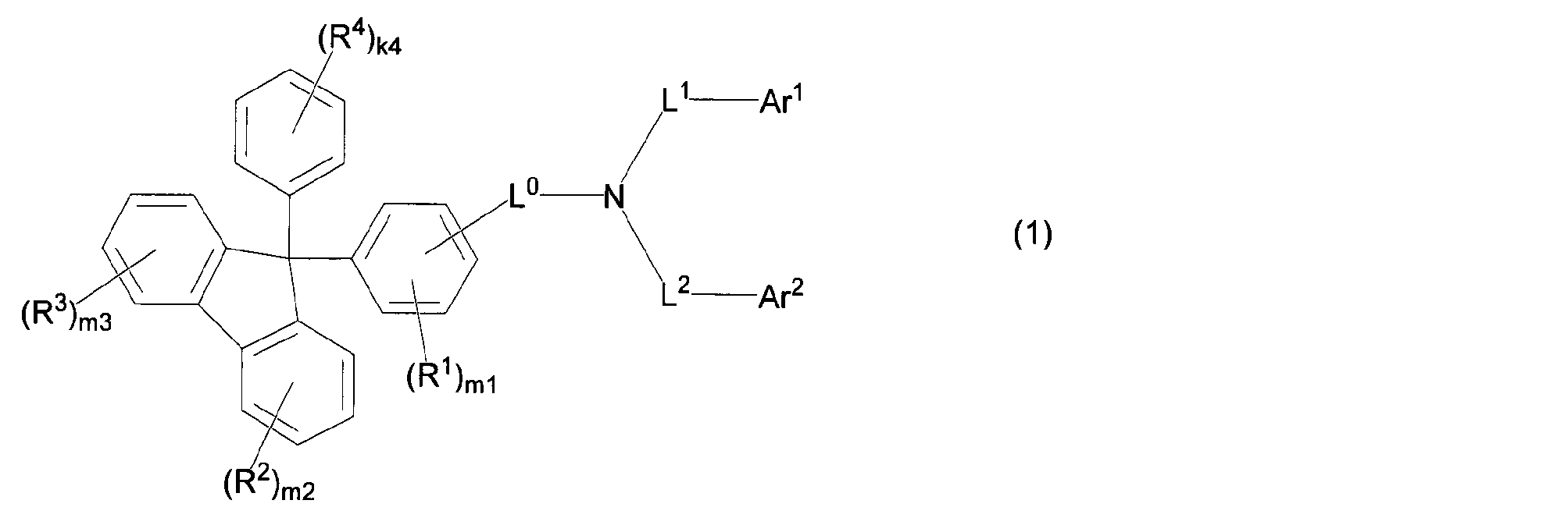
m1~m3は、それぞれ独立に、0~4の整数であり、k4は、0~5の整数である。
L0~L2は、それぞれ独立に、単結合、置換もしくは無置換の環形成炭素数6~50のアリーレン基、又は置換もしくは無置換の環形成原子数5~50のヘテロアリーレン基である。
Ar1は、下記一般式(2)

RA及びRBは、それぞれ独立に、置換もしくは無置換の環形成炭素数6~50のアリール基、置換もしくは無置換の環形成原子数5~50のヘテロアリール基を表し、RA及びRBは、同一であってもよく、互いに異っていてもよい。
R5及びR6は、それぞれ独立に、R1の規定と同じであり、m5及びm6は、それぞれ独立に、0~4の整数である。なお、R5及びR6から選ばれる2つが、互いに結合して、環構造を形成してもよい。)
で表される化合物の1価の残基であり、
上記一般式(2)中のXが-C(RA)(RB)-、-O-、及び-S-のいずれかである化合物の場合、上記一般式(2)中の*1~*4のいずれかの炭素原子と結合している水素原子又はR5が脱離し、当該炭素原子と、前記一般式(1)中のL1又は窒素原子とが結合し、
上記一般式(2)中のXが-NH-である化合物の場合、当該-NH-の窒素原子と結合している水素原子が脱離し、当該窒素原子と、前記一般式(1)中のL1又は窒素原子とが結合する。
Ar2は、置換もしくは無置換の環形成炭素数6~50のアリール基、又は置換もしくは無置換の環形成原子数5~40のヘテロアリール基である。〕
[3]陰極、陽極、及び該陰極と該陽極の間に配置された一層以上の有機薄膜層を有し、該一層以上の有機薄膜層が発光層を含む有機エレクトロルミネッセンス素子であって、
前記一層以上の有機薄膜層の少なくとも1層が、上記[1]に記載の化合物を含む層である、有機エレクトロルミネッセンス素子。
[4]上記[3]に記載の有機エレクトロルミネッセンス素子を搭載した、電子機器。
また、本明細書において、「置換もしくは無置換の原子数XX~YYのZZ基」という表現における「原子数XX~YY」は、ZZ基が無置換である場合の原子数を表すものであり、置換されている場合の置換基の原子数は含めない。
本明細書中において、「ヘテロアリール基」及び「ヘテロアリーレン基」は、環形成原子として、少なくとも1つのヘテロ原子を含む基であり、該へテロ原子としては、窒素原子、酸素原子、硫黄原子、ケイ素原子及びセレン原子から選ばれる1種以上であることが好ましい。
これらの置換基は、さらに上述の任意の置換基により置換されていてもよい。また、これらの置換基は、複数の置換基が互いに結合して環を形成していてもよい。
また、「置換もしくは無置換」との記載における「無置換」とは、これらの置換基で置換されておらず、水素原子が結合していることを意味する。
本発明の一態様において、下記一般式(1)で表される化合物(以下、「化合物(1)」ともいう)が提供される。当該化合物(1)は、有機エレクトロルミネッセンス素子用材料として有用である。
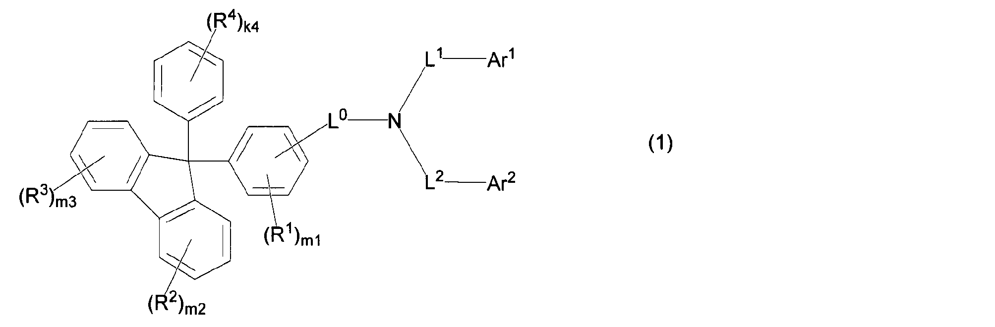
上記一般式(1)において、R1~R4は、一般式(1)中のそれぞれのベンゼン環の置換基を表し、各ベンゼン環の炭素原子と結合する。
R1~R4は、それぞれ独立に、置換もしくは無置換の炭素数1~20(好ましくは1~8、より好ましくは1~3)のアルキル基、置換もしくは無置換の環形成炭素数6~50(好ましくは6~25、より好ましくは6~18、更に好ましくは6~12)のアリール基、置換もしくは無置換の環形成原子数5~50(好ましくは5~10、より好ましくは5~8、更に好ましくは5又は6)のヘテロアリール基、ハロゲン原子、置換もしくは無置換の炭素数1~20(好ましくは1~5、より好ましくは1~4)のフルオロアルキル基、置換もしくは無置換の炭素数1~20(好ましくは1~5、より好ましくは1~4)のアルコキシ基、置換もしくは無置換の炭素数1~20(好ましくは1~5、より好ましくは1~4)のフルオロアルコキシ基、置換もしくは無置換の環形成炭素数6~50(好ましくは6~25、より好ましくは6~18、更に好ましくは6~12)のアリールオキシ基、又はシアノ基を表す。
また、本発明の一態様において、R1~R4から選ばれる2つが互いに結合して環構造を形成することはない。
また、k4は、0~5の整数であり、好ましくは0~2の整数、より好ましくは0又は1、更に好ましくは0である。
なお、m1、m2、m3、k4が0である場合、それぞれのベンゼン環は、無置換であることを意味する。
これらの中でも、メチル基、エチル基、n-プロピル基、イソプロピル基、n-ブチル基、イソブチル基、s-ブチル基、t-ブチル基、及びペンチル基(異性体基を含む)が好ましく、メチル基、エチル基、n-プロピル基、イソプロピル基、n-ブチル基、イソブチル基、s-ブチル基、及びt-ブチル基がより好ましく、メチル基及びt-ブチル基が更に好ましい。
これらの中でも、フェニル基、ナフチルフェニル基、ビフェニルイル基、ターフェニルイル基、ナフチル基、及び9,9-ジメチルフルオレニル基が好ましく、フェニル基、ビフェニルイル基、ナフチル基、及び9,9-ジメチルフルオレニル基がより好ましく、フェニル基が更に好ましい。
該ヘテロアリール基としては、例えば、ピロリル基、フリル基、チエニル基、ピリジル基、ピリダジニル基、ピリミジニル基、ピラジニル基、トリアジニル基、イミダゾリル基、オキサゾリル基、チアゾリル基、ピラゾリル基、イソオキサゾリル基、イソチアゾリル基、オキサジアゾリル基、チアジアゾリル基、トリアゾリル基、インドリル基、イソインドリル基、ベンゾフラニル基、イソベンゾフラニル基、ベンゾチオフェニル基、インドリジニル基、キノリジニル基、キノリル基、イソキノリル基、シンノリル基、フタラジニル基、キナゾリニル基、キノキサリニル基、ベンズイミダゾリル基、ベンズオキサゾリル基、ベンズチアゾリル基、インダゾリル基、ベンズイソキサゾリル基、ベンズイソチアゾリル基、ジベンゾフラニル基、ジベンゾチオフェニル基、フェナントリジニル基、アクリジニル基、フェナントロリニル基、フェナジニル基、フェノチアジニル基、フェノキサジニル基、及びキサンテニル基等が挙げられる。
これらの中でも、フリル基、チエニル基、ピリジル基、ピリダジニル基、ピリミジニル基、ピラジニル基、トリアジニル基、ベンゾフラニル基、ベンゾチオフェニル基、ジベンゾフラニル基、ジベンゾチオフェニル基が好ましく、ベンゾフラニル基、ベンゾチオフェニル基、ジベンゾフラニル基、及びジベンゾチオフェニル基がより好ましい。
具体的なフルオロアルキル基としては、ヘプタフルオロプロピル基、ペンタフルオロエチル基、2,2,2-トリフルオロエチル基、及びトリフルオロメチル基が好ましく、ペンタフルオロエチル基、2,2,2-トリフルオロエチル基、及びトリフルオロメチル基がより好ましく、トリフルオロメチル基が更に好ましい。
具体的な該アルコキシ基としては、t-ブトキシ基、プロポキシ基、エトキシ基、及びメトキシ基が好ましく、エトキシ基、及びメトキシ基がより好ましく、メトキシ基が更に好ましい。
具体的な該フルオロアルコキシ基としては、ヘプタフルオロプロポキシ基、ペンタフルオロエトキシ基、2,2,2-トリフルオロエトキシ基、及びトリフルオロメトキシ基が好ましく、ペンタフルオロエトキシ基、2,2,2-トリフルオロエトキシ基、及びトリフルオロメトキシ基がより好ましく、トリフルオロメトキシ基が更に好ましい。
具体的な該アリールオキシ基としては、フェニルオキシ基、1-ナフチルオキシ基、2-ナフチルオキシ基、4-ビフェニルイルオキシ基、p-ターフェニル-4-イルオキシ基、p-トリルオキシ基が好ましく、フェニルオキシ基、及び2-ナフチルオキシ基がより好ましく、フェニルオキシ基が更に好ましい。
前記一般式(1)において、L0~L2は、それぞれ独立に、単結合、置換もしくは無置換の環形成炭素数6~50(好ましくは6~24、より好ましくは6~12)のアリーレン基、又は置換もしくは無置換の環形成原子数5~50(好ましくは5~10、より好ましくは5~8、更に好ましくは5又は6)のヘテロアリーレン基である。
具体的な該アリーレン基としては、ターフェニルジイル基(異性体基を含む)、ビフェニルジイル基(異性体基を含む)、及びフェニレン基(異性体基を含む)が好ましく、ビフェニルジイル基(異性体基を含む)、及びフェニレン基(異性体基を含む)がより好ましく、o-フェニレン基、m-フェニレン基、及びp-フェニレン基が更に好ましい。
当該へテロアリーレン基としては、前記一般式(1)中のR1~R4として選択し得る、上述の環形成原子数5~50のヘテロアリール基から1個の水素原子を除くことにより得られる2価の基が挙げられる。
具体的な該へテロアリーレン基としては、フリレン基、チエニレン基、ピリジレン基、ピリダジニレン基、ピリミジニレン基、ピラジニレン基、トリアジニレン基、ベンゾフラニレン基、ベンゾチオフェニレン基、ジベンゾフラニレン基、ジベンゾチオフェニレン基が好ましく、ベンゾフラニレン基、ベンゾチオフェニレン基、ジベンゾフラニレン基、及びジベンゾチオフェニレン基がより好ましい。

L1及びL2は、単結合、又は置換もしくは無置換の環形成炭素数6~50のアリーレン基であることが好ましく、単結合、又は下記一般式(i)及び(ii)のいずれかで表される基であることがより好ましい。
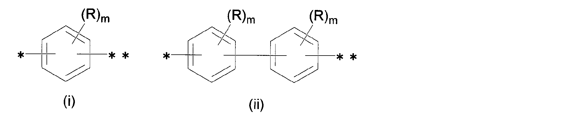
具体的には、*及び**の一方が前記一般式(1)中の窒素原子の結合位置を示し、他方が前記一般式(1)のAr1、Ar2、又は9,9-ジフェニル-9H-フルオレン骨格中のフェニル基の炭素原子との結合位置を示す。
上記式(i)及び(ii)中、Rは、それぞれ独立に、前記一般式(1)中のR1の規定と同じであり、好適な基もR1と同じである。なお、Rは、上記式(i)及び(ii)中のそれぞれのベンゼン環の置換基を表し、各ベンゼン環の炭素原子と結合する。
本発明の一態様において、Rが複数存在する場合、該複数のRは、互いに同一でも異なっていてもよい。また、本発明の一態様において、Rが複数存在する場合に、複数のRから選ばれる2つが、互いに結合して、環構造を形成してもよい。

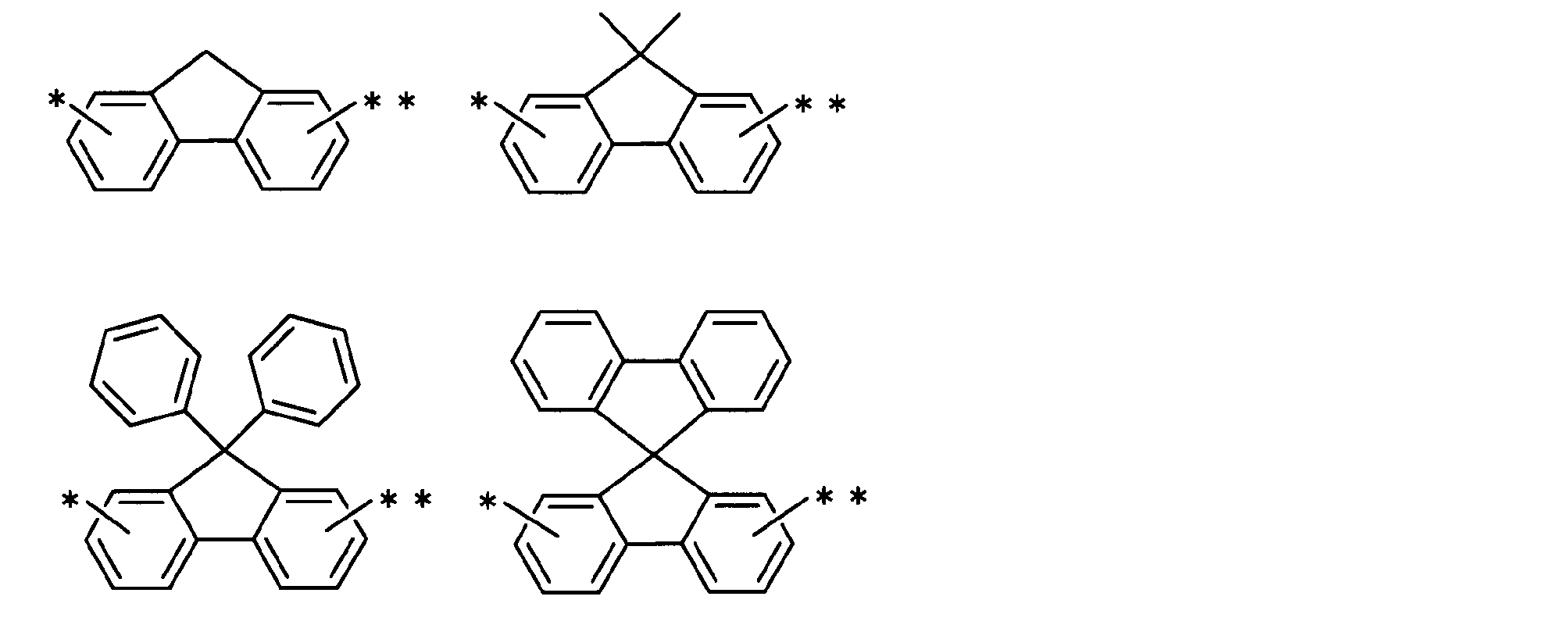
なお、mが0である場合、それぞれのベンゼン環は、無置換であることを意味する。
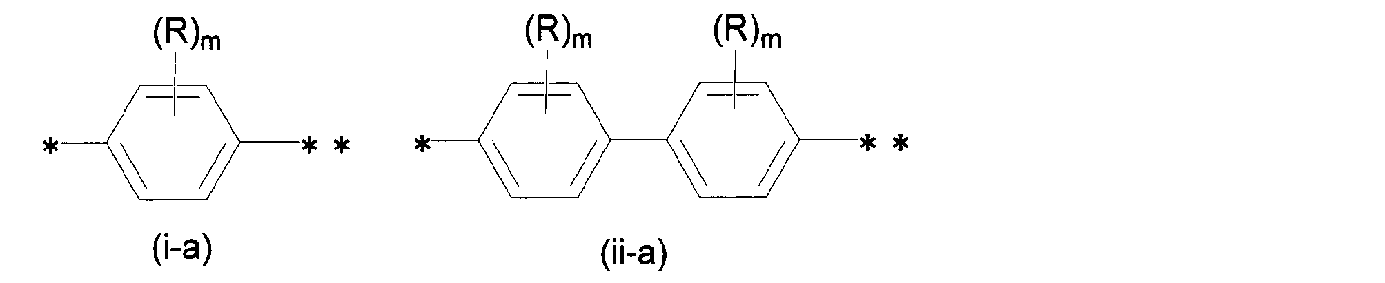
前記一般式(1)において、Ar1は、下記一般式(2)で表される化合物の1価の残基である。
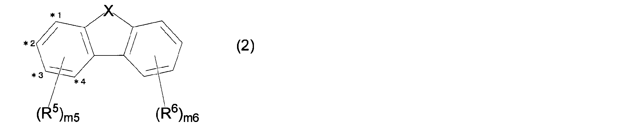
R5及びR6は、それぞれ独立に、前記一般式(1)中のR1の規定と同じであり、好適な基も同じである。なお、R5及びR6は、一般式(2)中のそれぞれのベンゼン環の置換基を表し、各ベンゼン環の炭素原子と結合する。
m5及びm6は、それぞれ独立に、0~4の整数であり、好ましくは0~2、より好ましくは0又は1、更に好ましくは0である。なお、m5、m6が0である場合、それぞれのベンゼン環は、無置換であることを意味する。
なお、本発明の一態様において、R5及びR6が複数存在する場合、該複数のR5及びR6は、互いに同一でも異なっていてもよい。また、本発明の一態様において、R5及びR6から選ばれる2つが、互いに結合して、環構造を形成してもよい。
「環形成炭素数6~50のアリール基」及び「環形成原子数5~50のヘテロアリール基」の具体的な基としては、前記一般式(1)中のR1~R4として選択し得るものと同じアリール基及びヘテロアリール基が挙げられる。
なお、RA及びRBが互いに結合して、環構造を形成することはない。
(I)上記一般式(2)中のXが-C(RA)(RB)-、-O-、及び-S-のいずれかである化合物の場合、上記一般式(2)中の*1~*4のいずれかの炭素原子と結合している水素原子又はR5が脱離し、当該炭素原子と、前記一般式(1)中のL1又は窒素原子とが結合する。
(II)上記一般式(2)中のXが-NH-である化合物の場合、当該-NH-の窒素原子と結合している水素原子が脱離し、当該窒素原子と、前記一般式(1)中のL1又は窒素原子とが結合する。

n5は、それぞれ独立に、0~3の整数であり、好ましくは0~2の整数、より好ましくは0又は1、更に好ましくは0である。*は、前記一般式(1)中のL1又は窒素原子との結合位置を示す。
これらの中でも、Ar1としては、前記一般式(2-2)、(2-5)、(2-7)、(2-9)、(2-11)、及び(2-13)のいずれかで表される基であることが好ましい。
前記一般式(1)において、Ar2は、置換もしくは無置換の環形成炭素数6~50(好ましくは6~25、より好ましくは6~18、更に好ましくは6~12)のアリール基、置換もしくは無置換の環形成原子数5~50(好ましくは5~10、より好ましくは5~8、更に好ましくは5又は6)のヘテロアリール基を表す。
「環形成炭素数6~50のアリール基」及び「環形成原子数5~50のヘテロアリール基」の具体的な基としては、前記一般式(1)中のR1~R4として選択し得るものと同じアリール基及びヘテロアリール基が挙げられる。
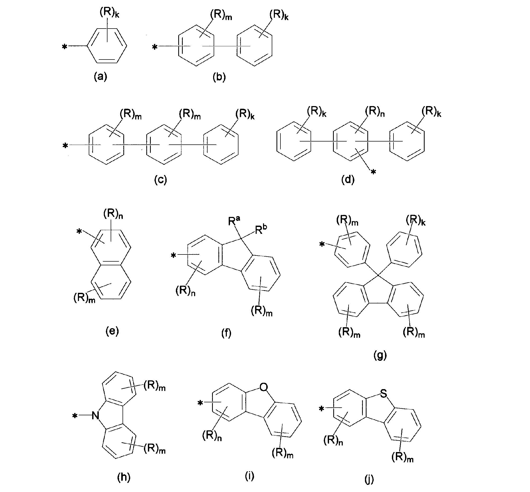
上記一般式(f)中のRa及びRbとしては、水素原子、置換もしくは無置換の炭素数1~20(好ましくは1~8、より好ましくは1~3)のアルキル基、及び置換もしくは無置換の環形成炭素数6~50(好ましくは6~25、より好ましくは6~18、更に好ましくは6~12)のアリール基からなる群より選ばれる基が好ましい。
また、式(f)において、複数のR、Ra、及びRbから選ばれる2つが、互いに結合して、環構造を形成してもよい。
mは、それぞれ独立に、0~4の整数であり、好ましくは0~2の整数、より好ましくは0又は1、更に好ましくは0である。
nは、それぞれ独立に、0~3の整数であり、好ましくは0~2の整数、より好ましくは0又は1、更に好ましくは0である。
なお、k、m、nが0である場合、それぞれのベンゼン環は、無置換であることを意味する。
*は、前記一般式(1)中のL2又は窒素原子との結合位置を示す。
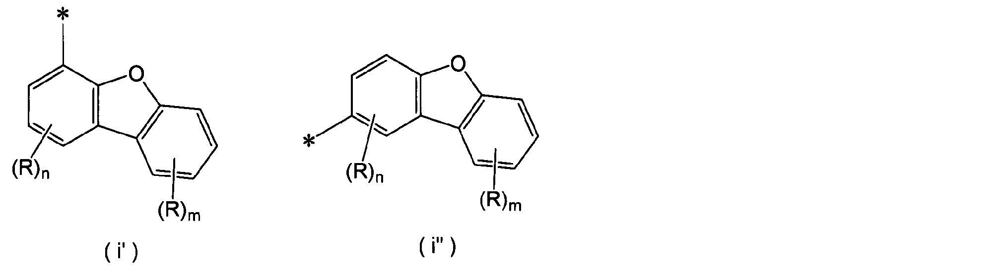

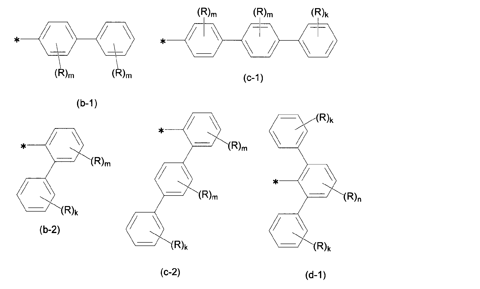


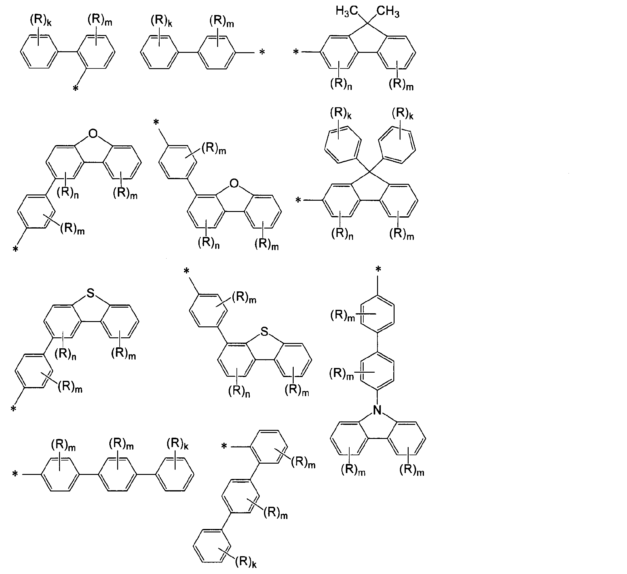
本発明の一態様である化合物(1)としては、下記一般式(1-1)で表される化合物(以下、「化合物(1-1)」ともいう)が好ましい。
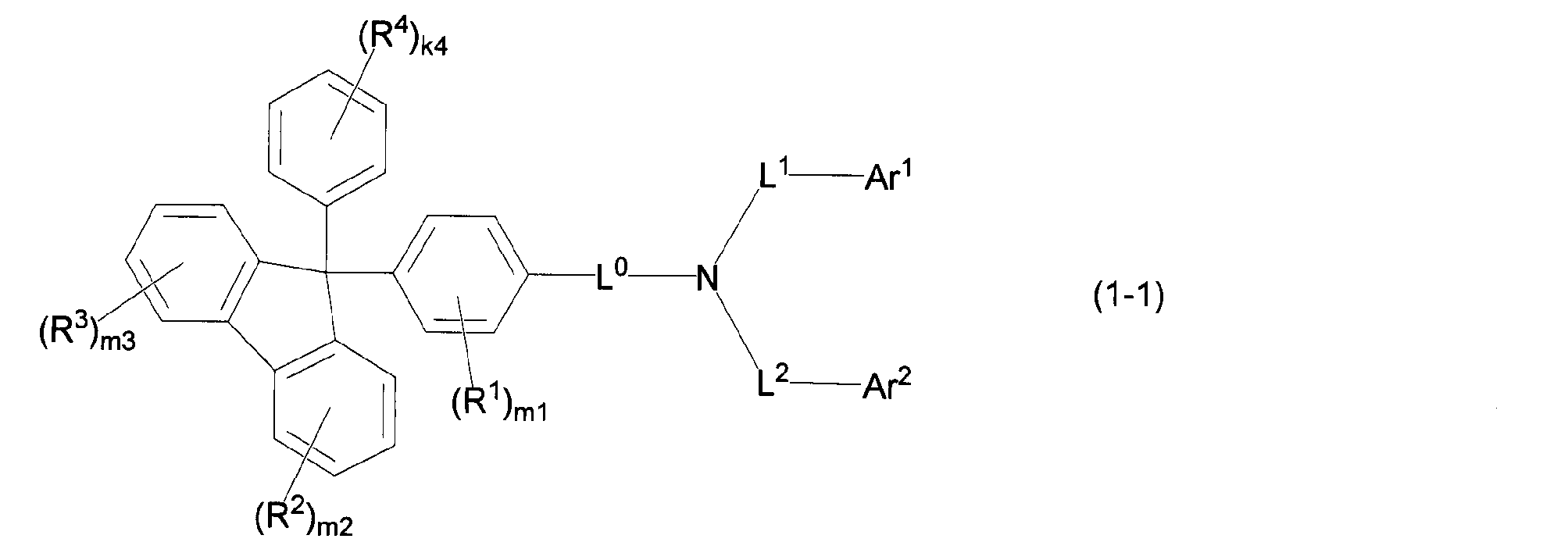
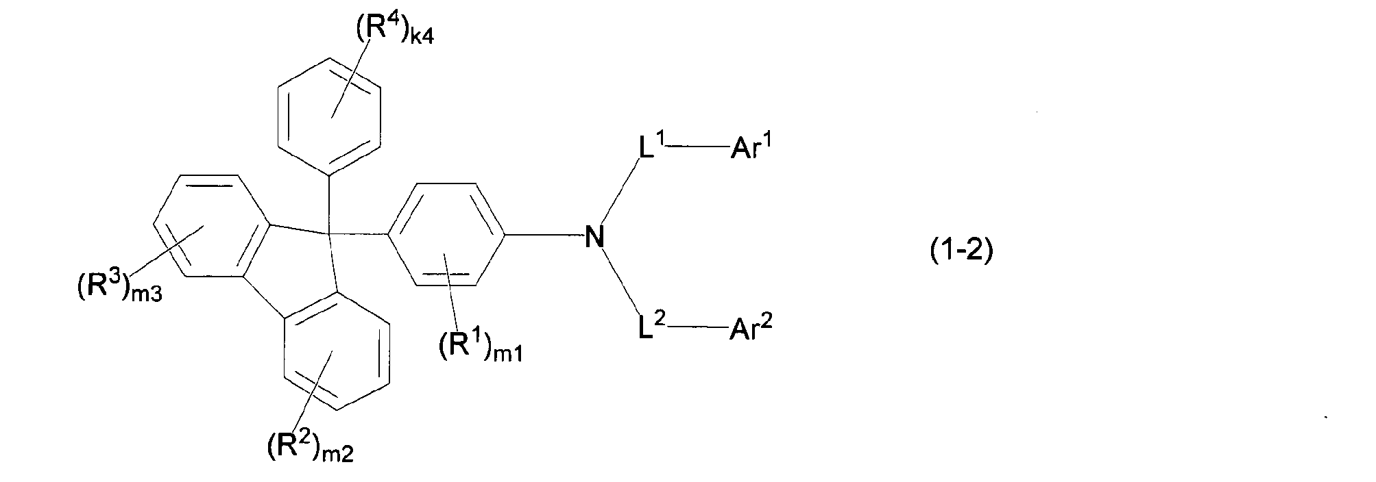
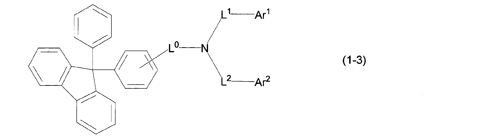

また、R7及びR8は、それぞれ独立に、前記一般式(1)中のR1の規定と同じであり、好適な基についても同じである。
n5は、0~3の整数であり、好ましくは0~2の整数、より好ましくは0又は1、更に好ましくは0である。
k7及びk8は、それぞれ独立に、0~5の整数であり、好ましくは0~2の整数、より好ましくは0又は1、更に好ましくは0である。
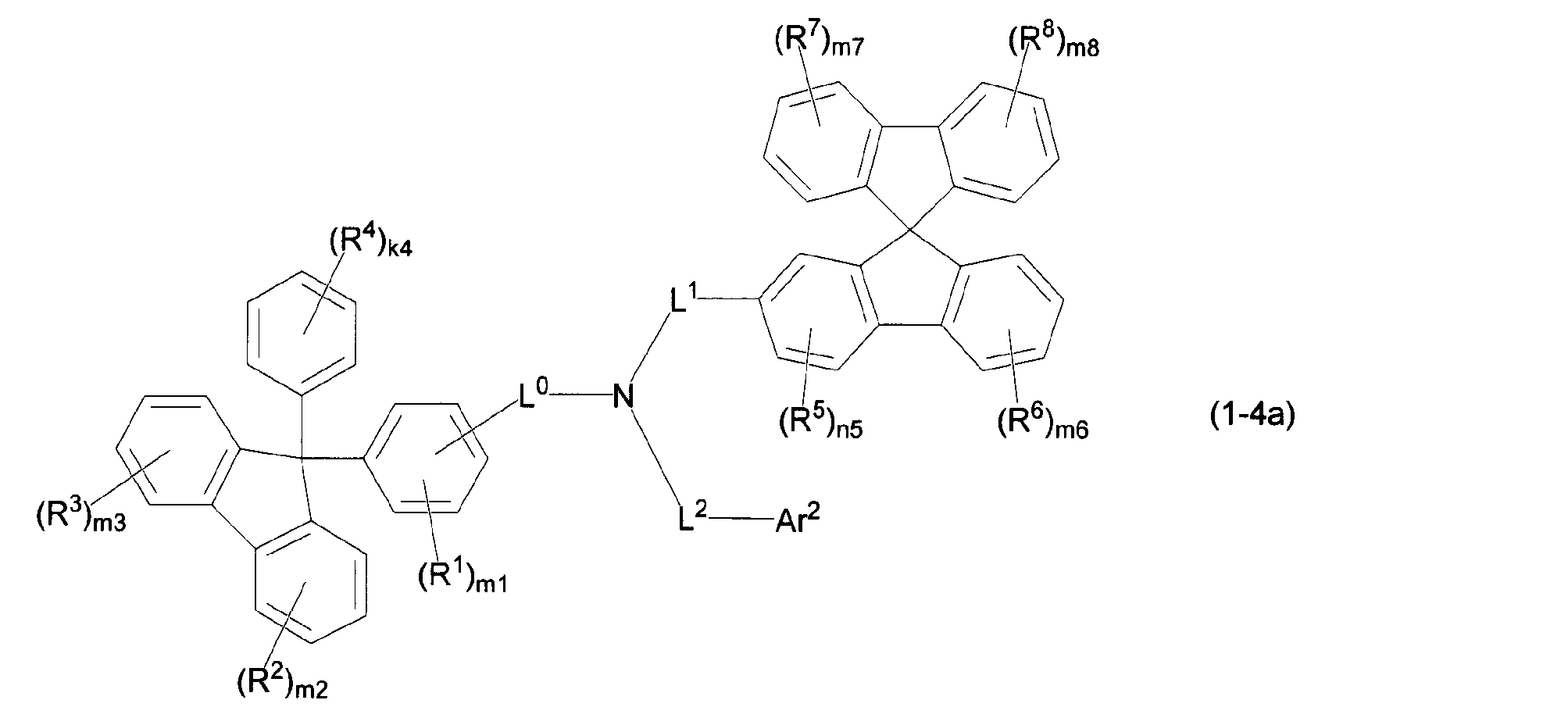
m7及びm8は、それぞれ独立に、0~4の整数であり、好ましくは0~2の整数、より好ましくは0又は1、更に好ましくは0である。
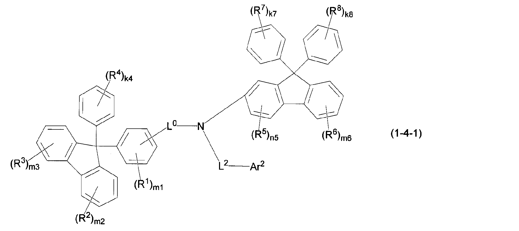

n5は、0~3の整数であり、好ましくは0~2の整数、より好ましくは0又は1、更に好ましくは0である。
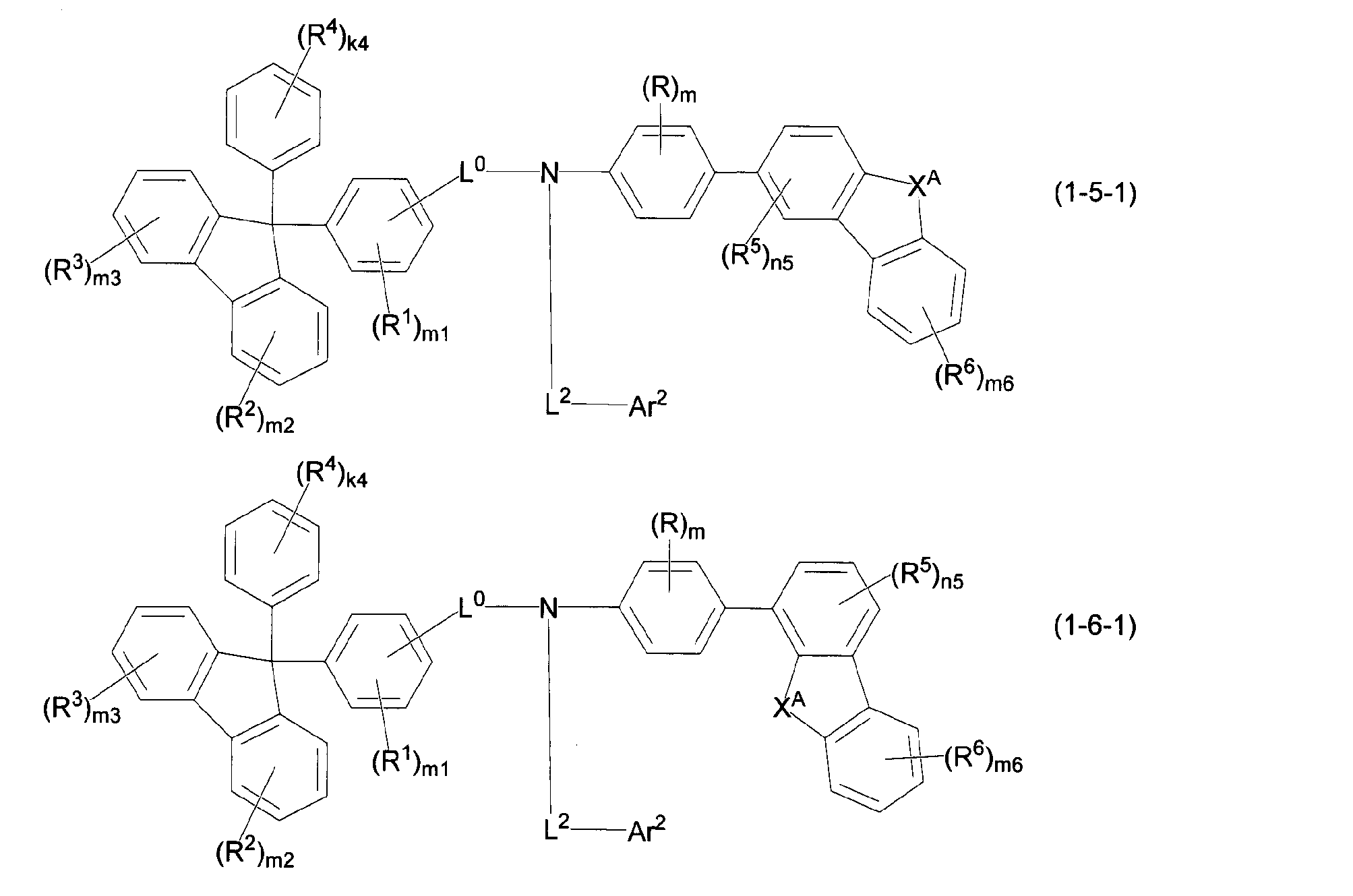
また、Rは、前記一般式(1)中のR1の規定と同じであり、好適な基についても同じである。mは、0~4の整数であり、好ましくは0~2の整数、より好ましくは0又は1、更に好ましくは0である。

なお、本発明の一態様である化合物(1-7)の中でも、下記一般式(1-7-1)で表される化合物(以下、「化合物(1-7-1)」ともいう)又は下記一般式(1-7-2)で表される化合物(以下、「化合物(1-7-2)」ともいう)がより好ましい。
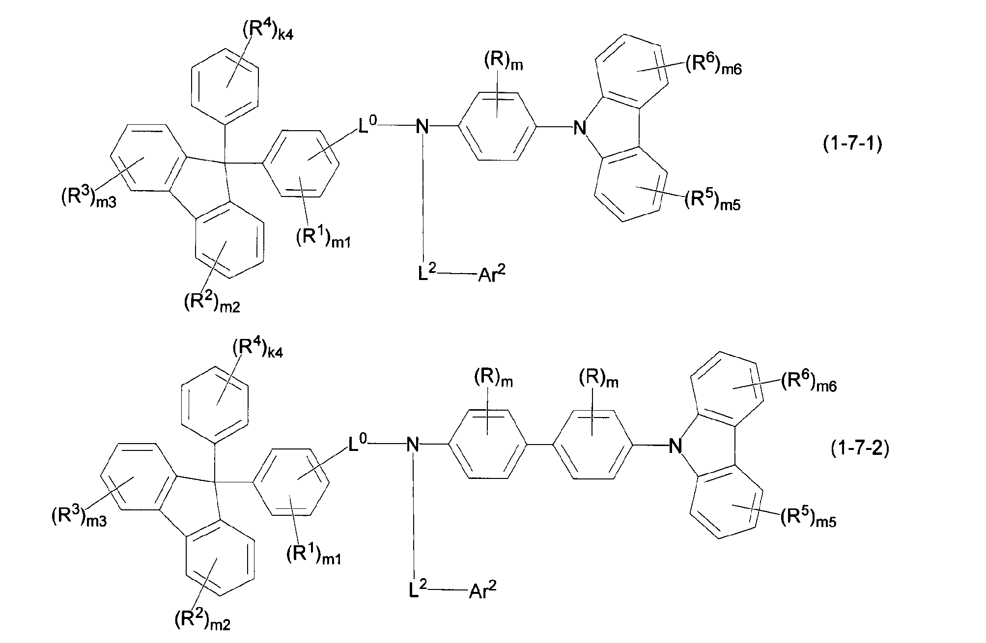
また、Rは、前記一般式(1)中のR1の規定と同じであり、好適な基についても同じである。mは、それぞれ独立に、0~4の整数であり、好ましくは0~2の整数、より好ましくは0又は1、更に好ましくは0である。

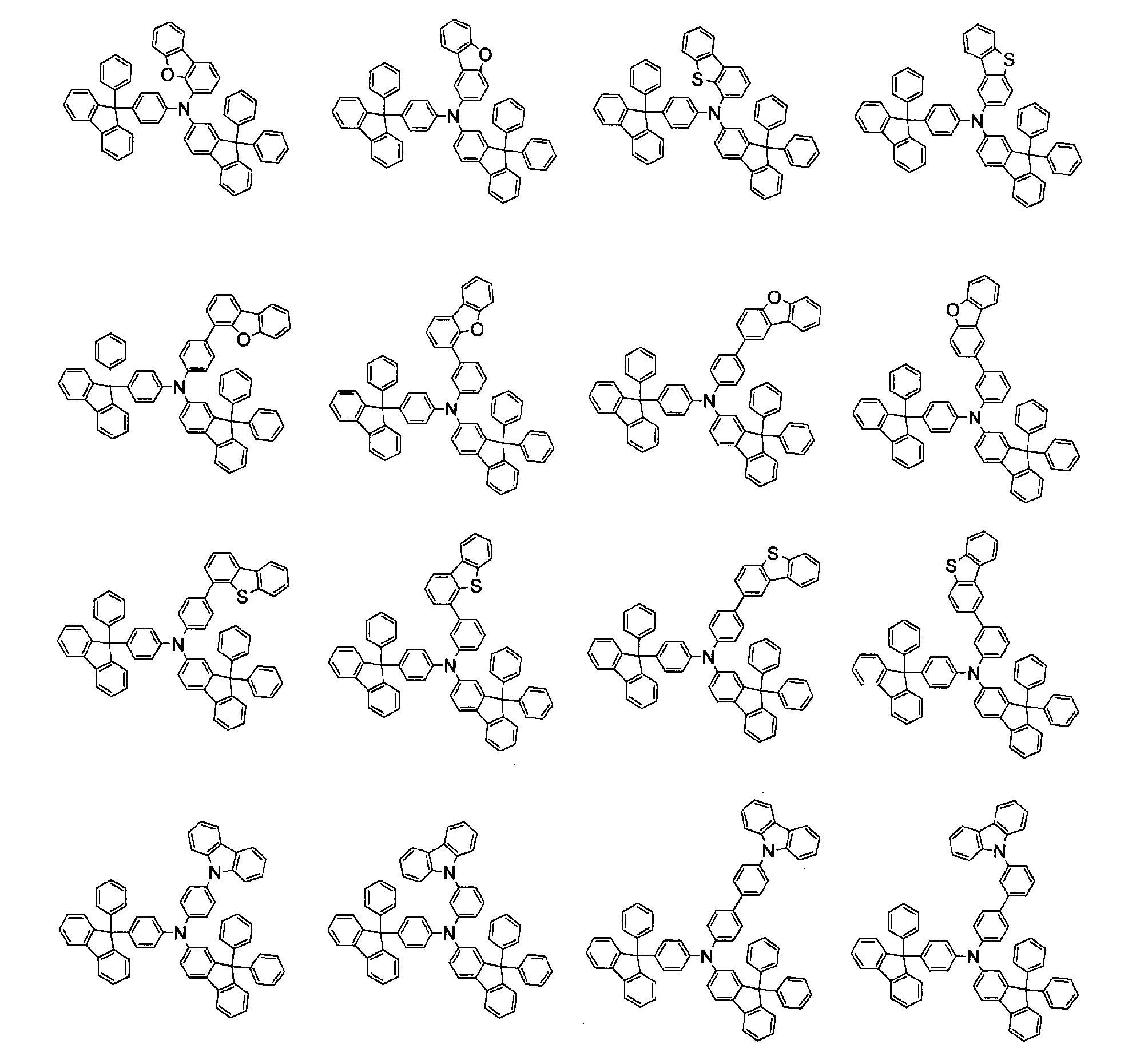
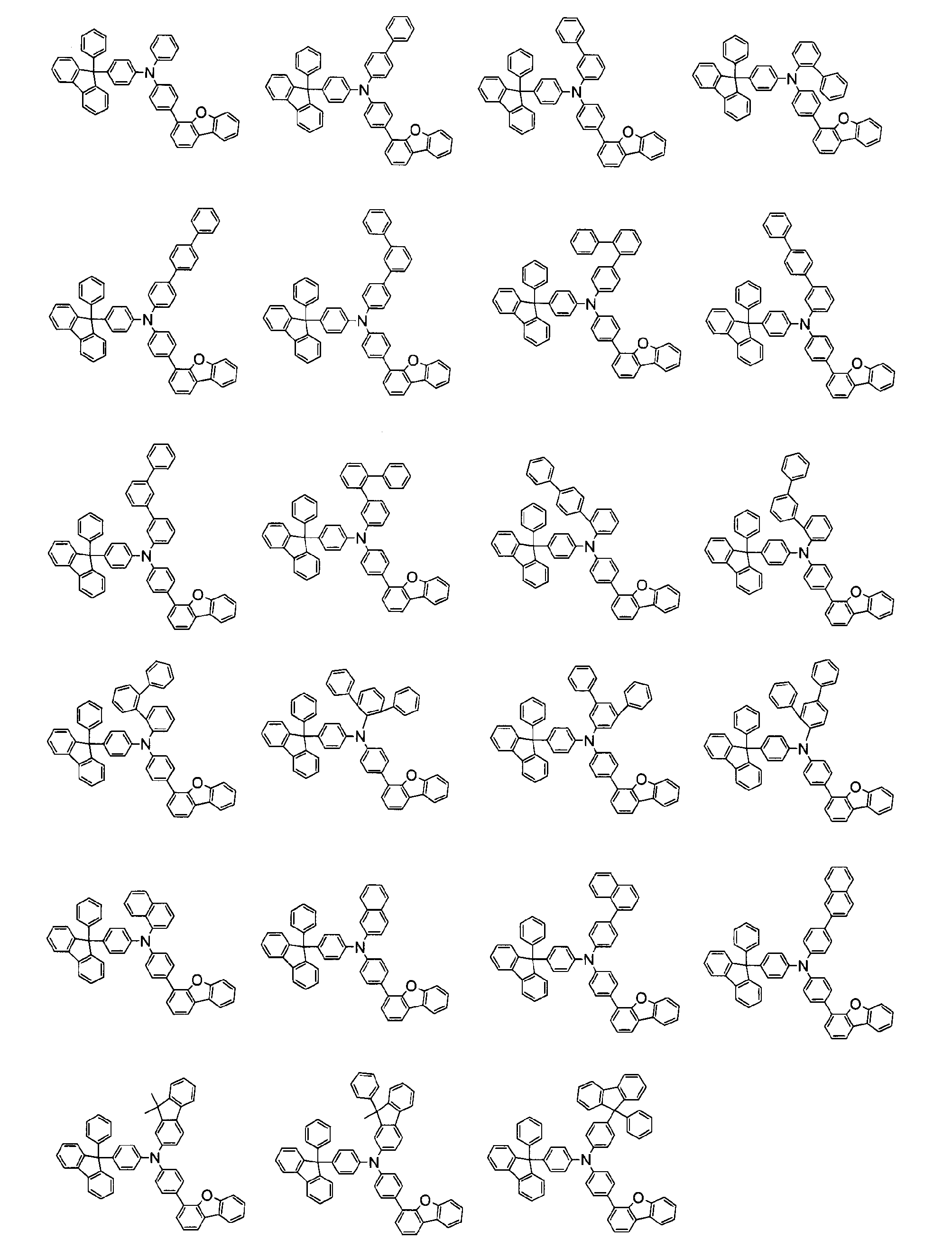
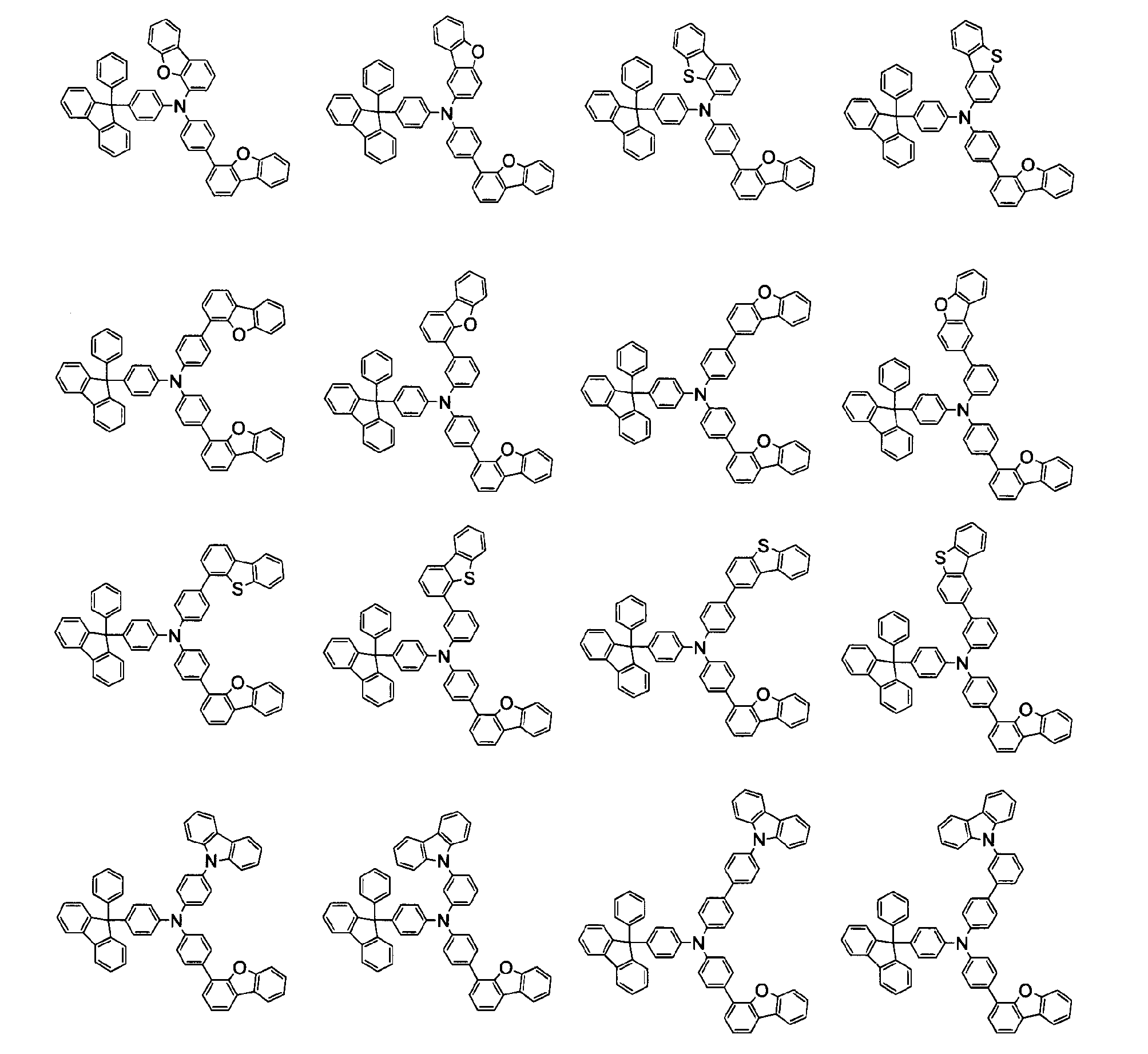


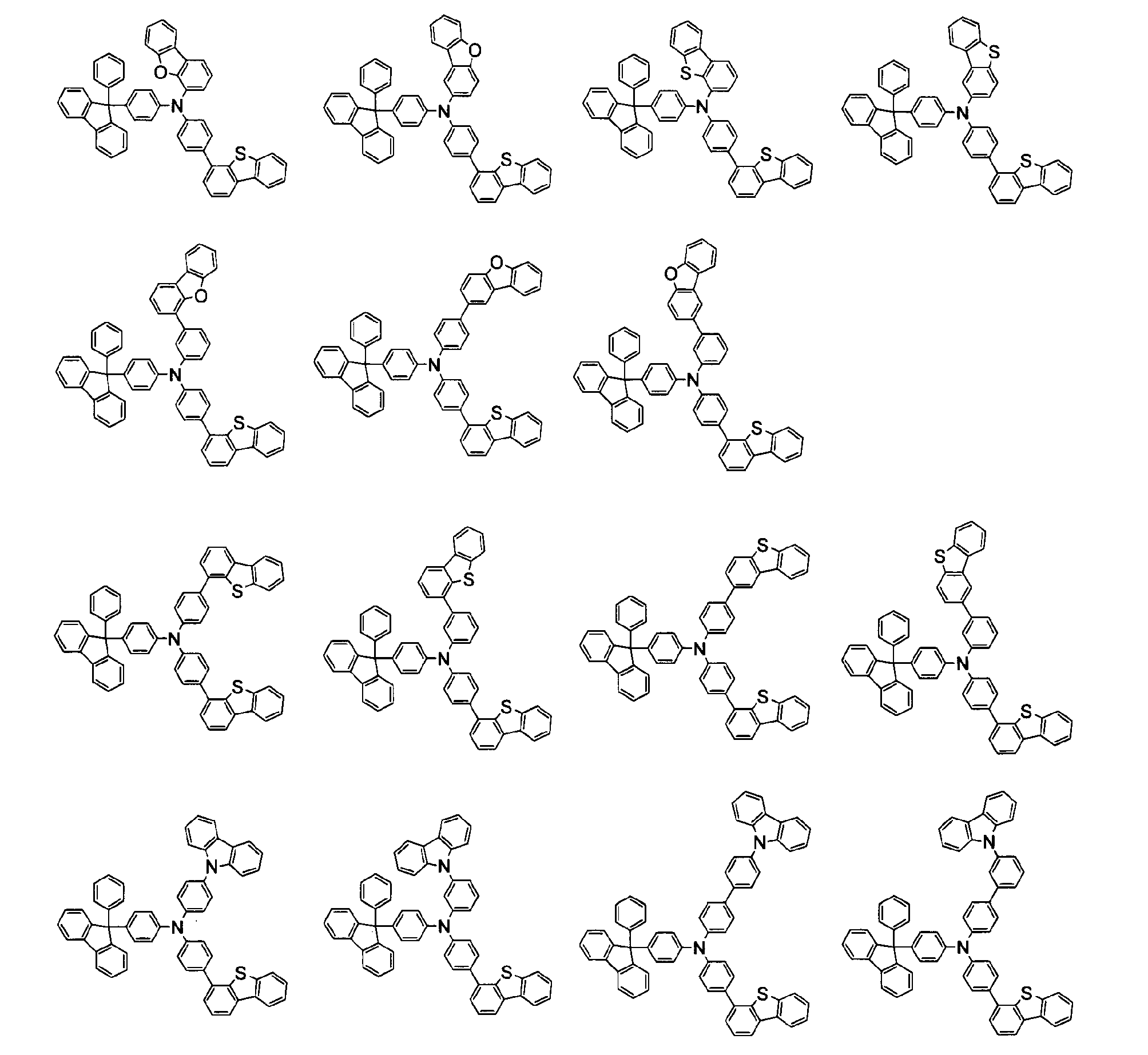

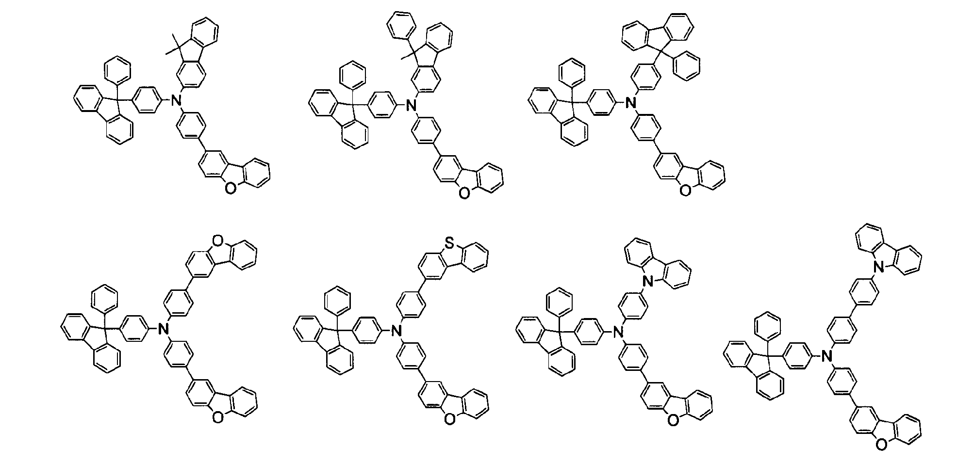
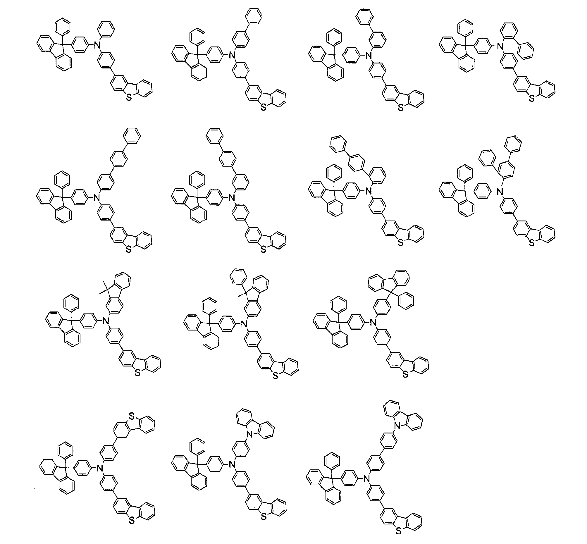
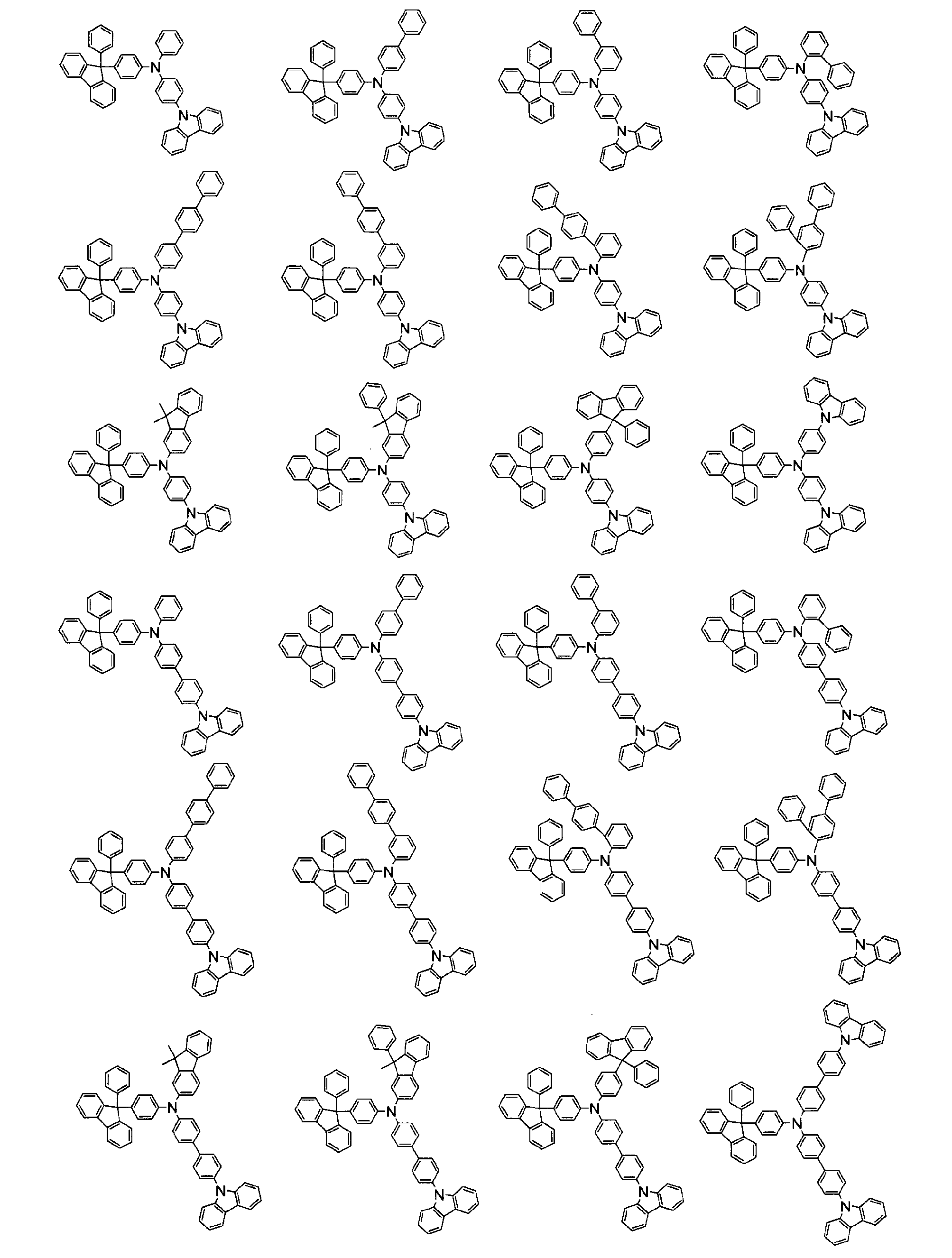


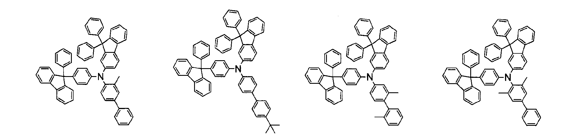

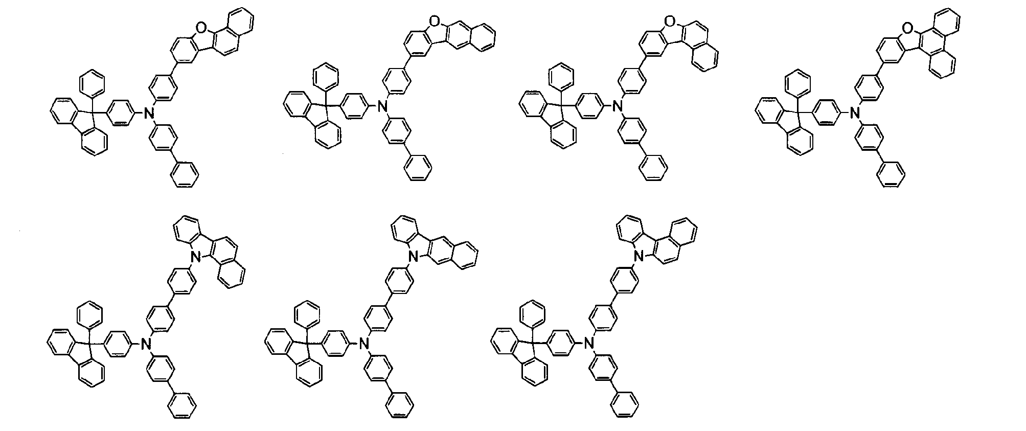
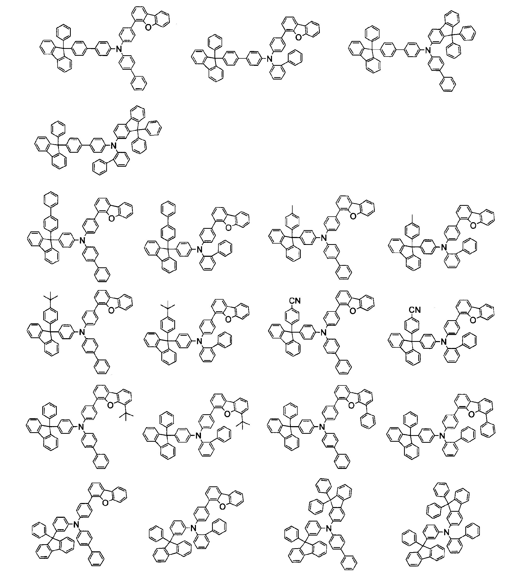

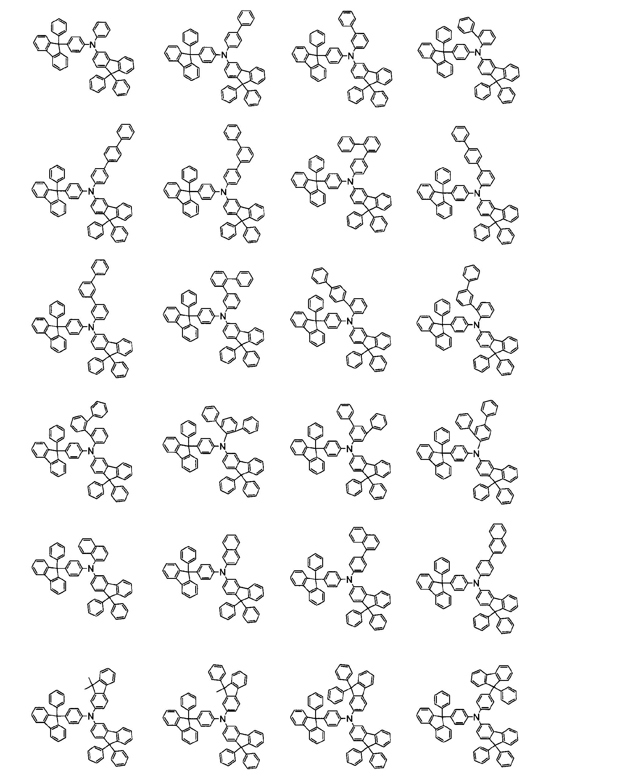
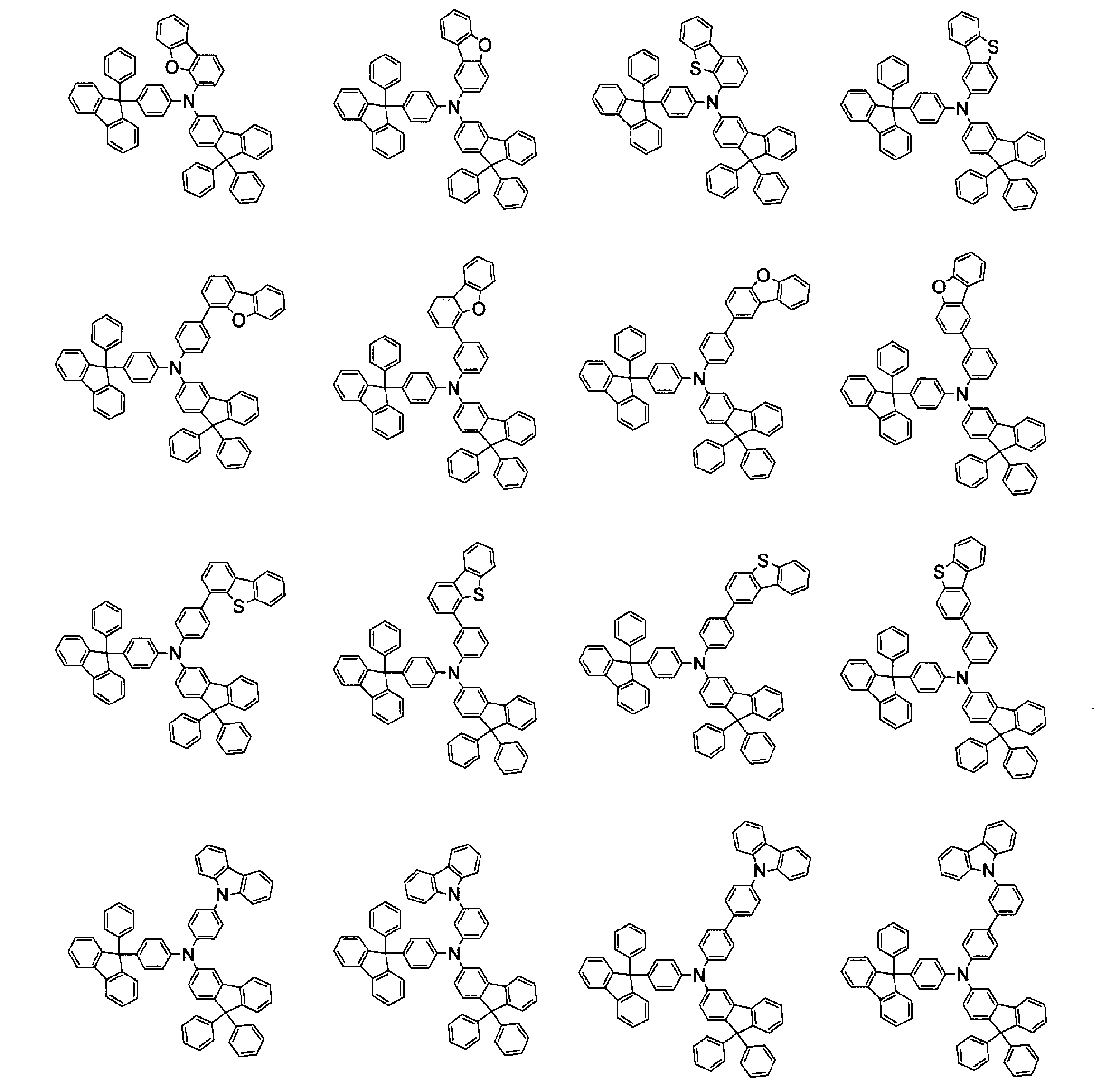

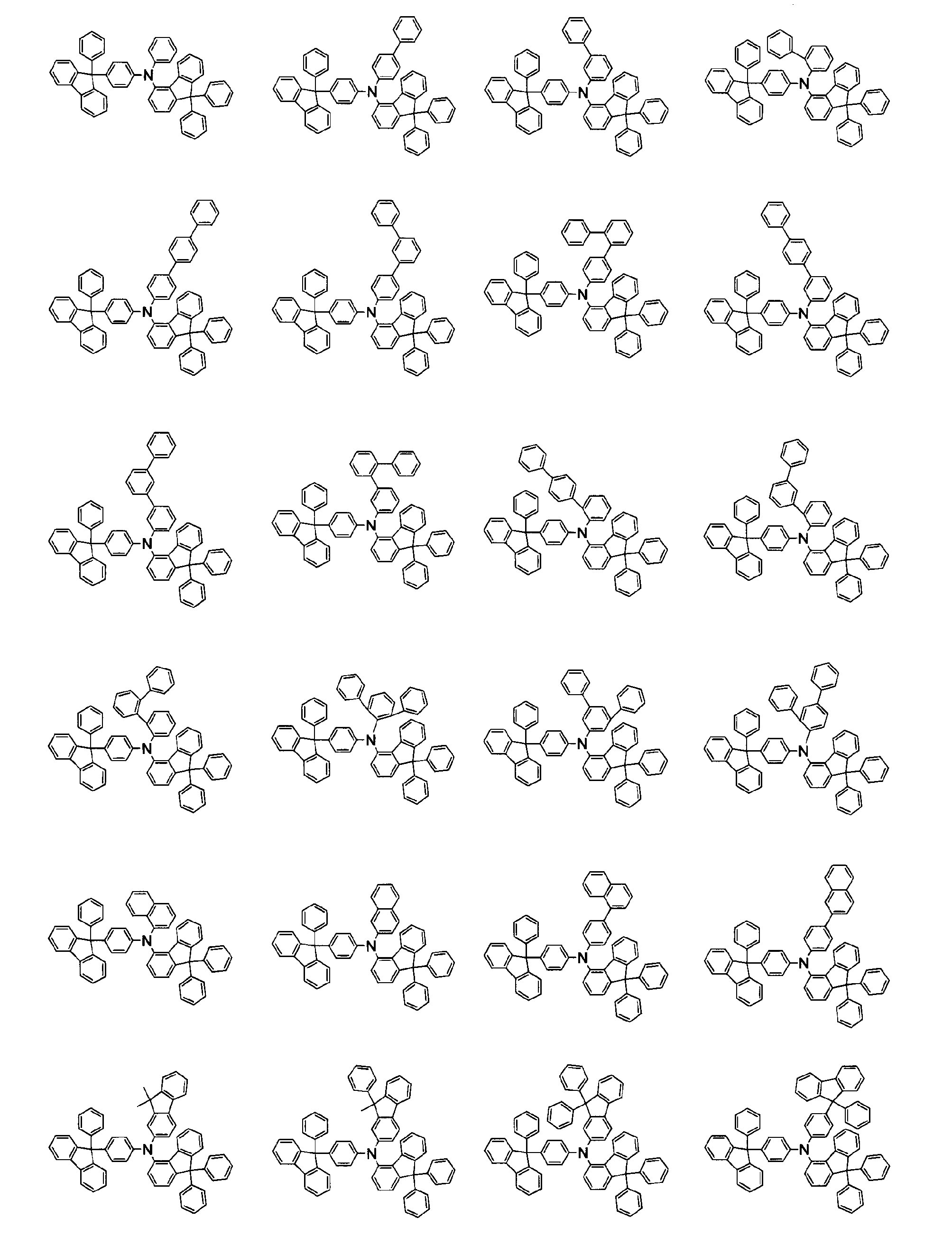
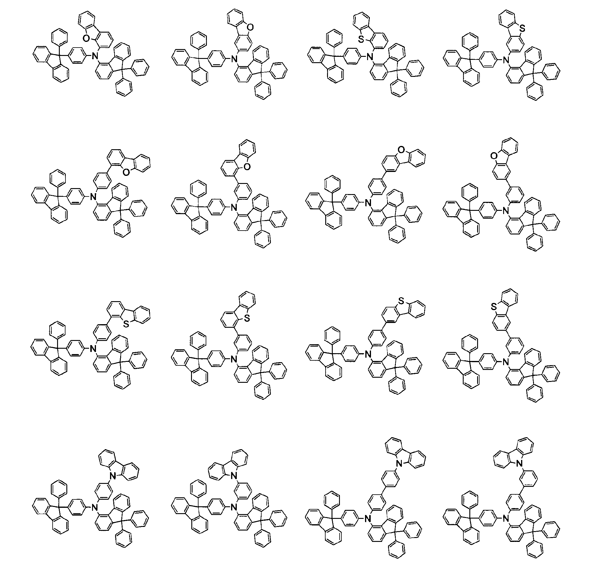

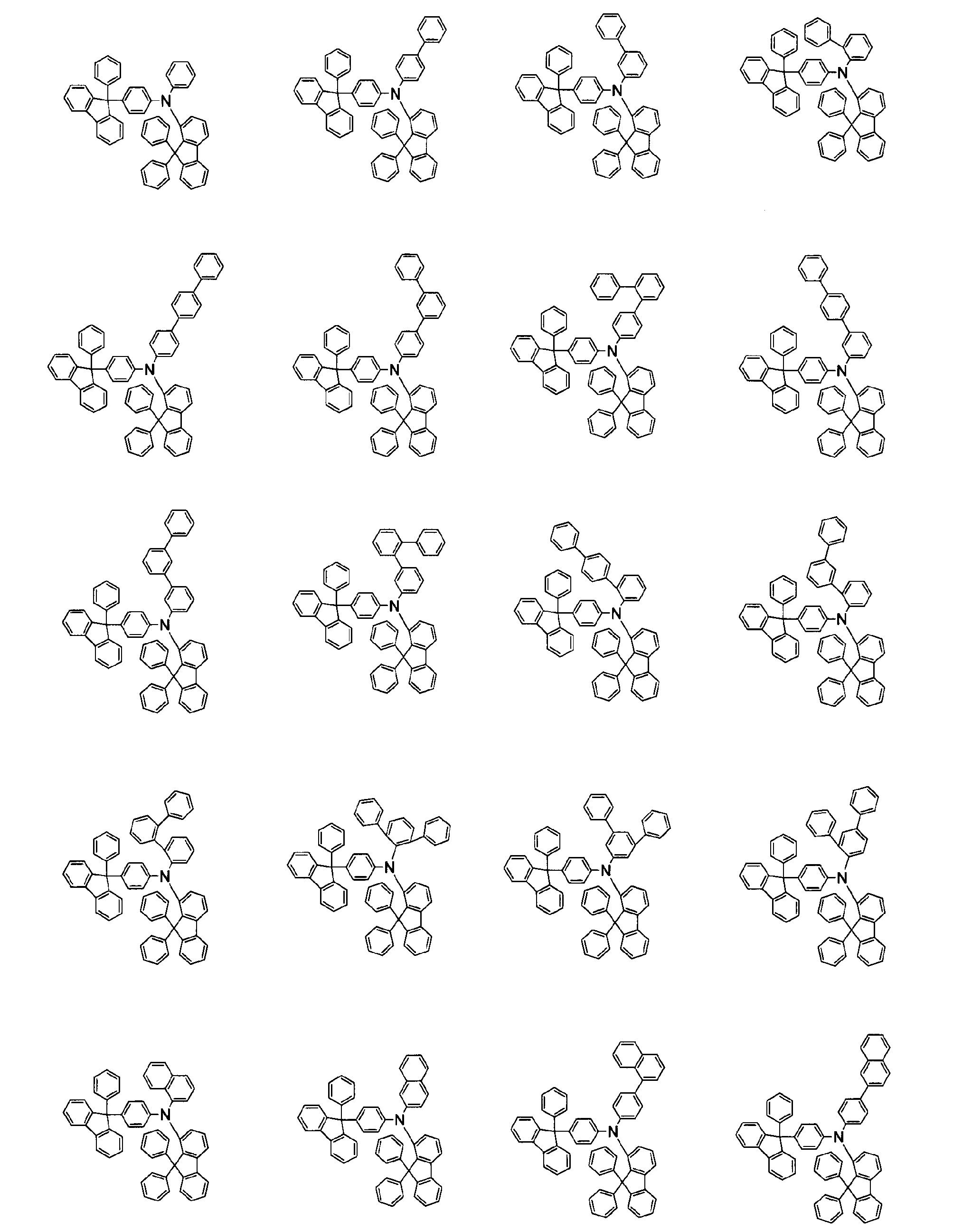


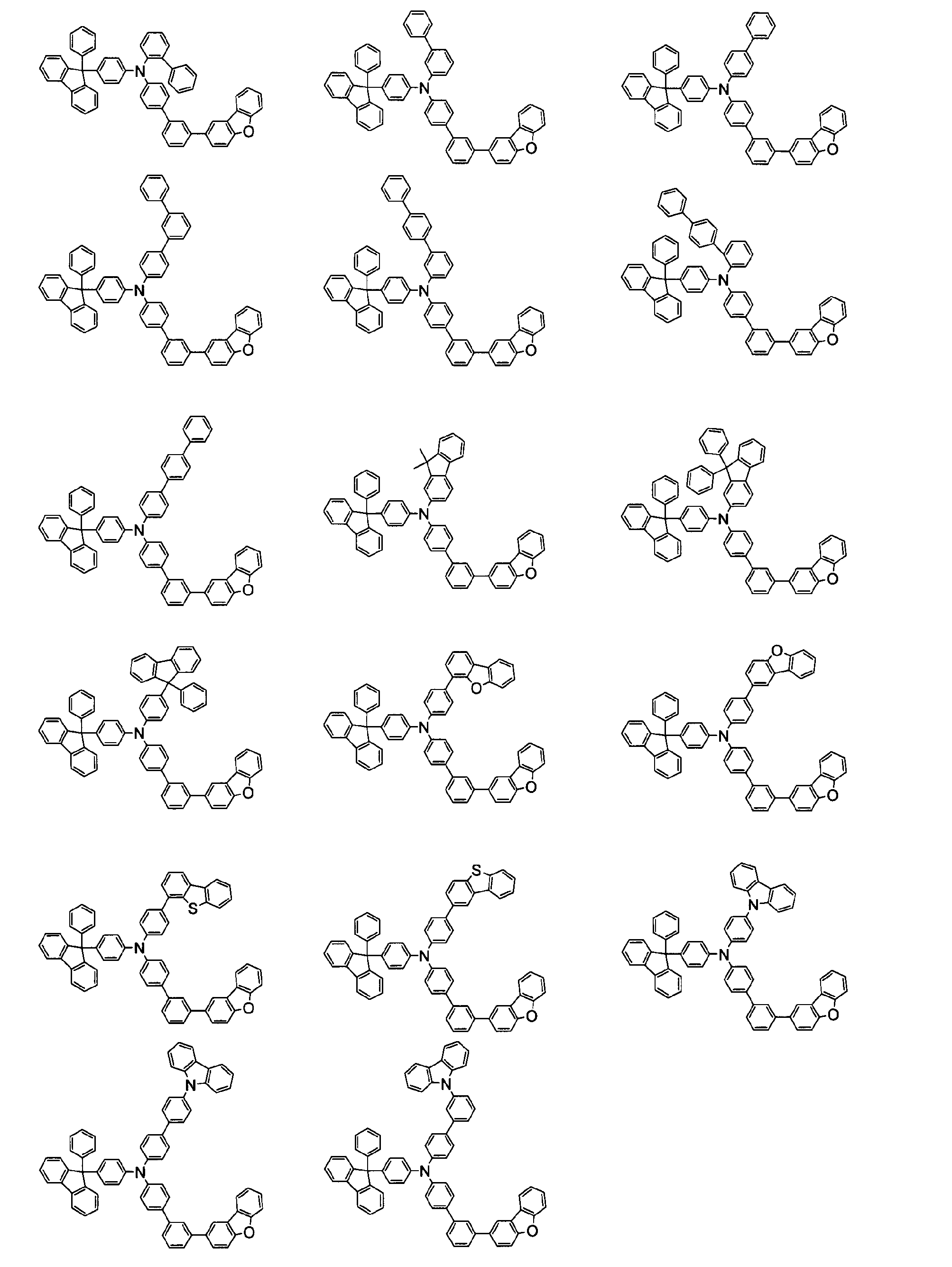
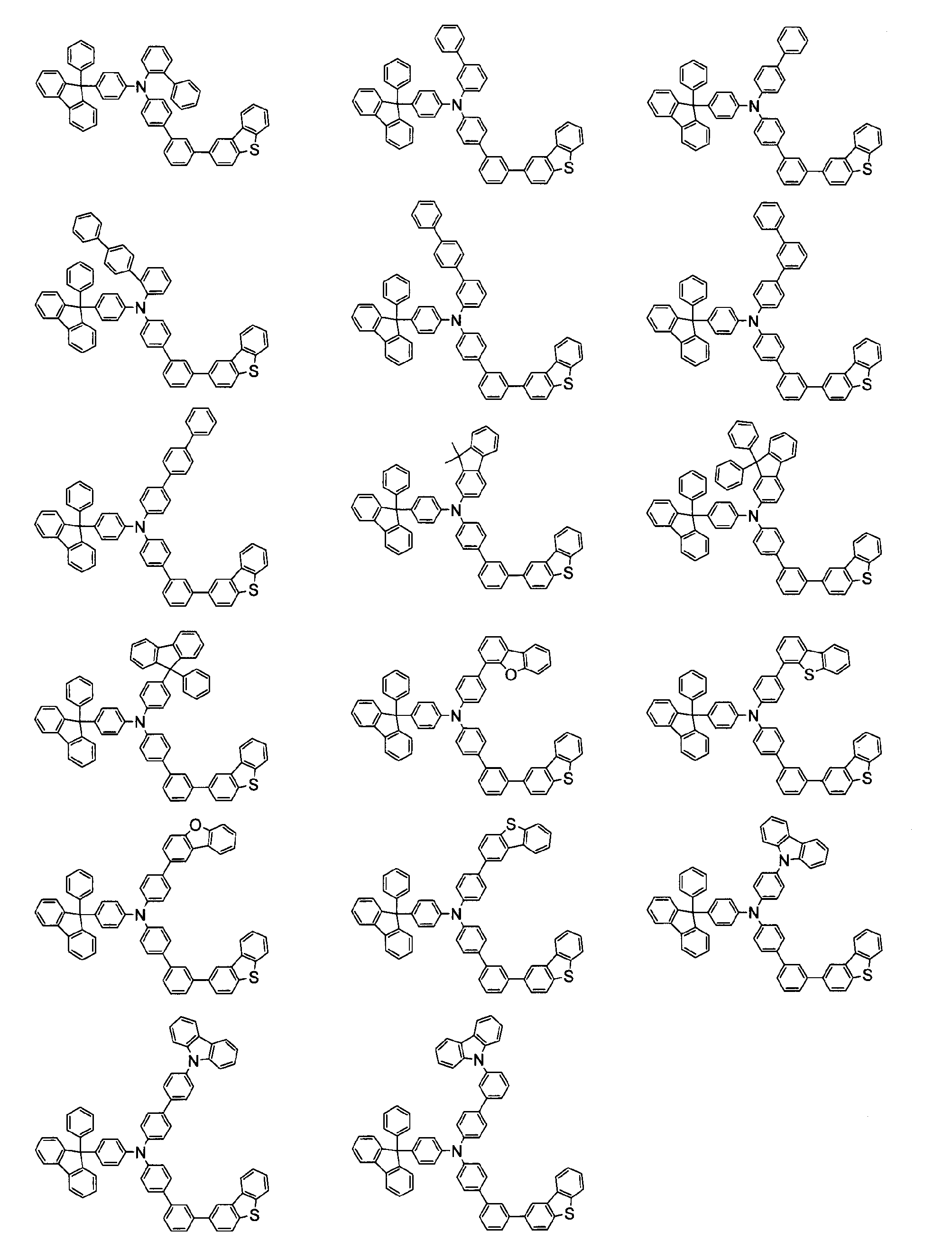
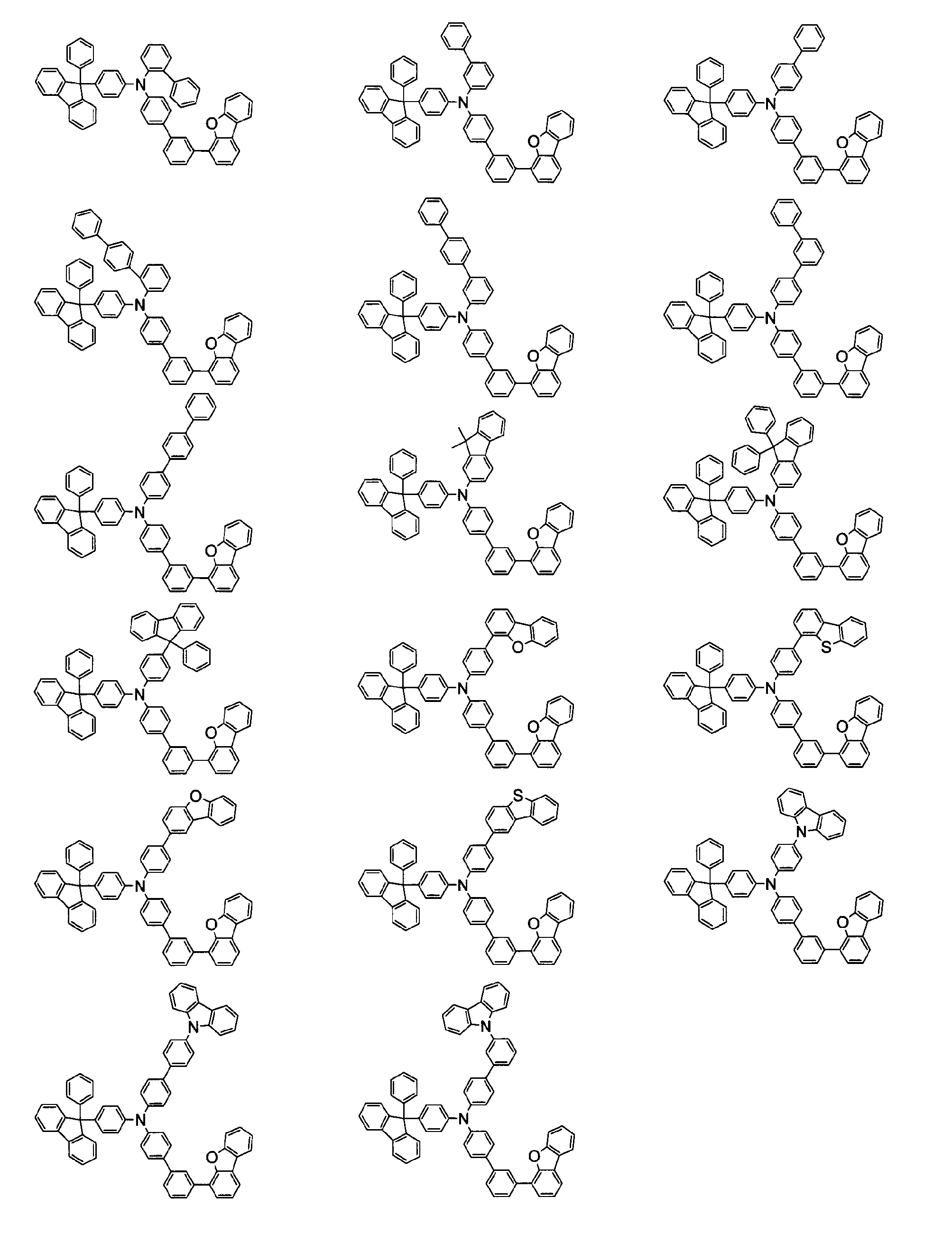
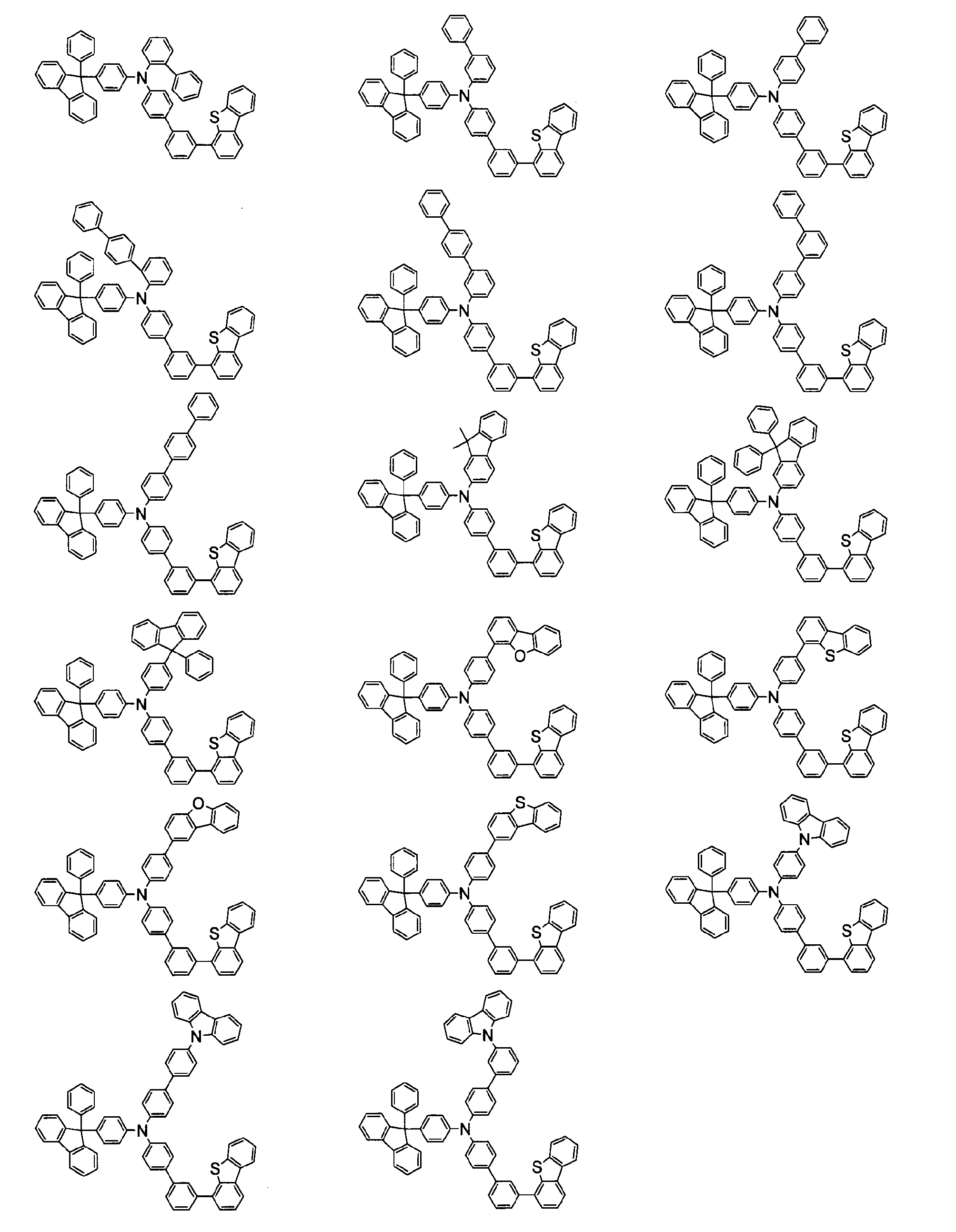

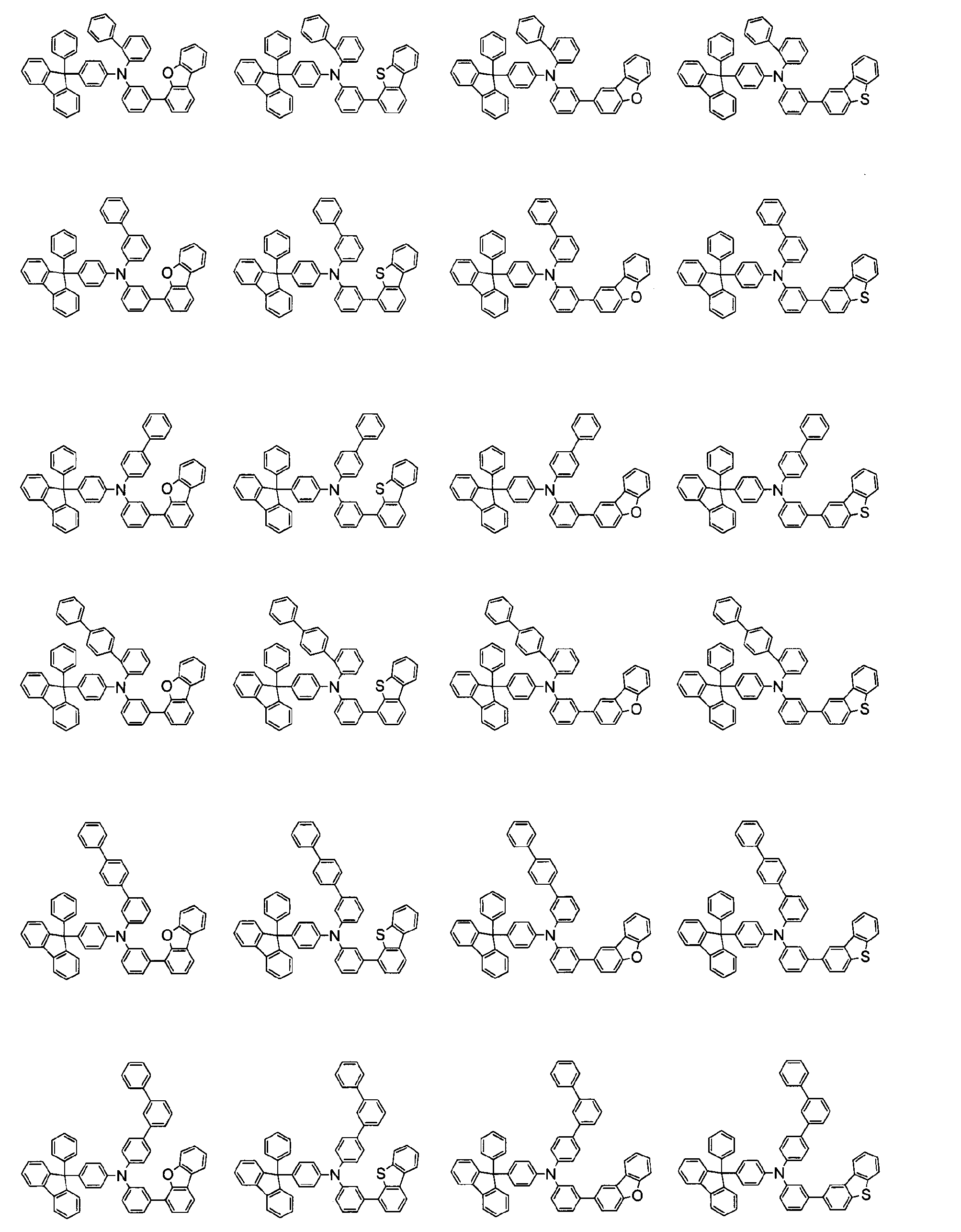

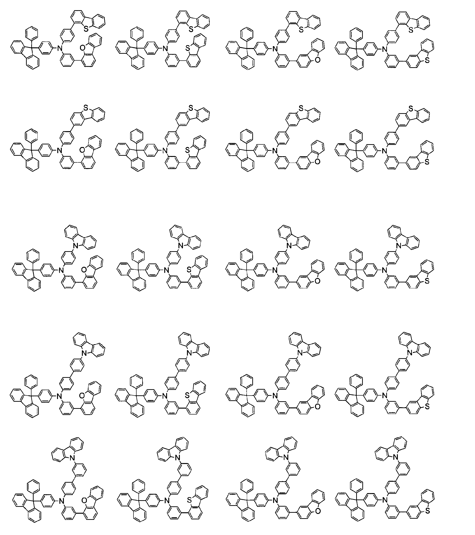
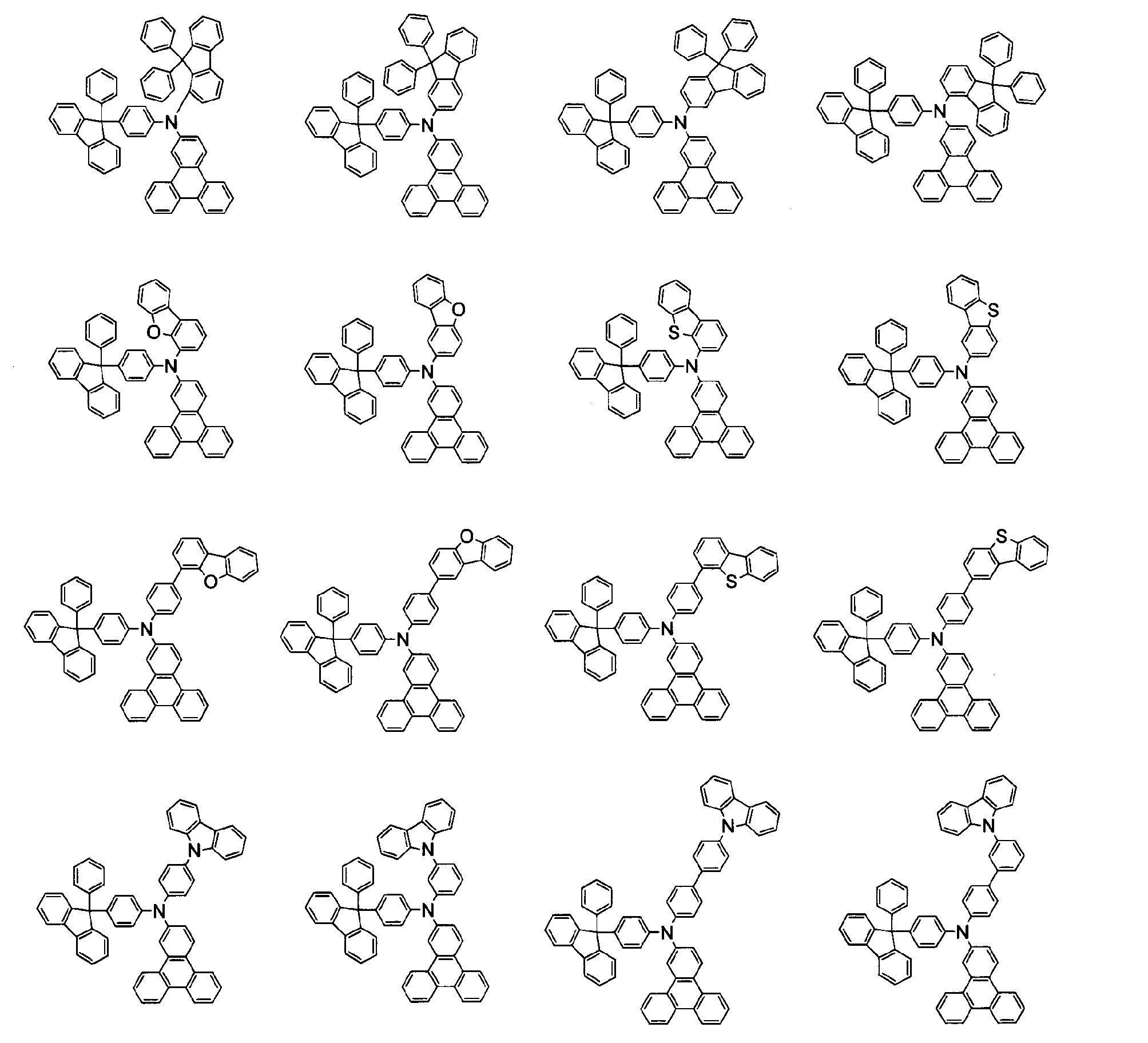
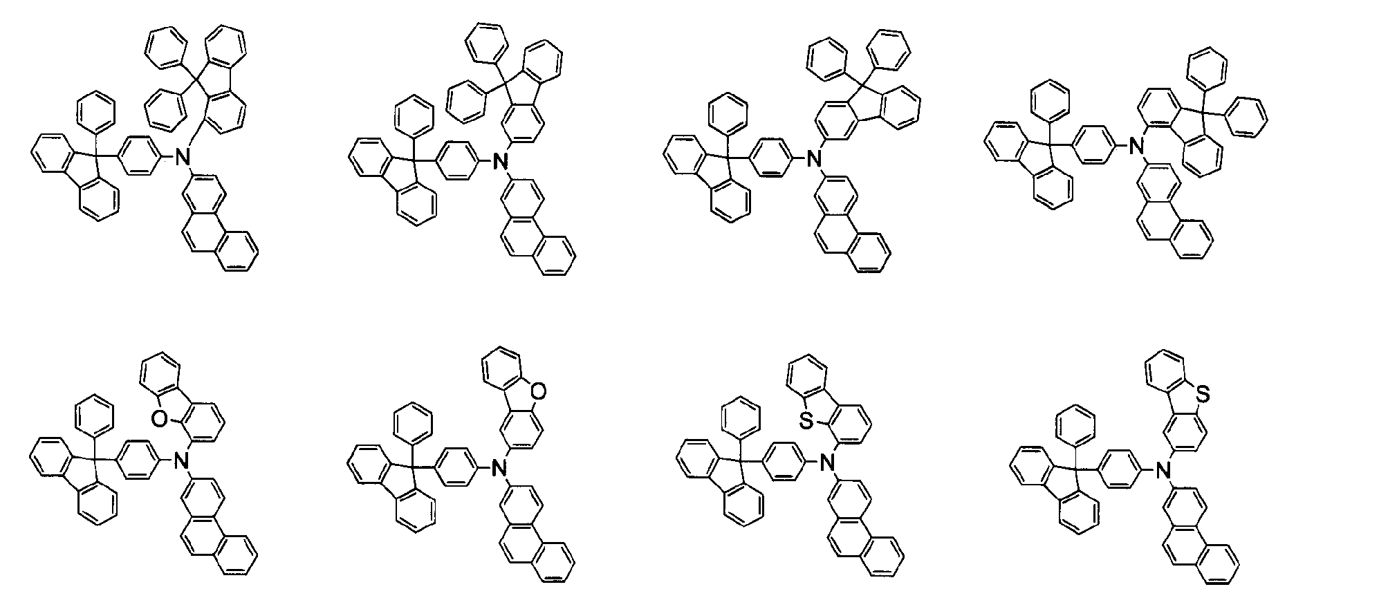
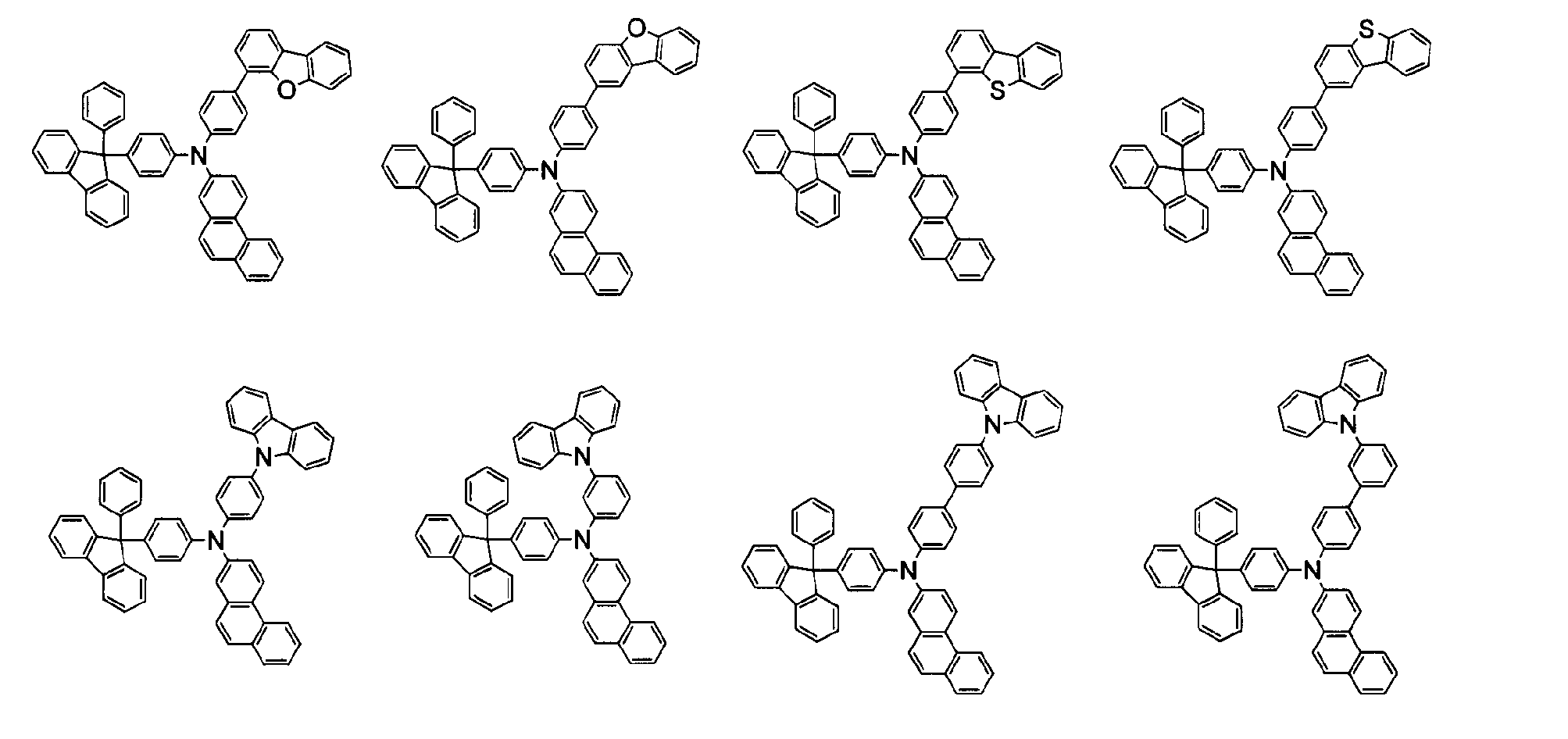
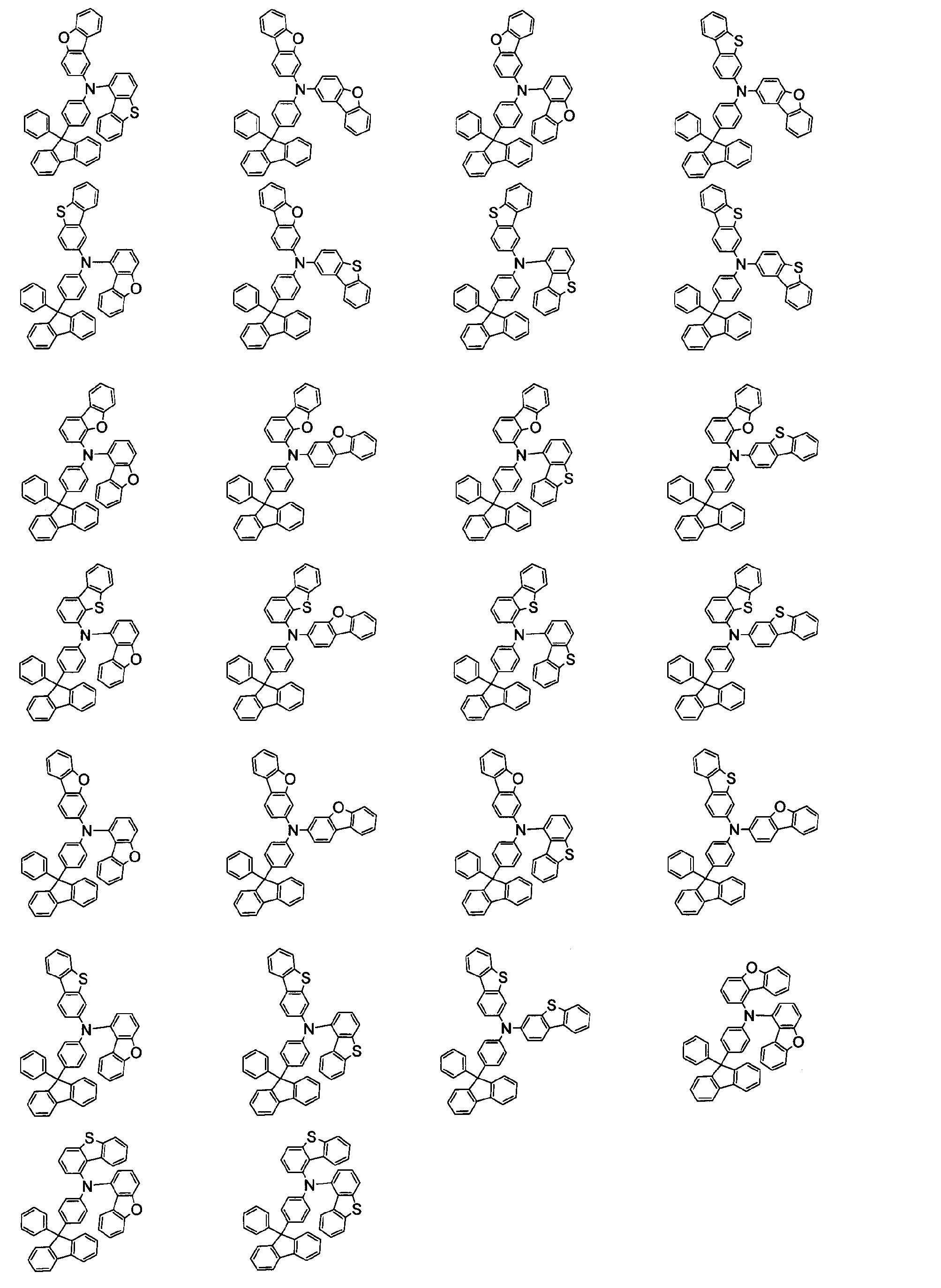

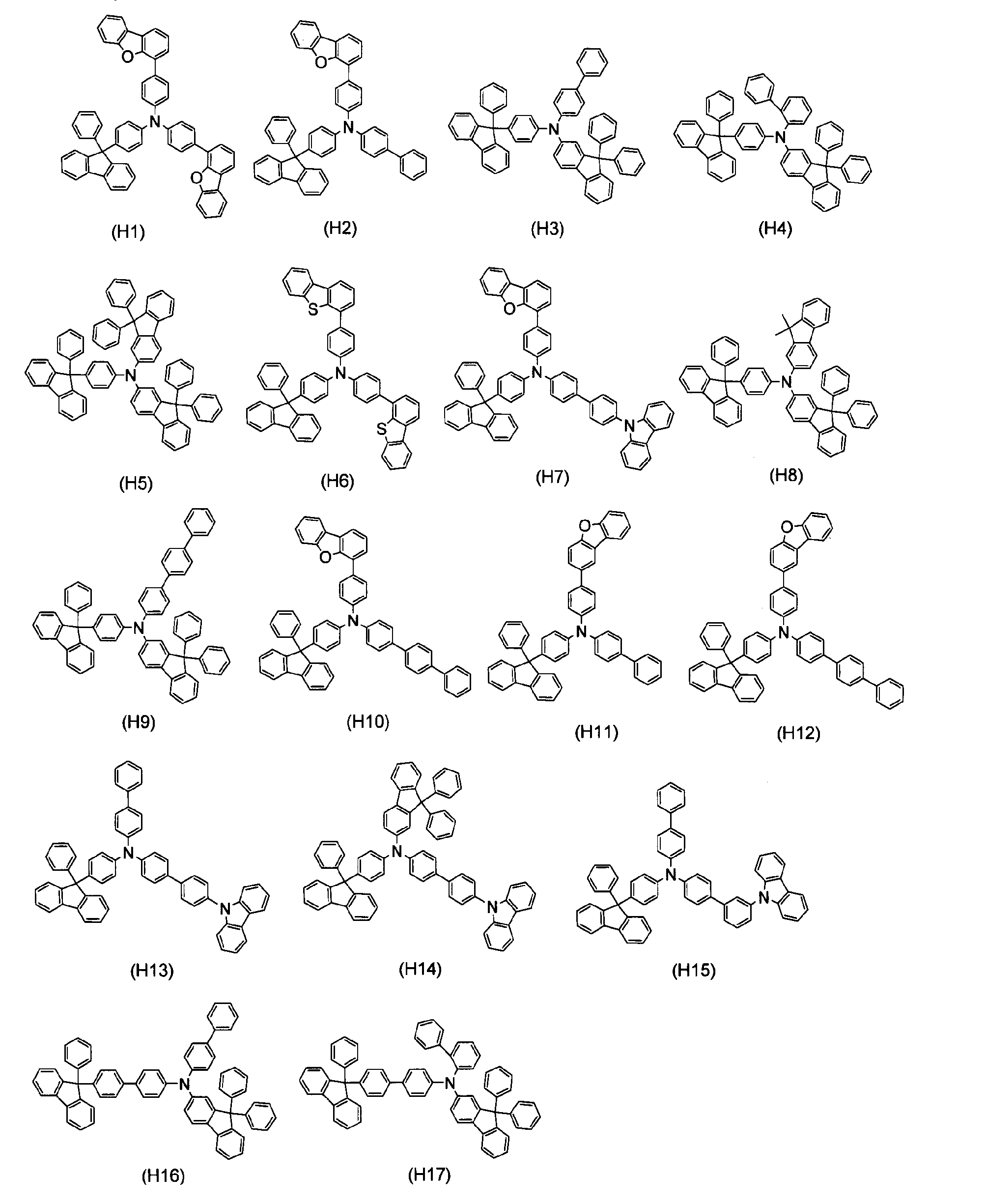
本発明の一態様の有機EL素子用材料は、上述の前記化合物(1)からなるものであり、前記化合物(1-1)~(1-7)、(1-4-1)、(1-5-1)、(1-6-1)、(1-7-1)及び(1-7-2)から選ばれる化合物からなるものであることが好ましい。
なお、以下の化合物(1)に関する記載は、化合物(1-1)~(1-7)、(1-4-1)、(1-5-1)、(1-6-1)、(1-7-1)及び(1-7-2)に置き換えて読むことができる。
本発明の一態様の有機EL素子用材料は、有機EL素子における材料として有用であり、例えば、有機EL素子の陽極と陰極との間に配置された一層以上の有機薄膜層の材料として有用であり、特に、正孔輸送層の材料又は正孔注入層の材料としてより有用である。
次に、本発明の一態様の有機EL素子について説明する。
有機EL素子の代表的な素子構成としては、以下の(1)~(13)を挙げることができるが、特にこれらに限定されるものではない。なお、(8)の素子構成が好ましく用いられる。
(1)陽極/発光層/陰極
(2)陽極/正孔注入層/発光層/陰極
(3)陽極/発光層/電子注入層/陰極
(4)陽極/正孔注入層/発光層/電子注入層/陰極
(5)陽極/有機半導体層/発光層/陰極
(6)陽極/有機半導体層/電子障壁層/発光層/陰極
(7)陽極/有機半導体層/発光層/付着改善層/陰極
(8)陽極/正孔注入層/正孔輸送層/発光層/(電子輸送層/)電子注入層/陰極
(9)陽極/絶縁層/発光層/絶縁層/陰極
(10)陽極/無機半導体層/絶縁層/発光層/絶縁層/陰極
(11)陽極/有機半導体層/絶縁層/発光層/絶縁層/陰極
(12)陽極/絶縁層/正孔注入層/正孔輸送層/発光層/絶縁層/陰極
(13)陽極/絶縁層/正孔注入層/正孔輸送層/発光層/(電子輸送層/)電子注入層/陰極
有機EL素子1は、基板2、陽極3、陰極4、及び該陽極3と陰極4との間に配置された発光ユニット10とを有する。発光ユニット10は、ホスト材料とドーパント(発光材料)を含む発光層5を有する。発光層5と陽極3との間に正孔注入・輸送層6等、発光層5と陰極4との間に電子注入・輸送層7等を形成してもよい。また、発光層5の陽極3側に電子障壁層を、発光層5の陰極4側に正孔障壁層を、それぞれ設けてもよい。これにより、電子や正孔を発光層5に閉じ込めて、発光層5における励起子の生成確率を高めることができる。
前記化合物(1)は、有機EL素子のいずれの有機薄膜層に用いてもよいが、より低電圧での駆動の観点から、正孔注入層又は正孔輸送層に用いることが好ましく、正孔輸送層に用いることがより好ましい。
つまり、本発明の一態様の有機EL素子としては、前記一層以上の有機薄膜層が、前記化合物(1)を含む正孔注入層及び前記化合物(1)を含む正孔輸送層の少なくとも一方を含む有機EL素子であることがより好ましい。
基板は、発光素子の支持体として用いられる。基板としては、例えば、ガラス、石英、プラスチック等を用いることができる。また、可撓性基板を用いてもよい。可撓性基板とは、折り曲げることができる(フレキシブル)基板のことであり、例えば、ポリカーボネート、ポリアリレート、ポリエーテルスルフォン、ポリプロピレン、ポリエステル、ポリフッ化ビニル、ポリ塩化ビニルからなるプラスチック基板等が挙げられる。また、無機蒸着フィルムを用いることもできる。
基板上に形成される陽極には、仕事関数の大きい(具体的には4.0eV以上)金属、合金、電気伝導性化合物、及びこれらの混合物等を用いることが好ましい。具体的には、例えば、酸化インジウム-酸化スズ(ITO:Indium Tin Oxide)、珪素もしくは酸化珪素を含有した酸化インジウム-酸化スズ、酸化インジウム-酸化亜鉛、酸化タングステン、及び酸化亜鉛を含有した酸化インジウム、グラフェン等が挙げられる。この他、金(Au)、白金(Pt)、ニッケル(Ni)、タングステン(W)、クロム(Cr)、モリブデン(Mo)、鉄(Fe)、コバルト(Co)、銅(Cu)、パラジウム(Pd)、チタン(Ti)、又は金属材料の窒化物(例えば、窒化チタン)等が挙げられる。
仕事関数の小さい材料である、元素周期表の第1族又は第2族に属する元素、すなわちリチウム(Li)やセシウム(Cs)等のアルカリ金属、及びマグネシウム(Mg)、カルシウム(Ca)、ストロンチウム(Sr)等のアルカリ土類金属、及びこれらを含む合金(例えば、MgAg、AlLi)、ユーロピウム(Eu)、イッテルビウム(Yb)等の希土類金属及びこれらを含む合金等を用いることもできる。なお、アルカリ金属、アルカリ土類金属、及びこれらを含む合金を用いて陽極を形成する場合には、真空蒸着法やスパッタリング法を用いることができる。さらに、銀ペースト等を用いる場合には、塗布法やインクジェット法等を用いることができる。
正孔注入層は、正孔注入性の高い物質を含む層である。
本発明の一態様の有機EL素子の当該正孔注入層は、本発明の一態様の前記化合物(1)を単独で又は下記の化合物と組み合わせて含むことが好ましい。
正孔輸送層は、正孔輸送性の高い物質を含む層である。
本発明の一態様の有機EL素子の当該正孔輸送層は、本発明の一態様の前記化合物(1)を単独で又は下記の化合物と組み合わせて含むことが好ましい。
但し、電子よりも正孔の輸送性の高い物質であれば、これら以外のものを用いてもよい。なお、正孔輸送性の高い物質を含む層は、単層のものだけでなく、上記物質からなる層が二層以上積層したものとしてもよい。例えば、正孔輸送層は第1正孔輸送層(陽極側)と第2正孔輸送層(発光層側)の2層構造にしてもよい。この場合、本発明の一態様の前記化合物(1)は第1正孔輸送層と第2正孔輸送層のいずれに含まれていてもよいが、第2正孔輸送層に含まれていることが好ましい。
受容性化合物としては、下記式(EA)で表される化合物が好ましい。
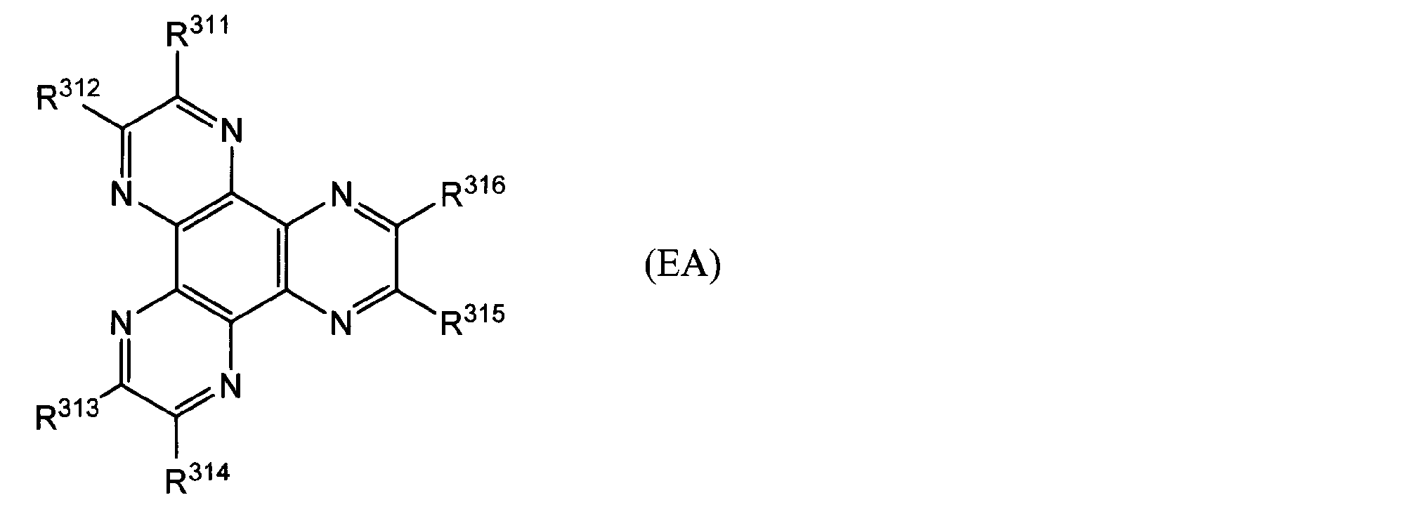
R317で表されるアルキル基としては、例えば、メチル基、エチル基、n-プロピル基、イソプロピル基、n-ブチル基、イソブチル基、t-ブチル基等が挙げられ、シクロアルキル基としては、例えば、シクロペンチル基、シクロヘキシル基等が挙げられる。
受容性化合物を含有する層の膜厚は、特に限定されないが、好ましくは5~20nmである。
発光層は、発光性の高い物質を含む層であり、種々の材料を用いることができる。例えば、発光性の高い物質としては、蛍光を発光する蛍光性化合物や燐光を発光する燐光性化合物を用いることができる。蛍光性化合物は一重項励起状態から発光可能な化合物であり、燐光性化合物は三重項励起状態から発光可能な化合物である。
発光層に用いることができる青色系の蛍光発光材料として、ピレン誘導体、スチリルアミン誘導体、クリセン誘導体、フルオランテン誘導体、フルオレン誘導体、ジアミン誘導体、トリアリールアミン誘導体等が使用できる。具体的には、N,N’-ビス[4-(9H-カルバゾール-9-イル)フェニル]-N,N’-ジフェニルスチルベン-4,4’-ジアミン(略称:YGA2S)、4-(9H-カルバゾール-9-イル)-4’-(10-フェニル-9-アントリル)トリフェニルアミン(略称:YGAPA)、4-(10-フェニル-9-アントリル)-4’-(9-フェニル-9H-カルバゾール-3-イル)トリフェニルアミン(略称:PCBAPA)等が挙げられる。
発光層としては、上述した発光性の高い物質(ゲスト材料)を他の物質(ホスト材料)に分散させた構成としてもよい。発光性の高い物質を分散させるための物質としては、各種のものを用いることができ、発光性の高い物質よりも最低空軌道準位(LUMO準位)が高く、最高占有分子軌道準位(HOMO準位)が低い物質を用いることが好ましい。
(1)アルミニウム錯体、ベリリウム錯体、もしくは亜鉛錯体等の金属錯体、
(2)オキサジアゾール誘導体、ベンゾイミダゾール誘導体、もしくはフェナントロリン誘導体等の複素環化合物、
(3)カルバゾール誘導体、アントラセン誘導体、フェナントレン誘導体、ピレン誘導体、もしくはクリセン誘導体等の縮合芳香族化合物、
(4)トリアリールアミン誘導体、もしくは縮合多環芳香族アミン誘導体等の芳香族アミン化合物が使用される。
具体的には、トリス(8-キノリノラト)アルミニウム(III)(略称:Alq)、トリス(4-メチル-8-キノリノラト)アルミニウム(III)(略称:Almq3)、ビス(10-ヒドロキシベンゾ[h]キノリナト)ベリリウム(II)(略称:BeBq2)、ビス(2-メチル-8-キノリノラト)(4-フェニルフェノラト)アルミニウム(III)(略称:BAlq)、ビス(8-キノリノラト)亜鉛(II)(略称:Znq)、ビス[2-(2-ベンゾオキサゾリル)フェノラト]亜鉛(II)(略称:ZnPBO)、ビス[2-(2-ベンゾチアゾリル)フェノラト]亜鉛(II)(略称:ZnBTZ)等の金属錯体、2-(4-ビフェニリル)-5-(4-tert-ブチルフェニル)-1,3,4-オキサジアゾール(略称:PBD)、1,3-ビス[5-(p-tert-ブチルフェニル)-1,3,4-オキサジアゾール-2-イル]ベンゼン(略称:OXD-7)、3-(4-ビフェニリル)-4-フェニル-5-(4-tert-ブチルフェニル)-1,2,4-トリアゾール(略称:TAZ)、2,2’,2’’-(1,3,5-ベンゼントリイル)トリス(1-フェニル-1H-ベンゾイミダゾール)(略称:TPBI)、バソフェナントロリン(略称:BPhen)、バソキュプロイン(略称:BCP)等の複素環化合物や、9-[4-(10-フェニル-9-アントリル)フェニル]-9H-カルバゾール(略称:CzPA)、3,6-ジフェニル-9-[4-(10-フェニル-9-アントリル)フェニル]-9H-カルバゾール(略称:DPCzPA)、9,10-ビス(3,5-ジフェニルフェニル)アントラセン(略称:DPPA)、9,10-ジ(2-ナフチル)アントラセン(略称:DNA)、2-tert-ブチル-9,10-ジ(2-ナフチル)アントラセン(略称:t-BuDNA)、9,9’-ビアントリル(略称:BANT)、9,9’-(スチルベン-3,3’-ジイル)ジフェナントレン(略称:DPNS)、9,9’-(スチルベン-4,4’-ジイル)ジフェナントレン(略称:DPNS2)、3,3’,3’’-(ベンゼン-1,3,5-トリイル)トリピレン(略称:TPB3)、9,10-ジフェニルアントラセン(略称:DPAnth)、6,12-ジメトキシ-5,11-ジフェニルクリセン等の縮合芳香族化合物、N,N-ジフェニル-9-[4-(10-フェニル-9-アントリル)フェニル]-9H-カルバゾール-3-アミン(略称:CzA1PA)、4-(10-フェニル-9-アントリル)トリフェニルアミン(略称:DPhPA)、N,9-ジフェニル-N-[4-(10-フェニル-9-アントリル)フェニル]-9H-カルバゾール-3-アミン(略称:PCAPA)、N,9-ジフェニル-N-{4-[4-(10-フェニル-9-アントリル)フェニル]フェニル}-9H-カルバゾール-3-アミン(略称:PCAPBA)、N-(9,10-ジフェニル-2-アントリル)-N,9-ジフェニル-9H-カルバゾール-3-アミン(略称:2PCAPA)、NPB(又はα-NPD)、TPD、DFLDPBi、BSPB等の芳香族アミン化合物等を用いることができる。また、発光性の高い物質(ゲスト材料)を分散させるための物質(ホスト材料)は複数種用いることができる。
電子輸送層は、電子輸送性の高い物質を含む層である。電子輸送層には、
(1)アルミニウム錯体、ベリリウム錯体、亜鉛錯体等の金属錯体、
(2)イミダゾール誘導体、ベンゾイミダゾール誘導体、アジン誘導体、カルバゾール誘導体、フェナントロリン誘導体等の複素芳香族化合物、
(3)高分子化合物を使用することができる。
具体的には低分子の有機化合物として、Alq、トリス(4-メチル-8-キノリノラト)アルミニウム(略称:Almq3)、ビス(10-ヒドロキシベンゾ[h]キノリナト)ベリリウム(略称:BeBq2)、BAlq、Znq、ZnPBO、ZnBTZ等の金属錯体等を用いることができる。また、金属錯体以外にも、2-(4-ビフェニリル)-5-(4-tert-ブチルフェニル)-1,3,4-オキサジアゾール(略称:PBD)、1,3-ビス[5-(ptert-ブチルフェニル)-1,3,4-オキサジアゾール-2-イル]ベンゼン(略称:OXD-7)、3-(4-tert-ブチルフェニル)-4-フェニル-5-(4-ビフェニリル)-1,2,4-トリアゾール(略称:TAZ)、3-(4-tert-ブチルフェニル)-4-(4-エチルフェニル)-5-(4-ビフェニリル)-1,2,4-トリアゾール(略称:p-EtTAZ)、バソフェナントロリン(略称:BPhen)、バソキュプロイン(略称:BCP)、4,4’-ビス(5-メチルベンゾオキサゾール-2-イル)スチルベン(略称:BzOs)等の複素芳香族化合物も用いることができる。ここに述べた物質は、主に10-6cm2/Vs以上の電子移動度を有する物質である。なお、正孔輸送性よりも電子輸送性の高い物質であれば、上記以外の物質を電子輸送層として用いてもよい。また、電子輸送層は、単層のものだけでなく、上記物質からなる層が二層以上積層したものとしてもよい。
また、電子輸送層には、高分子化合物を用いることもできる。例えば、ポリ[(9,9-ジヘキシルフルオレン-2,7-ジイル)-co-(ピリジン-3,5-ジイル)](略称:PF-Py)、ポリ[(9,9-ジオクチルフルオレン-2,7-ジイル)-co-(2,2’-ビピリジン-6,6’-ジイル)](略称:PF-BPy)等を用いることができる。
電子注入層は、電子注入性の高い物質を含む層である。電子注入層には、リチウム(Li)、セシウム(Cs)、カルシウム(Ca)、フッ化リチウム(LiF)、フッ化セシウム(CsF)、フッ化カルシウム(CaF2)、リチウム酸化物(LiOx)等のようなアルカリ金属、アルカリ土類金属、又はそれらの化合物を用いることができる。その他、電子輸送性を有する物質にアルカリ金属、アルカリ土類金属、又はそれらの化合物を含有させたもの、具体的にはAlq中にマグネシウム(Mg)を含有させたもの等を用いてもよい。なお、この場合には、陰極からの電子注入をより効率良く行うことができる。
あるいは、電子注入層に、有機化合物と電子供与体(ドナー)とを混合してなる複合材料を用いてもよい。このような複合材料は、電子供与体によって有機化合物に電子が発生するため、電子注入性及び電子輸送性に優れている。この場合、有機化合物としては、発生した電子の輸送に優れた材料であることが好ましく、具体的には、例えば上述した電子輸送層を構成する物質(金属錯体や複素芳香族化合物等)を用いることができる。電子供与体としては、有機化合物に対し電子供与性を示す物質であればよい。具体的には、アルカリ金属やアルカリ土類金属や希土類金属が好ましく、リチウム、セシウム、マグネシウム、カルシウム、エルビウム、イッテルビウム等が挙げられる。また、アルカリ金属酸化物やアルカリ土類金属酸化物が好ましく、リチウム酸化物、カルシウム酸化物、バリウム酸化物等が挙げられる。また、酸化マグネシウムのようなルイス塩基を用いることもできる。また、テトラチアフルバレン(略称:TTF)等の有機化合物を用いることもできる。
陰極には、仕事関数の小さい(具体的には3.8eV以下)金属、合金、電気伝導性化合物、及びこれらの混合物等を用いることが好ましい。このような陰極材料の具体例としては、元素周期表の第1族又は第2族に属する元素、すなわちリチウム(Li)やセシウム(Cs)等のアルカリ金属、及びマグネシウム(Mg)、カルシウム(Ca)、ストロンチウム(Sr)等のアルカリ土類金属、及びこれらを含む合金(例えば、MgAg、AlLi)、ユーロピウム(Eu)、イッテルビウム(Yb)等の希土類金属及びこれらを含む合金等が挙げられる。
なお、アルカリ金属、アルカリ土類金属、これらを含む合金を用いて陰極を形成する場合には、真空蒸着法やスパッタリング法を用いることができる。また、銀ペースト等を用いる場合には、塗布法やインクジェット法等を用いることができる。
なお、電子注入層を設けることにより、仕事関数の大小に関わらず、Al、Ag、ITO、グラフェン、珪素もしくは酸化珪素を含有した酸化インジウム-酸化スズ等様々な導電性材料を用いて陰極を形成することができる。これらの導電性材料は、スパッタリング法やインクジェット法、スピンコート法等を用いて成膜することができる。
また、正孔輸送層の膜厚は、好ましくは10nm~300nmである。
なお、正孔輸送層が上述のような2層構造である場合には、特に制限は無いが、第1正孔輸送層の膜厚は、好ましくは50~300nm、より好ましくは50~250nm、更に好ましくは50~200nm、より更に好ましくは50~150nmであり、第2正孔輸送層の膜厚は、好ましくは5~100nm、より好ましくは5~50nm、更に好ましくは5~30nm、より更に好ましくは5~20nmである。
本発明の一態様の電子機器は、上述の本発明の一態様の有機EL素子を搭載したものである。
このような電子機器としては、例えば、有機ELパネルモジュール等の表示部品、テレビ、携帯電話、パーソナルコンピュータ等の表示装置、及び、照明、車両用灯具の発光装置等が挙げられる。
なお、以下の合成反応を参照し、目的物に合わせた公知の代替反応や原料を用いることによって、本願の特許請求の範囲で規定の化合物を合成することが可能である。
中間体合成例1-1(中間体(1-1)の合成)
アルゴン雰囲気下、4-ヨードブロモベンゼンを28.3g(100.0mmol)、ジベンゾフラン-4-ボロン酸を22.3g(105.0mmol)、Pd[PPh3]4を2.31g(2.00mmol)それぞれ秤量し、トルエン150ml、ジメトキシエタン150ml、及び2MのNa2CO3水溶液150ml(300.0mmol)を加え、10時間加熱還流攪拌した。
反応終了後、室温まで冷却し、反応混合物を分液ロートに移し、ジクロロメタンを用いて抽出した。有機層をMgSO4で乾燥後、ろ過、濃縮した。濃縮残渣をシリカゲルカラムクロマトグラフィーにて精製し、26.2gの白色固体(収率81%)を得た。
FD-MSの分析(電界脱離質量分析)により、当該白色固体を下記中間体(1-1)と同定した。

アルゴン雰囲気下、4’-ブロモアセトアニリドを24.0g(112.0mmol)、ジベンゾフラン-4-ボロン酸を28.6g(135.0mmol)、Pd[PPh3]4を2.6g(2.24mmol)それぞれ秤量し、トルエン450ml、ジメトキシエタン100ml、2MのNa2CO3水溶液110ml(220.0mmol)を加え、10時間加熱還流攪拌した。
反応終了後、室温まで冷却し、析出した結晶をろ過した。得られた結晶をテトラヒドロフランに溶解させ、セライト/シリカゲルを通して濾過し、濾液を減圧下で濃縮した。得られた残渣をメタノール/ヘキサンで洗浄、乾燥し、18.0gの白色固体(収率53%)を得た。
FD-MSの分析により、当該白色固体を下記中間体(1-2)と同定した。
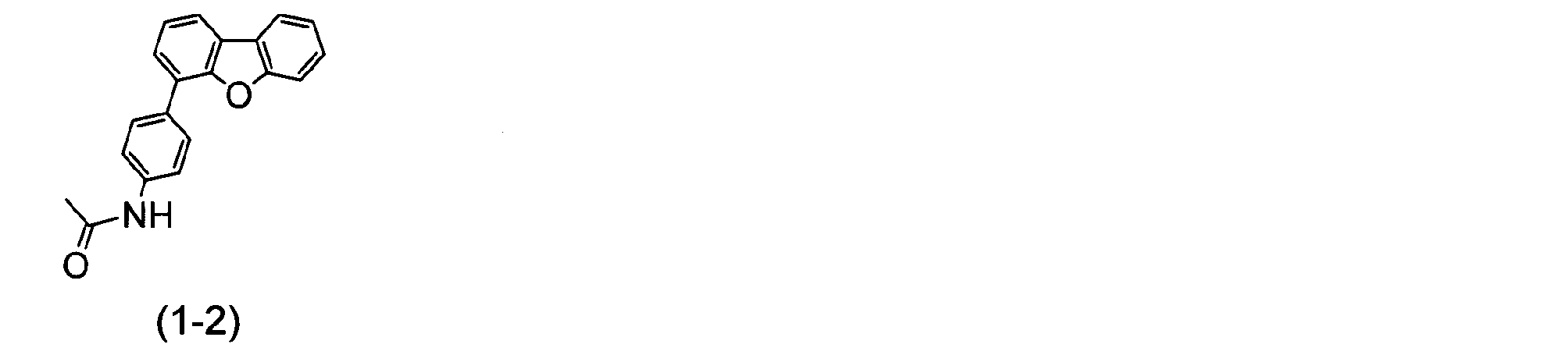
中間体(1-2)を18.0g(59.7mmol)秤量し、キシレン120ml、水1200ml、エタノール60mlを加え、攪拌した。さらに、水酸化カリウム20.0g(360.0mmol)を加え、10時間加熱還流攪拌した。
反応終了後、室温まで冷却し、反応混合物を分液ロートに移し、トルエンを用いて抽出した。有機層をMgSO4で乾燥後、ろ過、濃縮した。得られた残渣をキシレンで再結晶化し、析出した結晶を濾取した後、乾燥し、14.7gの白色結晶(収率95%)を得た。
FD-MSの分析により、当該白色結晶を下記中間体(1-3)と同定した。

アルゴン雰囲気下、4-ヨードブロモベンゼンを28.3g(100.0mmol)、ジベンゾチオフェン-4-ボロン酸を23.9g(105.0mmol)、Pd[PPh3]4を2.31g(2.00mmol)それぞれ秤量し、トルエン150ml、ジメトキシエタン150ml、2MのNa2CO3水溶液150ml(300.0mmol)を加え、10時間加熱還流攪拌した。
反応終了後、室温まで冷却し、反応混合物を分液ロートに移し、ジクロロメタンを用いて抽出した。有機層をMgSO4で乾燥後、ろ過、濃縮した。濃縮残渣をシリカゲルカラムクロマトグラフィーにて精製し、27.1gの白色固体(収率80%)を得た。
FD-MSの分析により、当該白色固体を下記中間体(1-4)と同定した。

アルゴン雰囲気下、4’-ブロモアセトアニリドを24.0g(112.0mmol)、ジベンゾチオフェン-4-ボロン酸を30.8g(135.0mmol)、Pd[PPh3]4を2.6g(2.24mmol)それぞれ秤量し、トルエン450ml、ジメトキシエタン100ml、2MのNa2CO3水溶液110ml(220.0mmol)を加え、10時間加熱還流攪拌した。
反応終了後、室温まで冷却し、析出した結晶をろ過した。得られた結晶をテトラヒドロフランに溶解させ、セライト/シリカゲルを通して濾過し、濾液を減圧下で濃縮した。得られた残渣をメタノール/ヘキサンで洗浄、乾燥し、17.8gの白色固体(収率50%)を得た。
FD-MSの分析により、当該白色固体を下記中間体(1-5)と同定した。

中間体(1-5)を18.0g(56.1mmol)秤量し、キシレン120ml、水1200ml、エタノール60mlを加え、攪拌した。さらに、水酸化カリウム20.0g(360.0mmol)を加え、10時間加熱還流攪拌した。
反応終了後、室温まで冷却し、反応混合物を分液ロートに移し、トルエンを用いて抽出した。有機層をMgSO4で乾燥後、ろ過、濃縮した。得られた残渣をキシレンで再結晶化し、析出した結晶を濾取した後、乾燥し、14.7gの白色結晶(収率95%)を得た。
FD-MSの分析により、当該白色結晶を下記中間体(1-6)と同定した。

アルゴン雰囲気下、4-ブロモビフェニルを47.0g(201.6mmol)、ヨウ素を23g(90.6mmol)、過ヨウ素酸二水和物を9.4g(41.2mmol)それぞれ秤量し、水42ml、酢酸360ml、硫酸を11mlを加え、65℃で30分間撹拌した後、さらに90℃で6時間撹拌した。
反応終了後、反応混合物を氷水に注入した後、ろ過した。水で洗浄後、メタノールでさらに洗浄することにより、67.0gの白色固体(収率93%)を得た。
FD-MSの分析により、当該白色固体を下記中間体(1-7)と同定した。

アルゴン雰囲気下、中間体(1-7)を35.9g(100.0mmol)、カルバゾールを16.7g(100.0mmol)、ヨウ化銅(CuI)を0.2g(1.00mmol)、燐酸三カリウムを42.4g(210.0mmol)それぞれ秤量し、trans-1,2-シクロヘキサンジアミンを2ml、1,4-ジオキサンを300ml加え、100℃で20時間撹拌した。
反応終了後、反応混合物に水300mlを加えた後、分液し、水層を除去した。有機層を硫酸ナトリウムで乾燥させた後、濃縮した。残渣をシリカゲルカラムクロマトグラフィーで精製し、23.1gの白色固体(収率58%)を得た。
FD-MSの分析により、当該白色固体を下記中間体(1-8)と同定した。

アルゴン雰囲気下、4-ヨードブロモベンゼンを28.3g(100.0mmol)、ジベンゾフラン-2-ボロン酸を22.3g(105.0mmol)、Pd[PPh3]4を2.31g(2.00mmol)それぞれ秤量し、トルエン150ml、ジメトキシエタン150ml、及び2MのNa2CO3水溶液150ml(300.0mmol)を加え、10時間加熱還流攪拌した。
反応終了後、室温まで冷却し、反応混合物を分液ロートに移し、ジクロロメタンにて抽出した。有機層をMgSO4で乾燥後、ろ過、濃縮した。濃縮残渣をシリカゲルカラムクロマトグラフィーにて精製し、27.4gの白色固体(収率85%)を得た。
FD-MSの分析により、当該白色固体を下記中間体(1-9)と同定した。

アルゴン雰囲気下、4-ヨードブロモベンゼンを28.3g(100.0mmol)、3-(9H-カルバゾール-9-イル)フェニルボロン酸を30.1g(105.0mmol)、Pd[PPh3]4を2.31g(2.00mmol)それぞれ秤量し、トルエン150ml、ジメトキシエタン150ml、及び2MのNa2CO3水溶液150ml(300.0mmol)を加え、10時間加熱還流攪拌した。
反応終了後、室温まで冷却し、反応混合物を分液ロートに移し、ジクロロメタンを用いて抽出した。有機層をMgSO4で乾燥後、ろ過、濃縮した。濃縮残渣をシリカゲルカラムクロマトグラフィーにて精製し、27.2gの白色固体(収率68%)を得た。
FD-MSの分析により、当該白色固体を下記中間体(1-10)と同定した。

アルゴン雰囲気下、9-(4-ブロモフェニル)-9-フェニルフルオレンを39.7g(100.0mmol)、4-クロロフェニルボロン酸を16.4g(105.0mmol)、Pd[PPh3]4を2.31g(2.00mmol)それぞれ秤量し、トルエン150ml、ジメトキシエタン150ml、及び2MのNa2CO3水溶液150ml(300.0mmol)を加え、10時間加熱還流攪拌した。
反応終了後、室温まで冷却し、反応混合物を分液ロートに移し、ジクロロメタンにて抽出した。有機層をMgSO4で乾燥後、ろ過、濃縮した。濃縮残渣をシリカゲルカラムクロマトグラフィーにて精製し、30.0gの白色固体(収率70%)を得た。
FD-MSの分析により、当該白色固体を下記中間体(1-11)と同定した。

アルゴン雰囲気下、9-(4-ブロモフェニル)-9-フェニルフルオレンを19.9g(50.0mmol)、中間体(1-3)を13.0g(50.0mmol)、t-ブトキシナトリウムを9.6g(100.0mmol)それぞれ秤量し、脱水トルエン250mlを加え、撹拌した。さらに、酢酸パラジウム225mg(1.0mmol)、トリ-t-ブチルホスフィン202mg(1.0mmol)を加え、80℃にて8時間反応した。
冷却後、反応混合物をセライト/シリカゲルを通して濾過し、濾液を減圧下で濃縮した。得られた残渣をトルエンで再結晶化し、析出した結晶を濾取した後、乾燥し、23.0gの白色結晶(収率80%)を得た。
FD-MSの分析により、当該白色結晶を下記中間体(2-1)と同定した。
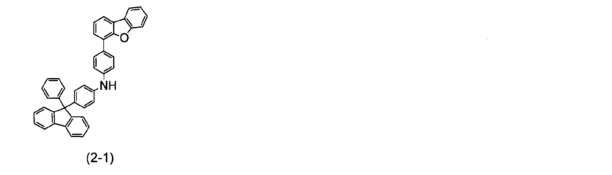
中間体合成例2-1において、中間体(1-3)の代わりに、2-アミノ-9,9’-ジフェニルフルオレンを16.7g用いた以外は、同様に反応を行ったところ、25.3gの白色結晶(収率78%)を得た。
FD-MSの分析により、当該白色結晶を下記中間体(2-2)と同定した。
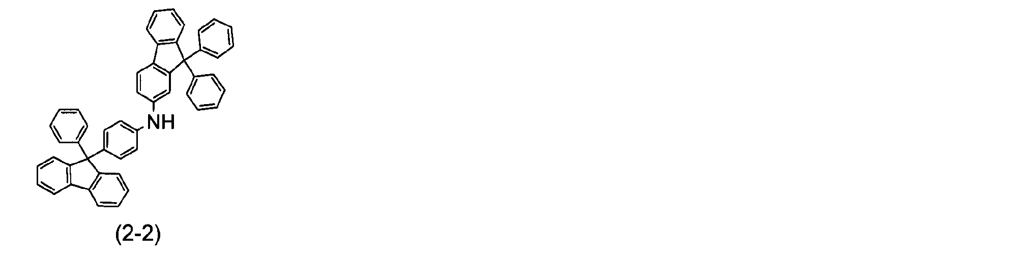
中間体合成例2-1において、中間体(1-3)の代わりに、中間体(1-6)を13.8g用いた以外は、同様に反応を行ったところ、23.7gの白色結晶(収率80%)を得た。
FD-MSの分析により、当該白色結晶を下記中間体(2-3)と同定した。
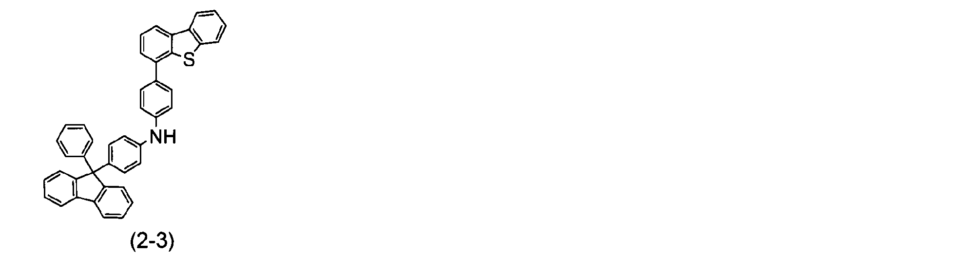
中間体合成例2-1において、中間体(1-3)の代わりに、4-アミノターフェニルを24.5g用いた以外は、同様に反応を行ったところ、22.5gの白色結晶(収率80%)を得た。
FD-MSの分析により、当該白色結晶を下記中間体(2-4)と同定した。

アルゴン雰囲気下、4-ビフェニルアセトアミドを11.4g(54.0mmol)、9-(4-ブロモフェニル)-9-フェニルフルオレンを25.8g(65.0mmol)、CuIを4.1g(21.6mmol)、N,N-ジメチルエチレンジアミンを0.95g(10.8mmol)、K3PO4を24.0g(114.0mmol)それぞれ秤量し、キシレン300mlを加え、10時間加熱還流攪拌した。
反応終了後、室温まで冷却し、セライト/シリカゲルを通して濾過し、濾液を減圧下で濃縮した。濃縮残渣をシリカゲルカラムクロマトグラフィーにて精製した後、トルエンを用いて再結晶化し、15.1gの白色結晶(収率53%)を得た。
FD-MSの分析により、当該白色結晶を下記中間体(2-5)と同定した。

中間体(2-5)を30.1g(57.0mmol)、水酸化カリウムを20.0g(352.0mmol)それぞれ秤量し、水1140ml、エタノール57ml、及びキシレン114mlを加え、10時間加熱還流攪拌した。
反応終了後、室温まで冷却し、析出した結晶をろ過し、濾別した結晶を水及びメタノールで洗浄した。一方、濾液を分液ロートに移し、トルエンを用いて抽出し、有機層をMgSO4で乾燥後、ろ過、濃縮した。得られた残渣、及び濾別した結晶を併せて、キシレンで再結晶化し、析出した結晶を濾取した後、乾燥し、24.9gの白色結晶(収率90%)を得た。
FD-MSの分析により、当該白色結晶を下記中間体(2-6)と同定した。

アルゴン雰囲気下、中間体(1-11)を21.4g(50.0mmol)、2-アミノ-9,9’-ジフェニルフルオレンを16.7g(50.0mmol)、t-ブトキシナトリウムを9.6g(100.0mmol)それぞれ秤量し、脱水トルエン250mlを加え、撹拌した。さらに、酢酸パラジウム225mg(1.0mmol)、及びトリ-t-ブチルホスフィン202mg(1.0mmol)を加え、80℃にて8時間反応した。
冷却後、反応混合物をセライト/シリカゲルを通して濾過し、濾液を減圧下で濃縮した。得られた残渣をトルエンで再結晶化し、析出した結晶を濾取した後、乾燥し、26.1gの白色結晶(収率72%)を得た。
FD-MSの分析により、当該白色結晶を下記中間体(2-7)と同定した。
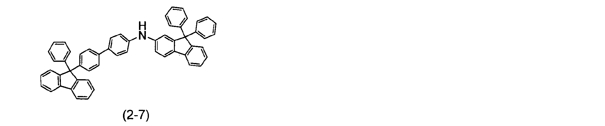
アルゴン雰囲気下、中間体(1-1)を3.2g(10.0mmol)、中間体(2-1)を5.8g(10.0mmol)、Pd2(dba)3を0.14g(0.15mmol)、P(tBu)3HBF4を0.087g(0.3mmol)、t-ブトキシナトリウムを1.9g(20.0mmol)それぞれ秤量し、無水キシレン50mlを加えて8時間加熱還流した。
反応終了後、反応混合物を50℃まで冷却し、セライト/シリカゲルを通して濾過を行い、濾液を濃縮した。得られた濃縮残渣をシリカゲルカラムクロマトグラフィーにて精製した後、トルエンを用いて再結晶化し、3.7gの白色結晶(収率45%)を得た。
FD-MSの分析により、当該白色結晶を下記化合物(H1)と同定した。
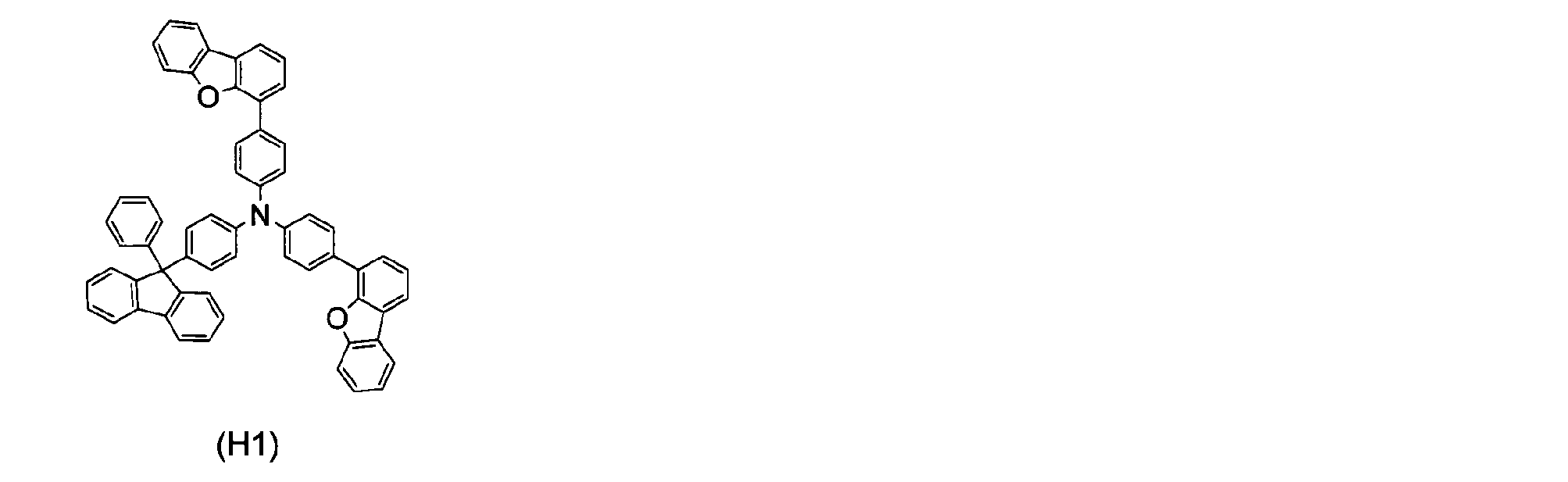
合成実施例1において、中間体(1-1)の代わりに、4-ブロモビフェニルを2.3g(10.0mmol)用いた以外は、同様に反応を行ったところ、4.0gの白色結晶(収率55%)を得た。
FD-MSの分析により、当該白色結晶を下記化合物(H2)と同定した。
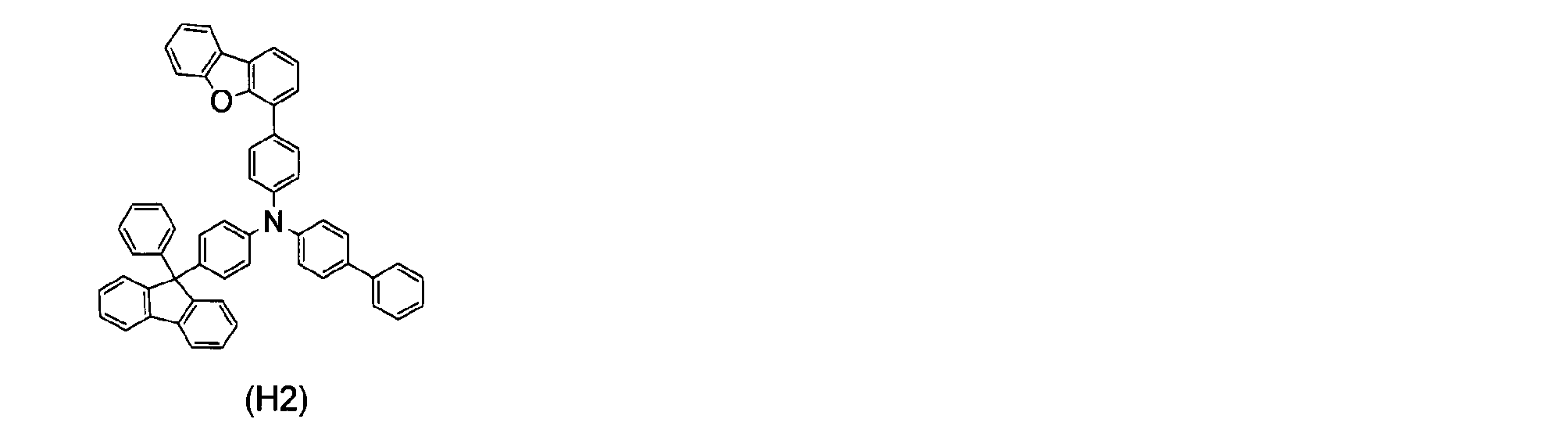
アルゴン雰囲気下、4-ブロモビフェニルを2.3g(10.0mmol)、中間体(2-2)を6.5g(10.0mmol)、Pd2(dba)3を0.14g(0.15mmol)、P(tBu)3HBF4を0.087g(0.3mmol)、t-ブトキシナトリウムを1.9g(20.0mmol)それぞれ秤量し、無水キシレン50mlを加えて8時間加熱還流した。
反応終了後、反応混合物を50℃まで冷却し、セライト/シリカゲルを通して濾過を行い、濾液を濃縮した。得られた濃縮残渣をシリカゲルカラムクロマトグラフィーにて精製した後、トルエンを用いて再結晶化し、4.4gの白色結晶(収率55%)を得た。
FD-MSの分析により、当該白色結晶を下記化合物(H3)と同定した。
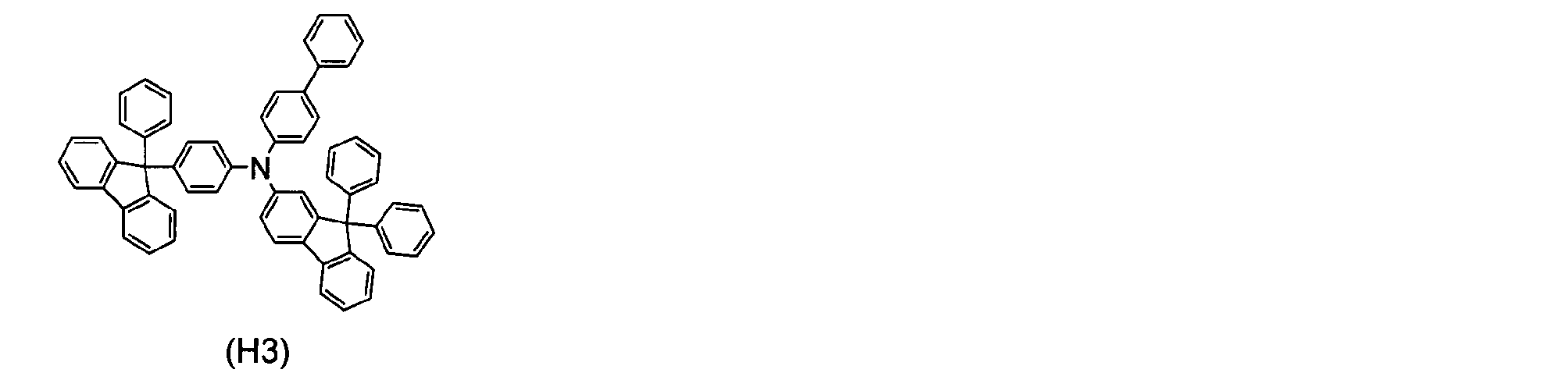
合成実施例3において、4-ブロモビフェニルの代わりに、2-ブロモビフェニルを2.3g(10.0mmol)用いた以外は、同様に反応を行ったところ、3.2gの白色結晶(収率40%)を得た。
FD-MSの分析により、当該白色結晶を下記化合物(H4)と同定した。

合成実施例3において、4-ブロモビフェニルの代わりに、2-ブロモ-9,9’-ジフェニルフルオレンを4.0g(10.0mmol)用いた以外は、同様に反応を行ったところ、4.4gの白色結晶(収率46%)を得た。
FD-MSの分析により、当該白色結晶を下記化合物(H5)と同定した。
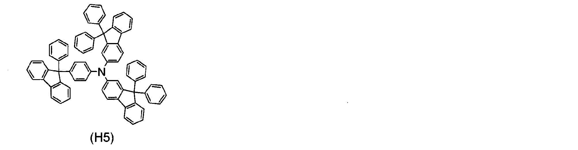
合成実施例1において、中間体(1-1)の代わりに、中間体(1-4)を3.4g(10.0mmol)用い、中間体(2-1)の代わりに、中間体(2-3)を5.9g(10.0mmol)用いた以外は、同様に反応を行ったところ、4.7gの白色結晶(収率55%)を得た。
FD-MSの分析により、当該白色結晶を化合物(H6)と同定した。
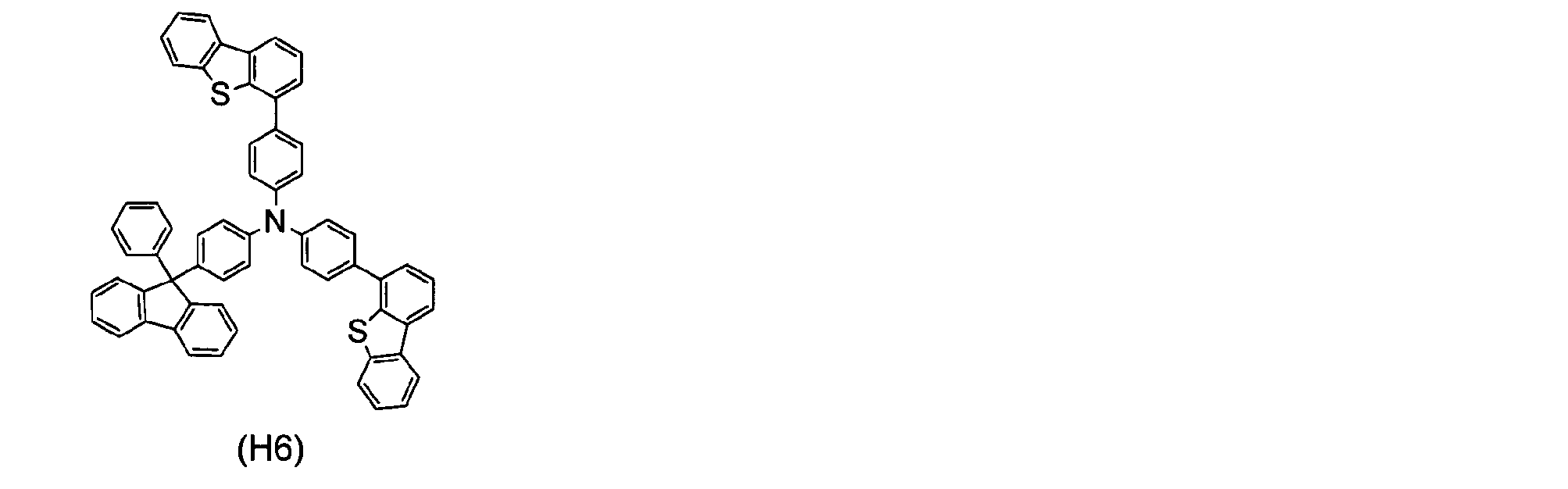
合成実施例1において、中間体(1-1)の代わりに、中間体(1-8)を4.0g(10.0mmol)用いた以外は、同様に反応を行ったところ、4.3gの白色結晶(収率50%)を得た。
FD-MSの分析により、当該白色結晶を化合物(H7)と同定した。
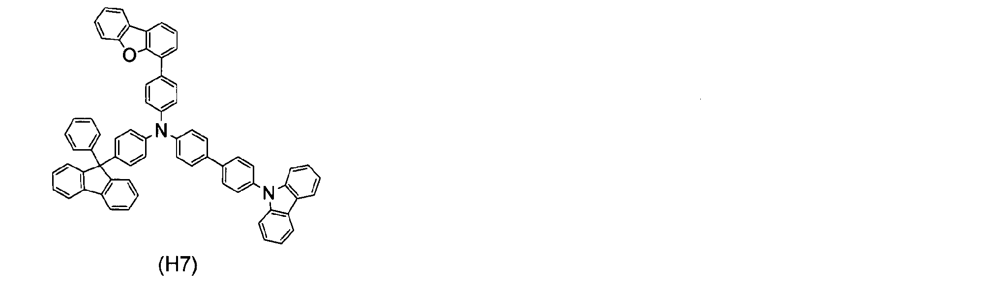
合成実施例3において、4-ブロモビフェニルの代わりに、2-ブロモ-9,9’-ジメチルフルオレンを2.7g(10.0mmol)用いた以外は、同様に反応を行ったところ、3.2gの白色結晶(収率38%)を得た。
FD-MSの分析により、当該白色結晶を下記化合物(H8)と同定した。
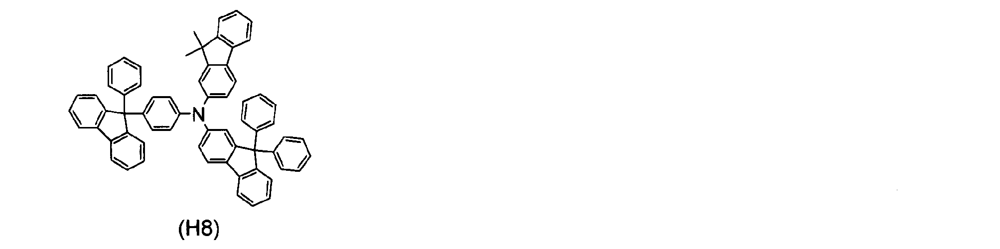
合成実施例3において、4-ブロモビフェニルの代わりに、4-ブロモ-ターフェニルを3.1g(10.0mmol)用いた以外は、同様に反応を行ったところ、3.5gの白色結晶(収率40%)を得た。
FD-MSの分析により、当該白色結晶を下記化合物(H9)と同定した。

合成実施例1において、中間体(1-1)の代わりに、4-ブロモ-ターフェニルを3.1g(10.0mmol)用いた以外は、同様に反応を行ったところ、3.2gの白色結晶(収率40%)を得た。
FD-MSの分析により、当該白色結晶を下記化合物(H10)と同定した。

合成実施例1において、中間体(1-1)の代わりに、中間体(1-9)を3.2g(10.0mmol)用い、中間体(2-1)の代わりに、中間体(2-6)を4.9g(10.0mmol)用いた以外は、同様に反応を行ったところ、2.5gの白色結晶(収率35%)を得た。
FD-MSの分析により、当該白色結晶を下記化合物(H11)と同定した。

合成実施例1において、中間体(1-1)の代わりに、中間体(1-9)を3.2g(10.0mmol)用い、中間体(2-1)の代わりに、中間体(2-4)を5.6g(10.0mmol)用いた以外は、同様に反応を行ったところ、3.5gの白色結晶(収率43%)を得た。
FD-MSの分析により、当該白色結晶を下記化合物(H12)と同定した。

合成実施例1において、中間体(1-1)の代わりに、中間体(1-8)を4.0g(10.0mmol)用い、中間体(2-1)の代わりに、中間体(2-6)を4.9g(10.0mmol)用いた以外は、同様に反応を行ったところ、3.5gの白色結晶(収率43%)を得た。
FD-MSの分析により、当該白色結晶を下記化合物(H13)と同定した。

合成実施例3において、4-ブロモビフェニルの代わりに、中間体(1-8)を4.0g(10.0mmol)用いた以外は、同様に反応を行ったところ、3.8gの白色結晶(収率39%)を得た。
FD-MSの分析により、当該白色結晶を下記化合物(H14)と同定した。

合成実施例1において、中間体(1-1)の代わりに、中間体(1-10)を4.0g(10.0mmol)用い、中間体(2-1)の代わりに、中間体(2-6)を4.9g(10.0mmol)用いた以外は、同様に反応を行ったところ、2.4gの白色結晶(収率30%)を得た。
FD-MSの分析により、当該白色結晶を下記化合物(H15)と同定した。
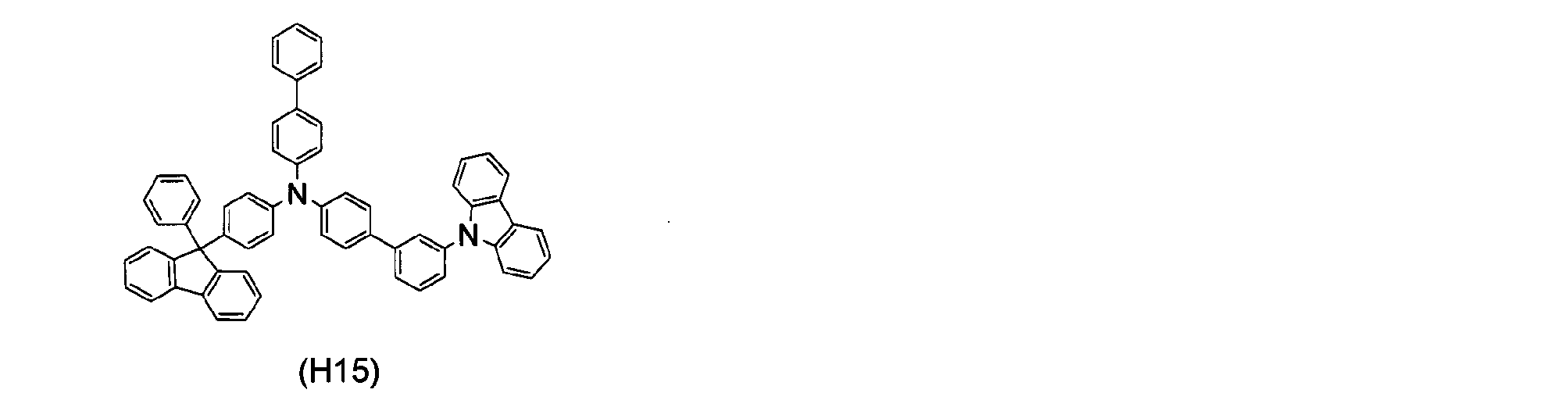
合成実施例1において、中間体(1-1)の代わりに、4-ブロモビフェニルを2.3g(10.0mmol)用い、中間体(2-1)の代わりに、中間体(2-7)を7.3g(10.0mmol)用いた以外は、同様に反応を行ったところ、2.9gの白色結晶(収率33%)を得た。
FD-MSの分析により、当該白色結晶を下記化合物(H16)と同定した。
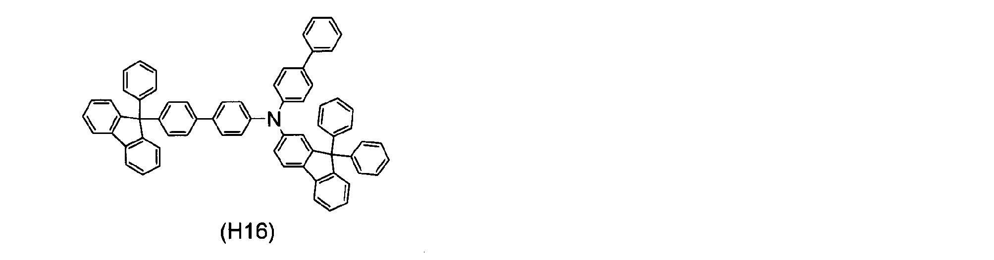
合成実施例1において、中間体(1-1)の代わりに、2-ブロモビフェニルを2.3g(10.0mmol)用い、中間体(2-1)の代わりに、中間体(2-7)を7.3g(10.0mmol)用いた以外は、同様に反応を行ったところ、2.6gの白色結晶(収率30%)を得た。
FD-MSの分析により、当該白色結晶を下記化合物(H17)と同定した。

実施例1-1~1-17(有機EL素子の作製)
25mm×75mm×1.1mmのITO透明電極ライン付きガラス基板(ジオマティック社製)をイソプロピルアルコール中で5分間超音波洗浄し、さらに、30分間UV(Ultraviolet)オゾン洗浄した。
洗浄後の透明電極ライン付きガラス基板を真空蒸着装置の基板ホルダーに装着し、まず透明電極ラインが形成されている面上に、前記透明電極を覆うようにして下記電子受容性化合物(EA1)を蒸着し、膜厚10nmの膜(EA1)を成膜した。
この膜(EA1)上に、第1正孔輸送材料として、下記芳香族アミン誘導体(X1)を蒸着し、膜厚80nmの第1正孔輸送層を成膜した。第1正孔輸送層の成膜に続けて、第2正孔輸送材料として、表1に記載の合成実施例1~17で得た上記化合物(H1)~(H17)のいずれかを蒸着し、膜厚10nmの第2正孔輸送層を成膜した。
この第2正孔輸送層上に、蛍光発光材料として、ホスト化合物(BH)とドーパント化合物(BD)とを共蒸着し、厚さ25nmの発光層を成膜した。なお、当該発光層中のドーパント化合物(BD)の濃度は4質量%であった。
続いて、この発光層上に、厚さ25nmで下記化合物(ET1)、さらに、厚さ10nmで下記化合物(ET2)、及び厚さ1nmでLiFを共蒸着し、電子輸送/注入層を成膜した。
さらに、金属Alを厚さ80nmに積層して陰極を形成し、有機EL素子を製造した。
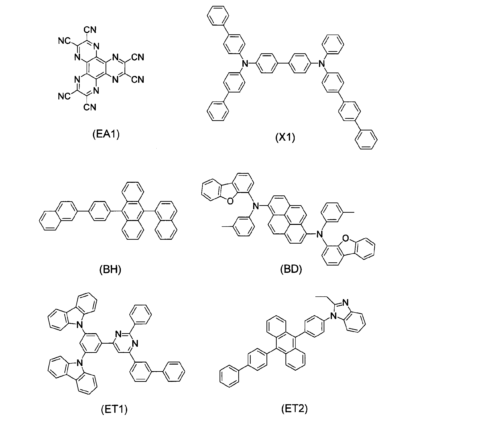
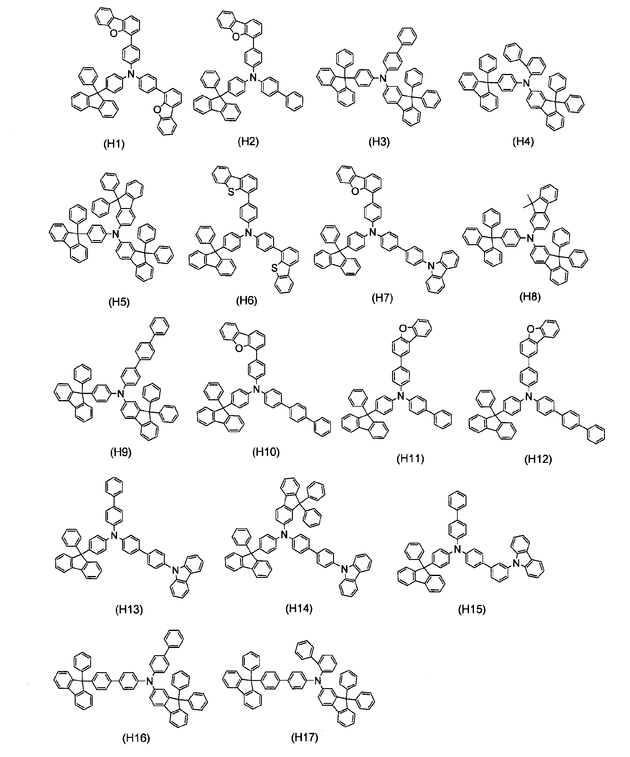
第2正孔輸送材料として、表1に記載の下記比較化合物(a1)~(a4)のいずれかを用いて第2正孔輸送層を形成した以外は、実施例1と同様にして、比較例1~4の各有機EL素子を作製した。
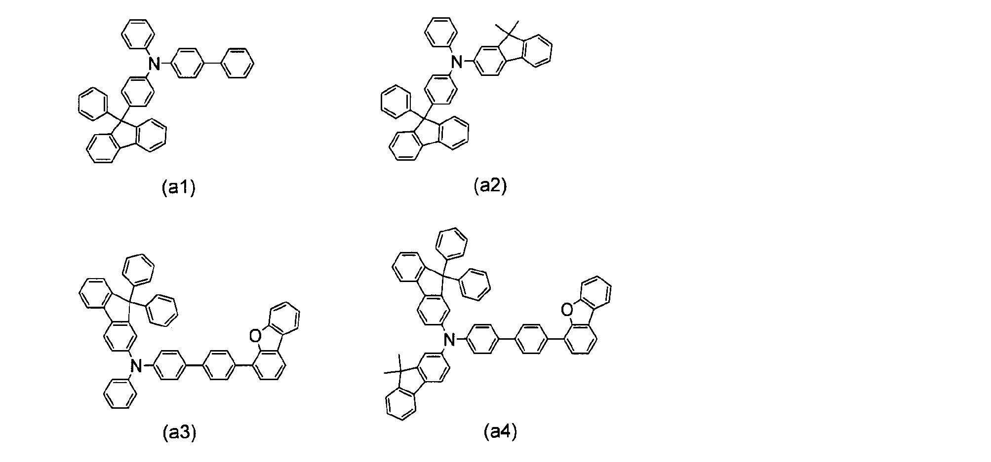
以上のようにして作製した有機EL素子を直流電流駆動により発光させ、輝度(L)、電流密度を測定し、測定結果から電流密度10mA/cm2における発光効率(cd/A)、駆動電圧(V)を求めた。さらに電流密度50mA/cm2における80%寿命を求めた。ここで、80%寿命とは、定電流駆動時において、輝度が初期輝度の80%に減衰するまでの時間をいう。結果を表1に示す。

透明電極ラインが形成されている面上に、前記透明電極を覆うようにして下記電子受容性化合物(EA2)を蒸着し、膜厚10nmの膜(EA2)を成膜し、この膜(EA1)上に、第1正孔輸送材料として、表2に記載の合成実施例3、4、5、8で得た化合物(H3)、(H4)、(H5)、(H8)のいずれかを用いて膜厚80nmの第1正孔輸送層を成膜し、当該第1の正孔輸送層上に、第2正孔輸送材料として、下記芳香族アミン誘導体(Y1)を用いて膜厚10nmの第2正孔輸送層を成膜した以外は、実施例1-1と同様にして、実施例2-1~2-4の各有機EL素子を作製した。

第1正孔輸送材料として表2に記載の前記比較化合物(a1)又は(a2)を用いて第1正孔輸送層を形成した以外は、実施例2-1と同様にして、比較例2-1~2-2の各有機EL素子を作製した。
以上のようにして作製した有機EL素子を直流電流駆動により発光させ、輝度(L)、電流密度を測定し、測定結果から電流密度10mA/cm2における電流効率(L/J)、駆動電圧(V)を求めた。さらに電流密度50mA/cm2における素子寿命を求めた。ここで、80%寿命とは、定電流駆動時において、輝度が初期輝度の80%に減衰するまでの時間をいう。結果を表2に示す。

2 基板
3 陽極
4 陰極
5 発光層
6 陽極側有機薄膜層
7 陰極側有機薄膜層
10 発光ユニット
Claims (20)
- 下記一般式(1)で表される、化合物。

m1~m3は、それぞれ独立に、0~4の整数であり、k4は、0~5の整数である。
L0~L2は、それぞれ独立に、単結合、置換もしくは無置換の環形成炭素数6~50のアリーレン基、又は置換もしくは無置換の環形成原子数5~50のヘテロアリーレン基である。
Ar1は、下記一般式(2)
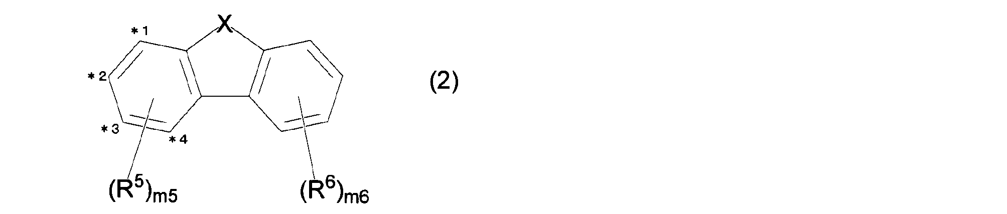
RA及びRBは、それぞれ独立に、置換もしくは無置換の環形成炭素数6~50のアリール基、置換もしくは無置換の環形成原子数5~50のヘテロアリール基を表し、RA及びRBは、同一であってもよく、互いに異っていてもよい。
R5及びR6は、それぞれ独立に、R1の規定と同じであり、m5及びm6は、それぞれ独立に、0~4の整数である。なお、R5及びR6から選ばれる2つが、互いに結合して、環構造を形成してもよい。)
で表される化合物の1価の残基であり、
上記一般式(2)中のXが-C(RA)(RB)-、-O-、及び-S-のいずれかである化合物の場合、上記一般式(2)中の*1~*4のいずれかの炭素原子と結合している水素原子又はR5が脱離し、当該炭素原子と、前記一般式(1)中のL1又は窒素原子とが結合し、
上記一般式(2)中のXが-NH-である化合物の場合、当該-NH-の窒素原子と結合している水素原子が脱離し、当該窒素原子と、前記一般式(1)中のL1又は窒素原子とが結合する。
Ar2は、置換もしくは無置換の環形成炭素数6~50のアリール基、又は置換もしくは無置換の環形成原子数5~40のヘテロアリール基である。〕 - 下記一般式(1-1)で表される、請求項1に記載の化合物。
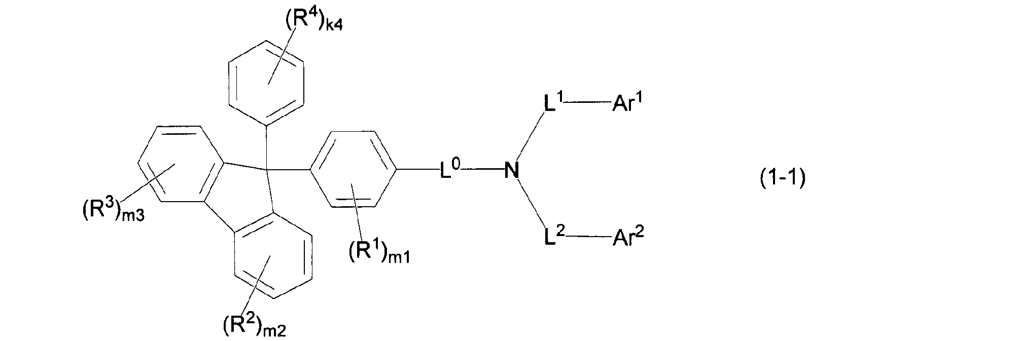
- 下記一般式(1-2)で表される、請求項1又は2に記載の化合物。

- 下記一般式(1-3)で表される、請求項1に記載の化合物。

- Ar2が、下記一般式(a)~(j)のいずれかで表される基である、請求項1~4のいずれか1項に記載の化合物。
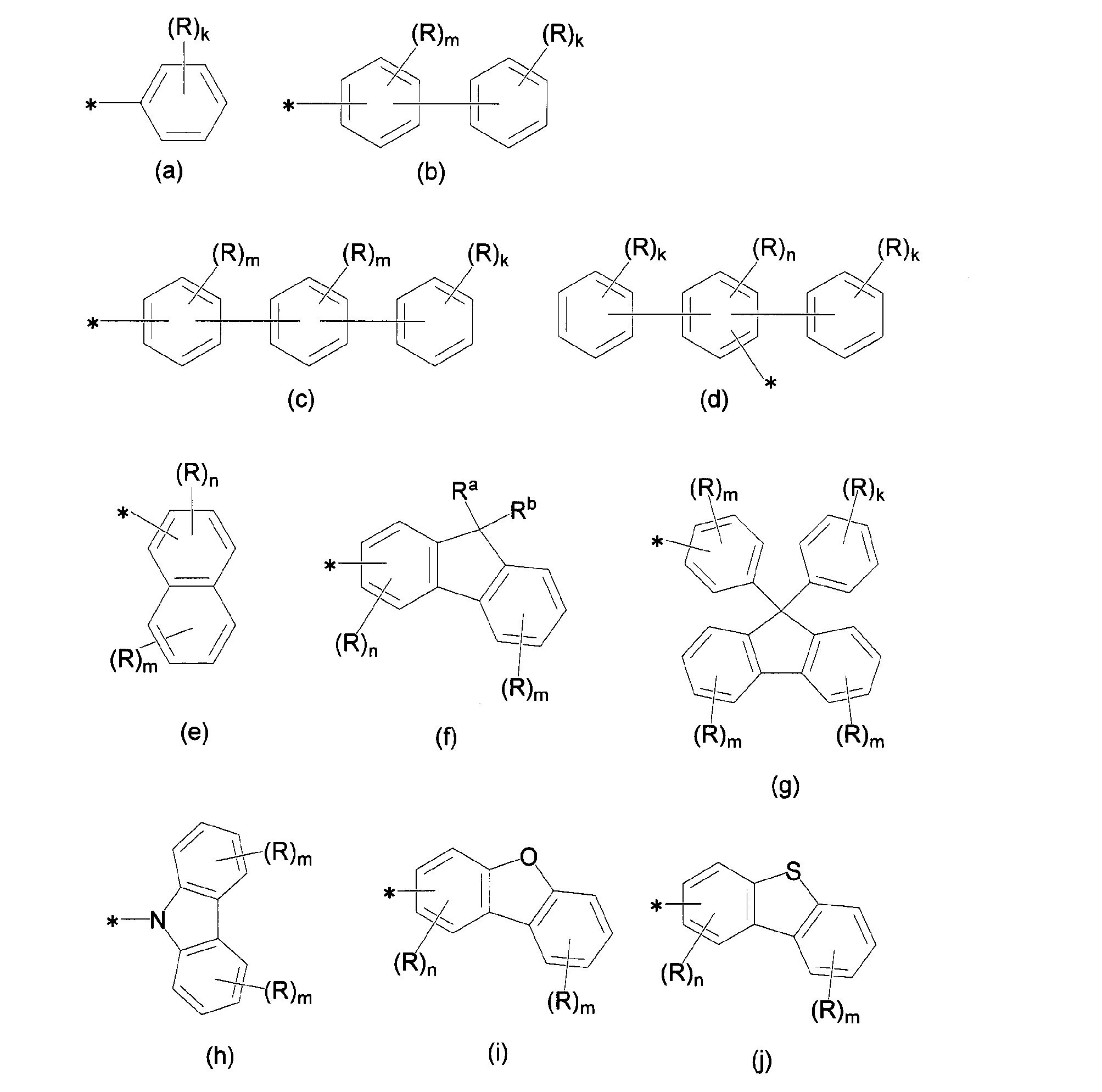
kは、それぞれ独立に、0~5の整数であり、mは、それぞれ独立に、0~4の整数であり、nは、それぞれ独立に、0~3の整数である。
*は、前記一般式(1)中のL2又は窒素原子との結合位置を示す。〕 - Ar2が、下記一般式(b-1)、(b-2)、(c-1)、(c-2)、及び(d-1)のいずれかで表される基である、請求項5に記載の化合物。
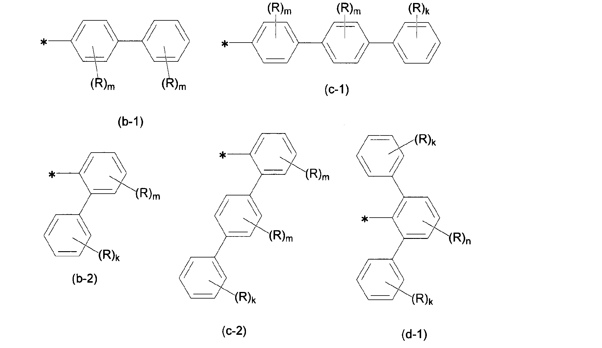
- L0~L2が、それぞれ独立に、単結合、又は下記一般式(i)及び(ii)のいずれかで表される基である、請求項1~6のいずれか1項に記載の化合物。

- 下記一般式(1-4)で表される、請求項1に記載の化合物。

- 下記一般式(1-4-1)で表される、請求項8に記載の化合物。
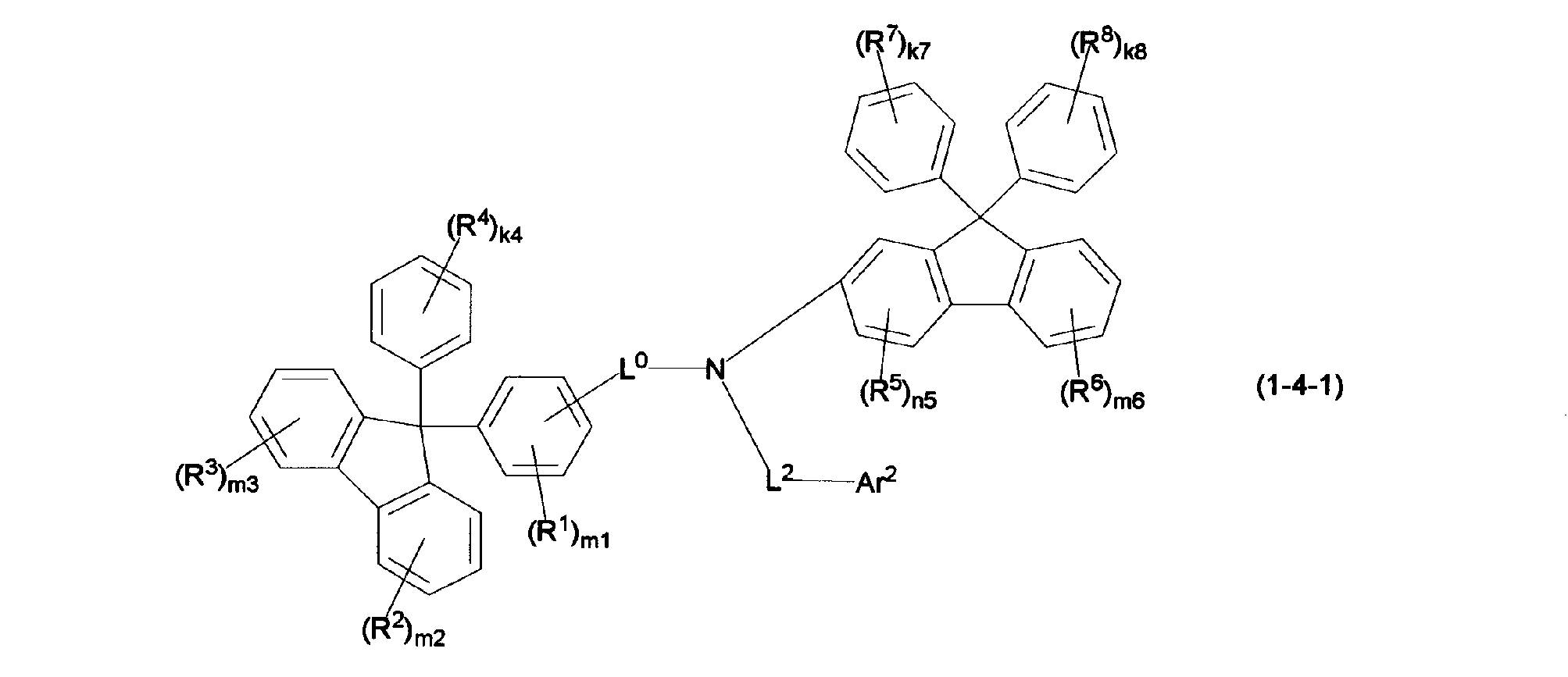
- Ar2が、下記一般式(a)~(g)のいずれかで表される基である、請求項8又は9に記載の化合物。
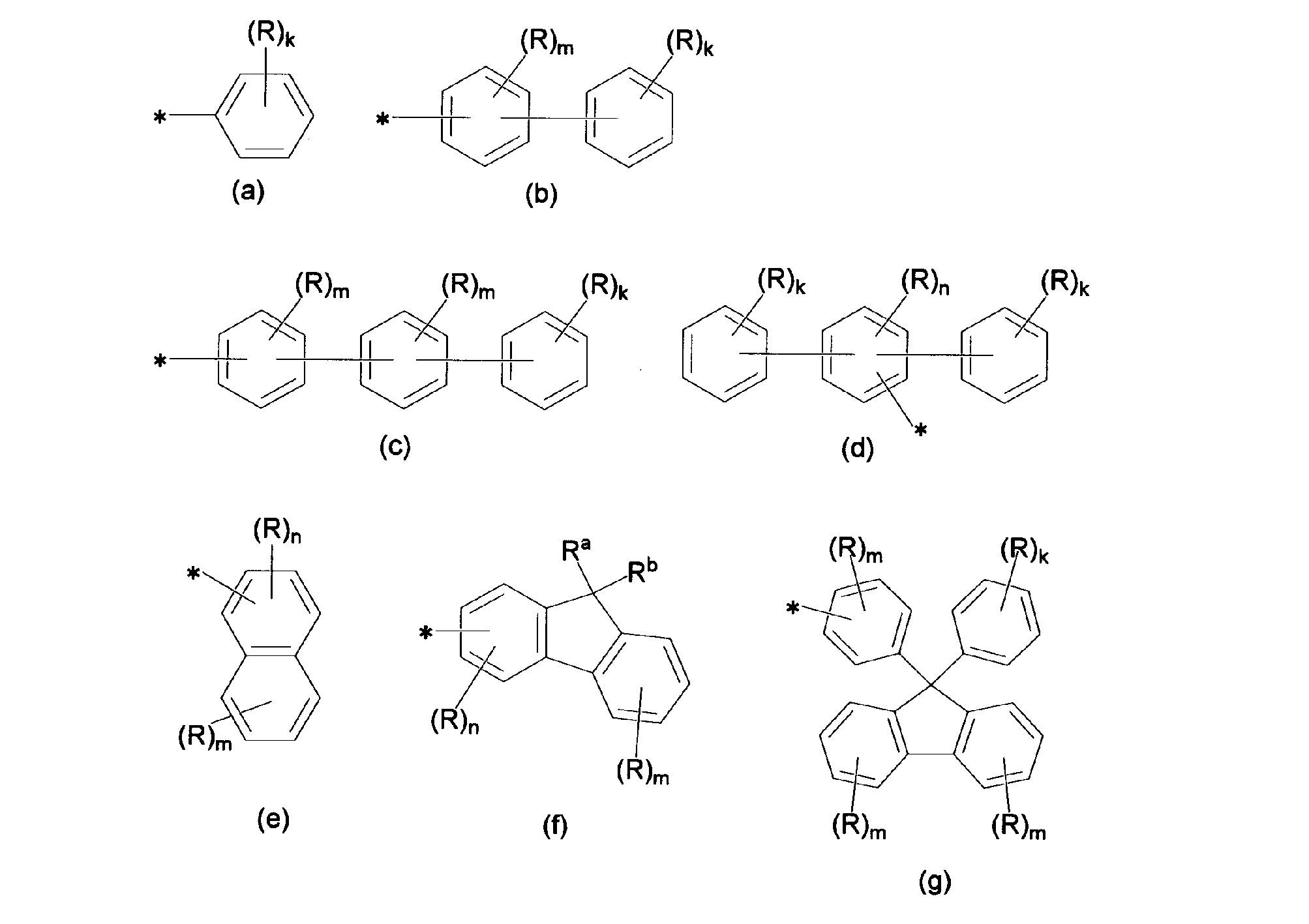
kは、それぞれ独立に、0~5の整数であり、mは、それぞれ独立に、0~4の整数であり、nは、それぞれ独立に、0~3の整数である。
*は、前記一般式(1)中のL2又は窒素原子との結合位置を示す。〕 - 下記一般式(1-5)又は(1-6)で表される、請求項1に記載の化合物。
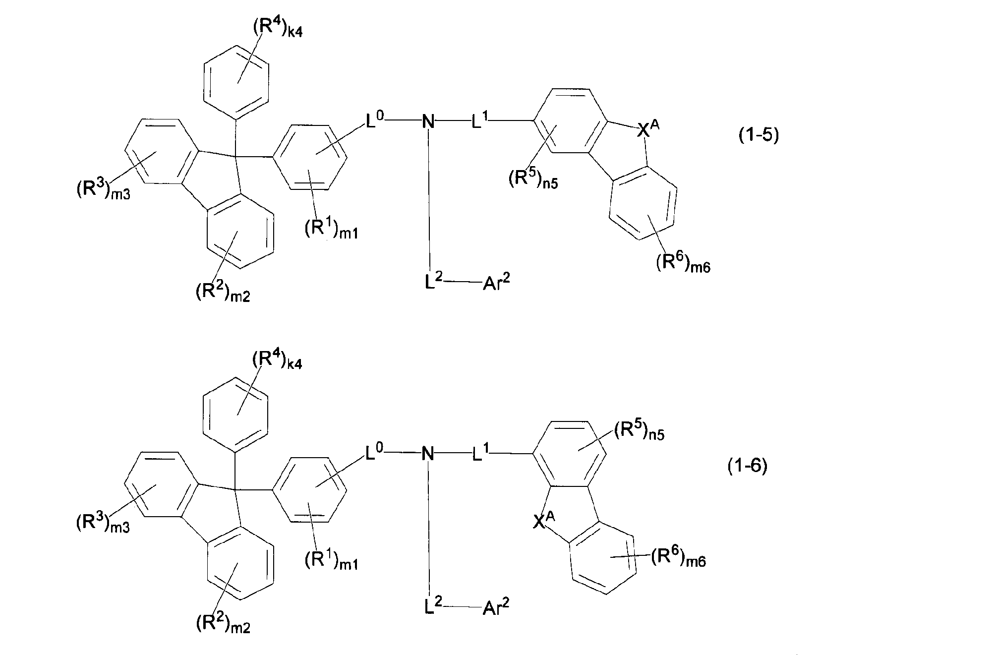
- 下記一般式(1-5-1)又は(1-6-1)で表される、請求項11に記載の化合物。
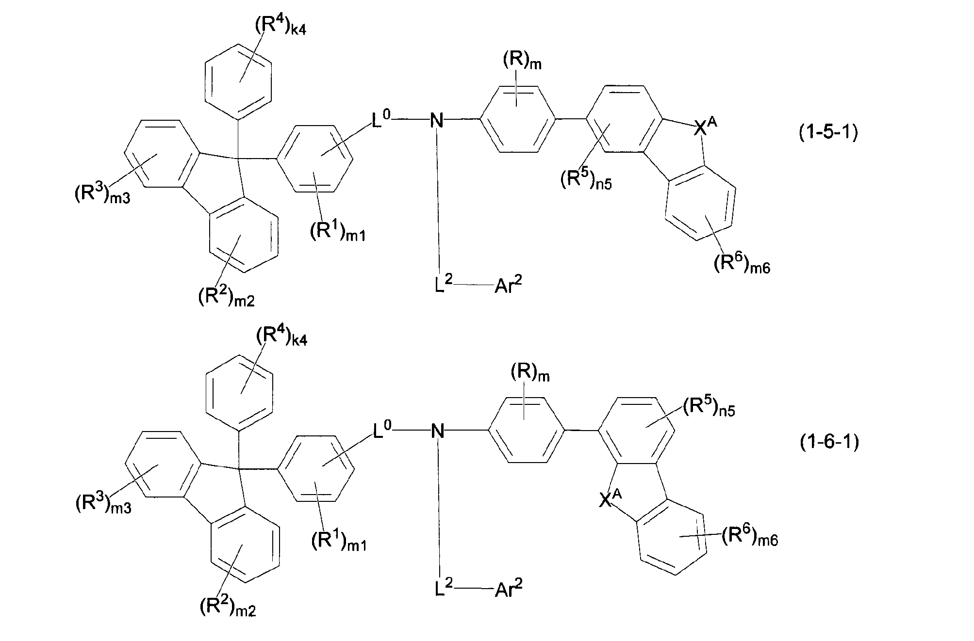
- Ar2が、下記一般式(a)~(j)のいずれかで表される基である、請求項11又は12に記載の化合物。

kは、それぞれ独立に、0~5の整数であり、mは、それぞれ独立に、0~4の整数であり、nは、それぞれ独立に、0~3の整数である。
*は、前記一般式(1)中のL2又は窒素原子との結合位置を示す。〕 - 下記一般式(1-7)で表される、請求項1に記載の化合物。
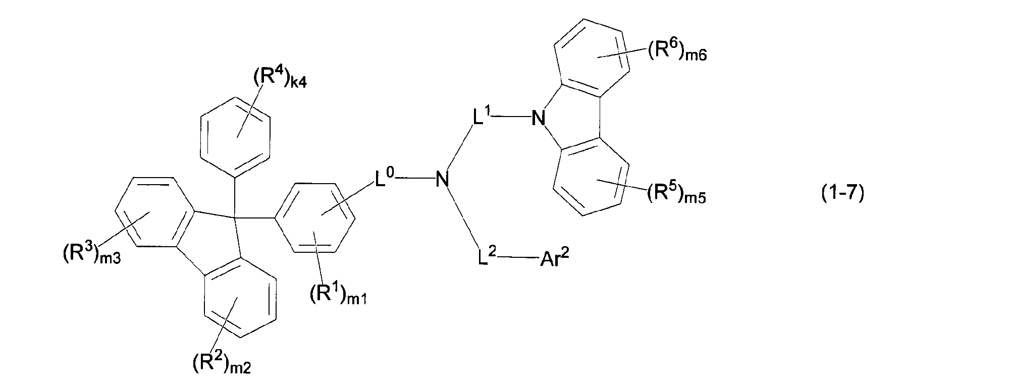
- 下記一般式(1-7-1)又は(1-7-2)で表される、請求項14に記載の化合物。
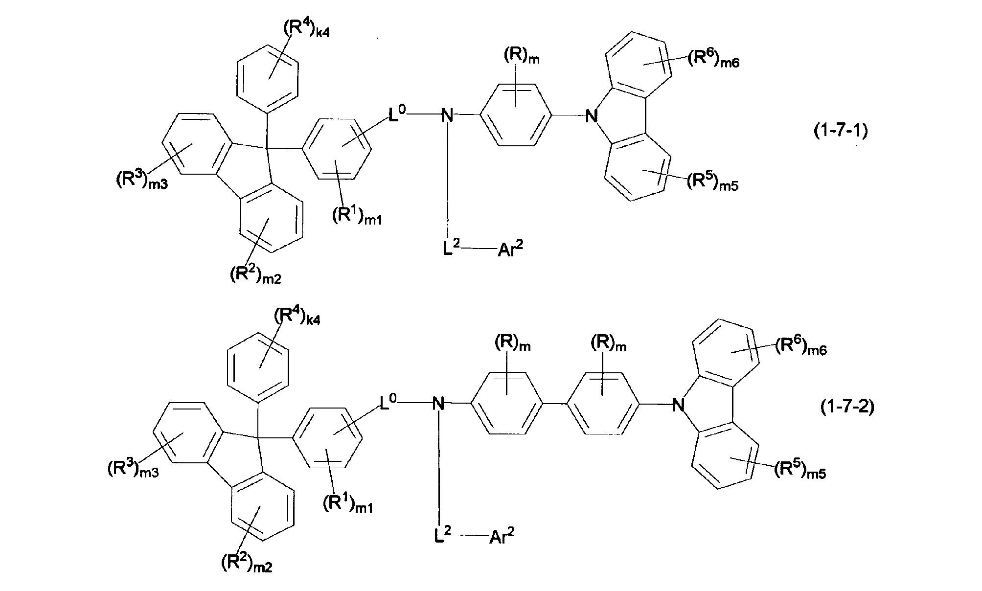
- Ar2が、下記一般式(a)~(h)のいずれかで表される基である、請求項14又は15に記載の化合物。
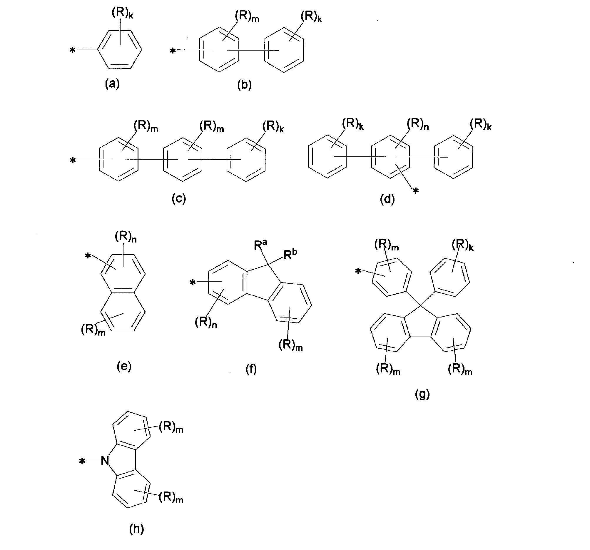
kは、それぞれ独立に、0~5の整数であり、mは、それぞれ独立に、0~4の整数であり、nは、それぞれ独立に、0~3の整数である。
*は、前記一般式(1)中のL2又は窒素原子との結合位置を示す。〕 - 請求項1~16のいずれか1項に記載の化合物からなる、有機エレクトロルミネッセンス素子用材料。
- 陰極、陽極、及び該陰極と該陽極の間に配置された一層以上の有機薄膜層を有し、該一層以上の有機薄膜層が発光層を含む有機エレクトロルミネッセンス素子であって、
前記一層以上の有機薄膜層の少なくとも1層が、請求項1~16のいずれか1項に記載の化合物を含む層である、有機エレクトロルミネッセンス素子。 - 前記一層以上の有機薄膜層が、前記化合物を含む正孔注入層及び前記化合物を含む正孔輸送層の少なくとも一方を含む、請求項18に記載の有機エレクトロルミネッセンス素子。
- 請求項18又は19に記載の有機エレクトロルミネッセンス素子を搭載した、電子機器。
Priority Applications (5)
| Application Number | Priority Date | Filing Date | Title |
|---|---|---|---|
| JP2015560882A JP6696091B2 (ja) | 2014-07-11 | 2015-07-13 | 化合物、有機エレクトロルミネッセンス素子用材料、有機エレクトロルミネッセンス素子、及び電子機器 |
| EP15819775.6A EP3029023A4 (en) | 2014-07-11 | 2015-07-13 | Compound, material for organic electroluminescent element, organic electroluminescent element, and electronic device |
| KR1020167002763A KR102572370B1 (ko) | 2014-07-11 | 2015-07-13 | 화합물, 유기 전기발광 소자용 재료, 유기 전기발광 소자, 및 전자 기기 |
| CN201580001553.1A CN105658620B (zh) | 2014-07-11 | 2015-07-13 | 化合物、有机电致发光元件用材料、有机电致发光元件和电子设备 |
| US14/910,596 US10756275B2 (en) | 2014-07-11 | 2015-07-13 | Compound, material for organic electroluminescence devices, organic electroluminescence device, and electronic equipment |
Applications Claiming Priority (2)
| Application Number | Priority Date | Filing Date | Title |
|---|---|---|---|
| JP2014143244 | 2014-07-11 | ||
| JP2014-143244 | 2014-07-11 |
Publications (1)
| Publication Number | Publication Date |
|---|---|
| WO2016006708A1 true WO2016006708A1 (ja) | 2016-01-14 |
Family
ID=55064332
Family Applications (1)
| Application Number | Title | Priority Date | Filing Date |
|---|---|---|---|
| PCT/JP2015/070044 Ceased WO2016006708A1 (ja) | 2014-07-11 | 2015-07-13 | 化合物、有機エレクトロルミネッセンス素子用材料、有機エレクトロルミネッセンス素子、及び電子機器 |
Country Status (6)
| Country | Link |
|---|---|
| US (1) | US10756275B2 (ja) |
| EP (1) | EP3029023A4 (ja) |
| JP (1) | JP6696091B2 (ja) |
| KR (1) | KR102572370B1 (ja) |
| CN (1) | CN105658620B (ja) |
| WO (1) | WO2016006708A1 (ja) |
Cited By (5)
| Publication number | Priority date | Publication date | Assignee | Title |
|---|---|---|---|---|
| JP2016113396A (ja) * | 2014-12-15 | 2016-06-23 | 三星ディスプレイ株式會社Samsung Display Co.,Ltd. | アミン化合物、および有機電界発光素子 |
| KR20170088650A (ko) * | 2016-01-25 | 2017-08-02 | 주식회사 엘지화학 | 화합물 및 이를 포함하는 유기 전자 소자 |
| WO2018164201A1 (ja) * | 2017-03-08 | 2018-09-13 | 出光興産株式会社 | 化合物、有機エレクトロルミネッセンス素子用材料、有機エレクトロルミネッセンス素子、及び電子機器 |
| US11608327B2 (en) | 2016-03-03 | 2023-03-21 | Merck Patent Gmbh | Materials for organic electroluminescent devices |
| KR20250007515A (ko) | 2022-04-26 | 2025-01-14 | 이데미쓰 고산 가부시키가이샤 | 화합물, 유기 전기발광 소자용 재료, 유기 전기발광 소자, 및 전자 기기 |
Families Citing this family (13)
| Publication number | Priority date | Publication date | Assignee | Title |
|---|---|---|---|---|
| KR102595922B1 (ko) * | 2015-12-22 | 2023-10-31 | 삼성디스플레이 주식회사 | 카바졸계 화합물 및 이를 포함한 유기 발광 소자 |
| CN108033886A (zh) * | 2017-12-01 | 2018-05-15 | 吉林奥来德光电材料股份有限公司 | 一种芴化合物及其制备方法和有机电致发光器件 |
| KR101857632B1 (ko) | 2018-02-02 | 2018-05-14 | 덕산네오룩스 주식회사 | 유기전기소자용 화합물, 이를 이용한 유기전기소자 및 그 전자 장치 |
| CN109748802A (zh) * | 2018-12-29 | 2019-05-14 | 吉林奥来德光电材料股份有限公司 | 一种有机电致发光化合物及制法和有机电致发光器件 |
| KR20210031332A (ko) | 2019-09-11 | 2021-03-19 | 삼성에스디아이 주식회사 | 유기 광전자 소자용 화합물, 유기 광전자 소자 및 표시 장치 |
| KR102893931B1 (ko) | 2019-11-25 | 2025-12-03 | 삼성디스플레이 주식회사 | 유기 발광 소자 |
| US20210226086A1 (en) * | 2020-01-21 | 2021-07-22 | Samsung Display Co., Ltd. | Light emitting element and display device including the same |
| EP3855524A1 (en) * | 2020-01-21 | 2021-07-28 | Samsung Display Co., Ltd. | Light emitting diode and display device including the same |
| KR102817317B1 (ko) * | 2020-07-22 | 2025-06-10 | 삼성디스플레이 주식회사 | 유기 발광 소자 |
| KR102870803B1 (ko) | 2020-08-20 | 2025-10-14 | 삼성디스플레이 주식회사 | 아민 화합물 및 이를 포함한 발광 소자 |
| KR102956632B1 (ko) * | 2020-12-07 | 2026-04-23 | 삼성디스플레이 주식회사 | 발광 소자 및 이를 포함하는 전자 장치 |
| CN114685289A (zh) * | 2022-04-20 | 2022-07-01 | 吉林奥来德光电材料股份有限公司 | 有机电致发光化合物及其制备方法和有机电致发光器件 |
| KR102739010B1 (ko) * | 2022-07-25 | 2024-12-06 | 덕산네오룩스 주식회사 | 유기전기 소자용 화합물, 이를 이용한 유기전기소자 및 그 전자 장치 |
Citations (8)
| Publication number | Priority date | Publication date | Assignee | Title |
|---|---|---|---|---|
| JP2003261472A (ja) * | 2002-03-07 | 2003-09-16 | Mitsui Chemicals Inc | 有機電界発光素子および新規炭化水素化合物 |
| JP2005085599A (ja) * | 2003-09-09 | 2005-03-31 | Toyo Ink Mfg Co Ltd | 有機エレクトロルミネッセンス素子 |
| JP2005120030A (ja) * | 2003-10-17 | 2005-05-12 | Mitsui Chemicals Inc | 9,9−ジフェニルフルオレン化合物、および該9,9−ジフェニルフルオレン化合物を含有する有機電界発光素子 |
| JP2009149850A (ja) * | 2007-11-30 | 2009-07-09 | Sumitomo Chemical Co Ltd | アミン系高分子化合物及びそれを用いた発光素子 |
| JP2011006405A (ja) * | 2009-05-29 | 2011-01-13 | Semiconductor Energy Lab Co Ltd | フルオレン誘導体、発光素子、発光装置、電子機器、及び照明装置 |
| WO2011021520A1 (ja) * | 2009-08-19 | 2011-02-24 | 出光興産株式会社 | 芳香族アミン誘導体及びそれを用いた有機エレクトロルミネッセンス素子 |
| US20140191214A1 (en) * | 2013-01-04 | 2014-07-10 | Samsung Display Co., Ltd. | Fluorene-based compound and organic light-emitting device including the same |
| CN104086447A (zh) * | 2014-06-25 | 2014-10-08 | 上海道亦化工科技有限公司 | 一种基于芴的空穴传输化合物 |
Family Cites Families (17)
| Publication number | Priority date | Publication date | Assignee | Title |
|---|---|---|---|---|
| JP3838766B2 (ja) | 1997-11-06 | 2006-10-25 | 三井化学株式会社 | 有機電界発光素子 |
| JP5268247B2 (ja) | 2005-12-20 | 2013-08-21 | キヤノン株式会社 | 4−アミノフルオレン化合物及び有機発光素子 |
| KR101453109B1 (ko) | 2006-04-26 | 2014-10-27 | 이데미쓰 고산 가부시키가이샤 | 방향족 아민 유도체 및 그들을 이용한 유기 전기 발광 소자 |
| KR101002733B1 (ko) * | 2007-09-14 | 2010-12-21 | 제일모직주식회사 | 유기 화합물, 및 이를 포함하는 유기광전소자 |
| KR101597994B1 (ko) * | 2007-12-03 | 2016-02-26 | 가부시키가이샤 한도오따이 에네루기 켄큐쇼 | 카바졸 유도체, 및 카바졸 유도체를 사용하는 발광 소자, 발광 장치 및 전자기기 |
| KR101211091B1 (ko) * | 2009-09-16 | 2012-12-12 | 주식회사 진웅산업 | 유기 발광 화합물 및 이를 이용한 유기 전계발광 소자 |
| KR101311935B1 (ko) | 2010-04-23 | 2013-09-26 | 제일모직주식회사 | 유기광전소자용 화합물 및 이를 포함하는 유기광전소자 |
| JP2012224618A (ja) | 2011-04-08 | 2012-11-15 | Fujifilm Corp | 有機材料の精製方法、有機エレクトロニクス用材料、光電変換素子、光センサ、撮像素子、及び有機電界発光素子 |
| KR20180126629A (ko) | 2011-12-12 | 2018-11-27 | 메르크 파텐트 게엠베하 | 전자 소자용 화합물 |
| CN104603111A (zh) | 2012-07-23 | 2015-05-06 | 默克专利有限公司 | 芴和含有所述芴的电子器件 |
| CN107445930A (zh) | 2012-08-31 | 2017-12-08 | 出光兴产株式会社 | 芳香族胺衍生物和使用了其的有机电致发光元件 |
| KR101684979B1 (ko) * | 2012-12-31 | 2016-12-09 | 제일모직 주식회사 | 유기광전자소자 및 이를 포함하는 표시장치 |
| KR101389527B1 (ko) | 2013-09-17 | 2014-04-25 | 덕산하이메탈(주) | 유기전기 소자용 화합물을 이용한 유기전기소자 및 그 전자 장치 |
| CN103755574A (zh) | 2014-01-26 | 2014-04-30 | 黑龙江省科学院石油化学研究院 | 一种具有多光子吸收性质的三(9,9-二烷基-9h-芴基)胺的合成方法 |
| KR101931250B1 (ko) * | 2014-05-13 | 2018-12-20 | 제일모직 주식회사 | 화합물, 이를 포함하는 유기 광전자 소자 및 표시장치 |
| WO2015174640A1 (ko) * | 2014-05-13 | 2015-11-19 | 삼성에스디아이 주식회사 | 화합물, 이를 포함하는 유기 광전자 소자 및 표시장치 |
| JP2016041634A (ja) * | 2014-08-15 | 2016-03-31 | 日本板硝子株式会社 | 合わせガラス |
-
2015
- 2015-07-13 US US14/910,596 patent/US10756275B2/en active Active
- 2015-07-13 JP JP2015560882A patent/JP6696091B2/ja active Active
- 2015-07-13 KR KR1020167002763A patent/KR102572370B1/ko active Active
- 2015-07-13 CN CN201580001553.1A patent/CN105658620B/zh active Active
- 2015-07-13 WO PCT/JP2015/070044 patent/WO2016006708A1/ja not_active Ceased
- 2015-07-13 EP EP15819775.6A patent/EP3029023A4/en active Pending
Patent Citations (8)
| Publication number | Priority date | Publication date | Assignee | Title |
|---|---|---|---|---|
| JP2003261472A (ja) * | 2002-03-07 | 2003-09-16 | Mitsui Chemicals Inc | 有機電界発光素子および新規炭化水素化合物 |
| JP2005085599A (ja) * | 2003-09-09 | 2005-03-31 | Toyo Ink Mfg Co Ltd | 有機エレクトロルミネッセンス素子 |
| JP2005120030A (ja) * | 2003-10-17 | 2005-05-12 | Mitsui Chemicals Inc | 9,9−ジフェニルフルオレン化合物、および該9,9−ジフェニルフルオレン化合物を含有する有機電界発光素子 |
| JP2009149850A (ja) * | 2007-11-30 | 2009-07-09 | Sumitomo Chemical Co Ltd | アミン系高分子化合物及びそれを用いた発光素子 |
| JP2011006405A (ja) * | 2009-05-29 | 2011-01-13 | Semiconductor Energy Lab Co Ltd | フルオレン誘導体、発光素子、発光装置、電子機器、及び照明装置 |
| WO2011021520A1 (ja) * | 2009-08-19 | 2011-02-24 | 出光興産株式会社 | 芳香族アミン誘導体及びそれを用いた有機エレクトロルミネッセンス素子 |
| US20140191214A1 (en) * | 2013-01-04 | 2014-07-10 | Samsung Display Co., Ltd. | Fluorene-based compound and organic light-emitting device including the same |
| CN104086447A (zh) * | 2014-06-25 | 2014-10-08 | 上海道亦化工科技有限公司 | 一种基于芴的空穴传输化合物 |
Cited By (10)
| Publication number | Priority date | Publication date | Assignee | Title |
|---|---|---|---|---|
| JP2016113396A (ja) * | 2014-12-15 | 2016-06-23 | 三星ディスプレイ株式會社Samsung Display Co.,Ltd. | アミン化合物、および有機電界発光素子 |
| KR20170088650A (ko) * | 2016-01-25 | 2017-08-02 | 주식회사 엘지화학 | 화합물 및 이를 포함하는 유기 전자 소자 |
| KR101896151B1 (ko) * | 2016-01-25 | 2018-09-07 | 주식회사 엘지화학 | 화합물 및 이를 포함하는 유기 전자 소자 |
| US11608327B2 (en) | 2016-03-03 | 2023-03-21 | Merck Patent Gmbh | Materials for organic electroluminescent devices |
| US12065431B2 (en) | 2016-03-03 | 2024-08-20 | Merck Patent Gmbh | Materials for organic electroluminescent devices |
| US12441715B2 (en) | 2016-03-03 | 2025-10-14 | Merck Patent Gmbh | Materials for organic electroluminescent devices |
| US12583842B2 (en) | 2016-03-03 | 2026-03-24 | Merck Patent Gmbh | Materials for organic electroluminescent devices |
| WO2018164201A1 (ja) * | 2017-03-08 | 2018-09-13 | 出光興産株式会社 | 化合物、有機エレクトロルミネッセンス素子用材料、有機エレクトロルミネッセンス素子、及び電子機器 |
| US11053229B2 (en) | 2017-03-08 | 2021-07-06 | Idemitsu Kosan Co., Ltd. | Compound, material for organic electroluminescent element, organic electroluminescent element, and electronic device |
| KR20250007515A (ko) | 2022-04-26 | 2025-01-14 | 이데미쓰 고산 가부시키가이샤 | 화합물, 유기 전기발광 소자용 재료, 유기 전기발광 소자, 및 전자 기기 |
Also Published As
| Publication number | Publication date |
|---|---|
| US10756275B2 (en) | 2020-08-25 |
| KR102572370B1 (ko) | 2023-08-29 |
| US20160197277A1 (en) | 2016-07-07 |
| EP3029023A4 (en) | 2017-01-18 |
| JP6696091B2 (ja) | 2020-05-20 |
| CN105658620B (zh) | 2020-12-29 |
| KR20170030450A (ko) | 2017-03-17 |
| JPWO2016006708A1 (ja) | 2017-04-27 |
| CN105658620A (zh) | 2016-06-08 |
| EP3029023A1 (en) | 2016-06-08 |
Similar Documents
| Publication | Publication Date | Title |
|---|---|---|
| JP6601627B2 (ja) | 化合物、有機エレクトロルミネッセンス素子用材料、有機エレクトロルミネッセンス素子、及び電子機器 | |
| JP6696091B2 (ja) | 化合物、有機エレクトロルミネッセンス素子用材料、有機エレクトロルミネッセンス素子、及び電子機器 | |
| JP7461300B2 (ja) | 化合物、有機エレクトロルミネッセンス素子用材料、有機エレクトロルミネッセンス素子、及び、電子機器 | |
| JP6454226B2 (ja) | 化合物、有機エレクトロルミネッセンス素子用材料、有機エレクトロルミネッセンス素子、及び電子機器 | |
| JP7253502B2 (ja) | 化合物及びそれを用いた有機エレクトロルミネッセンス素子 | |
| JP6419874B2 (ja) | 化合物、有機エレクトロルミネッセンス素子用材料、有機エレクトロルミネッセンス素子及び電子機器 | |
| JPWO2017022730A1 (ja) | 化合物、有機エレクトロルミネッセンス素子用材料、有機エレクトロルミネッセンス素子、及び電子機器 | |
| WO2016204150A1 (ja) | 化合物、有機エレクトロルミネッセンス素子用材料、有機エレクトロルミネッセンス素子及び電子機器 | |
| WO2016056640A1 (ja) | 化合物、有機エレクトロルミネッセンス素子用材料、有機エレクトロルミネッセンス素子、及び電子機器 | |
| WO2016133097A1 (ja) | 化合物、有機エレクトロルミネッセンス素子用材料、有機エレクトロルミネッセンス素子、及び電子機器 |
Legal Events
| Date | Code | Title | Description |
|---|---|---|---|
| ENP | Entry into the national phase |
Ref document number: 2015560882 Country of ref document: JP Kind code of ref document: A |
|
| ENP | Entry into the national phase |
Ref document number: 20167002763 Country of ref document: KR Kind code of ref document: A |
|
| WWE | Wipo information: entry into national phase |
Ref document number: 14910596 Country of ref document: US Ref document number: 2015819775 Country of ref document: EP |
|
| 121 | Ep: the epo has been informed by wipo that ep was designated in this application |
Ref document number: 15819775 Country of ref document: EP Kind code of ref document: A1 |
|
| NENP | Non-entry into the national phase |
Ref country code: DE |