WO2016009714A1 - 半導体装置 - Google Patents
半導体装置 Download PDFInfo
- Publication number
- WO2016009714A1 WO2016009714A1 PCT/JP2015/064221 JP2015064221W WO2016009714A1 WO 2016009714 A1 WO2016009714 A1 WO 2016009714A1 JP 2015064221 W JP2015064221 W JP 2015064221W WO 2016009714 A1 WO2016009714 A1 WO 2016009714A1
- Authority
- WO
- WIPO (PCT)
- Prior art keywords
- region
- trench
- diode
- igbt
- boundary
- Prior art date
- Legal status (The legal status is an assumption and is not a legal conclusion. Google has not performed a legal analysis and makes no representation as to the accuracy of the status listed.)
- Ceased
Links
Images


Classifications
-
- H—ELECTRICITY
- H10—SEMICONDUCTOR DEVICES; ELECTRIC SOLID-STATE DEVICES NOT OTHERWISE PROVIDED FOR
- H10D—INORGANIC ELECTRIC SEMICONDUCTOR DEVICES
- H10D84/00—Integrated devices formed in or on semiconductor substrates that comprise only semiconducting layers, e.g. on Si wafers or on GaAs-on-Si wafers
- H10D84/60—Integrated devices formed in or on semiconductor substrates that comprise only semiconducting layers, e.g. on Si wafers or on GaAs-on-Si wafers characterised by the integration of at least one component covered by groups H10D10/00 or H10D18/00, e.g. integration of BJTs
- H10D84/611—Combinations of BJTs and one or more of diodes, resistors or capacitors
- H10D84/613—Combinations of vertical BJTs and one or more of diodes, resistors or capacitors
- H10D84/617—Combinations of vertical BJTs and only diodes
-
- H—ELECTRICITY
- H10—SEMICONDUCTOR DEVICES; ELECTRIC SOLID-STATE DEVICES NOT OTHERWISE PROVIDED FOR
- H10D—INORGANIC ELECTRIC SEMICONDUCTOR DEVICES
- H10D84/00—Integrated devices formed in or on semiconductor substrates that comprise only semiconducting layers, e.g. on Si wafers or on GaAs-on-Si wafers
- H10D84/80—Integrated devices formed in or on semiconductor substrates that comprise only semiconducting layers, e.g. on Si wafers or on GaAs-on-Si wafers characterised by the integration of at least one component covered by groups H10D12/00 or H10D30/00, e.g. integration of IGFETs
- H10D84/811—Combinations of field-effect devices and one or more diodes, capacitors or resistors
-
- H—ELECTRICITY
- H10—SEMICONDUCTOR DEVICES; ELECTRIC SOLID-STATE DEVICES NOT OTHERWISE PROVIDED FOR
- H10D—INORGANIC ELECTRIC SEMICONDUCTOR DEVICES
- H10D12/00—Bipolar devices controlled by the field effect, e.g. insulated-gate bipolar transistors [IGBT]
- H10D12/411—Insulated-gate bipolar transistors [IGBT]
- H10D12/441—Vertical IGBTs
- H10D12/461—Vertical IGBTs having non-planar surfaces, e.g. having trenches, recesses or pillars in the surfaces of the emitter, base or collector regions
- H10D12/481—Vertical IGBTs having non-planar surfaces, e.g. having trenches, recesses or pillars in the surfaces of the emitter, base or collector regions having gate structures on slanted surfaces, on vertical surfaces, or in grooves, e.g. trench gate IGBTs
-
- H—ELECTRICITY
- H10—SEMICONDUCTOR DEVICES; ELECTRIC SOLID-STATE DEVICES NOT OTHERWISE PROVIDED FOR
- H10D—INORGANIC ELECTRIC SEMICONDUCTOR DEVICES
- H10D30/00—Field-effect transistors [FET]
- H10D30/60—Insulated-gate field-effect transistors [IGFET]
-
- H—ELECTRICITY
- H10—SEMICONDUCTOR DEVICES; ELECTRIC SOLID-STATE DEVICES NOT OTHERWISE PROVIDED FOR
- H10D—INORGANIC ELECTRIC SEMICONDUCTOR DEVICES
- H10D62/00—Semiconductor bodies, or regions thereof, of devices having potential barriers
- H10D62/10—Shapes, relative sizes or dispositions of the regions of the semiconductor bodies; Shapes of the semiconductor bodies
- H10D62/124—Shapes, relative sizes or dispositions of the regions of semiconductor bodies or of junctions between the regions
- H10D62/126—Top-view geometrical layouts of the regions or the junctions
- H10D62/127—Top-view geometrical layouts of the regions or the junctions of cellular field-effect devices, e.g. multicellular DMOS transistors or IGBTs
-
- H—ELECTRICITY
- H10—SEMICONDUCTOR DEVICES; ELECTRIC SOLID-STATE DEVICES NOT OTHERWISE PROVIDED FOR
- H10D—INORGANIC ELECTRIC SEMICONDUCTOR DEVICES
- H10D62/00—Semiconductor bodies, or regions thereof, of devices having potential barriers
- H10D62/10—Shapes, relative sizes or dispositions of the regions of the semiconductor bodies; Shapes of the semiconductor bodies
- H10D62/128—Anode regions of diodes
-
- H—ELECTRICITY
- H10—SEMICONDUCTOR DEVICES; ELECTRIC SOLID-STATE DEVICES NOT OTHERWISE PROVIDED FOR
- H10D—INORGANIC ELECTRIC SEMICONDUCTOR DEVICES
- H10D62/00—Semiconductor bodies, or regions thereof, of devices having potential barriers
- H10D62/10—Shapes, relative sizes or dispositions of the regions of the semiconductor bodies; Shapes of the semiconductor bodies
- H10D62/13—Semiconductor regions connected to electrodes carrying current to be rectified, amplified or switched, e.g. source or drain regions
- H10D62/141—Anode or cathode regions of thyristors; Collector or emitter regions of gated bipolar-mode devices, e.g. of IGBTs
- H10D62/142—Anode regions of thyristors or collector regions of gated bipolar-mode devices
-
- H—ELECTRICITY
- H10—SEMICONDUCTOR DEVICES; ELECTRIC SOLID-STATE DEVICES NOT OTHERWISE PROVIDED FOR
- H10D—INORGANIC ELECTRIC SEMICONDUCTOR DEVICES
- H10D62/00—Semiconductor bodies, or regions thereof, of devices having potential barriers
- H10D62/10—Shapes, relative sizes or dispositions of the regions of the semiconductor bodies; Shapes of the semiconductor bodies
- H10D62/17—Semiconductor regions connected to electrodes not carrying current to be rectified, amplified or switched, e.g. channel regions
- H10D62/393—Body regions of DMOS transistors or IGBTs
-
- H—ELECTRICITY
- H10—SEMICONDUCTOR DEVICES; ELECTRIC SOLID-STATE DEVICES NOT OTHERWISE PROVIDED FOR
- H10D—INORGANIC ELECTRIC SEMICONDUCTOR DEVICES
- H10D8/00—Diodes
-
- H—ELECTRICITY
- H10—SEMICONDUCTOR DEVICES; ELECTRIC SOLID-STATE DEVICES NOT OTHERWISE PROVIDED FOR
- H10D—INORGANIC ELECTRIC SEMICONDUCTOR DEVICES
- H10D64/00—Electrodes of devices having potential barriers
- H10D64/111—Field plates
- H10D64/117—Recessed field plates, e.g. trench field plates or buried field plates
-
- H—ELECTRICITY
- H10—SEMICONDUCTOR DEVICES; ELECTRIC SOLID-STATE DEVICES NOT OTHERWISE PROVIDED FOR
- H10D—INORGANIC ELECTRIC SEMICONDUCTOR DEVICES
- H10D8/00—Diodes
- H10D8/422—PN diodes having the PN junctions in mesas
Definitions
- the technology disclosed in this specification relates to a semiconductor device.
- Patent Document 1 discloses a semiconductor device (so-called RC-IGBT) in which a diode and an IGBT are formed on the same semiconductor substrate.
- Patent Document 1 discloses a technique in which a contact portion (a portion that conducts to an electrode) of an IGBT body region is made smaller than a contact portion of an anode region of a diode in order to suppress gate interference. According to this configuration, since the holes flowing from the body region of the IGBT into the drift region of the diode are reduced, the influence of gate interference can be reduced. However, in this configuration, since the contact portion of the anode region is large, high-concentration holes flow from the anode region into the drift region during diode operation, and the concentration of holes in the drift region increases. For this reason, the reverse recovery characteristic of the diode deteriorates.
- the present specification provides a semiconductor device in which the response speed of a diode is high and the influence of gate interference is small.
- a semiconductor device disclosed in this specification includes a semiconductor substrate, a surface electrode formed on the surface of the semiconductor substrate, and a back electrode formed on the back surface of the semiconductor substrate.
- the semiconductor substrate includes a first IGBT region located between the first trench and the first boundary trench, a diode region located between the first boundary trench and the second boundary trench, and the second trench.
- a second IGBT region is provided between the second boundary trenches.
- a gate insulating film and a gate electrode insulated from the semiconductor substrate by the gate insulating film are disposed in each of the first trench and the second trench.
- An interlayer insulating film is disposed between each gate electrode and the surface electrode.
- An insulating layer is disposed inside each of the first boundary trench and the second boundary trench.
- Each of the body regions has a body contact portion that has a p-type impurity concentration of 1 ⁇ 10 18 atoms / cm 3 or more on the surface and is in contact with the surface electrode.
- a p-type anode region in contact with the surface electrode is formed in the diode region.
- the anode region has an anode contact portion having a p-type impurity concentration on the surface of 1 ⁇ 10 18 atoms / cm 3 or more and in contact with the surface electrode.
- An n-type region extending across the first IGBT region, the second IGBT region, and the diode region is formed in a region on the back side of each body region and the anode region.
- the n-type region is in contact with the back electrode at least at a part of the diode region.
- a p-type in contact with at least a part of a region on the back side of the n-type region in the first IGBT region and at least a part of a region on the back side of the n-type region in the second IGBT region.
- the collector region is formed.
- An interval between the first boundary trench and the second boundary trench is 200 ⁇ m or more.
- the ratio of the area of the anode contact portion to the surface in the diode region occupies the ratio of the area of the body contact portion to the surface in the first IGBT region and the surface in the second IGBT region. It is lower than any of the ratio of the area of the body contact portion.
- the ratio of the area of the predetermined portion occupying the predetermined surface means a value obtained by dividing the area of the predetermined portion by the area of the predetermined surface.
- the ratio of the area of the anode contact portion to the surface in the diode region means a value obtained by dividing the area of the anode contact portion by the area of the surface in the diode region.
- the “interval between the first boundary trench and the second boundary trench” is the center line of the first boundary trench and the center of the second boundary trench when the surface of the semiconductor substrate is viewed in plan. It means the distance between lines.
- the amount of holes flowing from the anode region to the drift region when the diode is energized can be reduced. Become more. Further, holes flowing from the body region to the drift region when the diode is energized flow only in the vicinity of the boundary between the IGBT region and the diode region, and therefore do not increase even if the width of the diode region is increased. Therefore, by increasing the width of the diode region, the ratio of holes flowing through the body region to holes flowing through the anode region can be reduced.
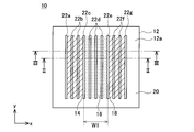
- FIG. 2 is a plan view of the semiconductor device 10.
- FIG. 2 is a longitudinal sectional view taken along line II-II in FIG.
- FIG. 3 is a longitudinal sectional view taken along line III-III in FIG. 1.
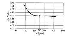
- FIG. 4 is an enlarged plan view of a semiconductor substrate 10 in the vicinity of a trench 22c. The graph which shows the relationship between Vfp-Vfa and the space
- FIG. 6 is an enlarged plan view of a semiconductor substrate 10 in the vicinity of a trench 22c of a semiconductor device of Example 2.
- a plurality of third trenches extending along the first boundary trench may be formed on the surface in the diode region.
- the anode region including the anode contact portion is formed in each of the diode cell regions sandwiched between any two of the plurality of third trenches, the first boundary trench, and the second boundary trench in the diode region. May be.
- a plurality of fourth trenches extending along the first boundary trench may be formed in each of the first IGBT region and the second IGBT region.
- a gate insulating film and a gate electrode may be formed in each of the fourth trenches.
- An emitter region and a body region including a body contact portion may be formed in each of the IGBT cell regions sandwiched between any two of the plurality of fourth trenches, the first boundary trenches, and the second boundary trenches.
- Good. (Characteristic 3) In each diode cell region, the ratio of the area of the anode contact portion to the surface in the diode cell region is lower than any of the ratio of the area of the body contact portion to the surface in the IGBT cell region.
- Each anode contact portion may extend along the third trench.
- Each diode cell region may have a plurality of anode contact portions separated from each other.
- a plurality of anode contact portions may be arranged along the third trench in each diode cell region. (Feature 6) Each anode contact portion in the diode cell region adjacent to the first boundary trench is disposed at a position in the width direction of the first boundary trench as viewed from the emitter region in the IGBT cell region adjacent to the first boundary trench. Has been.
- FIG. 1 includes a semiconductor substrate 12 made of silicon.
- FIG. 1 illustration of electrodes, insulating layers and the like formed on the surface (front surface) 12a of the semiconductor substrate 12 is omitted.
- a plurality of trenches 22 are formed on the surface 12 a of the semiconductor substrate 12.
- the plurality of trenches 22 extend in parallel to each other in plan view of the surface 12a.
- the longitudinal direction of the trench 22 in FIG. 1 is referred to as the y direction
- the direction orthogonal to the y direction in FIG. 1 is referred to as the x direction.
- the semiconductor substrate 12 can be partitioned into a first IGBT region 14, a diode region 16, a second IGBT region 18, and an outer peripheral region 20 in a plan view of the surface 12 a.
- first IGBT region 14 and the second IGBT region 18 are indicated by hatching
- the diode region 16 is indicated by dot hatching.
- IGBTs are formed in the first IGBT region 14 and the second IGBT region 18, and diodes are formed in the diode region 16.
- the first IGBT region 14 is formed between the trench 22a and the trench 22c among the plurality of trenches 22. More specifically, the first IGBT region 14 is a region surrounded by a trench 22a, a trench 22c, and a straight line connecting both ends of the trench 22a and the trench 22c in a plan view of the surface 12a. On the surface 12 a in the first IGBT region 14, some of the plurality of trenches 22 (a plurality of trenches 22 b) are formed.
- the second IGBT region 18 is formed between the trench 22e and the trench 22g among the plurality of trenches 22. More specifically, the second IGBT region 18 is a region surrounded by a trench 22e, a trench 22g, and a straight line connecting both ends of the trench 22e and the trench 22g in a plan view of the surface 12a. On the surface 12 a in the second IGBT region 18, some of the plurality of trenches 22 (a plurality of trenches 22 f) are formed.
- the diode region 16 is formed between the trench 22c and the trench 22e among the plurality of trenches 22. More specifically, the diode region 16 is a region surrounded by a trench 22c, a trench 22e, and a straight line connecting both ends of the trench 22c and the trench 22e in a plan view of the surface 12a. The diode region 16 is disposed between the first IGBT region 14 and the second IGBT region 18. A part of the plurality of trenches 22 (a plurality of trenches 22 d) is formed on the surface 12 a in the diode region 16.
- the outer peripheral region 20 is a region near the outer peripheral end of the semiconductor substrate 12.
- the outer peripheral region 20 is formed around the first IGBT region 14, the diode region 16, and the second IGBT region 18.
- each trench 22 (that is, trenches 22 a to 22 g) extends from the surface 12 a of the semiconductor substrate 12 in the thickness direction of the semiconductor substrate 12.
- An insulating film 24 is formed inside each trench 22.
- the insulating film 24 covers the bottom and side surfaces of each trench 22.
- a gate electrode 26 is disposed in the trenches 22a, 22b, 22c, 22e, 22f and 22g.
- the gate electrode 26 is insulated from the semiconductor substrate 12 by the insulating film 24.
- a control electrode 28 is disposed in the trench 22d.
- the control electrode 28 is insulated from the semiconductor substrate 12 by the insulating film 24.
- Each gate electrode 26 is connected to a gate pad by a wiring (not shown).
- the potential of the gate electrode 26 can be controlled independently of the potential of the control electrode 28.
- the control electrode 28 is connected to the emitter electrode 32.
- the upper surface of the gate electrode 26 is covered with an interlayer insulating film 30.
- the semiconductor region sandwiched between the two trenches 22 among the semiconductor regions in the first IGBT region 14 and the second IGBT region 18 is referred to as a cell region 40.
- a semiconductor region sandwiched between the two trenches 22 among the semiconductor regions in the diode region 16 is referred to as a cell region 42.
- a surface electrode 32 made of aluminum is formed on the surface 12a of the semiconductor substrate 12.
- the surface electrode 32 is insulated from each gate electrode 26 and each control electrode 28 by the interlayer insulating film 30.
- An aluminum back electrode 34 is formed on the back surface 12 b of the semiconductor substrate 12.
- FIG. 4 shows the surface 12a of the cell regions 40 and 42 in the vicinity of the trench 22c.
- the trench 22 is indicated by hatching for the sake of easy viewing.
- the cell region 40 adjacent to the trench 22c is referred to as a cell region 40a
- the cell region 42 adjacent to the trench 22c is referred to as a cell region 42a.
- a p-type anode region 50 is formed in the cell region 42a.
- the anode region 50 is exposed on the surface 12 a of the semiconductor substrate 12.
- the anode region 50 extends from the surface 12a to a position shallower than the lower end of the gate electrode 26 and the lower end of the control electrode 28 (position on the surface 12a side).
- the anode region 50 a heavily doped region 50a where the p-type impurity concentration is 1 ⁇ 10 18 atoms / cm 3 or more, p-type impurity concentration has a low density region 50b is less than 1 ⁇ 10 18 atoms / cm 3 ing.
- the high concentration region 50a is formed only in the vicinity of the surface 12a.
- the high concentration region 50a is formed at the center of the cell region 42a in the x direction.
- the high concentration region 50a is exposed on the surface 12a.
- the high concentration region 50a extends long in the y direction along the trench 22.
- the low concentration region 50b is exposed to the surface 12a on the side of the high concentration region 50a.
- the low concentration region 50b is also formed below the high concentration region 50a.
- the high concentration region 50a and the low concentration region 50b are in contact with the surface electrode 32 on the surface 12a. Since the p-type impurity concentration in the high concentration region 50a is high, the barrier existing between the high concentration region 50a and the surface electrode 32 is small. That is, the high concentration region 50 a is ohmically connected to the surface electrode 32.
- the contact surface between the high concentration region 50a and the surface electrode 32 is referred to as a contact portion 50c.
- the contact portion 50 c extends long in the y direction along the trench 22.
- the p-type impurity concentration of the low concentration region 50 b is low, a high barrier exists between the low concentration region 50 b and the surface electrode 32. That is, the low concentration region 50 b is Schottky connected to the surface electrode 32.
- Each cell region 42 has the same structure as the cell region 42a described above.
- an n-type region in contact with the surface electrode 32 and the insulating film 24 is not formed unlike an emitter region 52 described later.
- the region where the n-type region in contact with the surface electrode 32 and the insulating film 24 is not formed corresponds to the diode region 16.
- no n-type region is formed in the anode region 50, but an n-type region other than the n-type region in contact with the surface electrode 32 and the insulating film 24 is formed in the anode region 50. May be.
- an n-type region that contacts the insulating film 24 but does not contact the surface electrode 32 may be formed inside the anode region 50.
- an emitter region 52 and a body region 54 are formed in the cell region 40a.
- the emitter region 52 is n-type and is exposed on the surface 12 a of the semiconductor substrate 12.
- the emitter region 52 is formed only near the surface 12a.
- a plurality of emitter regions 52 are formed in the cell region 40a at intervals in the y direction.
- the emitter region 52 is in contact with the surface electrode 32 on the surface 12a. Since the n-type impurity concentration in the emitter region 52 is high, the barrier existing between the emitter region 52 and the surface electrode 32 is small. That is, the emitter region 52 is ohmically connected to the surface electrode 32.
- the emitter region 52 is in contact with the insulating film 24 in the trench 22 on both sides of the cell region 40a.
- the body region 54 is p-type and is exposed to the surface 12a at a position where the emitter region 52 is not formed.
- the body region 54 extends from the surface 12 a to a position shallower than the lower end of the gate electrode 26 and the lower end of the control electrode 28.
- the body region 54 is in contact with the insulating film 24 in the trench 22 on both sides of the cell region 40a.
- the body region 54 is also formed below the emitter region 52.
- the body region 54 is in contact with the insulating film 24 in the trench 22 on both sides of the cell region 40a below the emitter region 52.
- Body region 54 a heavily doped region 54a where the p-type impurity concentration is 1 ⁇ 10 18 atoms / cm 3 or more, p-type impurity concentration has a low density region 54b is less than 1 ⁇ 10 18 atoms / cm 3 ing.
- the high concentration region 54a is formed only in the vicinity of the surface 12a.
- the high concentration region 54a is exposed on the surface 12a.
- the low concentration region 54b is exposed to the surface 12a on the side of the high concentration region 54a.
- the body region 54 closer to the back surface 12b than the emitter region 52 and the high concentration region 54a is a low concentration region 54b.
- the p-type impurity concentration in the high concentration region 54a is high, the barrier existing between the high concentration region 54a and the surface electrode 32 is small. That is, the high concentration region 54 a is ohmically connected to the surface electrode 32.
- the contact surface between the high concentration region 54a and the surface electrode 32 is referred to as a contact portion 54c. Since the p-type impurity concentration of the low concentration region 54 b is low, a high barrier exists between the low concentration region 54 b and the surface electrode 32. That is, the low concentration region 54 b is Schottky connected to the surface electrode 32.
- the high concentration region 54a of the body region 54 and the high concentration region 50a of the anode region 50 are formed at a time by implanting p-type ions. For this reason, the p-type impurity concentration of the high concentration region 54a is substantially equal to the p-type impurity concentration of the high concentration region 50a.
- the depth of the high concentration region 54a is substantially equal to the depth of the high concentration region 50a.
- Each cell region 40 has the same structure as the cell region 40a described above.
- the emitter region 52 and the body region 54 have the same position in the y direction. Accordingly, when the surface 12a is viewed in plan, the emitter region 52 and the body region 54 appear to extend in the x direction across the trench 22.
- n-type drift region 56 is formed in a region on the back surface 12b side of the anode region 50 and the body region 54.
- the n-type impurity concentration in the drift region 56 is low.
- the drift region 56 extends between the first IGBT region 14, the diode region 16, and the second IGBT region 18. That is, the drift region 56 is continuous between the first IGBT region 14, the diode region 16, and the second IGBT region 18.
- Drift region 56 is separated from emitter region 52 by body region 54.
- the drift region 56 is in contact with the anode region 50 and the body region 54.
- the drift region 56 is in contact with the insulating film 24 near the lower end of each trench 22. Therefore, each gate electrode 26 and each control electrode 28 are opposed to the emitter region 52, the body region 54, and the drift region 56 through the insulating film 24.
- An n-type cathode region 60 is formed in a region on the back surface 12 b side of the drift region 56 in the diode region 16.
- the cathode region 60 has an n-type impurity concentration higher than that of the drift region 56.
- the cathode region 60 is in contact with the drift region 56.
- the cathode region 60 is exposed on the back surface 12b.
- the cathode region 60 is in contact with the back electrode 34 on the back surface 12b.
- the cathode region 60 is ohmically connected to the back electrode 34.
- a p-type collector region 58 is formed in the region on the back surface 12b side of the drift region 56 in the first IGBT region 14.
- the collector region 58 is in contact with the drift region 56.
- the collector region 58 is exposed on the back surface 12b.
- the collector region 58 is in contact with the back electrode 34 on the back surface 12b.
- the collector region 58 is ohmically connected to the back electrode 34.
- a p-type collector region 62 is formed in the region on the back surface 12 b side of the drift region 56 in the second IGBT region 18. Collector region 62 is in contact with drift region 56. The collector region 62 is exposed on the back surface 12b. The collector region 62 is in contact with the back electrode 34 on the back surface 12b. The collector region 62 is ohmically connected to the back electrode 34.
- a diode is formed by the anode region 50, the drift region 56 and the cathode region 60.
- an IGBT is formed by the emitter region 52, the body region 54, the drift region 56, the collector region 58, the gate electrode 26 and the insulating film 24.
- the interval W1 shown in FIGS. 1 to 3 indicates the interval between the trench 22c and the trench 22e. More specifically, the interval W1 indicates the interval between the center line of the trench 22c and the center line of the trench 22e when the surface 12a is viewed in plan.
- the interval W1 represents the width of the diode region 16.
- the interval W1 is 200 ⁇ m or more.
- the contact area ratio is a ratio of the contact portion in a predetermined region.
- the area of the surface 12a of each cell region 42 that is, the semiconductor region in the diode region 16 sandwiched between the two trenches 22
- the area of the contact portion 50c in each cell region 42 is S2
- each cell The area on the surface 12a of the region 40 that is, the semiconductor region in the IGBT regions 14 and 18 sandwiched between the two trenches 22
- S3 the area of the contact portion 54c in each cell region 40 is S4.
- the area of the surface 12a of the first IGBT region 14 is SI1
- the area of the surface 12a of the diode region 16 is Sd
- the area of the surface 12a of the second IGBT region 18 is SI2.
- the total area of the contact portion 54c in the first 1IGBT region 14 and Shigumaesu2 -1, the total area of the contact portion 54c in the first 2IGBT region 18 and Shigumaesu2 -2, the total area of the contact portion 50c in the diode region 16 Let ⁇ S4.
- the contact area ratio of the cell region 42 is S2 / S1, and the contact area ratio of the cell region 40 is S4 / S3.
- the contact area ratio S2 / S1 is slightly different for each cell region 42 due to an error or the like, the contact area ratios S2 / S1 of the cell regions 42 are substantially equal to each other.
- the contact area ratio S4 / S3 is slightly different for each cell region 40 due to an error or the like, the contact area ratios S4 / S3 of each cell region 40 are substantially equal to each other.
- S2 / S1 ⁇ S4 / S3 is satisfied. That is, the contact area ratio S2 / S1 of each cell region 42 is lower than any of the contact area ratios S4 / S3 of each cell region 40.
- the contact area ratio of the first IGBT region 14 is ⁇ S2 ⁇ 1 / SI1.
- the contact area ratio of the second IGBT region 18 is ⁇ S2 ⁇ 2 / SI2. Since S2 / S1 ⁇ S4 / S3 is satisfied, in the semiconductor device 10, S2 / S1 ⁇ S2 ⁇ 1 / SI1 is satisfied and S2 / S1 ⁇ S2 ⁇ 2 / SI2 is satisfied. That is, the contact area ratio S2 / S1 of each cell region 42 is lower than both the contact area ratio ⁇ S2 ⁇ 1 / SI1 of the first IGBT region 14 and the contact area ratio ⁇ S2 ⁇ 2 / SI2 of the second IGBT region 18.
- the contact area ratio of the diode region 16 is ⁇ S4 / Sd. Since S2 / S1 ⁇ S4 / S3 is satisfied, in the semiconductor device 10, ⁇ S4 / Sd ⁇ S2 ⁇ 1 / SI1 is satisfied and ⁇ S4 / Sd ⁇ S2 ⁇ 2 / SI2 is satisfied. That is, the contact area ratio ⁇ S4 / Sd of the diode region 16 is lower than both the contact area ratio ⁇ S2 ⁇ 1 / SI1 of the first IGBT region 14 and the contact area ratio ⁇ S2 ⁇ 2 / SI2 of the second IGBT region 18. Further, in the semiconductor device 10, ⁇ S4 / Sd ⁇ S4 / S3 is also satisfied. That is, the contact area ratio ⁇ S4 / Sd of the diode region 16 is lower than any of the contact area ratios S4 / S3 of the cell regions 40.
- the operation of the semiconductor device 10 will be described.
- the operation of the IGBT will be described.
- a voltage at which the back electrode 34 has a high potential is applied between the back electrode 34 and the front electrode 32 and the potential of the gate electrode 26 (that is, the gate potential) is increased to a threshold value or more
- the first IGBT region 14 and the second IGBT are increased.
- the IGBT in the region 18 is turned on. More specifically, when a gate potential equal to or higher than the threshold is applied, a channel is formed in the body region 54 near the insulating film 24. Then, electrons flow from the emitter region 52 to the collector region 58 through the body region 54 and the drift region 56.
- a voltage hereinafter referred to as a forward voltage
- the diode in the diode region 16 is turned on. That is, as indicated by solid arrows in FIGS. 2 and 3, holes flow from the anode regions 50 to the cathode regions 60 through the drift regions 56. Further, electrons flow from the cathode region 60 to each anode region 50 via the drift region 56 (that is, flow in the direction opposite to the solid line arrow in FIG. 3). For this reason, current flows from the front electrode 32 toward the back electrode 34.
- the current flowing as shown by the solid line arrows in FIGS. 2 and 3 is referred to as a main current.
- a parasitic diode is formed by the body region 54, the drift region 56, and the cathode region 60 at the boundary between the first IGBT region 14 and the diode region 16.
- a parasitic diode is similarly formed at the boundary between the second IGBT region 18 and the diode region 16.
- a gate potential higher than a threshold value may be applied while the diode is on. Then, a channel is formed in the body region 54 during the operation of the diode. When the channel is formed, the potential difference between the lower end of the body region 54 and the surface electrode 32 becomes small. For this reason, almost no holes flow through the parasitic diode, and the parasitic current is reduced. Thus, the parasitic current increases or decreases according to the gate potential. For this reason, the forward voltage Vf when a predetermined current flows through the diode changes according to the gate potential. This phenomenon is called gate interference. However, in the semiconductor device 10 according to the first embodiment, the forward voltage Vf hardly changes due to gate interference. The reason will be described below.
- the interval W1 (that is, the width of the diode region 16) is 200 ⁇ m or more.
- the width of the diode region 16 is wide, the area of the diode region 16 increases, and the main current flowing through the diode region 16 when the diode is turned on increases.
- the parasitic current flows only in the vicinity of the boundary between the diode region 16 and the IGBT regions 14 and 18. Therefore, even if the interval W1 is widened, the parasitic current does not increase. Accordingly, by increasing the interval W1, the ratio of the parasitic current to the main current decreases.
- the proportion of the parasitic current is reduced, the influence on the forward voltage Vf due to the gate interference is reduced. For this reason, in the semiconductor device 10, the forward voltage Vf is unlikely to fluctuate due to gate interference.
- FIG. 5 shows a change in the difference between the forward voltage Vfp and the forward voltage Vfa when the interval W1 is changed.
- the forward voltage Vfp is a forward voltage when a current of 30 A is passed through the diode when the gate potential is equal to or higher than the threshold (when gate interference occurs), and the forward potential Vfa is less than the threshold.
- the forward voltage when a current of 30 A is passed through the diode when gate interference does not occur.
- the forward voltage Vfp is higher than the forward voltage Vfa.
- the greater the voltage difference Vfp ⁇ Vfa the greater the influence of gate interference.
- FIG. 5 shows that the smaller the interval W1, the greater the influence of gate interference. In addition, it can be seen from FIG.
- the voltage difference Vfp ⁇ Vfa becomes substantially constant at a low value, and the influence of gate interference can be minimized.
- the forward voltage Vf is suppressed from fluctuating due to gate interference.
- the diode in the diode region 16 performs a reverse recovery operation. More specifically, many holes exist in the drift region 56 when a forward voltage is applied. When the applied voltage is switched from the forward voltage to the reverse voltage, the holes in the drift region 56 are discharged to the surface electrode 32 via the anode region 50. For this reason, a reverse current flows through the diode. As the discharge of holes from the drift region 56 proceeds, the reverse current attenuates.
- the reverse current during the reverse recovery operation attenuates in a short time. The reason will be described below.
- the contact area ratio ⁇ S4 / Sd of the diode region 16 is lower than any of 2 / SI2.
- the contact area ratio S2 / S1 of each cell region 42 in the diode region 16 is lower than any of the contact area ratios S4 / S3 of each cell region 40 in the IGBT regions 14 and 18. Since the contact area ratio is low in the diode region 16 as described above, the concentration of holes supplied from the surface electrode 32 to the drift region 56 via the contact portion 50c when a forward voltage is applied is low.
- the concentration of holes existing in the drift region 56 when applying a forward voltage is low, the concentration of holes flowing as a reverse current during reverse recovery operation (ie, current density) is low. Therefore, the reverse current decays in a short time. For this reason, in the semiconductor device 10 of Example 1, the response speed of the diode is fast.
- the width W1 of the diode region 16 is wide, it is possible to increase the main current flowing through the diode without increasing the density of the hole current flowing through the diode. Has been. As a result, the influence of the parasitic current is reduced, and fluctuations in forward voltage due to gate interference are suppressed. Further, in the semiconductor device 10 of the first embodiment, since the contact area ratio of the diode region 16 is low, the density of the hole current flowing through the diode is low, and a good response speed of the diode is realized.
- the boundary between the cathode region 60 and the collector region 58 coincides with the boundary between the diode region 16 and the first IGBT region 14, and the boundary between the cathode region 60 and the collector region 62 is between the diode region 16 and the first region. It coincided with the boundary of the 2 IGBT region 18.
- the cathode region 60 only needs to be formed in at least a part of the diode region 16, the collector region 58 only needs to be formed in at least a part of the first IGBT region 14, and the collector region 62 is the second IGBT region 18. It may be formed at least partially.
- the potential of the gate electrode 26 can be controlled independently from the potential of the control electrode 28.
- both the gate electrode 26 and the control electrode 28 may be connected to the gate pad.
- the control electrode 28 may not be disposed inside the trench 22d in the diode region 16, and the trench 22d may be embedded with an insulating layer.
- the gate electrode 26 may not be disposed inside the trenches 22c and 22e at the boundary, and the trenches 22c and 22e may be embedded with an insulating layer.
- the respective anode regions 50 may be separated from each other by the trench 22 or may be connected to each other at a position not shown.
- the body regions 54 may be separated from each other by the trench 22 or may be connected to each other at a position not shown.
- the anode region 50 and the body region 54 may be separated from each other by the trench 22 or may be connected to each other at a position not shown.
- one diode region 16 and two IGBT regions 14 and 18 are formed on the semiconductor substrate 12.
- a plurality of diode regions and a plurality of IGBT regions may be alternately and repeatedly formed in a plan view of the surface of the semiconductor substrate.
- the width of the diode region sandwiched between the two IGBT regions is set to 200 ⁇ m or more, and the contact area ratio of the diode region is made lower than the contact area ratio of the two adjacent IGBT regions, as in the first embodiment. The effect of can be obtained.
- the trench 22c of the first embodiment is an example of the first boundary trench in the claims
- the trench 22a of the first embodiment is an example of the first trench of the claims
- the trench 22e of the first embodiment is the second boundary of the claims.
- the trench 22g of the first embodiment is an example of the second trench in the claims
- the drift region 56 and the cathode region 60 of the first embodiment are examples of the n-type region of the claims.
- the first trench 22d is an example of the third trench of the claims
- the cell region 42 of the first embodiment is an example of the diode cell region of the claims
- the trenches 22b and 22f of the first embodiment are the fourth trenches of the claims.
- the cell region 40 of Example 1 is an example of the IGBT cell region in the claims.
- a plurality of high concentration regions 50a are formed in one cell region. That is, a plurality of contact portions 50 c are formed in one cell region 42. In the cell region 42, the plurality of contact portions 50c are arranged in a line along the y direction. In addition, each contact portion 50 c is disposed at a position in the x direction with respect to the emitter region 52.
- Other configurations of the semiconductor device of the second embodiment are the same as those of the semiconductor device of the first embodiment. Also in the configuration of the second embodiment, the contact area ratio of the diode region 16 is smaller than the contact area ratio of the IGBT regions 14 and 18. Therefore, the response speed of the diode is fast.
- the width W1 of the diode region 16 is 200 ⁇ m or more, fluctuations in forward voltage due to gate interference are suppressed.
- the area ratio of the contact part 50c can be made small by widening the space
- each contact portion 50c is disposed at the position in the x direction when viewed from the emitter region 52, when the IGBT is turned off, holes existing in the drift region 56 on the back surface side of the emitter region 52 are formed in the diode region. 16 is discharged to the surface electrode through the contact portion 50c in the surface. Therefore, by arranging the contact portion 50c at the position in the x direction with respect to the emitter region 52 in this manner, a good switching speed of the IGBT can be realized.
Landscapes
- Metal-Oxide And Bipolar Metal-Oxide Semiconductor Integrated Circuits (AREA)
- Electrodes Of Semiconductors (AREA)
Abstract
ゲート干渉の影響を抑制するとともに、ダイオードの逆回復特性を向上させる。ダイオードであって、第1境界トレンチと第2境界トレンチの間に位置するダイオード領域と、第1及び第2IGBT領域を有する。第1及び第2IGBT領域の夫々に、エミッタ領域と、ボディ領域が形成されている。各ボディ領域がボディコンタクト部を有する。ダイオード領域にアノード領域が形成されている。アノード領域がアノードコンタクト部を有する。第1境界トレンチと第2境界トレンチの間の間隔が200μm以上である。ダイオード領域内のアノードコンタクト部の面積比率が、第1IGBT領域内のボディコンタクト部の面積比率、及び、第2IGBT領域内のボディコンタクト部の面積比率の何れよりも低い。
Description
本出願は、2014年7月14日に出願された日本特許出願特願2014-144283の関連出願であり、この日本特許出願に基づく優先権を主張するものであり、この日本特許出願に記載された全ての内容を、本明細書を構成するものとして援用する。
本明細書が開示する技術は、半導体装置に関する。
国際公開第WO/2013/030943号公報(以下、特許文献1という)には、ダイオードとIGBTが同一半導体基板に形成されている半導体装置(いわゆる、RC-IGBT)が開示されている。
RC-IGBTでは、ダイオードの通電時に、ダイオードに隣接するIGBTのボディ領域からダイオードのドリフト領域にホールが流れ込む。このホールがダイオードの電流に寄与するため、このホールが流れるとダイオードの順電圧は低くなる。また、ダイオードの通電中にIGBTのゲートにオン電圧が印加されると、IGBTのボディ領域からダイオードのドリフト領域に流れ込むホールが減少する。これにより、ダイオードの順電圧が上昇する。以下では、IGBTのゲート電極の電圧に応じてダイオードの順電圧が変動する現象を、ゲート干渉と呼ぶ。ゲート干渉は、ダイオードの順電圧特性を不安定化するため、問題となる。
特許文献1には、ゲート干渉を抑制するために、IGBTのボディ領域のコンタクト部(電極に対して導通する部分)を、ダイオードのアノード領域のコンタクト部よりも小さくする技術が開示されている。この構成によれば、IGBTのボディ領域からダイオードのドリフト領域に流れ込むホールが減少するため、ゲート干渉の影響を小さくすることができる。しかしながら、この構成では、アノード領域のコンタクト部が大きいため、ダイオードの動作時にアノード領域からドリフト領域に高濃度のホールが流入し、ドリフト領域におけるホールの濃度が高くなる。このため、ダイオードの逆回復特性が悪化する。すなわち、順電圧が印加されているダイオードの印加電圧を逆電圧に切り換えると、ダイオードのドリフト領域中に存在するホールがアノード電極に排出され、瞬間的にダイオードに逆電流が流れる。順電圧印加時にドリフト領域中に存在するホールの濃度が高いと、逆電圧印加時にアノード電極に排出されるホールの電流密度も高くなる。その結果、ダイオードの応答速度が遅くなる。したがって、本明細書では、ダイオードの応答速度が速く、かつ、ゲート干渉の影響が小さい半導体装置を提供する。
本明細書が開示する半導体装置は、半導体基板と、前記半導体基板の表面に形成された表面電極と、前記半導体基板の裏面に形成された裏面電極を備えている。前記表面に、第1境界トレンチと、前記第1境界トレンチに沿って伸びる第1トレンチと、前記第1境界トレンチを挟んで前記第1トレンチの反対側に配置されているとともに前記第1境界トレンチに沿って伸びる第2境界トレンチと、前記第2境界トレンチを挟んで前記第1境界トレンチの反対側に配置されているとともに前記第1境界トレンチに沿って伸びる第2トレンチが形成されている。前記半導体基板が、前記第1トレンチと前記第1境界トレンチの間に位置する第1IGBT領域と、前記第1境界トレンチと前記第2境界トレンチの間に位置するダイオード領域と、前記第2トレンチと前記第2境界トレンチの間に位置する第2IGBT領域を備えている。前記第1トレンチ及び前記第2トレンチのそれぞれの内部に、ゲート絶縁膜と、前記ゲート絶縁膜によって前記半導体基板から絶縁されたゲート電極が配置されている。前記各ゲート電極と前記表面電極の間に、層間絶縁膜が配置されている。前記第1境界トレンチ及び前記第2境界トレンチのそれぞれの内部に絶縁層が配置されている。前記第1IGBT領域及び前記第2IGBT領域の夫々に、前記表面電極と前記ゲート絶縁膜に接しているn型のエミッタ領域と、前記表面電極に接するとともに前記エミッタ領域の裏面側で前記ゲート絶縁膜に接しているp型のボディ領域が形成されている。前記各ボディ領域が、前記表面におけるp型不純物濃度が1×1018atoms/cm3以上であるとともに前記表面電極に接しているボディコンタクト部を有している。前記ダイオード領域に、前記表面電極に接しているp型のアノード領域が形成されている。前記アノード領域が、前記表面におけるp型不純物濃度が1×1018atoms/cm3以上であるとともに前記表面電極に接しているアノードコンタクト部を有している。前記各ボディ領域及び前記アノード領域の裏面側の領域に、前記第1IGBT領域、前記第2IGBT領域及び前記ダイオード領域に跨って伸びるn型領域が形成されている。前記n型領域が、前記ダイオード領域内の少なくとも一部で前記裏面電極に接している。前記第1IGBT領域内の前記n型領域の裏面側の領域の少なくとも一部、及び、前記第2IGBT領域内の前記n型領域の裏面側の領域の少なくとも一部に、前記裏面電極に接するp型のコレクタ領域が形成されている。前記第1境界トレンチと前記第2境界トレンチの間の間隔が200μm以上である。前記ダイオード領域内の前記表面に占める前記アノードコンタクト部の面積の比率が、前記第1IGBT領域内の前記表面に占める前記ボディコンタクト部の面積の比率、及び、前記第2IGBT領域内の前記表面に占める前記ボディコンタクト部の面積の比率の何れよりも低い。
なお、本明細書において、所定表面に占める所定部分の面積の比率は、所定部分の面積を、所定表面の面積で除算した値を意味する。例えば、「前記ダイオード領域内の前記表面に占める前記アノードコンタクト部の面積の比率」は、アノードコンタクト部の面積を、ダイオード領域内の表面の面積で除算した値を意味する。また、上記の「前記第1境界トレンチと前記第2境界トレンチの間の間隔」は、半導体基板の前記表面を平面視した場合における前記第1境界トレンチのセンターラインと前記第2境界トレンチのセンターラインの間の距離を意味する。
このように、第1境界トレンチと第2境界トレンチの間の間隔(すなわち、ダイオード領域の幅)を200μm以上と広くすることで、ダイオードの通電時にアノード領域からドリフト領域に流入するホールの量が多くなる。また、ダイオードの通電時にボディ領域からドリフト領域に流入するホールは、IGBT領域とダイオード領域の境界近傍でのみ流れるため、ダイオード領域の幅を広くしても増加しない。したがって、ダイオード領域の幅を広くすることで、ボディ領域を経由して流れるホールのアノード領域を経由して流れるホールに対する比率を減らすことができる。これによって、ボディ領域を経由して流れるホール(すなわち、ゲート干渉により流量が変動するホール)の影響が低減され、ダイオードの順電圧が安定する。また、上記のようにアノード領域のコンタクト部の面積比率をボディ領域のコンタクト部の面積比率に比べて小さくすることで、ダイオードの動作時にアノード領域からドリフト領域に供給されるホールによってドリフト領域内のホールの濃度が過剰に上昇することを防止することができる。これによって、ダイオードの逆回復特性を改善することができる。
最初に、実施例の半導体装置の特徴を列記する。なお、以下の各特徴は、何れも、独立して有用なものである。
(特徴1) ダイオード領域内の表面に、第1境界トレンチに沿って伸びる複数の第3トレンチが形成されていてもよい。ダイオード領域内の複数の第3トレンチと、第1境界トレンチと、第2境界トレンチのいずれか2つに挟まれたダイオードセル領域の夫々に、前記アノードコンタクト部を含む前記アノード領域が形成されていてもよい。
(特徴2) 第1IGBT領域内及び第2IGBT領域内の夫々に、第1境界トレンチに沿って伸びる複数の第4トレンチが形成されていてもよい。第4トレンチの夫々の内部に、ゲート絶縁膜とゲート電極が形成されていてもよい。複数の第4トレンチと、第1境界トレンチと、第2境界トレンチのいずれか2つに挟まれたIGBTセル領域の夫々に、エミッタ領域と、ボディコンタクト部を含むボディ領域が形成されていてもよい。
(特徴3) 各ダイオードセル領域内において、ダイオードセル領域内の表面に占めるアノードコンタクト部の面積の比率が、IGBTセル領域内の表面に占めるボディコンタクト部の面積の比率の何れよりも低くてもよい。
(特徴4) 各アノードコンタクト部が、第3トレンチに沿って伸びていてもよい。
(特徴5) 各ダイオードセル領域が、互いから分離された複数のアノードコンタクト部を有していてもよい。複数のアノードコンタクト部が、各ダイオードセル領域において、第3トレンチに沿って配列されていてもよい。
(特徴6) 第1境界トレンチに隣接するダイオードセル領域内の各アノードコンタクト部が、第1境界トレンチに隣接するIGBTセル領域内のエミッタ領域から見て第1境界トレンチの幅方向の位置に配置されている。
図1に示す半導体装置10は、シリコン製の半導体基板12を有している。なお、図1では、半導体基板12の表面(おもて面)12a上に形成された電極、絶縁層等の図示を省略している。図1に示すように、半導体基板12の表面12aには、複数のトレンチ22が形成されている。複数のトレンチ22は、表面12aの平面視において互いに平行に伸びている。以下では、図1におけるトレンチ22の長手方向をy方向といい、図1においてy方向に直交する方向をx方向という。
半導体基板12は、表面12aの平面視において、第1IGBT領域14、ダイオード領域16、第2IGBT領域18及び外周領域20に区画することができる。なお、図1においては、第1IGBT領域14及び第2IGBT領域18を斜線のハッチングにより示しており、ダイオード領域16をドットのハッチングにより示している。後に詳述するが、第1IGBT領域14及び第2IGBT領域18にはIGBTが形成されており、ダイオード領域16にはダイオードが形成されている。
第1IGBT領域14は、複数のトレンチ22のうちのトレンチ22aとトレンチ22cの間に形成されている。より詳細には、第1IGBT領域14は、表面12aの平面視において、トレンチ22a、トレンチ22c、及び、トレンチ22aとトレンチ22cの両端部を繋ぐ直線によって囲まれた領域である。第1IGBT領域14内の表面12aには、複数のトレンチ22のうちの一部のトレンチ(複数のトレンチ22b)が形成されている。
第2IGBT領域18は、複数のトレンチ22のうちのトレンチ22eとトレンチ22gの間に形成されている。より詳細には、第2IGBT領域18は、表面12aの平面視において、トレンチ22e、トレンチ22g、及び、トレンチ22eとトレンチ22gの両端部を繋ぐ直線によって囲まれた領域である。第2IGBT領域18内の表面12aには、複数のトレンチ22のうちの一部のトレンチ(複数のトレンチ22f)が形成されている。
ダイオード領域16は、複数のトレンチ22のうちのトレンチ22cとトレンチ22eの間に形成されている。より詳細には、ダイオード領域16は、表面12aの平面視において、トレンチ22c、トレンチ22e、及び、トレンチ22cとトレンチ22eの両端部を繋ぐ直線によって囲まれた領域である。ダイオード領域16は、第1IGBT領域14と第2IGBT領域18の間に配置されている。ダイオード領域16内の表面12aには、複数のトレンチ22のうちの一部のトレンチ(複数のトレンチ22d)が形成されている。
外周領域20は半導体基板12の外周端近傍の領域である。外周領域20は、第1IGBT領域14、ダイオード領域16及び第2IGBT領域18の周囲に形成されている。
図2、3に示すように、各トレンチ22(すなわち、トレンチ22a~22g)は、半導体基板12の表面12aから半導体基板12の厚み方向に伸びている。各トレンチ22の内部には、絶縁膜24が形成されている。絶縁膜24は、各トレンチ22の底面及び側面を覆っている。トレンチ22a、22b、22c、22e、22f及び22g内には、ゲート電極26が配置されている。ゲート電極26は、絶縁膜24によって半導体基板12から絶縁されている。トレンチ22d内には、制御電極28が配置されている。制御電極28は、絶縁膜24によって半導体基板12から絶縁されている。各ゲート電極26は、図示しない配線によってゲートパッドに接続されている。ゲート電極26の電位は、制御電極28の電位から独立して制御可能とされている。制御電極28は、エミッタ電極32に接続されている。ゲート電極26の上面は、層間絶縁膜30に覆われている。なお、以下では、第1IGBT領域14内及び第2IGBT領域18内の半導体領域のうち、2つのトレンチ22に挟まれた半導体領域をセル領域40と呼ぶ。また、以下では、ダイオード領域16内の半導体領域のうち、2つのトレンチ22に挟まれた半導体領域をセル領域42と呼ぶ。
図2、3に示すように、半導体基板12の表面12aには、アルミニウム製の表面電極32が形成されている。表面電極32は、層間絶縁膜30によって各ゲート電極26及び各制御電極28から絶縁されている。半導体基板12の裏面12bには、アルミニウム製の裏面電極34が形成されている。
図4は、トレンチ22c近傍のセル領域40、42の表面12aを示している。なお、図4では、図の見易さのため、トレンチ22を斜線のハッチングにより示している。以下では、トレンチ22cに隣接するセル領域40をセル領域40aと呼び、トレンチ22cに隣接するセル領域42をセル領域42aと呼ぶ。
図2~4に示すように、セル領域42aには、p型のアノード領域50が形成されている。アノード領域50は、半導体基板12の表面12aに露出している。アノード領域50は、表面12aからゲート電極26の下端及び制御電極28の下端よりも浅い位置(表面12a側の位置)まで広がっている。アノード領域50は、p型不純物濃度が1×1018atoms/cm3以上である高濃度領域50aと、p型不純物濃度が1×1018atoms/cm3未満である低濃度領域50bを有している。高濃度領域50aは、表面12a近傍にのみ形成されている。高濃度領域50aは、セル領域42aのx方向の中央部に形成されている。高濃度領域50aは、表面12aに露出している。高濃度領域50aは、トレンチ22に沿ってy方向に長く伸びている。低濃度領域50bは、高濃度領域50aの側方において表面12aに露出している。低濃度領域50bは、高濃度領域50aの下側にも形成されている。高濃度領域50aと低濃度領域50bは、表面12aにおいて、表面電極32に接している。高濃度領域50aのp型不純物濃度が高いため、高濃度領域50aと表面電極32の間に存在する障壁は小さい。すなわち、高濃度領域50aは表面電極32に対してオーミック接続されている。以下では、高濃度領域50aと表面電極32との接触面を、コンタクト部50cと呼ぶ。図4に示すように、コンタクト部50cは、トレンチ22に沿ってy方向に長く伸びている。他方、低濃度領域50bのp型不純物濃度が低いため、低濃度領域50bと表面電極32の間には高い障壁が存在する。すなわち、低濃度領域50bは表面電極32に対してショットキー接続されている。
各セル領域42は、上述したセル領域42aと同じ構造を有している。なお、各セル領域42には、後述するエミッタ領域52のように、表面電極32及び絶縁膜24に接するn型領域は形成されていない。言い換えると、トレンチ22に挟まれた領域のうち、表面電極32及び絶縁膜24に接するn型領域が形成されていない領域がダイオード領域16に相当する。なお、実施例1では、アノード領域50の内部にn型領域が形成されていないが、表面電極32及び絶縁膜24に接するn型領域以外のn型領域がアノード領域50の内部に形成されていてもよい。例えば、絶縁膜24に接するが、表面電極32に接しないn型領域がアノード領域50の内部に形成されていてもよい。
図2~4に示すように、セル領域40aには、エミッタ領域52とボディ領域54が形成されている。
エミッタ領域52は、n型であり、半導体基板12の表面12aに露出している。エミッタ領域52は、表面12a近傍にのみ形成されている。セル領域40a内には、y方向に間隔を開けて複数のエミッタ領域52が形成されている。エミッタ領域52は、表面12aにおいて、表面電極32に接している。エミッタ領域52のn型不純物濃度が高いため、エミッタ領域52と表面電極32の間に存在する障壁は小さい。すなわち、エミッタ領域52は表面電極32に対してオーミック接続されている。また、エミッタ領域52は、セル領域40aの両側のトレンチ22内の絶縁膜24に接している。
ボディ領域54は、p型であり、エミッタ領域52が形成されていない位置で表面12aに露出している。ボディ領域54は、表面12aからゲート電極26の下端及び制御電極28の下端よりも浅い位置まで広がっている。ボディ領域54は、セル領域40aの両側のトレンチ22内の絶縁膜24に接している。ボディ領域54は、エミッタ領域52の下側にも形成されている。ボディ領域54は、エミッタ領域52の下側で、セル領域40aの両側のトレンチ22内の絶縁膜24に接している。
ボディ領域54は、p型不純物濃度が1×10¹⁸atoms/cm3以上である高濃度領域54aと、p型不純物濃度が1×1018atoms/cm3未満である低濃度領域54bを有している。高濃度領域54aは、表面12a近傍にのみ形成されている。高濃度領域54aは、表面12aに露出している。低濃度領域54bは、高濃度領域54aの側方において表面12aに露出している。また、エミッタ領域52及び高濃度領域54aよりも裏面12b側のボディ領域54は、低濃度領域54bである。高濃度領域54aのp型不純物濃度が高いため、高濃度領域54aと表面電極32の間に存在する障壁は小さい。すなわち、高濃度領域54aは表面電極32に対してオーミック接続されている。以下では、高濃度領域54aと表面電極32との接触面を、コンタクト部54cと呼ぶ。低濃度領域54bのp型不純物濃度が低いため、低濃度領域54bと表面電極32の間には高い障壁が存在する。すなわち、低濃度領域54bは表面電極32に対してショットキー接続されている。
なお、ボディ領域54の高濃度領域54aとアノード領域50の高濃度領域50aは、p型イオンの注入によって一度に形成される。このため、高濃度領域54aのp型不純物濃度は高濃度領域50aのp型不純物濃度と略等しい。また、高濃度領域54aの深さは高濃度領域50aの深さと略等しい。
各セル領域40は、上述したセル領域40aと同じ構造を有している。各セル領域40a内において、エミッタ領域52とボディ領域54のy方向の位置は等しい。したがって、表面12aを平面視すると、エミッタ領域52とボディ領域54が、トレンチ22を横切ってx方向に伸びているように見える。
アノード領域50及びボディ領域54の裏面12b側の領域には、n型のドリフト領域56が形成されている。ドリフト領域56のn型不純物濃度は低い。ドリフト領域56は、第1IGBT領域14、ダイオード領域16及び第2IGBT領域18の間に跨って伸びている。すなわち、第1IGBT領域14、ダイオード領域16及び第2IGBT領域18の間でドリフト領域56が連続している。ドリフト領域56は、ボディ領域54によってエミッタ領域52から分離されている。ドリフト領域56は、アノード領域50及びボディ領域54に接している。また、ドリフト領域56は、各トレンチ22の下端近傍の絶縁膜24に接している。したがって、各ゲート電極26及び各制御電極28は、絶縁膜24を介してエミッタ領域52、ボディ領域54及びドリフト領域56に対向している。
ダイオード領域16内のドリフト領域56の裏面12b側の領域には、n型のカソード領域60が形成されている。カソード領域60は、ドリフト領域56よりも高いn型不純物濃度を有している。カソード領域60は、ドリフト領域56に接している。カソード領域60は、裏面12bに露出している。カソード領域60は、裏面12bにおいて裏面電極34に接している。カソード領域60は、裏面電極34に対してオーミック接続されている。
第1IGBT領域14内のドリフト領域56の裏面12b側の領域には、p型のコレクタ領域58が形成されている。コレクタ領域58は、ドリフト領域56に接している。コレクタ領域58は、裏面12bに露出している。コレクタ領域58は、裏面12bにおいて裏面電極34に接している。コレクタ領域58は、裏面電極34に対してオーミック接続されている。
第2IGBT領域18内のドリフト領域56の裏面12b側の領域には、p型のコレクタ領域62が形成されている。コレクタ領域62は、ドリフト領域56に接している。コレクタ領域62は、裏面12bに露出している。コレクタ領域62は、裏面12bにおいて裏面電極34に接している。コレクタ領域62は、裏面電極34に対してオーミック接続されている。
ダイオード領域16内には、アノード領域50、ドリフト領域56及びカソード領域60によってダイオードが形成されている。第1IGBT領域14及び第2IGBT領域18内には、エミッタ領域52、ボディ領域54、ドリフト領域56、コレクタ領域58、ゲート電極26及び絶縁膜24によってIGBTが形成されている。
図1~3に示す間隔W1は、トレンチ22cとトレンチ22eの間の間隔を示す。より詳細には、間隔W1は、表面12aを平面視したときのトレンチ22cの中心線とトレンチ22eの中心線との間の間隔を示す。間隔W1は、ダイオード領域16の幅を表す。間隔W1は、200μm以上である。
次に、各領域のコンタクト面積比率について説明する。コンタクト面積比率は、所定の領域内においてコンタクト部が占める割合である。以下では、各セル領域42(すなわち、2つのトレンチ22に挟まれたダイオード領域16内の半導体領域)の表面12aにおける面積をS1、各セル領域42内のコンタクト部50cの面積をS2、各セル領域40(すなわち、2つのトレンチ22に挟まれたIGBT領域14、18内の半導体領域)の表面12aにおける面積をS3、各セル領域40内のコンタクト部54cの面積をS4とする。また、第1IGBT領域14の表面12aにおける面積をSI1、ダイオード領域16の表面12aにおける面積をSd、第2IGBT領域18の表面12aにおける面積をSI2とする。また、第1IGBT領域14内のコンタクト部54cの総面積をΣS2-1とし、第2IGBT領域18内のコンタクト部54cの総面積をΣS2-2とし、ダイオード領域16内のコンタクト部50cの総面積をΣS4とする。
セル領域42のコンタクト面積比率はS2/S1であり、セル領域40のコンタクト面積比率はS4/S3である。誤差等によりセル領域42毎にコンタクト面積比率S2/S1は多少異なるが、各セル領域42のコンタクト面積比率S2/S1は互いに略等しい。また、誤差等によりセル領域40毎にコンタクト面積比率S4/S3は多少異なるが、各セル領域40のコンタクト面積比率S4/S3は互いに略等しい。半導体装置10では、S2/S1<S4/S3が満たされている。すなわち、各セル領域42のコンタクト面積比率S2/S1が、各セル領域40のコンタクト面積比率S4/S3の何れよりも低い。
また、第1IGBT領域14のコンタクト面積比率は、ΣS2-1/SI1である。第2IGBT領域18のコンタクト面積比率は、ΣS2-2/SI2である。S2/S1<S4/S3が満たされているため、半導体装置10では、S2/S1<ΣS2-1/SI1が満たされるとともに、S2/S1<ΣS2-2/SI2が満たされる。すなわち、各セル領域42のコンタクト面積比率S2/S1が、第1IGBT領域14のコンタクト面積比率ΣS2-1/SI1と第2IGBT領域18のコンタクト面積比率ΣS2-2/SI2の何れよりも低い。
また、ダイオード領域16のコンタクト面積比率は、ΣS4/Sdである。S2/S1<S4/S3が満たされているため、半導体装置10では、ΣS4/Sd<ΣS2-1/SI1が満たされるとともに、ΣS4/Sd<ΣS2-2/SI2が満たされる。すなわち、ダイオード領域16のコンタクト面積比率ΣS4/Sdが、第1IGBT領域14のコンタクト面積比率ΣS2-1/SI1と第2IGBT領域18のコンタクト面積比率ΣS2-2/SI2の何れよりも低い。また、半導体装置10では、ΣS4/Sd<S4/S3も満たされる。すなわち、ダイオード領域16のコンタクト面積比率ΣS4/Sdが、各セル領域40のコンタクト面積比率S4/S3の何れよりも低い。
次に、半導体装置10の動作について説明する。まず、IGBTの動作について説明する。裏面電極34と表面電極32の間に裏面電極34が高電位となる電圧が印加され、ゲート電極26の電位(すなわち、ゲート電位)を閾値以上に上昇させると、第1IGBT領域14内及び第2IGBT領域18内のIGBTがオンする。より詳細には、閾値以上のゲート電位が印加されると、絶縁膜24近傍のボディ領域54にチャネルが形成される。すると、電子が、エミッタ領域52から、ボディ領域54とドリフト領域56を介してコレクタ領域58へ流れる。また、ホールが、コレクタ領域58から、ドリフト領域56を介してボディ領域54へ流れる。このため、裏面電極34から表面電極32に向かって電流が流れる。ゲート電位を閾値未満に低下させると、チャネルが消失し、電流が停止する。すなわち、IGBTがオフする。
次に、ダイオードの順方向動作について説明する。表面電極32と裏面電極34の間に表面電極32が高電位となる電圧(以下、順電圧)が印加されると、ダイオード領域16内のダイオードがオンする。すなわち、図2、3において実線の矢印で示すように、ホールが、各アノード領域50からドリフト領域56を介してカソード領域60に流れる。また、電子が、カソード領域60からドリフト領域56を介して各アノード領域50に流れる(すなわち、図3の実線の矢印と逆向きに流れる。)。このため、電流が、表面電極32から裏面電極34に向かって流れる。以下では、図2、3の実線の矢印に示すように流れる電流を、主電流という。
また、第1IGBT領域14とダイオード領域16の境界部には、ボディ領域54と、ドリフト領域56と、カソード領域60によって寄生的なダイオードが形成されている。第2IGBT領域18とダイオード領域16の境界部にも、同様にして寄生的なダイオードが形成されている。順電圧が印加されると、これらの寄生的なダイオードがオンし、図2の点線の矢印で示す経路でもホールが流れる。すなわち、ホールが、ボディ領域54からドリフト領域56を介してカソード領域60に流れる。以下では、図2の点線の矢印で示す経路で流れるホールによる電流を、寄生電流という。また、ダイオードがオンしている間に、閾値以上のゲート電位が印加される場合がある。すると、ダイオードの動作中にボディ領域54にチャネルが形成される。チャネルが形成されると、ボディ領域54の下端と表面電極32の間の電位差が小さくなる。このため、寄生的なダイオードにほとんどホールが流れなくなり、寄生電流が小さくなる。このように、寄生電流は、ゲート電位に応じて増減する。このため、ダイオードに所定電流が流れるときの順電圧Vfは、ゲート電位に応じて変化する。この現象は、ゲート干渉と呼ばれる。しかしながら、実施例1の半導体装置10では、ゲート干渉により順電圧Vfが変動し難い。以下に、その理由を説明する。
上述したように、実施例1の半導体装置10では、間隔W1(すなわち、ダイオード領域16の幅)が、200μm以上である。このようにダイオード領域16の幅が広いと、ダイオード領域16の面積が広がり、ダイオードのオン時にダイオード領域16に流れる主電流が多くなる。これに対し、図2に示すように、寄生電流はダイオード領域16とIGBT領域14、18との境界近傍にのみ流れる。したがって、間隔W1を広くしても、寄生電流は増加しない。したがって、間隔W1を広くすることで、主電流に対する寄生電流の割合が低下する。このように寄生電流の割合が低くなると、ゲート干渉による順電圧Vfへの影響が小さくなる。このため、半導体装置10では、ゲート干渉により順電圧Vfが変動し難い。
図5は、間隔W1を変更したときにおける順電圧Vfpと順電圧Vfaの差の変化を表している。なお、順電圧Vfpは、ゲート電位が閾値以上であるとき(ゲート干渉が起きているとき)にダイオードに30Aの電流を流したときの順電圧であり、順電位Vfaは、ゲート電位が閾値未満であるとき(ゲート干渉が起きていないとき)にダイオードに30Aの電流を流した時の順電圧である。順電圧Vfpは順電圧Vfaよりも高い。電圧差Vfp-Vfaが大きいほど、ゲート干渉の影響が大きい。図5から、間隔W1が小さいほど、ゲート干渉の影響が大きくなることが分かる。また、図5から、間隔W1が200μm以上であれば、電圧差Vfp-Vfaが低い値で略一定となり、ゲート干渉の影響を最小化できることが分かる。実施例1の半導体装置10は、間隔W1が200μm以上であるので、ゲート干渉により順電圧Vfが変動することが抑制される。なお、図5からあきらかなように、間隔W1を250μm以上とすると、より順電圧Vfが安定するため、好ましい。
次に、ダイオードの逆回復動作について説明する。ダイオードへの印加電圧が順電圧から逆電圧(すなわち、順電圧と逆向きの電圧)に切り換えられると、ダイオード領域16内のダイオードが逆回復動作を行う。より詳細には、順電圧印加時には、ドリフト領域56に多くのホールが存在している。印加電圧が順電圧から逆電圧に切り換えられると、ドリフト領域56内のホールが、アノード領域50を経由して表面電極32に排出される。このため、ダイオードに逆電流が流れる。ドリフト領域56からのホールの排出が進行するに従って、逆電流は減衰する。このとき、ドリフト領域56内に高濃度にホールが存在していると、ホールがなかなか排出されず、逆電流の減衰速度が遅くなる。このため、ダイオードの応答速度が遅くなる。しかしながら、実施例1の半導体装置10では、逆回復動作時の逆電流が短時間で減衰する。以下に、その理由を説明する。
上述したように、実施例1の半導体装置10では、ダイオード領域16のコンタクト面積比率ΣS4/Sdが、第1IGBT領域14のコンタクト面積比率ΣS2-1/SI1と第2IGBT領域18のコンタクト面積比率ΣS2-2/SI2の何れよりも低い。特に、ダイオード領域16内の各セル領域42のコンタクト面積比率S2/S1が、IGBT領域14、18内の各セル領域40のコンタクト面積比率S4/S3の何れよりも低い。このようにダイオード領域16内でコンタクト面積比率が低くなっているため、順電圧印加時に表面電極32からコンタクト部50cを介してドリフト領域56に供給されるホールの濃度が低い。このように、順電圧印加時にドリフト領域56に存在するホールの濃度が低いため、逆回復動作時に逆電流として流れるホールの濃度(すなわち、電流密度)が低い。したがって、逆電流は短時間で減衰する。このため、実施例1の半導体装置10では、ダイオードの応答速度が速い。
以上に説明したように、実施例1の半導体装置10では、ダイオード領域16の幅W1が広いため、ダイオードに流れるホール電流の密度を高くすることなく、ダイオードに流れる主電流を高くすることが実現されている。これによって、寄生電流の影響が減少し、ゲート干渉による順電圧の変動が抑制される。また、実施例1の半導体装置10では、ダイオード領域16のコンタクト面積比率が低いため、ダイオードに流れるホール電流の密度が低く、ダイオードの良好な応答速度が実現される。
なお、上述した実施例1では、カソード領域60とコレクタ領域58の境界がダイオード領域16と第1IGBT領域14の境界と一致しており、カソード領域60とコレクタ領域62の境界がダイオード領域16と第2IGBT領域18の境界と一致していた。しかしながら、必ずしもこのように形成されている必要はなく、表面12a側と裏面12b側とで各境界の位置がずれていてもよい。カソード領域60は、ダイオード領域16内の少なくとも一部に形成されていればよく、コレクタ領域58は第1IGBT領域14の少なくとも一部に形成されていればよく、コレクタ領域62は第2IGBT領域18の少なくとも一部に形成されていればよい。
また、上述した実施例1では、ゲート電極26の電位が制御電極28の電位から独立して制御可能とされていた。しかしながら、ゲート電極26と制御電極28の両方がゲートパッドに接続されていてもよい。また、ダイオード領域16内のトレンチ22dの内部に制御電極28が配置されておらず、トレンチ22dが絶縁層で埋め込まれていてもよい。また、境界部のトレンチ22c、22eの内部にゲート電極26が配置されておらず、トレンチ22c、22eが絶縁層で埋め込まれていてもよい。
また、各アノード領域50は、トレンチ22によって互いから分離されていてもよいし、図示しない位置で互いに繋がっていてもよい。また、各ボディ領域54は、トレンチ22によって互いから分離されていてもよいし、図示しない位置で互いに繋がっていてもよい。また、アノード領域50とボディ領域54は、トレンチ22によって互いから分離されていてもよいし、図示しない位置で互いに繋がっていてもよい。
また、上述した実施例1では、半導体基板12に、1つのダイオード領域16と2つのIGBT領域14、18が形成されていた。しかしながら、半導体基板の表面の平面視において、複数のダイオード領域と複数のIGBT領域が交互に繰り返し形成されていてもよい。この場合にも、2つのIGBT領域に挟まれたダイオード領域の幅を200μm以上とし、ダイオード領域のコンタクト面積比率を隣接する2つのIGBT領域のコンタクト面積比率より低くすることで、実施例1と同様の効果を得ることができる。
実施例1の半導体装置の構成要素と、請求項の構成要素との対応関係について説明する。実施例1のトレンチ22cは請求項の第1境界トレンチの一例であり、実施例1のトレンチ22aは請求項の第1トレンチの一例であり、実施例1のトレンチ22eは請求項の第2境界トレンチの一例であり、実施例1のトレンチ22gは請求項の第2トレンチの一例であり、実施例1のドリフト領域56及びカソード領域60は、請求項のn型領域の一例であり、実施例1のトレンチ22dは請求項の第3トレンチの一例であり、実施例1のセル領域42は請求項のダイオードセル領域の一例であり、実施例1のトレンチ22b、22fは請求項の第4トレンチの一例であり、実施例1のセル領域40は請求項のIGBTセル領域の一例である。
図6に示すように、実施例2の半導体装置は、1つのセル領域42内に、複数の高濃度領域50aが形成されている。すなわち、1つのセル領域42内に、複数のコンタクト部50cが形成されている。セル領域42内において、複数のコンタクト部50cは、y方向に沿って一列に配列されている。また、各コンタクト部50cは、エミッタ領域52に対してx方向の位置に配置されている。実施例2の半導体装置のその他の構成は、実施例1の半導体装置と等しい。実施例2の構成でも、ダイオード領域16のコンタクト面積比率がIGBT領域14、18のコンタクト面積比率より小さい。したがって、ダイオードの応答速度が速い。また、ダイオード領域16の幅W1が200μm以上であるため、ゲート干渉による順電圧の変動が抑制される。また、このような構成によれば、各コンタクト部50cの間の間隔を広げることによってコンタクト部50cの面積比率を小さくすることができる。このため、コンタクト部50cの幅を狭くすることなく、コンタクト部50cの面積比率を小さくすることができる。また、各コンタクト部50cがエミッタ領域52から見てx方向の位置に配置されているので、IGBTがターンオフするときに、エミッタ領域52の裏面側のドリフト領域56内に存在するホールが、ダイオード領域16内のコンタクト部50cを通って表面電極に排出される。したがって、このようにエミッタ領域52に対してx方向の位置にコンタクト部50cを配置することで、IGBTの良好なスイッチング速度を実現することができる。
以上、本発明の具体例を詳細に説明したが、これらは例示にすぎず、特許請求の範囲を限定するものではない。特許請求の範囲に記載の技術には、以上に例示した具体例をさまざまに変形、変更したものが含まれる。
本明細書または図面に説明した技術要素は、単独であるいは各種の組み合わせによって技術的有用性を発揮するものであり、出願時請求項記載の組み合わせに限定されるものではない。また、本明細書または図面に例示した技術は複数目的を同時に達成するものであり、そのうちの一つの目的を達成すること自体で技術的有用性を持つものである。
本明細書または図面に説明した技術要素は、単独であるいは各種の組み合わせによって技術的有用性を発揮するものであり、出願時請求項記載の組み合わせに限定されるものではない。また、本明細書または図面に例示した技術は複数目的を同時に達成するものであり、そのうちの一つの目的を達成すること自体で技術的有用性を持つものである。
Claims (7)
- 半導体装置であって、
半導体基板と、前記半導体基板の表面に形成された表面電極と、前記半導体基板の裏面に形成された裏面電極を備えており、
前記表面に、第1境界トレンチと、前記第1境界トレンチに沿って伸びる第1トレンチと、前記第1境界トレンチを挟んで前記第1トレンチの反対側に配置されているとともに前記第1境界トレンチに沿って伸びる第2境界トレンチと、前記第2境界トレンチを挟んで前記第1境界トレンチの反対側に配置されているとともに前記第1境界トレンチに沿って伸びる第2トレンチが形成されており、
前記半導体基板が、前記第1トレンチと前記第1境界トレンチの間に位置する第1IGBT領域と、前記第1境界トレンチと前記第2境界トレンチの間に位置するダイオード領域と、前記第2トレンチと前記第2境界トレンチの間に位置する第2IGBT領域を備えており、
前記第1トレンチ及び前記第2トレンチのそれぞれの内部に、ゲート絶縁膜と、前記ゲート絶縁膜によって前記半導体基板から絶縁されたゲート電極が配置されており、
前記各ゲート電極と前記表面電極の間に、層間絶縁膜が配置されており、
前記第1境界トレンチ及び前記第2境界トレンチのそれぞれの内部に絶縁層が配置されており、
前記第1IGBT領域及び前記第2IGBT領域の夫々に、前記表面電極と前記ゲート絶縁膜に接しているn型のエミッタ領域と、前記表面電極に接するとともに前記エミッタ領域の裏面側で前記ゲート絶縁膜に接しているp型のボディ領域が形成されており、
前記各ボディ領域が、前記表面におけるp型不純物濃度が1×10¹⁸atoms/cm3以上であるとともに前記表面電極に接しているボディコンタクト部を有しており、
前記ダイオード領域に、前記表面電極に接しているp型のアノード領域が形成されており、
前記アノード領域が、前記表面におけるp型不純物濃度が1×10¹⁸atoms/cm3以上であるとともに前記表面電極に接しているアノードコンタクト部を有しており、
前記各ボディ領域及び前記アノード領域の裏面側の領域に、前記第1IGBT領域、前記第2IGBT領域及び前記ダイオード領域に跨って伸びるn型領域が形成されており、
前記n型領域が、前記ダイオード領域内の少なくとも一部で前記裏面電極に接しており、
前記第1IGBT領域内の前記n型領域の裏面側の領域の少なくとも一部、及び、前記第2IGBT領域内の前記n型領域の裏面側の領域の少なくとも一部に、前記裏面電極に接するp型のコレクタ領域が形成されており、
前記第1境界トレンチと前記第2境界トレンチの間の間隔が200μm以上であり、
前記ダイオード領域内の前記表面に占める前記アノードコンタクト部の面積の比率が、前記第1IGBT領域内の前記表面に占める前記ボディコンタクト部の面積の比率、及び、前記第2IGBT領域内の前記表面に占める前記ボディコンタクト部の面積の比率の何れよりも低い、
半導体装置。 - 前記ダイオード領域内の前記表面に、前記第1境界トレンチに沿って伸びる複数の第3トレンチが形成されており、
前記ダイオード領域内の前記複数の第3トレンチと、前記第1境界トレンチと、前記第2境界トレンチのいずれか2つに挟まれたダイオードセル領域の夫々に、前記アノードコンタクト部を含む前記アノード領域が形成されている、
請求項1の半導体装置。 - 前記第1IGBT領域内及び前記第2IGBT領域内の夫々に、前記第1境界トレンチに沿って伸びる複数の第4トレンチが形成されており、
前記第4トレンチの夫々の内部に、前記ゲート絶縁膜と前記ゲート電極が形成されており、
前記複数の第4トレンチと、前記第1境界トレンチと、前記第2境界トレンチのいずれか2つに挟まれたIGBTセル領域の夫々に、前記エミッタ領域と、前記ボディコンタクト部を含む前記ボディ領域が形成されている、
請求項2の半導体装置。 - 前記各ダイオードセル領域内において、前記ダイオードセル領域内の前記表面に占める前記アノードコンタクト部の面積の比率が、前記IGBTセル領域内の前記表面に占める前記ボディコンタクト部の面積の比率の何れよりも低い請求項3の半導体装置。
- 前記各アノードコンタクト部が、前記第3トレンチに沿って伸びている請求項2~4のいずれか一項の半導体装置。
- 前記各ダイオードセル領域が、互いから分離された複数の前記アノードコンタクト部を有しており、
前記複数のアノードコンタクト部が、前記各ダイオードセル領域において、前記第3トレンチに沿って配列されている請求項2~4のいずれか一項の半導体装置。 - 前記第1境界トレンチに隣接する前記ダイオードセル領域内の前記各アノードコンタクト部が、前記第1境界トレンチに隣接する前記IGBTセル領域内の前記エミッタ領域から見て前記第1境界トレンチの幅方向の位置に配置されている請求項6の半導体装置。
Priority Applications (2)
| Application Number | Priority Date | Filing Date | Title |
|---|---|---|---|
| US15/318,091 US9793266B2 (en) | 2014-07-14 | 2015-05-18 | Semiconductor device |
| EP15821742.2A EP3171410B1 (en) | 2014-07-14 | 2015-05-18 | Semiconductor device |
Applications Claiming Priority (2)
| Application Number | Priority Date | Filing Date | Title |
|---|---|---|---|
| JP2014144283A JP6221974B2 (ja) | 2014-07-14 | 2014-07-14 | 半導体装置 |
| JP2014-144283 | 2014-07-14 |
Publications (1)
| Publication Number | Publication Date |
|---|---|
| WO2016009714A1 true WO2016009714A1 (ja) | 2016-01-21 |
Family
ID=55078218
Family Applications (1)
| Application Number | Title | Priority Date | Filing Date |
|---|---|---|---|
| PCT/JP2015/064221 Ceased WO2016009714A1 (ja) | 2014-07-14 | 2015-05-18 | 半導体装置 |
Country Status (4)
| Country | Link |
|---|---|
| US (1) | US9793266B2 (ja) |
| EP (1) | EP3171410B1 (ja) |
| JP (1) | JP6221974B2 (ja) |
| WO (1) | WO2016009714A1 (ja) |
Cited By (1)
| Publication number | Priority date | Publication date | Assignee | Title |
|---|---|---|---|---|
| CN108780809A (zh) * | 2016-09-14 | 2018-11-09 | 富士电机株式会社 | Rc-igbt及其制造方法 |
Families Citing this family (15)
| Publication number | Priority date | Publication date | Assignee | Title |
|---|---|---|---|---|
| EP2883727B1 (en) * | 2013-12-16 | 2017-02-08 | Inalfa Roof Systems Group B.V. | Drive mechanism and open roof construction provided therewith |
| CN105226090B (zh) * | 2015-11-10 | 2018-07-13 | 株洲中车时代电气股份有限公司 | 一种绝缘栅双极晶体管及其制作方法 |
| JP6885101B2 (ja) * | 2016-03-11 | 2021-06-09 | 富士電機株式会社 | 半導体装置 |
| JP6589817B2 (ja) * | 2016-10-26 | 2019-10-16 | 株式会社デンソー | 半導体装置 |
| JP2018078153A (ja) * | 2016-11-07 | 2018-05-17 | トヨタ自動車株式会社 | 半導体装置 |
| US11393812B2 (en) * | 2017-12-28 | 2022-07-19 | Fuji Electric Co., Ltd. | Semiconductor device and method of manufacturing semiconductor device |
| WO2019156215A1 (ja) * | 2018-02-12 | 2019-08-15 | パナソニックIpマネジメント株式会社 | 半導体装置 |
| JP7283287B2 (ja) * | 2019-07-23 | 2023-05-30 | 株式会社デンソー | 半導体装置 |
| JP7585646B2 (ja) * | 2019-08-13 | 2024-11-19 | 富士電機株式会社 | 半導体装置および半導体装置の製造方法 |
| US11145644B2 (en) * | 2019-08-13 | 2021-10-12 | Semiconductor Components Industries, Llc | Power device with carrier lifetime zone |
| DE102019133030B4 (de) * | 2019-12-04 | 2023-05-04 | Infineon Technologies Austria Ag | Bipolartransistor mit isoliertem gate enthaltende halbleitervorrichtung und herstellungsverfahren |
| JP7528687B2 (ja) * | 2020-09-30 | 2024-08-06 | 三菱電機株式会社 | 半導体装置 |
| JP7533146B2 (ja) * | 2020-11-16 | 2024-08-14 | 三菱電機株式会社 | 半導体装置 |
| JP7717652B2 (ja) | 2022-03-22 | 2025-08-04 | 株式会社東芝 | 半導体装置及び半導体回路 |
| CN115832034A (zh) * | 2022-11-21 | 2023-03-21 | 电子科技大学 | 一种正反向导通电气特性去耦的rc-igbt结构 |
Citations (5)
| Publication number | Priority date | Publication date | Assignee | Title |
|---|---|---|---|---|
| JP2010171385A (ja) * | 2008-12-24 | 2010-08-05 | Denso Corp | 半導体装置 |
| WO2013030943A1 (ja) * | 2011-08-30 | 2013-03-07 | トヨタ自動車株式会社 | 半導体装置 |
| WO2013111568A1 (ja) * | 2012-01-23 | 2013-08-01 | 株式会社デンソー | 半導体装置およびその製造方法 |
| JP2014075582A (ja) * | 2012-09-12 | 2014-04-24 | Fuji Electric Co Ltd | 半導体装置および半導体装置の製造方法 |
| WO2014097454A1 (ja) * | 2012-12-20 | 2014-06-26 | トヨタ自動車株式会社 | 半導体装置 |
Family Cites Families (6)
| Publication number | Priority date | Publication date | Assignee | Title |
|---|---|---|---|---|
| US6140678A (en) * | 1995-06-02 | 2000-10-31 | Siliconix Incorporated | Trench-gated power MOSFET with protective diode |
| US7084456B2 (en) * | 1999-05-25 | 2006-08-01 | Advanced Analogic Technologies, Inc. | Trench MOSFET with recessed clamping diode using graded doping |
| JP5103830B2 (ja) * | 2006-08-28 | 2012-12-19 | 三菱電機株式会社 | 絶縁ゲート型半導体装置 |
| JP4483918B2 (ja) | 2007-09-18 | 2010-06-16 | 株式会社デンソー | 半導体装置 |
| JP2011210800A (ja) * | 2010-03-29 | 2011-10-20 | Toyota Motor Corp | 半導体装置 |
| JP2013201360A (ja) | 2012-03-26 | 2013-10-03 | Toshiba Corp | 半導体装置 |
-
2014
- 2014-07-14 JP JP2014144283A patent/JP6221974B2/ja active Active
-
2015
- 2015-05-18 WO PCT/JP2015/064221 patent/WO2016009714A1/ja not_active Ceased
- 2015-05-18 EP EP15821742.2A patent/EP3171410B1/en active Active
- 2015-05-18 US US15/318,091 patent/US9793266B2/en active Active
Patent Citations (5)
| Publication number | Priority date | Publication date | Assignee | Title |
|---|---|---|---|---|
| JP2010171385A (ja) * | 2008-12-24 | 2010-08-05 | Denso Corp | 半導体装置 |
| WO2013030943A1 (ja) * | 2011-08-30 | 2013-03-07 | トヨタ自動車株式会社 | 半導体装置 |
| WO2013111568A1 (ja) * | 2012-01-23 | 2013-08-01 | 株式会社デンソー | 半導体装置およびその製造方法 |
| JP2014075582A (ja) * | 2012-09-12 | 2014-04-24 | Fuji Electric Co Ltd | 半導体装置および半導体装置の製造方法 |
| WO2014097454A1 (ja) * | 2012-12-20 | 2014-06-26 | トヨタ自動車株式会社 | 半導体装置 |
Non-Patent Citations (1)
| Title |
|---|
| See also references of EP3171410A4 * |
Cited By (2)
| Publication number | Priority date | Publication date | Assignee | Title |
|---|---|---|---|---|
| CN108780809A (zh) * | 2016-09-14 | 2018-11-09 | 富士电机株式会社 | Rc-igbt及其制造方法 |
| CN108780809B (zh) * | 2016-09-14 | 2021-08-31 | 富士电机株式会社 | Rc-igbt及其制造方法 |
Also Published As
| Publication number | Publication date |
|---|---|
| US20170141103A1 (en) | 2017-05-18 |
| JP6221974B2 (ja) | 2017-11-01 |
| EP3171410A4 (en) | 2017-07-26 |
| JP2016021472A (ja) | 2016-02-04 |
| EP3171410A1 (en) | 2017-05-24 |
| US9793266B2 (en) | 2017-10-17 |
| EP3171410B1 (en) | 2022-07-20 |
Similar Documents
| Publication | Publication Date | Title |
|---|---|---|
| JP6221974B2 (ja) | 半導体装置 | |
| JP6003961B2 (ja) | 半導体装置 | |
| JP5924420B2 (ja) | 半導体装置 | |
| JP6022774B2 (ja) | 半導体装置 | |
| JP5630582B2 (ja) | 半導体装置 | |
| JP4915481B2 (ja) | 半導体装置 | |
| JP6281548B2 (ja) | 半導体装置 | |
| US20160247808A1 (en) | Semiconductor device | |
| JP5941214B2 (ja) | 半導体装置 | |
| US20190214379A1 (en) | Semiconductor apparatus | |
| WO2014125583A1 (ja) | 半導体装置 | |
| JP6260605B2 (ja) | 半導体装置 | |
| CN110034184B (zh) | 半导体装置 | |
| JP2008258262A (ja) | Igbt | |
| WO2024029153A1 (ja) | 絶縁ゲート型バイポーラトランジスタ | |
| JP2008283091A (ja) | Igbt | |
| JP2021103750A (ja) | 半導体装置 | |
| JP2021103707A (ja) | 半導体装置 | |
| JP2020136452A (ja) | 絶縁ゲートバイポーラトランジスタ |
Legal Events
| Date | Code | Title | Description |
|---|---|---|---|
| 121 | Ep: the epo has been informed by wipo that ep was designated in this application |
Ref document number: 15821742 Country of ref document: EP Kind code of ref document: A1 |
|
| WWE | Wipo information: entry into national phase |
Ref document number: 15318091 Country of ref document: US |
|
| NENP | Non-entry into the national phase |
Ref country code: DE |
|
| REEP | Request for entry into the european phase |
Ref document number: 2015821742 Country of ref document: EP |
|
| WWE | Wipo information: entry into national phase |
Ref document number: 2015821742 Country of ref document: EP |