WO2016013292A1 - 静電サージ防止構造 - Google Patents
静電サージ防止構造 Download PDFInfo
- Publication number
- WO2016013292A1 WO2016013292A1 PCT/JP2015/065373 JP2015065373W WO2016013292A1 WO 2016013292 A1 WO2016013292 A1 WO 2016013292A1 JP 2015065373 W JP2015065373 W JP 2015065373W WO 2016013292 A1 WO2016013292 A1 WO 2016013292A1
- Authority
- WO
- WIPO (PCT)
- Prior art keywords
- circuit board
- printed circuit
- flexible printed
- touch panel
- gap
- Prior art date
- Legal status (The legal status is an assumption and is not a legal conclusion. Google has not performed a legal analysis and makes no representation as to the accuracy of the status listed.)
- Ceased
Links
Images

Classifications
-
- H—ELECTRICITY
- H05—ELECTRIC TECHNIQUES NOT OTHERWISE PROVIDED FOR
- H05F—STATIC ELECTRICITY; NATURALLY-OCCURRING ELECTRICITY
- H05F3/00—Carrying-off electrostatic charges
- H05F3/02—Carrying-off electrostatic charges by means of earthing connections
-
- B—PERFORMING OPERATIONS; TRANSPORTING
- B60—VEHICLES IN GENERAL
- B60K—ARRANGEMENT OR MOUNTING OF PROPULSION UNITS OR OF TRANSMISSIONS IN VEHICLES; ARRANGEMENT OR MOUNTING OF PLURAL DIVERSE PRIME-MOVERS IN VEHICLES; AUXILIARY DRIVES FOR VEHICLES; INSTRUMENTATION OR DASHBOARDS FOR VEHICLES; ARRANGEMENTS IN CONNECTION WITH COOLING, AIR INTAKE, GAS EXHAUST OR FUEL SUPPLY OF PROPULSION UNITS IN VEHICLES
- B60K35/00—Instruments specially adapted for vehicles; Arrangement of instruments in or on vehicles
- B60K35/10—Input arrangements, i.e. from user to vehicle, associated with vehicle functions or specially adapted therefor
-
- B—PERFORMING OPERATIONS; TRANSPORTING
- B60—VEHICLES IN GENERAL
- B60K—ARRANGEMENT OR MOUNTING OF PROPULSION UNITS OR OF TRANSMISSIONS IN VEHICLES; ARRANGEMENT OR MOUNTING OF PLURAL DIVERSE PRIME-MOVERS IN VEHICLES; AUXILIARY DRIVES FOR VEHICLES; INSTRUMENTATION OR DASHBOARDS FOR VEHICLES; ARRANGEMENTS IN CONNECTION WITH COOLING, AIR INTAKE, GAS EXHAUST OR FUEL SUPPLY OF PROPULSION UNITS IN VEHICLES
- B60K35/00—Instruments specially adapted for vehicles; Arrangement of instruments in or on vehicles
- B60K35/20—Output arrangements, i.e. from vehicle to user, associated with vehicle functions or specially adapted therefor
- B60K35/21—Output arrangements, i.e. from vehicle to user, associated with vehicle functions or specially adapted therefor using visual output, e.g. blinking lights or matrix displays
- B60K35/22—Display screens
-
- B—PERFORMING OPERATIONS; TRANSPORTING
- B60—VEHICLES IN GENERAL
- B60R—VEHICLES, VEHICLE FITTINGS, OR VEHICLE PARTS, NOT OTHERWISE PROVIDED FOR
- B60R16/00—Electric or fluid circuits specially adapted for vehicles and not otherwise provided for; Arrangement of elements of electric or fluid circuits specially adapted for vehicles and not otherwise provided for
- B60R16/02—Electric or fluid circuits specially adapted for vehicles and not otherwise provided for; Arrangement of elements of electric or fluid circuits specially adapted for vehicles and not otherwise provided for electric constitutive elements
-
- H—ELECTRICITY
- H02—GENERATION; CONVERSION OR DISTRIBUTION OF ELECTRIC POWER
- H02H—EMERGENCY PROTECTIVE CIRCUIT ARRANGEMENTS
- H02H9/00—Emergency protective circuit arrangements for limiting excess current or voltage without disconnection
- H02H9/04—Emergency protective circuit arrangements for limiting excess current or voltage without disconnection responsive to excess voltage
- H02H9/045—Emergency protective circuit arrangements for limiting excess current or voltage without disconnection responsive to excess voltage adapted to a particular application and not provided for elsewhere
-
- H—ELECTRICITY
- H05—ELECTRIC TECHNIQUES NOT OTHERWISE PROVIDED FOR
- H05K—PRINTED CIRCUITS; CASINGS OR CONSTRUCTIONAL DETAILS OF ELECTRIC APPARATUS; MANUFACTURE OF ASSEMBLAGES OF ELECTRICAL COMPONENTS
- H05K1/00—Printed circuits
- H05K1/02—Details
- H05K1/0277—Bendability or stretchability details
- H05K1/028—Bending or folding regions of flexible printed circuits
-
- H—ELECTRICITY
- H05—ELECTRIC TECHNIQUES NOT OTHERWISE PROVIDED FOR
- H05K—PRINTED CIRCUITS; CASINGS OR CONSTRUCTIONAL DETAILS OF ELECTRIC APPARATUS; MANUFACTURE OF ASSEMBLAGES OF ELECTRICAL COMPONENTS
- H05K1/00—Printed circuits
- H05K1/02—Details
- H05K1/14—Structural association of two or more printed circuits
- H05K1/147—Structural association of two or more printed circuits at least one of the printed circuits being bent or folded, e.g. by using a flexible printed circuit
-
- B—PERFORMING OPERATIONS; TRANSPORTING
- B60—VEHICLES IN GENERAL
- B60K—ARRANGEMENT OR MOUNTING OF PROPULSION UNITS OR OF TRANSMISSIONS IN VEHICLES; ARRANGEMENT OR MOUNTING OF PLURAL DIVERSE PRIME-MOVERS IN VEHICLES; AUXILIARY DRIVES FOR VEHICLES; INSTRUMENTATION OR DASHBOARDS FOR VEHICLES; ARRANGEMENTS IN CONNECTION WITH COOLING, AIR INTAKE, GAS EXHAUST OR FUEL SUPPLY OF PROPULSION UNITS IN VEHICLES
- B60K2360/00—Indexing scheme associated with groups B60K35/00 or B60K37/00 relating to details of instruments or dashboards
- B60K2360/143—Touch sensitive instrument input devices
- B60K2360/1438—Touch screens
-
- B—PERFORMING OPERATIONS; TRANSPORTING
- B60—VEHICLES IN GENERAL
- B60K—ARRANGEMENT OR MOUNTING OF PROPULSION UNITS OR OF TRANSMISSIONS IN VEHICLES; ARRANGEMENT OR MOUNTING OF PLURAL DIVERSE PRIME-MOVERS IN VEHICLES; AUXILIARY DRIVES FOR VEHICLES; INSTRUMENTATION OR DASHBOARDS FOR VEHICLES; ARRANGEMENTS IN CONNECTION WITH COOLING, AIR INTAKE, GAS EXHAUST OR FUEL SUPPLY OF PROPULSION UNITS IN VEHICLES
- B60K2360/00—Indexing scheme associated with groups B60K35/00 or B60K37/00 relating to details of instruments or dashboards
- B60K2360/40—Hardware adaptations for dashboards or instruments
- B60K2360/42—Circuit board features
-
- H—ELECTRICITY
- H05—ELECTRIC TECHNIQUES NOT OTHERWISE PROVIDED FOR
- H05K—PRINTED CIRCUITS; CASINGS OR CONSTRUCTIONAL DETAILS OF ELECTRIC APPARATUS; MANUFACTURE OF ASSEMBLAGES OF ELECTRICAL COMPONENTS
- H05K9/00—Screening of apparatus or components against electric or magnetic fields
Definitions
- the present invention relates to an electrostatic surge prevention structure capable of preventing the occurrence of electrostatic surges by escaping static electricity that enters through a gap between cases of an in-vehicle device to the ground.
- an in-vehicle display device having a structure that absorbs unnecessary radiation noise is known (see, for example, Patent Document 1).
- a circuit board portion is formed on a glass substrate of a liquid crystal display panel in the display device, and a display control device is connected to a driver IC provided on the circuit board portion via a flexible printed board.
- a metal foil for shielding is attached to the flexible printed circuit board, a metal foil tape is attached to the metal foil for shielding, and the metal foil tape is attached to the frame of the liquid crystal display device.
- the metal foil for shielding is electrically connected to the frame body through the metal foil tape, and a structure for absorbing radiation noise emitted from the flexible printed circuit board is formed.
- the present invention provides a flexible printed circuit board connected to a substrate housed in the electronic device at a position corresponding to a gap between two members formed in the electronic device.
- the substrate has two conductor portions, and the surface of these conductor portions is covered with an insulating coating, and the insulating coating is peeled off at a portion facing the gap so that one of the conductor portions is exposed to the outside.
- the conductive portion having the exposed portion is grounded.
- the said structure WHEREIN may be provided in the position near the said gap
- the exposed portion may be plated with conductivity. According to this configuration, corrosion of the exposed portion can be prevented by plating.
- the two members include a front case that constitutes a front portion of the in-vehicle electronic device, and a touch panel attached to the front case, and the flexible printed board includes the touch panel and You may make it connect with the control circuit for touchscreens provided in the said board
- crew who operated the touch panel can be prevented, and damage to IC etc. of the control circuit for touch panels can be prevented.
- a flexible printed circuit board connected to a substrate housed in an electronic device is provided at a position corresponding to a gap between two members formed in the electronic device, and the flexible printed circuit board has two layers of conductor portions.
- the surface of these conductor portions is covered with an insulating coating, and the insulating coating is peeled off at a portion facing the gap to form an exposed portion where one of the conductor portions is exposed to the outside. Since it is grounded, the static electricity that enters the electronic device from the gap can be released to the ground through the exposed portion, and the occurrence of electrostatic surge can be prevented.
- the conductor part of the existing flexible printed circuit board is used to release static electricity, the structure that prevents electrostatic surges and the man-hours and space for installing the structure are not required, reducing costs and man-hours, and saving space. It is possible to improve resistance to electrostatic surges while achieving the above.
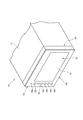
- FIG. 1 is a perspective view of an in-vehicle device employing the electrostatic surge prevention structure of the present invention.
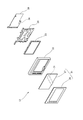
- FIG. 2 is an exploded perspective view showing the display device.
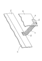
- FIG. 3 is a perspective view showing the flexible printed circuit board and its surroundings.
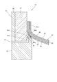
- FIG. 4 is a cross-sectional view showing the touch panel, the flexible printed circuit board, and the periphery thereof.
- FIG. 5 is an explanatory view showing the position and shape of the covering portion on the flexible printed board, FIG. 5 (A) is a view showing the covering portion of the first embodiment, and FIG. 5 (B) is the covering of the second embodiment.
- FIG. 5 is an explanatory view showing the position and shape of the covering portion on the flexible printed board
- FIG. 5 (A) is a view showing the covering portion of the first embodiment
- FIG. 5 (B) is the covering of the second embodiment.
- FIG. 1 is a perspective view of an in-vehicle device 10 employing the electrostatic surge prevention structure of the present invention.
- the in-vehicle device 10 includes a device body 11 having a substantially rectangular parallelepiped shape, and a display device 12 that is provided at a front portion of the device body 11 and that can be touch-operated.
- the in-vehicle device 10 is an in-vehicle electronic device such as an audio device that reproduces a CD, a DVD, or a navigation device that searches for a route to a specified destination, and is embedded in a storage space provided in a vehicle instrument panel or the like. Mounted.
- the display device 12 includes a touch screen 15 that is input by touching a finger at an arbitrary position, and a touch switch unit 16 that performs a predetermined operation by touching the finger at a predetermined position.
- the touch switch unit 16 includes a plurality of touch switches 16a, 16b, 16c, 16d, 16e, and 16f.
- FIG. 2 is an exploded perspective view showing the display device 12.
- the display device 12 includes a touch panel assembly 21, a front case 22, a liquid crystal module 23, a liquid crystal holder 24, and a control printed board 26 in order from the front.
- the touch panel assembly 21 includes a touch panel 27 and a decorative panel 28 attached to the front surface of the touch panel 27.
- the touch panel 27 is a panel that employs a touch detection method such as a resistive film method or a capacitance method that is placed on the front surface of the liquid crystal module 23 and touches the display on the liquid crystal screen of the liquid crystal module 23. A predetermined input operation is performed.
- the decorative panel 28 forms the touch screen 15 and the touch switch unit 16 by being attached to the front surface of the touch panel 27, and covers the pattern of the drive circuit formed on the peripheral portion of the touch panel 27.
- the front case 22 is made of a resin in which the touch panel assembly 21 is attached to the front surface and the liquid crystal module 23, the liquid crystal holder 24, and the control printed board 26 are accommodated inside.
- the liquid crystal module 23 includes a liquid crystal display, a drive circuit board that drives the liquid crystal display, a backlight, and the like.
- the liquid crystal holder 24 holds the liquid crystal module 23 and is attached to the front case 22.
- the control printed board 26 is a board having a touch panel control circuit disposed in the vicinity of the liquid crystal holder 24.
- FIG. 3 is a perspective view showing the flexible printed circuit board 31 and its surroundings.
- a pattern forming portion 27 a on which a conductive line pattern for outputting touched position information is formed is provided at the rear edge of the touch panel 27.
- One end portion 31a of the flexible printed board 31 is connected to the pattern forming portion 27a by adhesion.
- the other end portion 31 b of the flexible printed board 31 is detachably connected to a connector 34 provided on the control printed board 26.
- a signal corresponding to the touch position is sent from the touch panel 27 to the control printed circuit board 26 via the flexible printed circuit board 31, and the touch position is specified.
- FIG. 4 is a cross-sectional view showing the touch panel 27, the flexible printed circuit board 31, and the periphery thereof.
- a gap 41 serving as a part of the design is provided between the touch panel assembly 21 and the front case 22 (or the touch panel 27 and the front case 22). Due to the gap 41, static electricity may enter the display device 12 from a finger touching the touch panel 27 or the decorative panel 28, and may damage an IC or the like provided on the control printed circuit board 26 (see FIG. 3), for example.
- the flexible printed circuit board 31 has the following structure. That is, the flexible printed circuit board 31 covers the base material 42 forming the central layer of the thickness, the conductor portions 43 and 44 made of copper foil or the like provided on both surfaces of the base material, and the conductor portions 43 and 44, respectively. Insulating coatings 46 and 47 are used.
- the base material 42 is made of a resin material such as polyimide.
- the conductor portion 43 is a signal line that allows a signal to flow from the touch panel 27 to the control printed board 26.
- the conductor 44 is connected to the ground on the control printed circuit board 26 (see FIG. 3) side.
- the insulating coatings 46 and 47 are formed of a colorless or colored transparent polyimide film, solder resist film, or the like.
- the insulating coating 47 on the conductor portion 44 side is notched at a position closest to the opening 41 a inside the gap 41 (specifically, the center point 41 b of the opening 41 a) to form a notch portion 47 a, and the conductor portion 44 is formed.
- the exposed portion 44A is exposed to the outside from the notch 47a.
- the exposed portion 44A of the conductor portion 44 By forming the exposed portion 44A of the conductor portion 44 in this way, when static electricity enters the front case 22 from the gap 41, the exposed portion 44A serves as a lightning rod, and induces static electricity to the exposed portion 44A. You can escape to the ground.
- the exposed portion 44A is provided, for example, at a position closer to the gap 41 than a portion where static electricity may be induced, such as an adhesive portion of the flexible printed board 31 to the touch panel 27, and thus the one end portion 31a of the conductor portion 43, etc. It is possible to prevent static electricity from being induced.
- the exposed portion 44A may be formed with a covering portion 51 (a portion subjected to cross-hatching) by performing conductive plating for preventing corrosion.
- a covering portion 51 a portion subjected to cross-hatching
- the plating gold plating or tin plating is suitable. Since the covering portion 51 has conductivity, like the exposed portion 44A, it is a portion that can induce static electricity and is exposed to the outside, and the covering portion 51 constitutes an exposed portion.
- FIG. 5 is an explanatory diagram showing the positions and shapes of the covering portions 51 and 55 on the flexible printed boards 31 and 35.
- FIG. 5A is a view showing the covering portion 51 of the first embodiment
- FIG. 5B is a view showing the covering portion 55 of the second embodiment.
- the notch 47 a is formed so that the insulating coating 47 is stripped in the width direction over the entire width of the flexible printed circuit board 31.
- the notch 47a is formed along the direction in which the gap 41 (see FIG. 4) extends, and the area of the exposed portion 44A (see FIG. 4) (or the covering portion 51) is increased, thereby further inducing static electricity. Can be easier.
- the notch 47 b of the insulating coating 47 is formed in an oval shape extending in the width direction of the flexible printed circuit board 31.
- a covering portion 55 made of plating is provided so as to cover the entire exposed portion (not shown) formed in the conductor portion 44 by the notch portion 47b.
- the shape of the notches 47a and 47b is not limited to the shape described above, and may be a circle, an ellipse, a rectangle, or other shapes. In short, it is only necessary that the conductor portion 44 (or the covering portions 51 and 55) is exposed to the outside and can take in static electricity.
- 41 is provided with a flexible printed circuit board 31 connected to a control printed circuit board 26 serving as a circuit board accommodated in the front case 22 of the display device 12.
- the flexible printed circuit board 31 includes two conductor portions 43, 44, the surfaces of these conductor portions 43, 44 are covered with insulating coatings 46, 47, and the insulating coating 47 is peeled off at a portion facing the gap 41 to expose the conductor portions 44 to the outside.
- a covering portion 51) as an exposed portion is formed, and the conductor portion 44 having the exposed portion 44A is grounded.
- the exposed portion 44A (or the covering portion 51) is provided at a position closer to the gap 41 than an adhesive portion to the touch panel 27 provided at the end portion of the flexible printed circuit board 31, the exposed portion 44A (or By providing the covering portion 51) closer to the gap 41, static electricity can easily reach the exposed portion 44A (covering portion 51) from the gap 41, and the occurrence of electrostatic surge can be prevented.
- conductive plating is applied to the exposed portion 44A (or the covering portion 51)
- corrosion of the exposed portion 44A of the conductor portion 44 can be prevented by plating, and an electrostatic surge is generated over a long period of time. Can be prevented.
- the two members are a front case 22 that constitutes a front portion of the in-vehicle electronic device, and a touch panel 27 (or touch panel assembly) attached to the front case 22.
- the flexible printed circuit board 31 is connected to the touch panel 27 and a touch panel control circuit provided on the control printed circuit board 26, so that an electrostatic surge is generated due to static electricity flowing from an occupant operating the touch panel 27. Can be prevented, and damage to the IC or the like of the touch panel control circuit can be prevented.
Landscapes
- Engineering & Computer Science (AREA)
- Mechanical Engineering (AREA)
- Chemical & Material Sciences (AREA)
- Combustion & Propulsion (AREA)
- Transportation (AREA)
- Microelectronics & Electronic Packaging (AREA)
- Elimination Of Static Electricity (AREA)
- Shielding Devices Or Components To Electric Or Magnetic Fields (AREA)
- Switches That Are Operated By Magnetic Or Electric Fields (AREA)
Abstract
静電サージに対する耐性の向上、コスト及び工数の削減、省スペース化を可能とする静電サージ防止構造を提供する。表示装置(12)に出来た前ケース(22)とタッチパネル組立体(21)との間隙(41)に対応する位置に、前ケース(22)に収納される制御プリント基板に接続されたフレキシブルプリント基板(31)が設けられ、フレキシブルプリント基板(31)は、2層の導体部(43,44)を有し、これらの導体部(43,44)の表面が絶縁被覆(46,47)で覆われ、間隙(41)に対向する部分に絶縁被覆(47)が剥がされて導体部(44)が外部に露出する露出部(44A)(又は露出部としてのめっきによる被覆部(51))が形成され、露出部(44A)(又は被覆部(51))を有する導体部(44)が接地される。
Description
本発明は、車載装置のケースの間隙から入り込む静電気をグランドへ逃がして静電サージの発生を防止することが可能な静電サージ防止構造に関する。
従来、不要な輻射ノイズを吸収する構造を備える車載用の表示装置が知られている(例えば、特許文献1参照)。
表示装置における液晶表示パネルのガラス基板には回路基板部が形成され、回路基板部に設けられたドライバICにフレキシブルプリント基板を介して表示制御装置が接続されている。フレキシブルプリント基板にはシールド用金属箔が貼り付けられ、シールド用金属箔には金属箔テープが貼り付けられ、また、金属箔テープは液晶表示装置の枠体に貼り付けられている。これにより、シールド用金属箔が金属箔テープを介して枠体に電気的に接続されて、フレキシブルプリント基板から発せられる輻射ノイズを吸収する構造が形成されている。
表示装置における液晶表示パネルのガラス基板には回路基板部が形成され、回路基板部に設けられたドライバICにフレキシブルプリント基板を介して表示制御装置が接続されている。フレキシブルプリント基板にはシールド用金属箔が貼り付けられ、シールド用金属箔には金属箔テープが貼り付けられ、また、金属箔テープは液晶表示装置の枠体に貼り付けられている。これにより、シールド用金属箔が金属箔テープを介して枠体に電気的に接続されて、フレキシブルプリント基板から発せられる輻射ノイズを吸収する構造が形成されている。
特許文献1の技術では、例えば、液晶表示パネル側で発生した静電気が液晶表示装置の内部に入り込んで表示制御装置等に備えるICを破損させないようにすることも可能である。静電気をシールド用金属箔、金属箔テープを介してグランド側である枠体に逃がすことができる。
しかしながら、静電気をより逃がしやすい構造として静電サージに対する耐性を向上させることが望まれる。また、特許文献1では、シールド用金属箔や金属箔テープを使用するため、部品点数が増加してコストが増大するとともに、配置スペースの確保が必要になる。また、シールド用金属箔や金属箔テープを貼り付ける部分の洗浄・脱脂の工数が増える。
本発明は、上述した事情を鑑みてなされたものであり、静電サージに対する耐性の向上、コスト及び工数の削減、省スペース化を可能とする静電サージ防止構造を提供することを目的としている。
しかしながら、静電気をより逃がしやすい構造として静電サージに対する耐性を向上させることが望まれる。また、特許文献1では、シールド用金属箔や金属箔テープを使用するため、部品点数が増加してコストが増大するとともに、配置スペースの確保が必要になる。また、シールド用金属箔や金属箔テープを貼り付ける部分の洗浄・脱脂の工数が増える。
本発明は、上述した事情を鑑みてなされたものであり、静電サージに対する耐性の向上、コスト及び工数の削減、省スペース化を可能とする静電サージ防止構造を提供することを目的としている。
この明細書には、2014年7月22日に出願された日本国特許出願・特願2014-148466の全ての内容が含まれる。
上述した課題を解決するため、本発明は、電子機器に出来た2つの部材の間隙に対応する位置に、前記電子機器に収納される基板に接続されたフレキシブルプリント基板が設けられ、当該フレキシブルプリント基板は、2層の導体部を有し、これらの導体部の表面が絶縁被覆で覆われ、前記間隙に対向する部分に前記絶縁被覆が剥がされて前記導体部の一方が外部に露出する露出部が形成され、この露出部を有する前記導体部が接地されることを特徴とする。
上述した課題を解決するため、本発明は、電子機器に出来た2つの部材の間隙に対応する位置に、前記電子機器に収納される基板に接続されたフレキシブルプリント基板が設けられ、当該フレキシブルプリント基板は、2層の導体部を有し、これらの導体部の表面が絶縁被覆で覆われ、前記間隙に対向する部分に前記絶縁被覆が剥がされて前記導体部の一方が外部に露出する露出部が形成され、この露出部を有する前記導体部が接地されることを特徴とする。
この構成によれば、電子機器内に間隙から入り込む静電気を露出部を介してグランドに逃がすことができ、静電サージの発生を防止することができる。既存のフレキシブルプリント基板の導体部を利用して静電気を逃がすため、特別に静電サージを防止する構造及びその構造を設けるための工数、スペースを必要とせず、コスト・工数の削減、省スペース化を図りながら、静電サージに対する耐性を向上させることができる。
上記構成において、前記露出部は、前記フレキシブルプリント基板の端部に設けられた接続部よりも前記間隙に近い位置に設けられていても良い。この構成によれば、露出部を間隙のより近い位置に設けることで、間隙から露出部に静電気を到達し易くすることができ、静電サージの発生を防止することができる。
また、上記構成において、前記露出部に導電性を有するめっきが施されるようにしても良い。この構成によれば、めっきによって露出部の腐食を防止することができる。
また、上記構成において、前記露出部に導電性を有するめっきが施されるようにしても良い。この構成によれば、めっきによって露出部の腐食を防止することができる。
また、上記構成において、前記2つの部材は、車載用の前記電子機器の前部を構成する前ケースと、この前ケースに取付けられたタッチパネルとから構成され、前記フレキシブルプリント基板は、前記タッチパネルと前記基板に設けられたタッチパネル用制御回路とを接続するようにしても良い。この構成によれば、タッチパネルを操作した乗員から流れる静電気による静電サージの発生を防止することができ、タッチパネル用制御回路のIC等の破損を防止することができる。
本発明は、電子機器に出来た2つの部材の間隙に対応する位置に、電子機器に収納される基板に接続されたフレキシブルプリント基板が設けられ、フレキシブルプリント基板は、2層の導体部を有し、これらの導体部の表面が絶縁被覆で覆われ、間隙に対向する部分に絶縁被覆が剥がされて導体部の一方が外部に露出する露出部が形成され、この露出部を有する導体部が接地されるので、電子機器内に間隙から入り込む静電気を露出部を介してグランドに逃がすことができ、静電サージの発生を防止することができる。既存のフレキシブルプリント基板の導体部を利用して静電気を逃がすため、特別に静電サージを防止する構造及びその構造を設けるための工数、スペースを必要とせず、コスト・工数の削減、省スペース化を図りながら、静電サージに対する耐性を向上させることができる。
以下、図面を参照して本発明の実施形態について説明する。
図1は、本発明の静電サージ防止構造を採用した車載装置10の斜視図である。
車載装置10は、略直方体形状の装置本体11と、装置本体11の前部に設けられたタッチ操作可能な表示装置12とを備える。
車載装置10は、CD、DVD等を再生するオーディオ装置、指定された目的地までの経路を探索するナビゲーション装置等の車載用電子機器であり、車両のインストルメントパネル等に設けられる収納スペースに埋め込まれて搭載される。
表示装置12は、指を任意の位置に触れることで入力操作されるタッチ画面15と、指を所定位置に触れることで所定の操作が行われるタッチスイッチ部16とを備える。
タッチスイッチ部16は、複数のタッチスイッチ16a,16b,16c,16d,16e,16fを備える。
図1は、本発明の静電サージ防止構造を採用した車載装置10の斜視図である。
車載装置10は、略直方体形状の装置本体11と、装置本体11の前部に設けられたタッチ操作可能な表示装置12とを備える。
車載装置10は、CD、DVD等を再生するオーディオ装置、指定された目的地までの経路を探索するナビゲーション装置等の車載用電子機器であり、車両のインストルメントパネル等に設けられる収納スペースに埋め込まれて搭載される。
表示装置12は、指を任意の位置に触れることで入力操作されるタッチ画面15と、指を所定位置に触れることで所定の操作が行われるタッチスイッチ部16とを備える。
タッチスイッチ部16は、複数のタッチスイッチ16a,16b,16c,16d,16e,16fを備える。
図2は、表示装置12を示す分解斜視図である。
表示装置12は、手前から順に、タッチパネル組立体21、前ケース22、液晶モジュール23、液晶ホルダ24、制御プリント基板26を備える。
タッチパネル組立体21は、タッチパネル27と、タッチパネル27の前面に貼り付けられる化粧パネル28とを備える。タッチパネル27は、液晶モジュール23の前面に重ね合わされて配置される抵抗膜方式や静電容量方式等のタッチ検出方式が採用されたパネルであり、液晶モジュール23の液晶画面の表示上に触れることで所定の入力操作が行われる。化粧パネル28は、タッチパネル27の前面に貼り付けることでタッチ画面15及びタッチスイッチ部16を形成し、また、タッチパネル27の周縁部に形成された駆動回路のパターンを覆う。
表示装置12は、手前から順に、タッチパネル組立体21、前ケース22、液晶モジュール23、液晶ホルダ24、制御プリント基板26を備える。
タッチパネル組立体21は、タッチパネル27と、タッチパネル27の前面に貼り付けられる化粧パネル28とを備える。タッチパネル27は、液晶モジュール23の前面に重ね合わされて配置される抵抗膜方式や静電容量方式等のタッチ検出方式が採用されたパネルであり、液晶モジュール23の液晶画面の表示上に触れることで所定の入力操作が行われる。化粧パネル28は、タッチパネル27の前面に貼り付けることでタッチ画面15及びタッチスイッチ部16を形成し、また、タッチパネル27の周縁部に形成された駆動回路のパターンを覆う。
前ケース22は、その前面にタッチパネル組立体21が取付けられ、内側に液晶モジュール23、液晶ホルダ24及び制御プリント基板26が収納される樹脂製のものである。
液晶モジュール23は、液晶ディスプレイと、液晶ディスプレイを駆動する駆動回路基板、バックライト等からなる。液晶ホルダ24は、液晶モジュール23を保持し、前ケース22に取付けられる。制御プリント基板26は、液晶ホルダ24に近接して配置されるタッチパネル用制御回路を有する基板である。
液晶モジュール23は、液晶ディスプレイと、液晶ディスプレイを駆動する駆動回路基板、バックライト等からなる。液晶ホルダ24は、液晶モジュール23を保持し、前ケース22に取付けられる。制御プリント基板26は、液晶ホルダ24に近接して配置されるタッチパネル用制御回路を有する基板である。
図3は、フレキシブルプリント基板31及びその周囲を示す斜視図である。
タッチパネル27の背面の縁部には、タッチされた位置情報を出力する導線パターンが形成されたパターン形成部27aが設けられている。パターン形成部27aにはフレキシブルプリント基板31の一端部31aが接着により接続されている。
タッチパネル27の背面の縁部には、タッチされた位置情報を出力する導線パターンが形成されたパターン形成部27aが設けられている。パターン形成部27aにはフレキシブルプリント基板31の一端部31aが接着により接続されている。
フレキシブルプリント基板31は、他端部31bが、制御プリント基板26に設けられたコネクタ34に着脱可能に接続されている。これによって、タッチパネル27からフレキシブルプリント基板31を介して制御プリント基板26にタッチ位置に応じた信号が送られて、タッチ位置が特定される。
図4は、タッチパネル27、フレキシブルプリント基板31、及びその周囲を示す断面図である。
タッチパネル組立体21と前ケース22(又はタッチパネル27と前ケース22)との間には意匠の一部となる間隙41が設けられている。この間隙41によって、タッチパネル27又は化粧パネル28に触れた指から静電気が表示装置12の内部に入り込み、例えば、制御プリント基板26(図3参照)に設けられたIC等を破損させる恐れがある。
タッチパネル組立体21と前ケース22(又はタッチパネル27と前ケース22)との間には意匠の一部となる間隙41が設けられている。この間隙41によって、タッチパネル27又は化粧パネル28に触れた指から静電気が表示装置12の内部に入り込み、例えば、制御プリント基板26(図3参照)に設けられたIC等を破損させる恐れがある。
本実施形態では、フレキシブルプリント基板31を以下に示す構造とすることで、上記の課題を解決している。
即ち、フレキシブルプリント基板31は、厚さの中央の層を形成する基材42と、基材の両面に設けられた銅箔等からなる導体部43,44と、導体部43,44をそれぞれ覆う絶縁被覆46,47とから構成されている。
即ち、フレキシブルプリント基板31は、厚さの中央の層を形成する基材42と、基材の両面に設けられた銅箔等からなる導体部43,44と、導体部43,44をそれぞれ覆う絶縁被覆46,47とから構成されている。
基材42は、ポリイミド等の樹脂材料からなる。導体部43は、タッチパネル27から制御プリント基板26に信号を流す信号線とされている。導体部44は、制御プリント基板26(図3参照)側のグランドに接続されている。
絶縁被覆46,47は、無色又は有色で透明なポリイミド膜、ソルダーレジスト膜等で形成される。
導体部44側の絶縁被覆47は、間隙41の内側の開口41a(詳しくは開口41aの中央の点41b)に最も接近した位置で切り欠かれて切欠き部47aが形成され、導体部44には、切欠き部47aから外部に露出する露出部44Aが出来る。
絶縁被覆46,47は、無色又は有色で透明なポリイミド膜、ソルダーレジスト膜等で形成される。
導体部44側の絶縁被覆47は、間隙41の内側の開口41a(詳しくは開口41aの中央の点41b)に最も接近した位置で切り欠かれて切欠き部47aが形成され、導体部44には、切欠き部47aから外部に露出する露出部44Aが出来る。
このように導体部44の露出部44Aを形成することで、静電気が間隙41から前ケース22内に入り込んだときに、露出部44Aが避雷針の役目をし、静電気を露出部44Aに誘導してグランドに逃がすことができる。露出部44Aは、例えば、タッチパネル27へのフレキシブルプリント基板31の接着部等の静電気が誘導される可能性のある箇所よりも間隙41に近い位置に設けられるため、導体部43の一端部31a等に静電気が誘導されないようにすることができる。
また、露出部44Aには、腐食防止のために導電性を有するめっきを施して被覆部51(クロスハッチングが施された部分である。)を形成しても良い。めっきとしては、金めっき又は錫めっきが好適である。
被覆部51は導電性を有するので、露出部44Aと同じように、静電気を誘導することが可能で且つ外部に露出した部分であり、被覆部51は露出部を構成する。
被覆部51は導電性を有するので、露出部44Aと同じように、静電気を誘導することが可能で且つ外部に露出した部分であり、被覆部51は露出部を構成する。
図5は、フレキシブルプリント基板31,35における被覆部51,55の位置及び形状を示す説明図である。図5(A)は第1実施形態の被覆部51を示す図、図5(B)は第2実施形態の被覆部55を示す図である。
図5(A)に示すように、切欠き部47aは、フレキシブルプリント基板31の幅の全体に亘って絶縁被覆47が幅方向に帯状に剥がされるように形成されている。これにより、切欠き部47aは、間隙41(図4参照)の延びる方向に沿って形成され、露出部44A(図4参照)(又は被覆部51)の面積が大きくなるので、静電気をより誘導しやすくすることができる。
図5(A)に示すように、切欠き部47aは、フレキシブルプリント基板31の幅の全体に亘って絶縁被覆47が幅方向に帯状に剥がされるように形成されている。これにより、切欠き部47aは、間隙41(図4参照)の延びる方向に沿って形成され、露出部44A(図4参照)(又は被覆部51)の面積が大きくなるので、静電気をより誘導しやすくすることができる。
図5(B)に示すように、絶縁被覆47の切欠き部47bは、フレキシブルプリント基板31の幅方向に延びる長円状に形成されている。切欠き部47bによって導体部44に形成された露出部(不図示)の全体を覆うように、めっきからなる被覆部55が設けられている。
切欠き部47a,47b(又は被覆部51,55)の形状は、上記した形状に限らず、円形、楕円形、矩形あるいはその他の形状でも良い。要は導体部44(又は被覆部51,55)が外部に露出し、静電気を取り込むことができれば良い。
以上の図3及び図4に示したように、電子機器としての車載装置10(詳しくは表示装置12)に出来た2つの部材(前ケース22及びタッチパネル組立体21(又はタッチパネル27))の間隙41に対応する位置に、表示装置12の前ケース22に収納される基板としての制御プリント基板26に接続されたフレキシブルプリント基板31が設けられ、フレキシブルプリント基板31は、2層の導体部43,44を有し、これらの導体部43,44の表面が絶縁被覆46,47で覆われ、間隙41に対向する部分に絶縁被覆47が剥がされて導体部44が外部に露出する露出部44A(又は露出部としての被覆部51)が形成され、この露出部44Aを有する導体部44が接地される。
この構成によれば、前ケース22内に間隙41から入り込む静電気を露出部44A(又は被覆部51)を介してグランドに逃がすことができ、静電サージの発生を防止することができる。既存のフレキシブルプリント基板31の導体部44を利用して静電気を逃がすため、特別に静電サージを防止する構造及びその構造を設けるための工数、スペースを必要とせず、コスト・工数の削減、省スペース化を図りながら、静電サージに対する耐性を向上させることができる。
また、露出部44A(又は被覆部51)は、フレキシブルプリント基板31の端部に設けられたタッチパネル27への接着部等よりも間隙41に近い位置に設けられているので、露出部44A(又は被覆部51)を間隙41のより近い位置に設けることで、間隙41から露出部44A(被覆部51)に静電気を到達し易くすることができ、静電サージの発生を防止することができる。
また、露出部44A(又は被覆部51)に導電性を有するめっきが施されるので、めっきによって導体部44の露出部44Aの腐食を防止することができ、長期に亘って静電サージの発生を防止することができる。
また、露出部44A(又は被覆部51)に導電性を有するめっきが施されるので、めっきによって導体部44の露出部44Aの腐食を防止することができ、長期に亘って静電サージの発生を防止することができる。
また、図1、図2及び図3に示したように、2つの部材は、車載用電子機器の前部を構成する前ケース22と、この前ケース22に取付けられたタッチパネル27(又はタッチパネル組立体21)とから構成され、フレキシブルプリント基板31は、タッチパネル27と制御プリント基板26に設けられたタッチパネル用制御回路とを接続するので、タッチパネル27を操作した乗員から流れる静電気による静電サージの発生を防止することができ、タッチパネル用制御回路のIC等の破損を防止することができる。
上述した実施形態は、あくまでも本発明の一態様を示すものであり、本発明の主旨を逸脱しない範囲で任意に変形及び応用が可能である。
10 車載装置(電子機器)
22 前ケース(ケース、部材)
26 制御プリント基板(基板)
27 タッチパネル
31 フレキシブルプリント基板
41 間隙
43,44 導体部
44A 露出部
46,47 絶縁被覆
51,55 被覆部(露出部)
22 前ケース(ケース、部材)
26 制御プリント基板(基板)
27 タッチパネル
31 フレキシブルプリント基板
41 間隙
43,44 導体部
44A 露出部
46,47 絶縁被覆
51,55 被覆部(露出部)
Claims (4)
- 電子機器に出来た2つの部材の間隙に対応する位置に、前記電子機器に収納される基板に接続されたフレキシブルプリント基板が設けられ、
当該フレキシブルプリント基板は、2層の導体部を有し、これらの導体部の表面が絶縁被覆で覆われ、前記間隙に対向する部分に前記絶縁被覆が剥がされて前記導体部の一方が外部に露出する露出部が形成され、この露出部を有する前記導体部が接地されることを特徴とする静電サージ防止構造。 - 前記露出部は、前記フレキシブルプリント基板の端部に設けられた接続部よりも前記間隙に近い位置に設けられていることを特徴とする請求項1に記載の静電サージ防止構造。
- 前記露出部に導電性を有するめっきが施されることを特徴とする請求項1又は2に記載の静電サージ防止構造。
- 前記2つの部材は、車載用の前記電子機器の前部を構成する前ケースと、この前ケースに取付けられたタッチパネルとから構成され、前記フレキシブルプリント基板は、前記タッチパネルと前記基板に設けられたタッチパネル用制御回路とを接続することを特徴とする請求項1乃至3のいずれか一項に記載の静電サージ防止構造。
Priority Applications (3)
| Application Number | Priority Date | Filing Date | Title |
|---|---|---|---|
| US15/317,254 US10559955B2 (en) | 2014-07-22 | 2015-05-28 | Electrostatic surge prevention structure |
| CN201580035099.1A CN106664786B (zh) | 2014-07-22 | 2015-05-28 | 静电浪涌防止构造 |
| EP15823941.8A EP3174372B1 (en) | 2014-07-22 | 2015-05-28 | Electrostatic surge prevention structure |
Applications Claiming Priority (2)
| Application Number | Priority Date | Filing Date | Title |
|---|---|---|---|
| JP2014-148466 | 2014-07-22 | ||
| JP2014148466A JP6396707B2 (ja) | 2014-07-22 | 2014-07-22 | 静電サージ防止構造 |
Publications (1)
| Publication Number | Publication Date |
|---|---|
| WO2016013292A1 true WO2016013292A1 (ja) | 2016-01-28 |
Family
ID=55162828
Family Applications (1)
| Application Number | Title | Priority Date | Filing Date |
|---|---|---|---|
| PCT/JP2015/065373 Ceased WO2016013292A1 (ja) | 2014-07-22 | 2015-05-28 | 静電サージ防止構造 |
Country Status (5)
| Country | Link |
|---|---|
| US (1) | US10559955B2 (ja) |
| EP (1) | EP3174372B1 (ja) |
| JP (1) | JP6396707B2 (ja) |
| CN (1) | CN106664786B (ja) |
| WO (1) | WO2016013292A1 (ja) |
Families Citing this family (5)
| Publication number | Priority date | Publication date | Assignee | Title |
|---|---|---|---|---|
| JP6455154B2 (ja) * | 2015-01-08 | 2019-01-23 | 株式会社デンソー | 車両用電子機器 |
| DE102015016281A1 (de) * | 2015-12-16 | 2017-06-22 | GM Global Technology Operations LLC (n. d. Ges. d. Staates Delaware) | Windschutzscheibe eines Kraftfahrzeugs, System mit Windschutzscheibe sowie Kraftfahrzeug |
| CN108566189A (zh) * | 2018-05-03 | 2018-09-21 | 王汉禄 | 触摸固态开关 |
| CN116600456B (zh) * | 2023-07-18 | 2023-09-08 | 深圳市凯泰精密设备有限公司 | 一种大数据服务器机箱静电防护装置 |
| JP1788616S (ja) * | 2024-05-17 | 2025-01-09 | 車載用モニタ |
Citations (3)
| Publication number | Priority date | Publication date | Assignee | Title |
|---|---|---|---|---|
| JP2001043022A (ja) * | 1999-07-30 | 2001-02-16 | Matsushita Electric Ind Co Ltd | 透明タッチパネルおよびこれを用いた電子機器 |
| JP2009158808A (ja) * | 2007-12-27 | 2009-07-16 | Kyocera Corp | フレキシブル基板及びこれを用いた携帯電子機器 |
| US20140174796A1 (en) * | 2012-12-26 | 2014-06-26 | Canon Kabushiki Kaisha | Flexible printed circuit board and electronic device |
Family Cites Families (8)
| Publication number | Priority date | Publication date | Assignee | Title |
|---|---|---|---|---|
| JP4055672B2 (ja) | 2003-07-31 | 2008-03-05 | 株式会社デンソー | 表示装置 |
| CN2648764Y (zh) | 2003-08-18 | 2004-10-13 | 仁宝电脑工业股份有限公司 | 静电消除装置 |
| JP5026163B2 (ja) | 2007-06-26 | 2012-09-12 | セイコーインスツル株式会社 | 電子機器 |
| CN201788332U (zh) | 2010-08-09 | 2011-04-06 | 东莞通华液晶有限公司 | 可加速静电消散的防静电液晶显示屏 |
| CN202121863U (zh) | 2011-06-16 | 2012-01-18 | 湖北奕宏精密制造有限公司 | 一种抗干扰的柔性电路板 |
| KR102042678B1 (ko) * | 2013-03-25 | 2019-11-11 | 삼성디스플레이 주식회사 | 디스플레이 장치 |
| CN103594022A (zh) | 2013-11-21 | 2014-02-19 | 友达光电(厦门)有限公司 | 显示装置 |
| TWI494822B (zh) * | 2013-12-06 | 2015-08-01 | Au Optronics Corp | 具可撓性電路模組之觸控顯示裝置 |
-
2014
- 2014-07-22 JP JP2014148466A patent/JP6396707B2/ja not_active Expired - Fee Related
-
2015
- 2015-05-28 WO PCT/JP2015/065373 patent/WO2016013292A1/ja not_active Ceased
- 2015-05-28 CN CN201580035099.1A patent/CN106664786B/zh active Active
- 2015-05-28 US US15/317,254 patent/US10559955B2/en active Active
- 2015-05-28 EP EP15823941.8A patent/EP3174372B1/en not_active Not-in-force
Patent Citations (3)
| Publication number | Priority date | Publication date | Assignee | Title |
|---|---|---|---|---|
| JP2001043022A (ja) * | 1999-07-30 | 2001-02-16 | Matsushita Electric Ind Co Ltd | 透明タッチパネルおよびこれを用いた電子機器 |
| JP2009158808A (ja) * | 2007-12-27 | 2009-07-16 | Kyocera Corp | フレキシブル基板及びこれを用いた携帯電子機器 |
| US20140174796A1 (en) * | 2012-12-26 | 2014-06-26 | Canon Kabushiki Kaisha | Flexible printed circuit board and electronic device |
Non-Patent Citations (1)
| Title |
|---|
| See also references of EP3174372A4 * |
Also Published As
| Publication number | Publication date |
|---|---|
| US10559955B2 (en) | 2020-02-11 |
| EP3174372A1 (en) | 2017-05-31 |
| CN106664786A (zh) | 2017-05-10 |
| CN106664786B (zh) | 2018-05-04 |
| EP3174372B1 (en) | 2020-08-05 |
| JP6396707B2 (ja) | 2018-09-26 |
| US20170141566A1 (en) | 2017-05-18 |
| JP2016024961A (ja) | 2016-02-08 |
| EP3174372A4 (en) | 2018-04-11 |
Similar Documents
| Publication | Publication Date | Title |
|---|---|---|
| JP6396707B2 (ja) | 静電サージ防止構造 | |
| JP2014123640A5 (ja) | ||
| JP2013246626A (ja) | タッチパネル及びこれを用いた入力装置 | |
| KR20130084779A (ko) | 터치 패널 | |
| KR101084201B1 (ko) | 액정 표시 장치 | |
| JP7233037B2 (ja) | タッチセンサおよびそれを用いた表示装置 | |
| JP2019505933A (ja) | タッチ導電性フィルム、タッチアセンブリ、タッチディスプレイ及び電子機器 | |
| US10847908B2 (en) | Connected board and display device | |
| JP2011192271A (ja) | タッチスクリーン装置 | |
| JP2015032104A (ja) | タッチパネルセンサ、タッチパネルモジュールおよびタッチパネルセンサの製造方法 | |
| JP6613512B1 (ja) | 電子機器 | |
| JP6147469B2 (ja) | タッチセンサ | |
| JP5814837B2 (ja) | 意匠板およびタッチパネル入力表示機器 | |
| KR101362514B1 (ko) | 터치 키의 정전기 방전 장치 | |
| JP6236892B2 (ja) | 表示装置 | |
| JP2020052210A (ja) | 表示装置 | |
| JP7113664B2 (ja) | パネル構造 | |
| CN107132943B (zh) | 触摸面板传感器以及触摸面板 | |
| TWI581146B (zh) | 觸控面板 | |
| JP6817650B1 (ja) | 電子機器 | |
| KR102237833B1 (ko) | 터치 패널 | |
| JP7205860B2 (ja) | 静電方式の入力装置 | |
| KR102212918B1 (ko) | 터치 패널 | |
| JP4999778B2 (ja) | 静電容量センサ | |
| CN205103514U (zh) | 电子设备 |
Legal Events
| Date | Code | Title | Description |
|---|---|---|---|
| 121 | Ep: the epo has been informed by wipo that ep was designated in this application |
Ref document number: 15823941 Country of ref document: EP Kind code of ref document: A1 |
|
| WWE | Wipo information: entry into national phase |
Ref document number: 15317254 Country of ref document: US |
|
| NENP | Non-entry into the national phase |
Ref country code: DE |
|
| REEP | Request for entry into the european phase |
Ref document number: 2015823941 Country of ref document: EP |
|
| WWE | Wipo information: entry into national phase |
Ref document number: 2015823941 Country of ref document: EP |