WO2016013466A1 - フィルタ - Google Patents
フィルタ Download PDFInfo
- Publication number
- WO2016013466A1 WO2016013466A1 PCT/JP2015/070276 JP2015070276W WO2016013466A1 WO 2016013466 A1 WO2016013466 A1 WO 2016013466A1 JP 2015070276 W JP2015070276 W JP 2015070276W WO 2016013466 A1 WO2016013466 A1 WO 2016013466A1
- Authority
- WO
- WIPO (PCT)
- Prior art keywords
- circuit
- metasurface
- pulse width
- wave
- waveform selection
- Prior art date
- Legal status (The legal status is an assumption and is not a legal conclusion. Google has not performed a legal analysis and makes no representation as to the accuracy of the status listed.)
- Ceased
Links
Images


Classifications
-
- H—ELECTRICITY
- H01—ELECTRIC ELEMENTS
- H01Q—ANTENNAS, i.e. RADIO AERIALS
- H01Q15/00—Devices for reflection, refraction, diffraction or polarisation of waves radiated from an antenna, e.g. quasi-optical devices
- H01Q15/0006—Devices acting selectively as reflecting surface, as diffracting or as refracting device, e.g. frequency filtering or angular spatial filtering devices
-
- G—PHYSICS
- G02—OPTICS
- G02B—OPTICAL ELEMENTS, SYSTEMS OR APPARATUS
- G02B5/00—Optical elements other than lenses
- G02B5/20—Filters
-
- H—ELECTRICITY
- H01—ELECTRIC ELEMENTS
- H01Q—ANTENNAS, i.e. RADIO AERIALS
- H01Q15/00—Devices for reflection, refraction, diffraction or polarisation of waves radiated from an antenna, e.g. quasi-optical devices
- H01Q15/0006—Devices acting selectively as reflecting surface, as diffracting or as refracting device, e.g. frequency filtering or angular spatial filtering devices
- H01Q15/0013—Devices acting selectively as reflecting surface, as diffracting or as refracting device, e.g. frequency filtering or angular spatial filtering devices said selective devices working as frequency-selective reflecting surfaces, e.g. FSS, dichroic plates, surfaces being partly transmissive and reflective
- H01Q15/0026—Devices acting selectively as reflecting surface, as diffracting or as refracting device, e.g. frequency filtering or angular spatial filtering devices said selective devices working as frequency-selective reflecting surfaces, e.g. FSS, dichroic plates, surfaces being partly transmissive and reflective said selective devices having a stacked geometry or having multiple layers
-
- H—ELECTRICITY
- H01—ELECTRIC ELEMENTS
- H01Q—ANTENNAS, i.e. RADIO AERIALS
- H01Q15/00—Devices for reflection, refraction, diffraction or polarisation of waves radiated from an antenna, e.g. quasi-optical devices
- H01Q15/0006—Devices acting selectively as reflecting surface, as diffracting or as refracting device, e.g. frequency filtering or angular spatial filtering devices
- H01Q15/006—Selective devices having photonic band gap materials or materials of which the material properties are frequency dependent, e.g. perforated substrates, high-impedance surfaces
- H01Q15/008—Selective devices having photonic band gap materials or materials of which the material properties are frequency dependent, e.g. perforated substrates, high-impedance surfaces said selective devices having Sievenpipers' mushroom elements
-
- H—ELECTRICITY
- H01—ELECTRIC ELEMENTS
- H01Q—ANTENNAS, i.e. RADIO AERIALS
- H01Q15/00—Devices for reflection, refraction, diffraction or polarisation of waves radiated from an antenna, e.g. quasi-optical devices
- H01Q15/14—Reflecting surfaces; Equivalent structures
-
- H—ELECTRICITY
- H03—ELECTRONIC CIRCUITRY
- H03H—IMPEDANCE NETWORKS, e.g. RESONANT CIRCUITS; RESONATORS
- H03H7/00—Multiple-port networks comprising only passive electrical elements as network components
- H03H7/01—Frequency selective two-port networks
-
- H—ELECTRICITY
- H05—ELECTRIC TECHNIQUES NOT OTHERWISE PROVIDED FOR
- H05K—PRINTED CIRCUITS; CASINGS OR CONSTRUCTIONAL DETAILS OF ELECTRIC APPARATUS; MANUFACTURE OF ASSEMBLAGES OF ELECTRICAL COMPONENTS
- H05K9/00—Screening of apparatus or components against electric or magnetic fields
Definitions
- the present invention relates to a filter having electromagnetic characteristics that enables even radio waves of the same frequency to be selectively absorbed and transmitted according to the waveform of the radio waves.
- the pulse width is the length of radio waves (pulses) in units of time in which radio waves are generated.
- the pulse width is also the length of time (excitation time) during which radio wave energy is generated.
- the electromagnetic field characteristics are determined by the resonance phenomenon of the periodic structure. Even unique electromagnetic field characteristics that cannot be obtained can be obtained.
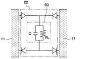
- Non-Patent Documents 1 and 2 have a structure in which a plurality of conductive members having conductivity are periodically arranged in a grid pattern on a planar dielectric using full-wave rectification. Further, as shown in FIG. 24, adjacent conductive members 11 are connected by a full-wave rectifier circuit 22 formed of a diode bridge, and an RC circuit 60 in which a capacitor is connected in parallel with a resistor is included in the full-wave rectifier circuit 22. Have. In addition, this circuit structure is arrange
- the conventional metasurface of FIG. 24 has a characteristic of absorbing a short pulse and transmitting a long pulse even with the same frequency radio wave.
- the operation principle will be described.
- the capacitor has an impedance of 1 / j ⁇ C.
- j is an imaginary unit
- ⁇ 2 ⁇ f (f is a frequency)
- C represents a capacitance.
- the capacitor can store high frequency energy.
- the energy of the low frequency component completely charges the capacitor, and the capacitor cannot store any more energy.
- the energy stored in the capacitor is then released to the resistor. Therefore, a short pulse-width radio wave can dissipate all energy before the next radio wave arrives.
- the incident wave induces a surface current, and here has a frequency component f.
- this frequency component is gradually converted into a DC component by the rectifying action of the diode.
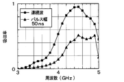
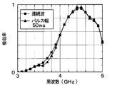
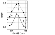
- Non-Patent Documents 1 and 2 list the characteristics shown in FIG. In FIG. 25, the horizontal axis represents the pulse width, the vertical axis represents the absorption rate, the black square represents the simulation result, and the white square represents the experimental result.
- FIG. 25A can be shifted left and right as shown in FIG. 25B by changing the time constant R CC newly specified this time.
- FIG. 25B shows all the simulation results.
- the white circle uses a capacitance 10 times larger than that of the black square (that is, a time constant that is 10 times larger), and the white triangle indicates one-tenth the capacitance of the black square (that is, 10). 1 time constant).
- the waveform selectivity of the conventional example developed by these can change the range of the pulse width absorbed by the time constant, the short pulse always has higher absorption characteristics, and the absorption characteristics of long pulses and continuous waves are Get smaller.
- the conventional example has the following problems. Absorbing a long pulse through a short pulse width signal cannot be obtained from this capacitor and resistor structure. Relatedly, only a signal having an arbitrary pulse width can be absorbed or transmitted, and other signals cannot be transmitted and absorbed, respectively.
- An object of the present invention is to provide a filter having characteristics such that the absorptance increases as the pulse width increases in at least a part of the pulse width region.
- the present inventor has found that the above problem can be solved by adopting the following configuration. That is, according to the present invention, the following filter is provided.
- the filter according to the first aspect is a filter having different radio wave absorption rates depending on radio wave waveforms, and is generated by a conductive member, a rectifier circuit connecting two portions of the conductive member, and a current rectified by the rectifier circuit.
- An RL circuit including an inductor that generates electric power and a resistor that converts current into heat.
- the filter according to the second aspect is a filter with different radio wave absorption rates depending on the waveform of the radio wave, wherein the conductive member, the rectifier circuit connecting the two portions of the conductive member, the inductor and the resistor are connected in series, And a RL circuit through which a current rectified by the rectifier circuit flows.
- the filter according to the first or second aspect it is possible to obtain characteristics such that the absorption rate increases as the pulse width increases in at least a part of the pulse width region.
- FIG. 3 is a diagram illustrating a waveform selection metasurface in which an RL circuit 30 is connected to a full-wave rectifier circuit 22 in the first embodiment. In 1st Embodiment, it is a top view of the waveform selection metasurface which connected the RL circuit 30 to the half-wave rectifier circuits 24a and 24b.
- FIG. 6B is a VIC-VIC sectional view of FIG. 6B.
- the experimental apparatus which measures the absorption factor with respect to the pulse width of a waveform selection metasurface is shown. It is a graph which shows the simulation result and experimental result of the absorption factor with respect to a pulse width. A single time constant is used. It is a graph which shows the simulation result of the absorption factor with respect to a frequency. It is a graph which shows the simulation result and experimental result of the absorption factor with respect to a pulse width. Multiple time constants are used. It is a circuit block diagram of the waveform selection metasurface using full wave rectification based on 2nd Embodiment. It is a block diagram which shows arrangement
- the simulation result and experimental result of the absorptance with respect to the pulse width in 3rd Embodiment are shown. It is a graph which shows the simulation result of the absorption factor with respect to the frequency in 3rd Embodiment. It is the figure which represented simply the mode of the transmitted wave in the time domain at the time of irradiating a metasurface with a continuous wave (surface wave). It is a block diagram of the waveform selection metasurface in 4th Embodiment. It is a circuit diagram of the waveform selection metasurface in 4th Embodiment. It is a figure which shows the transient characteristic of the waveform selection metasurface in 4th Embodiment. It is a block diagram of the waveform selection metasurface in 5th Embodiment.
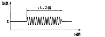
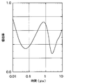
- Pulse width used in this embodiment is defined in FIG. 1A.
- the pulse width is the length of a radio wave (pulse) in a time unit in which radio waves are generated, and is also the length of time in which radio wave energy is continuously generated.
- FIG. 1B shows selective transmission characteristics depending on the pulse width at the same frequency in the waveform selection metasurface of the present embodiment.
- FIG. 1B shows that the waveform selection metasurface (corresponding to a filter) of the present embodiment can transmit radio waves with the same frequency, transmit radio waves with a short pulse width, and absorb radio waves with a long pulse width. Therefore, the waveform selection metasurface is a waveform selection filter and is also an electromagnetic field material having a filter function.
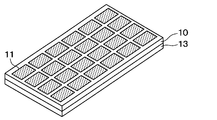
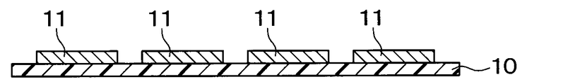
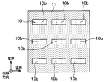
- Fig. 2 shows the overall structure of the waveform selection metasurface.
- the dielectric 10 is provided on the metal plate 13, and has a planar basic shape in which a plurality of conductive members 11 are disposed on the dielectric 10.
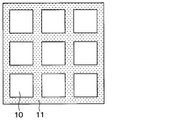
- FIG. 3A, FIG. 3B, and FIG. 3C show an arrangement example with periodicity among variations of the arrangement of the conductive member 11 on the dielectric 10.
- a conductive member 11 having a plurality of quadrangular shapes for example, a square shape having a side of about 18 mm
- a single dielectric material 10 more specifically, a square shape.
- An example of a two-dimensional square lattice shape that is, a matrix shape
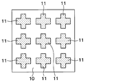
- FIG. 3B shows a checkered pattern in which a plurality of quadrangular holes are formed in a two-dimensional square lattice shape (that is, a matrix shape) on a single dielectric material 10 (more specifically, a square shape).
- a two-dimensional square lattice shape that is, a matrix shape
- a single dielectric material 10 more specifically, a square shape.
- positioned the one electroconductive member 11 is shown.
- the RL circuit 30 and / or the RC circuit 40 is arranged in the dielectric 10.
- FIG. 3C shows an example in which the shape of the conductive member 11 is changed to a cross shape with respect to the example of FIG. 3A.
- the shape of the conductive member 11 is not limited to the example shown in FIGS. 3A to 3C, and various shapes are possible as long as the arrangement can be made periodically.
- the waveform selection metasurface can be made into a planar shape or a flat plate shape by separating and periodically arranging a plurality of conductive members. By making it flat or flat, the waveform selection metasurface can function as an antenna that can receive radio waves efficiently, or it can be stacked on top of an existing antenna to form a waveform selection metasurface. .
- FIG. 4A, 4B, and 4C show variations in the cross-sectional structure of the waveform selection metasurface.
- FIG. 4A shows a basic structure in which a conductive member 11 is disposed on a dielectric 10.
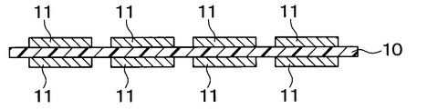
- FIG. 4B shows a structure in which conductive members 11 are arranged on both upper and lower surfaces of the dielectric 10.
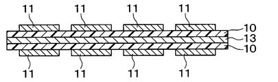
- FIG. 4C shows a structure in which the basic structure of FIG. 4A is stacked. Any of the cross-sectional structures of FIGS. 4A, 4B, and 4C can be combined with any of the arrangements of FIGS. 3A, 3B, and 3C.
- 5A and 5B show a cross-sectional structure of a corrugated selection metasurface having a metal plate 13 lined with a dielectric 10 as a further variation of the cross-sectional structure of the corrugated selection metasurface.
- FIG. 5A shows a basic structure in which a dielectric 10 is laminated on a metal plate 13 and a conductive member 11 is arranged on the dielectric 10.
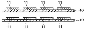
- FIG. 5B shows a structure in which one dielectric 10 is laminated on each of the upper and lower surfaces of the metal plate 13 and the conductive member 11 is disposed on each of the two dielectrics 10.
- selective absorption can be realized on both sides by disposing the dielectric 10 and the conductive member 11 on both sides of the metal plate as shown in FIG. 5B.
- 5A and 5 can be combined with any of the arrangements shown in FIGS. 3A, 3B, and 3C.
- a plurality of conductive members 11 arranged at intervals with a periodicity are formed as shown in FIG. 6A. It is electrically connected via the structure of the rectifier circuit 22.
- a diode bridge is used as an example of such a waveform selection metasurface. Note that full-wave rectification can also be obtained by using a rectifier circuit element or a rectifier circuit structure such as an ideal diode constituted by a transistor or an operational amplifier instead of the diode bridge.
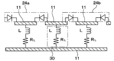
- FIG. 6A and 6B show a waveform selection metasurface in which the RL circuit 30 is connected to the rectifier circuit as the first embodiment.
- FIG. 6A shows a case where the full-wave rectifier circuit 22 is used as the rectifier circuit.
- a full-wave rectifier circuit 22 is formed as a rectifier circuit in the electrical wiring (connection circuit) between the adjacent conductive members 11.
- Some of the full-wave rectifier circuit 22, RL circuit 30 the inductor L and resistor R L is connected in series are connected.
- the full-wave rectifier circuit 22 can be replaced by other full-wave rectifier circuits in addition to the diode bridge.
- the equivalent role is played by using an ideal diode using a transistor or an operational amplifier.
- the inductor L Since the inductor L is connected to the full-wave rectifier circuit 22, the inductor L is not subjected to characteristic deterioration due to a high-frequency signal.
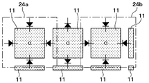
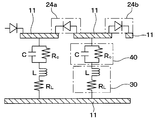
- FIG. 6B and 6C show a waveform selection metasurface using half-wave rectifier circuits 24a and 24b as rectifier circuits.
- FIG. 6B is a plan view of this waveform selection metasurface
- FIG. 6C is a VIC-VIC cross-sectional view of FIG. 6B.
- the electrical wiring (connection circuit) between the uppermost adjacent conductive members 11 in FIG. 6C includes, as a rectifier circuit, a half-wave rectifier circuit 24a that cuts out current outflow from the conductive member 11, and a conductive member. 11 are alternately formed with half-wave rectifier circuits 24b that cut off the current inflow into the circuit 11.
- Half-wave rectifier circuit 24a, to 24b, inductor L and resistor R L are connected in series, the inductors L and resistor R L constitute a RL circuit 30.
- any of the waveform selection metasurfaces of FIGS. 6A, 6B, and 6C various variations as shown in FIGS. 3A to 3C, 4A to 4C, 5A, and 5B are available.
- the dielectric 10 can be disposed.
- the conductive member 11 is periodically arranged on the dielectric 10, and the adjacent conductive member 11 among the conductive members 11 is a rectifier circuit. connecting the wiring meta surfaces (filter), the rectifying circuit, one RL circuit 30 including the resistor R L to convert the inductor L and the current to generate an electromotive force by a current to heat flowing to the other from the conductive member 11 is doing.
- the rectifier circuit is one in which full-wave rectifier circuits 22 or half-wave rectifier circuits 24a or 24b are alternately arranged.
- the waveform selection metasurface of the first embodiment shown in FIGS. 6A to 6C has a feature of transmitting a short pulse and absorbing a long pulse even with the same frequency radio wave.
- the inductor L of the RL circuit 30 has an impedance of j ⁇ L.
- j is an imaginary unit
- ⁇ 2 ⁇ f (f is a frequency)
- L represents an inductance
- the incident wave induces an electric current on the surface of the conductive member.
- the incident wave and the induced current have a frequency component f. Since this frequency component is gradually converted into a DC component by the rectifying action of the diode, a long pulse weakens the electromotive force of the inductor, and its energy is dissipated by the resistor.
- a radio wave having a sufficiently long pulse width is absorbed by the waveform selection metasurface, and a short one is transmitted.
- These characteristics can be controlled by a time constant L / R L (where L is the inductance of the inductor and R L is the resistance value of the resistor).
- FIG. 7 shows an experimental apparatus for measuring the absorption rate with respect to the pulse width of the waveform selection metasurface.
- a sine wave pulse wave is generated from a signal generator.
- the energy E i of the incident wave is measured by a power meter and a power sensor attached to the coupler.
- the energy E r of the reflected wave is also measured.
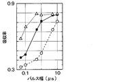
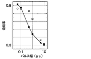
- FIG. 8A shows the simulation result and the experimental result of the absorption rate with respect to the pulse width.
- the simulation is performed under the same conditions as the experiment. Black squares represent simulation results, and white squares represent experimental results. When the pulse width is short, the absorption rate is small, and when the pulse width is long, the absorption rate is large.
- the inductor L has an inductance of 100 ⁇ H
- the resistor RL has a resistance value of 5.5 ohms.
- the frequency of the radio wave was 4.2 GHz in all simulations including this result, and 4.0 GHz in the experiment.
- the frequency (also referred to as the operating frequency) of the radio wave that can obtain an effect such as absorption by the waveform selection metasurface is, for example, the size of the periodic structure of the metal (conductive member 11) on the dielectric (here, 18 mm square). It is possible to operate at different frequencies by changing the square) and the interval.
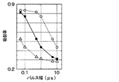
- the absorption rate shown by the black triangle in FIG. 8B is shown.
- the black squares indicate the absorption rate when the radio wave is not a pulse but a continuous wave.
- the frequency range in which waveform selectivity can be obtained depends most strongly on the range in which the full-wave rectifier circuit 22 operates. For example, when a diode using GaAs (gallium arsenide) is used, it can operate at a high frequency such as 20 GHz. Become.
- GaAs gallium arsenide
- FIG. 8C the result of multiplying the inductance by 10 with respect to the simulation of FIG. 8A (black square in FIG. 8C) is shown by a white circle, and the result of reducing the value by 1/10 is shown by a white triangle.
- the absorption rate is small, and when the pulse width is long, the absorption rate is large. Further, the absorption rate A increases as the inductance decreases.
- the RL circuit 30 can obtain a waveform selection metasurface having a characteristic that the absorption rate becomes the minimum value when the pulse width is short and the absorption rate becomes the maximum value when the pulse width is long.
- the characteristics of the waveform selection metasurface having the characteristic that the absorption rate becomes the minimum value when the pulse width is short and the absorption rate becomes the maximum value when the pulse width is long. Can be changed.
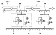
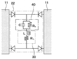
- FIG. 9A, FIG. 9B, and FIG. 9C the RL circuit 30 in which the inductor L and the resistor R are connected in series to the rectifier circuit according to the second embodiment, and the RC circuit 40 in which the capacitor C and the resistor R are connected in parallel are arranged in parallel. Shows the connection.
- FIG. 9A is a circuit configuration diagram of a waveform selection metasurface using full-wave rectification.
- a full-wave rectification circuit 22 is formed as a rectification circuit in the electrical wiring (connection circuit) between the adjacent conductive members 11.
- Some of the full-wave rectifier circuit 22, inductor L and resistor R L is the RL circuit 30 connected in series, an RC circuit 40 to a capacitor C and a resistor R C are connected in parallel, are connected in parallel. Since the inductor L is connected to the full-wave rectifier circuit 22, the inductor L is not subjected to characteristic deterioration due to a high frequency signal.
- 9B and 9C are a configuration diagram and a circuit configuration diagram showing the arrangement of the waveform selection metasurface using half-wave rectification. This is because half-wave rectifier circuits 24 a and 24 b are alternately formed as rectifier circuits in the electrical wiring (connection circuit) between the uppermost adjacent conductive members 11. An RC circuit 40 is connected to the half-wave rectifier circuits 24 a and 24 b in parallel to the RL circuit 30.
- a short pulse that has been absorbed little in the first embodiment can be absorbed by a circuit using the capacitor C.
- intermediate pulse width signals that are not absorbed in both circuit structures can be transmitted.
- the circuit characteristics of the RC circuit 40 can be controlled by a time constant R C C (where C is the capacitance of a capacitor, and R C is the resistance value of a resistor used as a pair with the capacitor), and the characteristics of the inductance circuit structure are also included. Since it can be controlled by the time constant L / R l , any specific waveform can be transmitted and other signals can be absorbed.
- rectification is performed on a metasurface in which conductive members 11 are periodically arranged on the dielectric 10 and adjacent conductive members 11 are wired by a rectifier circuit among the conductive members 11.
- An RC circuit 40 is connected in parallel with the RL circuit 30 in the circuit.
- the rectifier circuit is one in which full-wave rectifier circuits 22 or half-wave rectifier circuits 24a and 24b are alternately arranged.
- the dielectric 10 can be disposed.
- FIG. 10A shows a simulation result and an experimental result of the absorption rate with respect to the pulse width in the second embodiment.
- black squares and black circles show simulation results when different time constants are used, and white circles show experimental results under the same conditions as black circle simulations.
- the black square simulation used a larger capacitance and a smaller inductance than the black circle simulation
- the black circle simulation used a smaller capacitance and a larger inductance than the black square simulation.
- C, L, R C , and RL are 1 nF, 100 ⁇ H, 10 k ⁇ , and 5.5 ⁇ , respectively.
- C, L, and R C 1 and R L are 100 pF, 1 mH, 10 k ⁇ , and 31.2 ⁇ , respectively.
- Other conditions of the simulation and experiment are the same as those in FIGS. 8A to 8C.
- the absorption rate is maximum when the pulse width is long and short, and the absorption rate is minimum when the pulse width is between the long time and the short time, that is, in the middle. Has characteristics.
- the black circle is a combination of a circuit having a small time constant (for example, a white triangle for a black square) in FIG. 25B and a circuit having a large time constant (for example, a white circle for a black square) in FIG. 25B and a circuit having a large time constant (for example, a white circle for a black square) in FIG.
- the RL circuit 30 and the RC circuit 40 are connected in parallel, so that when the pulse width is long and short, the absorption rate becomes the maximum value, and when the pulse width is long and short, A waveform selection metasurface (corresponding to a filter) having the characteristic that the absorptance becomes the minimum value can be formed. Therefore, by changing the time constant of the RL circuit 30 and / or the RC circuit 40, the pulse width at which the absorption rate becomes the maximum value can be set to a desired value.
- FIG. 11A is a circuit configuration diagram of a waveform selection metasurface using full-wave rectification.
- a full-wave rectification circuit 22 is formed as a rectification circuit in the electrical wiring (connection circuit) between the adjacent conductive members 11.
- Some of the full-wave rectifier circuit 22, inductor L and resistor R L is the RL circuit 30 connected in series, an RC circuit 40 to a capacitor C and a resistor R C are connected in parallel, are connected in series. Since the inductor is connected to the full-wave rectifier circuit 22, it is not subject to characteristic deterioration due to a high-frequency signal.
- FIG. 11B is a configuration diagram and a circuit configuration diagram showing the arrangement of the waveform selection metasurface using half-wave rectification.
- half-wave rectifier circuits 24 a and 24 b are alternately formed as rectifier circuits in the electrical wiring (connection circuit) between the uppermost adjacent conductive members 11.
- the RL circuit 30 is connected to the half-wave rectifier circuits 24 a and 24 b, and the RC circuit 40 is connected to the RL circuit 30 in series.
- the long pulse absorbed in the first embodiment can also be transmitted through a circuit using a capacitor.
- intermediate pulse width signals that are not transmitted in both circuit structures can be absorbed.
- the circuit characteristics of the capacitor of the RC circuit 40 can be controlled by the time constant R C C (where C is the capacitance of the capacitor and R C is the resistance value of the resistor used in pairs), and the characteristics of the circuit structure of the RL circuit 30 because it can control the time constant L / R l also, the two time constant by adjusting independently to absorb any particular waveform can be transmitted through the other signals.
- FIG. 12A shows a simulation result and an experimental result of the absorption rate with respect to the pulse width in the third embodiment.
- Black squares and black circles show simulation results when different time constants are used, and white squares show experimental results of black squares.
- the black square used a relatively small capacitance and a large inductance
- the black circle used a relatively large capacitance and a small inductance.
- C, L, R C , and RL are 1 nF, 100 ⁇ H, 10 k ⁇ , and 5.5 ⁇ , respectively.
- C, L, and R C 1 and R L are 10 nF, 10 ⁇ H, 10 k ⁇ , and 2 ⁇ , respectively.
- Other conditions of the simulation and experiment are the same as those in FIGS. 8A to 8C.
- the absorption rate is the minimum value, and when the pulse width is long, the absorption rate has the maximum value when it is between 1 and the short time, that is, in the middle. That is, the black circle is a combination of the circuit having a large time constant (for example, a white circle for a black square) in FIG. 25B and the circuit having a small time constant (for example, a white triangle for the black square) in FIG.
- simulation result and the experimental result in FIG. 12A show that a specific pulse width signal can be absorbed experimentally although there is a difference depending on the parasitic parameter of the circuit used and the DC superposition characteristics of the inductor. .
- the absorption rate becomes the minimum value when the pulse width is long and short, and the time between when the pulse width is long and short.
- a waveform selection metasurface (corresponding to a filter) with the characteristic that the absorption rate becomes the maximum value is created.
- FIG. 13 is a diagram simply showing the state of transmitted waves in the time domain when the metasurface of the present invention is irradiated with continuous waves (surface waves).
- A is a conventional example
- (b) is a first embodiment
- (c) is a second embodiment
- (d) is a third embodiment.
- the portions that appear to be blacked out are actually portions where the waveforms are densely packed.
- Waveform selectivity also has a filtering effect that changes by changing the waveform of incident radio waves.
- (A) shows the transmitted wave in the time domain when a conventional metasurface is irradiated with a continuous wave. Since the metasurface of the conventional example has the characteristics shown in FIGS. 25A and 25B, the absorption rate is large when the pulse width is small, and the absorption rate is small when the pulse width is large. Therefore, the continuous wave is absorbed in the initial state in the time domain and is transmitted when time elapses. In this way, the transmitted wave has a waveform obtained by cutting off the initial energy from the continuous wave.
- (B) shows a transmitted wave in the time domain when the metasurface of the first embodiment is irradiated with a continuous wave. Since the metasurface of the first embodiment has the characteristics shown in FIGS. 8A and 8C, the absorption rate is small when the pulse width is small, and the absorption rate is large when the pulse width is large. Therefore, the continuous wave is transmitted in the initial state in the time domain, and is absorbed as time elapses. Thus, the transmitted wave is a waveform of only the initial energy of the continuous wave.
- (C) shows the transmitted wave in the time domain when the metasurface of the second embodiment is irradiated with a continuous wave. Since the metasurface of the second embodiment has the characteristics shown in FIG. 10A, the absorption rate is large when the pulse width is small and large, and the absorption rate is small when the pulse width is between them. Therefore, in the time domain, the continuous wave is absorbed in the initial state and the state in which time has elapsed, and the pulse width is transmitted at a time corresponding to an intermediate time between them. In this way, the transmitted wave cuts the energy in the state in which the initial and time have passed from the continuous wave, and becomes a waveform of only the time corresponding to the intermediate time of the pulse width.
- (D) shows a transmitted wave in the time domain when the metasurface of the third embodiment is irradiated with a continuous wave. Since the metasurface of the third embodiment has the characteristics shown in FIG. 12A, the absorption rate is small when the pulse width is small and large, and the absorption rate is large when the pulse width is between them. Therefore, the continuous wave is transmitted in the time domain in the initial state and in the state in which time has elapsed, and is absorbed in a time corresponding to the intermediate time of the pulse width. In this way, the transmitted wave is a waveform obtained by cutting off the waveform corresponding to the time when the pulse width is intermediate between them, leaving the energy in the initial state and the time elapsed.
- the rectifier circuit connects the two portions of the conductive member 11 in any of the examples of FIGS. 3A, 3B, and 3B.
- a rectifier circuit connects two adjacent (that is, two) conductive members 11 separated into a plurality.
- the same rectifier circuit is connected to the two places so that the rectifier circuit connects two places of the conductive member 11 that are continuous without being separated.
- the waveform selection metasurface of the present embodiment is a conductive member arranged in a two-dimensional lattice shape (that is, a matrix shape) with respect to the waveform selection metasurface shown in FIG. 3A of the first embodiment. 11 is changed to a vertically long rectangular shape.
- a circuit 30 is arranged.
- the configuration of the RL circuit 30 is the same as that of the first to third embodiments as shown in FIG.
- the propagation direction of the radio wave arriving at the waveform selection metasurface is a direction perpendicular to the paper surface of FIG. 14 and from the front side to the back side of the paper surface. Further, the direction of the electric field vector of the radio wave is the vertical direction on the paper surface, and the direction of the magnetic field vector is the horizontal direction on the paper surface.
- the simulation results of the absorption rate, transmittance, and reflectance of the radio wave in the waveform selection metasurface are as shown in FIG.
- L and RL are 100 ⁇ H and 5.5 ⁇ , respectively.
- a continuous wave is incident on the waveform selection metasurface to be simulated.
- the horizontal axis of the graph of FIG. 16 shows the elapsed time from when the continuous wave of radio waves started to arrive at the waveform selection metasurface, that is, the length of time that the continuous wave has continued to arrive.
- the vertical axis represents the radio wave absorptance in the past predetermined period (specifically, one cycle of continuous wave) from each elapsed time. Therefore, not the averaged absorption characteristic for each pulse width but the transient characteristic in the time domain is evaluated here. However, it is considered that the absorption characteristics with respect to the pulse width tend to be close to this.
- the reflectivity of the waveform selection metasurface for incoming radio waves decreases as the pulse width of the radio waves increases.
- the transmittance of the waveform selection metasurface for incoming radio waves increases as the pulse width of the radio waves increases.
- the absorption rate of the waveform selection metasurface with respect to incoming radio waves tends to be larger when the pulse width of the radio wave is 0.1 ⁇ sec or more than when the pulse width of the radio wave is less than 0.1 ⁇ sec. It is in.
- the waveform selection metasurface of the present embodiment not only the absorptance and transmittance but also the reflectance varies depending on the pulse width of the radio wave. That is, the waveform selection metasurface generally has different scattering characteristics depending on the pulse width of the radio wave.
- the waveform selection metasurface of the present embodiment is a conductive member formed in a two-dimensional lattice shape (that is, a matrix shape) with respect to the waveform selection metasurface shown in FIG. 3B of the first embodiment.
- the shape of the 11 holes is changed to a horizontally long rectangular shape.
- the full-wave rectifier circuit 22 and the RL circuit 30 connected in the full-wave rectifier circuit 22 are disposed in the longitudinal center 10b of each of the plurality of holes in the dielectric 10. Is done.
- the configuration of the RL circuit 30 is the same as that of the first to fourth embodiments as shown in FIG.
- the propagation direction of the radio wave arriving at the waveform selection metasurface is a direction perpendicular to the paper surface of FIG. 17 and from the front side to the back side of the paper surface. Further, the direction of the electric field vector of the radio wave is the vertical direction on the paper surface, and the direction of the magnetic field vector is the horizontal direction on the paper surface.
- the waveform selection metasurface of the present embodiment rotates the waveform selection metasurface of the fourth embodiment by 90 ° around the propagation direction of the radio wave, and further replaces the place where the conductive member 11 is present and the place where the conductive member 11 is not present. Is.
- the scattering characteristics of the radio wave in the waveform selection metasurface of the present embodiment are the same as those obtained by replacing the reflectance and transmittance with respect to the waveform selection metasurface of the fourth embodiment.
- the simulation results of the radio wave absorption rate, transmissivity, and reflectivity in the waveform selection metasurface of the present embodiment are as shown in FIG.
- L and RL are 100 ⁇ H and 5.5 ⁇ , respectively.
- the graph of FIG. 19 is written in the same format as the graph of FIG.
- the transmittance of the waveform selection metasurface for incoming radio waves decreases as the pulse width of the radio waves increases.
- the reflectivity of the waveform selection metasurface for incoming radio waves increases as the pulse width of the radio waves increases.
- the absorption rate of the waveform selection metasurface with respect to incoming radio waves tends to be larger when the pulse width of the radio wave is 0.1 ⁇ sec or more than when the pulse width of the radio wave is less than 0.1 ⁇ sec. It is in.
- the waveform selection metasurface of the present embodiment not only the absorptance and transmittance but also the reflectance varies depending on the pulse width of the radio wave. That is, the waveform selection metasurface generally has different scattering characteristics depending on the pulse width of the radio wave.
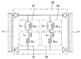
- a first RL circuit 31, a second RL circuit 32, a first RC circuit 41, and a second RC circuit 42 are connected in the full-wave rectifier circuit 22.
- a circuit in which the first RL circuit 31 and the first RC circuit 41 are connected in series, and a circuit in which the second RL circuit 32 and the second RC circuit 42 are connected in series are connected to the full-wave rectifier circuit 22. Connected in parallel.
- the 1RL circuit 31 is a circuit in which the inductor L 1 and a resistor R L1 is connected in series
- first 2RL circuit 32 includes an inductor L 2 and the resistor R L2 is a circuit connected in series.
- the 1RC circuit 41 is a circuit for the capacitor C 1 and resistor R C1 is connected in parallel
- the 2RC circuit 42 is a circuit for the capacitor C 2 and a resistor R C2 is connected in parallel.
- FIG. 21 shows the simulation result of the waveform selection metasurface of this embodiment.
- the values of L 1 , R L1 , L 2 , R L2 , C 1 , R C1 , C 2 , R C2 are 30 ⁇ H, 10 ⁇ , 300 ⁇ H, 10 ⁇ , 30 pF, 10 k ⁇ , 3 nF, 10 k ⁇ , etc. These conditions are the same as in the simulation of the fourth embodiment. Note that the graph of FIG. 21 is described using the same horizontal axis as the graph of FIG.
- the graph of the absorption rate of this waveform selection metasurface is a time chart of a mountain-shaped curve with a high absorption rate at the center, such as the absorption rate of the waveform selection metasurface of the third embodiment (FIG. 12A). Draw two curves arranged in the direction.
- the dependency of the absorption rate on the pulse width can be complicated by combining the RC circuit and the RL circuit in a complicated manner.
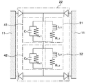
- the waveform selection metasurface of this embodiment is obtained by changing the circuit connected in the full-wave rectifier circuit 22 to the waveform selection metasurface shown in FIG. 6A in the first embodiment.
- a first RL circuit 31, a second RL circuit 32, a first RC circuit 41, and a second RC circuit 42 are connected in the full-wave rectifier circuit 22.
- the internal configuration of these circuits 31, 32, 41, and 42 is the same as in the sixth embodiment.
- a circuit in which the first RL circuit 31 and the first RC circuit 41 are connected in parallel and a circuit in which the second RL circuit 32 and the second RC circuit 42 are connected in parallel are connected to the full-wave rectifier circuit 22. Connected in series.
- FIG. 23 shows a simulation result of the waveform selection metasurface of the present embodiment.
- the values of L 1 , R L1 , L 2 , R L2 , C 1 , R C1 , C 2 , R C2 are 30 ⁇ H, 10 ⁇ , 10 mH, 10 ⁇ , 30 pF, 10 k ⁇ , 1 nF, 10 k ⁇ , etc. These conditions are the same as in the simulation of the sixth embodiment. Note that the graph of FIG. 24 is described using the same horizontal axis as the graph of FIG.
- the graph of the absorption rate of the waveform selection metasurface shows a valley-shaped curve with a low absorption rate in the center, like the absorption rate of the waveform selection metasurface of the second embodiment (FIG. 10A). Draw two curves arranged in the direction.
- the dependency of the absorption rate on the pulse width can be complicated by combining the RC circuit and the RL circuit in a complicated manner.
- the waveform selection metasurface has been described as having different scattering characteristics depending on the pulse width of the radio wave. This is the case with the first to third embodiments, the sixth and the sixth embodiments. This also applies to the seventh embodiment. That is, in the waveform selection metasurfaces of the first to third embodiments, the sixth embodiment, and the seventh embodiment, the reflectance of the radio wave changes when the pulse width of the incoming radio wave changes.
- Modification 2 The resistance value of the resistor, the capacitance of the capacitor, and the inductance of the inductor used in the first to seventh embodiments may be variable. In this case, the time constants of the RL circuit and RC circuit used in the first to seventh embodiments are also variable.
- the resistors of the first to seventh embodiments are not limited to elements that function as a single resistor, but may be a part that realizes a resistance component in an element having a resistance component.
- an element having a resistance component for example, there is a MOSFET in which a drain current is variable when a voltage between the drain and the source is changed by generating a resistance component according to a voltage between the drain and the source.
- the capacitors of the first to seventh embodiments are not limited to elements that function as a single capacitor, but may be a part that realizes a capacitance component in an element having a capacitance component (for example, a variable gap diode).
- the inductors of the first to seventh embodiments are not limited to elements that function as a single inductor, but may be a part that realizes a capacitance component in an element having an inductance component.
- the filters (waveform selection metasurfaces) of the first to seventh embodiments and modifications the effect of obtaining higher absorption characteristics for a long pulse width even with the same frequency radio wave. There is. In addition, it is possible to obtain characteristics such that the absorption rate increases as the pulse width increases, in at least a part of the pulse width region.
- the filter can be made into a planar shape by separating and periodically arranging a plurality of conductive members.
- an antenna that can efficiently receive radio waves can be configured.
- the first to third embodiments it is possible to absorb a long pulse width signal and arbitrarily transmit or absorb a pulse width signal positioned between a short pulse and a long pulse.
- Possible waveform selection can provide a filter. Therefore, according to the present invention, an apparatus can be selected that selects the same frequency by the waveform (pulse width).
- the frequency resource can be expanded two-dimensionally, and the frequency depletion of the radio communication technology It is a fundamental solution to the problem.
- the circuit composed of the RL circuit 30 and the RC circuit 40 connected in series with the full-wave rectifier circuit 22 corresponds to an example of a connection circuit that electrically connects adjacent conductive members.
- the waveform selection metasurface of the above embodiment can be used by giving a “pulse width” that gives a new degree of freedom to existing wireless communication devices and applications such as antennas, and thus can solve the problem of frequency resource depletion. Increases nature.
Landscapes
- Physics & Mathematics (AREA)
- Optics & Photonics (AREA)
- General Physics & Mathematics (AREA)
- Electromagnetism (AREA)
- Engineering & Computer Science (AREA)
- Microelectronics & Electronic Packaging (AREA)
- Shielding Devices Or Components To Electric Or Magnetic Fields (AREA)
- Aerials With Secondary Devices (AREA)
- Filters And Equalizers (AREA)
- Semiconductor Integrated Circuits (AREA)
Abstract
Description
図6A、図6Bに、第1実施形態として、整流回路にRL回路30を接続した波形選択メタサーフェスを示す。図6Aは、整流回路として全波整流回路22を用いる場合を示す。図6Aでは、隣り合う導電性部材11の間の電気配線(接続回路)には、整流回路として全波整流回路22が形成されている。全波整流回路22の中に、インダクタLと抵抗RLが直列に接続したRL回路30が接続されている。ここで、上述のようにこの全波整流回路22は、ダイオードブリッジだけでなく、その他の全波整流回路によって置き換えることが可能である。例えばトランジスタやオペアンプを使用した理想ダイオードを使用することで同等の役割が果たされる。
図9A、図9B、図9Cに、第2実施形態である整流回路にインダクタLと抵抗Rが直列に接続されたRL回路30とコンデンサCと抵抗Rが並列に接続されたRC回路40を並列に接続したものを示す。
図11A、図11B、図11Cに、第3実施形態である整流回路にインダクタLと抵抗RLが直列に接続されたRL回路30とコンデンサCと抵抗RCが並列に接続されたRC回路40を直列に接続した波形選択メタサーフェスを示す。
図13は、本発明等のメタサーフェスに、連続波(表面波)を照射した際の時間領域における透過波の様子を簡易的に表した図である。(a)は従来例、(b)は第1実施形態、(c)は第2実施形態、(d)は第3実施形態を示す。図13の各グラフ中、黒く塗り潰されているように見える部分は、実際には波形が密集している部分である。
次に第4実施形態について、図14~図16を用いて説明する。本実施形態の波形選択メタサーフェスは、図14に示す通り、第1実施形態の図3Aに示した波形選択メタサーフェスに対し、2次元格子状(すなわち、マトリックス状)に配置された導電性部材11の各々の形状を縦長の矩形形状に変更したものである。
次に第5実施形態について、図17~図19を用いて説明する。本実施形態の波形選択メタサーフェスは、図17に示す通り、第1実施形態の図3Bに示した波形選択メタサーフェスに対し、二次元格子状(すなわち、マトリックス状)に形成された導電性部材11の穴の形状を横長の矩形形状に変更したものである。
次に第6実施形態について、図20、図21を用いて説明する。本実施形態の波形選択メタサーフェスは、第1実施形態で図6Aに示した波形選択メタサーフェスに対して、全波整流回路22の中に接続される回路を変更したものである。
次に第7実施形態について、図22、図23を用いて説明する。本実施形態の波形選択メタサーフェスは、第1実施形態で図6Aに示した波形選択メタサーフェスに対して、全波整流回路22の中に接続される回路を変更したものである。
なお、本発明は上記した実施形態に限定されるものではなく、以下の変形例のうち任意の組み合わせを、上記実施形態に適用することができる。
上記第4、第5実施形態において、波形選択メタサーフェスは、散乱特性全般が、電波のパルス幅に応じて異なると説明したが、このことは、第1~第3実施形態、第6、第7実施形態にも当てはまる。つまり、第1~第3実施形態、第6、第7実施形態の波形選択メタサーフェスも、到来する電波のパルス幅が変化すると当該電波の反射率が変化する。
上記第1~第7実施形態において用いられる抵抗の抵抗値、コンデンサのキャパシタンス、インダクタのインダクタンスは、それぞれ、可変であってもよい。この場合、上記第1~第7実施形態において用いられるRL回路およびRC回路の時定数も、可変となる。
また、上記第1~第7実施形態の抵抗は、抵抗単体として機能する素子に限らず、抵抗成分を有する素子中の抵抗成分を実現する部分であってもよい。抵抗成分を有する素子としては、例えば、ドレインとソースの間の電圧に応じた抵抗成分を発生することで、ドレインとソースの間の電圧が変化するとドレイン電流が可変になるMOSFETがある。
(まとめ)
以上の通り、第1~第7実施形態および変形例のフィルタ(波形選択メタサーフェス)の一部またはすべてのフィルタによれば、同一周波数電波でも長いパルス幅に対してより高い吸収特性を得る効果がある。また、パルス幅が長くなるほど吸収率が上昇するような特性を少なくとも一部のパルス幅領域で得ることができる。
Claims (7)
- 電波の波形によって電波の吸収率が異なるフィルタであって、
導電性部材と、
前記導電性部材の2箇所を繋ぐ整流回路と、
前記整流回路によって整流された電流により起電力を発生させるインダクタと前記電流を熱に変換する抵抗とを含むRL回路と、を備えたフィルタ。 - 電波の波形によって電波の吸収率が異なるフィルタであって、
導電性部材と、
前記導電性部材の2箇所を繋ぐ整流回路と、
インダクタと抵抗が直列に接続され、前記整流回路によって整流された電流が流れるRL回路と、を備えたフィルタ。 - 前記RL回路の時定数が可変になっていることで、電波のパルス幅に対する吸収特性の依存性を操作することが可能であることを特徴とする請求項1または2に記載のフィルタ。
- コンデンサと抵抗が並列に接続されたRC回路を備え、
前記RC回路は、前記RL回路と並列に接続することを特徴とする請求項1ないし3のいずれか1つに記載のフィルタ。 - コンデンサと抵抗が並列に接続されたRC回路を備え、
前記RC回路は、前記RL回路と直列に接続することを特徴とする請求項1ないし3のいずれか1つに記載のフィルタ。 - 前記RC回路の時定数が可変になっていることで、電波のパルス幅に対する吸収特性の依存性を操作することが可能であることを特徴とする請求項4または5に記載のフィルタ。
- 前記導電性部材は、複数個に分離して周期的に配置されていることを特徴とする請求項1ないし6のいずれか1つに記載のフィルタ。
Priority Applications (3)
| Application Number | Priority Date | Filing Date | Title |
|---|---|---|---|
| EP15825141.3A EP3174202B1 (en) | 2014-07-22 | 2015-07-15 | Filter |
| US15/327,243 US10741927B2 (en) | 2014-07-22 | 2015-07-15 | Filter |
| JP2016535895A JP6663607B2 (ja) | 2014-07-22 | 2015-07-15 | 波形選択メタサーフェス |
Applications Claiming Priority (6)
| Application Number | Priority Date | Filing Date | Title |
|---|---|---|---|
| JP2014148464 | 2014-07-22 | ||
| JP2014-148464 | 2014-07-22 | ||
| JP2014154363 | 2014-07-30 | ||
| JP2014-154363 | 2014-07-30 | ||
| JP2014253858 | 2014-12-16 | ||
| JP2014-253858 | 2014-12-16 |
Publications (1)
| Publication Number | Publication Date |
|---|---|
| WO2016013466A1 true WO2016013466A1 (ja) | 2016-01-28 |
Family
ID=55162992
Family Applications (1)
| Application Number | Title | Priority Date | Filing Date |
|---|---|---|---|
| PCT/JP2015/070276 Ceased WO2016013466A1 (ja) | 2014-07-22 | 2015-07-15 | フィルタ |
Country Status (4)
| Country | Link |
|---|---|
| US (1) | US10741927B2 (ja) |
| EP (1) | EP3174202B1 (ja) |
| JP (1) | JP6663607B2 (ja) |
| WO (1) | WO2016013466A1 (ja) |
Cited By (4)
| Publication number | Priority date | Publication date | Assignee | Title |
|---|---|---|---|---|
| JP2016119646A (ja) * | 2014-12-19 | 2016-06-30 | 国立大学法人 名古屋工業大学 | 波形選択フィルタを用いた通話システム、通信端末 |
| WO2019221120A1 (ja) * | 2018-05-15 | 2019-11-21 | 浜松ホトニクス株式会社 | 反射型動的メタサーフェス |
| WO2019221133A1 (ja) * | 2018-05-15 | 2019-11-21 | 浜松ホトニクス株式会社 | 発光デバイス |
| CN114069246A (zh) * | 2021-12-02 | 2022-02-18 | 四川大学 | 一种基于周期结构的吸收电磁波的整流表面 |
Citations (1)
| Publication number | Priority date | Publication date | Assignee | Title |
|---|---|---|---|---|
| JP2013030952A (ja) * | 2011-07-28 | 2013-02-07 | Teramikros Inc | エレクトロマグネティック・バンド・ギャップ構造体及びその製造方法 |
Family Cites Families (6)
| Publication number | Priority date | Publication date | Assignee | Title |
|---|---|---|---|---|
| JPS5323248A (en) * | 1976-08-16 | 1978-03-03 | Oki Electric Ind Co Ltd | Variable equivalent circuit network |
| JPS6339207A (ja) * | 1986-08-04 | 1988-02-19 | Nec Corp | 周波数振幅特性の等化器 |
| JP3177437B2 (ja) * | 1996-03-25 | 2001-06-18 | 三洋電機株式会社 | 中間周波同調回路 |
| KR100692204B1 (ko) | 2004-11-26 | 2007-03-09 | (주) 엠큐브테크놀로지 | 완충용 인덕터 기능을 수행할 수 있는 변압기를 구비한전기 회로 및 이를 이용한 자기 자극기 |
| JP4637020B2 (ja) * | 2006-01-05 | 2011-02-23 | 古野電気株式会社 | タンク回路付高周波回路モジュール |
| JP2015025791A (ja) * | 2013-07-29 | 2015-02-05 | 株式会社アドバンテスト | インピーダンス測定装置 |
-
2015
- 2015-07-15 EP EP15825141.3A patent/EP3174202B1/en active Active
- 2015-07-15 JP JP2016535895A patent/JP6663607B2/ja active Active
- 2015-07-15 WO PCT/JP2015/070276 patent/WO2016013466A1/ja not_active Ceased
- 2015-07-15 US US15/327,243 patent/US10741927B2/en active Active
Patent Citations (1)
| Publication number | Priority date | Publication date | Assignee | Title |
|---|---|---|---|---|
| JP2013030952A (ja) * | 2011-07-28 | 2013-02-07 | Teramikros Inc | エレクトロマグネティック・バンド・ギャップ構造体及びその製造方法 |
Non-Patent Citations (1)
| Title |
|---|
| H. WAKATSUCHI ET AL.: "Experimental Demonstration of Nonlinear Waveform-Dependent Metasurface Absorber with Pulsed Signals", ELECTRONICS LETTERS, vol. 49, no. 24, November 2013 (2013-11-01), pages 1530 - 1531, XP055389582 * |
Cited By (9)
| Publication number | Priority date | Publication date | Assignee | Title |
|---|---|---|---|---|
| JP2016119646A (ja) * | 2014-12-19 | 2016-06-30 | 国立大学法人 名古屋工業大学 | 波形選択フィルタを用いた通話システム、通信端末 |
| WO2019221120A1 (ja) * | 2018-05-15 | 2019-11-21 | 浜松ホトニクス株式会社 | 反射型動的メタサーフェス |
| JP2019200251A (ja) * | 2018-05-15 | 2019-11-21 | 浜松ホトニクス株式会社 | 反射型動的メタサーフェス |
| WO2019221133A1 (ja) * | 2018-05-15 | 2019-11-21 | 浜松ホトニクス株式会社 | 発光デバイス |
| JP7144188B2 (ja) | 2018-05-15 | 2022-09-29 | 浜松ホトニクス株式会社 | 反射型動的メタサーフェス |
| US11971643B2 (en) | 2018-05-15 | 2024-04-30 | Hamamatsu Photonics K.K. | Reflective dynamic metasurface |
| US12046874B2 (en) | 2018-05-15 | 2024-07-23 | Hamamatsu Photonics K.K. | Light-emitting device |
| CN114069246A (zh) * | 2021-12-02 | 2022-02-18 | 四川大学 | 一种基于周期结构的吸收电磁波的整流表面 |
| CN114069246B (zh) * | 2021-12-02 | 2023-04-07 | 四川大学 | 一种基于周期结构的吸收电磁波的整流表面 |
Also Published As
| Publication number | Publication date |
|---|---|
| EP3174202A4 (en) | 2018-03-14 |
| JPWO2016013466A1 (ja) | 2017-06-01 |
| EP3174202A1 (en) | 2017-05-31 |
| JP6663607B2 (ja) | 2020-03-13 |
| EP3174202B1 (en) | 2019-10-30 |
| US20170201029A1 (en) | 2017-07-13 |
| US10741927B2 (en) | 2020-08-11 |
Similar Documents
| Publication | Publication Date | Title |
|---|---|---|
| Wang et al. | Observation of nonreciprocal wave propagation in a dynamic phononic lattice | |
| JP6663607B2 (ja) | 波形選択メタサーフェス | |
| Zheng et al. | A piezo-metastructure with bistable circuit shunts for adaptive nonreciprocal wave transmission | |
| Aridogan et al. | Analytical modeling and experimental validation of a structurally integrated piezoelectric energy harvester on a thin plate | |
| Beck et al. | The power output and efficiency of a negative capacitance shunt for vibration control of a flexural system | |
| Mosquera-Sánchez et al. | Dynamics and wave propagation in nonlinear piezoelectric metastructures | |
| JP4538594B2 (ja) | 信号伝達システム | |
| Wu et al. | Wideband energy harvesting based on mixed connection of piezoelectric oscillators | |
| US20050195051A1 (en) | Systems and methods for blocking microwave propagation in parallel plate structures | |
| Liu et al. | Broadband vibration suppression of graded/disorder piezoelectric metamaterials | |
| Lossouarn et al. | Multimodal coupling of periodic lattices and application to rod vibration damping with a piezoelectric network | |
| Maugan et al. | Enhancement of energy harvesting using acoustical-black-hole-inspired wave traps | |
| Qian et al. | Design of a Dual‐Band Waveform‐Selective Metasurface Absorber Based on the Combination of Two Resonator Structures Loaded with Nonlinear Circuits | |
| JP2021034908A5 (ja) | ||
| Liu et al. | Tunable reflection and broadband absorption of flexural waves by adaptive elastic metasurface with piezoelectric shunting circuits | |
| Nguyen et al. | Analytical coupled modeling of a magneto-based acoustic metamaterial harvester | |
| Černík et al. | Sound reflection in an acoustic impedance tube terminated with a loudspeaker shunted by a negative impedance converter | |
| Bao et al. | Electron–phonon metamaterial featuring nonlinear tri-interleaved piezoelectric topologies and its application in low-frequency vibration control | |
| EA028829B1 (ru) | Фотоэлектрический элемент для использования в энергетике | |
| Dong et al. | General formulation of unconditionally stable ADI-FDTD method in linear dispersive media | |
| JP2015534268A5 (ja) | ||
| JP2009225159A (ja) | 電磁波反射面 | |
| Saikia et al. | A polarization‐insensitive time‐modulated frequency‐selective surface for broad frequency range | |
| Hosseinkhani et al. | Multi-functional periodically heterogeneous structures for energy harvesting and vibration attenuation-effects of piezoelectricity and shunting circuits | |
| Wang et al. | A periodic piezoelectric smart structure with the integrated passive/active vibration-reduction performances |
Legal Events
| Date | Code | Title | Description |
|---|---|---|---|
| 121 | Ep: the epo has been informed by wipo that ep was designated in this application |
Ref document number: 15825141 Country of ref document: EP Kind code of ref document: A1 |
|
| ENP | Entry into the national phase |
Ref document number: 2016535895 Country of ref document: JP Kind code of ref document: A |
|
| WWE | Wipo information: entry into national phase |
Ref document number: 15327243 Country of ref document: US |
|
| NENP | Non-entry into the national phase |
Ref country code: DE |
|
| REEP | Request for entry into the european phase |
Ref document number: 2015825141 Country of ref document: EP |
|
| WWE | Wipo information: entry into national phase |
Ref document number: 2015825141 Country of ref document: EP |