WO2016013533A1 - 電荷輸送性材料 - Google Patents
電荷輸送性材料 Download PDFInfo
- Publication number
- WO2016013533A1 WO2016013533A1 PCT/JP2015/070637 JP2015070637W WO2016013533A1 WO 2016013533 A1 WO2016013533 A1 WO 2016013533A1 JP 2015070637 W JP2015070637 W JP 2015070637W WO 2016013533 A1 WO2016013533 A1 WO 2016013533A1
- Authority
- WO
- WIPO (PCT)
- Prior art keywords
- group
- charge transporting
- carbon atoms
- substituted
- bis
- Prior art date
- Legal status (The legal status is an assumption and is not a legal conclusion. Google has not performed a legal analysis and makes no representation as to the accuracy of the status listed.)
- Ceased
Links
- KUBSCXXKQGDPPD-UHFFFAOYSA-N Brc(cc1)cc(c2c3cccc2)c1[n]3-c1ccccc1 Chemical compound Brc(cc1)cc(c2c3cccc2)c1[n]3-c1ccccc1 KUBSCXXKQGDPPD-UHFFFAOYSA-N 0.000 description 1
- CUUYUQPYUVQMBQ-UHFFFAOYSA-N CC(C)(C)c1ccc(C(C)(C)Nc2cc(c3ccccc3cc3)c3cc2)cc1 Chemical compound CC(C)(C)c1ccc(C(C)(C)Nc2cc(c3ccccc3cc3)c3cc2)cc1 CUUYUQPYUVQMBQ-UHFFFAOYSA-N 0.000 description 1
- GXHUSHPXAGEBGP-UHFFFAOYSA-N CC(C)(C)c1ccc(C(C)(C)Nc2cc3cc(cccc4)c4cc3cc2)cc1 Chemical compound CC(C)(C)c1ccc(C(C)(C)Nc2cc3cc(cccc4)c4cc3cc2)cc1 GXHUSHPXAGEBGP-UHFFFAOYSA-N 0.000 description 1
- KVYCEYSWTGVBHA-UHFFFAOYSA-N CC(C)(C)c1ccc(C(C)(C)Nc2cc3ccccc3cc2)cc1 Chemical compound CC(C)(C)c1ccc(C(C)(C)Nc2cc3ccccc3cc2)cc1 KVYCEYSWTGVBHA-UHFFFAOYSA-N 0.000 description 1
- YIGXRTSSRNTIRY-UHFFFAOYSA-N CC(C)(C)c1ccc(C(C)(C)Nc2cccc3c2c2ccccc2cc3)cc1 Chemical compound CC(C)(C)c1ccc(C(C)(C)Nc2cccc3c2c2ccccc2cc3)cc1 YIGXRTSSRNTIRY-UHFFFAOYSA-N 0.000 description 1
- UURIVMFZPNVGHX-UHFFFAOYSA-N CC(C)(C)c1ccc(C(C)(C)Nc2cccc3c2cc(cccc2)c2c3)cc1 Chemical compound CC(C)(C)c1ccc(C(C)(C)Nc2cccc3c2cc(cccc2)c2c3)cc1 UURIVMFZPNVGHX-UHFFFAOYSA-N 0.000 description 1
- VVYWUQOTMZEJRJ-UHFFFAOYSA-N CNc(cc1)ccc1N Chemical compound CNc(cc1)ccc1N VVYWUQOTMZEJRJ-UHFFFAOYSA-N 0.000 description 1
- ROTKCJXMBQLEEV-UHFFFAOYSA-N Cc(cc1)ccc1N(c1ccccc1)c1cccc2c1cccc2 Chemical compound Cc(cc1)ccc1N(c1ccccc1)c1cccc2c1cccc2 ROTKCJXMBQLEEV-UHFFFAOYSA-N 0.000 description 1
- VJTIVALWGKVECS-UHFFFAOYSA-N N#Cc(c(F)c(c(F)c1F)Oc2cc(S(O)(=O)=O)cc3c2ccc(S(O)(=O)=O)c3)c1C#N Chemical compound N#Cc(c(F)c(c(F)c1F)Oc2cc(S(O)(=O)=O)cc3c2ccc(S(O)(=O)=O)c3)c1C#N VJTIVALWGKVECS-UHFFFAOYSA-N 0.000 description 1
- MYWCNXVEFGFTHM-UHFFFAOYSA-N N#Cc(c(F)c(c(Oc1cc(S(O)(=O)=O)cc2c1ccc(S(O)(=O)=O)c2)c1F)F)c1F Chemical compound N#Cc(c(F)c(c(Oc1cc(S(O)(=O)=O)cc2c1ccc(S(O)(=O)=O)c2)c1F)F)c1F MYWCNXVEFGFTHM-UHFFFAOYSA-N 0.000 description 1
- RUFPHBVGCFYCNW-UHFFFAOYSA-N Nc1cccc2c1cccc2 Chemical compound Nc1cccc2c1cccc2 RUFPHBVGCFYCNW-UHFFFAOYSA-N 0.000 description 1
- PAYRUJLWNCNPSJ-UHFFFAOYSA-N Nc1ccccc1 Chemical compound Nc1ccccc1 PAYRUJLWNCNPSJ-UHFFFAOYSA-N 0.000 description 1
- 0 OS(c(cc1)cc2c1c(Oc(c(F)c(c(*C(F)=C(F)F)c1F)F)c1F)cc(S(O)(=O)=O)c2)(=O)=O Chemical compound OS(c(cc1)cc2c1c(Oc(c(F)c(c(*C(F)=C(F)F)c1F)F)c1F)cc(S(O)(=O)=O)c2)(=O)=O 0.000 description 1
- GYWUCUDMYBVQAW-UHFFFAOYSA-N OS(c(cc1)cc2c1c(Oc(c(F)c(c(C(F)(F)F)c1F)F)c1F)cc(S(O)(=O)=O)c2)(=O)=O Chemical compound OS(c(cc1)cc2c1c(Oc(c(F)c(c(C(F)(F)F)c1F)F)c1F)cc(S(O)(=O)=O)c2)(=O)=O GYWUCUDMYBVQAW-UHFFFAOYSA-N 0.000 description 1
- GVLDSAXNCTVTFO-UHFFFAOYSA-N OS(c1cc(ccc(Oc(c(F)c(c(-c(c(F)c(c(Oc(cc2)cc(c(S(O)(=O)=O)c3)c2cc3S(O)(=O)=O)c2F)F)c2F)c2F)F)c2F)c2)c2c(S(O)(=O)=O)c1)(=O)=O Chemical compound OS(c1cc(ccc(Oc(c(F)c(c(-c(c(F)c(c(Oc(cc2)cc(c(S(O)(=O)=O)c3)c2cc3S(O)(=O)=O)c2F)F)c2F)c2F)F)c2F)c2)c2c(S(O)(=O)=O)c1)(=O)=O GVLDSAXNCTVTFO-UHFFFAOYSA-N 0.000 description 1
- JLZFEGXWBXAFIQ-UHFFFAOYSA-N OS(c1cc2cc(S(O)(=O)=O)cc(Oc(c(F)c(c(-c(c(F)c(c(Oc3cc(S(O)(=O)=O)cc4c3ccc(S(O)(=O)=O)c4)c3F)F)c3F)c3F)F)c3F)c2cc1)(=O)=O Chemical compound OS(c1cc2cc(S(O)(=O)=O)cc(Oc(c(F)c(c(-c(c(F)c(c(Oc3cc(S(O)(=O)=O)cc4c3ccc(S(O)(=O)=O)c4)c3F)F)c3F)c3F)F)c3F)c2cc1)(=O)=O JLZFEGXWBXAFIQ-UHFFFAOYSA-N 0.000 description 1
- JXCKDZQFJXBSLR-UHFFFAOYSA-N c(cc1)ccc1-[n]1c(ccc(N(c(cc2)ccc2N(c(cc2)cc(c3ccccc33)c2[n]3-c2ccccc2)c(cc2)cc(c3ccccc33)c2[n]3-c2ccccc2)c(cc2)cc(c3ccccc33)c2[n]3-c2ccccc2)c2)c2c2c1cccc2 Chemical compound c(cc1)ccc1-[n]1c(ccc(N(c(cc2)ccc2N(c(cc2)cc(c3ccccc33)c2[n]3-c2ccccc2)c(cc2)cc(c3ccccc33)c2[n]3-c2ccccc2)c(cc2)cc(c3ccccc33)c2[n]3-c2ccccc2)c2)c2c2c1cccc2 JXCKDZQFJXBSLR-UHFFFAOYSA-N 0.000 description 1
Images


Classifications
-
- H—ELECTRICITY
- H10—SEMICONDUCTOR DEVICES; ELECTRIC SOLID-STATE DEVICES NOT OTHERWISE PROVIDED FOR
- H10K—ORGANIC ELECTRIC SOLID-STATE DEVICES
- H10K85/00—Organic materials used in the body or electrodes of devices covered by this subclass
- H10K85/60—Organic compounds having low molecular weight
- H10K85/649—Aromatic compounds comprising a hetero atom
- H10K85/654—Aromatic compounds comprising a hetero atom comprising only nitrogen as heteroatom
-
- H—ELECTRICITY
- H10—SEMICONDUCTOR DEVICES; ELECTRIC SOLID-STATE DEVICES NOT OTHERWISE PROVIDED FOR
- H10K—ORGANIC ELECTRIC SOLID-STATE DEVICES
- H10K85/00—Organic materials used in the body or electrodes of devices covered by this subclass
- H10K85/60—Organic compounds having low molecular weight
- H10K85/649—Aromatic compounds comprising a hetero atom
- H10K85/657—Polycyclic condensed heteroaromatic hydrocarbons
- H10K85/6572—Polycyclic condensed heteroaromatic hydrocarbons comprising only nitrogen in the heteroaromatic polycondensed ring system, e.g. phenanthroline or carbazole
-
- C—CHEMISTRY; METALLURGY
- C09—DYES; PAINTS; POLISHES; NATURAL RESINS; ADHESIVES; COMPOSITIONS NOT OTHERWISE PROVIDED FOR; APPLICATIONS OF MATERIALS NOT OTHERWISE PROVIDED FOR
- C09D—COATING COMPOSITIONS, e.g. PAINTS, VARNISHES OR LACQUERS; FILLING PASTES; CHEMICAL PAINT OR INK REMOVERS; INKS; CORRECTING FLUIDS; WOODSTAINS; PASTES OR SOLIDS FOR COLOURING OR PRINTING; USE OF MATERIALS THEREFOR
- C09D5/00—Coating compositions, e.g. paints, varnishes or lacquers, characterised by their physical nature or the effects produced; Filling pastes
- C09D5/24—Electrically-conducting paints
-
- C—CHEMISTRY; METALLURGY
- C09—DYES; PAINTS; POLISHES; NATURAL RESINS; ADHESIVES; COMPOSITIONS NOT OTHERWISE PROVIDED FOR; APPLICATIONS OF MATERIALS NOT OTHERWISE PROVIDED FOR
- C09K—MATERIALS FOR MISCELLANEOUS APPLICATIONS, NOT PROVIDED FOR ELSEWHERE
- C09K11/00—Luminescent materials, e.g. electroluminescent or chemiluminescent
- C09K11/06—Luminescent materials, e.g. electroluminescent or chemiluminescent containing organic luminescent materials
-
- H—ELECTRICITY
- H05—ELECTRIC TECHNIQUES NOT OTHERWISE PROVIDED FOR
- H05B—ELECTRIC HEATING; ELECTRIC LIGHT SOURCES NOT OTHERWISE PROVIDED FOR; CIRCUIT ARRANGEMENTS FOR ELECTRIC LIGHT SOURCES, IN GENERAL
- H05B33/00—Electroluminescent light sources
- H05B33/10—Apparatus or processes specially adapted to the manufacture of electroluminescent light sources
-
- H—ELECTRICITY
- H10—SEMICONDUCTOR DEVICES; ELECTRIC SOLID-STATE DEVICES NOT OTHERWISE PROVIDED FOR
- H10K—ORGANIC ELECTRIC SOLID-STATE DEVICES
- H10K50/00—Organic light-emitting devices
-
- H—ELECTRICITY
- H10—SEMICONDUCTOR DEVICES; ELECTRIC SOLID-STATE DEVICES NOT OTHERWISE PROVIDED FOR
- H10K—ORGANIC ELECTRIC SOLID-STATE DEVICES
- H10K50/00—Organic light-emitting devices
- H10K50/10—OLEDs or polymer light-emitting diodes [PLED]
- H10K50/14—Carrier transporting layers
-
- H—ELECTRICITY
- H10—SEMICONDUCTOR DEVICES; ELECTRIC SOLID-STATE DEVICES NOT OTHERWISE PROVIDED FOR
- H10K—ORGANIC ELECTRIC SOLID-STATE DEVICES
- H10K85/00—Organic materials used in the body or electrodes of devices covered by this subclass
- H10K85/40—Organosilicon compounds, e.g. TIPS pentacene
-
- H—ELECTRICITY
- H10—SEMICONDUCTOR DEVICES; ELECTRIC SOLID-STATE DEVICES NOT OTHERWISE PROVIDED FOR
- H10K—ORGANIC ELECTRIC SOLID-STATE DEVICES
- H10K85/00—Organic materials used in the body or electrodes of devices covered by this subclass
- H10K85/60—Organic compounds having low molecular weight
- H10K85/631—Amine compounds having at least two aryl rest on at least one amine-nitrogen atom, e.g. triphenylamine
- H10K85/636—Amine compounds having at least two aryl rest on at least one amine-nitrogen atom, e.g. triphenylamine comprising heteroaromatic hydrocarbons as substituents on the nitrogen atom
-
- H—ELECTRICITY
- H10—SEMICONDUCTOR DEVICES; ELECTRIC SOLID-STATE DEVICES NOT OTHERWISE PROVIDED FOR
- H10K—ORGANIC ELECTRIC SOLID-STATE DEVICES
- H10K85/00—Organic materials used in the body or electrodes of devices covered by this subclass
- H10K85/60—Organic compounds having low molecular weight
- H10K85/649—Aromatic compounds comprising a hetero atom
- H10K85/655—Aromatic compounds comprising a hetero atom comprising only sulfur as heteroatom
-
- C—CHEMISTRY; METALLURGY
- C09—DYES; PAINTS; POLISHES; NATURAL RESINS; ADHESIVES; COMPOSITIONS NOT OTHERWISE PROVIDED FOR; APPLICATIONS OF MATERIALS NOT OTHERWISE PROVIDED FOR
- C09K—MATERIALS FOR MISCELLANEOUS APPLICATIONS, NOT PROVIDED FOR ELSEWHERE
- C09K2211/00—Chemical nature of organic luminescent or tenebrescent compounds
- C09K2211/10—Non-macromolecular compounds
- C09K2211/1003—Carbocyclic compounds
- C09K2211/1007—Non-condensed systems
-
- C—CHEMISTRY; METALLURGY
- C09—DYES; PAINTS; POLISHES; NATURAL RESINS; ADHESIVES; COMPOSITIONS NOT OTHERWISE PROVIDED FOR; APPLICATIONS OF MATERIALS NOT OTHERWISE PROVIDED FOR
- C09K—MATERIALS FOR MISCELLANEOUS APPLICATIONS, NOT PROVIDED FOR ELSEWHERE
- C09K2211/00—Chemical nature of organic luminescent or tenebrescent compounds
- C09K2211/10—Non-macromolecular compounds
- C09K2211/1018—Heterocyclic compounds
- C09K2211/1025—Heterocyclic compounds characterised by ligands
- C09K2211/1059—Heterocyclic compounds characterised by ligands containing three nitrogen atoms as heteroatoms
-
- C—CHEMISTRY; METALLURGY
- C09—DYES; PAINTS; POLISHES; NATURAL RESINS; ADHESIVES; COMPOSITIONS NOT OTHERWISE PROVIDED FOR; APPLICATIONS OF MATERIALS NOT OTHERWISE PROVIDED FOR
- C09K—MATERIALS FOR MISCELLANEOUS APPLICATIONS, NOT PROVIDED FOR ELSEWHERE
- C09K2211/00—Chemical nature of organic luminescent or tenebrescent compounds
- C09K2211/18—Metal complexes
- C09K2211/185—Metal complexes of the platinum group, i.e. Os, Ir, Pt, Ru, Rh or Pd
-
- H—ELECTRICITY
- H10—SEMICONDUCTOR DEVICES; ELECTRIC SOLID-STATE DEVICES NOT OTHERWISE PROVIDED FOR
- H10K—ORGANIC ELECTRIC SOLID-STATE DEVICES
- H10K2102/00—Constructional details relating to the organic devices covered by this subclass
- H10K2102/301—Details of OLEDs
- H10K2102/351—Thickness
-
- H—ELECTRICITY
- H10—SEMICONDUCTOR DEVICES; ELECTRIC SOLID-STATE DEVICES NOT OTHERWISE PROVIDED FOR
- H10K—ORGANIC ELECTRIC SOLID-STATE DEVICES
- H10K50/00—Organic light-emitting devices
- H10K50/10—OLEDs or polymer light-emitting diodes [PLED]
- H10K50/11—OLEDs or polymer light-emitting diodes [PLED] characterised by the electroluminescent [EL] layers
-
- H—ELECTRICITY
- H10—SEMICONDUCTOR DEVICES; ELECTRIC SOLID-STATE DEVICES NOT OTHERWISE PROVIDED FOR
- H10K—ORGANIC ELECTRIC SOLID-STATE DEVICES
- H10K50/00—Organic light-emitting devices
- H10K50/10—OLEDs or polymer light-emitting diodes [PLED]
- H10K50/14—Carrier transporting layers
- H10K50/15—Hole transporting layers
-
- H—ELECTRICITY
- H10—SEMICONDUCTOR DEVICES; ELECTRIC SOLID-STATE DEVICES NOT OTHERWISE PROVIDED FOR
- H10K—ORGANIC ELECTRIC SOLID-STATE DEVICES
- H10K50/00—Organic light-emitting devices
- H10K50/10—OLEDs or polymer light-emitting diodes [PLED]
- H10K50/17—Carrier injection layers
-
- H—ELECTRICITY
- H10—SEMICONDUCTOR DEVICES; ELECTRIC SOLID-STATE DEVICES NOT OTHERWISE PROVIDED FOR
- H10K—ORGANIC ELECTRIC SOLID-STATE DEVICES
- H10K71/00—Manufacture or treatment specially adapted for the organic devices covered by this subclass
-
- H—ELECTRICITY
- H10—SEMICONDUCTOR DEVICES; ELECTRIC SOLID-STATE DEVICES NOT OTHERWISE PROVIDED FOR
- H10K—ORGANIC ELECTRIC SOLID-STATE DEVICES
- H10K71/00—Manufacture or treatment specially adapted for the organic devices covered by this subclass
- H10K71/10—Deposition of organic active material
- H10K71/12—Deposition of organic active material using liquid deposition, e.g. spin coating
Definitions
- the present invention relates to a charge transporting material.
- organic electroluminescence element In an organic electroluminescence (hereinafter referred to as organic EL) element, a charge transporting thin film made of an organic compound is used as a light emitting layer or a charge injection layer.
- the hole injection layer is responsible for charge transfer between the anode and the hole transport layer or the light emitting layer, and plays an important function to achieve low voltage driving and high luminance of the organic EL element.
- the method of forming the hole injection layer is roughly divided into a dry process typified by vapor deposition and a wet process typified by spin coating. Compared with these processes, the wet process is flatter in a larger area. A highly efficient thin film can be produced efficiently.
- a hole injection layer that can be formed by a wet process is desired.
- the present inventors are applicable to various wet processes and have a charge transport property that provides a thin film that can realize excellent EL element characteristics when applied to a hole injection layer of an organic EL element.
- Compounds having good solubility in materials and organic solvents used therefor have been developed (see, for example, Patent Documents 1 to 4).
- Patent Documents 1 to 4 there is a constant demand for improvements in wet process materials for hole injection layers, and in particular, there is a need for wet process materials that provide thin films with excellent charge transport properties.
- the present invention has been made in view of the above circumstances, and exhibits good solubility in an organic solvent, and is excellent in charge transportability, flatness, and uniformity by being dissolved in an organic solvent and preparing a varnish.
- An object of the present invention is to provide a charge transporting material capable of preparing a charge transporting varnish which gives a charge transporting thin film with good reproducibility.
- a charge transporting material comprising a charge transporting material comprising hexacarbonitrile and a charge transporting material comprising a charge transporting compound having a molecular weight of 200 to 9,000 exhibits good solubility in an organic solvent.
- a charge transporting thin film excellent in charge transporting property, flatness and uniformity can be obtained with good reproducibility from a varnish obtained by dissolving a transporting material in an organic solvent, and by using the thin film as a hole injection layer.
- the present inventors have found that an organic EL device having excellent luminance characteristics can be obtained, and completed the present invention.
- Patent Document 5 discloses a coating for organic EL in which dipyrazino [2,3-f: 2 ′, 3′-h] quinoxaline-2,3,6,7,10,11-hexacarbonitrile is dissolved.
- a liquid is disclosed, a charge transporting substance comprising dipyrazino [2,3-f: 2 ′, 3′-h] quinoxaline-2,3,6,7,10,11-hexacarbonitrile and a molecular weight of 200
- a charge transporting material comprising a charge transporting substance composed of ⁇ 9,000 charge transporting compounds.
- the same document teaches that a charge transporting thin film having excellent charge transporting property, flatness and uniformity can be obtained with good reproducibility from a varnish obtained by dissolving such a charge transporting material in an organic solvent. There is no description to suggest or suggest this.
- the present invention 1. a charge transport material comprising a compound represented by the formula (1) and a charge transport compound having a molecular weight of 200 to 9,000 (excluding the compound represented by the formula (1)).
- a charge-transporting material characterized by containing an active substance, 2. 1 charge transporting material, wherein the charge transporting compound is at least one selected from arylamine derivatives, thiophene derivatives and pyrrole derivatives; 3. 1 or 2 charge transporting materials further comprising a dopant substance, 4).
- a charge transporting varnish comprising any one of the charge transporting materials of 1 to 3 and an organic solvent, wherein the charge transporting material is dissolved in the organic solvent; 5. 4 charge transporting varnishes further containing an organosilane compound, 6).
- a charge transporting material comprising a compound represented by 1) and a charge transporting material comprising a charge transporting compound having a molecular weight of 200 to 9,000 (excluding the compound represented by the formula (1)).
- a method for reducing the driving voltage of an organic electroluminescent element comprising: a charge transporting material comprising: an organic solvent; and a charge transporting varnish in which the charge transporting material is dissolved in the organic solvent. I will provide a.
- the charge transporting material of the present invention exhibits not only good solubility in an organic solvent but also excellent charge transporting property, the charge transporting property, flatness can be obtained by dissolving the charge transporting material in an organic solvent.
- a charge transporting varnish that gives a charge transporting thin film having excellent uniformity can be easily prepared.
- the thin film obtained from the charge transporting varnish prepared in this way is excellent in charge transporting property, flatness and uniformity, it can be suitably used as a thin film for electronic devices including organic EL elements. In particular, by applying this thin film to a hole injection layer of an organic EL element, an organic EL element with a low driving voltage can be obtained.
- the charge transporting varnish prepared in this way can produce a thin film with excellent charge transportability with good reproducibility even when using various wet processes capable of forming a film over a large area, such as a spin coating method and a slit coating method. Therefore, it can sufficiently cope with the recent progress in the field of organic EL elements.
- the thin film obtained from the charge transportable varnish of this invention is excellent in charge transportability, it can also be expected to be used as an anode buffer layer, an antistatic film or the like of an organic thin film solar cell.
- a relatively low crystallinity substance is relatively crystalline.
- FIG. 6 is an observation view of the thin film produced in Example 2-1 using a confocal laser microscope. It is an observation figure by the confocal laser microscope of the thin film produced in Example 2-2. It is an observation figure by the confocal laser microscope of the thin film produced in Comparative Example 2-1.
- the charge transporting material according to the present invention includes a charge transporting material comprising a compound represented by the formula (1) and a charge transporting compound having a molecular weight of 200 to 9,000 (excluding the compound represented by the formula (1)).
- charge transporting compound The compound represented by the formula (1) is dipyrazino [2,3-f: 2 ′, 3′-h] quinoxaline-2,3,6,7,10,11 having a CAS number of 105598-27-4. -Hexacarbonitrile.
- the charge transportability is synonymous with conductivity, and is also synonymous with hole transportability.
- the charge transporting varnish of the present invention may itself have charge transporting properties, or the solid film obtained using the varnish may have charge transporting properties.
- the molecular weight of the charge transporting compound is 200 to 9,000 from the viewpoint of preparing a uniform varnish that gives a thin film having high flatness, but from the viewpoint of obtaining a charge transporting thin film having high solvent resistance. 300 or more, preferably 400 or more, and preferably 8,000 or less, more preferably 7,000 or less, and 6,000 from the viewpoint of preparing a uniform varnish that gives a highly flat thin film with good reproducibility. The following is more preferable, and 5,000 or less is more preferable.
- the charge transporting compound preferably has no molecular weight distribution (dispersity is 1) (that is, preferably has a single molecular weight). ).
- charge transporting compound those conventionally used in the field of organic EL and the like can be used.
- specific examples thereof include oligoamine derivatives, N, N′-diarylbenzidine derivatives, arylamine derivatives such as N, N, N ′, N′-tetraarylbenzidine derivatives, oligothiophene derivatives, thienothiophene derivatives, thienobenzothiophenes.
- Examples include various hole transport materials such as thiophene derivatives such as derivatives and pyrrole derivatives such as oligopyrrole, among which arylamine derivatives and thiophene derivatives are preferable, arylamine derivatives are more preferable, and formula (2) or (3 An aniline derivative represented by
- R 1 and R 2 are each independently a hydrogen atom, a halogen atom, a nitro group, a cyano group, or an alkyl group having 1 to 20 carbon atoms which may be substituted with a halogen atom, It represents an alkenyl group having 2 to 20 carbon atoms, an alkynyl group having 2 to 20 carbon atoms, an aryl group having 6 to 20 carbon atoms or a heteroaryl group having 2 to 20 carbon atoms.
- halogen atom examples include a fluorine atom, a chlorine atom, a bromine atom, and an iodine atom, and a fluorine atom is preferable.
- the alkyl group having 1 to 20 carbon atoms may be linear, branched, or cyclic.
- alkenyl group having 2 to 20 carbon atoms include ethenyl group, n-1-propenyl group, n-2-propenyl group, 1-methylethenyl group, n-1-butenyl group, n-2-butenyl group, n-3-butenyl group, 2-methyl-1-propenyl group, 2-methyl-2-propenyl group, 1-ethylethenyl group, 1-methyl-1-propenyl group, 1-methyl-2-propenyl group, n- Examples thereof include a 1-pentenyl group, an n-1-decenyl group, and an n-1-eicosenyl group.
- alkynyl group having 2 to 20 carbon atoms examples include ethynyl group, n-1-propynyl group, n-2-propynyl group, n-1-butynyl group, n-2-butynyl group, and n-3-butynyl.
- aryl group having 6 to 20 carbon atoms include phenyl group, 1-naphthyl group, 2-naphthyl group, 1-anthryl group, 2-anthryl group, 9-anthryl group, 1-phenanthryl group, 2-phenanthryl group. Group, 3-phenanthryl group, 4-phenanthryl group, 9-phenanthryl group and the like.
- heteroaryl group having 2 to 20 carbon atoms include 2-thienyl group, 3-thienyl group, 2-furanyl group, 3-furanyl group, 2-oxazolyl group, 4-oxazolyl group, 5-oxazolyl group, Oxygen-containing heteroaryl groups such as 3-isoxazolyl group, 4-isoxazolyl group, 5-isoxazolyl group, 2-thiazolyl group, 4-thiazolyl group, 5-thiazolyl group, 3-isothiazolyl group, 4-isothiazolyl group, 5-isothiazolyl group Sulfur-containing heteroaryl groups such as 2-imidazolyl group, 4-imidazolyl group, 2-pyridyl group, 3-pyridyl group, 4-pyridyl group, 2-pyrazyl group, 3-pyrazyl group, 5-pyrazyl group, 6 -Pyrazyl group, 2-pyrimidyl group, 4-pyrimidyl group, 5-pyrimidyl group,
- R 1 and R 2 are a hydrogen atom, a fluorine atom, a cyano group, an alkyl group having 1 to 20 carbon atoms that may be substituted with a halogen atom, or a carbon number that may be substituted with a halogen atom.
- An aryl group of ⁇ 20 and a heteroaryl group of 2 to 20 carbon atoms which may be substituted with a halogen atom are preferred, and a carbon number of 1 to 10 which may be substituted with a hydrogen atom, a fluorine atom, a cyano group or a halogen atom
- a phenyl group which may be substituted with an alkyl group or a halogen atom is more preferred
- a hydrogen atom, a fluorine atom, a methyl group or a trifluoromethyl group is even more preferred, and a hydrogen atom is most preferred.
- Ph 1 in the above formulas (2) and (3) represents a group represented by the formula (P1).
- R 3 to R 6 are each independently a hydrogen atom, a halogen atom, a nitro group, a cyano group, or an alkyl group having 1 to 20 carbon atoms which may be substituted with a halogen atom, or 2 carbon atoms
- Specific examples thereof include the above R 1 and R 2 The same thing as what was explained is mentioned.
- a hydrogen atom, a fluorine atom, a cyano group, an alkyl group having 1 to 20 carbon atoms which may be substituted with a halogen atom, or a carbon atom having 6 to 6 carbon atoms which may be substituted with a halogen atom 20 aryl groups and heteroaryl groups having 2 to 20 carbon atoms which may be substituted with a halogen atom are preferred, and those having 1 to 10 carbon atoms which may be substituted with a hydrogen atom, a fluorine atom, a cyano group or a halogen atom
- An alkyl group and a phenyl group which may be substituted with a halogen atom are more preferable, a hydrogen atom, a fluorine atom, a methyl group and a trifluoromethyl group are more preferable, and a hydrogen atom is most preferable.
- Ar 1 in the above formula (2) independently of each other represents a group represented by any one of the formulas (B1) to (B11).
- R 7 to R 27 , R 30 to R 51 and R 53 to R 154 may each independently be substituted with a hydrogen atom, a halogen atom, a nitro group, a cyano group, or a halogen atom.
- R 28 and R 29 independently of each other represent an aryl group having 6 to 20 carbon atoms or a heteroaryl group having 2 to 20 carbon atoms which may be substituted with Z 1
- R 52 represents hydrogen atom may be substituted with Z 4, alkyl group having 1 to 20 carbon atoms, which may be substituted with alkenyl or alkynyl group having 2 to 20 carbon atoms having 2 to 20 carbon atoms, or Z 1,, carbon atoms 6-20 aryl groups or Represents a heteroaryl group having 2 to 20 carbon atoms
- Z 1 is a halogen atom, a nitro group, a cyano group, or an alkyl group having 1 to 20 carbon atoms which may be substituted with Z 2
- Z 2 is an aryl group or carbon atom having 6 to 20 carbon atoms which may be substituted with a halogen
- Alkyl group Represents an alkenyl group having 2 to 20 carbon atoms or an alkynyl group having 2 to 20 carbon atoms, and these halogen atoms, alkyl groups having 1 to 20 carbon atoms, alkenyl groups having 2 to 20 carbon atoms, and alkynyl groups having 2 to 20 carbon atoms
- Specific examples of the aryl group having 6 to 20 carbon atoms and the heteroaryl group having 2 to 20 carbon atoms are the same as those described for R 1 and R 2 above.
- R 7 to R 27 , R 30 to R 51 and R 53 to R 154 are each substituted with a hydrogen atom, a fluorine atom, a cyano group, a diphenylamino group which may be substituted with a halogen atom, or a halogen atom.
- Preferred are an alkyl group having 1 to 20 carbon atoms, an aryl group having 6 to 20 carbon atoms which may be substituted with a halogen atom, and a heteroaryl group having 2 to 20 carbon atoms which may be substituted with a halogen atom.
- a hydrogen atom, a fluorine atom, a cyano group, an alkyl group having 1 to 10 carbon atoms which may be substituted with a halogen atom, or a phenyl group which may be substituted with a halogen atom is more preferable. And a trifluoromethyl group is more preferable, and a hydrogen atom is most preferable.
- R 28 and R 29 are preferably an aryl group having 6 to 14 carbon atoms which may be substituted with Z 1 , or a heteroaryl group having 2 to 14 carbon atoms which may be substituted with Z 1.
- an aryl group which may having 6 to 14 carbon atoms optionally substituted with 1 a phenyl group which may be substituted with Z 1, which may be substituted with Z 1 1-naphthyl group, substituted with Z 1
- An optionally substituted 2-naphthyl group is even more preferred.
- an aryl group of Z 1 is carbon atoms 6 also be ⁇ 20 substituted with a heteroaryl group which have 2-20 carbon atoms substituted with Z 1, with Z 4 alkyl group substituted-1 carbon atoms which may be 20, more preferably a hydrogen atom, Z 1 substituted by optionally 6 carbon atoms which may be ⁇ 14 aryl group, Z 1 carbon atoms which may be substituted with 2 A heteroaryl group having ⁇ 14, an alkyl group having 1 to 10 carbon atoms which may be substituted with Z 4 , more preferably a hydrogen atom, an aryl group having 6 to 14 carbon atoms which may be substituted with Z 1 , Z even more preferably an alkyl group having a nitrogen-containing heteroaryl group, Z 4 carbon atoms which may be substituted with 1 to 10 also 1-2 carbon atoms 14 substituted with 1, hydrogen atom is substituted with Z 1 Optionally substituted with a phenyl group, Z 1 Good
- Ar 4 represents, independently of each other, an aryl group having 6 to 20 carbon atoms which may be substituted with a di (aryl group having 6 to 20 carbon atoms) amino group.
- aryl group having 6 to 20 carbon atoms include the same as those described for R 1 and R 2.
- di (aryl group having 6 to 20 carbon atoms) amino group include Examples thereof include a diphenylamino group, a 1-naphthylphenylamino group, a di (1-naphthyl) amino group, a 1-naphthyl-2-naphthylamino group, and a di (2-naphthyl) amino group.
- Ar 4 includes phenyl group, 1-naphthyl group, 2-naphthyl group, 1-anthryl group, 2-anthryl group, 9-anthryl group, 1-phenanthryl group, 2-phenanthryl group, 3-phenanthryl group, 4- Phenanthryl group, 9-phenanthryl group, p- (diphenylamino) phenyl group, p- (1-naphthylphenylamino) phenyl group, p- (di (1-naphthyl) amino) phenyl group, p- (1-naphthyl-) A 2-naphthylamino) phenyl group and a p- (di (2-naphthyl) amino) phenyl group are preferred, and a p- (diphenylamino) phenyl group is more preferred.
- DPA represents a diphenylamino group.
- R 52 represents the same meaning as described above.
- Ar 2 in the above formula (2) independently represents a group represented by any one of the formulas (A1) to (A18).
- R 155 is a hydrogen atom, an alkyl group having 1 to 20 carbon atoms, an alkenyl group having 2 to 20 carbon atoms, or an alkynyl group having 2 to 20 carbon atoms, which may be substituted with Z 4 , Or an aryl group having 6 to 20 carbon atoms or a heteroaryl group having 2 to 20 carbon atoms which may be substituted with Z 1 , and R 156 and R 157 are each independently substituted with Z 1 Represents an aryl group having 6 to 20 carbon atoms or a heteroaryl group having 2 to 20 carbon atoms, DPA represents a diphenylamino group, and Ar 4 , Z 1 , Z 3 to Z 5 have the same meaning as described above.
- an aryl group of Z 1 it is carbon atoms 6 also be ⁇ 20 substituted with a heteroaryl group which have 2-20 carbon atoms substituted with Z 1, with Z 4 alkyl group substituted-1 carbon atoms which may be 20, more preferably a hydrogen atom, Z 1 substituted by optionally 6 carbon atoms which may be ⁇ 14 aryl group, Z 1 carbon atoms which may be substituted with 2 A heteroaryl group having ⁇ 14, an alkyl group having 1 to 10 carbon atoms which may be substituted with Z 4 , more preferably a hydrogen atom, an aryl group having 6 to 14 carbon atoms which may be substituted with Z 1 , Z even more preferably an alkyl group having a nitrogen-containing heteroaryl group, Z 4 carbon atoms which may be substituted with 1 to 10 also 1-2 carbon atoms 14 substituted with 1, hydrogen atom is substituted with Z 1 which may be a phenyl group, optionally
- R 156 and R 157 are preferably an aryl group having 6 to 14 carbon atoms which may be substituted with Z 1 , or a heteroaryl group having 2 to 14 carbon atoms which may be substituted with Z 1. More preferably an aryl group which may having 6 to 14 carbon atoms optionally substituted with 1, a phenyl group which may be substituted with Z 1, which may be substituted with Z 1 1-naphthyl group, substituted with Z 1 An optionally substituted 2-naphthyl group is even more preferred.
- the aniline derivative represented by the formula (2-1) is more preferably the aniline derivative represented by the formula (2). Further, as described later, it can be synthesized relatively easily using a relatively inexpensive bis (4-aminophenyl) amine as a raw material compound, and also has excellent solubility in an organic solvent.
- the represented aniline derivative is preferably an aniline derivative represented by the formula (2-1).
- Ph 1 and k have the same meaning as described above, and Ar 5 simultaneously represents a group represented by any one of the formulas (D1) to (D13).
- a group represented by any one of D1 ′) to (D13 ′) is preferred.
- Specific examples of Ar 5 include the same groups as those described above as specific examples of groups suitable as Ar 1 .
- the aniline derivative represented by formula (2) is preferably an aniline derivative represented by formula (2-2).
- Ar 6 represents a group represented by any one of formulas (E1) to (E14).
- R 52 represents the same meaning as described above.
- Ar 3 in the above formula (3) represents a group represented by any one of the formulas (C1) to (C8), and a group represented by any one of (C1 ′) to (C8 ′) is particularly preferable. .
- k represents an integer of 1 to 10, and is preferably 1 to 5, more preferably 1 to 3, more preferably 1 or 2, from the viewpoint of increasing the solubility of the compound in an organic solvent.
- 1 is optimal.
- 1 represents 1 or 2.
- Z 1 represents a halogen atom, a nitro group, a cyano group, an alkyl group having 1 to 10 carbon atoms which may be substituted with Z 2
- Z is an alkenyl group having 2 to 10 carbon atoms which may have, alkynyl group which 2 carbon atoms which may be ⁇ 10 substituted with Z 2 preferably substituted by 2
- halogen atom, nitro group, cyano group, substituted with Z 2 is 1 carbon atoms which may be 1-3 alkyl group
- Z 4 is preferably a halogen atom, a nitro group, a cyano group, or an aryl group having 6 to 14 carbon atoms which may be substituted with Z 5.
- An atom, a nitro group, a cyano group, or an aryl group having 6 to 10 carbon atoms which may be substituted with Z 5 is more preferable, and a fluorine atom or an aryl group having 6 to 10 carbon atoms which may be substituted with Z 5 is Even more preferred are a fluorine atom and a phenyl group optionally substituted with Z 5 .
- Z 2 is preferably a halogen atom, a nitro group, a cyano group, or an aryl group having 6 to 14 carbon atoms which may be substituted with Z 3.
- Even more preferred are a fluorine atom and a phenyl group optionally substituted with Z 3 .
- Z 5 is a halogen atom, a nitro group, a cyano group, an alkyl group which 1 carbon atoms which may be ⁇ 10 substituted by Z 3, with Z 3
- Z 3 is preferably a halogen atom, more preferably a fluorine atom.
- Z 1 is a halogen atom, a nitro group, a cyano group, or an alkyl having 1 to 3 carbon atoms that may be substituted with Z 2.
- group an alkenyl group of Z 2 ⁇ 2 carbon atoms which may be substituted with 1-3, an alkynyl group having 2 to 3 carbon atoms are preferable optionally substituted by Z 2, a halogen atom, optionally substituted by Z 2
- More preferred are alkyl groups having 1 to 3 carbon atoms, and even more preferred are a fluorine atom and a methyl group optionally substituted with Z 2 .
- Z 4 represents a halogen atom, a nitro group, a cyano group, or an aryl group having 6 to 10 carbon atoms that may be substituted with Z 5.
- a halogen atom more preferably an aryl group which may having 6 to 10 carbon atoms optionally substituted by Z 5, a fluorine atom, a phenyl group optionally substituted by Z 5 is more preferable.
- Z 2 represents a halogen atom, a nitro group, a cyano group, or an aryl group having 6 to 10 carbon atoms which may be substituted with Z 3. preferably, a halogen atom, more preferably an aryl group which may having 6 to 10 carbon atoms substituted with Z 3, fluorine atoms, the phenyl group which may be substituted with Z 3 more preferred.
- Z 5 is a halogen atom, a nitro group, a cyano group, an alkyl group having 1 to 3 carbon atoms that may be substituted with Z 3 , Z 3-substituted 2 carbon atoms which may be 1-3 alkenyl group is preferably an alkynyl group which may having 2 or 3 carbon atoms optionally substituted by Z 3, halogen atom, optionally substituted by Z 3 An alkyl group having 1 to 3 carbon atoms is more preferable, and a fluorine atom and a methyl group which may be substituted with Z 3 are even more preferable.
- Z 3 is preferably a halogen atom, more preferably a fluorine atom.
- R 52 and R 155 include the following groups, but are not limited thereto.
- Carbon number of the said alkyl group, alkenyl group, and alkynyl group becomes like this.
- it is 10 or less, More preferably, it is 6 or less, More preferably, it is 4 or less.
- carbon number of the said aryl group and heteroaryl group becomes like this.
- it is 14 or less, More preferably, it is 10 or less, More preferably, it is 6 or less.
- the aniline derivative represented by the above formula (2) can be produced by reacting an amine compound represented by the formula (4) and an aryl compound represented by the formula (5) in the presence of a catalyst.
- X represents a halogen atom or a pseudohalogen group
- Ar 1 , Ar 2 , Ph 1 and k have the same meaning as described above.
- the aniline derivative represented by the formula (2-1) can be produced by reacting an amine compound represented by the formula (6) and an aryl compound represented by the formula (7) in the presence of a catalyst. .
- the aniline derivative represented by the formula (2-2) can be produced by reacting bis (4-aminophenyl) amine with an aryl compound represented by the formula (8) in the presence of a catalyst.
- the aniline derivative represented by the above formula (3) can be produced by reacting the amine compound represented by the formula (9) and the aryl compound represented by the formula (10) in the presence of a catalyst.
- Examples of the halogen atom are the same as described above.
- Examples of pseudohalogen groups include (fluoro) alkylsulfonyloxy groups such as methanesulfonyloxy group, trifluoromethanesulfonyloxy group, and nonafluorobutanesulfonyloxy group; aromatic sulfonyloxy groups such as benzenesulfonyloxy group and toluenesulfonyloxy group Is mentioned.
- the charge ratio with respect to the compound can be equal to or greater than the equivalent amount of the aryl compound relative to the amount of all NH groups in the amine compound or bis (4-aminophenyl) amine, but is preferably about 1 to 1.2 equivalents. is there.
- Examples of the catalyst used in the above reaction include copper catalysts such as copper chloride, copper bromide, copper iodide; Pd (PPh 3 ) 4 (tetrakis (triphenylphosphine) palladium), Pd (PPh 3 ) 2 Cl 2 (bis (triphenylphosphine) dichloropalladium), Pd (dba) 2 (bis (dibenzylideneacetone) palladium), Pd 2 (dba) 3 (tris (dibenzylideneacetone) dipalladium), Pd (Pt Examples thereof include palladium catalysts such as —Bu 3 ) 2 (bis (tri (t-butylphosphine)) palladium) and Pd (OAc) 2 (palladium acetate).
- copper catalysts such as copper chloride, copper bromide, copper iodide
- Pd (PPh 3 ) 4 tetrakis (triphenylphosphine) palladium
- These catalysts may be used alone or in combination of two or more. These catalysts may be used together with a known appropriate ligand.
- ligands include triphenylphosphine, tri-o-tolylphosphine, diphenylmethylphosphine, phenyldimethylphosphine, trimethylphosphine, triethylphosphine, tributylphosphine, tri-tert-butylphosphine.
- the amount of the catalyst used can be about 0.2 mol with respect to 1 mol of the aryl compound represented by the formula (5), (7), (8) or (10), but about 0.15 mol is preferable. It is. When a ligand is used, the amount used can be 0.1 to 5 equivalents relative to the metal complex to be used, but 1 to 2 equivalents is preferred.
- the above reactions are preferably performed in a solvent.
- a solvent the type is not particularly limited as long as it does not adversely affect the reaction.
- Specific examples include aliphatic hydrocarbons (pentane, n-hexane, n-octane, n-decane, decalin, etc.), halogenated aliphatic hydrocarbons (chloroform, dichloromethane, dichloroethane, carbon tetrachloride, etc.), aromatic Group hydrocarbons (benzene, nitrobenzene, toluene, o-xylene, m-xylene, p-xylene, mesitylene, etc.), halogenated aromatic hydrocarbons (chlorobenzene, bromobenzene, o-dichlorobenzene, m-dichlorobenzene, p-dichlorobenzene,
- the reaction temperature may be appropriately set within the range from the melting point to the boiling point of the solvent to be used, but is preferably about 0 to 200 ° C, more preferably 20 to 150 ° C.
- the desired aniline derivative can be obtained by post-treatment according to a conventional method.
- the amine compound represented by the formula (4 ′) that can be used as a raw material is an amine compound represented by the formula (11) and the formula (12). Can be efficiently produced by reacting in the presence of a catalyst.
- the above-described production method of the amine compound represented by the formula (4 ′) is a reaction in which the amine compound represented by the formula (11) and the aryl compound represented by the formula (12) are coupled.
- the preparation of the amine compound represented by the formula (11) and the aryl compound represented by the formula (12) is preferably about 2 to 2.4 aryl compounds with respect to the amine compound 1 in terms of the substance amount ratio. is there.
- the conditions regarding the catalyst, ligand, solvent, reaction temperature, etc. in the coupling reaction are the same as the above-described conditions described for the method for producing the aniline derivative represented by the formula (2).
- Ar 1 is a group represented by Formula (B4) or a group represented by Formula (B10) in which R 52 is a hydrogen atom, or Ar 2 is represented by Formula (B).
- R 52 is a hydrogen atom
- Ar 2 is represented by Formula (B).
- an aniline derivative in which the group represented by A12) or R 155 (including R 52 in formula (2-1)) is a group represented by formula (A16) in which hydrogen atom is used In, aryl compounds having a known protecting group on the amino group may be used.
- the aniline derivative represented by the formula (2) or (3) can also be synthesized by the method described in International Publication No. 2015/050253.
- the charge transport material of the present invention may contain a dopant substance from the viewpoint of improving the charge transport property. Although it does not specifically limit as a dopant substance, Both an inorganic type dopant substance and an organic type dopant substance can be used. In addition, inorganic and organic dopant materials may be used alone or in combination of two or more.
- heteropolyacid is preferable as the inorganic dopant substance.
- Heteropolyacids typically have a structure in which a heteroatom is located at the center of the molecule, represented by a Keggin type represented by formula (H1) or a Dawson type chemical structure represented by formula (H2), and vanadium ( V), molybdenum (Mo), tungsten (W), and other polyacids such as isopolyacids that are oxygen acids and oxygenates of different elements are condensed.
- the oxygen acid of such a different element mainly include silicon (Si), phosphorus (P), and arsenic (As) oxygen acids.
- heteropolyacid examples include phosphomolybdic acid, silicomolybdic acid, phosphotungstic acid, silicotungstic acid, and lintongue molybdic acid. These may be used alone or in combination of two or more. Good.
- the heteropolyacid used by this invention is available as a commercial item, and can also be synthesize
- the one kind of heteropolyacid is preferably phosphotungstic acid or phosphomolybdic acid, and phosphotungstic acid is most suitable.
- one of the two or more types of heteropolyacids is preferably phosphotungstic acid or phosphomolybdic acid, and more preferably phosphotungstic acid.
- Heteropolyacids are those obtained as commercially available products or known syntheses even if the number of elements in the quantitative analysis such as elemental analysis is large or small from the structure represented by the general formula As long as it is appropriately synthesized according to the method, it can be used in the present invention.
- phosphotungstic acid is represented by the chemical formula H 3 (PW 12 O 40 ) ⁇ nH 2 O
- phosphomolybdic acid is represented by the chemical formula H 3 (PMo 12 O 40 ) ⁇ nH 2 O, respectively.
- P (phosphorus), O (oxygen), W (tungsten) or Mo (molybdenum) in this formula is large or small, it is obtained as a commercial product.
- W (tungsten) or Mo (molybdenum) in this formula is large or small, it is obtained as a commercial product.
- it can be used in the present invention.
- the mass of the heteropolyacid defined in the present invention is not the mass of pure phosphotungstic acid (phosphotungstic acid content) in the synthesized product or commercially available product, but a commercially available form and a known synthesis. In a form that can be isolated by the method, it means the total mass in a state containing hydration water and other impurities.
- the content varies depending on the type and amount of the charge transporting compound, the desired charge transporting property, etc. , With respect to the charge transporting substance 1, it is in the range of heteropolyacid 0.1 to 10.
- examples of the organic dopant substance include tetracyanoquinodimethane derivatives, benzoquinone derivatives, arylsulfonic acid compounds, and the like, and tetracyanoquinodimethane derivatives and benzoquinone derivatives are particularly preferable.
- Specific examples of the tetracyanoquinodimethane derivative include 7,7,8,8-tetracyanoquinodimethane (TCNQ) and halotetracyanoquinodimethane represented by the formula (H3).
- benzoquinone derivative examples include tetrafluoro-1,4-benzoquinone (F4BQ), tetrachloro-1,4-benzoquinone (chloranil), tetrabromo-1,4-benzoquinone, 2,3-dichloro-5, And 6-dicyano-1,4-benzoquinone (DDQ).
- F4BQ tetrafluoro-1,4-benzoquinone
- chloranil tetrachloro-1,4-benzoquinone
- DDQ 6-dicyano-1,4-benzoquinone
- R 500 ⁇ R 503 are independently of each other, represent a hydrogen atom or a halogen atom, at least one is a halogen atom, it is preferable that at least two of a halogen atom, at least three of a halogen atom More preferably, all are most preferably halogen atoms.
- a halogen atom A fluorine atom or a chlorine atom is preferable and a fluorine atom is more preferable.
- halotetracyanoquinodimethane examples include 2-fluoro-7,7,8,8-tetracyanoquinodimethane, 2-chloro-7,7,8,8-tetracyanoquinodimethane. 2,5-difluoro-7,7,8,8-tetracyanoquinodimethane, 2,5-dichloro-7,7,8,8-tetracyanoquinodimethane, 2,3,5,6-tetra And chloro-7,7,8,8-tetracyanoquinodimethane, 2,3,5,6-tetrafluoro-7,7,8,8-tetracyanoquinodimethane (F4TCNQ).
- the content varies depending on the type and amount of the charge transporting compound, the desired charge transporting property, etc., and thus cannot be unconditionally specified. However, it is usually in the range of 0.0001 to 100 equivalents, preferably in the range of 0.01 to 50 equivalents, more preferably 1 to 20 with respect to the charge transporting substance 1 in terms of the substance amount ratio. Within the equivalent range.
- arylsulfonic acid compound examples include benzenesulfonic acid, tosylic acid, p-styrenesulfonic acid, 2-naphthalenesulfonic acid, 4-hydroxybenzenesulfonic acid, 5-sulfosalicylic acid, p-dodecylbenzenesulfonic acid, dihexylbenzene.
- Examples of preferred aryl sulfonic acid compounds as dopant substances in the present invention include aryl sulfonic acid compounds represented by formula (H4) or (H5).
- a 1 represents O or S, and O is preferable.
- a 2 represents a naphthalene ring or an anthracene ring, and a naphthalene ring is preferable.
- a 3 represents a divalent to tetravalent perfluorobiphenyl group, and p represents the number of bonds between A 1 and A 3, and is an integer satisfying 2 ⁇ p ⁇ 4, and A 3 is perfluorobiphenyldiyl Group, preferably a perfluorobiphenyl-4,4′-diyl group, and p is preferably 2.
- q represents the number of sulfonic acid groups bonded to A 2 and is an integer satisfying 1 ⁇ q ⁇ 4, but 2 is optimal.
- a 4 to A 8 are independently of each other a hydrogen atom, a halogen atom, a cyano group, an alkyl group having 1 to 20 carbon atoms, a halogenated alkyl group having 1 to 20 carbon atoms, or a halogenated group having 2 to 20 carbon atoms.
- An alkenyl group is represented, and at least three of A 4 to A 8 are halogen atoms.
- halogenated alkyl group having 1 to 20 carbon atoms examples include trifluoromethyl group, 2,2,2-trifluoroethyl group, 1,1,2,2,2-pentafluoroethyl group, 3,3,3- Trifluoropropyl group, 2,2,3,3,3-pentafluoropropyl group, 1,1,2,2,3,3,3-heptafluoropropyl group, 4,4,4-trifluorobutyl group, 3,3,4,4,4-pentafluorobutyl group, 2,2,3,3,4,4,4-heptafluorobutyl group, 1,1,2,2,3,3,4,4, Examples include 4-nonafluorobutyl group.
- alkenyl halide having 2 to 20 carbon atoms examples include a perfluorovinyl group, a perfluoropropenyl group (allyl group), a perfluorobutenyl group, and the like.
- Other examples of the halogen atom and the alkyl group having 1 to 20 carbon atoms are the same as those described above, and the halogen atom is preferably a fluorine atom.
- a 4 to A 8 are a hydrogen atom, a halogen atom, a cyano group, an alkyl group having 1 to 10 carbon atoms, a halogenated alkyl group having 1 to 10 carbon atoms, or an alkenyl halide having 2 to 10 carbon atoms.
- at least three of A 4 to A 8 are preferably fluorine atoms, hydrogen atom, fluorine atom, cyano group, alkyl group having 1 to 5 carbon atoms, and 1 to 5 carbon atoms.
- the perfluoroalkyl group is a group in which all hydrogen atoms of the alkyl group are substituted with fluorine atoms
- the perfluoroalkenyl group is a group in which all hydrogen atoms of the alkenyl group are substituted with fluorine atoms.
- R represents the number of sulfonic acid groups bonded to the naphthalene ring, and is an integer satisfying 1 ⁇ r ⁇ 4, preferably 2 to 4, and 2 is optimal.
- the molecular weight of the aryl sulfonic acid compound used as the dopant substance is not particularly limited, but in consideration of increasing the solubility of the charge transporting material of the present invention in an organic solvent, it is preferably 2,000 or less, more Preferably it is 1,500 or less.
- the content varies depending on the type and amount of the charge transporting compound, the desired charge transporting property, etc.
- the charge transporting material 1 is usually within a range of 0.1 to 10 equivalents, preferably within a range of 0.5 to 5 equivalents, more preferably within a range of 0.8 to 3 equivalents. It is.
- a commercially available product may be used as the aryl sulfonic acid compound, but it can also be synthesized by a known method described in International Publication No. 2006/025342, International Publication No. 2009/096352, or the like.
- the charge transporting varnish of the present invention includes the above-described charge transporting material of the present invention and an organic solvent, and the charge transporting material is dissolved in the organic solvent.
- a highly soluble solvent that can dissolve the charge transporting substance and the dopant substance satisfactorily can be used.
- highly soluble solvents include cyclohexanone, N, N-dimethylformamide, N, N-dimethylacetamide, N-methylpyrrolidone, 1,3-dimethyl-2-imidazolidinone, and diethylene glycol monomethyl ether.
- organic solvents include, but are not limited to, organic solvents. These solvents can be used alone or in combination of two or more, and the amount used can be 5 to 100% by mass with respect to the total solvent used in the varnish.
- the varnish has a viscosity of 10 to 200 mPa ⁇ s, particularly 35 to 150 mPa ⁇ s at 25 ° C., and a boiling point of 50 to 300 ° C., particularly 150 to 250 ° C. at normal pressure (atmospheric pressure).
- a viscosity 10 to 200 mPa ⁇ s, particularly 35 to 150 mPa ⁇ s at 25 ° C., and a boiling point of 50 to 300 ° C., particularly 150 to 250 ° C. at normal pressure (atmospheric pressure).
- the high viscosity organic solvent examples include cyclohexanol, ethylene glycol, ethylene glycol diglycidyl ether, 1,3-octylene glycol, diethylene glycol, dipropylene glycol, triethylene glycol, tripropylene glycol, 1,3-butanediol, Examples include, but are not limited to, 2,3-butanediol, 1,4-butanediol, propylene glycol, hexylene glycol, and the like. These solvents may be used alone or in combination of two or more.
- the addition ratio of the high-viscosity organic solvent to the entire solvent used in the varnish of the present invention is preferably within a range where no solid precipitates, and the addition ratio is preferably 5 to 90% by mass as long as no solid precipitates.
- solvents are used in an amount of 1 to 90% by mass, preferably It is also possible to mix at a ratio of 1 to 50% by mass.
- solvents include propylene glycol monomethyl ether, ethylene glycol monobutyl ether, diethylene glycol diethyl ether, diethylene glycol dimethyl ether, diethylene glycol monoethyl ether acetate, diethylene glycol monobutyl ether acetate, dipropylene glycol monomethyl ether, propylene glycol monomethyl ether acetate, and diethylene glycol.
- Examples include, but are not limited to, monoethyl ether, diacetone alcohol, ⁇ -butyrolactone, ethyl lactate, and n-hexyl acetate. These solvents can be used alone or in combination of two or more.
- the charge transport varnish of the present invention may contain an organosilane compound.
- the hole injection layer is in contact with the hole injection layer on the side opposite to the anode, such as the hole transport layer and the light emitting layer.
- the hole injecting ability to the layer stacked on the substrate can be increased.
- the organosilane compound include dialkoxysilane compounds, trialkoxysilane compounds, and tetraalkoxysilane compounds, which may be used alone or in combination of two or more.
- the organic silane compound preferably includes one selected from dialkoxysilane compounds and trialkoxysilane compounds, more preferably includes trialkoxysilane compounds, and includes fluorine atom-containing trialkoxysilane compounds. It is even more preferable.
- alkoxysilane compounds include those represented by the formulas (S1) to (S3). Si (OR) 4 (S1) SiR ′ (OR) 3 (S2) Si (R ′) 2 (OR) 2 (S3)
- R independently of one another, an alkyl group which have ⁇ 1 carbon atoms which may 20 substituted with Z 6, an alkenyl group is 2 carbon atoms which may be ⁇ 20 substituted with Z 6, with Z 6 substituted 1-2 carbon atoms which may be 20 alkynyl group, hetero Z 7 substituted by carbon atoms and optionally 6-20 aryl group or a carbon atoms which may be substituted with Z 7 2 - 20, It represents an aryl group, R 'independently of one another, Z 8 substituted by 1 carbon atoms which may be 1-20 alkyl group, an alkenyl group which 1-2 carbon atoms which may be 20 substituted with Z 8, alkynyl group which have 2-20 carbon atoms substituted with Z 8, Z 9 aryl group which have 6 to carbon atoms which may be 20 substituted or Z 9 2 carbon atoms which may be substituted with ⁇ Represents 20 heteroaryl groups.
- Z 6 represents a heteroaryl group halogen atom, Z 10-substituted carbon atoms and optionally 6-20 aryl group or a Z 10 is 1-2 carbon atoms which may be 20 substituted with,
- Z 7 is a halogen atom, may be substituted with an alkyl group, an alkenyl group carbon atoms which may be optionally 2-20 substituted by Z 10 or Z 10, a is 1 carbon atoms which may be ⁇ 20 substituted by Z 10
- An alkynyl group having 2 to 20 carbon atoms is represented.
- Z 8 is a halogen atom, an aryl group which may 6 carbon atoms also be ⁇ 20 substituted by Z 10, heteroaryl group which optionally 2-20 carbon atoms substituted with Z 10, epoxycyclohexyl group, a glycidoxy group Methacryloxy group, acryloxy group, ureido group (—NHCONH 2 ), thiol group, isocyanate group (—NCO), amino group, —NHY 1 group, or —NY 2 Y 3 group, and Z 9 represents a halogen atom, Z 10 substituted by 1 carbon atoms which may be 1-20 alkyl group, Z 10-substituted 2 carbon atoms which may be 1-20 alkenyl group, Z 10 - 2 carbon atoms which may be substituted with 20 alkynyl group, an epoxycyclohexyl group, a glycidoxy group, a methacryloxy group, an acryloxy group, a ureido group (-NHCONH 2)
- a halogen atom an alkyl group having 1 to 20 carbon atoms, an alkenyl group having 2 to 20 carbon atoms, an alkynyl group having 2 to 20 carbon atoms, an aryl group having 6 to 20 carbon atoms, and Examples of the heteroaryl group having 2 to 20 carbon atoms are the same as those described above.
- the alkyl group, alkenyl group and alkynyl group preferably have 10 or less carbon atoms, more preferably 6 or less, and still more preferably 4 or less.
- the carbon number of the aryl group and heteroaryl group is preferably 14 or less, more preferably 10 or less, and even more preferably 6 or less.
- R represents an alkyl group having 1 to 20 carbon atoms or an alkenyl group having 2 to 20 carbon atoms which may be substituted with Z 6 , or an aryl group having 6 to 20 carbon atoms which may be substituted with Z 7. are preferred, it may be substituted with Z 6, alkyl group or alkenyl group having 2 to 6 carbon atoms having 1 to 6 carbon atoms, or more preferably a phenyl group which may be substituted with Z 7, with Z 6
- An optionally substituted alkyl group having 1 to 4 carbon atoms or a phenyl group optionally substituted with Z 7 is more preferred, and a methyl group or ethyl group optionally substituted with Z 6 is more preferred.
- R ' is preferably an aryl group which may having 6 to 20 carbon atoms substituted with an alkyl group or Z 9 of are 1 carbon atoms which may be ⁇ 20 substituted by Z 8, it is substituted with Z 8 More preferably an alkyl group having 1 to 10 carbon atoms or an aryl group having 6 to 14 carbon atoms which may be substituted with Z 9 , and an alkyl group having 1 to 6 carbon atoms which may be substituted with Z 8 ; Alternatively, an aryl group having 6 to 10 carbon atoms which may be substituted with Z 9 is more preferable, and may be substituted with an alkyl group having 1 to 4 carbon atoms which may be substituted with Z 8 or Z 9. More preferred is a phenyl group. A plurality of R may be all the same or different, and a plurality of R ′ may all be the same or different.
- Z 6 is preferably a halogen atom or an aryl group having 6 to 20 carbon atoms which may be substituted with Z 10 , more preferably a fluorine atom or a phenyl group which may be substituted with Z 10 , and not present ( That is, it is optimal to be unsubstituted.
- Z 7 is preferably a halogen atom or an alkyl group having 6 to 20 carbon atoms which may be substituted with Z 10 , more preferably a fluorine atom or an alkyl group having 1 to 10 carbon atoms which may be substituted with Z 10.
- the Z 8, a halogen atom, Z a phenyl group optionally substituted with 10 good furanyl group optionally substituted by Z 10, epoxycyclohexyl group, a glycidoxy group, a methacryloxy group, an acryloxy group, a ureido group, thiol group, isocyanate group, an amino group, an optionally substituted phenylamino group Z 10 or better diphenylamino group optionally substituted by Z 10 is preferably, more preferably a halogen atom, a fluorine atom or absent, (That is, unsubstituted) is even more preferred.
- Z 10 is preferably a halogen atom, more preferably a fluorine atom or not (ie, unsubstituted).
- dialkoxysilane compounds include dimethyldimethoxysilane, dimethyldiethoxysilane, methylethyldimethoxysilane, diethyldimethoxysilane, diethyldiethoxysilane, methylpropyldimethoxysilane, methylpropyldiethoxysilane, diisopropyldimethoxysilane, and phenylmethyl.
- Dimethoxysilane vinylmethyldimethoxysilane, 3-glycidoxypropylmethyldimethoxysilane, 3-glycidoxypropylmethyldiethoxysilane, 3- (3,4-epoxycyclohexyl) ethylmethyldimethoxysilane, 3-methacryloxy Propylmethyldimethoxysilane, 3-methacryloxypropylmethyldiethoxysilane, 3-mercaptopropylmethyldimethoxysilane, ⁇ -aminopropyl Chill diethoxy silane, N- (2- aminoethyl) aminopropyl methyl dimethoxy silane, 3,3,3-trifluoropropyl methyl dimethoxy silane, and the like.
- trialkoxysilane compounds include methyltrimethoxysilane, methyltriethoxysilane, ethyltrimethoxysilane, ethyltriethoxysilane, propyltrimethoxysilane, propyltriethoxysilane, butyltrimethoxysilane, butyltriethoxysilane, Pentyltrimethoxysilane, pentyltriethoxysilane, heptyltrimethoxysilane, heptyltriethoxysilane, octyltrimethoxysilane, octyltriethoxysilane, dodecyltrimethoxysilane, dodecyltriethoxysilane, hexadecyltrimethoxysilane, hexadecyltriethoxy Silane, octadecyltrimethoxysilane, o
- tetraalkoxysilane compound examples include tetraethoxysilane, tetramethoxysilane, tetrapropoxysilane and the like.
- organic silane compound the organic silane compound which consists of a polymer is also mentioned.
- a preferred example of such a polymer is an organic silane compound composed of a polymer having a weight average molecular weight of 500 to 10,000 prepared by hydrolysis and condensation of an alkoxysilane compound in advance, wherein the alkoxysilane compound has the formula What contains at least 1 sort (s) chosen from the alkoxysilane compound represented by (S4) and (S5) is mentioned.
- a trialkoxysilane compound represented by the formula (S4) is preferably included.
- R ′′ represents, independently of each other, an alkyl group having 1 to 20 carbon atoms substituted with Z 11 or an aryl group having 6 to 20 carbon atoms substituted with Z 12
- R ′′ ′ Each independently represent an alkyl group having 1 to 20 carbon atoms which may be substituted with Z 13
- Z 11 represents a halogen atom, a cyano group, a nitro group or 1 to 3 carbon atoms substituted with Z 13.
- Z 12 is a halogen atom, a cyano group, a nitro Group or an alkyl group having 1 to 20 carbon atoms substituted with Z 13
- Z 13 represents a halogen atom, a cyano group, or a nitro group.
- alkoxy group having 1 to 20 carbon atoms include methoxy group, ethoxy group, n-propoxy group, isopropoxy group, n-butyloxy group, isobutyloxy group, s-butyloxy group, t-butyloxy group, n- A linear or branched alkyl group having 1 to 20 carbon atoms such as pentyloxy group, n-hexyloxy group, n-heptyloxy group, n-octyloxy group, n-nonyloxy group, n-decyloxy group, etc .; cyclopropyl Examples thereof include cyclic alkyl groups having 3 to 20 carbon atoms such as oxy group, cyclobutyloxy group, cyclopentyloxy group, cyclohexyloxy group, cycloheptyloxy group, cyclooctyloxy group, cyclononyloxy group, and cyclodec
- halogen atom examples include those similar to the above.
- the alkyl group preferably has 10 or less carbon atoms, more preferably 6 or less, and even more preferably 4 or less.
- the carbon number of the aryl group and heteroaryl group is preferably 14 or less, more preferably 10 or less, and even more preferably 6 or less.
- Z 11 and Z 12 a halogen atom is preferable, and a fluorine atom is optimal, and Z 13 is preferably absent (that is, unsubstituted) in R ′ ′′, and Z 11 and Z 12
- a halogen atom is preferable, and a fluorine atom is most preferable.
- the alkyl group of Z 13 carbon number of 1 to 20 substituted with the alkyl group having 1 to 20 carbon atoms, at least one hydrogen atom include those substituted with Z 13, and specific examples thereof are Chloromethyl, dichloromethyl, trichloromethyl, bromomethyl, dibromomethyl, tribromomethyl, fluoromethyl, difluoromethyl, trifluoromethyl, 2,2,2-trichloroethyl, pentachloroethyl Group, 2,2,2-tribromoethyl group, pentabromoethyl group, 2,2,2-trifluoroethyl group, pentafluoroethyl group, 3,3,3-trichloropropyl group, 2,2,3, 3-tetrachloropropyl group, 2,2,3,3,3-pentachloropropyl group, heptachloropropyl group, heptachloroisopropyl Group, 3,3,3-tribromopropyl group, 2,2,
- the alkyl group of Z 11 carbon number of 1 to 20 substituted with the alkyl group having 1 to 20 carbon atoms, at least one hydrogen atom include those substituted with Z 11, and specific examples thereof are
- 3- (heptafluoroisopropoxy) propyl group, 4-trifluoromethylphenylmethyl group and the like can be mentioned.
- An alkyl group substituted with an alkoxy group having a halogen atom, an aryl group or a heteroaryl group is preferred, and an alkyl group substituted with an alkoxy group having a fluorine atom, an aryl group or a heteroaryl group is more preferred.
- alkoxy group of Z 13 carbon number of 1 to 20 substituted by may exclude hydrogen atoms on hydroxyl groups from an alcohol having an alkyl group of carbon number of 1 to 20 substituted by Z 13 as described above Groups such as chloromethoxy group, dichloromethoxy group, trichloromethoxy group, bromomethoxy group, dibromomethoxy group, tribromomethoxy group, fluoromethoxy group, difluoromethoxy group, trifluoromethoxy group, 2,2,2 -Trichloroethoxy group, pentachloroethoxy group, 2,2,2-tribromoethoxy group, pentabromoethoxy group, 2,2,2-trifluoroethoxy group, pentafluoroethoxy group, 3,3,3-trichloropropoxy Group, 2,2,3,3-tetrachloropropoxy group, 2,2,3,3,3-pentachloropropyl Poxy group, heptachloropropoxy group, heptachlor
- Examples of the aryl group Z 13 carbon number of 6 to 20 substituted with, in the aryl group for 6 to 20 carbon atoms, at least one hydrogen atom include those substituted with Z 13, and specific examples thereof are 4-chlorophenyl group, 4-bromophenyl group, 4-fluorophenyl group, 2,4-dichlorophenyl group, 2,4-dibromophenyl group, 2,4-difluorophenyl group, pentachlorophenyl group, pentabromophenyl group, penta Halogenated aryl groups such as fluorophenyl group; Cyanoaryl groups such as 4-cyanophenyl, 2,4-dicyanophenyl group, 2,4,6-tricyanophenyl group; 4-nitrophenyl group, 2,4-dinitro And nitroaryl groups such as a phenyl group and 2,4,6-trinitrophenyl group.
- fluoroaryl group is more preferable.
- the aryl group having 6 to 20 carbon atoms substituted with Z 12 include the groups exemplified above for the aryl group having 6 to 20 carbon atoms substituted with Z 13 , 4-trichloromethylphenyl group, 4-tribromo Examples include an aryl group having a halogenated alkyl group such as a methylphenyl group and a 4-trifluoromethylphenyl group, and an aryl group having a fluorinated alkyl group is preferred.
- the heteroaryl groups of Z 13 carbon number of 2-20 substituted with at heteroaryl groups of 2 to 20 carbon atoms include those with at least one hydrogen atom substituted with Z 13, and specific examples thereof Are 5-chloro-thiophen-2-yl group, 5-bromo-thiophen-2-yl group, 5-fluoro-thiophen-2-yl group, 5-chloro-thiophen-3-yl group, 5-bromo- Halogenated thienyl groups such as thiophen-3-yl group and 5-fluoro-thiophen-3-yl group; cyanothienyl groups such as 5-cyano-thiophen-2-yl group and 5-cyano-thiophen-3-yl group Nitrothienyl groups such as 5-nitro-thiophen-2-yl group and 5-nitro-thiophen-3-yl group; 5-chloro-furan-2-yl group, 5-bromo-furan-2-y Group, 5-fluoro-furan-2-yl group, 5-chloro-
- cyanofuranyl groups such as 5-cyano-furan-2-yl group and 5-cyano-furan-3-yl group; 5-nitro-furan-2-yl group, 5-nitro-furan-3-yl group and the like
- trialkoxysilane represented by the above formula (S4) include triethoxy (4- (trifluoromethyl) phenyl) silane, 3,3,3-trifluoropropyltrimethoxysilane, perfluorooctyltriethoxysilane.
- dialkoxysilane represented by the above formula (S5) include 3,3,3-trifluoropropylmethyldimethoxysilane.
- the alkoxysilane compound represented by the above formula (S4) and / or the formula (S5) is used together with the alkoxy represented by the formulas (S6) to (S8).
- At least one selected from silane compounds may be used in combination, and it is preferable to use a tetraalkoxysilane compound represented by the formula (S6) in combination in consideration of increasing the molecular weight of the obtained polymer.
- R ′ ′′ ′′ each independently represents an alkyl group having 1 to 20 carbon atoms which may be substituted with Z 13
- R ′ ′′ ′′ ′ independently represents a carbon number 1-20 alkyl group
- Z 14 alkenyl group which have 2-20 carbon atoms substituted with an alkynyl group of Z 14 are optionally 2-20 carbon atoms substituted with an aryl having 6 to 20 carbon atoms Or a heteroaryl group having 2 to 20 carbon atoms which may be substituted with Z 15
- Z 14 is substituted with a halogen atom, a nitro group, a cyano group, a hydroxyl group, a thiol group
- Z 16 Represents an aryl group having 6 to 20 carbon atoms or a heteroaryl group having 2 to 20 carbon atoms which may be substituted with Z 16
- Z 15 represents a halogen atom, a nitro group, a cyano group, a hydroxyl group
- alkyl group having 1 to 20 carbon atoms alkenyl group having 2 to 20 carbon atoms, alkynyl group having 2 to 20 carbon atoms, aryl group having 6 to 20 carbon atoms, heteroaryl group having 2 to 20 carbon atoms
- alkyl group having 1 to 20 carbon atoms alkenyl group having 2 to 20 carbon atoms
- alkynyl group having 2 to 20 carbon atoms alkynyl group having 2 to 20 carbon atoms
- aryl group having 6 to 20 carbon atoms aryl group having 6 to 20 carbon atoms
- heteroaryl group having 2 to 20 carbon atoms Specific examples include the same ones as described above.
- the alkyl group, alkenyl group and alkynyl group preferably have 10 or less carbon atoms, more preferably 6 or less, and even more preferably 4 or less.
- the carbon number of the aryl group and heteroaryl group is preferably 14 or less, more preferably 10 or less, and even more preferably 6 or less.
- R ′ ′′ ′′ is preferably an alkyl group having 1 to 6 carbon atoms, more preferably an alkyl group having 1 to 4 carbon atoms, and even more preferably a methyl group or an ethyl group.
- R ′ ′′ ′′ ′ is preferably an alkyl group having 1 to 20 carbon atoms or an aryl group having 6 to 20 carbon atoms, more preferably an alkyl group having 1 to 10 carbon atoms or an aryl group having 6 to 14 carbon atoms, An alkyl group having 1 to 6 carbon atoms or an aryl group having 6 to 10 carbon atoms is still more preferable, and an alkyl group having 1 to 4 carbon atoms or a phenyl group is more preferable.
- a plurality of R ′ ′′ ′′ may be all the same or different, and a plurality of R ′ ′′ ′′ ′ may all be the same or different.
- Z 13 is preferably a halogen atom, more preferably a fluorine atom, and most preferably not present (that is, unsubstituted).
- the Z 14, a halogen atom, a phenyl group optionally substituted by Z 16, may furanyl preferably substituted by Z 16, and more preferably a halogen atom, a fluorine atom or the absence, (i.e., More preferably, it is unsubstituted.
- Z 16 is preferably a halogen atom, more preferably a fluorine atom or not (ie, unsubstituted).
- tetraalkoxysilane compound represented by the above formula (S6) include tetraethoxysilane, tetramethoxysilane, and tetrapropoxysilane.
- dialkoxysilane compound represented by the above formula (S7) include dimethyldimethoxysilane, dimethyldiethoxysilane, methylethyldimethoxysilane, diethyldimethoxysilane, diethyldiethoxysilane, methylpropyldimethoxysilane, and methylpropyldioxysilane.
- Examples include ethoxysilane, diisopropyldimethoxysilane, phenylmethyldimethoxysilane, and vinylmethyldimethoxysilane.
- Specific examples of the trialkoxysilane compound represented by the formula (S8) include methyltrimethoxysilane, methyltriethoxysilane, ethyltrimethoxysilane, ethyltriethoxysilane, propyltrimethoxysilane, propyltriethoxysilane, and butyl.
- the organosilane compound which consists of the said polymer can be obtained, for example by hydrolyzing and condensing the above-mentioned alkoxysilane compound single substance or 2 or more types of mixtures in presence of water.
- the method for hydrolysis is not particularly limited, and a general method may be used.
- an acid or a base can be used as a catalyst.
- the content is usually relative to the mass of the charge transporting material (when the dopant material is included, the total mass of the charge transporting material and the dopant material). Although it is about 0.1 to 50% by mass, it suppresses a decrease in charge transportability of the obtained thin film, and is in contact with the hole injection layer made of the thin film obtained from the varnish on the cathode side described above. In consideration of increasing the hole injecting ability to the layer to be laminated, it is preferably about 0.5 to 40% by mass, more preferably about 0.8 to 30% by mass, and still more preferably about 1 to 20% by mass. It is.
- the viscosity of the varnish of the present invention is appropriately set according to the thickness of the thin film to be produced and the solid content concentration, but is usually 1 to 50 mPa ⁇ s at 25 ° C., and its surface tension is usually 20 to 50 mN / m.
- the solid content concentration of the charge transporting varnish is appropriately set in consideration of the viscosity and surface tension of the varnish, the thickness of the thin film to be produced, etc., but is usually 0.1 to 10.0 mass. In consideration of improving the coatability of the varnish, it is preferably about 0.5 to 5.0% by mass, more preferably about 1.0 to 3.0% by mass.
- the method for preparing the varnish is not particularly limited. For example, a method in which the compound represented by the formula (1) is first dissolved in a solvent and a charge transporting compound is sequentially added thereto, or a formula (1 ) And a method of dissolving a mixture of a charge transporting compound in a solvent.
- a method of dissolving a mixture of a charge transporting compound in a solvent when there are a plurality of organic solvents, for example, in a solvent that dissolves the compound represented by the formula (1) and the charge transporting compound well, first, these may be dissolved, and another solvent may be added thereto, The compound represented by the formula (1) and the charge transporting compound may be dissolved sequentially or simultaneously in a mixed solvent of a plurality of organic solvents.
- the charge transporting varnish is obtained by dissolving the compound represented by the formula (1), the charge transporting compound and the like in an organic solvent, and then sub-micro order. It is desirable to filter using a filter or the like.
- the charge transporting thin film of the present invention can be formed on a substrate by applying the above-described charge transporting varnish on the substrate and baking it.
- the coating method of the varnish is not particularly limited, and examples thereof include a dipping method, a spin coating method, a transfer printing method, a roll coating method, a brush coating, an ink jet method, a spray method, and a slit coating method. Accordingly, it is preferable to adjust the viscosity and surface tension of the varnish.
- the firing atmosphere is not particularly limited, and a thin film having a uniform film formation surface and a high charge transport property not only in the air atmosphere but also in an inert gas such as nitrogen or in a vacuum.
- an inert gas such as nitrogen or in a vacuum.
- the firing temperature is appropriately set within a range of about 100 to 260 ° C. in consideration of the intended use of the obtained thin film, the degree of charge transportability imparted to the obtained thin film, the type and boiling point of the solvent, and the like.
- the obtained thin film is used as a hole injection layer of an organic EL device, it is preferably about 140 to 250 ° C., more preferably about 145 to 240 ° C.
- a temperature change of two or more steps may be applied for the purpose of developing a higher uniform film forming property or causing the reaction to proceed on the substrate. What is necessary is just to perform using suitable apparatuses, such as oven.
- the film thickness of the charge transporting thin film is not particularly limited, but is preferably 5 to 200 nm when used as a hole injection layer, a hole transport layer or a hole injection transport layer of an organic EL device.
- a method of changing the film thickness there are methods such as changing the solid content concentration in the varnish and changing the amount of the solution on the substrate during coating.
- the organic EL device of the present invention has a pair of electrodes, and has the above-described charge transporting thin film of the present invention between these electrodes.
- Typical examples of the organic EL element include (a) to (f) below, but are not limited thereto.
- an electron blocking layer or the like can be provided between the light emitting layer and the anode, and a hole (hole) blocking layer or the like can be provided between the light emitting layer and the cathode.
- the hole injection layer, the hole transport layer, or the hole injection transport layer may have a function as an electron block layer or the like, and the electron injection layer, the electron transport layer, or the electron injection transport layer is a hole.
- Anode / hole injection layer / hole transport layer / light emitting layer / electron transport layer / electron injection layer / cathode (b) Anode / hole injection layer / hole transport layer / light emission layer / electron injection transport layer / Cathode (c) anode / hole injection transport layer / light emitting layer / electron transport layer / electron injection layer / cathode (d) anode / hole injection transport layer / light emitting layer / electron injection transport layer / cathode (e) anode / positive Hole injection layer / hole transport layer / light emitting layer / cathode (f) anode / hole injection transport layer / light emitting layer / cathode
- “Hole injection layer”, “hole transport layer” and “hole injection transport layer” are layers formed between a light emitting layer and an anode, and transport holes from the anode to the light emitting layer.
- a hole injection transport layer In the case where only one layer of a hole transporting material is provided between the light emitting layer and the anode, it is a “hole injection transport layer”, and between the light emitting layer and the anode,
- the layer close to the anode is a “hole injection layer”, and the other layers are “hole transport layers”.
- the hole injection (transport) layer a thin film that is excellent not only in accepting holes from the anode but also injecting holes into the hole transport (light emitting) layer is used.
- Electrode injection layer “Electron injection layer”, “electron transport layer” and “electron injection transport layer” are layers formed between a light emitting layer and a cathode, and have a function of transporting electrons from the cathode to the light emitting layer.
- the layer of the electron transporting material is disposed between the light emitting layer and the cathode.
- the layer close to the cathode is an “electron injection layer” and the other layers are “electron transport layers”.
- the “light emitting layer” is an organic layer having a light emitting function, and includes a host material and a dopant material when a doping system is employed.
- the host material mainly has a function of encouraging recombination of electrons and holes and confining excitons in the light emitting layer, and the dopant material efficiently emits excitons obtained by recombination. It has a function.
- the host material mainly has a function of confining excitons generated by the dopant in the light emitting layer.
- the charge transporting thin film of the present invention can be suitably used as a hole injection layer, a hole transport layer, and a hole injection transport layer in an organic EL device, and can be more suitably used as a hole injection layer.
- Examples of materials used and methods for producing an organic EL device using the charge transporting varnish of the present invention include the following, but are not limited thereto.
- the electrode substrate to be used is preferably cleaned in advance by liquid cleaning with a detergent, alcohol, pure water or the like.
- the anode substrate is subjected to surface treatment such as UV ozone treatment or oxygen-plasma treatment immediately before use. It is preferable.
- the surface treatment may not be performed.
- the example of the manufacturing method of the organic EL element which has a positive hole injection layer which consists of a thin film obtained from the charge transportable varnish of this invention is as follows.
- the charge transporting varnish of the present invention is applied onto the anode substrate and baked to produce a hole injection layer on the electrode.
- a hole transport layer, a light emitting layer, an electron transport layer, an electron injection layer, and a cathode are provided in this order.
- the hole transport layer, the light-emitting layer, the electron transport layer, and the electron injection layer may be formed by either a vapor deposition method or a coating method (wet process) depending on the characteristics of the material used.
- anode material examples include transparent electrodes typified by indium tin oxide (ITO) and indium zinc oxide (IZO), metal anodes typified by aluminum, alloys thereof, and the like. What performed the chemical conversion process is preferable. Polythiophene derivatives and polyaniline derivatives having high charge transporting properties can also be used. Other metals constituting the metal anode include scandium, titanium, vanadium, chromium, manganese, iron, cobalt, nickel, copper, zinc, gallium, yttrium, zirconium, niobium, molybdenum, ruthenium, rhodium, palladium, cadmium.
- Materials for forming the hole transport layer include (triphenylamine) dimer derivative, [(triphenylamine) dimer] spirodimer, N, N′-bis (naphthalen-1-yl) -N, N′-bis (Phenyl) -benzidine ( ⁇ -NPD), N, N′-bis (naphthalen-2-yl) -N, N′-bis (phenyl) -benzidine, N, N′-bis (3-methylphenyl)- N, N′-bis (phenyl) -benzidine, N, N′-bis (3-methylphenyl) -N, N′-bis (phenyl) -9,9-spirobifluorene, N, N′-bis ( Naphthalen-1-yl) -N, N′-bis (phenyl) -9,9-spirobifluorene, N, N′-bis (3-methylphenyl) -N, N′-bis (phenyl) -9,9-spir
- Materials for forming the light emitting layer include tris (8-quinolinolato) aluminum (III) (Alq 3 ), bis (8-quinolinolato) zinc (II) (Znq 2 ), bis (2-methyl-8-quinolinolato)- 4- (p-phenylphenolate) aluminum (III) (BAlq), 4,4′-bis (2,2-diphenylvinyl) biphenyl, 9,10-di (naphthalen-2-yl) anthracene, 2-t -Butyl-9,10-di (naphthalen-2-yl) anthracene, 2,7-bis [9,9-di (4-methylphenyl) -fluoren-2-yl] -9,9-di (4- Methylphenyl) fluorene, 2-methyl-9,10-bis (naphthalen-2-yl) anthracene, 2- (9,9-spirobifluoren-2-yl) -9,9-spir
- luminescent dopants examples include 3- (2-benzothiazolyl) -7- (diethylamino) coumarin, 2,3,6,7-tetrahydro-1,1,7,7-tetramethyl-1H, 5H, 11H-10-.
- Materials for forming the electron transport layer include 8-hydroxyquinolinolate-lithium, 2,2 ′, 2 ′′-(1,3,5-benztolyl) -tris (1-phenyl-1-H-benzimidazole) ), 2- (4-biphenyl) 5- (4-t-butylphenyl) -1,3,4-oxadiazole, 2,9-dimethyl-4,7-diphenyl-1,10-phenanthroline, 4, 7-diphenyl-1,10-phenanthroline, bis (2-methyl-8-quinolinolate) -4- (phenylphenolato) aluminum, 1,3-bis [2- (2,2′-bipyridin-6-yl) -1,3,4-oxadiazo-5-yl] benzene, 6,6′-bis [5- (biphenyl-4-yl) -1,3,4-oxadiazo-2-yl] -2,2′- Bipyridine, 3- ( -Biphenyl
- Materials for forming the electron injection layer include lithium oxide (Li 2 O), magnesium oxide (MgO), alumina (Al 2 O 3 ), lithium fluoride (LiF), sodium fluoride (NaF), magnesium fluoride ( MgF 2 ), cesium fluoride (CsF), strontium fluoride (SrF 2 ), molybdenum trioxide (MoO 3 ), aluminum, Li (acac), lithium acetate, lithium benzoate and the like.
- Examples of the cathode material include aluminum, magnesium-silver alloy, aluminum-lithium alloy, lithium, sodium, potassium, cesium and the like.
- the other example of the preparation methods of the organic EL element which has a positive hole injection layer which consists of a thin film obtained from the charge transportable varnish of this invention is as follows.
- a hole transport layer hereinafter referred to as a hole transporting polymer layer
- a light emitting layer hereinafter referred to as a “light emitting layer”.
- the organic EL device having a charge transporting thin film formed by the charge transporting varnish of the present invention can be produced by sequentially forming the light emitting polymer layer.
- the charge transporting varnish of the present invention is applied on the anode substrate to prepare a hole injection layer by the above method, and a hole transporting polymer layer and a light emitting polymer layer are sequentially formed thereon. Then, a cathode electrode is vapor-deposited to obtain an organic EL element.
- the hole transporting polymer layer and the light emitting polymer layer can be formed by adding a solvent to a hole transporting polymer material or a light emitting polymer material, or a material obtained by adding a dopant substance to the hole transporting polymer material. And a method of forming a film by uniformly dispersing and coating the film on a hole injection layer or a hole transporting polymer layer and then firing the respective layers.
- Examples of the light-emitting polymer material include polyfluorene derivatives such as poly (9,9-dialkylfluorene) (PDAF), poly (2-methoxy-5- (2′-ethylhexoxy) -1,4-phenylenevinylene) (MEH). And polyphenylene vinylene derivatives such as -PPV), polythiophene derivatives such as poly (3-alkylthiophene) (PAT), and polyvinylcarbazole (PVCz).
- polyfluorene derivatives such as poly (9,9-dialkylfluorene) (PDAF), poly (2-methoxy-5- (2′-ethylhexoxy) -1,4-phenylenevinylene) (MEH).
- polyphenylene vinylene derivatives such as -PPV
- polythiophene derivatives such as poly (3-alkylthiophene) (PAT)
- PVCz polyvinylcarbazole
- Examples of the solvent include toluene, xylene, chloroform, and the like.
- Examples of the dissolution or uniform dispersion method include methods such as stirring, heating and stirring, and ultrasonic dispersion.
- the application method is not particularly limited, and examples thereof include an inkjet method, a spray method, a dipping method, a spin coating method, a transfer printing method, a roll coating method, and a brush coating method.
- the application is preferably performed under an inert gas such as nitrogen or argon.
- Examples of the firing method include a method of heating in an oven or a hot plate under an inert gas or in a vacuum.
- the example of the manufacturing method of the EL element which has a positive hole transport layer which consists of a thin film obtained from the charge transportable varnish of this invention is as follows.
- a hole injection layer is formed on the anode substrate.
- the charge transporting varnish of the present invention is applied and baked by the above-described method to produce a hole transporting layer.
- a light emitting layer, an electron transport layer, an electron injection layer, and a cathode are provided in this order. Examples of the formation method and specific examples of the light emitting layer, the electron transport layer, and the electron injection layer are the same as described above.
- the hole injection layer may be formed by either a vapor deposition method or a coating method (wet process) depending on the characteristics of the material used.
- Materials for forming the hole injection layer include copper phthalocyanine, titanium oxide phthalocyanine, platinum phthalocyanine, pyrazino [2,3-f] [1,10] phenanthroline-2,3-dicarbonitrile, N, N, N ′.
- N′-tetrakis (4-methoxyphenyl) benzidine 2,7-bis [N, N-bis (4-methoxy-phenyl) amino] -9,9-spirobifluorene, 2,2′-bis [N , N-bis (4-methoxy-phenyl) amino] -9,9-spirobifluorene, N, N′-diphenyl-N, N′-di [4- (N, N-ditolylamino) phenyl] benzidine, N , N′-diphenyl-N, N′-di [4- (N, N-diphenylamino) phenyl] benzidine, N 4 , N 4 ′ -(biphenyl-4,4′-diyl) bis (N 4 , N 4 ', N 4' - birds E sulfonyl-biphenyl-4,4'-diamine) N 1, N 1 '- ( biphenyl
- 2010/058777 International Publication No. 2010/058776, International Publication No. 2013/042623, International Publication No. Examples include the charge transport materials described in 2013/129249, International Publication No. 2014/115865, International Publication No. 2014/12917, International Publication No. 2014/141998, and International Publication No. 2014/132934.
- Examples of the anode material, the light emitting layer, the light emitting dopant, the material for forming the electron transport layer and the electron block layer, and the cathode material include the same materials as described above.
- the example of the manufacturing method of the organic EL element which has a positive hole injection transport layer which consists of a thin film obtained from the charge transportable varnish of this invention is as follows.
- a hole injection transport layer is formed on the anode substrate, and a light emitting layer, an electron transport layer, an electron injection layer, and a cathode are provided in this order on the hole injection transport layer.
- Examples of the formation method and specific examples of the light emitting layer, the electron transport layer, and the electron injection layer are the same as described above.
- Examples of the anode material, the light emitting layer, the light emitting dopant, the material for forming the electron transport layer and the electron block layer, and the cathode material include the same materials as described above.
- a hole block layer, an electron block layer, or the like may be provided between the electrode and any of the above layers as necessary.
- a hole block layer, an electron block layer, or the like may be provided between the electrode and any of the above layers as necessary.
- tris (phenylpyrazole) iridium etc. are mentioned as a material which forms an electronic block layer.
- the materials constituting the anode and the cathode and the layer formed between them differ depending on whether a device having a bottom mission structure or a top emission structure is manufactured, and accordingly, the material is appropriately selected in consideration of this point.
- a transparent anode is used on the substrate side, and light is extracted from the substrate side
- a reflective anode made of metal is used in the opposite direction to the substrate. Because light is extracted from a certain transparent electrode (cathode) side, for example, regarding the anode material, a transparent anode such as ITO is used when manufacturing a device with a bottom emission structure, and Al is used when manufacturing a device with a top emission structure.
- a reflective anode such as / Nd is used.
- the organic EL device of the present invention may be sealed together with a water catching agent or the like according to a standard method in order to prevent deterioration of characteristics.
- TP1 thiophene derivative represented by the formula (TP1) (hereinafter referred to as “TP1”) was synthesized by the following method.
- the reaction mixture was cooled to room temperature, and the cooled reaction mixture, toluene, and ion-exchanged water were mixed to perform a liquid separation treatment.
- the obtained organic layer was dried over sodium sulfate and concentrated.
- the concentrated solution was filtered through silica gel, and 0.2 g of activated carbon was added to the obtained filtrate, followed by stirring at room temperature for 30 minutes. Thereafter, the activated carbon was removed by filtration, and the filtrate was concentrated.
- the concentrated solution was added dropwise to a mixed solvent of methanol and ethyl acetate (500 mL / 500 mL), and the resulting slurry was stirred overnight at room temperature, and then the slurry was filtered to collect the residue.
- Synthesis Example 3 Synthesis of Organosilane Compound In a 200 mL four-necked reaction flask equipped with a thermometer and a reflux tube, 18.4 g of hexylene glycol, 6.1 g of butyl cellosolve S, 23.3 g of tetraethoxysilane, and 3, A solution of alkoxysilane monomer was prepared by mixing 10.5 g of 3,3-trifluoropropyltrimethoxysilane.
- 2,3-butanediol hereinafter referred to as “2,3-BD”
- DPM dipropylene glycol monomethyl ether
- 0.003 g of 3,3,3-trifluoropropyltrimethoxysilane manufactured by Shin-Etsu Chemical Co., Ltd.
- 0.007 g of phenyltrimethoxysilane manufactured by Shin-Etsu Chemical Co., Ltd.
- Example 1-2 0.024 g of TP1 and 0.078 g of HAT-CN were dissolved in 3.5 g of DMI under a nitrogen atmosphere. To the resulting solution, 1.0 g of 2,3-BD and 0.5 g of DPM were added and stirred to prepare a charge transporting varnish.
- Example 1-3 0.088 g of PCZ5 and 0.120 g of HAT-CN were dissolved in 7.0 g of DMI under a nitrogen atmosphere. To the resulting solution, 2.0 g of 2,3-BD and 1.0 g of DPM were added and stirred to prepare a charge transporting varnish.
- PCZ5 0.055 g and HAT-CN 0.149 g were dissolved in 7.0 g of DMI under a nitrogen atmosphere. To the resulting solution, 2.0 g of 2,3-BD and 1.0 g of DPM were added and stirred to prepare a charge transporting varnish.
- Example 1-5 0.088 g of PCZ5 and 0.120 g of HAT-CN were dissolved in 7.0 g of DMI under a nitrogen atmosphere. To the resulting solution, 2.0 g of 2,3-BD and 1.0 g of DPM were added and stirred, and further 0.104 g of the polysiloxane solution prepared in Synthesis Example 3 was added thereto and stirred to obtain a charge transporting varnish. Prepared.
- Example 1-6 A charge transporting varnish was prepared in the same manner as in Example 1-5, except that the amount of the polysiloxane solution used was 0.208 g.
- Example 1-7 0.087 g of PCZ5, 0.119 g of HAT-CN and 0.103 g of PTA were dissolved in 7.0 g of DMI under a nitrogen atmosphere. To the resulting solution, 2.0 g of 2,3-BD and 1.0 g of DPM were added and stirred, and further 0.007 g of 3,3-trifluoropropyltrimethoxysilane and 0.014 g of phenyltrimethoxysilane were added thereto. Stir to prepare a charge transporting varnish.
- Example 1-8 0.176 g of PCZ5 and 0.240 g of HAT-CN were dissolved in 7.0 g of DMI under a nitrogen atmosphere. To the resulting solution, 2.0 g of 2,3-BD and 1.0 g of DPM were added and stirred, and 0.417 g of the polysiloxane solution prepared in Synthesis Example 3 was further added thereto and stirred to obtain a charge transporting varnish. Prepared.
- PCZ5 0.180 g, HAT-CN 0.245 g, and PTA 0.213 g were dissolved in 7.0 g of DMI under a nitrogen atmosphere.
- 2.0 g of 2,3-BD and 1.0 g of DPM were added and stirred, and 0.014 g of 3,3-trifluoropropyltrimethoxysilane and 0.028 g of phenyltrimethoxysilane were further added thereto.
- Example 1-10 0.074 g of PCZ5, 0.101 g of HAT-CN, and 0.088 g of PTA were dissolved in 3.0 g of DMI under a nitrogen atmosphere. To the obtained solution, 1.5 g of 2,3-BD and 0.5 g of DPM were added and stirred, and further 0.006 g of 3,3-trifluoropropyltrimethoxysilane and 0.012 g of phenyltrimethoxysilane were added thereto. Stir to prepare a charge transporting varnish.
- Example 1-11 A charge transporting varnish was prepared in the same manner as in Example 1-10 except that the amounts of DMI, 2,3-BD and DPM used were 2.5 g, 2.0 g and 0.5 g, respectively.
- Example 1-12 A charge transporting varnish was prepared in the same manner as in Example 1-10 except that the amounts of DMI, 2,3-BD and DPM were 2.5 g, 1.5 g and 1.0 g, respectively.
- Example 2-1 Preparation of charge transporting thin film and surface observation
- the varnish obtained in Example 1-1 was applied to an ITO substrate using a spin coater, and then pre-baked at 50 ° C. for 5 minutes in the air, followed by main baking at 230 ° C. for 15 minutes, A 30 nm thin film was formed on the substrate.
- a glass substrate of 25 mm ⁇ 25 mm ⁇ 0.7 t on which ITO is patterned with a film thickness of 150 nm is used, and on the surface by an O 2 plasma cleaning apparatus (150 W, 30 seconds) before use. Impurities were removed (hereinafter the same).
- Example 2-2 A thin film was formed in the same manner as in Example 2-1, except that the varnish obtained in Example 1-2 was used instead of the varnish obtained in Example 1-1.
- Example 2 except that the varnish obtained in Comparative Example 1-1 was used instead of the varnish obtained in Example 1-1 and baked at 150 ° C. for 10 minutes instead of baked at 230 ° C. for 15 minutes.
- a thin film was formed in the same manner as in -1.
- membrane surface was large and it was not able to measure an exact film thickness. Therefore, the film thickness 30 nm of the thin film is an estimated value.
- Example 2-1 The surfaces of the thin films obtained in Example 2-1, Example 2-2, and Comparative Example 2-1 were observed using a confocal laser microscope. The results are shown in FIGS. As is apparent from FIGS. 1 to 3, when the varnish of the comparative example was used, unevenness was observed on the surface of the obtained thin film, and a highly flat thin film was not obtained. When used, almost no surface unevenness was observed.
- Example 3-1 Manufacture and evaluation of single layer element
- a uniform thin film of 30 nm was formed on the ITO substrate by the same method as in Example 2-1.
- an aluminum thin film was formed on the ITO substrate on which the thin film was formed using a vapor deposition apparatus to obtain a single layer element.
- the film thickness of the aluminum thin film was 120 nm, and the vapor deposition was performed under the conditions of a degree of vacuum of 1.3 ⁇ 10 ⁇ 3 Pa and a vapor deposition rate of 0.2 nm / second.
- the element was sealed with a sealing substrate, and then the characteristic was evaluated.
- Sealing was performed according to the following procedure. In a nitrogen atmosphere with an oxygen concentration of 2 ppm or less and a dew point of ⁇ 85 ° C. or less, the device is placed between the sealing substrates, and the sealing substrate is attached with an adhesive (MORESCO Corp., Mores Moisture Cut WB90US (P)). Combined. At this time, a water-absorbing agent (manufactured by Dynic Co., Ltd., HD-071010W-40) was placed in the sealing substrate together with the element. The bonded sealing substrate was irradiated with UV light (wavelength: 365 nm, irradiation amount: 6,000 mJ / cm 2 ), and then annealed at 80 ° C. for 1 hour to cure the adhesive.
- UV light wavelength: 365 nm, irradiation amount: 6,000 mJ / cm 2
- Example 3-1 A uniform thin film of 30 nm was formed on the ITO substrate by the same method as in Comparative Example 2-1. Then, a single layer element was produced in the same manner as in Example 3-1.
- Comparative Example 3-2 A single layer device was produced in the same manner as in Comparative Example 3-1, except that the varnish obtained in Comparative Example 1-2 was used instead of the varnish obtained in Comparative Example 1-1.
- Example 4-1 Production and evaluation of organic EL device [Example 4-1] A uniform thin film of 30 nm was formed on the ITO substrate by the same method as in Example 2-1. Next, ⁇ -NPD (N, N′-di (1-naphthyl) -N, N′-diphenyl) is applied to the ITO substrate on which the thin film has been formed using a vapor deposition apparatus (degree of vacuum 1.0 ⁇ 10 ⁇ 5 Pa). Benzidine) was deposited to a thickness of 30 nm at 0.2 nm / second. Next, CBP and Ir (PPy) 3 were co-evaporated.
- ⁇ -NPD N, N′-di (1-naphthyl) -N, N′-diphenyl
- the deposition rate was controlled so that the concentration of Ir (PPy) 3 was 6%, and the layers were laminated to 40 nm.
- an organic EL element was obtained by sequentially laminating thin films of BAlq, lithium fluoride, and aluminum.
- the deposition rate was 0.2 nm / second for BAlq and aluminum and 0.02 nm / second for lithium fluoride, and the film thicknesses were 20 nm, 0.5 nm, and 100 nm, respectively.
- the element was sealed in the same manner as in Example 3-1.
- Example 4-2 An organic EL device was produced in the same manner as in Example 4-1, except that the varnish obtained in Example 1-2 was used instead of the varnish obtained in Example 1-1.
- Example 4-3 Example 4 except that the varnish obtained in Example 1-1 was used instead of the varnish obtained in Example 1-1, and baked at 150 ° C. for 10 minutes instead of baked at 230 ° C. for 15 minutes. An organic EL device was produced in the same manner as in -1.
- Example 4-4 Example 4 except that the varnish obtained in Example 1-4 was used instead of the varnish obtained in Example 1-1, and baked at 150 ° C. for 10 minutes instead of baking at 230 ° C. for 15 minutes. An organic EL device was produced in the same manner as in -1.
- Example 4-5 Example 4 except that the varnish obtained in Example 1-5 was used instead of the varnish obtained in Example 1-1 and baked at 150 ° C. for 10 minutes instead of baked at 230 ° C. for 15 minutes. An organic EL device was produced in the same manner as in -1.
- Example 4 was used except that the varnish obtained in Example 1-6 was used instead of the varnish obtained in Example 1-1 and baked at 150 ° C. for 10 minutes instead of baking at 230 ° C. for 15 minutes.
- An organic EL device was produced in the same manner as in -1.
- Example 4-7 Example 4 except that the varnish obtained in Example 1-7 was used instead of the varnish obtained in Example 1-1 and baked at 150 ° C. for 10 minutes instead of baked at 230 ° C. for 15 minutes. An organic EL device was produced in the same manner as in -1.
- Example 4-8 Using the varnish obtained in Example 1-1 instead of the varnish obtained in Example 1-1, instead of firing at 230 ° C. for 15 minutes, firing at 150 ° C. for 10 minutes to form on the ITO substrate An organic EL device was produced in the same manner as in Example 4-1, except that the thickness of the thin film was 90 nm.
- Example 4-9 Using the varnish obtained in Example 1-1 instead of the varnish obtained in Example 1-1, instead of baking at 230 ° C. for 15 minutes, baking at 150 ° C. for 10 minutes to form on the ITO substrate An organic EL device was produced in the same manner as in Example 4-1, except that the thickness of the thin film was 90 nm.
- Example 4-10 Using the varnish obtained in Example 1-1 instead of the varnish obtained in Example 1-1, instead of firing at 230 ° C. for 15 minutes, firing at 150 ° C. for 10 minutes to form on the ITO substrate An organic EL element was produced in the same manner as in Example 4-1, except that the thickness of the thin film to be formed was 100 nm.
- Example 4-11 Using the varnish obtained in Example 1-1 instead of the varnish obtained in Example 1-1, instead of firing at 230 ° C. for 15 minutes, firing at 150 ° C. for 10 minutes to form on the ITO substrate An organic EL element was produced in the same manner as in Example 4-1, except that the thickness of the thin film to be formed was 100 nm.
- Example 4-12 Using the varnish obtained in Example 1-1 instead of the varnish obtained in Example 1-1, instead of firing at 230 ° C. for 15 minutes, firing at 150 ° C. for 10 minutes to form on the ITO substrate An organic EL element was produced in the same manner as in Example 4-1, except that the thickness of the thin film to be formed was 100 nm.
- Example 4-13 An organic EL device was produced in the same manner as in Example 4-8 except that the thickness of the thin film formed on the ITO substrate was 150 nm.
- Comparative Example 4-1 A uniform thin film of 30 nm was formed on the ITO substrate by the same method as in Comparative Example 2-1. Then, an organic EL element was produced by the same method as in Example 4-1.
- the driving voltage of the organic EL element of the example is low and its current efficiency is also high.
- the driving voltage of the organic EL element can be reduced.
- Example 4-1 the luminance half-life (initial luminance 5,000 cd / m 2 ) of the elements of Example 4-1 and Examples 4-3 to 4-13 was measured. The results are shown in Table 21.
Landscapes
- Chemical & Material Sciences (AREA)
- Engineering & Computer Science (AREA)
- Materials Engineering (AREA)
- Physics & Mathematics (AREA)
- Spectroscopy & Molecular Physics (AREA)
- Organic Chemistry (AREA)
- Optics & Photonics (AREA)
- Wood Science & Technology (AREA)
- Life Sciences & Earth Sciences (AREA)
- Manufacturing & Machinery (AREA)
- Electroluminescent Light Sources (AREA)
- Nitrogen Condensed Heterocyclic Rings (AREA)
- Indole Compounds (AREA)
- Paints Or Removers (AREA)
Abstract
Description
正孔注入層の形成方法は、蒸着法に代表されるドライプロセスと、スピンコート法に代表されるウェットプロセスとに大別され、これら各プロセスを比べると、ウェットプロセスの方が大面積に平坦性の高い薄膜を効率的に製造できる。それゆえ、有機ELディスプレイの大面積化が進められている現在、ウェットプロセスで形成可能な正孔注入層が望まれている。
このような事情に鑑み、本発明者らは、各種ウェットプロセスに適用可能であるとともに、有機EL素子の正孔注入層に適用した場合に優れたEL素子特性を実現できる薄膜を与える電荷輸送性材料や、それに用いる有機溶媒に対する溶解性の良好な化合物を開発してきている(例えば特許文献1~4参照)。
しかし、正孔注入層用のウェットプロセス材料に関しては常に改善が求められており、特に、電荷輸送性に優れた薄膜を与えるウェットプロセス材料が求められている。
また、同文献には、そのような電荷輸送性材料を有機溶媒に溶解させて得られるワニスから、電荷輸送性、平坦性および均一性に優れる電荷輸送性薄膜が再現性よく得られることを教示する記載も、これを示唆する記載もない。
1. 式(1)で表される化合物からなる電荷輸送性物質と、分子量200~9,000の電荷輸送性化合物(ただし、前記式(1)で表される化合物を除く)からなる電荷輸送性物質とを含むことを特徴とする電荷輸送性材料、

3. さらにドーパント物質を含む1または2の電荷輸送性材料、
4. 1~3のいずれかの電荷輸送性材料、および有機溶媒を含み、前記電荷輸送性材料が、前記有機溶媒に溶解している電荷輸送性ワニス、
5. さらに有機シラン化合物を含む4の電荷輸送性ワニス、
6. 4または5の電荷輸送性ワニスを用いて作製される電荷輸送性薄膜、
7. 6の電荷輸送性薄膜を有する有機エレクトロルミネッセンス素子、
8. 4または5の電荷輸送性ワニスを基材上に塗布し、乾燥させることを特徴とする電荷輸送性薄膜の製造方法、
9. 式(1)で表される化合物を用いて形成される電荷輸送性薄膜の平坦化方法であって、式(1)で表される化合物からなる電荷輸送性物質と、分子量200~9,000の電荷輸送性化合物(ただし、前記式(1)で表される化合物を除く)からなる電荷輸送性物質とを含む電荷輸送性材料、および有機溶媒を含み、前記電荷輸送性材料が前記有機溶媒に溶解している電荷輸送性ワニスを用いることを特徴とする電荷輸送性薄膜の平坦化方法、
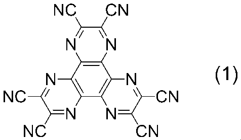

また、このように調製した電荷輸送性ワニスから得られる薄膜は、電荷輸送性、平坦性および均一性に優れることから、有機EL素子をはじめとした電子デバイス用薄膜として好適に用いることができる。特に、この薄膜を有機EL素子の正孔注入層に適用することで、低駆動電圧の有機EL素子を得ることができる。
さらに、このように調製した電荷輸送性ワニスは、スピンコート法やスリットコート法等、大面積に成膜可能な各種ウェットプロセスを用いた場合でも電荷輸送性に優れた薄膜を再現性よく製造できるため、近年の有機EL素子の分野における進展にも十分対応できる。
そして、本発明の電荷輸送性ワニスから得られる薄膜は、電荷輸送性に優れることから、有機薄膜太陽電池の陽極バッファ層、帯電防止膜等として使用されることも期待できる。
なお、本発明の電荷輸送性ワニスによって、電荷輸送性、平坦性および均一性に優れる薄膜が再現性よく得られる理由は定かではないが、比較的結晶性の低い物質を、比較的結晶性の高いジピラジノ[2,3-f:2’,3’-h]キノキサリン-2,3,6,7,10,11-ヘキサカルボニトリルとともに有機溶媒に溶解させてワニスを調製することで、当該ワニスから溶媒を除去して得られる固体膜の結晶性が低減され、その結果、ジピラジノ[2,3-f:2’,3’-h]キノキサリン-2,3,6,7,10,11-ヘキサカルボニトリルのみを溶解させたワニスによっては実現不可能であった、優れた電荷輸送性、平坦性および均一性が実現可能となったものと推測される。
本発明に係る電荷輸送性材料は、式(1)で表される化合物からなる電荷輸送性物質と、分子量200~9,000の電荷輸送性化合物(式(1)で表される化合物を除く。)(以下、単に「電荷輸送性化合物」ということがある。)とを含む。
式(1)で表される化合物は、CAS番号が105598-27-4であるジピラジノ[2,3-f:2’,3’-h]キノキサリン-2,3,6,7,10,11-ヘキサカルボニトリルである。
なお、電荷輸送性とは、導電性と同義であり、正孔輸送性とも同義である。また、本発明の電荷輸送性ワニスは、それ自体に電荷輸送性があるものでもよく、ワニスを使用して得られる固体膜に電荷輸送性があるものでもよい。

なお、薄膜化した場合に電荷輸送性物質が分離することを防ぐ観点から、電荷輸送性化合物は分子量分布のない(分散度が1)ことが好ましい(すなわち、単一の分子量であることが好ましい)。
その具体例としては、オリゴアニリン誘導体、N,N'-ジアリールベンジジン誘導体、N,N,N',N'-テトラアリールベンジジン誘導体等のアリールアミン誘導体、オリゴチオフェン誘導体、チエノチオフェン誘導体、チエノベンゾチオフェン誘導体等のチオフェン誘導体、オリゴピロール等のピロール誘導体などの各種正孔輸送性物質が挙げられるが、中でも、アリールアミン誘導体、チオフェン誘導体が好ましく、アリールアミン誘導体がより好ましく、式(2)または(3)で示されるアニリン誘導体がより一層好ましい。
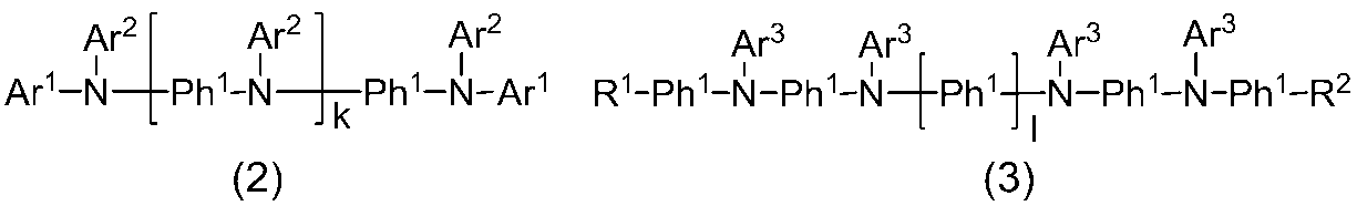
炭素数1~20のアルキル基としては、直鎖状、分岐鎖状、環状のいずれでもよく、例えば、メチル基、エチル基、n-プロピル基、イソプロピル基、n-ブチル基、イソブチル基、s-ブチル基、t-ブチル基、n-ペンチル基、n-ヘキシル基、n-ヘプチル基、n-オクチル基、n-ノニル基、n-デシル基等の炭素数1~20の直鎖または分岐鎖状アルキル基;シクロプロピル基、シクロブチル基、シクロペンチル基、シクロヘキシル基、シクロヘプチル基、シクロオクチル基、シクロノニル基、シクロデシル基、ビシクロブチル基、ビシクロペンチル基、ビシクロヘキシル基、ビシクロヘプチル基、ビシクロオクチル基、ビシクロノニル基、ビシクロデシル基等の炭素数3~20の環状アルキル基などが挙げられる。

特に、R3~R6としては、水素原子、フッ素原子、シアノ基、ハロゲン原子で置換されていてもよい炭素数1~20のアルキル基、ハロゲン原子で置換されていてもよい炭素数6~20のアリール基、ハロゲン原子で置換されていてもよい炭素数2~20のヘテロアリール基が好ましく、水素原子、フッ素原子、シアノ基、ハロゲン原子で置換されていてもよい炭素数1~10のアルキル基、ハロゲン原子で置換されていてもよいフェニル基がより好ましく、水素原子、フッ素原子、メチル基、トリフルオロメチル基がより一層好ましく、水素原子が最適である。
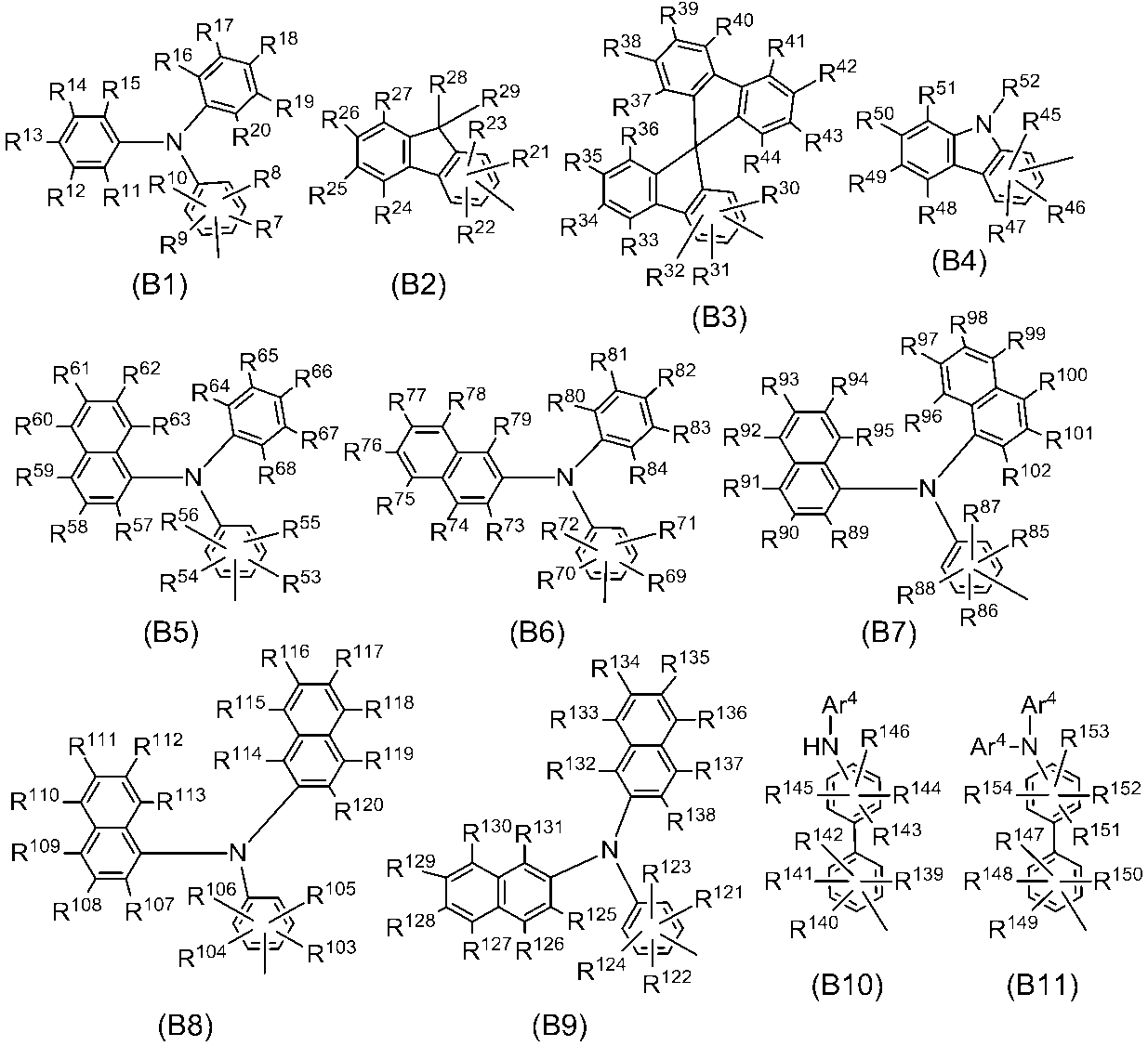
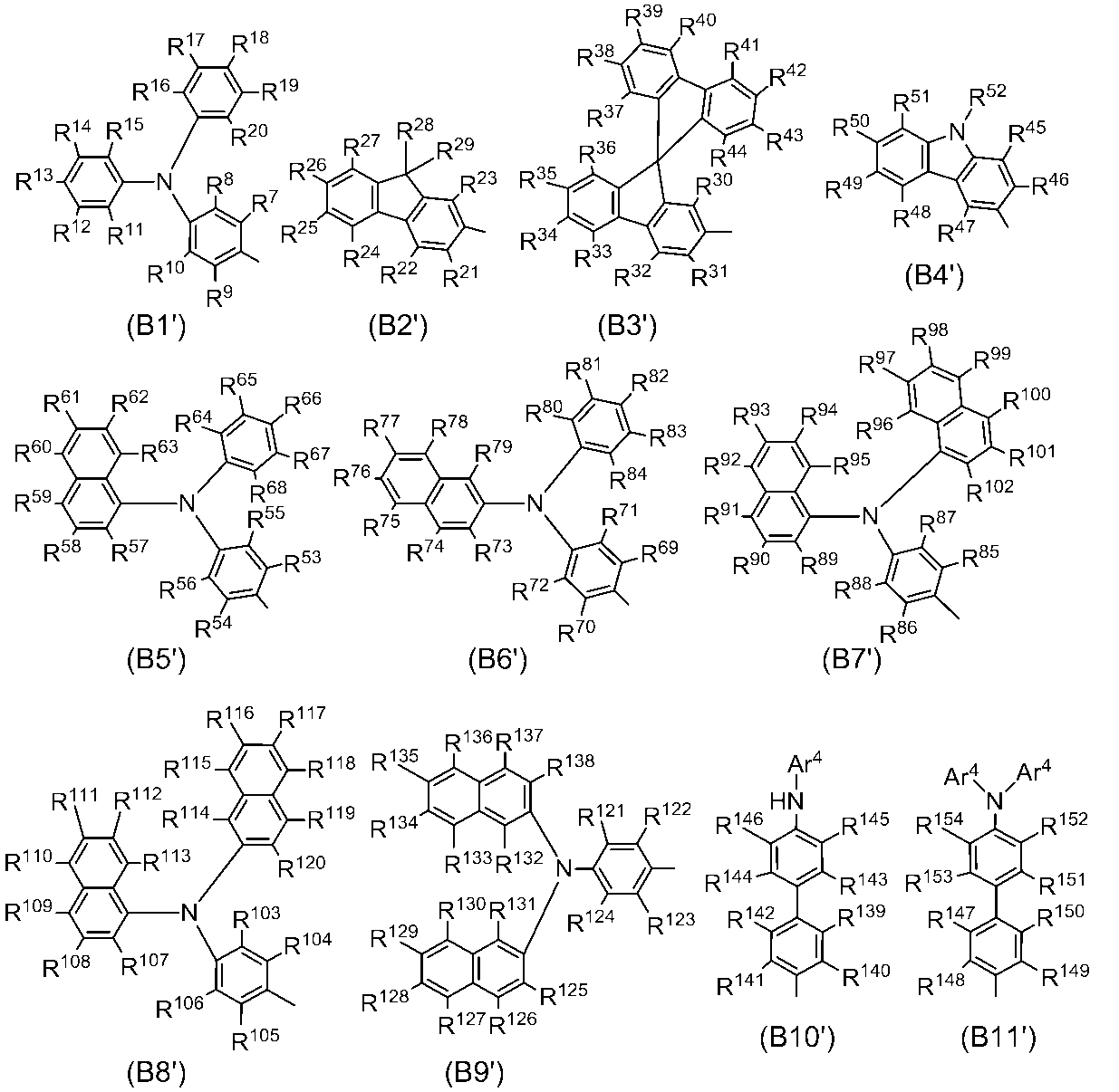
また、R28およびR29としては、Z1で置換されていてもよい炭素数6~14のアリール基、Z1で置換されていてもよい炭素数2~14のヘテロアリール基が好ましく、Z1で置換されていてもよい炭素数6~14のアリール基がより好ましく、Z1で置換されていてもよいフェニル基、Z1で置換されていてもよい1-ナフチル基、Z1で置換されていてもよい2-ナフチル基がより一層好ましい。
そして、R52としては、水素原子、Z1で置換されていてもよい炭素数6~20のアリール基、Z1で置換されていてもよい炭素数2~20のヘテロアリール基、Z4で置換されていてもよい炭素数1~20のアルキル基が好ましく、水素原子、Z1で置換されていてもよい炭素数6~14のアリール基、Z1で置換されていてもよい炭素数2~14のヘテロアリール基、Z4で置換されていてもよい炭素数1~10のアルキル基がより好ましく、水素原子、Z1で置換されていてもよい炭素数6~14のアリール基、Z1で置換されていてもよい炭素数2~14の含窒素ヘテロアリール基、Z4で置換されていてもよい炭素数1~10のアルキル基がより一層好ましく、水素原子、Z1で置換されていてもよいフェニル基、Z1で置換されていてもよい1-ナフチル基、Z1で置換されていてもよい2-ナフチル基、Z1で置換されていてもよい2-ピリジル基、Z1で置換されていてもよい3-ピリジル基、Z1で置換されていてもよい4-ピリジル基、Z4で置換されていてもよいメチル基がさらに好ましい。
炭素数6~20のアリール基の具体例としては、R1およびR2で説明したものと同様のものが挙げられ、ジ(炭素数6~20のアリール基)アミノ基の具体例としては、ジフェニルアミノ基、1-ナフチルフェニルアミノ基、ジ(1-ナフチル)アミノ基、1-ナフチル-2-ナフチルアミノ基、ジ(2-ナフチル)アミノ基等が挙げられる。
Ar4としては、フェニル基、1-ナフチル基、2-ナフチル基、1-アントリル基、2-アントリル基、9-アントリル基、1-フェナントリル基、2-フェナントリル基、3-フェナントリル基、4-フェナントリル基、9-フェナントリル基、p-(ジフェニルアミノ)フェニル基、p-(1-ナフチルフェニルアミノ)フェニル基、p-(ジ(1-ナフチル)アミノ)フェニル基、p-(1-ナフチル-2-ナフチルアミノ)フェニル基、p-(ジ(2-ナフチル)アミノ)フェニル基が好ましく、p-(ジフェニルアミノ)フェニル基がより好ましい。

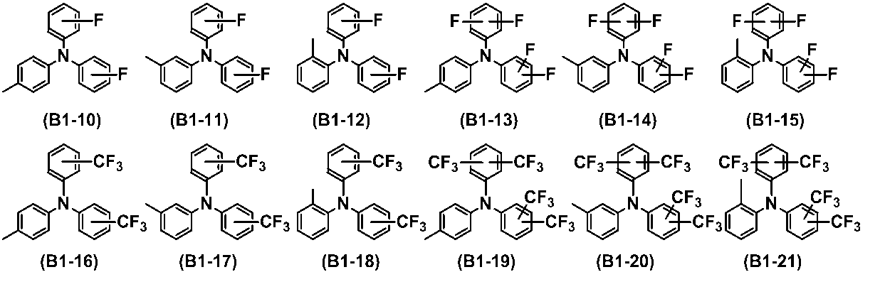


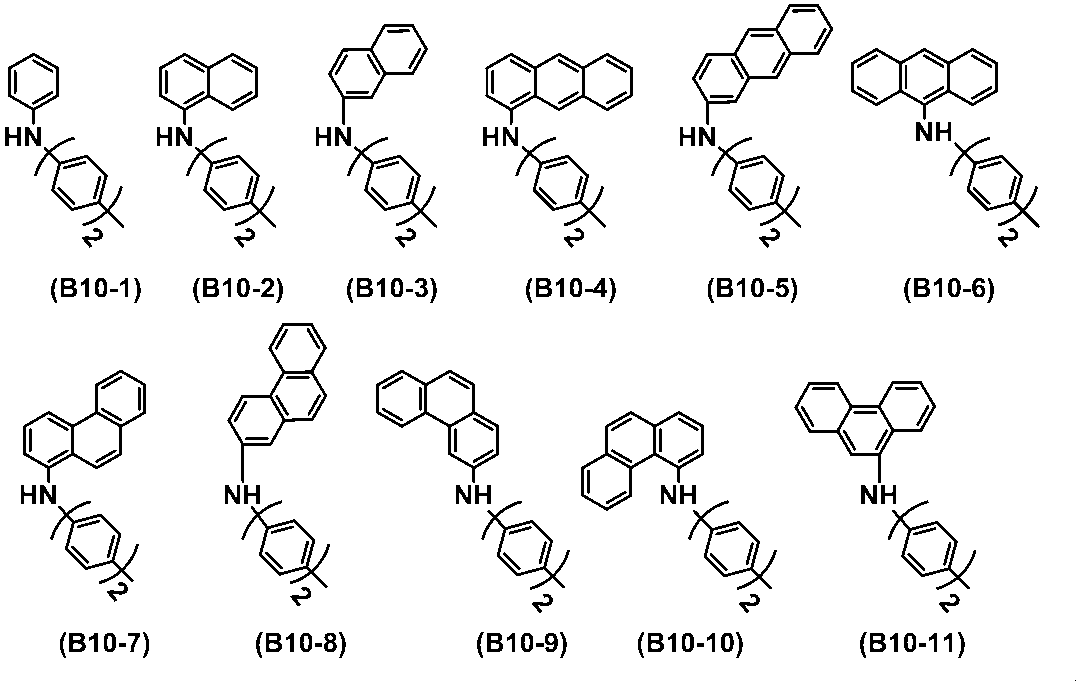
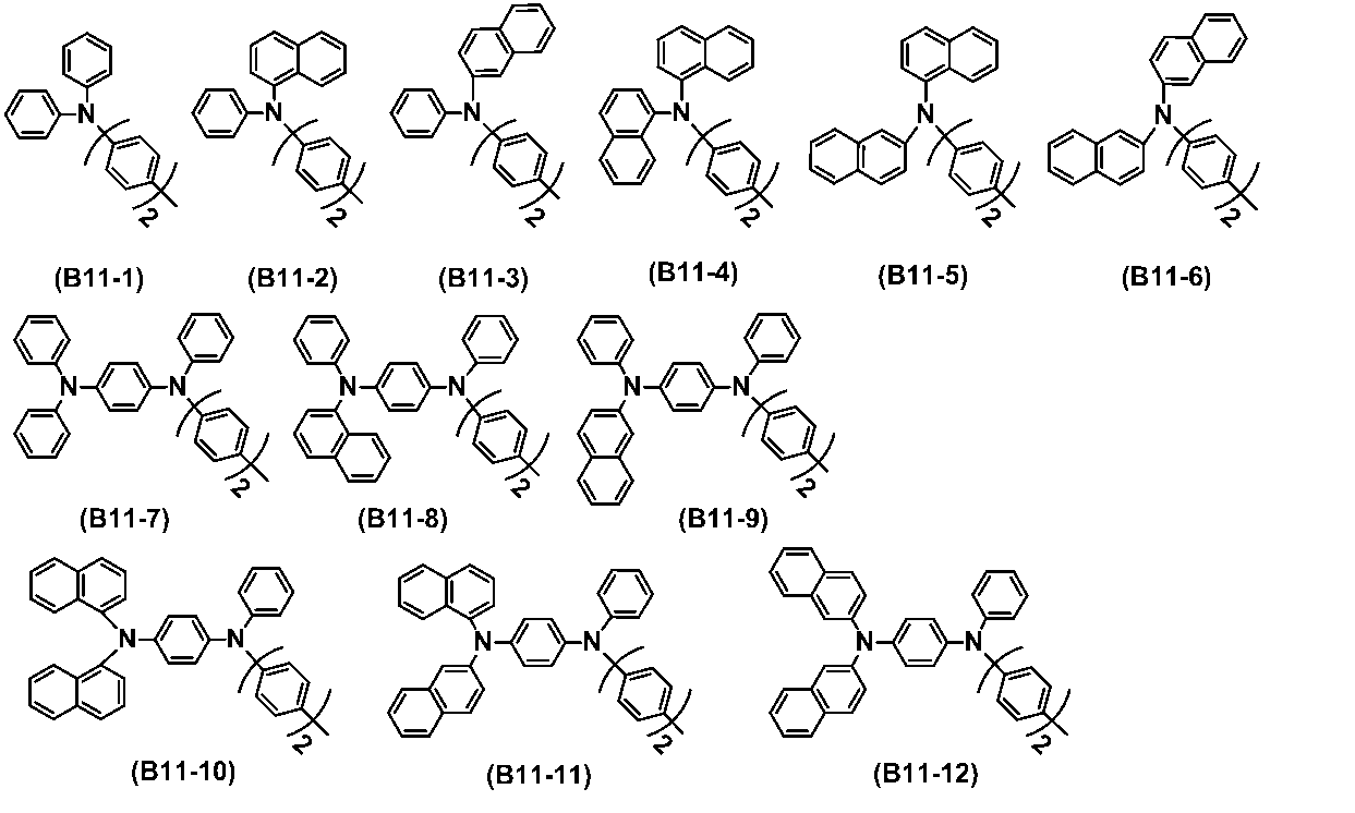


また、R156およびR157としては、Z1で置換されていてもよい炭素数6~14のアリール基、Z1で置換されていてもよい炭素数2~14のヘテロアリール基が好ましく、Z1で置換されていてもよい炭素数6~14のアリール基がより好ましく、Z1で置換されていてもよいフェニル基、Z1で置換されていてもよい1-ナフチル基、Z1で置換されていてもよい2-ナフチル基がより一層好ましい。
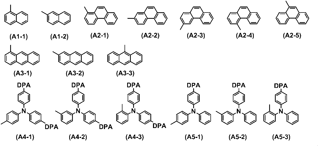
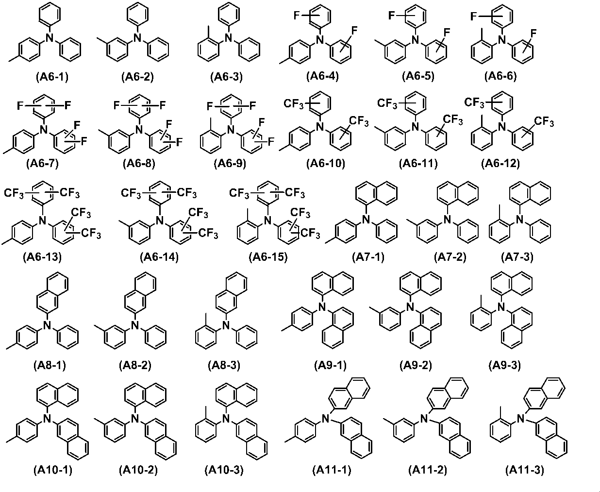
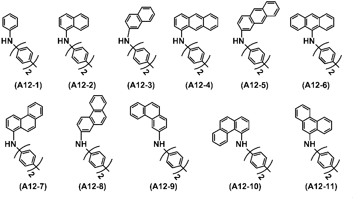
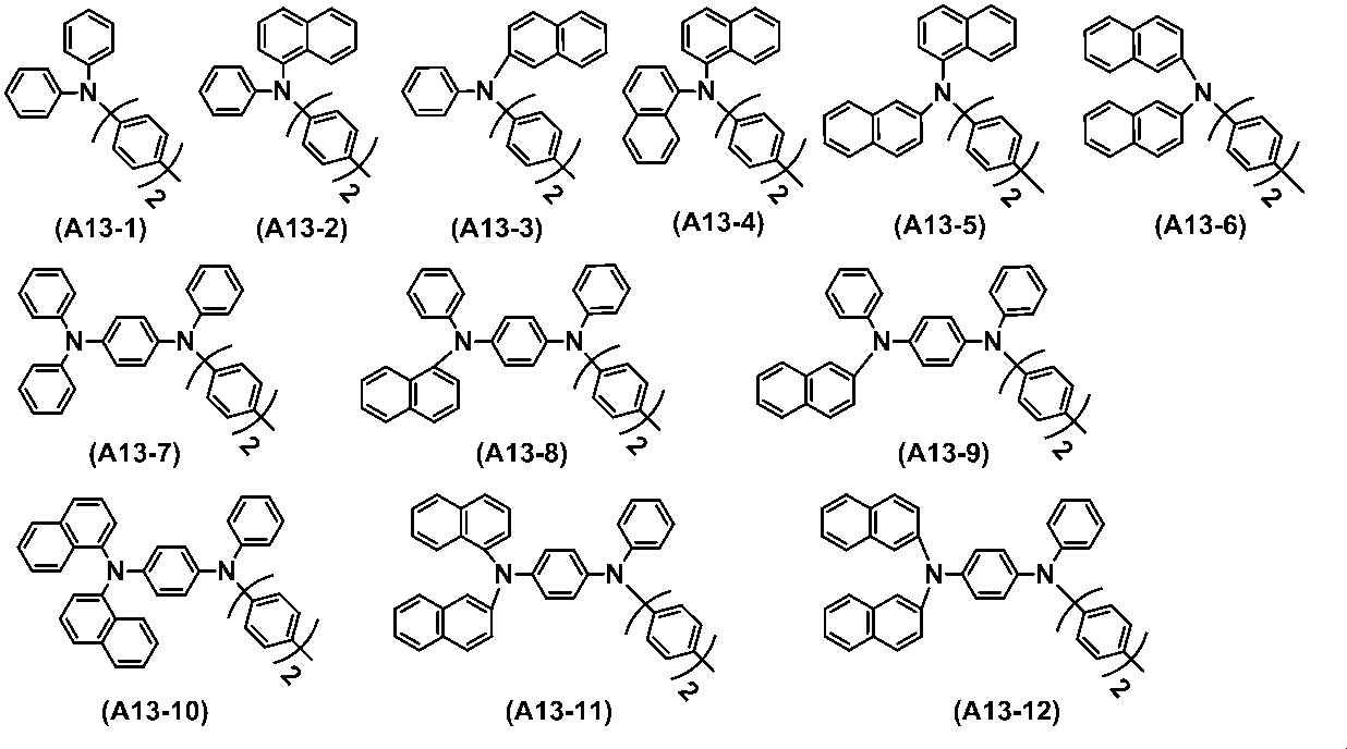

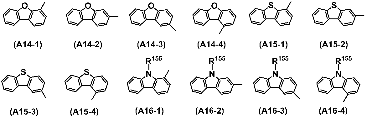
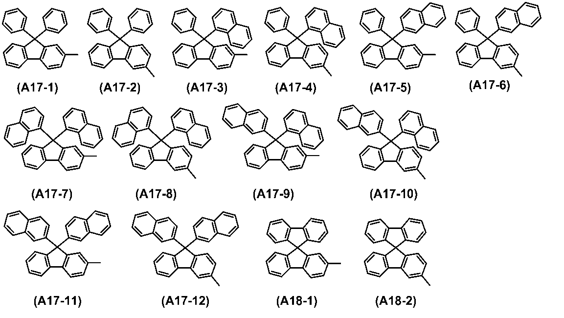
また、後述するように原料化合物として比較的安価なビス(4-アミノフェニル)アミンを用いて比較的簡便に合成できるとともに、有機溶媒に対する溶解性に優れていることからも、式(2)で表されるアニリン誘導体は、式(2-1)で表されるアニリン誘導体が好ましい。
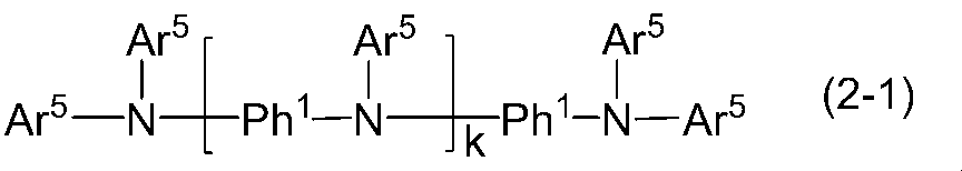
なお、Ar5の具体例としては、Ar1として好適な基の具体例として上述したものと同様のものが挙げられる。
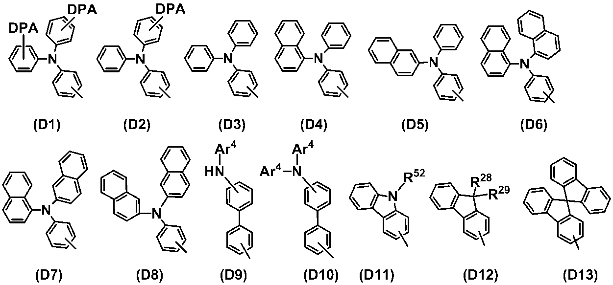

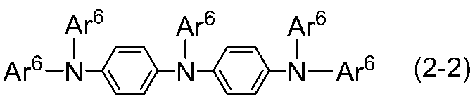
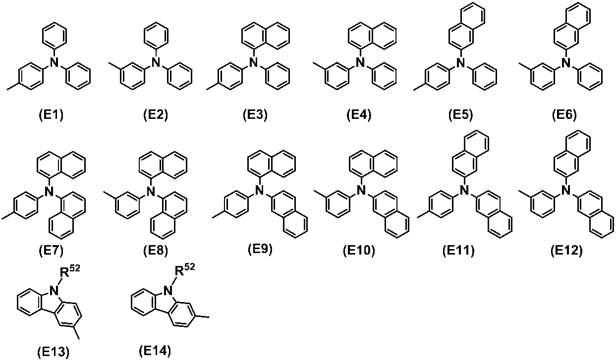

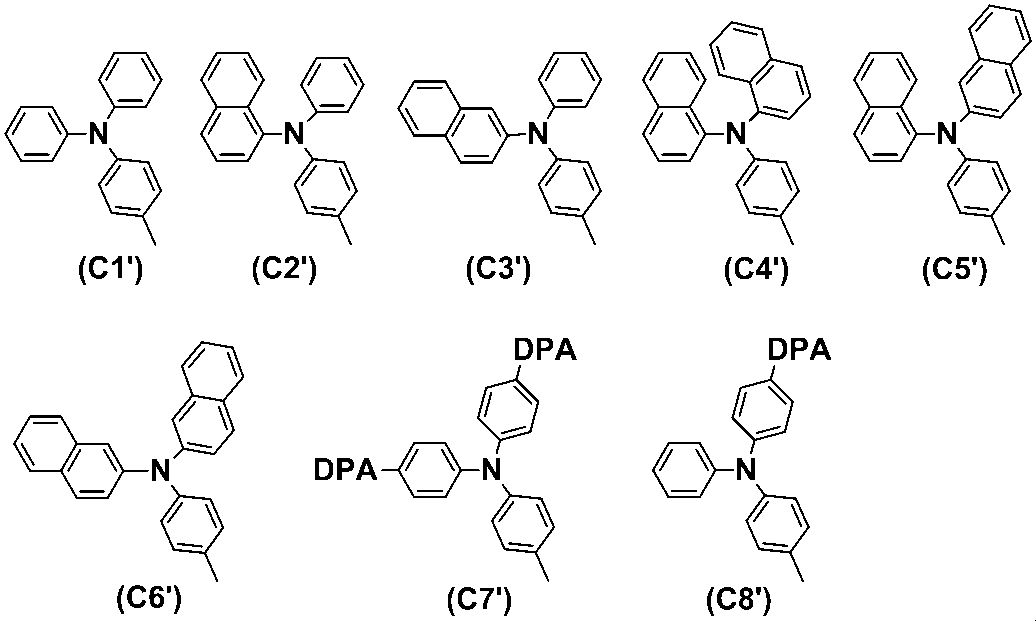
上記式(3)におけるlは、1または2を表す。
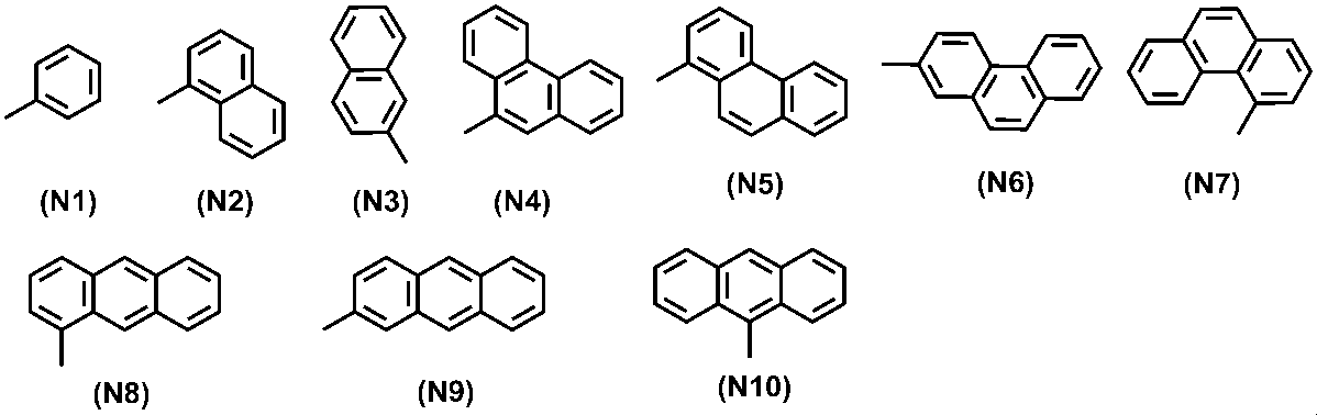


また、上記アリール基およびヘテロアリール基の炭素数は、好ましくは14以下であり、より好ましくは10以下であり、より一層好ましくは6以下である。


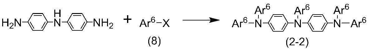
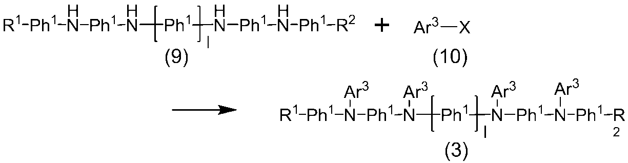
擬ハロゲン基としては、メタンスルホニルオキシ基、トリフルオロメタンスルホニルオキシ基、ノナフルオロブタンスルホニルオキシ基等の(フルオロ)アルキルスルホニルオキシ基;ベンゼンスルホニルオキシ基、トルエンスルホニルオキシ基等の芳香族スルホニルオキシ基などが挙げられる。
このような配位子としては、トリフェニルフォスフィン、トリ-o-トリルフォスフィン、ジフェニルメチルフォスフィン、フェニルジメチルフォスフィン、トリメチルフォスフィン、トリエチルフォスフィン、トリブチルフォスフィン、トリ-tert-ブチルフォスフィン、ジ-t-ブチル(フェニル)フォスフィン、ジ-tert-ブチル(4-ジメチルアミノフェニル)フォスフィン、1,2-ビス(ジフェニルフォスフィノ)エタン、1,3-ビス(ジフェニルフォスフィノ)プロパン、1,4-ビス(ジフェニルフォスフィノ)ブタン、1,1’-ビス(ジフェニルフォスフィノ)フェロセン等の3級フォスフィン、トリメチルフォスファイト、トリエチルフォスファイト、トリフェニルフォスファイト等の3級フォスファイトなどが挙げられる。
また、配位子を用いる場合、その使用量は、使用する金属錯体に対し0.1~5当量とすることができるが、1~2当量が好適である。
反応終了後は、常法にしたがって後処理をし、目的とするアニリン誘導体を得ることができる。
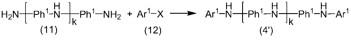
その他、当該カップリング反応における触媒、配位子、溶媒、反応温度等に関する諸条件は、式(2)で表されるアニリン誘導体の製造方法について説明した上記条件と同じである。


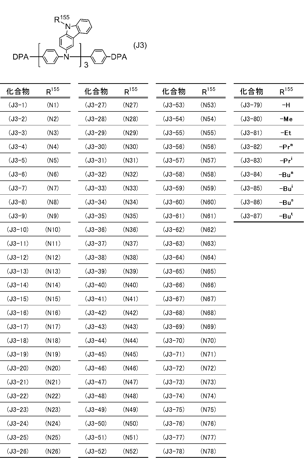


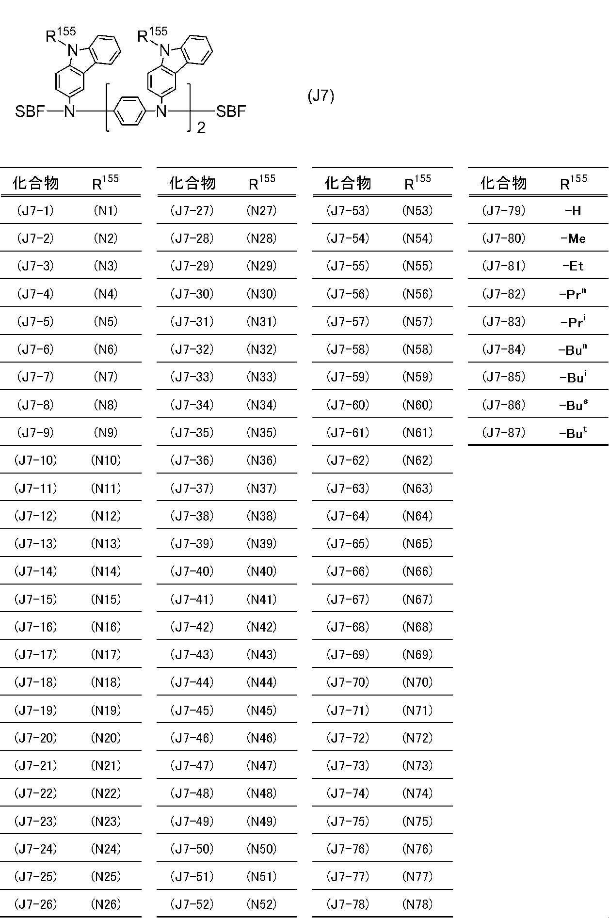


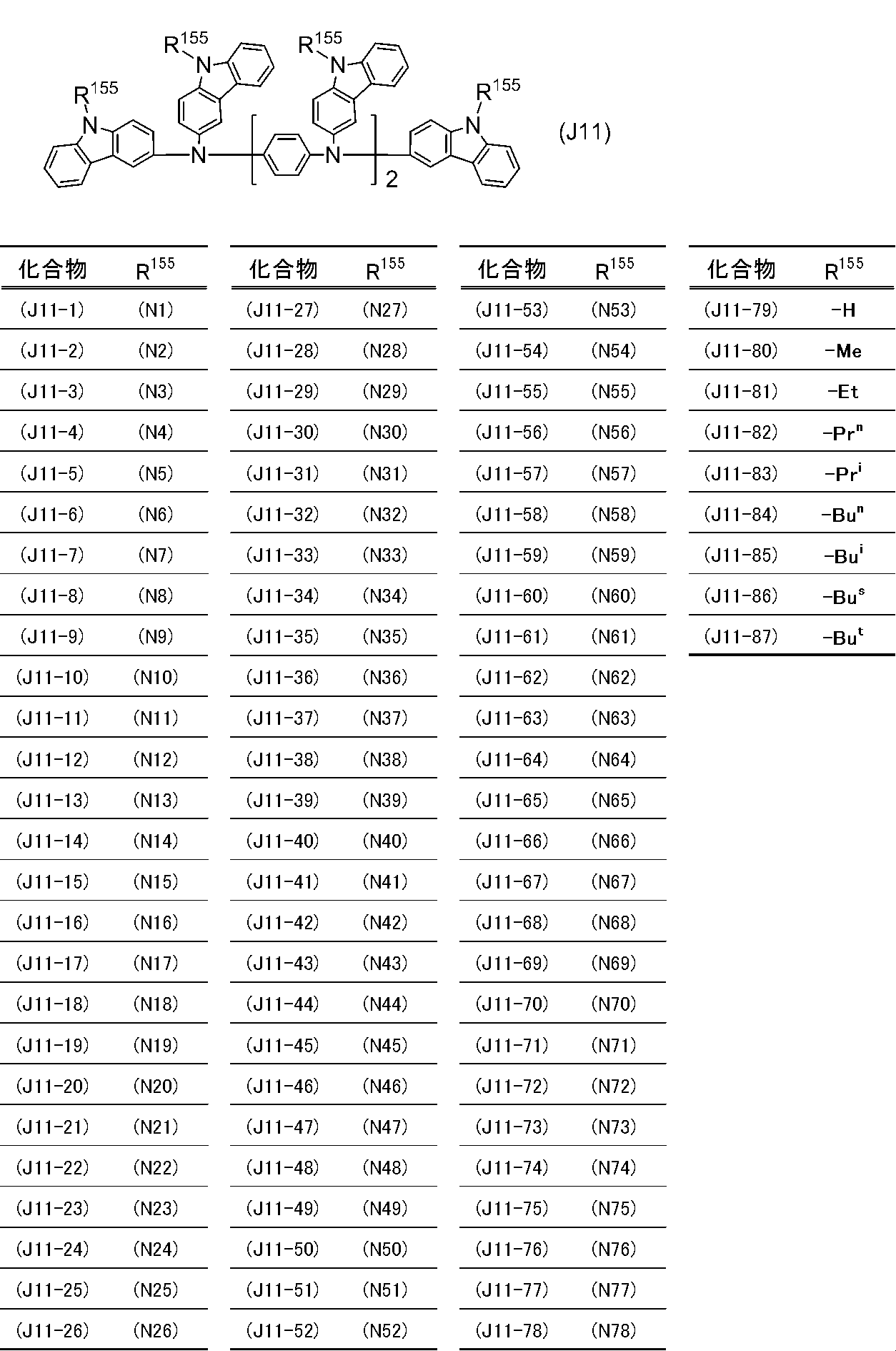


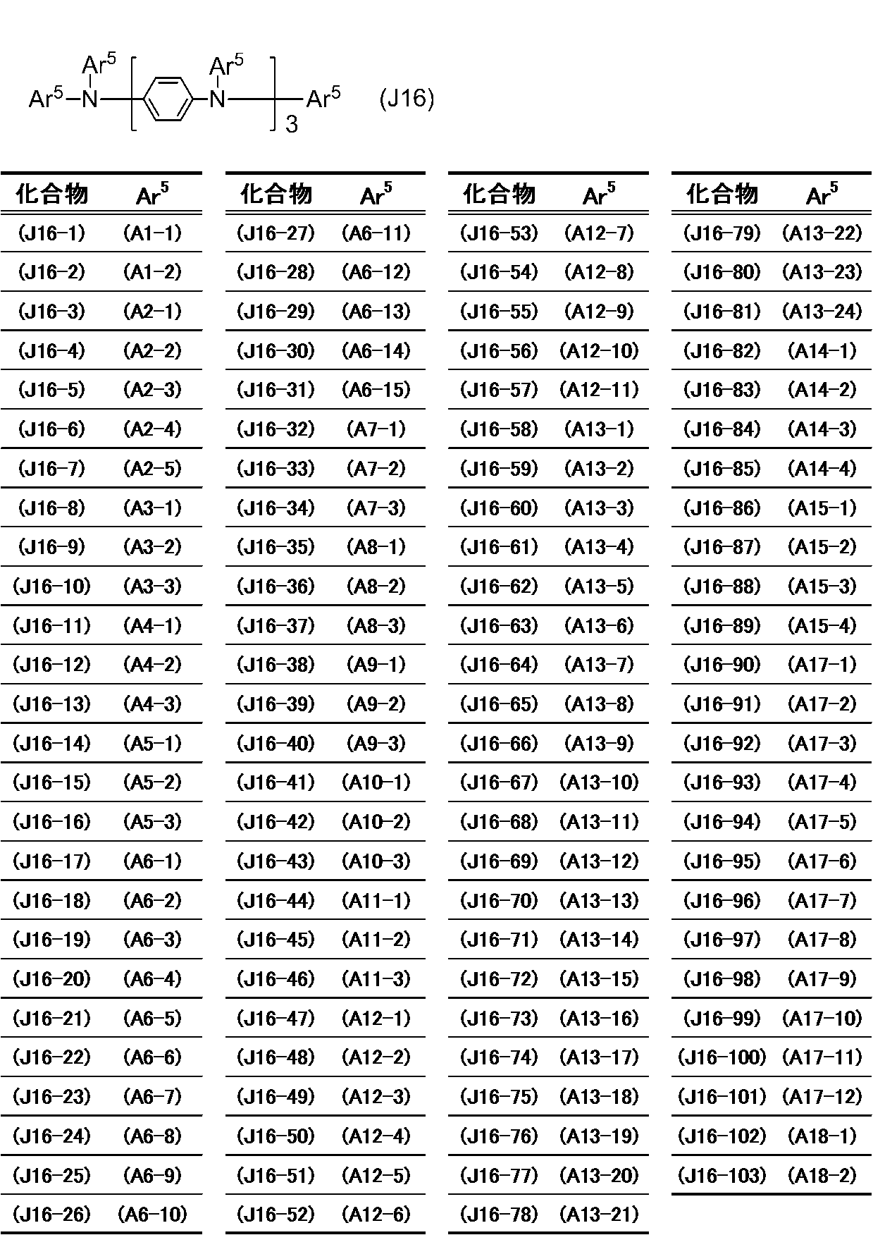
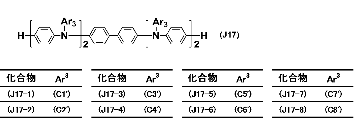
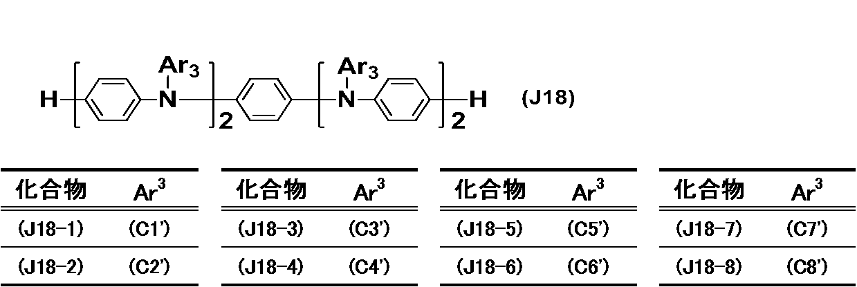
ドーパント物質としては、特に限定されるものではないが、無機系のドーパント物質、有機系のドーパント物質のいずれも使用できる。
また、無機系および有機系のドーパント物質は、1種類単独で用いてもよく、2種類以上組み合わせて用いてもよい。
ヘテロポリ酸とは、代表的に式(H1)で示されるKeggin型あるいは式(H2)で示されるDawson型の化学構造で示される、ヘテロ原子が分子の中心に位置する構造を有し、バナジウム(V)、モリブデン(Mo)、タングステン(W)等の酸素酸であるイソポリ酸と、異種元素の酸素酸とが縮合してなるポリ酸である。このような異種元素の酸素酸としては、主にケイ素(Si)、リン(P)、ヒ素(As)の酸素酸が挙げられる。

特に、1種類のヘテロポリ酸を用いる場合、その1種類のヘテロポリ酸は、リンタングステン酸またはリンモリブデン酸が好ましく、リンタングステン酸が最適である。また、2種類以上のヘテロポリ酸を用いる場合、その2種類以上のヘテロポリ酸の1つは、リンタングステン酸またはリンモリブデン酸が好ましく、リンタングステン酸がより好ましい。
なお、ヘテロポリ酸は、元素分析等の定量分析において、一般式で示される構造から元素の数が多いもの、または少ないものであっても、それが市販品として入手したもの、あるいは、公知の合成方法にしたがって適切に合成したものである限り、本発明において用いることができる。
すなわち、例えば、一般的には、リンタングステン酸は化学式H3(PW12O40)・nH2Oで、リンモリブデン酸は化学式H3(PMo12O40)・nH2Oでそれぞれ示されるが、定量分析において、この式中のP(リン)、O(酸素)またはW(タングステン)もしくはMo(モリブデン)の数が多いもの、または少ないものであっても、それが市販品として入手したもの、あるいは、公知の合成方法にしたがって適切に合成したものである限り、本発明において用いることができる。この場合、本発明に規定されるヘテロポリ酸の質量とは、合成物や市販品中における純粋なリンタングステン酸の質量(リンタングステン酸含量)ではなく、市販品として入手可能な形態および公知の合成法にて単離可能な形態において、水和水やその他の不純物等を含んだ状態での全質量を意味する。
テトラシアノキノジメタン誘導体の具体例としては、7,7,8,8-テトラシアノキノジメタン(TCNQ)や、式(H3)で表されるハロテトラシアノキノジメタンなどが挙げられる。
また、ベンゾキノン誘導体の具体例としては、テトラフルオロ-1,4-ベンゾキノン(F4BQ)、テトラクロロ-1,4-ベンゾキノン(クロラニル)、テトラブロモ-1,4-ベンゾキノン、2,3-ジクロロ-5,6-ジシアノ-1,4-ベンゾキノン(DDQ)などが挙げられる。
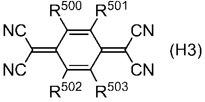
ハロゲン原子としては上記と同じものが挙げられるが、フッ素原子または塩素原子が好ましく、フッ素原子がより好ましい。
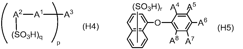
A2は、ナフタレン環またはアントラセン環を表すが、ナフタレン環が好ましい。
A3は、2~4価のパーフルオロビフェニル基を表し、pは、A1とA3との結合数を示し、2≦p≦4を満たす整数であるが、A3がパーフルオロビフェニルジイル基、好ましくはパーフルオロビフェニル-4,4’-ジイル基であり、かつ、pが2であることが好ましい。
qは、A2に結合するスルホン酸基数を表し、1≦q≦4を満たす整数であるが、2が最適である。
その他、ハロゲン原子、炭素数1~20のアルキル基の例としては上記と同様のものが挙げられるが、ハロゲン原子としては、フッ素原子が好ましい。
なお、パーフルオロアルキル基とは、アルキル基の水素原子全てがフッ素原子に置換された基であり、パーフルオロアルケニル基とは、アルケニル基の水素原子全てがフッ素原子に置換された基である。
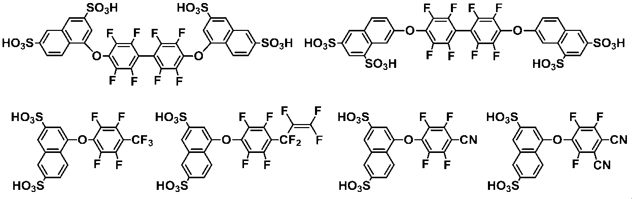
アリールスルホン酸化合物は市販品を用いてもよいが、国際公開第2006/025342号、国際公開第2009/096352号等に記載の公知の方法で合成することもできる。
このような高溶解性溶媒としては、例えば、シクロヘキサノン、N,N-ジメチルホルムアミド、N,N-ジメチルアセトアミド、N-メチルピロリドン、1,3-ジメチル-2-イミダゾリジノン、ジエチレングリコールモノメチルエーテル等の有機溶媒が挙げられるが、これらに限定されるものではない。これらの溶媒は1種単独で、または2種以上混合して用いることができ、その使用量は、ワニスに使用する溶媒全体に対して5~100質量%とすることができる。
高粘度有機溶媒としては、例えば、シクロヘキサノール、エチレングリコール、エチレングリコールジグリシジルエーテル、1,3-オクチレングリコール、ジエチレングリコール、ジプロピレングリコール、トリエチレングリコール、トリプロピレングリコール、1,3-ブタンジオール、2,3-ブタンジオール、1,4-ブタンジオール、プロピレングリコール、へキシレングリコール等が挙げられるが、これらに限定されるものではない。これらの溶媒は単独で用いてもよく、2種以上混合して用いてもよい。
本発明のワニスに用いられる溶媒全体に対する高粘度有機溶媒の添加割合は、固体が析出しない範囲内であることが好ましく、固体が析出しない限りにおいて、添加割合は、5~90質量%が好ましい。
このような溶媒としては、例えば、プロピレングリコールモノメチルエーテル、エチレングリコールモノブチルエーテル、ジエチレングリコールジエチルエーテル、ジエチレングリコールジメチルエーテル、ジエチレングリコールモノエチルエーテルアセテート、ジエチレングリコールモノブチルエーテルアセテート、ジプロピレングリコールモノメチルエーテル、プロピレングリコールモノメチルエーテルアセテート、ジエチレングリコールモノエチルエーテル、ジアセトンアルコール、γ-ブチロラクトン、エチルラクテート、n-ヘキシルアセテート等が挙げられるが、これらに限定されるものではない。これらの溶媒は1種単独で、または2種以上混合して用いることができる。
この有機シラン化合物としては、ジアルコキシシラン化合物、トリアルコキシシラン化合物またはテトラアルコキシシラン化合物が挙げられ、これらは単独で用いてもよく、2種以上組み合わせて用いてもよい。
本発明においては、有機シラン化合物は、ジアルコキシシラン化合物およびトリアルコキシシラン化合物から選ばれる1種を含むことが好ましく、トリアルコキシシラン化合物を含むことがより好ましく、フッ素原子含有トリアルコキシシラン化合物を含むことがより一層好ましい。
Si(OR)4 (S1)
SiR′(OR)3 (S2)
Si(R′)2(OR)2 (S3)
Z10は、ハロゲン原子、アミノ基、ニトロ基、シアノ基またはチオール基を表す。
RおよびR′において、アルキル基、アルケニル基およびアルキニル基の炭素数は、好ましくは10以下であり、より好ましくは6以下であり、より一層好ましくは4以下である。
また、アリール基およびヘテロアリール基の炭素数は、好ましくは14以下であり、より好ましくは10以下であり、より一層好ましくは6以下である。
R′としては、Z8で置換されていてもよい炭素数1~20のアルキル基またはZ9で置換されていてもよい炭素数6~20のアリール基が好ましく、Z8で置換されていてもよい炭素数1~10のアルキル基またはZ9で置換されていてもよい炭素数6~14のアリール基がより好ましく、Z8で置換されていてもよい炭素数1~6のアルキル基、またはZ9で置換されていてもよい炭素数6~10のアリール基がより一層好ましく、Z8で置換されていてもよい炭素数1~4のアルキル基またはZ9で置換されていてもよいフェニル基がさらに好ましい。
なお、複数のRは、すべて同一でも異なっていてもよく、複数のR′も、すべて同一でも異なっていてもよい。
Z7としては、ハロゲン原子またはZ10で置換されていてもよい炭素数6~20のアルキル基が好ましく、フッ素原子またはZ10で置換されていてもよい炭素数1~10のアルキル基がより好ましく、存在しないこと(すなわち、非置換であること)が最適である。
Z9としては、ハロゲン原子、Z10で置換されていてもよい炭素数1~20のアルキル基、Z10で置換されていてもよいフラニル基、エポキシシクロヘキシル基、グリシドキシ基、メタクリロキシ基、アクリロキシ基、ウレイド基、チオール基、イソシアネート基、アミノ基、Z10で置換されていてもよいフェニルアミノ基、またはZ10で置換されていてもよいジフェニルアミノ基が好ましく、ハロゲン原子がより好ましく、フッ素原子、または存在しないこと(すなわち、非置換であること)がより一層好ましい。
Z10としては、ハロゲン原子が好ましく、フッ素原子または存在しないこと(すなわち、非置換であること)がより好ましい。
ジアルコキシシラン化合物の具体例としては、ジメチルジメトキシシラン、ジメチルジエトキシシラン、メチルエチルジメトキシシラン、ジエチルジメトキシシラン、ジエチルジエトキシシラン、メチルプロピルジメトキシシラン、メチルプロピルジエトキシシラン、ジイソプロピルジメトキシシラン、フェニルメチルジメトキシシラン、ビニルメチルジメトキシシラン、3-グリシドキシプロピルメチルジメトキシシシラン、3-グリシドキシプロピルメチルジエトキシシシラン、3-(3,4-エポキシシクロヘキシル)エチルメチルジメトキシシラン、3-メタクリロキシプロピルメチルジメトキシシラン、3-メタクリロキシプロピルメチルジエトキシシラン、3-メルカプトプロピルメチルジメトキシシラン、γ-アミノプロピルメチルジエトキシシラン、N-(2-アミノエチル)アミノプロピルメチルジメトキシシラン、3,3,3-トリフルオロプロピルメチルジメトキシシラン等が挙げられる。
このような重合体の好ましい一例としては、予めアルコキシシラン化合物を加水分解縮合して調製された重量平均分子量500~10,000の重合体からなる有機シラン化合物であって、アルコキシシラン化合物が、式(S4)および(S5)で表されるアルコキシシラン化合物から選ばれる少なくとも1種を含むものが挙げられる。
とりわけ、重合体の分子量をより高める観点から、式(S4)で表されるトリアルコキシシラン化合物が含まれることが好ましい。
SiR′′(OR′′′)3 (S4)
Si(R′′)2(OR′′′)2 (S5)
また、アリール基およびヘテロアリール基の炭素数は、好ましくは14以下であり、より好ましくは10以下であり、より一層好ましくは6以下である。
Z11およびZ12としては、ハロゲン原子が好ましく、フッ素原子が最適であり、Z13としては、R′′′においては存在しない(すなわち、非置換である)ことが好ましく、Z11およびZ12においてはハロゲン原子が好ましく、フッ素原子が最適である。
Z12で置換された炭素数6~20のアリール基としては、上記Z13で置換された炭素数6~20のアリール基で例示した基に加え、4-トリクロロメチルフェニル基、4-トリブロモメチルフェニル基、4-トリフルオロメチルフェニル基等のハロゲン化アルキル基を有するアリール基等が挙げられるが、フッ化アルキル基を有するアリール基が好ましい。
Si(OR′′′′)4 (S6)
Si(R′′′′′)2(OR′′′′)2 (S7)
SiR′′′′′(OR′′′′)3 (S8)
また、アリール基およびヘテロアリール基の炭素数は、好ましくは14以下であり、より好ましくは10以下であり、より一層好ましくは6以下である。
R′′′′′としては、炭素数1~20のアルキル基または炭素数6~20のアリール基が好ましく、炭素数1~10のアルキル基または炭素数6~14のアリール基がより好ましく、炭素数1~6のアルキル基または炭素数6~10のアリール基がより一層好ましく、炭素数1~4のアルキル基またはフェニル基がさらに好ましい。
なお、複数のR′′′′は、すべて同一でも異なっていてもよく、複数のR′′′′′も、すべて同一でも異なっていてもよい。
Z14としては、ハロゲン原子、Z16で置換されていてもよいフェニル基、Z16で置換されていてもよいフラニル基が好ましく、ハロゲン原子がより好ましく、フッ素原子、または存在しないこと(すなわち、非置換であること)がより一層好ましい。
Z15としては、ハロゲン原子、Z16で置換されていてもよい炭素数1~20のアルキル基、Z16で置換されていてもよいフラニル基が好ましく、ハロゲン原子がより好ましく、フッ素原子、または存在しないこと(すなわち、非置換であること)がより一層好ましい。
Z16としては、ハロゲン原子が好ましく、フッ素原子または存在しないこと(すなわち、非置換であること)がより好ましい。
上記式(S7)で表されるジアルコキシシラン化合物の具体例としては、ジメチルジメトキシシラン、ジメチルジエトキシシラン、メチルエチルジメトキシシラン、ジエチルジメトキシシラン、ジエチルジエトキシシラン、メチルプロピルジメトキシシラン、メチルプロピルジエトキシシラン、ジイソプロピルジメトキシシラン、フェニルメチルジメトキシシラン、ビニルメチルジメトキシシラン等が挙げられる。
上記式(S8)で表されるトリアルコキシシラン化合物の具体例としては、メチルトリメトキシシラン、メチルトリエトキシシラン、エチルトリメトキシシラン、エチルトリエトキシシラン、プロピルトリメトキシシラン、プロピルトリエトキシシラン、ブチルトリメトキシシラン、ブチルトリエトキシシラン、ペンチルトリメトキシシラン、ペンチルトリエトキシシラン、ヘプチルトリメトキシシラン、ヘプチルトリエトキシシラン、オクチルトリメトキシシラン、オクチルトリエトキシシラン、ドデシルトリメトキシシラン、ドデシルトリエトキシシラン、ヘキサデシルトリメトキシシラン、ヘキサデシルトリエトキシシラン、オクタデシルトリメトキシシラン、オクタデシルトリエトキシシラン、フェニルトリメトキシシラン、フェニルトリエトキシシラン、ビニルトリメトキシシラン、ビニルトリエトキシシラン、トリエトキシ-2-チエニルシラン、3-(トリエトキシシリル)フラン等が挙げられる。
加水分解の手法としては、特に限定されるものではなく一般的な手法を用いればよい。一例を挙げると、アルコキシシラン化合物を、水系溶媒中で20~100℃程度で1~24時間処理する手法が挙げられる。この際、酸または塩基を触媒として用いることもできる。
また、電荷輸送性ワニスの固形分濃度は、ワニスの粘度および表面張力等や、作製する薄膜の厚み等を勘案して適宜設定されるものではあるが、通常、0.1~10.0質量%程度であり、ワニスの塗布性を向上させることを考慮すると、好ましくは0.5~5.0質量%程度、より好ましくは1.0~3.0質量%程度である。
また、有機溶媒が複数ある場合は、例えば、式(1)で表される化合物と電荷輸送性化合物をよく溶解する溶媒に、まずこれらを溶解させ、そこへその他の溶媒を加えてもよく、複数の有機溶媒の混合溶媒に、式(1)で表される化合物、電荷輸送性化合物を順次、あるいはこれらを同時に溶解させてもよい。
ワニスの塗布方法としては、特に限定されるものではなく、ディップ法、スピンコート法、転写印刷法、ロールコート法、刷毛塗り、インクジェット法、スプレー法、スリットコート法等が挙げられ、塗布方法に応じてワニスの粘度および表面張力を調節することが好ましい。
なお、焼成の際、より高い均一成膜性を発現させたり、基材上で反応を進行させたりする目的で、2段階以上の温度変化をつけてもよく、加熱は、例えば、ホットプレートやオーブン等、適当な機器を用いて行えばよい。
有機EL素子の代表的な構成としては、以下(a)~(f)が挙げられるが、これらに限定されるわけではない。なお、下記構成において、必要に応じて、発光層と陽極の間に電子ブロック層等を、発光層と陰極の間にホール(正孔)ブロック層等を設けることもできる。また、正孔注入層、正孔輸送層あるいは正孔注入輸送層が電子ブロック層等としての機能を兼ね備えていてもよく、電子注入層、電子輸送層あるいは電子注入輸送層がホール(正孔)ブロック層等としての機能を兼ね備えていてもよい。
(a)陽極/正孔注入層/正孔輸送層/発光層/電子輸送層/電子注入層/陰極
(b)陽極/正孔注入層/正孔輸送層/発光層/電子注入輸送層/陰極
(c)陽極/正孔注入輸送層/発光層/電子輸送層/電子注入層/陰極
(d)陽極/正孔注入輸送層/発光層/電子注入輸送層/陰極
(e)陽極/正孔注入層/正孔輸送層/発光層/陰極
(f)陽極/正孔注入輸送層/発光層/陰極
「電子注入層」、「電子輸送層」および「電子注入輸送層」とは、発光層と陰極との間に形成される層であって、電子を陰極から発光層へ輸送する機能を有するものであり、発光層と陰極の間に、電子輸送性材料の層が1層のみ設けられる場合、それが「電子注入輸送層」であり、発光層と陰極の間に、電子輸送性材料の層が2層以上設けられる場合、陰極に近い層が「電子注入層」であり、それ以外の層が「電子輸送層」である。
「発光層」とは、発光機能を有する有機層であって、ドーピングシステムを採用する場合、ホスト材料とドーパント材料を含んでいる。このとき、ホスト材料は、主に電子と正孔の再結合を促し、励起子を発光層内に閉じ込める機能を有し、ドーパント材料は、再結合で得られた励起子を効率的に発光させる機能を有する。燐光素子の場合、ホスト材料は主にドーパントで生成された励起子を発光層内に閉じ込める機能を有する。
使用する電極基板は、洗剤、アルコール、純水等による液体洗浄を予め行って浄化しておくことが好ましく、例えば、陽極基板では使用直前にUVオゾン処理、酸素-プラズマ処理等の表面処理を行うことが好ましい。ただし陽極材料が有機物を主成分とする場合、表面処理を行わなくともよい。
上記の方法により、陽極基板上に本発明の電荷輸送性ワニスを塗布して焼成し、電極上に正孔注入層を作製する。
この正孔注入層の上に、正孔輸送層、発光層、電子輸送層、電子注入層、陰極をこの順で設ける。正孔輸送層、発光層、電子輸送層および電子注入層は、用いる材料の特性等に応じて、蒸着法、塗布法(ウェットプロセス)のいずれかで形成すればよい。
陽極材料としては、インジウム錫酸化物(ITO)、インジウム亜鉛酸化物(IZO)に代表される透明電極や、アルミニウムに代表される金属やこれらの合金等から構成される金属陽極が挙げられ、平坦化処理を行ったものが好ましい。高電荷輸送性を有するポリチオフェン誘導体やポリアニリン誘導体を用いることもできる。
なお、金属陽極を構成するその他の金属としては、スカンジウム、チタン、バナジウム、クロム、マンガン、鉄、コバルト、ニッケル、銅、亜鉛、ガリウム、イットリウム、ジルコニウム、ニオブ、モリブデン、ルテニウム、ロジウム、パラジウム、カドミウム、インジウム、スカンジウム、ランタン、セリウム、プラセオジム、ネオジム、プロメチウム、サマリウム、ユウロピウム、ガドリニウム、テルビウム、ジスプロシウム、ホルミウム、エルビウム、ツリウム、イッテルビウム、ハフニウム、タリウム、タングステン、レニウム、オスミウム、イリジウム、プラチナ、金、チタン、鉛、ビスマスやこれらの合金等が挙げられるが、これらに限定されるわけではない。
陰極材料としては、アルミニウム、マグネシウム-銀合金、アルミニウム-リチウム合金、リチウム、ナトリウム、カリウム、セシウム等が挙げられる。
上記EL素子作製において、正孔輸送層、発光層、電子輸送層、電子注入層の真空蒸着操作を行う代わりに、正孔輸送層(以下、正孔輸送性高分子層)、発光層(以下、発光性高分子層)を順次形成することによって本発明の電荷輸送性ワニスによって形成される電荷輸送性薄膜を有する有機EL素子を作製することができる。
具体的には、陽極基板上に本発明の電荷輸送性ワニスを塗布して上記の方法により正孔注入層を作製し、その上に正孔輸送性高分子層、発光性高分子層を順次形成し、さらに陰極電極を蒸着して有機EL素子とする。
正孔輸送性高分子層および発光性高分子層の形成法としては、正孔輸送性高分子材料もしくは発光性高分子材料、またはこれらにドーパント物質を加えた材料に溶媒を加えて溶解するか、均一に分散し、正孔注入層または正孔輸送性高分子層の上に塗布した後、それぞれ焼成することで成膜する方法が挙げられる。
塗布方法としては、特に限定されるものではなく、インクジェット法、スプレー法、ディップ法、スピンコート法、転写印刷法、ロールコート法、刷毛塗り等が挙げられる。なお、塗布は、窒素、アルゴン等の不活性ガス下で行うことが好ましい。
焼成する方法としては、不活性ガス下または真空中、オーブンまたはホットプレートで加熱する方法が挙げられる。
陽極基板上に正孔注入層を形成する。その層の上に、上記の方法により本発明の電荷輸送性ワニスを塗布して焼成し、正孔輸送層を作製する。
この正孔輸送層の上に、発光層、電子輸送層、電子注入層、陰極をこの順で設ける。発光層、電子輸送層および電子注入層の形成方法および具体例は上述と同様のものが挙げられる。また、正孔注入層は、用いる材料の特性等に応じて、蒸着法、塗布法(ウェットプロセス)のいずれかで形成すればよい。
陽極基板上に正孔注入輸送層を形成し、この正孔注入輸送層の上に、発光層、電子輸送層、電子注入層、陰極をこの順で設ける。発光層、電子輸送層および電子注入層の形成方法および具体例は上述と同様のものが挙げられる。
通常、ボトムエミッション構造の素子では、基板側に透明陽極が用いられ、基板側から光が取り出されるのに対し、トップエミッション構造の素子では、金属からなる反射陽極が用いられ、基板と反対方向にある透明電極(陰極)側から光が取り出されることから、例えば陽極材料について言えば、ボトムエミッション構造の素子を製造する際はITO等の透明陽極を、トップエミッション構造の素子を製造する際はAl/Nd等の反射陽極を、それぞれ用いる。
(1)分子量測定:昭和電工(株)製、常温ゲル浸透クロマトグラフィー(GPC)装置(GPC-101)およびShodex製カラム(KD-803L)
(測定条件)
・カラム温度:40℃
・溶離液:テトラヒドロフラン(THF),10ml/L
・流速:1.0ml/分
・検量線作成用標準サンプル:昭和電工(株)製、SL-105,標準ポリスチレン(分子量約580,2970,7200,19900,52400)
(2)基板洗浄:長州産業(株)製 基板洗浄装置(減圧プラズマ方式)
(3)ワニスの塗布:ミカサ(株)製 スピンコーターMS-A100
(4)膜厚測定:(株)小坂研究所製 微細形状測定機サーフコーダET-4000
(5)膜の表面観察:レーザーテック社製 共焦点レーザー顕微鏡 リアルタイム走査型レーザー顕微鏡 1LM21D
(6)EL素子の作製:長州産業(株)製 多機能蒸着装置システムC-E2L1G1-N
(7)EL素子の輝度等の測定:(有)テック・ワールド製 I-V-L測定システム
(8)EL素子の寿命測定(輝度半減期測定):(株)イーエッチシー製 有機EL輝度寿命評価システムPEL-105S
[合成例1]
式(TP1)で表されるチオフェン誘導体(以下「TP1」という。)を以下の方法により合成した
その後、再び-78℃に冷却して30分間撹拌した後、トリブチルクロロスタナン8.8mLを滴下して10分撹拌し、次いで0℃に昇温してさらに30分間撹拌した。
撹拌後、反応混合物から減圧下で溶媒を留去し、得られた残渣をトルエンに加え、ろ過によって不溶物を除去し、得られたろ液から減圧下で溶媒を留去し、ターチオフェンのビススタニル体を含むオイル状物12.88g(当該ビススタニル体の純度51.91%)得た。
次いで、窒素雰囲気下で、別のフラスコ内に、このターチオフェンビススタニル体を含むオイル状物6.44g、2-ブロモ-3-ノルマルヘキシルチオフェン2.41g、トルエン24mLおよびテトラキス(トリフェニルホスフィン)パラジウム0.23gを順次入れて、還流条件下4.5時間撹拌した。
室温まで放冷し、溶媒を減圧留去した後、ろ過にて不溶物を除去した。得られたろ液を濃縮し、シリカゲルカラムクロマトグラフィーにて精製し、TP1を得た(収量:1.29g、収率:55%、2段階通算収率)。
1H-NMR(CDCl3):7.17(d,J=5.1Hz,2H),7.12(d,J=3.9Hz,2H),7.09(s,2H),7.01(d,J=3.9Hz,2H),6.93(d,J=5.1Hz,2H),2.78(t,J=7.7Hz,4H),1.54-1.70(m,4H),1.28-1.41(m,12H),0.89(t,J=7.0Hz,6H).

撹拌終了後、反応混合物を室温まで冷却し、冷却した反応混合物と、トルエンと、イオン交換水とを混合して分液処理をした。得られた有機層を硫酸ナトリウムで乾燥し、濃縮した。濃縮液をシリカゲルにてろ過を行い、得られたろ液に活性炭0.2gを加え、室温で30分撹拌した。
その後、ろ過にて活性炭を取り除き、ろ液を濃縮した。濃縮液をメタノールおよび酢酸エチルの混合溶媒(500mL/500mL)に滴下し、得られたスラリーを室温で一晩撹拌し、次いでスラリーをろ過してろ物を回収した。得られたろ物を乾燥し、目的とするアニリン誘導体(PCZ5)を得た(収量5.88g,収率83%)。
1H-NMR(300MHz,THF-d8)δ[ppm]:8.08(d,J=7.7Hz,2H),7.99(d,J=7.7Hz,8H),7.60-7.64(m,19H),7.42-7.47(m,6H),7.28-7.36(m,19H),7.09-7.21(m,6H),7.00(m,8H).
MALDI-TOF-MS m/Z found:1404.68([M]+calcd:1404.56).
温度計および還流管を備え付けた200mLの四つ口反応フラスコ中で、ヘキシレングリコール18.4g、ブチルセロソルブS6.1g、テトラエトキシシラン23.3g、および3,3,3-トリフルオロプロピルトリメトキシシラン10.5gを混合し、アルコキシシランモノマーの溶液を調製した。
この溶液に、予めヘキシレングリコール9.2g、ブチルセロソルブ3.1g、水8.6gおよび触媒として蓚酸0.7gを混合した溶液を、室温下で30分かけて滴下し、さらに室温で30分撹拌した。その後、オイルバスを用いて加熱して1時間還流させた後、放冷して、SiO2換算濃度が12質量%のポリシロキサン溶液を得た。
得られたポリシロキサンの数平均分子量は2,500であり、重量平均分子量は3,500であった。
なお、得られたポリシロキサン溶液10.0g、ヘキシレングリコール42.0g、およびブチルセロソルブ14.0gを混合し、SiO2換算濃度が5質量%のポリシロキサン溶液を調製し、このポリシロキサン溶液を電荷輸送性ワニスの調製に用いた。
[実施例1-1]
TP1 0.024gと、ジピラジノ[2,3-f:2’,3’-h]キノキサリン-2,3,6,7,10,11-ヘキサカルボニトリル(e-Ray社製、以下「HAT-CN」という。)0.080gと、リンタングステン酸(日本新金属(株)製、以下「PTA」という。)0.104gとを、窒素雰囲気下で1,3-ジメチル-2-イミダゾリジノン(以下「DMI」という。)3.5gに溶解させた。得られた溶液に、2,3-ブタンジオール(以下「2,3-BD」という。)1.0gおよびジプロピレングリコールモノメチルエーテル(以下「DPM」という。)0.5gを加えて撹拌し、更にそこへ3,3,3-トリフルオロプロピルトリメトキシシラン(信越化学工業(株)製)0.003gおよびフェニルトリメトキシシラン(信越化学工業(株)製)0.007gを加えて撹拌し、電荷輸送性ワニスを調製した。
TP1 0.024gと、HAT-CN0.078gとを、窒素雰囲気下でDMI3.5gに溶解させた。得られた溶液に、2,3-BD1.0gおよびDPM0.5gを加えて撹拌し、電荷輸送性ワニスを調製した。
PCZ5 0.088gと、HAT-CN0.120gとを、窒素雰囲気下でDMI7.0gに溶解させた。得られた溶液に、2,3-BD2.0gおよびDPM1.0gを加えて撹拌し、電荷輸送性ワニスを調製した。
PCZ5 0.055gと、HAT-CN0.149gとを、窒素雰囲気下でDMI7.0gに溶解させた。得られた溶液に、2,3-BD2.0gおよびDPM1.0gを加えて撹拌し、電荷輸送性ワニスを調製した。
PCZ5 0.088gと、HAT-CN0.120gとを、窒素雰囲気下でDMI7.0gに溶解させた。得られた溶液に、2,3-BD2.0gおよびDPM1.0gを加えて撹拌し、更にそこへ合成例3にて調製したポリシロキサン溶液0.104gを加えて撹拌し、電荷輸送性ワニスを調製した。
ポリシロキサン溶液の使用量を0.208gとした以外は、実施例1-5と同様にして電荷輸送性ワニスを調製した。
PCZ5 0.087gと、HAT-CN0.119gと、PTA0.103gとを、窒素雰囲気下でDMI7.0gに溶解させた。得られた溶液に、2,3-BD2.0gおよびDPM1.0gを加えて撹拌し、更にそこへ3,3-トリフルオロプロピルトリメトキシシラン0.007gおよびフェニルトリメトキシシラン0.014gを加えて撹拌し、電荷輸送性ワニスを調製した。
PCZ5 0.176gと、HAT-CN0.240gとを、窒素雰囲気下でDMI7.0gに溶解させた。得られた溶液に、2,3-BD2.0gおよびDPM1.0gを加えて撹拌し、更にそこへ合成例3にて調製したポリシロキサン溶液0.417gを加えて撹拌し、電荷輸送性ワニスを調製した。
PCZ5 0.180gと、HAT-CN0.245gと、PTA0.213gとを、窒素雰囲気下でDMI7.0gに溶解させた。得られた溶液に、2,3-BD2.0gおよびDPM1.0gを加えて撹拌し、更にそこへ3,3-トリフルオロプロピルトリメトキシシラン0.014gおよびフェニルトリメトキシシラン0.028gを加えて撹拌し、電荷輸送性ワニスを調製した。
PCZ5 0.074gと、HAT-CN0.101gと、PTA0.088gとを、窒素雰囲気下でDMI3.0gに溶解させた。得られた溶液に、2,3-BD1.5gおよびDPM0.5gを加えて撹拌し、更にそこへ3,3-トリフルオロプロピルトリメトキシシラン0.006gおよびフェニルトリメトキシシラン0.012gを加えて撹拌し、電荷輸送性ワニスを調製した。
DMI、2,3-BDおよびDPMの使用量を、それぞれ2.5g、2.0gおよび0.5gとした以外は、実施例1-10と同様の方法で電荷輸送性ワニスを調製した。
DMI、2,3-BDおよびDPMの使用量を、それぞれ2.5g、1.5gおよび1.0gとした以外は、実施例1-10と同様の方法で電荷輸送性ワニスを調製した。
HAT-CN0.104gを、窒素雰囲気下でDMI3.5gに溶解させた。得られた溶液に、2,3-BD1.0gおよびDPM0.5gを加えて撹拌し、電荷輸送性ワニスを調製した。
HAT-CN0.104gと、PTA0.104gとを、DMI3.5gに溶解させた。得られた溶液に、2,3-BD1.0gおよびDPM0.5gを加えて撹拌し、電荷輸送性ワニスを調製した。
[実施例2-1]
実施例1-1で得られたワニスを、スピンコーターを用いてITO基板に塗布した後、大気下で、50℃で5分間仮焼成をし、次いで230℃で15分間本焼成をし、ITO基板上に30nmの薄膜を形成した。なお、ITO基板としては、ITOが表面上に膜厚150nmでパターニングされた25mm×25mm×0.7tのガラス基板を用い、使用前にO2プラズマ洗浄装置(150W、30秒間)によって表面上の不純物を除去した(以下、同様)。
実施例1-1で得られたワニスの代わりに、実施例1-2で得られたワニスを用いた以外は、実施例2-1と同様の方法で薄膜を形成した。
実施例1-1で得られたワニスの代わりに、比較例1-1で得られたワニスを用い、230℃で15分間焼成する代わりに、150℃で10分間焼成した以外は、実施例2-1と同様の方法で薄膜を形成した。なお、形成した薄膜の膜厚測定を行ったところ、膜表面の凹凸が大きく正確な膜厚を測定することができなかった。それゆえ、当該薄膜の膜厚30nmは、推定値である。
図1~3から明らかなように、比較例のワニスを用いた場合、得られた薄膜の表面にムラが観察され、高平坦性の薄膜が得られなかったのに対し、本発明のワニスを用いた場合、表面ムラはほぼ観測されなかった。
[実施例3-1]
実施例2-1と同様の方法で、ITO基板上に30nmの均一な薄膜を形成した。
次いで、薄膜を形成したITO基板に対し、蒸着装置を用いてアルミニウム薄膜を形成して単層素子を得た。アルミニウム薄膜の膜厚は120nmとし、蒸着は、真空度1.3×10⁻³Pa、蒸着レート0.2nm/秒の条件で行った。
なお、空気中の酸素、水等の影響による特性劣化を防止するため、素子は封止基板により封止した後、その特性を評価した。封止は、以下の手順で行った。酸素濃度2ppm以下、露点-85℃以下の窒素雰囲気中で、素子を封止基板の間に収め、封止基板を接着材((株)MORESCO製、モレスコモイスチャーカット WB90US(P))により貼り合わせた。この際、捕水剤(ダイニック(株)製、HD-071010W-40)を素子と共に封止基板内に収めた。貼り合わせた封止基板に対し、UV光を照射(波長:365nm、照射量:6,000mJ/cm2)した後、80℃で1時間、アニーリング処理して接着材を硬化させた。
比較例2-1と同様の方法で、ITO基板上に30nmの均一な薄膜を形成した。そして、実施例3-1と同様の方法で、単層素子を作製した。
比較例1-1で得られたワニスの代わりに比較例1-2で得られたワニスを用いた以外は、比較例3-1と同様の方法で単層素子を作製した。

[実施例4-1]
実施例2-1と同様の方法で、ITO基板上に30nmの均一な薄膜を形成した。
次いで、薄膜を形成したITO基板に対し、蒸着装置(真空度1.0×10⁻⁵Pa)を用いてα-NPD(N,N’-ジ(1-ナフチル)-N,N’-ジフェニルベンジジン)を0.2nm/秒にて30nm成膜した。次に、CBPとIr(PPy)3を共蒸着した。共蒸着はIr(PPy)3の濃度が6%になるように蒸着レートをコントロールし、40nm積層させた。次いで、BAlq、フッ化リチウムおよびアルミニウムの薄膜を順次積層して有機EL素子を得た。この際、蒸着レートは、BAlqおよびアルミニウムについては0.2nm/秒、フッ化リチウムについては0.02nm/秒の条件でそれぞれ行い、膜厚は、それぞれ20nm、0.5nmおよび100nmとした。
そして、実施例3-1と同様の方法で、素子を封止した。

実施例1-1で得られたワニスの代わりに、実施例1-2で得られたワニスを用いた以外は、実施例4-1と同様の方法で有機EL素子を作製した。
実施例1-1で得られたワニスの代わりに、実施例1-3で得られたワニスを用い、230℃で15分間焼成する代わりに、150℃で10分間焼成した以外は、実施例4-1と同様の方法で有機EL素子を作製した。
実施例1-1で得られたワニスの代わりに、実施例1-4で得られたワニスを用い、230℃で15分間焼成する代わりに、150℃で10分間焼成した以外は、実施例4-1と同様の方法で有機EL素子を作製した。
実施例1-1で得られたワニスの代わりに、実施例1-5で得られたワニスを用い、230℃で15分間焼成する代わりに、150℃で10分間焼成した以外は、実施例4-1と同様の方法で有機EL素子を作製した。
実施例1-1で得られたワニスの代わりに、実施例1-6で得られたワニスを用い、230℃で15分間焼成する代わりに、150℃で10分間焼成した以外は、実施例4-1と同様の方法で有機EL素子を作製した。
実施例1-1で得られたワニスの代わりに、実施例1-7で得られたワニスを用い、230℃で15分間焼成する代わりに、150℃で10分間焼成した以外は、実施例4-1と同様の方法で有機EL素子を作製した。
実施例1-1で得られたワニスの代わりに、実施例1-8で得られたワニスを用い、230℃で15分間焼成する代わりに、150℃で10分間焼成し、ITO基板上に形成する薄膜の膜厚を90nmとした以外は、実施例4-1と同様の方法で有機EL素子を作製した。
実施例1-1で得られたワニスの代わりに、実施例1-9で得られたワニスを用い、230℃で15分間焼成する代わりに、150℃で10分間焼成し、ITO基板上に形成する薄膜の膜厚を90nmとした以外は、実施例4-1と同様の方法で有機EL素子を作製した。
実施例1-1で得られたワニスの代わりに、実施例1-10で得られたワニスを用い、230℃で15分間焼成する代わりに、150℃で10分間焼成し、ITO基板上に形成する薄膜の膜厚を100nmとした以外は、実施例4-1と同様の方法で有機EL素子を作製した。
実施例1-1で得られたワニスの代わりに、実施例1-11で得られたワニスを用い、230℃で15分間焼成する代わりに、150℃で10分間焼成し、ITO基板上に形成する薄膜の膜厚を100nmとした以外は、実施例4-1と同様の方法で有機EL素子を作製した。
実施例1-1で得られたワニスの代わりに、実施例1-12で得られたワニスを用い、230℃で15分間焼成する代わりに、150℃で10分間焼成し、ITO基板上に形成する薄膜の膜厚を100nmとした以外は、実施例4-1と同様の方法で有機EL素子を作製した。
ITO基板上に形成する薄膜の膜厚を150nmとした以外は、実施例4-8と同様の方法で有機EL素子を作製した。
比較例2-1と同様の方法で、ITO基板上に30nmの均一な薄膜を形成した。そして、実施例4-1と同様の方法で、有機EL素子を作製した。
比較例1-1で得られたワニスの代わりに比較例1-2で得られたワニスを用いた以外は、比較例4-1と同様の方法で有機EL素子を作製した。

以上のとおり、本発明の電荷輸送性ワニスから得られる薄膜を有機EL素子の正孔注入層として用いることで、有機EL素子の低駆動電圧化が可能となる
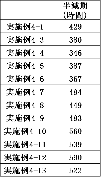
Claims (10)
- 式(1)で表される化合物からなる電荷輸送性物質と、分子量200~9,000の電荷輸送性化合物(ただし、前記式(1)で表される化合物を除く)からなる電荷輸送性物質とを含むことを特徴とする電荷輸送性材料。

- 前記電荷輸送性化合物が、アリールアミン誘導体、チオフェン誘導体およびピロール誘導体から選ばれる少なくとも1種である請求項1記載の電荷輸送性材料。
- さらにドーパント物質を含む請求項1または2記載の電荷輸送性材料。
- 請求項1~3のいずれか1項記載の電荷輸送性材料、および有機溶媒を含み、
前記電荷輸送性材料が、前記有機溶媒に溶解している電荷輸送性ワニス。 - さらに有機シラン化合物を含む請求項4記載の電荷輸送性ワニス。
- 請求項4または5記載の電荷輸送性ワニスを用いて作製される電荷輸送性薄膜。
- 請求項6記載の電荷輸送性薄膜を有する有機エレクトロルミネッセンス素子。
- 請求項4または5記載の電荷輸送性ワニスを基材上に塗布し、乾燥させることを特徴とする電荷輸送性薄膜の製造方法。
- 式(1)で表される化合物を用いて形成される電荷輸送性薄膜の平坦化方法であって、
式(1)で表される化合物からなる電荷輸送性物質と、分子量200~9,000の電荷輸送性化合物(ただし、前記式(1)で表される化合物を除く)からなる電荷輸送性物質とを含む電荷輸送性材料、および有機溶媒を含み、
前記電荷輸送性材料が前記有機溶媒に溶解している電荷輸送性ワニスを用いることを特徴とする電荷輸送性薄膜の平坦化方法。

- 陽極および陰極と、これら各極間に介在する発光層、正孔注入層および正孔輸送層を含む複数の機能層と、を有する有機エレクトロルミネッセンス素子の駆動電圧の低減方法であって、
式(1)で表される化合物からなる電荷輸送性物質と、分子量200~9,000の電荷輸送性化合物(ただし、前記式(1)で表される化合物を除く)からなる電荷輸送性物質とを含む電荷輸送性材料、および有機溶媒を含み、
前記電荷輸送性材料が前記有機溶媒に溶解している電荷輸送性ワニスを用いることを特徴とする有機エレクトロルミネッセンス素子の駆動電圧の低減方法。

Priority Applications (5)
| Application Number | Priority Date | Filing Date | Title |
|---|---|---|---|
| EP15825133.0A EP3174115B1 (en) | 2014-07-23 | 2015-07-21 | Charge transport material |
| US15/328,405 US10153439B2 (en) | 2014-07-23 | 2015-07-21 | Charge transport material |
| JP2016535928A JP6593334B2 (ja) | 2014-07-23 | 2015-07-21 | 電荷輸送性ワニス |
| KR1020177004703A KR102359651B1 (ko) | 2014-07-23 | 2015-07-21 | 전하 수송성 재료 |
| CN201580039951.2A CN106575709B (zh) | 2014-07-23 | 2015-07-21 | 电荷传输性材料 |
Applications Claiming Priority (4)
| Application Number | Priority Date | Filing Date | Title |
|---|---|---|---|
| JP2014150227 | 2014-07-23 | ||
| JP2014-150227 | 2014-07-23 | ||
| JP2015028392 | 2015-02-17 | ||
| JP2015-028392 | 2015-02-17 |
Publications (1)
| Publication Number | Publication Date |
|---|---|
| WO2016013533A1 true WO2016013533A1 (ja) | 2016-01-28 |
Family
ID=55163058
Family Applications (1)
| Application Number | Title | Priority Date | Filing Date |
|---|---|---|---|
| PCT/JP2015/070637 Ceased WO2016013533A1 (ja) | 2014-07-23 | 2015-07-21 | 電荷輸送性材料 |
Country Status (7)
| Country | Link |
|---|---|
| US (1) | US10153439B2 (ja) |
| EP (1) | EP3174115B1 (ja) |
| JP (1) | JP6593334B2 (ja) |
| KR (1) | KR102359651B1 (ja) |
| CN (1) | CN106575709B (ja) |
| TW (1) | TWI707856B (ja) |
| WO (1) | WO2016013533A1 (ja) |
Cited By (3)
| Publication number | Priority date | Publication date | Assignee | Title |
|---|---|---|---|---|
| CN111868029A (zh) * | 2018-03-16 | 2020-10-30 | 日产化学株式会社 | 苯胺衍生物的制造方法 |
| JP2023026298A (ja) * | 2021-08-13 | 2023-02-24 | 日本放送協会 | 電子素子用基板、有機エレクトロルミネッセンス素子、表示装置、及び照明装置 |
| JP2023026239A (ja) * | 2021-08-13 | 2023-02-24 | 日本放送協会 | 電子素子、有機エレクトロルミネッセンス素子、表示装置、及び照明装置 |
Families Citing this family (3)
| Publication number | Priority date | Publication date | Assignee | Title |
|---|---|---|---|---|
| DE102010045405A1 (de) * | 2010-09-15 | 2012-03-15 | Merck Patent Gmbh | Materialien für organische Elektrolumineszenzvorrichtungen |
| US10090477B2 (en) | 2014-05-23 | 2018-10-02 | Nissan Chemical Industries, Ltd. | Charge-transporting varnish |
| KR102892881B1 (ko) * | 2020-05-29 | 2025-11-28 | 삼성디스플레이 주식회사 | 정공 수송성 잉크 조성물, 발광 소자 및 이의 제조 방법 |
Citations (8)
| Publication number | Priority date | Publication date | Assignee | Title |
|---|---|---|---|---|
| JP2003519432A (ja) * | 1999-12-31 | 2003-06-17 | エルジー・ケミカル・カンパニー・リミテッド | p−型半導体性質を有する有機化合物を含む電子素子 |
| WO2008129947A1 (ja) * | 2007-04-12 | 2008-10-30 | Nissan Chemical Industries, Ltd. | オリゴアニリン化合物 |
| WO2010041701A1 (ja) * | 2008-10-09 | 2010-04-15 | 日産化学工業株式会社 | 電荷輸送性ワニス |
| WO2013077344A1 (ja) * | 2011-11-22 | 2013-05-30 | ユー・ディー・シー アイルランド リミテッド | 有機電界発光素子、有機電界発光素子用材料、並びに、該素子を用いた発光装置、表示装置、照明装置及び該素子に用いられる化合物 |
| JP2013527557A (ja) * | 2010-03-25 | 2013-06-27 | ユニバーサル ディスプレイ コーポレイション | 溶液加工可能な、ドープされたトリアリールアミン正孔注入材料 |
| WO2013122182A1 (ja) * | 2012-02-15 | 2013-08-22 | 国立大学法人山形大学 | 有機エレクトロルミネッセンス素子 |
| JP2014131057A (ja) * | 2008-11-19 | 2014-07-10 | Nissan Chem Ind Ltd | 電荷輸送性材料 |
| JP2015153864A (ja) * | 2014-02-13 | 2015-08-24 | 国立大学法人山形大学 | 有機膜及びこれを用いた有機電子デバイス |
Family Cites Families (9)
| Publication number | Priority date | Publication date | Assignee | Title |
|---|---|---|---|---|
| TW200615254A (en) | 2004-08-31 | 2006-05-16 | Nissan Chemical Ind Ltd | Arylsulfonic acid compound and use thereof as electron-acceptor material |
| EP2062870B1 (en) | 2006-09-13 | 2016-11-09 | Nissan Chemical Industries, Ltd. | Oligoaniline compounds |
| US20090091242A1 (en) * | 2007-10-05 | 2009-04-09 | Liang-Sheng Liao | Hole-injecting layer in oleds |
| EP2441750A4 (en) * | 2009-12-16 | 2012-12-12 | Idemitsu Kosan Co | AROMATIC AMINE DERIVATIVE AND ORGANIC ELECTROLUMINESCENT ELEMENT THEREWITH |
| KR101647134B1 (ko) * | 2010-03-29 | 2016-08-10 | 삼성디스플레이 주식회사 | 유기 발광 소자 |
| TW201228066A (en) * | 2010-12-31 | 2012-07-01 | Au Optronics Corp | Organic electroluminescent device |
| JP2014033008A (ja) | 2012-08-01 | 2014-02-20 | Sumitomo Chemical Co Ltd | 電荷受容性組成物及び有機エレクトロルミネッセンス素子 |
| WO2014097813A1 (ja) * | 2012-12-17 | 2014-06-26 | 新日鉄住金化学株式会社 | 有機電界発光素子 |
| DE102013114047B4 (de) | 2012-12-28 | 2016-09-01 | Lg Display Co., Ltd. | Organische lichtemittierende Anzeigevorrichtungen |
-
2015
- 2015-07-21 EP EP15825133.0A patent/EP3174115B1/en not_active Ceased
- 2015-07-21 US US15/328,405 patent/US10153439B2/en not_active Expired - Fee Related
- 2015-07-21 CN CN201580039951.2A patent/CN106575709B/zh active Active
- 2015-07-21 KR KR1020177004703A patent/KR102359651B1/ko active Active
- 2015-07-21 JP JP2016535928A patent/JP6593334B2/ja active Active
- 2015-07-21 WO PCT/JP2015/070637 patent/WO2016013533A1/ja not_active Ceased
- 2015-07-23 TW TW104123892A patent/TWI707856B/zh active
Patent Citations (8)
| Publication number | Priority date | Publication date | Assignee | Title |
|---|---|---|---|---|
| JP2003519432A (ja) * | 1999-12-31 | 2003-06-17 | エルジー・ケミカル・カンパニー・リミテッド | p−型半導体性質を有する有機化合物を含む電子素子 |
| WO2008129947A1 (ja) * | 2007-04-12 | 2008-10-30 | Nissan Chemical Industries, Ltd. | オリゴアニリン化合物 |
| WO2010041701A1 (ja) * | 2008-10-09 | 2010-04-15 | 日産化学工業株式会社 | 電荷輸送性ワニス |
| JP2014131057A (ja) * | 2008-11-19 | 2014-07-10 | Nissan Chem Ind Ltd | 電荷輸送性材料 |
| JP2013527557A (ja) * | 2010-03-25 | 2013-06-27 | ユニバーサル ディスプレイ コーポレイション | 溶液加工可能な、ドープされたトリアリールアミン正孔注入材料 |
| WO2013077344A1 (ja) * | 2011-11-22 | 2013-05-30 | ユー・ディー・シー アイルランド リミテッド | 有機電界発光素子、有機電界発光素子用材料、並びに、該素子を用いた発光装置、表示装置、照明装置及び該素子に用いられる化合物 |
| WO2013122182A1 (ja) * | 2012-02-15 | 2013-08-22 | 国立大学法人山形大学 | 有機エレクトロルミネッセンス素子 |
| JP2015153864A (ja) * | 2014-02-13 | 2015-08-24 | 国立大学法人山形大学 | 有機膜及びこれを用いた有機電子デバイス |
Non-Patent Citations (1)
| Title |
|---|
| See also references of EP3174115A4 * |
Cited By (4)
| Publication number | Priority date | Publication date | Assignee | Title |
|---|---|---|---|---|
| CN111868029A (zh) * | 2018-03-16 | 2020-10-30 | 日产化学株式会社 | 苯胺衍生物的制造方法 |
| JP2023026298A (ja) * | 2021-08-13 | 2023-02-24 | 日本放送協会 | 電子素子用基板、有機エレクトロルミネッセンス素子、表示装置、及び照明装置 |
| JP2023026239A (ja) * | 2021-08-13 | 2023-02-24 | 日本放送協会 | 電子素子、有機エレクトロルミネッセンス素子、表示装置、及び照明装置 |
| JP7691884B2 (ja) | 2021-08-13 | 2025-06-12 | 日本放送協会 | 電子素子、有機エレクトロルミネッセンス素子、表示装置、及び照明装置 |
Also Published As
| Publication number | Publication date |
|---|---|
| US20170213986A1 (en) | 2017-07-27 |
| KR20170032446A (ko) | 2017-03-22 |
| JP6593334B2 (ja) | 2019-10-23 |
| EP3174115A1 (en) | 2017-05-31 |
| CN106575709A (zh) | 2017-04-19 |
| TW201619163A (zh) | 2016-06-01 |
| TWI707856B (zh) | 2020-10-21 |
| EP3174115B1 (en) | 2020-05-20 |
| JPWO2016013533A1 (ja) | 2017-05-25 |
| KR102359651B1 (ko) | 2022-02-08 |
| EP3174115A4 (en) | 2018-02-28 |
| CN106575709B (zh) | 2020-01-07 |
| US10153439B2 (en) | 2018-12-11 |
Similar Documents
| Publication | Publication Date | Title |
|---|---|---|
| KR102411286B1 (ko) | 아닐린 유도체 및 그 이용 | |
| JP6593334B2 (ja) | 電荷輸送性ワニス | |
| JP6717372B2 (ja) | 電荷輸送性ワニス | |
| KR102408597B1 (ko) | 아닐린 유도체 및 그 이용 | |
| JP6011723B2 (ja) | トリフェニルアミン誘導体およびその利用 | |
| JP6128213B2 (ja) | チオフェン誘導体及びその利用並びにチオフェン誘導体の製造方法 | |
| JP6061034B2 (ja) | アニリン誘導体、電荷輸送性ワニス及び有機エレクトロルミネッセンス素子 | |
| JP6665853B2 (ja) | 有機エレクトロルミネッセンス素子用の電荷輸送性薄膜形成組成物、有機エレクトロルミネッセンス素子用の電荷輸送性薄膜及び有機エレクトロルミネッセンス素子 | |
| JP6551395B2 (ja) | アニリン誘導体およびその利用 |
Legal Events
| Date | Code | Title | Description |
|---|---|---|---|
| 121 | Ep: the epo has been informed by wipo that ep was designated in this application |
Ref document number: 15825133 Country of ref document: EP Kind code of ref document: A1 |
|
| ENP | Entry into the national phase |
Ref document number: 2016535928 Country of ref document: JP Kind code of ref document: A |
|
| NENP | Non-entry into the national phase |
Ref country code: DE |
|
| REEP | Request for entry into the european phase |
Ref document number: 2015825133 Country of ref document: EP |
|
| WWE | Wipo information: entry into national phase |
Ref document number: 2015825133 Country of ref document: EP Ref document number: 15328405 Country of ref document: US |
|
| ENP | Entry into the national phase |
Ref document number: 20177004703 Country of ref document: KR Kind code of ref document: A |