WO2016016968A1 - 電子装置及び電子装置の製造方法 - Google Patents
電子装置及び電子装置の製造方法 Download PDFInfo
- Publication number
- WO2016016968A1 WO2016016968A1 PCT/JP2014/070085 JP2014070085W WO2016016968A1 WO 2016016968 A1 WO2016016968 A1 WO 2016016968A1 JP 2014070085 W JP2014070085 W JP 2014070085W WO 2016016968 A1 WO2016016968 A1 WO 2016016968A1
- Authority
- WO
- WIPO (PCT)
- Prior art keywords
- conductor
- waveguide
- electronic device
- pin
- forming
- Prior art date
- Legal status (The legal status is an assumption and is not a legal conclusion. Google has not performed a legal analysis and makes no representation as to the accuracy of the status listed.)
- Ceased
Links
Images


Classifications
-
- H—ELECTRICITY
- H01—ELECTRIC ELEMENTS
- H01P—WAVEGUIDES; RESONATORS, LINES, OR OTHER DEVICES OF THE WAVEGUIDE TYPE
- H01P5/00—Coupling devices of the waveguide type
- H01P5/08—Coupling devices of the waveguide type for linking dissimilar lines or devices
- H01P5/10—Coupling devices of the waveguide type for linking dissimilar lines or devices for coupling balanced lines or devices with unbalanced lines or devices
- H01P5/103—Hollow-waveguide/coaxial-line transitions
-
- H—ELECTRICITY
- H01—ELECTRIC ELEMENTS
- H01P—WAVEGUIDES; RESONATORS, LINES, OR OTHER DEVICES OF THE WAVEGUIDE TYPE
- H01P11/00—Apparatus or processes specially adapted for manufacturing waveguides or resonators, lines, or other devices of the waveguide type
- H01P11/001—Manufacturing waveguides or transmission lines of the waveguide type
- H01P11/002—Manufacturing hollow waveguides
-
- H—ELECTRICITY
- H01—ELECTRIC ELEMENTS
- H01P—WAVEGUIDES; RESONATORS, LINES, OR OTHER DEVICES OF THE WAVEGUIDE TYPE
- H01P3/00—Waveguides; Transmission lines of the waveguide type
- H01P3/02—Waveguides; Transmission lines of the waveguide type with two longitudinal conductors
- H01P3/06—Coaxial lines
-
- H—ELECTRICITY
- H01—ELECTRIC ELEMENTS
- H01P—WAVEGUIDES; RESONATORS, LINES, OR OTHER DEVICES OF THE WAVEGUIDE TYPE
- H01P3/00—Waveguides; Transmission lines of the waveguide type
- H01P3/12—Hollow waveguides
-
- H—ELECTRICITY
- H01—ELECTRIC ELEMENTS
- H01Q—ANTENNAS, i.e. RADIO AERIALS
- H01Q13/00—Waveguide horns or mouths; Slot antennas; Leaky-waveguide antennas; Equivalent structures causing radiation along the transmission path of a guided wave
- H01Q13/10—Resonant slot antennas
-
- H—ELECTRICITY
- H10—SEMICONDUCTOR DEVICES; ELECTRIC SOLID-STATE DEVICES NOT OTHERWISE PROVIDED FOR
- H10W—GENERIC PACKAGES, INTERCONNECTIONS, CONNECTORS OR OTHER CONSTRUCTIONAL DETAILS OF DEVICES COVERED BY CLASS H10
- H10W44/00—Electrical arrangements for controlling or matching impedance
- H10W44/20—Electrical arrangements for controlling or matching impedance at high-frequency [HF] or radio frequency [RF]
- H10W44/241—Electrical arrangements for controlling or matching impedance at high-frequency [HF] or radio frequency [RF] for passive devices or passive elements
- H10W44/248—Electrical arrangements for controlling or matching impedance at high-frequency [HF] or radio frequency [RF] for passive devices or passive elements for antennas
-
- H—ELECTRICITY
- H10—SEMICONDUCTOR DEVICES; ELECTRIC SOLID-STATE DEVICES NOT OTHERWISE PROVIDED FOR
- H10W—GENERIC PACKAGES, INTERCONNECTIONS, CONNECTORS OR OTHER CONSTRUCTIONAL DETAILS OF DEVICES COVERED BY CLASS H10
- H10W72/00—Interconnections or connectors in packages
- H10W72/01—Manufacture or treatment
- H10W72/0198—Manufacture or treatment batch processes
-
- H—ELECTRICITY
- H10—SEMICONDUCTOR DEVICES; ELECTRIC SOLID-STATE DEVICES NOT OTHERWISE PROVIDED FOR
- H10W—GENERIC PACKAGES, INTERCONNECTIONS, CONNECTORS OR OTHER CONSTRUCTIONAL DETAILS OF DEVICES COVERED BY CLASS H10
- H10W72/00—Interconnections or connectors in packages
- H10W72/20—Bump connectors, e.g. solder bumps or copper pillars; Dummy bumps; Thermal bumps
- H10W72/241—Dispositions, e.g. layouts
-
- H—ELECTRICITY
- H10—SEMICONDUCTOR DEVICES; ELECTRIC SOLID-STATE DEVICES NOT OTHERWISE PROVIDED FOR
- H10W—GENERIC PACKAGES, INTERCONNECTIONS, CONNECTORS OR OTHER CONSTRUCTIONAL DETAILS OF DEVICES COVERED BY CLASS H10
- H10W72/00—Interconnections or connectors in packages
- H10W72/90—Bond pads, in general
- H10W72/941—Dispositions of bond pads
- H10W72/9413—Dispositions of bond pads on encapsulations
Definitions
- the present invention relates to an electronic device and a method for manufacturing the electronic device.
- a technique using a waveguide for signal transmission of an electronic device is known.
- a semiconductor device in which a waveguide is provided above or below a semiconductor chip, and a transmission antenna and a reception antenna that are electrically connected to the semiconductor chip are provided in the waveguide without contact with the waveguide Has been proposed.
- Waveguides enable signal transmission with lower loss than planar transmission lines.
- the size of the waveguide capable of signal transmission with low loss increases, and it may be difficult to obtain a small electronic device including the waveguide.
- a substrate having a terminal, a lower conductor provided above the substrate and having an opening at a position corresponding to the terminal, and an upper conductor disposed above the lower conductor;
- an electronic device including a waveguide including: a columnar conductor that is provided above the terminal, passes through the opening in a non-contact manner with the lower conductor, and is connected to the upper conductor.
- a step of preparing a substrate having a terminal, a lower conductor having an opening at a position corresponding to the terminal above the substrate, and an upper portion disposed above the lower conductor Forming a waveguide including a conductor, wherein the step of forming the waveguide is connected to the upper conductor through the opening without contacting the lower conductor and above the terminal.
- FIG. 3 is a first diagram illustrating an analysis example of transmission characteristics of an electronic device.
- FIG. 10 is a second diagram illustrating an analysis example of transmission characteristics of an electronic device. It is FIG. (1) which shows the example of an analysis of the transmission characteristic of a waveguide conversion part. It is FIG. (2) which shows the example of an analysis of the transmission characteristic of a waveguide conversion part. It is explanatory drawing (the 1) of an example of a conductor pin design method. It is explanatory drawing (the 2) of an example of a conductor pin design method.
- FIG. (1) shows an example of the formation method of an electronic device provided with a waveguide.
- FIG. (2) which shows an example of the formation method of an electronic device provided with a waveguide.
- FIG. (3) which shows an example of the formation method of an electronic device provided with a waveguide.
- FIG. (4) which shows an example of the formation method of an electronic device provided with a waveguide.
- FIG. (5) which shows an example of the formation method of an electronic device provided with a waveguide. It is FIG.
- FIG. (6) which shows an example of the formation method of an electronic device provided with a waveguide.
- FIG. (7) which shows an example of the formation method of an electronic device provided with a waveguide.
- FIG. (8) which shows an example of the formation method of an electronic device provided with a waveguide.
- FIG. (1) which shows another example of the formation method of an electronic device provided with a waveguide.
- FIG. (2) which shows another example of the formation method of an electronic device provided with a waveguide.
- FIG. (2) which shows another example of the formation method of an electronic device provided with a waveguide.
- FIG. (2) which shows another example of the formation method of an electronic device provided with a waveguide.
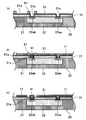
- FIG. 1 is an explanatory diagram of one embodiment of a waveguide.
- FIG. 1A is a schematic perspective view of an essential part of one embodiment of a waveguide
- FIG. 1B is a schematic cross-sectional view of a plane X in FIG.
- 1A and 1B includes a lower conductor 110, an upper conductor 120, and a sidewall conductor 130.
- An upper conductor 120 is provided to face the lower conductor 110, and the lower conductor 110 and the upper conductor 120 are connected by a side wall conductor 130.
- the inside of the waveguide 100 is hollow, for example.
- the waveguide 100 is mounted on a device (electronic device) such as a semiconductor chip or a semiconductor device including the semiconductor chip, and is a signal line drawn from the device side, for example, as shown in FIGS. 1A and 1B.
- a coaxial signal line (coaxial signal line) 200 is connected.
- the coaxial signal line 200 includes a center conductor 210 and a covered conductor 230 provided around the center conductor 210 via an insulating material 220. Such a coaxial signal line 200 is connected to the waveguide 100, and signal transmission (mode conversion) is performed with the waveguide 100.
- the coaxial signal line 200 exposes the central conductor 210 in the waveguide 100 in a non-contact manner with the waveguide 100 in order to convert a transmission signal between the coaxial signal line 200 and the waveguide 100. Connected.
- the length I of the central conductor 210 exposed in the waveguide 100 is, for example, about 1 ⁇ 4 wavelength of the transmission signal.
- the width a of the waveguide 100 is set based on the frequency of the transmission signal, and the thickness b of the waveguide 100 is often about half of the width a as a standard. For transmission of high-frequency signals exceeding millimeter waves, low-loss signal transmission can be performed by using the hollow waveguide 100.
- the size (thickness) of the waveguide 100 is exposed.
- the module including the waveguide 100 may become large in size.
- FIG. 2 is an explanatory view of another form of the waveguide.
- FIG. 2A is a schematic perspective view of an essential part of another form of the waveguide
- FIG. 2B is a schematic cross-sectional view of the plane Y of FIG. 2A and 2B illustrate a waveguide 100a that is thinner than the waveguide 100 illustrated in FIGS. 1A and 1B.
- the distance between the lower conductor 110 and the upper conductor 120 is narrower than that of the waveguide 100, and the length I of the central conductor 210 of the coaxial signal line 200 exposed in the waveguide 100a.
- the structure is shortened.
- a waveguide capable of low-loss signal transmission and suppressing an increase in the size of a module, and an electronic device including such a waveguide will be described.
- a waveguide according to an embodiment of the present invention and an electronic device including the waveguide will be described in detail.
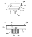
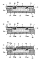
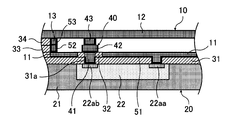
- FIG. 3 is a diagram illustrating an example of an electronic device.
- FIG. 3A is a schematic plan view of an essential part of an example of an electronic apparatus
- FIG. 3B is a schematic cross-sectional view of an essential part of an example of an electronic apparatus.
- 3A is a schematic plan view of the position along the line P2-P2 in FIG. 3B
- FIG. 3B is a cross-sectional view at the position along the line P1-P1 in FIG. It is a schematic diagram.
- the electronic device 1 illustrated in FIGS. 3A and 3B includes a substrate 20 and a waveguide 10.
- the waveguide 10 includes a lower conductor 11, an upper conductor 12, and a sidewall conductor 13.
- An upper conductor 12 is provided so as to face the lower conductor 11, and the lower conductor 11 and the upper conductor 12 are connected by a side wall conductor 13.
- the inside of the waveguide 10 is hollow.
- An insulating layer 30 is provided outside the waveguide 10.
- the waveguide 10 is provided above the substrate 20.
- a pseudo SoC (System20on Chip) substrate is illustrated as an example of the substrate 20.
- the substrate 20 may be before dicing or after dicing.
- the substrate 20 includes a resin layer 21 and a semiconductor chip 22 embedded in the resin layer 21.
- the semiconductor chip 22 has a plurality of terminals 22a.
- a ground (GND) terminal 22aa and a signal terminal 22ab are illustrated.
- the semiconductor chip 22 is embedded in the resin layer 21 so that the GND terminal 22aa and the signal terminal 22ab (terminal 22a) are exposed on the surface 21a side of the resin layer 21.
- the substrate on which the waveguide 10 is provided is not limited to a pseudo SoC substrate including the resin layer 21 and the semiconductor chip 22 such as the substrate 20, and may be a semiconductor chip, an interposer, a circuit substrate, or the like.
- the lower conductor 11 of the waveguide 10 is provided above the substrate 20 via an insulating layer 30 and is electrically connected to the GND terminal 22aa of the semiconductor chip 22 of the substrate 20.
- the lower conductor 11 is provided with an opening 11a at a position corresponding to the signal terminal 22ab of the semiconductor chip 22.
- Conductor pins (columnar conductors) 40 are provided on the signal terminals 22ab corresponding to the openings 11a.
- the conductor pin 40 is provided from the signal terminal 22ab side so as to pass through the opening 11a of the lower conductor 11 and further extend to the upper conductor 12 side, and the upper end reaches the upper conductor 12.
- the conductor pin 40 is connected to the lower conductor 41 provided on the signal terminal 22ab, the intermediate pin 42 provided on the pin 41, and further provided on the pin 42 to the upper conductor 12 (short circuit). And an upper layer pin 43 formed thereon.
- the pin 41 is provided at a height from the signal terminal 22ab to the upper surface of the lower conductor 11 (the opening 11a thereof), and the pin 42 has a height divided into two from the upper surface of the lower conductor 11 to the lower surface of the upper conductor 12.
- the case where the pin 43 is provided is illustrated.
- the diameters (widths of the cross section in the plane direction) of the pins 41, 42, and 43 of the conductor pins 40 can be set to desired values, respectively.
- a case where the pin 42 has a larger diameter than the pin 41 and the pin 43 has a smaller diameter than the pin 42 is illustrated.
- the cross-sectional shape in the planar direction of the pin 41, the pin 42, and the pin 43 of the conductor pin 40 is not limited to a circular shape, and various shapes such as a substantially circular shape, an elliptical shape, a substantially elliptical shape, a rectangular shape, and a substantially rectangular shape. Is possible.
- the number of layers of the conductor pin 40 connecting the signal terminal 22ab of the semiconductor chip 22 and the upper conductor 12 of the waveguide 10 is limited to three layers such as the pin 41, the pin 42, and the pin 43 described above.
- the number of layers can be set to one layer or two or more layers.
- a case where the number of pin layers of the conductor pin 40 is three is taken as an example.
- signal transmission is performed between the waveguide 10 and the substrate 20 (the signal terminal 22ab of the semiconductor chip 22) as described above.
- the distance from the lower conductor 11 to the upper conductor 12 of the waveguide 10, that is, the thickness (height) of the waveguide 10 is, for example, 1 ⁇ 4 of the signal transmitted between the semiconductor chip 22 and the waveguide 10. It can be made below the wavelength.
- the impedance on the semiconductor chip 22 side and the impedance on the waveguide 10 side can be adjusted (matched) by the diameters of the pin 41, the pin 42, and the pin 43 of the conductor pin 40.
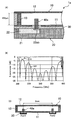
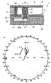
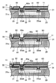
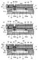
- FIG. 4 and 5 are diagrams illustrating examples of analysis of transmission characteristics of the electronic device.
- FIG. 4 shows an electronic device 1a in which the conductor pin 40a provided on the signal terminal 22ab of the semiconductor chip 22 and the upper conductor 12 of the waveguide 10 are not connected (short-circuited) (the waveguide of FIG. 1 above).
- 100 corresponds to an electronic device provided with 100).
- a cross section of the main part of such an electronic device 1a is schematically shown in FIG.
- the thickness of the waveguide 10 (the distance between the lower conductor 11 and the upper conductor 12) is 432 ⁇ m.
- FIG. 4B is an example of an electromagnetic field analysis result of such an electronic device 1a.
- FIG. 4A shows an electronic device 1a in which the conductor pin 40a provided on the signal terminal 22ab of the semiconductor chip 22 and the upper conductor 12 of the waveguide 10 are not connected (short-circuited) (the waveguide of FIG. 1 above).
- 100 corresponds to an electronic device provided with 100).
- FIG. 4B shows an electromagnetic field analysis when the distance between the conductor pins 40a provided in the two ports (Ports 1 and 2) of the waveguide 10 is set to 3 mm as shown in FIG. 1 shows an example of the relationship between the frequency (Frequency [GHz]) obtained in step S and the S parameter (S parameter [dB]).
- S11 is used for evaluation of reflection characteristics
- S21 is used for evaluation of transmission characteristics.
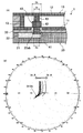
- FIG. 5 shows an analysis example of the electronic device 1 of FIG. 3 in which the conductor pin 40 provided on the signal terminal 22ab of the semiconductor chip 22 and the upper conductor 12 of the waveguide 10 are connected (short-circuited). Yes.
- a cross section of the main part of the electronic device 1 is schematically shown in FIG.
- the thickness of the waveguide 10 (the distance between the lower conductor 11 and the upper conductor 12) is 40 ⁇ m.
- FIG. 5B is an example of an electromagnetic field analysis result of such an electronic device 1.
- FIG. 5B shows an electromagnetic field analysis in the case where the distance between the conductor pins 40 provided in the two ports (Port 1, 2) of the waveguide 10 is set to 3 mm as shown in FIG. 5C.
- step S shows an example of the relationship between the frequency (Frequency [GHz]) obtained in step S and the S parameter (S parameter [dB]).
- S11 is used for evaluating the reflection characteristic of the transmission signal
- S21 is used for evaluating the transmission characteristic of the transmission signal.
- the S parameters (S11, S21) shown in FIGS. 4B and 5B are values (dB) obtained by taking the logarithm of the absolute value
- S absolute value
- the thickness of the waveguide 10 is about 1/10. 4B and 5B
- the transmission loss of the electronic device 1 (FIG. 5A) in which the conductor pin 40 is short-circuited to the waveguide 10 is the electronic device 1a (FIG. 4A) that is not short-circuited. It can be said that it is equivalent to the transmission loss of)).
- the thickness of the waveguide 10 can be reduced to about 1/10 with a transmission loss equivalent to that of the electronic device 1a.
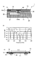
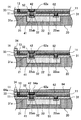
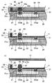
- FIG. 6 and 7 are diagrams illustrating an example of analysis of transmission characteristics of the waveguide converter.
- FIG. 6 illustrates a model of the conversion unit of the waveguide 10 having a different conductor pin shape.
- FIG. 6A shows a model corresponding to the waveguide 100 of FIG. 1, that is, a model A (Model A) in which the conductor pin 40 a is not short-circuited to the waveguide 10.
- FIGS. 6B and 6C are models in which the conductor pin 40 is short-circuited to the waveguide 10.
- FIG. 6B shows a model B in which a conductor pin 40 having a constant diameter is short-circuited to the waveguide 10
- FIG. 6C shows a conductor pin provided with parts having different diameters.
- a model C in which 40 is short-circuited to the waveguide 10 is shown.
- FIG. 7 shows the relationship between the frequency obtained by the electromagnetic field analysis and the S parameter for the input / output ports (Port 1, 2) of the converter in each of the models A to C in FIGS. 6 (A) to 6 (C).
- FIG. 7A shows an example of the relationship between the frequency (Frequency [GHz]) and S11 (S11 [dB])
- FIG. 7B shows the frequency (Frequency [GHz]) and S21 (S21 [ An example of the relationship of dB]) is shown.
- S11 is used for evaluating the reflection characteristic of the transmission signal
- S21 is used for evaluating the transmission characteristic of the transmission signal.
- the models B and C in which the conductor pin 40 is short-circuited to the waveguide 10 are compared with the model A in which the conductor pin 40a is not short-circuited to the waveguide 10.
- the value of S11, which is an index of the reflection characteristic, is low
- the value of S21, which is an index of the transmission characteristic is high.
- the transmission loss in the conversion part of the waveguide 10 can be suppressed as compared with the model A.
- the shape of the conductor pin 40 that is short-circuited to the waveguide 10 affects the reflection characteristics and transmission characteristics of the transmission signal. .
- the shape of the conductor pin 40 By adjusting the shape of the conductor pin 40, it is possible to adjust the reflection characteristic and the transmission characteristic in the conversion part of the waveguide 10. By performing such adjustment, it is possible to perform impedance matching between the waveguide 10 and the signal line (the signal terminal 22ab of the semiconductor chip 22 and the conductor pin 40).
- FIGS. 8 to 12 are explanatory diagrams of an example of a conductor pin design method.
- FIG. 8 is a diagram schematically showing an electronic device including a conductor pin and a waveguide in the initial stage of design.
- FIG. 8A is a schematic plan view of the main part of the electronic device
- FIG. 8B is a schematic cross-sectional view of the main part of the electronic device.
- the diameter Dp of the pin 41 provided on the signal terminal 22ab of the semiconductor chip 22 is set to an arbitrary constant value.
- the diameter Dp of the pin 41 can be set based on, for example, the planar size of the signal terminal 22ab.
- the pins 42 and 43 provided on the pins 41 are also set to the diameter Dp.
- the opening size (diameter) Dh of the opening 11a provided in the lower conductor 11 of the waveguide 10 is a characteristic when the pin 41, the insulating layer 30, and the lower conductor 11 are regarded as coaxial lines having the pin 41 as a central conductor.
- the diameter Dh can be set to a predetermined value such as 50 ⁇ .
- the thickness b and width a of the waveguide 10 can be set to arbitrary constant values. However, it is desirable to set based on the frequency of the signal to be transmitted. Further, the distance from the side wall conductor 13 to the conductor pin 40 (back stub length Lb) can be set to about 1 ⁇ 4 wavelength of a signal transmitted through the waveguide 10, for example.
- the diameter Dp of the conductor pin 40 (pin 41) is 100 ⁇ m, and the opening diameter Dh of the lower conductor 11 is 230 ⁇ m.
- the width a of the waveguide 10 is 864 ⁇ m, the thickness b is 40 ⁇ m, and the back stub length Lb is 300 ⁇ m.
- the diameters of the pin 42 and the pin 43 on the pin 41 are adjusted. In this adjustment, the lengths of the pins 41, 42, and 43 are not changed.
- FIG. 9 is an explanatory diagram of the first adjustment of the conductor pin.
- FIG. 9A is a schematic cross-sectional view of an essential part showing an example of the electronic device in the first adjustment stage
- FIG. 9B is a diagram showing an example of the Smith chart in the first adjustment stage.
- FIG. 9B shows a Smith chart of input impedance (normalized) viewed from the semiconductor chip 22 side.
- FIG. 10 is an explanatory diagram of the second adjustment of the conductor pin.
- FIG. 10A is a schematic cross-sectional view of an essential part showing an example of an electronic device in the second adjustment stage
- FIG. 10B is a diagram showing an example of a Smith chart in the second adjustment stage.
- FIG. 10B shows a Smith chart of input impedance (normalized) viewed from the semiconductor chip 22 side.
- the diameter Dt of the pin 43 is smaller than the diameter Db of the pin 42 directly below, the lower conductor 11 of the waveguide 10 and the pin 42 of the conductor pin 40 close thereto are The distance does not change. Therefore, the capacitance between the lower conductor 11 and the conductor pin 40 does not change or does not change greatly.
- the resistance value of the conductor pin 40 increases, and therefore the real part of the input impedance viewed from the semiconductor chip 22 side tends to increase. Indicates.
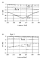
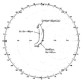
- FIG. 11 and 12 are explanatory diagrams of an example of impedance matching.
- FIG. 11 shows a Smith chart as an example when impedance matching is performed by performing the first adjustment as described in FIG. 9 and the second adjustment as described in FIG. .
- FIG. 12 shows an example of the relationship between the frequency (Frequency [GHz]) and the S parameter (S parameter [dB]) obtained by the electromagnetic field analysis after the unadjusted stage and after the first adjustment and the second adjustment.
- S11 is used for evaluating the reflection characteristic of the transmission signal
- S21 is used for evaluating the transmission characteristic of the transmission signal.
- the imaginary part of the input impedance of the pin 42 on the pin 41 and the diameter Db of the pin 43 becomes 0 near the frequency of the transmission signal. Or adjust so that it is almost zero.
- the diameter Dt of the upper pin 43 is adjusted so that the real part of the input impedance is 1 or close to 1 for such a conductor pin 40.
- the resistance value of the conductor pin 40 is increased, and the real part of the input impedance is mainly shifted in the increasing direction, and the real part becomes 1 or approaches 1, that is, impedance matching can be achieved. .
- Fine adjustment of the diameter may be performed.
- the first adjustment is performed from the unadjusted stage, and then the second adjustment is performed.
- the value of S21 which is an index of the passage characteristic, can be increased.
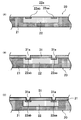
- FIGS. 13 to 20 schematically show a cross section of the main part of each forming process of the electronic device.
- a substrate 20 including a resin layer 21 and a semiconductor chip 22 embedded in the resin layer 21 is prepared.
- a filler filler
- the substrate 20 is formed by coating the periphery of the semiconductor chip 22 with the resin layer 21 so that the arrangement surface side of the terminals 22a (22aa, 22ab) is exposed, and then heat-molding it.
- another semiconductor chip or a chip component such as a chip capacitor may be further embedded in the resin layer 21 of the substrate 20.
- the substrate 20 for example, a wafer-like material (pseudo wafer) before dicing is used.
- a pseudo wafer obtained by dicing can be used.
- an insulating layer 31 (a part of the insulating layer 30) having an opening 31a communicating with the terminal 22a of the semiconductor chip 22 in the substrate 20 is formed.
- a photosensitive phenol resin is applied to the substrate 20 to a thickness of 10 ⁇ m, exposed to light, and then developed using tetramethylammonium hydroxide (TMAH) or the like.
- TMAH tetramethylammonium hydroxide
- curing is performed at a temperature of 200 ° C. to 250 ° C., for example, 200 ° C. to form an insulating layer 31 having an opening 31a as shown in FIG.
- a seed layer 51 is formed on the insulating layer 31 including the inside of the opening 31a.
- a titanium (Ti) layer is formed with a thickness of 20 nm on the insulating layer 31 by sputtering
- a copper (Cu) layer is further formed with a thickness of 100 nm on the Ti layer by sputtering, A seed layer 51 is formed.
- a resist pattern 61 having an opening 61 a corresponding to a region where the pin 41 of the conductor pin 40 and the lower conductor 11 of the waveguide 10 are formed is formed on the seed layer 51.
- a resist material is applied on the seed layer 51 with a thickness of 8 ⁇ m, and after exposure, the resist pattern 61 is formed by developing using TMAH or the like.
- the resist pattern 61 is formed in a region that separates the pin 41 and the lower conductor 11 formed on the signal terminal 22ab of the semiconductor chip 22.
- the lowermost pin 41 of the conductor pin 40 and the lower conductor 11 of the waveguide 10 are formed in the opening 61 a of the resist pattern 61.
- the pin 41 and the lower conductor 11 are formed by depositing Cu as a conductor material by electrolytic plating using the seed layer 51 as a power feeding layer.
- the height of the lower conductor 11 is, for example, 5 ⁇ m.
- the lower conductor 11 is connected to the GND terminal 22aa of the semiconductor chip 22.
- the pin 41 is connected to the signal terminal 22ab of the semiconductor chip 22.
- the resist pattern 61 and part of the seed layer 51 are removed.
- the resist pattern 61 is first removed using acetone or the like, and then the portion of the seed layer 51 exposed by removing the resist pattern 61 is removed.
- the seed layer 51 has a laminated structure in which a Cu layer is provided on the Ti layer as described above, the Cu layer is first selectively removed, and then the Ti layer is selectively removed.
- the Cu layer is selectively removed by wet etching using, for example, potassium sulfate (K 2 SO 4 ) as an etchant.
- K 2 SO 4 potassium sulfate
- the Ti layer is selectively removed by, for example, dry etching using a mixed gas of carbon tetrafluoride (CF 4 ) and oxygen (O 2 ).
- an insulating layer 32 (a part of the insulating layer 30) is formed in a region where the resist pattern 61 and a part of the seed layer 51 are removed.
- a photosensitive phenolic resin having a thickness of 5 ⁇ m is applied, exposed, developed using TMAH, etc., and cured at a temperature of 200 ° C.
- an insulating layer 33 (a part of the insulating layer 30) is formed in a region outside the waveguide 10 to be formed.
- a photosensitive phenol resin with a thickness of 10 ⁇ m is applied, exposed, developed with TMAH, etc., and cured at a temperature of 200 ° C.
- a sacrificial layer 62 having an opening 62a corresponding to a region where the pin 42 of the conductor pin 40 and the side wall conductor 13 of the waveguide 10 are formed is formed.
- a sacrificial layer 62 is formed by applying a resist material with a thickness of 10 ⁇ m, and developing after exposure using TMAH or the like.
- the opening 62 a of the sacrificial layer 62 the opening 62 a corresponding to the region where the pin 42 is formed is formed with a diameter based on the diameter of the pin 42 to be formed.
- FIG. 15C illustrates a case where the opening 62a having a larger diameter than the pin 41 on the signal terminal 22ab is formed.
- a seed layer 52 is formed on the sacrificial layer 62 including the inside of the opening 62a.
- the seed layer 52 is formed, for example, by forming a Ti layer and a Cu layer with a predetermined thickness by sputtering.
- a resist pattern 63 having an opening 63a corresponding to a region where the pin 42 of the conductor pin 40 and the side wall conductor 13 of the waveguide 10 are formed is formed on the seed layer 52.
- the resist pattern 63 is formed by, for example, applying a resist material with a thickness of 8 ⁇ m on the seed layer 52 and developing the resist pattern using TMAH or the like after exposure.
- the pin 42 (intermediate layer) of the conductor pin 40 and the sidewall conductor of the waveguide 10 are formed in the opening 62 a of the sacrificial layer 62 located in the opening 63 a of the resist pattern 63. 13 (lower layer) is formed.
- the pins 42 and the side wall conductors 13 are formed, for example, by depositing Cu by electrolytic plating using the seed layer 52 as a power feeding layer.
- the height of the pin 42 and the side wall conductor 13 formed here is, for example, 10 ⁇ m.
- the resist pattern 63 and a part of the seed layer 52 are removed.
- the resist pattern 63 is first removed using acetone or the like, and the portion of the seed layer 52 exposed after the removal is selectively removed by etching. By removing the seed layer 52, the pin 42 and the sidewall conductor 13 are electrically separated.
- an insulating layer 34 (a part of the insulating layer 30) is formed in a region outside the waveguide 10 to be formed.
- the insulating layer 34 is formed, for example, by first applying a photosensitive phenol-based resin with a thickness of 10 ⁇ m, developing after exposure using TMAH, and performing curing at a temperature of 200 ° C.
- a sacrificial layer 64 having an opening 64a corresponding to a region where the pin 43 of the conductor pin 40 and the sidewall conductor 13 of the waveguide 10 are formed is formed.
- the sacrificial layer 64 is formed by, for example, applying a resist material with a thickness of 10 ⁇ m, developing after exposure using TMAH or the like.
- the opening 64 a of the sacrificial layer 64 is formed with a diameter based on the diameter of the pin 43 to be formed.
- FIG. 17C illustrates the case where the opening 64a having a smaller diameter than the previously formed pin 42 is formed.
- a seed layer 53 is formed on the sacrificial layer 64 including the inside of the opening 64a.
- the seed layer 53 is formed, for example, by forming a Ti layer and a Cu layer with a predetermined thickness by sputtering.
- a resist pattern 65 having an opening 65 a corresponding to a region where the pin 43 of the conductor pin 40 and the side wall conductor 13 of the waveguide 10 are formed is formed on the seed layer 53.
- the resist pattern 65 is formed by, for example, applying a resist material with a thickness of 8 ⁇ m on the seed layer 53, developing after exposure using TMAH or the like.
- the pin 43 (upper layer) of the conductor pin 40 and the sidewall conductor of the waveguide 10 are formed in the opening 64 a of the sacrificial layer 64 located in the opening 65 a of the resist pattern 65. 13 (upper layer) is formed.
- the pin 43 and the side wall conductor 13 are formed by depositing Cu by, for example, electrolytic plating using the seed layer 53 as a power feeding layer.
- the height of the pin 43 and the side wall conductor 13 formed here is, for example, 10 ⁇ m.
- the resist pattern 65 is removed, and the seed layer 53 exposed after the removal is removed.
- the resist pattern 65 is removed using acetone or the like, and the seed layer 53 is selectively removed by etching. By removing the seed layer 53, the pin 43 and the sidewall conductor 13 are electrically separated.
- the sacrificial layer 62 and the sacrificial layer 64 are removed.
- the sacrificial layer 62 and the sacrificial layer 64 are removed using, for example, acetone.
- the hollow portion of the waveguide 10 is formed.
- the upper conductor 12 of the waveguide 10 is formed.
- a metal foil such as Cu is bonded on the insulating layer 34, the sidewall conductor 13, and the conductor pin 40 by lamination.
- the thickness of the metal foil is, for example, 20 ⁇ m.
- the resin layer 21 in which the semiconductor chip 22 is embedded and the waveguide 10 are integrated by performing the process up to the formation of the waveguide 10 as described above.
- a pseudo wafer is obtained.
- individual electronic devices 1 including the waveguides 10 are obtained by dicing into pieces by dicing using a diamond blade or the like.
- the electronic device 1 including the waveguide 10 is obtained by performing the formation up to the waveguide 10 as described above.
- the case where the conductor pin 40 having the three layers of the pin 41, the pin 42, and the pin 43 is formed is illustrated.
- the steps after FIG. 19B may be performed.
- the steps of FIGS. 17B to 19A are omitted after the step of FIG. 17A, and the sacrificial layer 62 is formed according to the example of FIG. 19B.
- the upper conductor 12 may be formed according to the example of FIG.
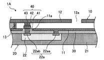
- FIG. 21 is a diagram illustrating another example of an electronic device.
- FIG. 21 schematically illustrates a cross section of a main part of another example of the electronic device.
- the electronic device 1A shown in FIG. 21 is different from the electronic device 1 shown in FIG. 3 and the like in that at least one slot 12a is provided in the upper conductor 12 of the waveguide 10.
- FIG. 21 illustrates one slot 12a, but the upper conductor 12 may be provided with a plurality of slots 12a. Further, the shape and position of the slot 12a, the arrangement (slot pattern) of the plurality of slots 12a, and the like can be set as appropriate based on characteristics such as the frequency of a signal to be transmitted or received.
- the waveguide 10 can have an antenna function as well as a signal transmission function.
- An electronic device 1A including a thin waveguide 10 that can transmit or receive signals, has a conversion unit in which the conductor pin 40 is short-circuited with the upper conductor 12, and suppresses transmission loss of the conversion unit is realized. be able to.
- Such an electronic device 1A can be formed, for example, according to the example described with reference to FIGS.
- the upper conductor 12 such as a metal foil provided with the slot 12a in advance is laminated with the insulating layer 30 ( 34) Adhere on the side wall conductor 13 and the conductor pin 40.
- the electronic device 1A can be formed using the following method.
- the process can be the same up to the step of forming the seed layer 53 in FIG. The subsequent forming process will be described with reference to FIGS.
- the pin 43 of the conductor pin 40, the side wall conductor 13 of the waveguide 10 and the upper conductor 12 are formed as shown in FIG. 22A.
- a resist pattern 65 having an opening 65a corresponding to the region to be formed is formed.
- the upper conductor having the pin 43 (upper layer) of the conductor pin 40, the side wall conductor 13 (upper layer) of the waveguide 10, and the slot 12a in the opening 65a of the resist pattern 65. 12 is formed.
- the pin 43, the sidewall conductor 13, and the upper conductor 12 are formed by depositing a conductor material such as Cu by electrolytic plating using the seed layer 53 as a power feeding layer.
- the resist pattern 65 is removed, and the seed layer 53 exposed after the removal is removed.
- the sacrificial layer 62 and the sacrificial layer 64 are removed using an etchant such as acetone, thereby forming the waveguide 10 having a hollow portion as shown in FIG.
- the etchant flows into the waveguide 10 through the slot 12 a of the upper conductor 12 and flows out of the waveguide 10, so that the sacrificial layer 62 and the sacrificial layer 64 are etched. And removed from the inside of the waveguide 10.
- the electronic device 1A including the waveguide 10 having the slot 12a can be obtained.
- slot patterns of various shapes, arrangements, and sizes can be formed with high accuracy.
- FIGS. 22A to 22C and FIG. 23 are performed after the step shown in FIG.
- the process up to the above-described step of FIG. 19A is performed, and the slot 12a is moved from the state where the pin 43 and the side wall conductor 13 are formed according to the procedure example of FIGS. 22A to 22C and FIG. You may make it form the upper conductor 12 which has.
- the upper end of the conductor pin 40 standing on the signal terminal 22ab of the semiconductor chip 22 is connected to the upper conductor 12 of the waveguide 10 having the lower conductor 11, the side wall conductor 13, and the upper conductor 12. And short-circuit.
- the diameter of the conductor pin 40 is adjusted so that impedance matching can be achieved between the semiconductor chip 22 and the waveguide 10. According to such a waveguide 10, low-loss signal transmission between the semiconductor chip 22 and the waveguide 10 is possible, and even a high-frequency signal exceeding millimeter waves can be transmitted with low loss. Become.
- the waveguide 10 can be formed by using the rewiring technique, and is wider than the wiring formed by the semiconductor process and has a thickness by the rewiring technique. It is possible to form a thin waveguide 10 that is about the insulating portion (insulating layer) of the redistribution layer. By forming such a waveguide 10, it is possible to realize a thin electronic device 1, 1 ⁇ / b> A with low transmission loss.
- the rewiring technique used in the heterogeneous device integration such as pseudo SoC as described above is an effective means for suppressing the loss in the transmission line connecting the elements. This is because according to the rewiring technique, it is possible to realize a transmission line having a relatively short transmission line length between the respective elements and a relatively wider transmission line than a semiconductor process.
- the frequency range is higher than that of millimeter waves
- the length of the transmission line cannot be ignored with respect to the wavelength, the conductor loss due to the skin effect increases, and the dielectric loss of the insulating material cannot be ignored. Can occur. Therefore, in such high-frequency signal transmission, it is effective to use a hollow waveguide for the transmission line.
- a wide and thin hollow waveguide 10 can be realized by using a rewiring technique, and a conductor to be short-circuited to the waveguide 10.
- Low loss signal transmission can be realized by adjusting the diameter of the pin 40. For example, when a signal having a frequency of 300 GHz is transmitted through a transmission line having a length of 1 mm, the transmission loss is -2.5 dB in the microstrip line, whereas the transmission loss is -0.5 dB in the hollow waveguide 10. Can be suppressed.
- a waveguide 10 used for transmission of a signal having a frequency of 300 GHz, a waveguide 10 having a width of 500 ⁇ m or more, a thickness of about 40 ⁇ m, and a pass characteristic of ⁇ 0.5 dB can be realized.
- the case where the inside of the waveguide 10 is hollow is illustrated, but a dielectric may be provided inside the waveguide 10.
- a pseudo SoC substrate is used as the substrate 20 is exemplified.
- the waveguide 10 as described above is not limited to a pseudo SoC substrate, but may be provided on a single semiconductor chip or a circuit board such as a printed board or an interposer. It can also be provided on top.
- FIG. 24 is a diagram illustrating an example of an electronic device including a waveguide provided on a semiconductor chip.
- FIG. 24A schematically illustrates a cross section of a main part of a first configuration example of an electronic device including a waveguide provided over a semiconductor chip
- tip is typically illustrated.
- An electronic device 1B shown in FIG. 24A includes a semiconductor chip 70 and a waveguide 10 provided on the semiconductor chip 70.
- the semiconductor chip 70 includes a semiconductor substrate 71 such as silicon (Si) and a wiring layer 72 provided on the semiconductor substrate 71. Circuit elements (not shown) such as transistors, resistors, and capacitors are formed on the surface of the semiconductor substrate 71 (the surface on which the wiring layer 72 is disposed).
- the wiring layer 72 includes a conductor portion (not shown) such as a wiring or a via electrically connected to a circuit element such as a transistor formed on the semiconductor substrate 71 and an insulating portion (around the conductor portion). (Not shown).
- a GND terminal 22aa and a signal terminal 22ab are provided in the uppermost conductor portion of the wiring layer 72.
- the waveguide 10 is provided on the wiring layer 72 of the semiconductor chip 70.
- the conductor pin 40 provided on the signal terminal 22ab is connected to the upper conductor 12 of the waveguide 10.
- the lower conductor 11 of the waveguide 10 is connected to the GND terminal 22aa.
- the electronic device 1 ⁇ / b> C illustrated in FIG. 24B includes the semiconductor chip 70 and the waveguide 10 provided on the semiconductor chip 70.
- a through electrode 73 that penetrates the semiconductor substrate 71 and is electrically connected to the wiring layer 72 provided on the surface (formation surface of a circuit element such as a transistor) is provided in the semiconductor chip 70. (Through Silicon Via) technology or the like.
- a GND terminal 22aa and a signal terminal 22ab are provided on the surface of the through electrode 73 opposite to the surface on which the wiring layer 72 is provided.
- the conductor pin 40 provided on the signal terminal 22ab is connected to the upper conductor 12 of the waveguide 10.
- the lower conductor 11 of the waveguide 10 is connected to the GND terminal 22aa.
- the waveguide 10 can be provided on the semiconductor chip 70, and in this case, the wiring layer 72 is disposed on the side of the wiring layer 72 or on the semiconductor substrate 71. It can be provided on the back surface (surface opposite to the surface on which the wiring layer 72 is disposed). Note that a slot (such as the above-described slot 12a) may be provided in the upper conductor 12 of the waveguide 10 so that the electronic device 1B and the electronic device 1C have an antenna function.
- FIG. 25 is a diagram showing an example of an electronic device including a waveguide provided on a circuit board.
- FIG. 25 schematically illustrates a cross section of a main part of a configuration example of an electronic device including a waveguide provided on a circuit board.
- the 25 includes a circuit board 80 and a waveguide 10 provided on the circuit board 80.
- the circuit board 80 includes a base material 81 and conductor portions 82 (wiring, vias, etc.) provided on the inside or the surface of the base material 81.
- a circuit board 80 in which the front and back surfaces (both main surfaces) are electrically connected by a conductor portion 82 is illustrated.
- the circuit board 80 may be, for example, a printed board or an interposer using an insulating material such as a resin for the base material 81, or may be a Si interposer using a semiconductor substrate such as Si for at least a part of the base material 81. .
- a GND terminal 22aa and a signal terminal 22ab are provided on the conductor portion 82 exposed on one surface side of the circuit board 80.
- the waveguide 10 is provided on such a circuit board 80.
- the conductor pin 40 provided on the signal terminal 22ab is connected to the upper conductor 12 of the waveguide 10.
- the lower conductor 11 of the waveguide 10 is connected to the GND terminal 22aa.
- the waveguide 10 can also be provided on a circuit board 80. It should be noted that the upper conductor 12 of the waveguide 10 may be provided with a slot (the above-described slot 12a or the like) so that the electronic device 1D has an antenna function.
Landscapes
- Engineering & Computer Science (AREA)
- Manufacturing & Machinery (AREA)
- Waveguides (AREA)
- Waveguide Aerials (AREA)
Abstract
Description
本発明の目的、特徴及び利点は、本発明の例として好ましい実施の形態を表す添付の図面と関連した以下の説明により明らかになるであろう。
図1は導波管の一形態の説明図である。図1(A)は導波管の一形態の要部斜視模式図、図1(B)は図1(A)の面Xの断面模式図である。
ミリ波を超える高周波信号の伝送には、中空の導波管100を用いることで、低損失の信号伝送が行える。
図2(A)及び図2(B)には、上記図1(A)及び図1(B)に示した導波管100よりも厚みを薄くした導波管100aを例示している。この導波管100aは、上記導波管100よりも、下部導体110と上部導体120の間隔を狭め、且つ、同軸信号線200の、導波管100a内に露出する中心導体210の長さIを短くした構造を有している。
以下、本発明の一実施形態に係る導波管、及び導波管を備えた電子装置について、詳細に説明する。
導波管10は、下部導体11、上部導体12、及び側壁導体13を含む。下部導体11に対向するように上部導体12が設けられ、下部導体11と上部導体12は、側壁導体13で連結されている。導波管10の内部は、中空になっている。導波管10の外側には、絶縁層30が設けられている。
また、導波管10を設ける基板は、この基板20のような樹脂層21と半導体チップ22を含む擬似SoC基板に限定されるものではなく、半導体チップ、インターポーザ、回路基板等でもよい。ここでは説明の便宜上、図3(B)に示すような擬似SoC基板を基板20の例とする。
ここで、図4には、半導体チップ22の信号端子22ab上に設けた導体ピン40aと導波管10の上部導体12を接続(短絡)させない形態の電子装置1a(上記図1の導波管100を設けた電子装置に相当)の解析例を示している。このような電子装置1aの要部断面を、図4(A)に模式的に図示している。図4(A)に示す電子装置1aにおいて、導波管10の厚み(下部導体11と上部導体12の間の距離)は、432μmとしている。図4(B)は、このような電子装置1aの電磁界解析結果の一例である。図4(B)には、図4(C)に示すような、導波管10の2ポート(Port 1, 2)に設けた導体ピン40a間の距離を3mmに設定した場合の電磁界解析で得られた周波数(Frequency [GHz])とSパラメータ(S parameter [dB])の関係の一例を示している。S11を反射特性の評価に用い、S21を通過特性の評価に用いる。
ここで、図6には、導体ピン形状の異なる導波管10の変換部のモデルを例示している。図6(A)には、上記図1の導波管100に相当するモデル、即ち導体ピン40aを導波管10に短絡させないモデルA(Model A)を示している。一方、図6(B)及び図6(C)は、導体ピン40を導波管10に短絡させたモデルである。図6(B)には、一定の径の導体ピン40を導波管10に短絡させたモデルB(Model B)を示し、図6(C)には、異なる径の部位を設けた導体ピン40を導波管10に短絡させたモデルC(Model C)を示している。
図8~図12は導体ピン設計方法の一例の説明図である。
このようなピン42及びピン43の径Dbの調整によってインピーダンス整合が取れない場合には、ピン42及びピン43のうち、上側のピン43の径を更に調整する。尚、この調整時には、ピン41、ピン42及びピン43の各々の長さは変化させない。
まず、図13(A)に示すような、樹脂層21、及び樹脂層21に埋設された半導体チップ22を含む基板20(擬似SoC基板)を準備する。基板20の樹脂層21には、例えば、エポキシ系の樹脂にシリカ等のフィラー(充填剤)を混合したものを用いる。基板20は、半導体チップ22の周囲をその端子22a(22aa,22ab)の配設面側が露出するように樹脂層21で被覆し、これを加熱成形することによって、形成する。尚、基板20の樹脂層21には、半導体チップ22のほか、別の半導体チップや、チップコンデンサ等のチップ部品が更に埋設されてもよい。
尚、ここでは、3層のピン41、ピン42及びピン43を有する導体ピン40を形成する場合を例示した。4層以上のピンを形成する場合には、図19(A)の工程後、図19(B)の工程前に、ピンの層数に応じた回数だけ図17(B)~図19(A)の工程を繰り返し、その後、図19(B)以降の工程を行うようにすればよい。
以上説明した導波管10には、アンテナ機能を設けることもできる。
図21は電子装置の別例を示す図である。図21には、電子装置の別例の要部断面を模式的に図示している。
電子装置1Aの形成では、例えば、上記電子装置1の形成方法として述べた図18(A)のシード層53の形成工程までは同じとすることができる。その後の形成工程について、図22及び図23を参照して説明する。
そして、アセトン等のエッチャントを用いて、犠牲層62及び犠牲層64を除去することで、図23に示すような、中空部を有する導波管10を形成する。犠牲層62及び犠牲層64の除去時には、エッチャントが、上部導体12のスロット12aを通して導波管10内に流入し、導波管10外に流出することで、犠牲層62及び犠牲層64がエッチングされ、導波管10内から除去される。
また、以上の説明では、基板20に擬似SoC基板を用いる場合を例示した。このほか、上記のような導波管10(アンテナ機能を有する導波管10を含む)は、擬似SoC基板に限らず、半導体チップ単体の上に設けたり、プリント基板やインターポーザ等の回路基板の上に設けたりすることもできる。
上記については単に本発明の原理を示すものである。更に、多数の変形、変更が当業者にとって可能であり、本発明は上記に示し、説明した正確な構成及び応用例に限定されるものではなく、対応する全ての変形例及び均等物は、添付の請求項及びその均等物による本発明の範囲とみなされる。
10,100,100a 導波管
11,110 下部導体
11a,31a,61a,62a,63a,64a,65a 開口部
12,120 上部導体
12a スロット
13,130 側壁導体
20,81 基板
21 樹脂層
21a 表面
22,70 半導体チップ
22a 端子
22aa GND端子
22ab 信号端子
30,31,32,33,34 絶縁層
40,40a 導体ピン
41,42,43 ピン
51,52,53 シード層
61,63,65 レジストパターン
62,64 犠牲層
71 半導体基板
72 配線層
73 貫通電極
80 回路基板
82 導体部
200 同軸信号線
210 中心導体
220 絶縁材料
230 被覆導体
Claims (15)
- 端子を有する基板と、
前記基板の上方に設けられ、前記端子に対応する位置に開口部を有する下部導体と、前記下部導体の上方に配置された上部導体とを含む導波管と、
前記端子の上方に設けられ、前記下部導体と非接触で前記開口部を貫通し、前記上部導体に接続される柱状導体と
を含むことを特徴とする電子装置。 - 前記下部導体から前記上部導体までの高さが、前記端子と前記導波管の間を伝送される信号の1/4波長以下であることを特徴とする請求項1に記載の電子装置。
- 前記柱状導体は、
前記端子側から前記開口部内に延びる第1導体部と、
前記第1導体部の上方に設けられ、前記上部導体に接続される第2導体部と
を含むことを特徴とする請求項1に記載の電子装置。 - 前記第2導体部は、前記第1導体部とは径が異なることを特徴とする請求項3に記載の電子装置。
- 前記第2導体部は、互いに径が異なる複数の部位を含むことを特徴とする請求項3に記載の電子装置。
- 前記開口部は、前記下部導体と前記柱状導体の前記開口部内に位置する部位とを同軸線とした時の特性インピーダンスが所定値となる径に設定されていることを特徴とする請求項1に記載の電子装置。
- 前記上部導体は、スロットを有することを特徴とする請求項1に記載の電子装置。
- 前記基板は、
樹脂層と、
前記端子を有し、前記樹脂層に埋設され、前記端子が前記樹脂層から露出する半導体素子と
を含むことを特徴とする請求項1に記載の電子装置。 - 前記導波管は、中空であることを特徴とする請求項1乃至8のいずれかに記載の電子装置。
- 端子を有する基板を準備する工程と、
前記基板の上方に、前記端子に対応する位置に開口部を有する下部導体と、前記下部導体の上方に配置された上部導体とを含む導波管を形成する工程と
を含み、
前記導波管を形成する工程は、前記端子の上方に、前記下部導体と非接触で前記開口部を貫通して前記上部導体に接続される柱状導体を形成する工程を含むことを特徴とする電子装置の製造方法。 - 前記導波管を形成する工程は、
前記基板の上方に、前記開口部を有する前記下部導体と、前記端子側から前記開口部内に前記下部導体と非接触で延びる第1導体部とを形成する工程と、
前記第1導体部の上方に第2導体部を形成し、前記第1導体部及び前記第2導体部を有する前記柱状導体を形成する工程と、
前記下部導体の上方に、前記第2導体部と接続されるように前記上部導体を形成する工程と
を含むことを特徴とする請求項10に記載の電子装置の製造方法。 - 前記下部導体と前記第1導体部とを形成する工程後に、前記第1導体部に対応する位置に貫通孔を有する犠牲層を形成する工程を含み、
前記第2導体部を形成する工程では、前記貫通孔内に前記第2導体部を形成し、
前記第2導体部を形成する工程後に、前記犠牲層を除去する工程を含み、
前記犠牲層を除去する工程後に、前記上部導体を形成することを特徴とする請求項11に記載の電子装置の製造方法。 - 前記下部導体と前記第1導体部とを形成する工程後に、前記第1導体部に対応する位置に貫通孔を有する犠牲層を形成する工程を含み、
前記第2導体部を形成する工程では、前記貫通孔内に前記第2導体部を形成し、
前記上部導体を形成する工程では、前記犠牲層及び前記第2導体部の上方に前記上部導体を形成し、
前記上部導体を形成する工程後に、前記犠牲層を除去する工程を含むことを特徴とする請求項11に記載の電子装置の製造方法。 - 前記第2導体部を形成する工程は、互いに径が異なる複数の部位を形成する工程を含むことを特徴とする請求項11に記載の電子装置の製造方法。
- 前記複数の部位を形成する工程は、前記端子側と前記導波管側のインピーダンスが整合するようにそれぞれ設定された径で前記複数の部位を形成する工程を含むことを特徴とする請求項14に記載の電子装置の製造方法。
Priority Applications (4)
| Application Number | Priority Date | Filing Date | Title |
|---|---|---|---|
| JP2016537656A JP6330911B2 (ja) | 2014-07-30 | 2014-07-30 | 電子装置及び電子装置の製造方法 |
| EP14898693.8A EP3176868B1 (en) | 2014-07-30 | 2014-07-30 | Electronic device and electronic device manufacturing method |
| PCT/JP2014/070085 WO2016016968A1 (ja) | 2014-07-30 | 2014-07-30 | 電子装置及び電子装置の製造方法 |
| US15/408,704 US10389006B2 (en) | 2014-07-30 | 2017-01-18 | Electronic apparatus and manufacturing method thereof |
Applications Claiming Priority (1)
| Application Number | Priority Date | Filing Date | Title |
|---|---|---|---|
| PCT/JP2014/070085 WO2016016968A1 (ja) | 2014-07-30 | 2014-07-30 | 電子装置及び電子装置の製造方法 |
Related Child Applications (1)
| Application Number | Title | Priority Date | Filing Date |
|---|---|---|---|
| US15/408,704 Continuation US10389006B2 (en) | 2014-07-30 | 2017-01-18 | Electronic apparatus and manufacturing method thereof |
Publications (1)
| Publication Number | Publication Date |
|---|---|
| WO2016016968A1 true WO2016016968A1 (ja) | 2016-02-04 |
Family
ID=55216911
Family Applications (1)
| Application Number | Title | Priority Date | Filing Date |
|---|---|---|---|
| PCT/JP2014/070085 Ceased WO2016016968A1 (ja) | 2014-07-30 | 2014-07-30 | 電子装置及び電子装置の製造方法 |
Country Status (4)
| Country | Link |
|---|---|
| US (1) | US10389006B2 (ja) |
| EP (1) | EP3176868B1 (ja) |
| JP (1) | JP6330911B2 (ja) |
| WO (1) | WO2016016968A1 (ja) |
Cited By (6)
| Publication number | Priority date | Publication date | Assignee | Title |
|---|---|---|---|---|
| WO2019102646A1 (ja) * | 2017-11-24 | 2019-05-31 | 森田テック株式会社 | アンテナ装置、アンテナシステム、及び計測システム |
| JP2019140425A (ja) * | 2018-02-06 | 2019-08-22 | 株式会社雄島試作研究所 | 同軸切替器および導波管切替器 |
| EP3293814B1 (de) * | 2016-09-13 | 2020-04-29 | Dyconex AG | Schaltungssubstrat und elektronisches höchstfrequenz-bauteil |
| KR20200085340A (ko) * | 2017-11-24 | 2020-07-14 | 모리타 테크 가부시키가이샤 | 안테나 장치, 안테나 시스템, 및 계측 시스템 |
| US10861805B2 (en) | 2017-01-12 | 2020-12-08 | Fujitsu Limited | High frequency module |
| CN112544015A (zh) * | 2018-11-26 | 2021-03-23 | 日本特殊陶业株式会社 | 波导管缝隙天线 |
Families Citing this family (4)
| Publication number | Priority date | Publication date | Assignee | Title |
|---|---|---|---|---|
| US12451578B2 (en) * | 2022-12-30 | 2025-10-21 | Nxp B.V. | Interposers with millimeter-wave coaxial-to-waveguide transistions |
| CN116190959B (zh) * | 2023-02-21 | 2025-06-24 | 苏州硕贝德创新技术研究有限公司 | 一种芯片到波导的转接装置 |
| SE2330615A1 (en) * | 2023-12-22 | 2025-03-18 | Trxmems Ab | A Multi-Layer Waveguide Arrangement |
| US20260060091A1 (en) * | 2024-08-22 | 2026-02-26 | Nxp B.V. | Semiconductor device with hybrid waveguide and method therefor |
Citations (4)
| Publication number | Priority date | Publication date | Assignee | Title |
|---|---|---|---|---|
| JPS53129563A (en) * | 1977-04-18 | 1978-11-11 | Hitachi Ltd | Coaxial waveguide converter |
| WO2007091470A1 (ja) * | 2006-02-06 | 2007-08-16 | Mitsubishi Electric Corporation | 高周波モジュール |
| JP2008148041A (ja) * | 2006-12-11 | 2008-06-26 | Toshiba Corp | 半導体装置 |
| JP2012175181A (ja) * | 2011-02-17 | 2012-09-10 | Japan Radio Co Ltd | 導波管伝送線路変換器 |
Family Cites Families (9)
| Publication number | Priority date | Publication date | Assignee | Title |
|---|---|---|---|---|
| US3212030A (en) * | 1960-12-20 | 1965-10-12 | Trw Inc | Variable delay line using electromagnetic energy coupling |
| JP2638985B2 (ja) | 1988-08-26 | 1997-08-06 | 日本電気株式会社 | 電界効果トランジスタ増幅器 |
| US20050024841A1 (en) * | 2003-07-31 | 2005-02-03 | Dobbs Robert William | Circuit board that comprises one or more mounting pins |
| US7315222B2 (en) * | 2004-03-11 | 2008-01-01 | United States Of America As Represented By The Secretary Of The Navy | Matching feed partially inside a waveguide ridge |
| JP5129046B2 (ja) * | 2008-07-04 | 2013-01-23 | 株式会社ヨコオ | 電磁波伝送媒体 |
| FR2951321B1 (fr) * | 2009-10-08 | 2012-03-16 | St Microelectronics Sa | Dispositif semi-conducteur comprenant un guide d'ondes electro-magnetiques |
| EP2940784B1 (en) * | 2012-12-27 | 2022-08-24 | Fujikura Ltd. | Mode converter |
| US9245916B2 (en) * | 2013-07-09 | 2016-01-26 | Rememdia LC | Optical positioning sensor |
| JP6303443B2 (ja) * | 2013-11-27 | 2018-04-04 | Tdk株式会社 | Ic内蔵基板の製造方法 |
-
2014
- 2014-07-30 JP JP2016537656A patent/JP6330911B2/ja not_active Expired - Fee Related
- 2014-07-30 EP EP14898693.8A patent/EP3176868B1/en not_active Not-in-force
- 2014-07-30 WO PCT/JP2014/070085 patent/WO2016016968A1/ja not_active Ceased
-
2017
- 2017-01-18 US US15/408,704 patent/US10389006B2/en active Active
Patent Citations (4)
| Publication number | Priority date | Publication date | Assignee | Title |
|---|---|---|---|---|
| JPS53129563A (en) * | 1977-04-18 | 1978-11-11 | Hitachi Ltd | Coaxial waveguide converter |
| WO2007091470A1 (ja) * | 2006-02-06 | 2007-08-16 | Mitsubishi Electric Corporation | 高周波モジュール |
| JP2008148041A (ja) * | 2006-12-11 | 2008-06-26 | Toshiba Corp | 半導体装置 |
| JP2012175181A (ja) * | 2011-02-17 | 2012-09-10 | Japan Radio Co Ltd | 導波管伝送線路変換器 |
Cited By (13)
| Publication number | Priority date | Publication date | Assignee | Title |
|---|---|---|---|---|
| EP3293814B1 (de) * | 2016-09-13 | 2020-04-29 | Dyconex AG | Schaltungssubstrat und elektronisches höchstfrequenz-bauteil |
| US10861805B2 (en) | 2017-01-12 | 2020-12-08 | Fujitsu Limited | High frequency module |
| CN111566872B (zh) * | 2017-11-24 | 2022-08-23 | 森田科技株式会社 | 天线装置、天线系统以及计测系统 |
| KR20200085340A (ko) * | 2017-11-24 | 2020-07-14 | 모리타 테크 가부시키가이샤 | 안테나 장치, 안테나 시스템, 및 계측 시스템 |
| CN111566872A (zh) * | 2017-11-24 | 2020-08-21 | 森田科技株式会社 | 天线装置、天线系统以及计测系统 |
| WO2019102646A1 (ja) * | 2017-11-24 | 2019-05-31 | 森田テック株式会社 | アンテナ装置、アンテナシステム、及び計測システム |
| KR102305205B1 (ko) | 2017-11-24 | 2021-09-28 | 모리타 테크 가부시키가이샤 | 안테나 장치, 안테나 시스템, 및 계측 시스템 |
| US11444383B2 (en) | 2017-11-24 | 2022-09-13 | Morita Tech Co., Ltd. | Antenna device, antenna system, and instrumentation system |
| JP2019140425A (ja) * | 2018-02-06 | 2019-08-22 | 株式会社雄島試作研究所 | 同軸切替器および導波管切替器 |
| JP7053005B2 (ja) | 2018-02-06 | 2022-04-12 | 株式会社雄島試作研究所 | 同軸切替器および導波管切替器 |
| CN112544015A (zh) * | 2018-11-26 | 2021-03-23 | 日本特殊陶业株式会社 | 波导管缝隙天线 |
| EP3890113A4 (en) * | 2018-11-26 | 2022-07-27 | Ngk Spark Plug Co., Ltd. | WAVEGUIDE SLOT ANTENNA |
| CN112544015B (zh) * | 2018-11-26 | 2023-08-08 | 日本特殊陶业株式会社 | 波导管缝隙天线 |
Also Published As
| Publication number | Publication date |
|---|---|
| US10389006B2 (en) | 2019-08-20 |
| JP6330911B2 (ja) | 2018-05-30 |
| EP3176868A4 (en) | 2017-08-16 |
| US20170125871A1 (en) | 2017-05-04 |
| EP3176868B1 (en) | 2021-03-17 |
| JPWO2016016968A1 (ja) | 2017-04-27 |
| EP3176868A1 (en) | 2017-06-07 |
Similar Documents
| Publication | Publication Date | Title |
|---|---|---|
| JP6330911B2 (ja) | 電子装置及び電子装置の製造方法 | |
| US7940143B2 (en) | Vertical transmission line structure that includes bump elements for flip-chip mounting | |
| CN101141023B (zh) | 微机电层叠式毫米波天线 | |
| US10749237B2 (en) | Substrate integrated waveguide and method for manufacturing the same | |
| CN106415922A (zh) | 形成虚拟波导管的集成层叠基板 | |
| JP6372113B2 (ja) | 高周波モジュール及びその製造方法 | |
| WO2014104336A1 (ja) | モード変換器 | |
| US9263176B2 (en) | Conductor pattern and electronic component having the same | |
| US20040150487A1 (en) | Semi-suspended coplanar waveguide on a printed circuit board | |
| CN117080703A (zh) | 一种微带线的垂直过渡结构和制造方法 | |
| JP2018113619A (ja) | 高周波モジュール及びその製造方法 | |
| US12003023B2 (en) | In-package 3D antenna | |
| US20170187098A1 (en) | Transmission apparatus, wireless communication apparatus, and wireless communication system | |
| JP2019021663A (ja) | 電子デバイス、及び、電子デバイスの製造方法 | |
| EP3639321B1 (en) | Quadrature coupler | |
| CN109346821A (zh) | 圆片级硅基集成小型化分形天线及其制备方法 | |
| CN103887601B (zh) | 折叠槽天线结构及其制作方法 | |
| JP6881678B2 (ja) | ミリ波モジュール、および、ミリ波モジュールの製造方法 | |
| JP2000068702A (ja) | フィルタ素子およびその製造方法 | |
| CN111900522B (zh) | 硅基空气填充微同轴结构及硅基空气填充微同轴传输线 | |
| Pan et al. | A broadband surface-micromachined 15-45 GHz microstrip coupler | |
| JP7120336B2 (ja) | 高周波モジュール及び高周波モジュールの製造方法 | |
| US7777307B2 (en) | High-frequency signal transmission circuit device | |
| JP2019096979A (ja) | インピーダンス変換器 |
Legal Events
| Date | Code | Title | Description |
|---|---|---|---|
| 121 | Ep: the epo has been informed by wipo that ep was designated in this application |
Ref document number: 14898693 Country of ref document: EP Kind code of ref document: A1 |
|
| ENP | Entry into the national phase |
Ref document number: 2016537656 Country of ref document: JP Kind code of ref document: A |
|
| REEP | Request for entry into the european phase |
Ref document number: 2014898693 Country of ref document: EP |
|
| WWE | Wipo information: entry into national phase |
Ref document number: 2014898693 Country of ref document: EP |
|
| NENP | Non-entry into the national phase |
Ref country code: DE |