WO2016017523A1 - 配線基板、電子装置および電子モジュール - Google Patents
配線基板、電子装置および電子モジュール Download PDFInfo
- Publication number
- WO2016017523A1 WO2016017523A1 PCT/JP2015/070971 JP2015070971W WO2016017523A1 WO 2016017523 A1 WO2016017523 A1 WO 2016017523A1 JP 2015070971 W JP2015070971 W JP 2015070971W WO 2016017523 A1 WO2016017523 A1 WO 2016017523A1
- Authority
- WO
- WIPO (PCT)
- Prior art keywords
- surface electrode
- wiring board
- electrode
- notch
- outer edge
- Prior art date
- Legal status (The legal status is an assumption and is not a legal conclusion. Google has not performed a legal analysis and makes no representation as to the accuracy of the status listed.)
- Ceased
Links
Images


Classifications
-
- H—ELECTRICITY
- H10—SEMICONDUCTOR DEVICES; ELECTRIC SOLID-STATE DEVICES NOT OTHERWISE PROVIDED FOR
- H10W—GENERIC PACKAGES, INTERCONNECTIONS, CONNECTORS OR OTHER CONSTRUCTIONAL DETAILS OF DEVICES COVERED BY CLASS H10
- H10W70/00—Package substrates; Interposers; Redistribution layers [RDL]
- H10W70/60—Insulating or insulated package substrates; Interposers; Redistribution layers
- H10W70/62—Insulating or insulated package substrates; Interposers; Redistribution layers characterised by their interconnections
- H10W70/65—Shapes or dispositions of interconnections
-
- H—ELECTRICITY
- H05—ELECTRIC TECHNIQUES NOT OTHERWISE PROVIDED FOR
- H05K—PRINTED CIRCUITS; CASINGS OR CONSTRUCTIONAL DETAILS OF ELECTRIC APPARATUS; MANUFACTURE OF ASSEMBLAGES OF ELECTRICAL COMPONENTS
- H05K1/00—Printed circuits
- H05K1/02—Details
- H05K1/11—Printed elements for providing electric connections to or between printed circuits
-
- H—ELECTRICITY
- H10—SEMICONDUCTOR DEVICES; ELECTRIC SOLID-STATE DEVICES NOT OTHERWISE PROVIDED FOR
- H10W—GENERIC PACKAGES, INTERCONNECTIONS, CONNECTORS OR OTHER CONSTRUCTIONAL DETAILS OF DEVICES COVERED BY CLASS H10
- H10W70/00—Package substrates; Interposers; Redistribution layers [RDL]
- H10W70/01—Manufacture or treatment
- H10W70/05—Manufacture or treatment of insulating or insulated package substrates, or of interposers, or of redistribution layers
-
- H—ELECTRICITY
- H10—SEMICONDUCTOR DEVICES; ELECTRIC SOLID-STATE DEVICES NOT OTHERWISE PROVIDED FOR
- H10W—GENERIC PACKAGES, INTERCONNECTIONS, CONNECTORS OR OTHER CONSTRUCTIONAL DETAILS OF DEVICES COVERED BY CLASS H10
- H10W70/00—Package substrates; Interposers; Redistribution layers [RDL]
- H10W70/60—Insulating or insulated package substrates; Interposers; Redistribution layers
- H10W70/62—Insulating or insulated package substrates; Interposers; Redistribution layers characterised by their interconnections
- H10W70/63—Vias, e.g. via plugs
- H10W70/635—Through-vias
-
- H—ELECTRICITY
- H10—SEMICONDUCTOR DEVICES; ELECTRIC SOLID-STATE DEVICES NOT OTHERWISE PROVIDED FOR
- H10W—GENERIC PACKAGES, INTERCONNECTIONS, CONNECTORS OR OTHER CONSTRUCTIONAL DETAILS OF DEVICES COVERED BY CLASS H10
- H10W70/00—Package substrates; Interposers; Redistribution layers [RDL]
- H10W70/60—Insulating or insulated package substrates; Interposers; Redistribution layers
- H10W70/62—Insulating or insulated package substrates; Interposers; Redistribution layers characterised by their interconnections
- H10W70/65—Shapes or dispositions of interconnections
- H10W70/657—Shapes or dispositions of interconnections on sidewalls or bottom surfaces of the package substrates, interposers or redistribution layers
-
- H—ELECTRICITY
- H10—SEMICONDUCTOR DEVICES; ELECTRIC SOLID-STATE DEVICES NOT OTHERWISE PROVIDED FOR
- H10W—GENERIC PACKAGES, INTERCONNECTIONS, CONNECTORS OR OTHER CONSTRUCTIONAL DETAILS OF DEVICES COVERED BY CLASS H10
- H10W70/00—Package substrates; Interposers; Redistribution layers [RDL]
- H10W70/60—Insulating or insulated package substrates; Interposers; Redistribution layers
- H10W70/62—Insulating or insulated package substrates; Interposers; Redistribution layers characterised by their interconnections
- H10W70/66—Conductive materials thereof
-
- H—ELECTRICITY
- H10—SEMICONDUCTOR DEVICES; ELECTRIC SOLID-STATE DEVICES NOT OTHERWISE PROVIDED FOR
- H10W—GENERIC PACKAGES, INTERCONNECTIONS, CONNECTORS OR OTHER CONSTRUCTIONAL DETAILS OF DEVICES COVERED BY CLASS H10
- H10W70/00—Package substrates; Interposers; Redistribution layers [RDL]
- H10W70/60—Insulating or insulated package substrates; Interposers; Redistribution layers
- H10W70/67—Insulating or insulated package substrates; Interposers; Redistribution layers characterised by their insulating layers or insulating parts
- H10W70/68—Shapes or dispositions thereof
-
- H—ELECTRICITY
- H10—SEMICONDUCTOR DEVICES; ELECTRIC SOLID-STATE DEVICES NOT OTHERWISE PROVIDED FOR
- H10H—INORGANIC LIGHT-EMITTING SEMICONDUCTOR DEVICES HAVING POTENTIAL BARRIERS
- H10H20/00—Individual inorganic light-emitting semiconductor devices having potential barriers, e.g. light-emitting diodes [LED]
- H10H20/80—Constructional details
- H10H20/85—Packages
- H10H20/8506—Containers
-
- H—ELECTRICITY
- H10—SEMICONDUCTOR DEVICES; ELECTRIC SOLID-STATE DEVICES NOT OTHERWISE PROVIDED FOR
- H10W—GENERIC PACKAGES, INTERCONNECTIONS, CONNECTORS OR OTHER CONSTRUCTIONAL DETAILS OF DEVICES COVERED BY CLASS H10
- H10W70/00—Package substrates; Interposers; Redistribution layers [RDL]
- H10W70/60—Insulating or insulated package substrates; Interposers; Redistribution layers
-
- H—ELECTRICITY
- H10—SEMICONDUCTOR DEVICES; ELECTRIC SOLID-STATE DEVICES NOT OTHERWISE PROVIDED FOR
- H10W—GENERIC PACKAGES, INTERCONNECTIONS, CONNECTORS OR OTHER CONSTRUCTIONAL DETAILS OF DEVICES COVERED BY CLASS H10
- H10W72/00—Interconnections or connectors in packages
- H10W72/20—Bump connectors, e.g. solder bumps or copper pillars; Dummy bumps; Thermal bumps
- H10W72/251—Materials
- H10W72/252—Materials comprising solid metals or solid metalloids, e.g. PbSn, Ag or Cu
-
- H—ELECTRICITY
- H10—SEMICONDUCTOR DEVICES; ELECTRIC SOLID-STATE DEVICES NOT OTHERWISE PROVIDED FOR
- H10W—GENERIC PACKAGES, INTERCONNECTIONS, CONNECTORS OR OTHER CONSTRUCTIONAL DETAILS OF DEVICES COVERED BY CLASS H10
- H10W72/00—Interconnections or connectors in packages
- H10W72/50—Bond wires
- H10W72/541—Dispositions of bond wires
- H10W72/5445—Dispositions of bond wires being orthogonal to a side surface of the chip, e.g. parallel arrangements
-
- H—ELECTRICITY
- H10—SEMICONDUCTOR DEVICES; ELECTRIC SOLID-STATE DEVICES NOT OTHERWISE PROVIDED FOR
- H10W—GENERIC PACKAGES, INTERCONNECTIONS, CONNECTORS OR OTHER CONSTRUCTIONAL DETAILS OF DEVICES COVERED BY CLASS H10
- H10W72/00—Interconnections or connectors in packages
- H10W72/851—Dispositions of multiple connectors or interconnections
- H10W72/874—On different surfaces
- H10W72/879—Bump connectors and bond wires
-
- H—ELECTRICITY
- H10—SEMICONDUCTOR DEVICES; ELECTRIC SOLID-STATE DEVICES NOT OTHERWISE PROVIDED FOR
- H10W—GENERIC PACKAGES, INTERCONNECTIONS, CONNECTORS OR OTHER CONSTRUCTIONAL DETAILS OF DEVICES COVERED BY CLASS H10
- H10W72/00—Interconnections or connectors in packages
- H10W72/851—Dispositions of multiple connectors or interconnections
- H10W72/874—On different surfaces
- H10W72/884—Die-attach connectors and bond wires
-
- H—ELECTRICITY
- H10—SEMICONDUCTOR DEVICES; ELECTRIC SOLID-STATE DEVICES NOT OTHERWISE PROVIDED FOR
- H10W—GENERIC PACKAGES, INTERCONNECTIONS, CONNECTORS OR OTHER CONSTRUCTIONAL DETAILS OF DEVICES COVERED BY CLASS H10
- H10W74/00—Encapsulations, e.g. protective coatings
-
- H—ELECTRICITY
- H10—SEMICONDUCTOR DEVICES; ELECTRIC SOLID-STATE DEVICES NOT OTHERWISE PROVIDED FOR
- H10W—GENERIC PACKAGES, INTERCONNECTIONS, CONNECTORS OR OTHER CONSTRUCTIONAL DETAILS OF DEVICES COVERED BY CLASS H10
- H10W76/00—Containers; Fillings or auxiliary members therefor; Seals
- H10W76/40—Fillings or auxiliary members in containers, e.g. centering rings
- H10W76/42—Fillings
- H10W76/47—Solid or gel fillings
-
- H—ELECTRICITY
- H10—SEMICONDUCTOR DEVICES; ELECTRIC SOLID-STATE DEVICES NOT OTHERWISE PROVIDED FOR
- H10W—GENERIC PACKAGES, INTERCONNECTIONS, CONNECTORS OR OTHER CONSTRUCTIONAL DETAILS OF DEVICES COVERED BY CLASS H10
- H10W90/00—Package configurations
- H10W90/701—Package configurations characterised by the relative positions of pads or connectors relative to package parts
- H10W90/721—Package configurations characterised by the relative positions of pads or connectors relative to package parts of bump connectors
- H10W90/724—Package configurations characterised by the relative positions of pads or connectors relative to package parts of bump connectors between a chip and a stacked insulating package substrate, interposer or RDL
-
- H—ELECTRICITY
- H10—SEMICONDUCTOR DEVICES; ELECTRIC SOLID-STATE DEVICES NOT OTHERWISE PROVIDED FOR
- H10W—GENERIC PACKAGES, INTERCONNECTIONS, CONNECTORS OR OTHER CONSTRUCTIONAL DETAILS OF DEVICES COVERED BY CLASS H10
- H10W90/00—Package configurations
- H10W90/701—Package configurations characterised by the relative positions of pads or connectors relative to package parts
- H10W90/731—Package configurations characterised by the relative positions of pads or connectors relative to package parts of die-attach connectors
- H10W90/734—Package configurations characterised by the relative positions of pads or connectors relative to package parts of die-attach connectors between a chip and a stacked insulating package substrate, interposer or RDL
-
- H—ELECTRICITY
- H10—SEMICONDUCTOR DEVICES; ELECTRIC SOLID-STATE DEVICES NOT OTHERWISE PROVIDED FOR
- H10W—GENERIC PACKAGES, INTERCONNECTIONS, CONNECTORS OR OTHER CONSTRUCTIONAL DETAILS OF DEVICES COVERED BY CLASS H10
- H10W90/00—Package configurations
- H10W90/701—Package configurations characterised by the relative positions of pads or connectors relative to package parts
- H10W90/751—Package configurations characterised by the relative positions of pads or connectors relative to package parts of bond wires
- H10W90/754—Package configurations characterised by the relative positions of pads or connectors relative to package parts of bond wires between a chip and a stacked insulating package substrate, interposer or RDL
-
- H—ELECTRICITY
- H10—SEMICONDUCTOR DEVICES; ELECTRIC SOLID-STATE DEVICES NOT OTHERWISE PROVIDED FOR
- H10W—GENERIC PACKAGES, INTERCONNECTIONS, CONNECTORS OR OTHER CONSTRUCTIONAL DETAILS OF DEVICES COVERED BY CLASS H10
- H10W90/00—Package configurations
- H10W90/701—Package configurations characterised by the relative positions of pads or connectors relative to package parts
- H10W90/751—Package configurations characterised by the relative positions of pads or connectors relative to package parts of bond wires
- H10W90/755—Package configurations characterised by the relative positions of pads or connectors relative to package parts of bond wires between a chip and a laterally-adjacent insulating package substrate, interpose or RDL
Definitions
- the present invention relates to a wiring board, an electronic device, and an electronic module.
- some wiring boards are provided with a wiring conductor inside or on the surface of the insulating substrate, a notch from the side surface to the bottom surface of the insulating substrate, and an inner surface electrode connected to the wiring conductor on the inner surface thereof.
- an inner surface electrode is joined to the module board via solder (Japanese Patent Laid-Open No. 2002-158509).
- the inner surface electrode provided on the inner surface of the notch is less likely to be formed as having excellent adhesion as compared with the wiring conductor provided on the surface of the insulating substrate. For this reason, when the inner electrode of the wiring board and the connection pad of the module board are joined by solder, if the solder adheres to the outer edge of the inner electrode, the stress due to the difference in thermal expansion between the wiring board and the module board will be Therefore, there is a concern that the inner surface electrode may be peeled off from the insulating substrate by being added to the outer edge portion of the inner electrode.
- a wiring board includes an insulating substrate having a cutout portion opened on a main surface and a side surface, and solder on an external circuit board provided on the inner surface of the cutout portion.
- the inner surface electrode has nickel and gold on the surface side, the outer edge surface has more nickel than gold, and the inner electrode The surface of the region has more gold than nickel.
- an electronic device includes a wiring board having the above-described configuration and an electronic component mounted on the wiring board and electrically connected to the inner surface electrode.
- an electronic module includes a module substrate having a connection pad on a main surface, and an electronic device having the above configuration in which the inner surface electrode is connected to the connection pad via solder. Yes.
- an insulating substrate having a notch opening in the main surface and side surfaces, and an external circuit board provided on the inner surface of the notch are connected via solder.
- the inner surface electrode has nickel and gold on the surface side, the outer edge surface has more nickel than gold, and the inner region surface has nickel. Since it has more gold than that, it is suppressed that a solder adheres to the outer edge part of an inner surface electrode. Thereby, it is possible to suppress the stress due to the difference in thermal expansion between the wiring board and the external circuit board from being applied to the outer edge portion of the internal electrode via the solder, and to reduce the possibility that the inner surface electrode peels from the insulating base. . As a result, it is possible to obtain a small and highly accurate wiring board that is excellent in reliability of electrical connection with an external circuit board over a long period of time.
- An electronic device includes a wiring board having the above configuration and an electronic component mounted on the wiring board and electrically connected to the inner surface electrode, thereby improving electrical reliability. is doing.
- An electronic module includes a module substrate having a connection pad on the main surface, and an electronic device having the above-described configuration in which the inner surface electrode is connected to the connection pad via solder.
- the electrical connection reliability between the wiring board and the module board can be excellent over a period of time.
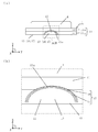
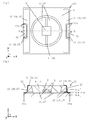
- FIG. 1A is a top view which shows the electronic device in the 1st Embodiment of this invention
- (b) is a bottom view of (a).
- (A) is a side view in the A direction of FIG. 1 (a)
- (b) is a principal part enlarged side view in the A section of (a).
- FIG. 2A is a cross-sectional view taken along line AA of the electronic device shown in FIG. 1A
- FIG. (A) And (b) is a principal part expanded sectional view in the other example of the electronic device in the 1st Embodiment of this invention, respectively.
- (A)-(d) is sectional drawing which shows the manufacturing method of the wiring board in the 1st Embodiment of this invention, respectively.
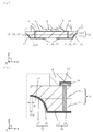
- FIG. 7A is a cross-sectional view taken along line AA of the electronic device shown in FIG. 7A
- FIG. 8 is an enlarged cross-sectional view of a main part showing an electronic module in which the electronic device in FIG. 7 is mounted on a module substrate.
- FIG. 12 is a cross-sectional view taken along line AA of the electronic device shown in FIG. (A) is a top view which shows the electronic device in the 4th Embodiment of this invention, (b) is sectional drawing in the AA of (a). It is a bottom view which shows the electronic device in the 5th Embodiment of this invention.
- the electronic device according to the first embodiment of the present invention includes a wiring board 1 and an electronic component 2 provided on the upper surface of the wiring board 1. As shown in the example shown in FIG. 6, the electronic device is connected to the module substrate 5 including the external circuit substrate 5 a by using solder 6, for example, when an electronic module is configured.
- the wiring substrate 1 includes an insulating base 11 having a notch 12 opened on the main surface and side surfaces, and an external circuit board 5a included in the module substrate 5 provided on the inner surface of the notch 12 with solder 6 And an inner surface electrode 13 connected to each other.
- the inner surface electrode 13 has nickel and gold on the surface side, the surface of the outer edge portion 13a has more nickel than gold, and the surface of the inner region has more gold than nickel.
- the electronic device is mounted on an xy plane in a virtual xyz space.
- the upward direction means the positive direction of the virtual z-axis.
- the insulating base 11 is composed of a single layer or a plurality of layers of insulating layers 11a, and has an upper surface including a mounting area of the electronic component 2, and has a rectangular plate shape when viewed from above, that is, from an upper direction perpendicular to the upper surface. It has the shape of The insulating base 11 functions as a support for supporting the electronic component 2, and the electronic component 2 is bonded and fixed to the mounting area in the center of the upper surface via a bonding member such as a low melting point brazing material or a conductive resin.
- a bonding member such as a low melting point brazing material or a conductive resin.
- the insulating substrate 11 may be made of ceramics such as an aluminum oxide sintered body (alumina ceramic), an aluminum nitride sintered body, a mullite sintered body, or a glass ceramic sintered body.
- alumina ceramic aluminum oxide sintered body
- aluminum nitride sintered body aluminum nitride sintered body
- mullite sintered body a glass ceramic sintered body
- the insulating substrate 11 is made of, for example, an aluminum oxide sintered body, a suitable organic binder and solvent are added to and mixed with raw material powders such as aluminum oxide, silicon oxide, magnesium oxide and calcium oxide to form a slurry. Then, this is formed into a sheet shape by the doctor blade method or the calender roll method to obtain a ceramic green sheet. After that, the ceramic green sheet is subjected to appropriate punching processing, and a plurality of these are laminated to obtain a high temperature (about 1600 Manufactured by baking at a temperature of ° C.
- a suitable organic binder and solvent are added to and mixed with raw material powders such as aluminum oxide, silicon oxide, magnesium oxide and calcium oxide to form a slurry. Then, this is formed into a sheet shape by the doctor blade method or the calender roll method to obtain a ceramic green sheet. After that, the ceramic green sheet is subjected to appropriate punching processing, and a plurality of these are laminated to obtain a high temperature (about 1600 Manufacture
- the notch 12 is open on the main surface and side surface of the insulating base 11. 1 to 3 and FIG. 6, the notch 12 opens in two directions, ie, the lower main surface (lower surface) and the side surface of the insulating base 11.
- the notch 12 may be opened in three directions of the upper main surface (upper surface), the lower main surface (lower surface), and the side surface of the insulating substrate 11.
- the notch 12 is formed in a semi-elliptical shape in plan view, and has a shape obtained by dividing the ellipsoid, that is, the inner surface is formed in a curved shape.
- the cut-out portion 12 may have a shape obtained by dividing a semispherical shape or a semi-elliptical shape in a plan view.
- a notch 12 is provided by forming a hole to be the notch 12 in the insulating base 11 by blasting or the like.
- the inner surface of the notch 12 is formed in a curved surface shape.
- the notch 12 is a columnar shape or a truncated frustum formed in a rectangular shape with an arcuate corner in a plan view, or a semicircular shape, a semi-elliptical shape or a semi-oval shape in a plan view, Alternatively, a columnar shape in which a plurality of cutout portions 12 having a plurality of sizes overlap each other or a shape obtained by dividing a frustum may be used.
- Such notches 12 are formed by forming through holes to be the notches 12 in some of the ceramic green sheets for the insulating substrate 11 by laser machining or punching with a mold.
- the inner surface electrode 13 is provided on the inner surface of the notch 12, and the wiring conductor 14 is provided on the surface and inside of the insulating base 11.
- the inner surface electrode 13 is provided on the entire inner surface of the notch 12.
- a main surface electrode 15 connected to the inner surface electrode 13 is provided on the main surface where the notch 12 is open.
- a configuration including the inner surface electrode 13 and the main surface electrode 15 serves as an outer electrode.
- the wiring conductor 14 and the main surface electrode 15 are connected on the lower surface of the insulating base 11.
- the inner surface electrode 13 and the wiring conductor 14 are electrically connected via the main surface electrode 15.
- External electrodes including the inner surface electrode 13 and the main surface electrode 15 are for bonding the wiring substrate 1 to the module substrate 5 including the external circuit substrate 5a.
- the inner surface electrode 13, the wiring conductor 14, and the main surface electrode 15 are for electrically connecting the electronic component 2 mounted on the wiring substrate 1 and the module substrate 5.
- the wiring conductor 14 includes a wiring conductor provided on the surface or inside of the insulating base 11, and a through conductor that electrically connects the wiring conductors that are positioned vertically through the insulating layer 11a constituting the insulating base 11. Contains.
- the inner surface electrode 13 or the main surface electrode 15 includes a thin film layer 16 and a plating layer 17.
- the thin film layer 16 includes, for example, an adhesion metal layer and a barrier layer.
- the adhesion metal layer constituting the thin film layer 16 is formed on the main surface of the insulating base 11 and the inner surface of the notch 12.
- the adhesion metal layer is made of, for example, tantalum nitride, nickel-chromium, nickel-chromium-silicon, tungsten-silicon, molybdenum-silicon, tungsten, molybdenum, titanium, chromium, or the like, such as vapor deposition, ion plating, or sputtering.
- the insulating substrate 11 is installed in a film forming chamber of a vacuum vapor deposition apparatus, a metal piece serving as an adhesion metal layer is disposed in a vapor deposition source in the film forming chamber, and then the formation is performed.
- the inside of the film chamber is evacuated (pressure of 10 ⁇ 2 Pa or less), the metal piece disposed in the vapor deposition source is heated and evaporated, and the molecules of the evaporated metal piece are deposited on the insulating substrate 11. Then, a thin film metal layer to be an adhesion metal layer is formed.
- an extra thin film metal layer is removed by etching to form an adhesion metal layer.
- a barrier layer is deposited on the top surface of the adhesion metal layer. The barrier layer has good bondability and wettability with the adhesion metal layer and the plating layer, and has a function of firmly bonding the adhesion metal layer and the plating layer and preventing mutual diffusion between the adhesion metal layer and the plating layer.
- the barrier layer is made of, for example, nickel-chromium, platinum, palladium, nickel, or cobalt, and is deposited on the surface of the adhesion metal layer by a thin film forming technique such as vapor deposition, ion plating, or sputtering.
- the thickness of the adhesion metal layer is preferably about 0.01 to 0.5 ⁇ m. If the thickness is less than 0.01 ⁇ m, it tends to be difficult to firmly adhere the adhesion metal layer on the insulating substrate 11. When the thickness exceeds 0.5 ⁇ m, peeling of the adhesion metal layer is likely to occur due to internal stress during the formation of the adhesion metal layer.
- the thickness of the barrier layer is preferably about 0.05 to 1 ⁇ m. When the thickness is less than 0.05 ⁇ m, defects such as pinholes are generated in the barrier layer, which tends to make it difficult to function as a barrier layer. When the thickness exceeds 1 ⁇ m, peeling of the barrier layer is likely to occur due to internal stress during film formation.
- the plating layer 17 is deposited on the surface of the thin film layer 16 by electroplating or electroless plating.
- the plating layer 17 is made of a metal having excellent corrosion resistance such as nickel, copper, gold, or silver and connectivity with the connection member.
- the nickel plating layer has a thickness of about 0.5 to 5 ⁇ m and a thickness of about 0.1 to 3 ⁇ m.
- the gold plating layers are sequentially deposited. Thus, corrosion of the inner surface electrode 13 and the main surface electrode 15 can be effectively suppressed, and the bonding between the inner surface electrode 13 and the main surface electrode 15 and the connection pad 51 for connection formed on the module substrate 5 can be strengthened. Can be.
- the wiring conductor 14 can be made of a metal material such as tungsten (W), molybdenum (Mo), manganese (Mn), silver (Ag), or copper (Cu).
- a metal material such as tungsten (W), molybdenum (Mo), manganese (Mn), silver (Ag), or copper (Cu).
- W tungsten
- Mo molybdenum
- Mn manganese
- Ag silver
- Cu copper
- a conductive paste obtained by adding and mixing a suitable organic binder and solvent to a refractory metal powder such as W, Mo or Mn is insulated.
- the wiring conductor 14 is attached to a predetermined position of the insulating base 11 by printing and applying in a predetermined pattern to the ceramic green sheet to be the base 11 in advance by a screen printing method and firing simultaneously with the ceramic green sheet to be the insulating base 11. It is formed.
- a through hole is formed in the green sheet by punching by a die or punching or laser processing, and a conductive paste for the wiring conductor 14 is filled into the through hole by a printing method. It is formed by placing.
- the exposed surface of the wiring conductor 14 is coated with a plating layer 17 by an electroplating method or an electroless plating method, similarly to the thin film layer 16 of the inner surface electrode 13 and the thin film layer 16 of the main surface electrode 15.
- the plating layer 17 is made of a metal having excellent corrosion resistance such as nickel, copper, gold, or silver and connectivity with the connection member.
- the nickel plating layer has a thickness of about 0.5 to 5 ⁇ m and a thickness of about 0.1 to 3 ⁇ m.
- a nickel plating layer having a thickness of about 1 to 10 ⁇ m and a silver plating layer having a thickness of about 0.1 to 1 ⁇ m are sequentially deposited.
- the inner surface electrode 13 has nickel and gold on the surface side, the surface of the outer edge portion 13a has more nickel than gold, and the surface of the inner region has more gold than nickel.
- the outer edge portion 13 a of the inner surface electrode 13 refers to the outer edge portion of the inner surface electrode 13 on the side surface side of the insulating base 11.
- the surface of the outer edge portion of the inner surface electrode 13 contains 50% or more of nickel
- the surface of the inner region of the inner surface electrode 13 contains 50% or more of gold.
- the nickel or gold content on the surface of the outer edge portion of the inner surface electrode 13 and the surface of the inner region, or the distribution state on the surface may be measured using an electron beam microanalyzer. In the example shown in FIGS.
- the outer edge portion 13 a of the inner surface electrode 13 is formed on the outer edge portion of the inner surface electrode 13 on the side surface side of the insulating substrate 11 along the opening of the notch portion 12 on the side surface side of the insulating substrate 11.
- the outer edge portion 13a of the inner surface electrode 13 is indicated by hatching in FIGS.
- the width W of the outer edge portion 13a of the inner surface electrode 13 is excellent in electrical connection reliability with the module substrate 5 including the external circuit substrate 5a over a long period of time when formed to a width of about 0.01 mm ⁇ W ⁇ 0.2 mm. A small and highly accurate wiring board 1 can be obtained.
- the outer edge portion 13a of the inner surface electrode 13 can be formed by partially applying heat to the outer edge portion of the inner surface electrode 13 on the side surface side of the insulating base 11. For example, heat is applied to the outer edge portion on the side surface side of the insulating base 11 in the inner surface electrode 13 including the thin film layer 16 and the plating layer 17 so as not to remove the inner surface electrode 13 by laser irradiation, thereby insulating the inner surface electrode 13. What is necessary is just to change the outer edge part of the side surface side of the base 11.
- the plating layer 17 of the inner surface electrode 13 is composed of two layers of a Ni plating layer and an Au plating layer, heat is applied to the outer edge portion of the inner surface electrode 13 on the side surface side of the insulating substrate 11 by laser irradiation.
- Ni in the Ni plating layer is diffused into the Au plating layer and deposited on the surface of the Au plating layer, that is, the surface of the plating layer 17 has a component (Ni) that is difficult to wet with the solder 6.
- the outer edge portion 13a of the inner surface electrode 13 can be formed with a portion that is difficult to wet with the solder 6, and the inner surface of the inner surface electrode 13 and the main surface electrode 15 are easily wetted with the solder 6 by suppressing the application of heat. It can be in a state.
- the inner region surface of the inner surface electrode 13 has more gold than nickel, so that no heat is applied to the inner region of the inner surface electrode 13 by laser irradiation. Including that the surface of the region is substantially free of nickel.
- the outer edge portion 13a of the inner surface electrode 13 is a component that easily wets the solder 6 on the surface (Au) when the plating layer 17 of the inner surface electrode 13 is composed of two layers of the Ni plating layer and the Au plating layer as described above. ),
- the surface of the outer edge portion 13a of the inner surface electrode 13 can be effectively prevented from getting wet with the solder 6, so that the wiring board 1 and It is possible to effectively suppress the stress due to the difference in thermal expansion with the module substrate 5 from being applied to the outer edge portion 13a of the inner surface electrode 13 via the solder 6, and to reduce the possibility that the inner surface electrode 13 is peeled off from the insulating substrate 11. it can.
- the solder 6 tends to get wet. This can be confirmed by measuring the components and components that are difficult to wet with solder and the distribution.
- the outer edge portion 13a of the inner surface electrode 13 may be provided away from the opening of the notch portion 12 on the side surface side of the insulating base 11, but when the inner edge electrode 13 is provided along the opening of the notch portion 12, the inner surface Since the outer edge portion 13a of the electrode 13a is not easily wetted and the inner region of the inner surface electrode 13a can be widened, the connection pads 51 formed on the inner surface electrode 13 and the main surface electrode 15 and the module substrate 5 are provided. Thus, the wiring substrate 1 can be bonded well.
- the wiring board 1 includes an insulating base 11 having a notch 12 that opens in two directions, a main surface and a side surface, and an external circuit board 5 a provided on the inner surface of the notch 12 via a solder 6.
- the inner surface electrode 13 has nickel and gold on the surface side, and the surface of the outer edge portion 13a has more nickel than gold. Since the surface of the region has more gold than nickel, the formation of the solder 6 on the outer edge portion 13a of the inner surface electrode 13 is suppressed.
- the wiring conductor 14 and the main surface electrode 15 are connected to the main surface (lower surface) of the insulating base 11.
- the inner surface electrode 13 and the wiring conductor 14 are formed on the inner surface portion of the notch portion 12 on the opposite side of the inner surface electrode 13 from the main surface (lower surface) of the insulating base 11.
- the wiring conductor 14 and the main surface electrode 15 are connected via the inner surface electrode 13.
- the inner surface electrode 13 and the wiring conductor 14 are connected at the inner surface of the notch 12, and the wiring conductor 14 and the main surface electrode 15 are connected from the inner surface of the notch 12 to the inner surface.
- the electrodes 13 and the main surface (lower surface) of the insulating base 11 are directly connected to each other.
- the wiring conductor 14 is connected to the main surface electrode 15, the main surface electrode 15 is firmly adhered to the main surface of the insulating base 11, so that the inner surface electrode 13 and the wiring conductor are formed on the inner surface of the notch 12.
- the electrical connection between the wiring board 1 on which the electronic component 2 is mounted and the module board 5 including the external circuit board 5a can be improved.
- the wiring board 1 according to the first embodiment of the present invention can be manufactured, for example, by the following manufacturing method.
- an insulating mother substrate 111 made of a plurality of insulating layers 111a having a wiring conductor 14 formed inside and on the surface is prepared.
- the insulating mother substrate 111 has a shape in which a plurality of insulating bases 11 are connected, for example, the shape of a multi-cavity wiring substrate, and a hemispherical concave portion 112 that becomes a notch portion 12 opened in the lower main surface. have.
- Such a recess 112 is formed by using, for example, blasting as described above.
- the inner electrode 13 including the thin film layer 16 and the plating layer 17 is formed on the inner surface of the recess 112 that becomes the notch 12 of the insulating mother substrate 111. Then, the main surface electrode 15 including the thin film layer 16 and the plating layer 17 is formed on the surface of the insulating mother substrate 111.
- heat is applied to a predetermined region of the inner surface electrode 13 on the inner surface of the recess 112 by laser irradiation, and the inner surface electrode 13 is formed along the outer edge serving as the wiring substrate 1.
- a portion (a portion including gold and nickel) that is difficult to wet with the solder 6 is formed on the surface.
- the surface of the outer edge portion 13a has more nickel than gold by dividing the concave portion 112 by using a slicing method or the like.
- the wiring board 1 having the inner electrode 13 whose surface has more gold than nickel can be manufactured.
- the inner surface electrode 13 and the inner surface electrode are formed on the inner surface of the recess 112. Thirteen outer edge portions 13a (portions that are difficult to wet with solder 6) can be easily formed.
- the portion that is difficult to get wet with the solder 6 formed on the surface is larger than the blade width when the recess 112 is divided by the slicing method. If it is formed so as to be 110% or more of the blade width, the surface of the outer edge portion 13a of the inner surface electrode 13 along the edge of the opening has more nickel than gold and is difficult to wet the solder 6, and the inner region Thus, the wiring board 1 having a larger amount of gold than nickel and easily wetted by the solder 6 can be manufactured satisfactorily.
- the inner surface electrode 13 formed on the inner surface of the recess 112 is provided with a portion that is difficult to wet with the plurality of rows of solder 6, and the surface of the plurality of rows including the outer edge portion 13 a of the inner surface electrode 13 is divided.
- a wiring board 1 that has more nickel than gold and hardly wets the solder 6, and the surface excluding the plurality of rows in the inner region has more gold than nickel and easily wets the solder 6 may be manufactured. Absent.
- the recess 112 is divided so that the surfaces shown in FIGS. Even if the thin film layer 16 and the plating layer 17 of the inner surface electrode 13 are exposed on the side surface of the insulating substrate 11, it is possible to prevent the thin film layer 16 and the plating layer 17 from flowing to the exposed end portion of the thin film layer 16 of the inner surface electrode 13.
- the concave portion 112 inside the insulating mother substrate 111 is viewed in plan view.
- the wiring conductor 14 is formed in the overlapping region, and after exposing the wiring conductor 14 to the inside of the recess 112 by blasting or the like, the inner surface electrode 13 is formed on the inner surface of the recess 112, and the inner surface electrode 13 and the wiring conductor 14 Can be connected.
- heat may be applied to the outer edge portion 13a of the inner surface electrode 13 provided on the inner surface of the notch portion 12 by laser irradiation so that the solder 6 is hardly wetted.
- the outer edge portion 13a of the inner surface electrode 13 can be irradiated by laser irradiation from the side surface direction of the insulating base 11 after the division, the surface of the outer edge portion 13a is made to be more than the gold when the notch portion 12 is small. It is easy to form the inner electrode 13 having a large amount of nickel and difficult to get wet with the solder 6 with high accuracy, and the wiring board 1 having a good electrical connection between the smaller electronic component 2 and the wiring board 1 and module board 5. Can be produced.
- An electronic device can be manufactured by mounting the electronic component 2 on the upper surface of the wiring board 1.
- the electronic component 2 mounted on the wiring board 1 is a semiconductor element such as an IC chip or an LSI chip, a light emitting element, a piezoelectric element such as a crystal vibrator or a piezoelectric vibrator, and various sensors.
- the semiconductor element is fixed onto the wiring conductor 14 by a bonding member such as a low melting point brazing material or a conductive resin, and then bonded to a bonding wire or the like.
- the electrode of the semiconductor element and the wiring conductor 14 are electrically connected via the connecting member 3 to be mounted on the wiring board 1.
- the semiconductor element 2 is a flip-chip type semiconductor element
- the semiconductor element is connected via a connecting member 3 such as a solder bump, a gold bump, or a conductive resin (anisotropic conductive resin, etc.)
- the electrode of the semiconductor element and the wiring conductor 14 are mounted on the wiring board 1 by being electrically and mechanically connected.
- a plurality of electronic components 2 may be mounted on the wiring board 1, or small electronic components such as a resistance element and a capacitive element may be mounted as necessary.
- the electronic component 2 is sealed with a sealing material 4 made of resin, glass, or the like, a lid made of resin, glass, ceramics, metal, or the like, as necessary.
- the electronic device of the present embodiment is connected to the connection pads 51 of the module substrate 5 including the external circuit substrate 5a via the solder 6 as in the example shown in FIG.
- the solder 6 is joined to the inner surface electrode 13 in the notch 12 and to the main surface electrode 17 on the lower surface of the insulating base 11. Further, the solder 6 is inclined so as to spread from the inner end of the inner surface electrode 13 excluding the outer edge portion 13a of the inner surface electrode 13 to the outer end of the connection pad 51, and the surface has more nickel than gold.
- the outer edge portion 13 a of the inner surface electrode 13 having the solder 6 prevents the solder 6 from being formed on the outer edge portion 13 a of the inner surface electrode 13.
- the solder 6 is applied to the insulating base 11 having the notch 12 opened on the main surface and the side surface, and the external circuit board 5a provided on the inner surface of the notch 12.
- the inner surface electrode 13 has nickel and gold on the surface side, and the surface of the outer edge portion 13a has more nickel than gold, Since the surface of the inner region has more gold than nickel, the formation of the solder 6 on the outer edge portion 13a of the inner surface electrode 13 is suppressed, and the thermal expansion between the wiring board 1 and the external circuit board 5a.
- the wiring board 1 in the present embodiment can be suitably used in a small and high-power electronic device, and electrical connection in the wiring board 1 can be favorably achieved.
- the electronic component 2 can be suitably used as a small-sized wiring board 1 for mounting a light emitting element on which a high light emitting element is mounted.
- the notched portion 12 having the bottom when the notched portion 12 having the bottom can be formed, it can be formed from a single insulating layer 11a. 1 can be formed.
- the inner surface of the notch 12 is curved, it is easy to irradiate a laser to a portion that becomes the outer edge 13a of the inner electrode 13 of the notch 12, and the outer edge 13a of the inner electrode 13 on the inner surface of the notch 12
- a highly accurate wiring board 1 can be obtained.
- the electrical reliability is improved by having the wiring board 1 having the above-described configuration.
- the electronic module according to another aspect of the present invention includes the module substrate 5 having the connection pads 51 on the main surface, and the electronic device having the above configuration in which the inner surface electrode 13 is connected to the connection pads 51 via the solder 6. Therefore, the electrical connection reliability between the wiring substrate 1 and the module substrate 5 can be excellent over a long period of time.
- the electronic device according to the second embodiment of the present invention is different from the electronic device according to the first embodiment described above in that, as in the examples shown in FIGS.
- the corner portion is formed in an arc-shaped rectangular shape, and is a shape obtained by dividing a rectangular frustum formed long along the outer side of the insulating base 11, and the main surface electrode 15 is formed on the insulating base 11. It is a point provided on the upper surface.
- the formation of the solder 6 on the outer edge portion 13a of the inner surface electrode 13 is suppressed, and the wiring board 1 and the external circuit board are suppressed. It is possible to suppress the stress due to the difference in thermal expansion with respect to 5a from being applied to the outer edge portion 13a of the inner surface electrode 13 via the solder 6, and to reduce the possibility that the inner surface electrode 13 is peeled off from the insulating substrate 11, and for a long period of time. A small and highly accurate wiring board 1 having excellent electrical connection reliability with the external circuit board 5a can be obtained.
- the main surface electrode 15 provided on the upper surface of the insulating substrate 11 is used as wiring for mounting the electronic component 2 or connecting the connecting member 3. Since the main surface electrode 15 is provided on the upper surface of the insulating base 11, the electronic component 2 can be mounted on the wiring board 1 with high accuracy. For example, when a light-emitting element is mounted as the electronic component 2, a light-emitting device that can emit light with high accuracy can be obtained by mounting with high accuracy.
- the notch 12 may have a shape obtained by dividing the columnar shape, but, as in the examples shown in FIGS. 7 to 9, the opening on the lower surface side of the insulating base 11 with respect to the width of the bottom of the notch 12 is used. If the quadrangular pyramid shape having a large width is divided, the inner surface electrode 13 and the outer edge portion 13a of the inner surface electrode 13 on the inner surface of the notch portion 12 can be satisfactorily formed.
- the notch 12 in the wiring substrate 1 according to the second embodiment is formed on some of the ceramic green sheets for the insulating base 11 by laser machining, die cutting, or the like. It is formed by forming a through hole.
- the wiring substrate is excellent in reliability of electrical connection with the module substrate 5. 1 can be used.
- the wiring board 1 of the second embodiment can be manufactured using the same method as that of the first embodiment except for the method of forming the notch 12.
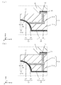
- the electronic device according to the third embodiment of the present invention is different from the electronic device according to the first embodiment described above in that a cavity 18 is formed on the upper surface of the insulating substrate 11 as in the example shown in FIGS. It is a point.
- the formation of the solder 6 on the outer edge portion of the inner surface electrode 13 is suppressed, and the wiring board 1 and the external circuit board 5a are suppressed. It is possible to suppress the stress due to the difference in thermal expansion between the inner electrode 13 and the outer edge portion 13a of the inner surface electrode 13 through the solder 6, and to reduce the possibility that the inner surface electrode 13 is peeled off from the insulating base 11, and for a long period of time. A small and highly accurate wiring board 1 having excellent electrical connection reliability with the circuit board 5a can be obtained.
- the depth of the notch 12 having a shape obtained by dividing a semi-spherical hemisphere in plan view is the cavity. If the height (depth) of the bottom surface of 18 is not reached, the strength of the insulating base 11 can be made difficult to decrease, and the notch 12 can be satisfactorily formed on the bottom surface of the insulating base 11. be able to.
- the insulating substrate 11 has an upper surface including a cavity 18 as in the example shown in FIGS.
- Such cavities 18 are formed by forming through holes in the ceramic green sheets into a plurality of ceramic green sheets by laser processing or punching with a mold, and forming these through holes. It can be formed by laminating the ceramic green sheets.
- the through hole for the cavity 18 is formed by laser processing or punching with a mold after the ceramic green sheets are laminated, because it can be processed with high accuracy.
- the width of the notch 12 is about 25% to 75% of the width of the side wall of the cavity 18.
- the angle ⁇ formed between the inner surface of the cavity 18 and the bottom surface of the cavity 18 is an obtuse angle, and may be 110 ° to 145 °.
- the angle ⁇ is in such a range, it is easy to stably and efficiently form the inner surface of the through-hole serving as the cavity 18 by punching, and the light emitting device using the wiring board 1 can be easily downsized.
- the light emitted from the light emitting element can be emitted well toward the outside.
- the cavity 18 having such an inner surface of the angle ⁇ is formed by punching the ceramic green sheet using a punching die in which the clearance between the punch diameter and the die hole diameter is set large.
- the green sheet is punched when the ceramic green sheet is punched from the main surface side to the other main surface side. Is formed so that the diameter of the through hole spreads from the main surface side to the other main surface side by shearing from the edge of the contact surface to the edge of the contact surface with the die hole.
- the angle of the inner surface of the through hole formed in the ceramic green sheet can be adjusted by setting the clearance between the diameter of the punch and the diameter of the die hole according to the thickness of the ceramic green sheet.
- Such a punching method is high in productivity because the angle ⁇ formed by the inner surface of the cavity 18 and the bottom surface of the cavity 18 can be set to a desired angle only by punching.
- a truncated cone shape or a truncated pyramid shape is formed on the inner surface of the through hole.
- a through-hole having an angle ⁇ extending from one main surface side to the other main surface side as described above may be formed by pressing the mold. In such a case, the angle ⁇ formed by the inner surface of the cavity 18 and the bottom surface of the cavity 18 can be adjusted with higher accuracy.
- the wiring substrate 1 has an insulating base 11 having an upper surface including the cavity 18 on which the light emitting element is mounted, for example, a reflection layer for reflecting light emitted from the light emitting element is provided on the inner wall surface of the cavity 18. It may be done.
- the reflective layer has, for example, a metal conductor layer provided on the inner wall surface of the cavity 18 and a plating layer deposited on the metal conductor layer.
- the metal conductor layer can be formed by the same material and method as those for the inner surface electrode 13 and the wiring conductor 14 or the main surface electrode 15.
- a silver plating layer is deposited on the outermost surface of the metal conductor layer, and gold plating is applied on the outermost surfaces of the inner surface electrode 13, the wiring conductor 14, and the main surface electrode 15. It is preferred to deposit the layer.
- the gold plating layer is superior in bondability with the electronic component 2, the connection member 3, and the solder 6 as compared with the silver plating layer, and the silver plating layer has a higher reflectance to light than the gold plating layer.
- the outermost surface of the wiring and the metal conductor layer where the light emitting element is mounted may be an alloy plating layer of silver and gold, for example, an alloy plating layer that is a solid solution of silver and gold.
- the wiring board 1 of the third embodiment can be suitably used in a small and high-power electronic device, and electrical connection in the wiring board 1 can be favorably achieved.
- the electronic component 2 can be suitably used as a small wiring board for mounting a light emitting element on which a high light emitting element is mounted.
- the wiring board 1 of the third embodiment can be manufactured using the same manufacturing method as that of the first embodiment.
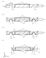
- the electronic device according to the fourth embodiment of the present invention differs from the electronic device according to the first embodiment described above in that the notch portion 12 is different from the mounting surface of the electronic component 2 as in the example shown in FIG. It is the point which opens to the same one main surface (henceforth an upper surface) and a side surface.
- the formation of the solder 6 on the outer edge portion 13a of the inner surface electrode 13 is suppressed. It is possible to suppress the stress due to the difference in thermal expansion with the external circuit board 5a from being applied to the outer edge portion 13a of the inner surface electrode 13 via the solder 6, and to reduce the possibility that the inner surface electrode 13 is peeled off from the insulating substrate 11. A small and highly accurate wiring board having excellent electrical connection reliability with the external circuit board 5a over a long period of time can be obtained.
- a wiring board 1 can be joined to the module board 5 with the solder 6 on the upper surface side of the wiring board 1, a member having a higher thermal conductivity than the insulating substrate 11 is joined to the entire lower surface side of the wiring board 1.
- the heat dissipation of the wiring board 1 can be improved.
- a material having higher thermal conductivity than the insulating substrate 11 when the insulating substrate 11 is made of an aluminum oxide sintered body, a metal such as copper (Cu), copper-tungsten (Cu-W), or aluminum (Al) is used. Examples thereof include an insulator made of a material and an aluminum nitride sintered body.
- the wiring board 1 In such a wiring board 1, the amount of heat transferred from the electronic component 2 mounted on the wiring board 1 to the notch 12 side is suppressed, and the wiring is excellent in electrical connection reliability and heat dissipation with the module board 5 over a long period of time. It can be a substrate.
- the wiring board 1 of the fourth embodiment can be suitably used in a small and high-power electronic device, and electrical connection in the wiring board 1 can be favorably achieved.
- the electronic component 2 can be suitably used as a small wiring board for mounting a light emitting element on which a high light emitting element is mounted.
- the wiring board 1 of the fourth embodiment can be manufactured using the same manufacturing method as that of the second embodiment.
- the electronic device according to the fifth embodiment of the present invention is different from the electronic device according to the first embodiment described above in that the surface of the outer edge portion 15a of the main surface electrode 15 is made of gold as in the example shown in FIG. It is a point which has more nickel than the solder 6 and is hard to get wet.
- the solder 6 is suppressed from being formed on the outer edge portion 15a of the main surface electrode 15, and the wiring board 1 and the module board 5 including the external circuit board 5a are connected.
- the stress due to the difference in thermal expansion can be suppressed from being applied to the outer edge portion 15a of the main surface electrode 15 via the solder 6, and the possibility that the main surface electrode 15 is peeled off from the insulating base 11 can be reduced.
- the wiring board can be made.
- the reason why the surface of the outer edge portion 15a of the main surface electrode 15 has more nickel than gold and is difficult to wet the solder 6 is that the surface of the outer edge portion 13a of the inner surface electrode 13 has more nickel than gold. It can be formed by using a method similar to that for preventing the solder 6 from getting wet.
- the wiring board 1 of the fifth embodiment can be manufactured using the same manufacturing method as that of the first embodiment.
- the present invention is not limited to the above-described embodiments, and various modifications can be made.
- the notch portion 12 and the inner surface electrode 13 are each provided on the two opposing side surfaces of the insulating base 11, but the notch portion 12 and the inner surface electrode 13 are provided on the insulating base 11.
- the wiring board 1 provided on all four side surfaces, or the wiring board 1 provided with the plurality of notches 12 and the inner surface electrode 13 on each side may be used.
- the insulating base 11 is formed of two or three insulating layers 11a.
- the insulating substrate 11 may be formed of a single layer or four or more insulating layers 11a. I do not care.
- the notch 12 is opened on one main surface and side surface of the insulating base 11, but may be opened on both main surface and side surface of the insulating base 11. Absent.
- the wiring board 1 may have an electronic component mounting layer 19 and a central terminal layer 20 which are conductors other than the wiring.
- these conductors include, for example, the thin film layer 16 and the plating layer 17, they can be manufactured by the same material and method as the inner surface electrode 13 and the main surface electrode 15 described above.
- the metal plating layer 17 is provided on the exposed surface.
- the electronic component mounting layer 19 is used, for example, for mounting the electronic component 2
- the central terminal layer 20 is used, for example, for bonding to the module substrate 5 similarly to the inner surface electrode 13 and the main surface electrode 15.
- the central terminal layer 20 may also be connected to the inner surface electrode 13 provided on the inner surface of the notch portion 12.
- each of the wiring boards 1 in the first to fifth embodiments may be a flat wiring board 1 or a wiring board 1 having a cavity 18. Further, the wiring board 1 in the first to fifth embodiments may include the electronic component mounting layer 19 and the central terminal layer 20.
- one electronic component 2 is mounted on the wiring board 1, but it may be a wiring board 1 on which a plurality of electronic components 2 are mounted. It may be manufactured in the form of a single-piece wiring board.
Landscapes
- Engineering & Computer Science (AREA)
- Microelectronics & Electronic Packaging (AREA)
- Printing Elements For Providing Electric Connections Between Printed Circuits (AREA)
- Electric Connection Of Electric Components To Printed Circuits (AREA)
- Structure Of Printed Boards (AREA)
- Physics & Mathematics (AREA)
- Geometry (AREA)
Abstract
Description
本発明の第1の実施形態における電子装置は、図1~図3および図6に示すように、配線基板1と、配線基板1の上面に設けられた電子部品2とを含んでいる。電子装置は、図6に示す例のように、例えば電子モジュールを構成する場合には、外部回路基板5aを含むモジュール基板5上にはんだ6を用いて接続される。
次に、本発明の第2の実施形態による電子装置について、図7~図10を参照しつつ説明する。
次に、本発明の第3の実施形態による電子装置について、図11および図12を参照しつつ説明する。
次に、本発明の第4の実施形態による電子装置について、図13を参照しつつ説明する。
次に、本発明の第5の実施形態による電子装置について、図14を参照しつつ説明する。
また、配線基板1は多数個取り配線基板の形態で製作されていてもよい。
11・・・・絶縁基体
11a・・・絶縁層
12・・・・切欠き部
13・・・・内面電極
13a・・・内面電極の外縁部
14・・・・配線導体
15・・・・主面電極
16・・・・薄膜層
17・・・・めっき層
18・・・・キャビティ
19・・・・電子部品搭載層
20・・・・中央端子層
2・・・・電子部品
3・・・・接続部材
4・・・・封止材
5・・・・モジュール基板
5a・・・外部回路基板
51・・・・接続パッド
6・・・・はんだ
Claims (6)
- 主面および側面に開口する切欠き部を有している絶縁基体と、
前記切欠き部の内面に設けられた、外部回路基板にはんだを介して接続される内面電極とを有しており、
該内面電極は、表面側にニッケルおよび金を有しているとともに、外縁部の表面が金よりもニッケルを多く有しており、内側の領域の表面がニッケルよりも金を多く有していることを特徴とする配線基板。 - 前記外縁部は、前記側面側の前記切欠き部の開口に沿って設けられていることを特徴とする請求項1に記載の配線基板。
- 前記切欠き部は、内面が曲面状であることを特徴とする請求項1または請求項2に記載の配線基板。
- 前記切欠き部は、底部の幅よりも前記主面側の開口の幅が大きい四角錐台形状を分割した形状であることを特徴とする請求項1または請求項2に記載の配線基板。
- 請求項1乃至請求項4のいずれかに記載の配線基板と、
該配線基板に搭載され、前記内面電極に電気的に接続された電子部品とを有することを特徴とする電子装置。 - 主面に接続パッドを有するモジュール基板と、
前記接続パッドにはんだを介して前記内面電極が接続された請求項5に記載の電子装置とを有することを特徴とする電子モジュール。
Priority Applications (4)
| Application Number | Priority Date | Filing Date | Title |
|---|---|---|---|
| CN201580031717.5A CN106463470B (zh) | 2014-07-29 | 2015-07-23 | 布线基板、电子装置以及电子模块 |
| EP15826384.8A EP3176818B1 (en) | 2014-07-29 | 2015-07-23 | Wiring board, electronic device, and electronic module |
| JP2016538307A JP6298163B2 (ja) | 2014-07-29 | 2015-07-23 | 配線基板、電子装置および電子モジュール |
| US15/322,217 US9852975B2 (en) | 2014-07-29 | 2015-07-23 | Wiring board, electronic device, and electronic module |
Applications Claiming Priority (2)
| Application Number | Priority Date | Filing Date | Title |
|---|---|---|---|
| JP2014-153951 | 2014-07-29 | ||
| JP2014153951 | 2014-07-29 |
Publications (1)
| Publication Number | Publication Date |
|---|---|
| WO2016017523A1 true WO2016017523A1 (ja) | 2016-02-04 |
Family
ID=55217424
Family Applications (1)
| Application Number | Title | Priority Date | Filing Date |
|---|---|---|---|
| PCT/JP2015/070971 Ceased WO2016017523A1 (ja) | 2014-07-29 | 2015-07-23 | 配線基板、電子装置および電子モジュール |
Country Status (5)
| Country | Link |
|---|---|
| US (1) | US9852975B2 (ja) |
| EP (1) | EP3176818B1 (ja) |
| JP (1) | JP6298163B2 (ja) |
| CN (1) | CN106463470B (ja) |
| WO (1) | WO2016017523A1 (ja) |
Cited By (1)
| Publication number | Priority date | Publication date | Assignee | Title |
|---|---|---|---|---|
| EP3633719A4 (en) * | 2017-05-26 | 2021-03-17 | Kyocera Corporation | SUBSTRATE FOR THE ASSEMBLY OF ELECTRONIC COMPONENTS, ELECTRONIC DEVICE AND ELECTRONIC MODULE |
Families Citing this family (12)
| Publication number | Priority date | Publication date | Assignee | Title |
|---|---|---|---|---|
| JP6770331B2 (ja) * | 2016-05-02 | 2020-10-14 | ローム株式会社 | 電子部品およびその製造方法 |
| JP6817858B2 (ja) * | 2017-03-17 | 2021-01-20 | 日本電波工業株式会社 | 表面実装型デバイス及びその製造方法 |
| US10062511B1 (en) * | 2017-06-08 | 2018-08-28 | Samsung Electro-Mechanics Co., Ltd. | Multilayer electronic component and board having the same |
| US11309251B2 (en) | 2017-07-31 | 2022-04-19 | AdTech Ceramics Company | Selective metallization of integrated circuit packages |
| US10615321B2 (en) * | 2017-08-21 | 2020-04-07 | Seoul Semiconductor Co., Ltd. | Light emitting device package |
| JP6755233B2 (ja) * | 2017-12-14 | 2020-09-16 | ミネベアミツミ株式会社 | 基板および面状照明装置 |
| CN110176442B (zh) * | 2019-05-30 | 2021-03-02 | 苏州浪潮智能科技有限公司 | 一种防桥接的芯片引脚 |
| US11837684B2 (en) * | 2019-11-21 | 2023-12-05 | Creeled, Inc. | Submount structures for light emitting diode packages |
| JP7242911B2 (ja) * | 2020-01-24 | 2023-03-20 | 京セラ株式会社 | 配線基体および電子装置 |
| JP2022125445A (ja) * | 2021-02-17 | 2022-08-29 | 三菱電機株式会社 | 半導体装置及びその製造方法 |
| EP4184572A1 (en) * | 2021-11-18 | 2023-05-24 | Nexperia B.V. | Substrate-based package semiconductor device with side wettable flanks |
| US20240304539A1 (en) * | 2023-03-10 | 2024-09-12 | Advanced Technical Ceramics Company | Metal-ceramic mixed package substrate plated with non-magnetic layer stack |
Citations (3)
| Publication number | Priority date | Publication date | Assignee | Title |
|---|---|---|---|---|
| JP2002158509A (ja) * | 2000-11-21 | 2002-05-31 | Mitsubishi Electric Corp | 高周波回路モジュールおよびその製造方法 |
| US20100133693A1 (en) * | 2008-12-03 | 2010-06-03 | Texas Instruments Incorporated | Semiconductor Package Leads Having Grooved Contact Areas |
| JP2011049260A (ja) * | 2009-08-25 | 2011-03-10 | Ngk Spark Plug Co Ltd | 回路基板に対するガスセンサ素子搭載パッケージの表面実装構造 |
Family Cites Families (9)
| Publication number | Priority date | Publication date | Assignee | Title |
|---|---|---|---|---|
| JP2006086453A (ja) * | 2004-09-17 | 2006-03-30 | Yamato Denki Kogyo Kk | 表面処理方法、および電子部品の製造方法 |
| JP2006303335A (ja) * | 2005-04-25 | 2006-11-02 | Sony Corp | 電子部品搭載用基板及びそれを用いた電子装置 |
| WO2009001621A1 (ja) * | 2007-06-26 | 2008-12-31 | Murata Manufacturing Co., Ltd. | 部品内蔵基板の製造方法 |
| CN102362430B (zh) * | 2009-04-03 | 2016-08-17 | 株式会社大真空 | 封装构件组件及其制造方法、封装构件以及使用了封装构件的压电振动器件的制造方法 |
| JP4612727B2 (ja) * | 2009-04-13 | 2011-01-12 | 住友電気工業株式会社 | リード線 |
| JP2011114019A (ja) * | 2009-11-24 | 2011-06-09 | Panasonic Electric Works Co Ltd | 回路モジュールおよび回路モジュールの実装方法 |
| JP5763962B2 (ja) * | 2011-04-19 | 2015-08-12 | 日本特殊陶業株式会社 | セラミック配線基板、多数個取りセラミック配線基板、およびその製造方法 |
| JP5734434B2 (ja) * | 2011-07-25 | 2015-06-17 | 京セラ株式会社 | 配線基板、電子装置および電子モジュール |
| JP2014127678A (ja) * | 2012-12-27 | 2014-07-07 | Kyocera Corp | 配線基板および電子装置 |
-
2015
- 2015-07-23 WO PCT/JP2015/070971 patent/WO2016017523A1/ja not_active Ceased
- 2015-07-23 US US15/322,217 patent/US9852975B2/en active Active
- 2015-07-23 EP EP15826384.8A patent/EP3176818B1/en active Active
- 2015-07-23 CN CN201580031717.5A patent/CN106463470B/zh not_active Expired - Fee Related
- 2015-07-23 JP JP2016538307A patent/JP6298163B2/ja active Active
Patent Citations (3)
| Publication number | Priority date | Publication date | Assignee | Title |
|---|---|---|---|---|
| JP2002158509A (ja) * | 2000-11-21 | 2002-05-31 | Mitsubishi Electric Corp | 高周波回路モジュールおよびその製造方法 |
| US20100133693A1 (en) * | 2008-12-03 | 2010-06-03 | Texas Instruments Incorporated | Semiconductor Package Leads Having Grooved Contact Areas |
| JP2011049260A (ja) * | 2009-08-25 | 2011-03-10 | Ngk Spark Plug Co Ltd | 回路基板に対するガスセンサ素子搭載パッケージの表面実装構造 |
Non-Patent Citations (1)
| Title |
|---|
| See also references of EP3176818A4 * |
Cited By (1)
| Publication number | Priority date | Publication date | Assignee | Title |
|---|---|---|---|---|
| EP3633719A4 (en) * | 2017-05-26 | 2021-03-17 | Kyocera Corporation | SUBSTRATE FOR THE ASSEMBLY OF ELECTRONIC COMPONENTS, ELECTRONIC DEVICE AND ELECTRONIC MODULE |
Also Published As
| Publication number | Publication date |
|---|---|
| EP3176818B1 (en) | 2019-09-04 |
| JP6298163B2 (ja) | 2018-03-20 |
| US9852975B2 (en) | 2017-12-26 |
| US20170148718A1 (en) | 2017-05-25 |
| CN106463470B (zh) | 2019-04-05 |
| EP3176818A4 (en) | 2018-05-02 |
| CN106463470A (zh) | 2017-02-22 |
| JPWO2016017523A1 (ja) | 2017-04-27 |
| EP3176818A1 (en) | 2017-06-07 |
Similar Documents
| Publication | Publication Date | Title |
|---|---|---|
| JP6298163B2 (ja) | 配線基板、電子装置および電子モジュール | |
| JP6267803B2 (ja) | 配線基板、電子装置および電子モジュール | |
| JP6133854B2 (ja) | 配線基板および電子装置 | |
| JP6194104B2 (ja) | 配線基板、電子装置および電子モジュール | |
| JP6140834B2 (ja) | 配線基板および電子装置 | |
| JP2014127678A (ja) | 配線基板および電子装置 | |
| JP6133901B2 (ja) | 配線基板、電子装置および発光装置 | |
| JP6306474B2 (ja) | 配線基板、電子装置および電子モジュール | |
| JP6325346B2 (ja) | 配線基板、電子装置および電子モジュール | |
| JP6374293B2 (ja) | 配線基板、電子装置および電子モジュール | |
| JP6271882B2 (ja) | 配線基板および電子装置 | |
| JP6166194B2 (ja) | 配線基板、電子装置および電子モジュール | |
| JP6224473B2 (ja) | 配線基板、電子装置および電子モジュール | |
| JP6267068B2 (ja) | 配線基板、電子装置および電子モジュール | |
| JP2017135281A (ja) | 電子部品搭載用パッケージ、電子装置および電子モジュール | |
| JP5631268B2 (ja) | 配線基板 | |
| CN115152040A (zh) | 电子元件安装用封装和电子设备 |
Legal Events
| Date | Code | Title | Description |
|---|---|---|---|
| 121 | Ep: the epo has been informed by wipo that ep was designated in this application |
Ref document number: 15826384 Country of ref document: EP Kind code of ref document: A1 |
|
| ENP | Entry into the national phase |
Ref document number: 2016538307 Country of ref document: JP Kind code of ref document: A |
|
| REEP | Request for entry into the european phase |
Ref document number: 2015826384 Country of ref document: EP |
|
| WWE | Wipo information: entry into national phase |
Ref document number: 15322217 Country of ref document: US |
|
| NENP | Non-entry into the national phase |
Ref country code: DE |