WO2016021491A1 - パワーモジュール用基板の製造方法 - Google Patents
パワーモジュール用基板の製造方法 Download PDFInfo
- Publication number
- WO2016021491A1 WO2016021491A1 PCT/JP2015/071776 JP2015071776W WO2016021491A1 WO 2016021491 A1 WO2016021491 A1 WO 2016021491A1 JP 2015071776 W JP2015071776 W JP 2015071776W WO 2016021491 A1 WO2016021491 A1 WO 2016021491A1
- Authority
- WO
- WIPO (PCT)
- Prior art keywords
- plate
- metal
- metal plate
- ceramic substrate
- power module
- Prior art date
- Legal status (The legal status is an assumption and is not a legal conclusion. Google has not performed a legal analysis and makes no representation as to the accuracy of the status listed.)
- Ceased
Links
Images



Classifications
-
- H—ELECTRICITY
- H10—SEMICONDUCTOR DEVICES; ELECTRIC SOLID-STATE DEVICES NOT OTHERWISE PROVIDED FOR
- H10W—GENERIC PACKAGES, INTERCONNECTIONS, CONNECTORS OR OTHER CONSTRUCTIONAL DETAILS OF DEVICES COVERED BY CLASS H10
- H10W70/00—Package substrates; Interposers; Redistribution layers [RDL]
- H10W70/01—Manufacture or treatment
- H10W70/02—Manufacture or treatment of conductive package substrates serving as an interconnection, e.g. of metal plates
-
- H—ELECTRICITY
- H10—SEMICONDUCTOR DEVICES; ELECTRIC SOLID-STATE DEVICES NOT OTHERWISE PROVIDED FOR
- H10W—GENERIC PACKAGES, INTERCONNECTIONS, CONNECTORS OR OTHER CONSTRUCTIONAL DETAILS OF DEVICES COVERED BY CLASS H10
- H10W40/00—Arrangements for thermal protection or thermal control
- H10W40/20—Arrangements for cooling
- H10W40/25—Arrangements for cooling characterised by their materials
- H10W40/258—Metallic materials
-
- B—PERFORMING OPERATIONS; TRANSPORTING
- B23—MACHINE TOOLS; METAL-WORKING NOT OTHERWISE PROVIDED FOR
- B23K—SOLDERING OR UNSOLDERING; WELDING; CLADDING OR PLATING BY SOLDERING OR WELDING; CUTTING BY APPLYING HEAT LOCALLY, e.g. FLAME CUTTING; WORKING BY LASER BEAM
- B23K1/00—Soldering, e.g. brazing, or unsoldering
- B23K1/0008—Soldering, e.g. brazing, or unsoldering specially adapted for particular articles or work
- B23K1/0016—Soldering of electronic components
-
- B—PERFORMING OPERATIONS; TRANSPORTING
- B23—MACHINE TOOLS; METAL-WORKING NOT OTHERWISE PROVIDED FOR
- B23K—SOLDERING OR UNSOLDERING; WELDING; CLADDING OR PLATING BY SOLDERING OR WELDING; CUTTING BY APPLYING HEAT LOCALLY, e.g. FLAME CUTTING; WORKING BY LASER BEAM
- B23K35/00—Rods, electrodes, materials, or media, for use in soldering, welding, or cutting
- B23K35/22—Rods, electrodes, materials, or media, for use in soldering, welding, or cutting characterised by the composition or nature of the material
- B23K35/24—Selection of soldering or welding materials proper
- B23K35/30—Selection of soldering or welding materials proper with the principal constituent melting at less than 1550°C
- B23K35/3006—Ag as the principal constituent
-
- C—CHEMISTRY; METALLURGY
- C04—CEMENTS; CONCRETE; ARTIFICIAL STONE; CERAMICS; REFRACTORIES
- C04B—LIME, MAGNESIA; SLAG; CEMENTS; COMPOSITIONS THEREOF, e.g. MORTARS, CONCRETE OR LIKE BUILDING MATERIALS; ARTIFICIAL STONE; CERAMICS; REFRACTORIES; TREATMENT OF NATURAL STONE
- C04B37/00—Joining burned ceramic articles with other burned ceramic articles or other articles by heating
- C04B37/02—Joining burned ceramic articles with other burned ceramic articles or other articles by heating with metallic articles
-
- C—CHEMISTRY; METALLURGY
- C04—CEMENTS; CONCRETE; ARTIFICIAL STONE; CERAMICS; REFRACTORIES
- C04B—LIME, MAGNESIA; SLAG; CEMENTS; COMPOSITIONS THEREOF, e.g. MORTARS, CONCRETE OR LIKE BUILDING MATERIALS; ARTIFICIAL STONE; CERAMICS; REFRACTORIES; TREATMENT OF NATURAL STONE
- C04B37/00—Joining burned ceramic articles with other burned ceramic articles or other articles by heating
- C04B37/02—Joining burned ceramic articles with other burned ceramic articles or other articles by heating with metallic articles
- C04B37/023—Joining burned ceramic articles with other burned ceramic articles or other articles by heating with metallic articles characterised by the interlayer used
- C04B37/026—Joining burned ceramic articles with other burned ceramic articles or other articles by heating with metallic articles characterised by the interlayer used consisting of metals or metal salts
-
- H—ELECTRICITY
- H10—SEMICONDUCTOR DEVICES; ELECTRIC SOLID-STATE DEVICES NOT OTHERWISE PROVIDED FOR
- H10W—GENERIC PACKAGES, INTERCONNECTIONS, CONNECTORS OR OTHER CONSTRUCTIONAL DETAILS OF DEVICES COVERED BY CLASS H10
- H10W40/00—Arrangements for thermal protection or thermal control
-
- H—ELECTRICITY
- H10—SEMICONDUCTOR DEVICES; ELECTRIC SOLID-STATE DEVICES NOT OTHERWISE PROVIDED FOR
- H10W—GENERIC PACKAGES, INTERCONNECTIONS, CONNECTORS OR OTHER CONSTRUCTIONAL DETAILS OF DEVICES COVERED BY CLASS H10
- H10W40/00—Arrangements for thermal protection or thermal control
- H10W40/10—Arrangements for heating
-
- H—ELECTRICITY
- H10—SEMICONDUCTOR DEVICES; ELECTRIC SOLID-STATE DEVICES NOT OTHERWISE PROVIDED FOR
- H10W—GENERIC PACKAGES, INTERCONNECTIONS, CONNECTORS OR OTHER CONSTRUCTIONAL DETAILS OF DEVICES COVERED BY CLASS H10
- H10W40/00—Arrangements for thermal protection or thermal control
- H10W40/20—Arrangements for cooling
- H10W40/25—Arrangements for cooling characterised by their materials
- H10W40/255—Arrangements for cooling characterised by their materials having a laminate or multilayered structure, e.g. direct bond copper [DBC] ceramic substrates
-
- H—ELECTRICITY
- H10—SEMICONDUCTOR DEVICES; ELECTRIC SOLID-STATE DEVICES NOT OTHERWISE PROVIDED FOR
- H10W—GENERIC PACKAGES, INTERCONNECTIONS, CONNECTORS OR OTHER CONSTRUCTIONAL DETAILS OF DEVICES COVERED BY CLASS H10
- H10W40/00—Arrangements for thermal protection or thermal control
- H10W40/20—Arrangements for cooling
- H10W40/25—Arrangements for cooling characterised by their materials
- H10W40/259—Ceramics or glasses
-
- H—ELECTRICITY
- H10—SEMICONDUCTOR DEVICES; ELECTRIC SOLID-STATE DEVICES NOT OTHERWISE PROVIDED FOR
- H10W—GENERIC PACKAGES, INTERCONNECTIONS, CONNECTORS OR OTHER CONSTRUCTIONAL DETAILS OF DEVICES COVERED BY CLASS H10
- H10W40/00—Arrangements for thermal protection or thermal control
- H10W40/60—Securing means for detachable heating or cooling arrangements, e.g. clamps
-
- H—ELECTRICITY
- H10—SEMICONDUCTOR DEVICES; ELECTRIC SOLID-STATE DEVICES NOT OTHERWISE PROVIDED FOR
- H10W—GENERIC PACKAGES, INTERCONNECTIONS, CONNECTORS OR OTHER CONSTRUCTIONAL DETAILS OF DEVICES COVERED BY CLASS H10
- H10W70/00—Package substrates; Interposers; Redistribution layers [RDL]
- H10W70/60—Insulating or insulated package substrates; Interposers; Redistribution layers
-
- H—ELECTRICITY
- H10—SEMICONDUCTOR DEVICES; ELECTRIC SOLID-STATE DEVICES NOT OTHERWISE PROVIDED FOR
- H10W—GENERIC PACKAGES, INTERCONNECTIONS, CONNECTORS OR OTHER CONSTRUCTIONAL DETAILS OF DEVICES COVERED BY CLASS H10
- H10W72/00—Interconnections or connectors in packages
-
- H—ELECTRICITY
- H10—SEMICONDUCTOR DEVICES; ELECTRIC SOLID-STATE DEVICES NOT OTHERWISE PROVIDED FOR
- H10W—GENERIC PACKAGES, INTERCONNECTIONS, CONNECTORS OR OTHER CONSTRUCTIONAL DETAILS OF DEVICES COVERED BY CLASS H10
- H10W72/00—Interconnections or connectors in packages
- H10W72/20—Bump connectors, e.g. solder bumps or copper pillars; Dummy bumps; Thermal bumps
-
- C—CHEMISTRY; METALLURGY
- C04—CEMENTS; CONCRETE; ARTIFICIAL STONE; CERAMICS; REFRACTORIES
- C04B—LIME, MAGNESIA; SLAG; CEMENTS; COMPOSITIONS THEREOF, e.g. MORTARS, CONCRETE OR LIKE BUILDING MATERIALS; ARTIFICIAL STONE; CERAMICS; REFRACTORIES; TREATMENT OF NATURAL STONE
- C04B2237/00—Aspects relating to ceramic laminates or to joining of ceramic articles with other articles by heating
- C04B2237/02—Aspects relating to interlayers, e.g. used to join ceramic articles with other articles by heating
- C04B2237/12—Metallic interlayers
- C04B2237/125—Metallic interlayers based on noble metals, e.g. silver
-
- C—CHEMISTRY; METALLURGY
- C04—CEMENTS; CONCRETE; ARTIFICIAL STONE; CERAMICS; REFRACTORIES
- C04B—LIME, MAGNESIA; SLAG; CEMENTS; COMPOSITIONS THEREOF, e.g. MORTARS, CONCRETE OR LIKE BUILDING MATERIALS; ARTIFICIAL STONE; CERAMICS; REFRACTORIES; TREATMENT OF NATURAL STONE
- C04B2237/00—Aspects relating to ceramic laminates or to joining of ceramic articles with other articles by heating
- C04B2237/30—Composition of layers of ceramic laminates or of ceramic or metallic articles to be joined by heating, e.g. Si substrates
- C04B2237/32—Ceramic
- C04B2237/36—Non-oxidic
- C04B2237/366—Aluminium nitride
-
- C—CHEMISTRY; METALLURGY
- C04—CEMENTS; CONCRETE; ARTIFICIAL STONE; CERAMICS; REFRACTORIES
- C04B—LIME, MAGNESIA; SLAG; CEMENTS; COMPOSITIONS THEREOF, e.g. MORTARS, CONCRETE OR LIKE BUILDING MATERIALS; ARTIFICIAL STONE; CERAMICS; REFRACTORIES; TREATMENT OF NATURAL STONE
- C04B2237/00—Aspects relating to ceramic laminates or to joining of ceramic articles with other articles by heating
- C04B2237/30—Composition of layers of ceramic laminates or of ceramic or metallic articles to be joined by heating, e.g. Si substrates
- C04B2237/40—Metallic
- C04B2237/402—Aluminium
-
- C—CHEMISTRY; METALLURGY
- C04—CEMENTS; CONCRETE; ARTIFICIAL STONE; CERAMICS; REFRACTORIES
- C04B—LIME, MAGNESIA; SLAG; CEMENTS; COMPOSITIONS THEREOF, e.g. MORTARS, CONCRETE OR LIKE BUILDING MATERIALS; ARTIFICIAL STONE; CERAMICS; REFRACTORIES; TREATMENT OF NATURAL STONE
- C04B2237/00—Aspects relating to ceramic laminates or to joining of ceramic articles with other articles by heating
- C04B2237/30—Composition of layers of ceramic laminates or of ceramic or metallic articles to be joined by heating, e.g. Si substrates
- C04B2237/40—Metallic
- C04B2237/407—Copper
-
- C—CHEMISTRY; METALLURGY
- C04—CEMENTS; CONCRETE; ARTIFICIAL STONE; CERAMICS; REFRACTORIES
- C04B—LIME, MAGNESIA; SLAG; CEMENTS; COMPOSITIONS THEREOF, e.g. MORTARS, CONCRETE OR LIKE BUILDING MATERIALS; ARTIFICIAL STONE; CERAMICS; REFRACTORIES; TREATMENT OF NATURAL STONE
- C04B2237/00—Aspects relating to ceramic laminates or to joining of ceramic articles with other articles by heating
- C04B2237/50—Processing aspects relating to ceramic laminates or to the joining of ceramic articles with other articles by heating
- C04B2237/52—Pre-treatment of the joining surfaces, e.g. cleaning, machining
-
- C—CHEMISTRY; METALLURGY
- C04—CEMENTS; CONCRETE; ARTIFICIAL STONE; CERAMICS; REFRACTORIES
- C04B—LIME, MAGNESIA; SLAG; CEMENTS; COMPOSITIONS THEREOF, e.g. MORTARS, CONCRETE OR LIKE BUILDING MATERIALS; ARTIFICIAL STONE; CERAMICS; REFRACTORIES; TREATMENT OF NATURAL STONE
- C04B2237/00—Aspects relating to ceramic laminates or to joining of ceramic articles with other articles by heating
- C04B2237/50—Processing aspects relating to ceramic laminates or to the joining of ceramic articles with other articles by heating
- C04B2237/60—Forming at the joining interface or in the joining layer specific reaction phases or zones, e.g. diffusion of reactive species from the interlayer to the substrate or from a substrate to the joining interface, carbide forming at the joining interface
Definitions
- the present invention relates to a method for manufacturing a power module substrate used in a semiconductor device that controls a large current and a high voltage.
- a power module substrate in which a metal plate is laminated on a ceramic substrate such as aluminum nitride is used.
- This metal plate is laminated on both surfaces of the ceramic substrate, one of which is a circuit layer and the other is a heat dissipation layer.
- a copper layer or an aluminum plate is used for the circuit layer, and an aluminum plate is used for the heat dissipation layer.
- Patent Document 1 and Patent Document 2 disclose circuit boards in which a copper plate is bonded to one surface of a ceramic substrate and an aluminum plate is bonded to the other surface.
- the ceramic substrate and the copper plate are joined by a brazing material using an Ag—Cu—Ti based active metal
- the ceramic substrate and the aluminum plate are joined by an Al—Si based brazing material.
- This power module substrate is manufactured as follows. First, a copper plate is laminated on one surface of a ceramic substrate via an active metal brazing material such as Ag—Cu—Ti suitable for joining a ceramic and a copper plate, and the brazing material is melted while being pressed at a predetermined pressure. It heats more than temperature and, thereby, a ceramic substrate and a copper plate are joined. Next, an aluminum plate is laminated on the other surface of the ceramic substrate via an Al—Si brazing material suitable for joining the ceramic and the aluminum plate, and the pressure exceeds a temperature at which the brazing material melts while pressing at a predetermined pressure. Then, the ceramic substrate and the aluminum plate are joined together.
- an active metal brazing material such as Ag—Cu—Ti suitable for joining a ceramic and a copper plate
- Such a power module substrate has a power element semiconductor chip mounted on a copper plate via a solder material.
- the active metal brazing used for joining the copper plate and the ceramic substrate is supplied in the form of a paste, and this brazing paste and the copper base material generate an Ag—Cu molten brazing. .
- a phenomenon occurs in which the molten solder oozes out between the copper plate and the ceramic substrate and crawls along the side surface of the copper plate.
- the molten solder rising on the surface not only deteriorates the appearance as a so-called wax spot but also leads to deterioration of the wettability of the solder material used when joining the semiconductor chips.
- an aluminum plate is used for the circuit layer, there is a problem of wax spots due to the rising of the molten solder. If it is attempted to suppress the occurrence of this wax stain, the bondability may be impaired.
- the present invention has been made in view of such circumstances, and it is an object of the present invention to suppress the occurrence of wax spots and to improve the solder joint property of a semiconductor chip without impairing the joint property between a metal plate and a ceramic substrate. To do.
- burrs are generated due to the clearance of the press die. It has been found that when this burr is generated at a predetermined height, there is an effect of suppressing the generation of wax spots. In this case, the side where the burrs are generated among the side surfaces becomes a fracture surface with a large surface roughness. For this reason, it is considered that by bringing the fractured surface close to the ceramic substrate, the molten brazing is less likely to scoop up the metal plate. Further, it is considered that the outflow of the molten solder from the joint surface to the outside is suppressed by strongly pressing the peripheral edge of the metal plate against the ceramic substrate by the burr. It has been found that by appropriately setting the height of these burrs and the thickness of the fracture surface, it is possible to suppress wax stains without impairing the bondability.
- the method for manufacturing a power module substrate of the present invention is a method for manufacturing a power module substrate in which a metal plate stamped and formed by pressing a metal base plate is laminated on one surface of a ceramic substrate and joined by brazing.
- molding of the said metal plate shall be 0.021 mm or less
- the thickness of a torn surface shall be 0.068 mm or more
- flash has produced Are laminated and brazed so as to overlap one surface of the ceramic substrate.
- the thickness of the fractured surface (dimension in the punching direction) on the side surface of the metal plate is formed to be 0.068 mm or more, even if a slight amount of molten solder protrudes, the surface roughness of the fractured surface increases. Is prevented. If the thickness of the fracture surface is less than 0.068 mm, it is difficult to suppress the occurrence of wax spots.
- the height of the burr is the maximum value obtained by measuring a plurality of locations on the periphery of the metal plate, and the thickness of the fracture surface is the minimum value obtained by measuring a plurality of locations on the side surface of the metal plate.
- the part whose average height Rc of a roughness curve element is 5 micrometers or more was made into the torn surface.
- the punched metal plate is pushed into the punched hole of the metal base plate after punching. After backing, the metal plate may be extracted from the punching hole.
- the metal plate when the metal plate is stamped and formed from the metal base plate by the press working, the metal plate may be punched from the metal base plate after being pushed back from the half-cut state.
- the size of the burrs and the fracture surface can be appropriately controlled as compared with the case of forming the metal plate by punching in one direction. Accordingly, the burr height can be easily controlled to 0.021 mm or less, and the thickness of the fracture surface can be easily controlled to 0.068 mm or more by appropriately setting the half punching process and pushback.
- the pushback may be formed by completely punching the metal plate, and then the entire thickness may be fitted into the punched hole, or a part of the thickness may be fitted. Alternatively, it may be pushed back in a half-punch state where the metal base plate is pressed to about half the thickness.
- the metal plate can be either a copper plate or an aluminum plate.
- the metal plate When a copper plate is used as the metal plate, it is bonded to the ceramic substrate with an active metal brazing material such as Ag—Ti or Ag—Cu—Ti. When an aluminum plate is used as the metal plate, the metal plate is joined by a brazing material such as an Al—Si system.
- the phenomenon that the molten solder creeps on the side surface of the metal plate is suppressed without impairing the bondability between the metal plate and the ceramic substrate, and the occurrence of wax stains is suppressed, and the metal plate is mounted on the metal plate.
- the solderability of the semiconductor chip is also improved.
- the power module substrate 10 is formed by laminating a copper plate (metal plate) 12 serving as a circuit layer on one surface of the ceramic substrate 11 in the thickness direction and dissipating heat on the other surface of the ceramic substrate 11.
- the aluminum plate (metal plate) 13 used as a layer is laminated
- a semiconductor chip 14 is mounted on the surface of the copper plate 12 by soldering, and a heat sink 15 is bonded to the aluminum plate 13.
- the ceramic substrate 11 is formed of aluminum nitride (AlN), alumina (Al 2 O 3 ), silicon nitride (Si 3 N 4 ), or the like to a thickness of, for example, 0.25 mm to 1.0 mm.
- the copper plate 12 is made of pure copper or copper alloy such as oxygen-free copper or tough pitch copper
- the aluminum plate 13 is made of pure aluminum or aluminum alloy having a purity of 99.00% or more.
- the thicknesses of the copper plate 12 and the aluminum plate 13 are, for example, 0.1 mm to 10 mm.
- the ceramic substrate 11 is AlN having a thickness of 0.635 mm
- the copper plate 12 is a pure copper plate having a thickness of 0.3 mm
- the aluminum plate 13 is 4N ⁇ having a thickness of 1.6 mm. Consists of an aluminum plate.
- an Ag—Ti or Ag—Cu—Ti based active metal brazing material for example, an Ag-27.4 mass% Cu—2.0 mass% Ti brazing material is used. It is done.
- an Al—Si based or Al—Ge based brazing material is used for bonding the ceramic substrate 11 and the aluminum plate 13.
- a coil-shaped metal base plate 51 having a size capable of forming the metal plate 50 is prepared, and the metal base plate 51 is fed out from the coil and fed into the press machine while being intermittently conveyed.
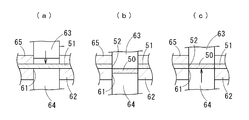
- the press machine as shown in FIG. 2 (a), the die 62 and the punch 63 having the forming hole 61 for forming the metal base plate 51 into the outer shape of the metal plate 50 and the forming hole 61 of the die 62 are fitted.
- a combined pushback mold 64 is provided.
- reference numeral 65 denotes a plate presser that presses the metal base plate on the surface of the die 62.
- the punch 63 descends while pushing down the pushback die 64 in the forming hole 61 of the die 62.
- the metal base plate 51 is punched between the inner peripheral edge of the forming hole 61 of the die 62 as shown in FIG.
- the pushback die 64 is raised so as to follow the rise of the punch 63, and the punched metal plate 50 is pushed back into the punching hole 52 of the original metal base plate 51 as shown in FIG.
- the metal base plate 51 after the punching holes 52 are formed is called a skeleton). At this time, as indicated by an arrow in FIG.
- the punched metal plate 50 is pushed up in the direction opposite to the punching direction and punched with the inner peripheral surface of the punching hole 52 of the metal base plate (skeleton) 51. Further, a shaving action is caused by rubbing against the outer peripheral surface of the metal plate 50. Thereby, the burr
- the metal plate 50 pushed back into the punching hole 52 of the metal base plate (skeleton) 51 is then extracted from the punching hole 52.
- the peripheral portion of one surface of the metal plate 50 becomes a sloping surface 55, and a burr 56 is generated on the peripheral surface of the other surface.
- the side surface 55 is a shear surface 57 having a small surface roughness
- the side where the burr 56 is generated is a fracture surface 58 having a large surface roughness.
- flash 56 obtained by measuring in the several places of the periphery of the metal plate 50 shall be 0.021 mm or less, and the thickness (dimension of a punching direction) of the fracture surface 58 is 0. 068 mm or more.
- the tip of the punch 63 is inserted into the forming hole 61 of the die 62 so that the metal plate 50 is removed from the metal base plate 51.
- the punch 63 may be lowered until it is completely separated, but the lowering of the punch 63 is stopped at a stage where the tip of the punch 63 does not reach the opening end of the forming hole 61 of the die 62 (half-drawn state), and the metal base plate 51 It is also possible to break the metal plate 50 from the metal base plate 51 by biting the punch 63 up to most of the plate thickness, and it may be pushed back in that state.
- FIG. 3 schematically shows a state in which the metal plate 50 described above is laminated on the ceramic substrate 11.
- the surface of the metal plate 50 on which the burrs 56 are generated is superposed on the brazing material layer 59 of the ceramic substrate 11 to form a laminate 40 of the ceramic substrate 11, the brazing material layer 59 and the copper plate 12.
- a plurality of laminated bodies 40 are stacked while being sandwiched between plate-like cushion sheets 30 made of carbon graphite or the like, and 0.05 MPa to 1.0 MPa, for example, in the stacking direction by a pressing jig 110 as shown in FIG. Pressurized with.
- the pressurizing jig 110 includes a base plate 111, guide posts 112 vertically attached to the four corners of the upper surface of the base plate 111, a fixed plate 113 fixed to the upper ends of the guide posts 112, and these base plates 111, a pressing plate 114 supported by a guide post 112 so as to be movable up and down between the fixing plate 113, a spring provided between the fixing plate 113 and the pressing plate 114 and biasing the pressing plate 114 downward
- the above-mentioned laminated body 40 is disposed between the base plate 111 and the pressing plate 114.
- the brazing of the ceramic substrate 11 and the copper plate 12 is a joining using an active metal brazing material, and Ti, which is an active metal in the brazing material, preferentially diffuses into the ceramic substrate 11 to form TiN.
- Ti which is an active metal in the brazing material, preferentially diffuses into the ceramic substrate 11 to form TiN.
- the copper plate 12 and the ceramic substrate 11 are joined via the Cu alloy.
- the pressure jig 110 and the pressure jig 110 are placed in a heating furnace (not shown), and the temperature is 630 ° C. or higher and 650 ° C. or lower for 1 minute in a vacuum atmosphere.
- the ceramic substrate 11 and the aluminum plate 13 are brazed by heating for ⁇ 60 minutes.
- the copper plate 12 and the aluminum plate 13 are bonded to the ceramic substrate 11 with the surface on which the burrs 56 are generated.
- the part is strongly pressed, and the burr 56 prevents the brazing material, which is a bonding material, from flowing out from the bonding interface during melting, and even if a part of the molten brazing flows out, the copper plate 12 and the aluminum plate 13 Since the fractured surfaces 58 at the time of cutting from the metal base plate 51 are arranged so as to be in contact with the surface of the ceramic substrate 11, it is possible to prevent the melting brazing from creeping up the fractured surfaces 58. For this reason, it is possible to prevent the occurrence of wax spots on the surface opposite to the joint surface of the copper plate 12 and the aluminum plate 13.
- the soldering stain on the surface of the copper plate 12 serving as the circuit layer is particularly suppressed, the solderability of the semiconductor chip 14 mounted thereon can be improved.
- flash 56 is restrained to 0.021 mm or less, the joining property between the copper plate 12 and the aluminum plate 13, and the ceramic substrate 11 is not impaired.
- a 30 mm x 30 mm rectangular aluminum nitride plate having a thickness of 0.635 mm is used as the ceramic substrate, and a 27 mm x 27 mm rectangular shape is obtained by stamping and forming a metal base plate (oxygen-free copper plate).
- a copper plate having a thickness of 0.3 mm was used.
- Table 1 shows the half-punch amount of the pushback in each example and comparative example (pushing amount of the punch against the metal base plate).
- the side surface shape of the punched copper plate was observed, the minimum thickness of the fracture surface was measured with a laser microscope, and the average value was calculated from five samples for each example and comparative example. Further, the surface of the copper plate was observed, the maximum burr height was measured with a laser microscope, and an average value was calculated from each of five samples.
- a brazing filler metal layer made of Ag-8.8 mass% Ti was formed on the surface of the aluminum nitride plate.
- the brazing material was formed so that the entire circumference was about 0.2 mm larger than the copper plate.
- the solder stain is a solidified Ag-Cu molten liquid phase formed on the surface of the copper plate along the side surface from the joint interface, and has a thickness of less than 5 ⁇ m. Cannot be measured. For this reason, spots with a width of 1 mm or more from the periphery of the copper plate that can be grasped with the naked eye were counted as wax stains.
- the bonding interface between the copper plate and the ceramic plate should be observed with an ultrasonic image measuring machine, and the area of voids (voids) at the bonding interface should be measured and bonded.
- the total area of voids relative to the area (area of the copper plate) was calculated as a void ratio, and those with a void ratio of less than 2% were judged good and those with a void percentage exceeding 2% were judged as bad.
- the circuit layer is a copper plate and the heat dissipation layer is an aluminum plate, but the present invention is not limited to this combination.
- Both the circuit layer and the heat dissipation layer can be made of the same metal plate, for example, an aluminum plate. In that case, the metal plate can be bonded to both surfaces of the ceramic substrate in a single bonding step.
- ⁇ Suppresses the occurrence of wax spots without impairing the bondability between the metal plate and the ceramic substrate, and improves the solder bondability of the semiconductor chip.
- Power Module Substrate 11 Ceramic Substrate 12 Copper Plate (Metal Plate) 13 Aluminum plate (metal plate) 14 Semiconductor chip 15 Heat sink 40 Laminate 30 Cushion sheet 50 Metal plate 51 Metal base plate 52 Punched hole 55 Draft surface 56 Burr 57 Shear surface 58 Fracture surface 59 Brazing material layer 61 Molding hole 62 Die 63 Punch 64 Pushback die 65 Plate presser 110 Pressing jig 111 Base plate 112 Guide post 113 Fixing plate 114 Pressing plate 115 Biasing means
Landscapes
- Chemical & Material Sciences (AREA)
- Engineering & Computer Science (AREA)
- Ceramic Engineering (AREA)
- Materials Engineering (AREA)
- Structural Engineering (AREA)
- Organic Chemistry (AREA)
- Mechanical Engineering (AREA)
- Cooling Or The Like Of Semiconductors Or Solid State Devices (AREA)
- Ceramic Products (AREA)
Abstract
金属板とセラミックス基板との接合性を損なうことなく、ろうシミの発生を抑制し、半導体チップのはんだ接合性を高めることを目的とし、金属素板のプレス加工により打ち抜き成形された金属板をセラミックス基板の一方の面に積層してろう付けにより接合するパワーモジュール用基板の製造方法であって、前記金属板のバリの高さを0.021mm以下、破断面の厚さを0.068mm以上とし、前記バリが生じている側の表面をセラミックス基板の一方の面に重ねるように前記金属板を前記セラミックス基板上に積層してろう付けする。
Description
本発明は、大電流、高電圧を制御する半導体装置に用いられるパワーモジュール用基板の製造方法に関する。
本願は、2014年8月5日に日本国に出願された特願2014-159337号に基づき優先権を主張し、その内容をここに援用する。
車載用パワーモジュールには、窒化アルミニウムを始めとするセラミックス基板の上に金属板が積層されたパワーモジュール用基板が用いられる。この金属板は、セラミックス基板の両面に積層され、その一方が回路層となり、他方が放熱層となる。回路層には銅板又はアルミニウム板が用いられ、放熱層にはアルミニウム板が用いられるのが一般的である。
例えば、特許文献1及び特許文献2には、セラミックス基板の一方の面に銅板が接合され、他方の面にはアルミニウム板が接合された回路基板が開示されている。この場合、セラミックス基板と銅板とはAg-Cu-Ti系の活性金属を用いたろう材により接合され、セラミックス基板とアルミニウム板とはAl-Si系ろう材により接合される。
このパワーモジュール用基板は以下のように製造される。まず、セラミックス基板の一方の面に、セラミックスと銅板との接合に適するAg-Cu-Ti等の活性金属ろう材を介して銅板を積層し、所定の圧力で加圧しながら、ろう材が溶融する温度以上に加熱し、これによりセラミックス基板と銅板とを接合する。次に、セラミックス基板の他方の面に、セラミックスとアルミニウム板との接合に適するAl-Si系ろう材を介してアルミニウム板を積層し、所定の圧力で加圧しながら、ろう材が溶融する温度以上に加熱し、これによりセラミックス基板とアルミニウム板とを接合する。
このようなパワーモジュール用基板は、銅板の上にはんだ材を介してパワー素子の半導体チップが搭載される。
このようなパワーモジュール用基板において、銅板とセラミックス基板との接合に用いられる活性金属ろうはペーストの形態で供給されるが、このろうペーストと銅の母材とによってAg-Cu溶融ろうを発生させる。この溶融ろうが銅板とセラミックス基板との間から染み出して銅板の側面を伝って這い上がる現象が生じる。表面に這い上がった溶融ろうは、いわゆるろうシミとなり外観を損なうだけでなく、半導体チップを接合する際に用いるはんだ材の濡れ性の悪化につながることが懸念される。回路層にアルミニウム板を用いる場合も同様に、溶融ろうの這い上がりによるろうシミの問題がある。このろうシミの発生を抑制しようとすると、接合性を損なうおそれがある。
本発明は、このような事情に鑑みてなされたもので、金属板とセラミックス基板との接合性を損なうことなく、ろうシミの発生を抑制し、半導体チップのはんだ接合性を高めることを目的とする。
金属板をプレスで打ち抜き作製すると、プレス金型のクリアランスによりバリが発生する。このバリが所定の高さで発生していると、ろうシミの発生を抑制する効果があることがわかった。この場合、側面のうちバリが生じている側は、表面粗さの大きい破断面となる。このため、この破断面をセラミックス基板に近接させることにより、溶融ろうが金属板を這い上がりにくくなるものと考えられる。また、バリによって金属板の周縁がセラミックス基板に強く圧接されることにより、接合面から外部への溶融ろうの流出も抑制されるものと考えられる。これらバリの高さと破断面の厚さとを適切に設定することにより、接合性を損なうことなくろうシミを抑制することができることを見出した。
すなわち、本発明のパワーモジュール用基板の製造方法は、金属素板のプレス加工により打ち抜き成形された金属板をセラミックス基板の一方の面に積層してろう付けにより接合するパワーモジュール用基板の製造方法であって、前記金属板の前記打ち抜き成形によるバリの高さを0.021mm以下とするとともに、破断面の厚さを0.068mm以上とし、前記バリが生じている側の表面(バリ面)を前記セラミックス基板の一方の面に重ねるように積層してろう付けする。
この場合、バリの高さが0.021mmを超えると、高さのばらつきが大きくなって溶融ろうの一部が流出するおそれがあるとともに、接合時の加圧力が全面的に作用しなくなることにより接合性を損なうおそれがある。また、金属板の側面の破断面の厚さ(打ち抜き方向の寸法)が0.068mm以上形成されることにより、わずかに溶融ろうがはみ出したとしても破断面の表面粗さが大きいことにより這い上がりが防止される。破断面の厚さが0.068mm未満であると、ろうシミの発生を抑制することが困難になる。
バリの高さは、金属板の周縁の複数個所を測定して得られる最大値であり、破断面の厚さは、金属板の側面の複数個所を測定して得られる最小値である。なお、粗さ曲線要素の平均高さRcが5μm以上である部分を破断面とした。
本発明のパワーモジュール用基板の製造方法において、プレス加工により前記金属素板から前記金属板を打ち抜き成形する際に、打ち抜いた前記金属板を、打ち抜き後の前記金属素板の打ち抜き孔内にプッシュバックした後、前記打ち抜き孔から前記金属板を抜き出すとよい。
あるいは、前記プレス加工により前記金属素板から前記金属板を打ち抜き成形する際に、前記金属素板を半抜きした状態からプッシュバックした後に、前記金属板を前記金属素板から打ち抜いてもよい。
いわゆるプッシュバックにより金属板を成形することにより、一方向の打ち抜きにより金属板を成形する場合に比べて、バリ及び破断面の大きさを適切に制御することができる。したがって、半抜き工程やプッシュバックを適切に設定することにより、バリの高さを0.021mm以下、破断面の厚さを0.068mm以上に容易に制御することができる。
この場合、プッシュバックは、金属板を完全に打ち抜いた後、厚さの全体が打ち抜き孔に嵌合するようにしてもよいし、厚さの一部が嵌合するようにしてもよい。また、金属素板の厚さの半分程度までプレスする半抜き状態にして、これを押し戻してもよい。
前記金属板は、銅板又はアルミニウム板のいずれも適用することができる。
金属板に銅板を用いる場合は、Ag-Ti、Ag-Cu-Ti等の活性金属ろう材によりセラミックス基板に接合される。金属板にアルミニウム板を用いる場合は、Al-Si系等のろう材により接合される。
本発明によれば、金属板とセラミックス基板との接合性を損なうことなく、金属板の側面に溶融ろうが這い上がる現象が抑制され、ろうシミの発生が抑制され、金属板上に搭載される半導体チップのはんだ接合性も向上する。
以下、本発明の実施形態について、図面を参照しながら説明する。
パワーモジュール用基板10は、図1に示すように、セラミックス基板11の一方の面に、回路層となる銅板(金属板)12が厚さ方向に積層され、セラミックス基板11の他方の面に放熱層となるアルミニウム板(金属板)13が厚さ方向に積層され、これらがろう材によって接合されている。銅板12の表面にははんだ付けにより半導体チップ14が搭載され、アルミニウム板13にはヒートシンク15が接合される。
セラミックス基板11は、窒化アルミニウム(AlN)、アルミナ(Al2O3)、窒化珪素(Si3N4)等により、例えば0.25mm~1.0mmの厚さに形成される。また、銅板12は無酸素銅やタフピッチ銅等の純銅又は銅合金により形成され、アルミニウム板13は純度99.00%以上の純アルミニウム又はアルミニウム合金により形成されている。これら銅板12及びアルミニウム板13の厚さは、例えば0.1mm~10mmとされる。
本実施形態のパワーモジュール用基板10の好ましい組み合わせ例としては、例えばセラミックス基板11が厚み0.635mmのAlN、銅板12が厚み0.3mmの純銅板、アルミニウム板13が厚み1.6mmの4N-アルミニウム板で構成される。
セラミックス基板11と銅板12との接合には、Ag-Ti系又はAg-Cu-Ti系の活性金属ろう材、例えばAg-27.4質量%Cu-2.0質量%Tiのろう材が用いられる。セラミックス基板11とアルミニウム板13との接合には、Al-Si系又はAl-Ge系のろう材が用いられる。
以下、これらセラミックス基板11、銅板12及びアルミニウム板13を接合してパワーモジュール用基板10を製造する方法について説明する。
<金属板成形工程>
銅板12及びアルミニウム板13は、プレス加工により打ち抜き成形される。いずれも同じ方法であるので、この成形工程においては、銅板12及びアルミニウム板13を金属板50として説明する。
銅板12及びアルミニウム板13は、プレス加工により打ち抜き成形される。いずれも同じ方法であるので、この成形工程においては、銅板12及びアルミニウム板13を金属板50として説明する。
金属板50を形成し得る大きさのコイル状の金属素板51を用意し、その金属素板51をコイルから繰り出して間欠的に搬送しながらプレス機に送り込む。プレス機では、図2(a)に示すように、金属素板51を金属板50の外形に成形するための成形孔61を有するダイ62及びパンチ63と、ダイ62の成形孔61内に嵌合したプッシュバック型64とが設けられている。この図2において符号65は、ダイ62の表面で金属素板を押さえる板押さえを示す。
そして、図2(a)に示すようにダイ62とパンチ63との間に金属素板51が送り込まれると、パンチ63が下降し、ダイ62の成形孔61内のプッシュバック型64を押し下げながら金属素板51を図2(b)に示すようにダイ62の成形孔61の内周縁との間で打ち抜く。打ち抜き後、パンチ63の上昇に追従するようにプッシュバック型64が上昇して、図2(c)に示すように打ち抜いた金属板50を元の金属素板51の打ち抜き孔52内に押し戻す(この打ち抜き孔52が形成された後の金属素板51をスケルトンと称す)。このとき、図2(c)に矢印で示すように、打ち抜かれた金属板50が打ち抜き方向とは逆方向に押し上げられ、金属素板(スケルトン)51の打ち抜き孔52の内周面と打ち抜かれた金属板50の外周面とが擦れ合うことによるシェービング作用が生じる。これにより、打ち抜きにより金属板50の外周縁に生じていたバリが、打ち抜き孔52の内周面で削り取られて、削減する。
金属素板(スケルトン)51の打ち抜き孔52に押し戻された金属板50は、その後、打ち抜き孔52から抜き出される。
このようにして金属板50をプレス加工することにより、金属板50の一方の面の周縁部はだれ面55となり、他方の面の周縁にはバリ56が発生する。また、側面において、だれ面55側は表面粗さの小さいせん断面57、バリ56が発生している側は表面粗さの大きい破断面58となる。そして、この金属板50では、金属板50の周縁の複数個所で測定して得られるバリ56の高さが0.021mm以下とされ、破断面58の厚さ(打ち抜き方向の寸法)が0.068mm以上とされる。
なお、金属素板51から金属板50を打ち抜く際に、図2(b)に示すように、パンチ63の先端をダイ62の成形孔61内に挿入して金属板50を金属素板51から完全に切り離すまでパンチ63を下降させてもよいが、パンチ63の先端がダイ62の成形孔61の開口端まで到達しない段階(半抜き状態)でパンチ63の下降を停止し、金属素板51の板厚の大部分までパンチ63を食い込ませることによっても金属板50を金属素板51から破断することが可能であり、その状態で押し戻してもよい。
<銅板接合工程>
前記金属板成形工程によって作製された金属板50のうち銅板12を、ペースト又は箔からなる活性金属ろう材を介在させてセラミックス基板11の一方の面に積層する。このとき、金属板成形工程においてバリ56が発生している側の表面をセラミックス基板11の表面に重ね合わせる。図3に前述した金属板50をセラミックス基板11に積層する状態を模式的に示す。金属板50のバリ56が生じている面をセラミックス基板11のろう材層59に重ね合わせ、セラミックス基板11、ろう材層59および銅板12の積層体40を形成する。
前記金属板成形工程によって作製された金属板50のうち銅板12を、ペースト又は箔からなる活性金属ろう材を介在させてセラミックス基板11の一方の面に積層する。このとき、金属板成形工程においてバリ56が発生している側の表面をセラミックス基板11の表面に重ね合わせる。図3に前述した金属板50をセラミックス基板11に積層する状態を模式的に示す。金属板50のバリ56が生じている面をセラミックス基板11のろう材層59に重ね合わせ、セラミックス基板11、ろう材層59および銅板12の積層体40を形成する。
そして、複数の積層体40をカーボングラファイト等からなる板状のクッションシート30の間にそれぞれ挟んで積み重ね、図4に示すような加圧治具110によって積層方向に例えば0.05MPa~1.0MPaで加圧した状態とする。
この加圧治具110は、ベース板111と、ベース板111の上面の四隅に垂直に取り付けられたガイドポスト112と、これらガイドポスト112の上端部に固定された固定板113と、これらベース板111と固定板113との間で上下移動自在にガイドポスト112に支持された押圧板114と、固定板113と押圧板114との間に設けられて押圧板114を下方に付勢するばね等の付勢手段115とを備え、ベース板111と押圧板114との間に前述の積層体40が配設される。
そして、この加圧治具110により積層体40を加圧した状態で、加圧治具110ごと加熱炉(図示略)内に設置し、真空雰囲気中で800℃以上930℃以下の温度で1分~60分加熱することによりセラミックス基板11と銅板12とをろう付けする。
セラミックス基板11と銅板12とのろう付けは、活性金属ろう材を用いた接合であり、ろう材中の活性金属であるTiがセラミックス基板11に優先的に拡散してTiNを形成し、Ag-Cu合金を介して銅板12とセラミックス基板11とを接合する。
<アルミニウム板接合工程>
銅板12を接合した後のセラミックス基板11の銅板接合面とは反対面を必要に応じて酸洗等により清浄にした後、その表面にろう材を介在させた状態で、前記金属板成形工程によって作製されたアルミニウム板13を積層する。銅板12を接合したセラミックス基板11、ろう材およびアルミニウム板13の積層体を複数、それぞれ前述したクッションシート30の間に挟んで積み重ね、加圧治具110により積層方向に例えば0.3MPa~1.0MPaで加圧する。このときも、アルミニウム板13(金属板50)のバリ56が発生している側の表面をセラミックス基板11に重ね合わせる。
銅板12を接合した後のセラミックス基板11の銅板接合面とは反対面を必要に応じて酸洗等により清浄にした後、その表面にろう材を介在させた状態で、前記金属板成形工程によって作製されたアルミニウム板13を積層する。銅板12を接合したセラミックス基板11、ろう材およびアルミニウム板13の積層体を複数、それぞれ前述したクッションシート30の間に挟んで積み重ね、加圧治具110により積層方向に例えば0.3MPa~1.0MPaで加圧する。このときも、アルミニウム板13(金属板50)のバリ56が発生している側の表面をセラミックス基板11に重ね合わせる。
そして、この加圧治具110により積層体を加圧した状態で、加圧治具110ごと加熱炉(図示略)内に設置し、真空雰囲気中で630℃以上650℃以下の温度で1分~60分加熱することにより、セラミックス基板11とアルミニウム板13とをろう付けする。
このようにして製造されるパワーモジュール用基板10は、銅板12及びアルミニウム板13が、バリ56が生じていた面をセラミックス基板11に向けて接合されるので、それぞれの接合工程において、バリ56の部分が強く押圧され、接合材であるろう材が溶融時に接合界面から外部に流出することがバリ56によって妨げられるとともに、一部の溶融ろうが外部に流出したとしても銅板12及びアルミニウム板13の金属素板51からの切断時の破断面58がそれぞれセラミックス基板11の表面に接触するように配置されているため、この破断面58を溶融ろうが這い上がることが抑制される。このため、銅板12及びアルミニウム板13の接合面とは反対側の表面にろうシミが生じることを防止することができる。
したがって、特に回路層となる銅板12の表面のろうシミが抑制されることから、その上に搭載される半導体チップ14のはんだ接合性を向上させることができる。なお、バリ56の高さを0.021mm以下に抑えているので、銅板12及びアルミニウム板13とセラミックス基板11との間の接合性を損なうこともない。
次に、本発明の効果を確認するために行った確認実験について説明する。
セラミックス基板として30mm×30mmの矩形状で厚さ0.635mmの窒化アルミニウム板を用い、金属素板(無酸素銅板)のプレス加工により打ち抜き成形された金属板(銅板)として27mm×27mmの矩形状で厚さ0.3mmの銅板を用いた。銅板については、表1に示すように、半抜き状態までプレスした後押し戻すプッシュバックによる試料、およびプッシュバックしないで1回のプレスで打抜いた試料を作製した。各実施例、比較例におけるプッシュバックの半抜き量(金属素板に対するパンチの押し込み量)を表1に示す。
打ち抜いた銅板の側面形状を観察し、レーザー顕微鏡にて破断面の最小厚さを測定し、各実施例、比較例について5個の試料から平均値を算出した。また、銅板の表面を観察し、レーザー顕微鏡で最大バリ高さを測定し、各5個の試料から平均値を算出した。
そして、窒化アルミニウム板の表面にAg-8.8質量%Tiからなるろう材層を形成した。ろう材は銅板に対し全周が0.2mm程大きくなるように形成した。銅板のバリが生じている側を窒化アルミニウム板のろう材層の表面に重ねてこれら部材を積層し、1kgf/cm2(約0.1MPa)の圧力で加圧したまま、830℃で30分保持した。
ここでろうシミは、接合界面から側面を伝って銅板の表面上に廻り込み形成されたAg-Cu溶融液相が凝固したものであり、厚さが5μm未満であるため、表面上の凹凸としては測定できない。このため、肉眼で把握できる銅板の周縁から幅1mm以上のシミをろうシミとしてカウントし、その発生率が0%であれば良、ろうシミが少しでも認められたものは不良とした。
また、銅板とセラミックス板との接合性については、超音波画像測定機により、銅板とセラミックス板との接合界面を観察して、接合界面におけるボイド(空孔)の面積を測定し、接合すべき面積(銅板の面積)に対するボイドの合計面積をボイド率として算出し、ボイド率が2%未満であったものを良、2%を超えるものを不良とした。
これらの結果を表1に示す。

表1から明らかなように、銅板のバリの高さが0.021mm以下であると接合性が良好であり、破断面の厚さが0.068mm以上であると、ろうシミの発生が押さえられた。
なお、本発明は、上記実施形態の構成のものに限定されるものではなく、細部構成においては、本発明の趣旨を逸脱しない範囲において種々の変更を加えることが可能である。
上記実施形態では、回路層を銅板、放熱層をアルミニウム板としたが、この組み合わせに限定されるものではない。回路層及び放熱層ともに同種の金属板、例えばアルミニウム板とすることも可能である。その場合は、セラミックス基板の両面に対して金属板を1回の接合工程で接合することが可能である。
金属板とセラミックス基板との接合性を損なうことなく、ろうシミの発生を抑制し、半導体チップのはんだ接合性を高める。
10 パワーモジュール用基板
11 セラミックス基板
12 銅板(金属板)
13 アルミニウム板(金属板)
14 半導体チップ
15 ヒートシンク
40 積層体
30 クッションシート
50 金属板
51 金属素板
52 打ち抜き孔
55 だれ面
56 バリ
57 せん断面
58 破断面
59 ろう材層
61 成形孔
62 ダイ
63 パンチ
64 プッシュバック型
65 板押さえ
110 加圧治具
111 ベース板
112 ガイドポスト
113 固定板
114 押圧板
115 付勢手段
11 セラミックス基板
12 銅板(金属板)
13 アルミニウム板(金属板)
14 半導体チップ
15 ヒートシンク
40 積層体
30 クッションシート
50 金属板
51 金属素板
52 打ち抜き孔
55 だれ面
56 バリ
57 せん断面
58 破断面
59 ろう材層
61 成形孔
62 ダイ
63 パンチ
64 プッシュバック型
65 板押さえ
110 加圧治具
111 ベース板
112 ガイドポスト
113 固定板
114 押圧板
115 付勢手段
Claims (4)
- 金属素板のプレス加工により打ち抜き成形された金属板をセラミックス基板の一方の面に積層してろう付けにより接合するパワーモジュール用基板の製造方法であって、
前記金属板の前記打ち抜き成形によるバリの高さを0.021mm以下とするとともに、破断面の厚さを0.068mm以上とし、前記バリが生じている側の表面を前記セラミックス基板の一方の面に重ねるように積層してろう付けすること
を特徴とするパワーモジュール用基板の製造方法。 - 前記プレス加工により前記金属素板から前記金属板を打ち抜き成形する際に、打ち抜いた前記金属板を、打ち抜き後の前記金属素板の打ち抜き孔内にプッシュバックした後、前記打ち抜き孔から前記金属板を抜き出すことを特徴とする請求項1記載のパワーモジュール用基板の製造方法。
- 前記プレス加工により前記金属素板から前記金属板を打ち抜き成形する際に、前記金属素板を半抜きした状態からプッシュバックした後に、前記金属板を前記金属素板から打ち抜くことを特徴とする請求項1記載のパワーモジュール用基板の製造方法。
- 前記金属板は銅板又はアルミニウム板であることを特徴とする請求項1記載のパワーモジュール用基板の製造方法。
Priority Applications (4)
| Application Number | Priority Date | Filing Date | Title |
|---|---|---|---|
| EP15829203.7A EP3196928B1 (en) | 2014-08-05 | 2015-07-31 | Method for manufacturing substrate for power module |
| KR1020177004802A KR101759056B1 (ko) | 2014-08-05 | 2015-07-31 | 파워 모듈용 기판의 제조 방법 |
| US15/501,632 US20170229320A1 (en) | 2014-08-05 | 2015-07-31 | Producing method of power-module substrate |
| CN201580041285.6A CN106575639B (zh) | 2014-08-05 | 2015-07-31 | 功率模块用基板的制造方法 |
Applications Claiming Priority (2)
| Application Number | Priority Date | Filing Date | Title |
|---|---|---|---|
| JP2014-159337 | 2014-08-05 | ||
| JP2014159337A JP5954371B2 (ja) | 2014-08-05 | 2014-08-05 | パワーモジュール用基板及びその製造方法 |
Publications (1)
| Publication Number | Publication Date |
|---|---|
| WO2016021491A1 true WO2016021491A1 (ja) | 2016-02-11 |
Family
ID=55263759
Family Applications (1)
| Application Number | Title | Priority Date | Filing Date |
|---|---|---|---|
| PCT/JP2015/071776 Ceased WO2016021491A1 (ja) | 2014-08-05 | 2015-07-31 | パワーモジュール用基板の製造方法 |
Country Status (7)
| Country | Link |
|---|---|
| US (1) | US20170229320A1 (ja) |
| EP (1) | EP3196928B1 (ja) |
| JP (1) | JP5954371B2 (ja) |
| KR (1) | KR101759056B1 (ja) |
| CN (1) | CN106575639B (ja) |
| TW (1) | TWI612622B (ja) |
| WO (1) | WO2016021491A1 (ja) |
Cited By (3)
| Publication number | Priority date | Publication date | Assignee | Title |
|---|---|---|---|---|
| JP2017163074A (ja) * | 2016-03-11 | 2017-09-14 | 三菱マテリアル株式会社 | パワーモジュール用基板の製造方法 |
| WO2018110104A1 (ja) * | 2016-12-16 | 2018-06-21 | Jx金属株式会社 | 回路基板用金属板、回路基板、パワーモジュール、金属板成形品及び、回路基板の製造方法 |
| CN113745169A (zh) * | 2021-07-23 | 2021-12-03 | 中国电子科技集团公司第二十九研究所 | 多腔槽ltcc基板与封装盒体焊接结构及方法 |
Families Citing this family (16)
| Publication number | Priority date | Publication date | Assignee | Title |
|---|---|---|---|---|
| JP6760158B2 (ja) * | 2017-03-21 | 2020-09-23 | 三菱マテリアル株式会社 | 金属−セラミックス接合基板及びその製造方法 |
| WO2019003725A1 (ja) * | 2017-06-28 | 2019-01-03 | 京セラ株式会社 | パワーモジュール用基板およびパワーモジュール |
| JP7147232B2 (ja) * | 2018-04-09 | 2022-10-05 | 三菱マテリアル株式会社 | セラミックス-金属接合体の製造方法、多数個取り用セラミックス-金属接合体の製造方法、セラミックス-金属接合体及び多数個取り用セラミックス-金属接合体 |
| US11996299B2 (en) * | 2018-10-23 | 2024-05-28 | Mitsubishi Electric Corporation | Methods for manufacturing a semiconductor device |
| CN109534842B (zh) * | 2018-11-26 | 2021-08-10 | 北京卫星制造厂有限公司 | 功率半导体模块用焊接工艺 |
| JP7212700B2 (ja) | 2018-12-28 | 2023-01-25 | デンカ株式会社 | セラミックス-銅複合体、セラミックス回路基板、パワーモジュール及びセラミックス-銅複合体の製造方法 |
| JP2020141125A (ja) * | 2019-02-26 | 2020-09-03 | 日本発條株式会社 | 回路基板用半製品板材の製造方法、回路基板用半製品板材、及び金属ベース回路基板の製造方法 |
| CN111615266A (zh) * | 2019-02-26 | 2020-09-01 | 日本发条株式会社 | 电路基板用半制品板材的制造方法、电路基板用半制品板材及金属基体电路基板的制造方法 |
| JP7272018B2 (ja) * | 2019-03-08 | 2023-05-12 | 三菱マテリアル株式会社 | 絶縁回路基板の製造方法 |
| EP4177943B1 (en) * | 2020-07-02 | 2024-12-25 | Amosense Co.,Ltd | Power module, and method for manufacturing same |
| JP7548770B2 (ja) * | 2020-10-16 | 2024-09-10 | Shプレシジョン株式会社 | 金属回路パターンおよび金属回路パターンの製造方法 |
| JP7574697B2 (ja) * | 2021-03-01 | 2024-10-29 | 三菱マテリアル株式会社 | 絶縁回路基板の製造方法 |
| JP2022163250A (ja) * | 2021-04-14 | 2022-10-26 | 矢崎総業株式会社 | 端子付き電線、及び、金属端子 |
| JP2023066874A (ja) * | 2021-10-29 | 2023-05-16 | 三菱マテリアル株式会社 | 銅/セラミックス接合体、および、絶縁回路基板 |
| JP7786276B2 (ja) * | 2022-03-24 | 2025-12-16 | 三菱マテリアル株式会社 | 接合体の製造方法 |
| KR102949513B1 (ko) | 2023-05-15 | 2026-04-09 | 코스텍시스템(주) | 칩 접합 장비와 이를 포함하는 칩 접합 시스템 및 그 접합 방법 |
Citations (4)
| Publication number | Priority date | Publication date | Assignee | Title |
|---|---|---|---|---|
| JP2001044312A (ja) * | 1999-07-30 | 2001-02-16 | Ngk Spark Plug Co Ltd | 金属製スティフナ付き配線基板 |
| JP2002353351A (ja) * | 2001-05-30 | 2002-12-06 | Kyocera Corp | 電子部品収納用パッケージ |
| JP2007088365A (ja) * | 2005-09-26 | 2007-04-05 | Sanyo Electric Co Ltd | 回路装置 |
| JP2008311295A (ja) * | 2007-06-12 | 2008-12-25 | Mitsubishi Materials Corp | パワーモジュール用基板の製造方法 |
Family Cites Families (13)
| Publication number | Priority date | Publication date | Assignee | Title |
|---|---|---|---|---|
| JPH07101721B2 (ja) * | 1988-06-03 | 1995-11-01 | 住友特殊金属株式会社 | 集積回路用Agろう付きシールリング及びその製造方法 |
| JPH0783033B2 (ja) * | 1988-11-30 | 1995-09-06 | 太陽誘電株式会社 | 半導体素子固着板状体シート及びその使用方法 |
| DE3931320C1 (ja) * | 1989-09-20 | 1991-08-08 | Feintool International Holding, Lyss, Ch | |
| JPH0973760A (ja) * | 1995-09-07 | 1997-03-18 | Sony Corp | プレート原反の打抜方法とテープカセットのベースプレート |
| JP2003197826A (ja) | 2001-12-26 | 2003-07-11 | Toshiba Corp | セラミックス回路基板およびそれを用いた半導体モジュール |
| JP2005093935A (ja) * | 2003-09-19 | 2005-04-07 | Sumitomo Electric Ind Ltd | スティフナーとその製造方法およびそれを用いた半導体装置 |
| US7464575B2 (en) * | 2004-10-13 | 2008-12-16 | Nakamura Seisakusho Kabushikigaisha | Shearing method for thin plate |
| WO2006080356A1 (ja) * | 2005-01-25 | 2006-08-03 | Aisin Aw Co., Ltd. | プレス加工装置、プレス加工方法、及び打抜き加工品 |
| DE502007005770D1 (de) * | 2007-09-14 | 2011-01-05 | Feintool Ip Ag | Verfahren und Vorrichtung zum Herstellen von Stanzteilen mit vergrösserter Funktionsfläche |
| WO2013018344A1 (ja) * | 2011-07-29 | 2013-02-07 | 三洋電機株式会社 | 素子搭載用基板およびその製造方法、ならびに半導体モジュールおよびその製造方法 |
| EP2743978B1 (en) * | 2011-08-12 | 2018-05-02 | Mitsubishi Materials Corporation | Substrate for power module, substrate for power module with heat sink, power module, and method for manufacturing substrate for power module |
| JP6028352B2 (ja) * | 2012-03-16 | 2016-11-16 | 三菱マテリアル株式会社 | ヒートシンク付パワーモジュール用基板の製造方法 |
| JP2013229579A (ja) * | 2012-03-30 | 2013-11-07 | Mitsubishi Materials Corp | パワーモジュール用基板、ヒートシンク付パワーモジュール用基板及びパワーモジュール |
-
2014
- 2014-08-05 JP JP2014159337A patent/JP5954371B2/ja active Active
-
2015
- 2015-07-31 US US15/501,632 patent/US20170229320A1/en not_active Abandoned
- 2015-07-31 WO PCT/JP2015/071776 patent/WO2016021491A1/ja not_active Ceased
- 2015-07-31 EP EP15829203.7A patent/EP3196928B1/en active Active
- 2015-07-31 CN CN201580041285.6A patent/CN106575639B/zh active Active
- 2015-07-31 KR KR1020177004802A patent/KR101759056B1/ko not_active Expired - Fee Related
- 2015-08-04 TW TW104125217A patent/TWI612622B/zh active
Patent Citations (4)
| Publication number | Priority date | Publication date | Assignee | Title |
|---|---|---|---|---|
| JP2001044312A (ja) * | 1999-07-30 | 2001-02-16 | Ngk Spark Plug Co Ltd | 金属製スティフナ付き配線基板 |
| JP2002353351A (ja) * | 2001-05-30 | 2002-12-06 | Kyocera Corp | 電子部品収納用パッケージ |
| JP2007088365A (ja) * | 2005-09-26 | 2007-04-05 | Sanyo Electric Co Ltd | 回路装置 |
| JP2008311295A (ja) * | 2007-06-12 | 2008-12-25 | Mitsubishi Materials Corp | パワーモジュール用基板の製造方法 |
Cited By (5)
| Publication number | Priority date | Publication date | Assignee | Title |
|---|---|---|---|---|
| JP2017163074A (ja) * | 2016-03-11 | 2017-09-14 | 三菱マテリアル株式会社 | パワーモジュール用基板の製造方法 |
| WO2018110104A1 (ja) * | 2016-12-16 | 2018-06-21 | Jx金属株式会社 | 回路基板用金属板、回路基板、パワーモジュール、金属板成形品及び、回路基板の製造方法 |
| JP2018098467A (ja) * | 2016-12-16 | 2018-06-21 | Jx金属株式会社 | 回路基板用金属板、回路基板、パワーモジュール、金属板成形品及び、回路基板の製造方法 |
| CN113745169A (zh) * | 2021-07-23 | 2021-12-03 | 中国电子科技集团公司第二十九研究所 | 多腔槽ltcc基板与封装盒体焊接结构及方法 |
| CN113745169B (zh) * | 2021-07-23 | 2023-10-24 | 中国电子科技集团公司第二十九研究所 | 多腔槽ltcc基板与封装盒体焊接结构及方法 |
Also Published As
| Publication number | Publication date |
|---|---|
| JP5954371B2 (ja) | 2016-07-20 |
| TW201626510A (zh) | 2016-07-16 |
| EP3196928A4 (en) | 2018-06-20 |
| US20170229320A1 (en) | 2017-08-10 |
| EP3196928B1 (en) | 2019-09-04 |
| KR20170029630A (ko) | 2017-03-15 |
| CN106575639B (zh) | 2019-03-15 |
| JP2016039163A (ja) | 2016-03-22 |
| EP3196928A1 (en) | 2017-07-26 |
| KR101759056B1 (ko) | 2017-07-17 |
| TWI612622B (zh) | 2018-01-21 |
| CN106575639A (zh) | 2017-04-19 |
Similar Documents
| Publication | Publication Date | Title |
|---|---|---|
| JP5954371B2 (ja) | パワーモジュール用基板及びその製造方法 | |
| EP3208839A1 (en) | Substrate with cooler for power modules and method for producing same | |
| JP5125241B2 (ja) | パワーモジュール用基板の製造方法 | |
| JP5077102B2 (ja) | パワーモジュール用基板及びその製造方法 | |
| JP6455056B2 (ja) | ヒートシンク付パワーモジュール用基板の製造方法及び加圧装置 | |
| CN110325310B (zh) | 接合体的制造方法、绝缘电路基板的制造方法及自带散热片的绝缘电路基板的制造方法 | |
| JP2010097963A (ja) | 回路基板及びその製造方法、電子部品モジュール | |
| JP5056186B2 (ja) | パワーモジュール用基板の製造方法 | |
| JP2012146801A (ja) | ヒートシンク、ヒートシンク付パワーモジュール用基板、パワーモジュール及びヒートシンクの製造方法。 | |
| JP6631333B2 (ja) | パワーモジュール用基板の製造方法 | |
| JP5146296B2 (ja) | パワーモジュール用基板の製造方法 | |
| JP5131205B2 (ja) | パワーモジュール用基板の製造方法 | |
| JP2016162926A (ja) | セラミックス基板とアルミニウム板との接合体の製造方法 | |
| JP5887907B2 (ja) | パワーモジュール用基板の製造方法および製造装置 | |
| JP6782375B1 (ja) | 金属回路パターンおよび金属回路パターンの製造方法 | |
| CN114375088B (zh) | 金属电路图案和金属电路图案的制造方法 | |
| JP7272018B2 (ja) | 絶縁回路基板の製造方法 | |
| JP6102271B2 (ja) | ヒートシンク付パワーモジュール用基板の製造方法 | |
| JP7230602B2 (ja) | 絶縁回路基板及びその製造方法 | |
| JP4677948B2 (ja) | パワーモジュール用基板の製造方法 | |
| JP6152681B2 (ja) | パワーモジュール用基板およびその製造方法 | |
| JP2021150558A (ja) | 絶縁回路基板 |
Legal Events
| Date | Code | Title | Description |
|---|---|---|---|
| 121 | Ep: the epo has been informed by wipo that ep was designated in this application |
Ref document number: 15829203 Country of ref document: EP Kind code of ref document: A1 |
|
| NENP | Non-entry into the national phase |
Ref country code: DE |
|
| REEP | Request for entry into the european phase |
Ref document number: 2015829203 Country of ref document: EP |
|
| WWE | Wipo information: entry into national phase |
Ref document number: 1020177004802 Country of ref document: KR Ref document number: 2015829203 Country of ref document: EP |