WO2016035202A1 - 液晶表示装置及び表示装置用基板 - Google Patents
液晶表示装置及び表示装置用基板 Download PDFInfo
- Publication number
- WO2016035202A1 WO2016035202A1 PCT/JP2014/073513 JP2014073513W WO2016035202A1 WO 2016035202 A1 WO2016035202 A1 WO 2016035202A1 JP 2014073513 W JP2014073513 W JP 2014073513W WO 2016035202 A1 WO2016035202 A1 WO 2016035202A1
- Authority
- WO
- WIPO (PCT)
- Prior art keywords
- layer
- liquid crystal
- display device
- wiring layer
- substrate
- Prior art date
- Legal status (The legal status is an assumption and is not a legal conclusion. Google has not performed a legal analysis and makes no representation as to the accuracy of the status listed.)
- Ceased
Links
Images

Classifications
-
- G—PHYSICS
- G02—OPTICS
- G02F—OPTICAL DEVICES OR ARRANGEMENTS FOR THE CONTROL OF LIGHT BY MODIFICATION OF THE OPTICAL PROPERTIES OF THE MEDIA OF THE ELEMENTS INVOLVED THEREIN; NON-LINEAR OPTICS; FREQUENCY-CHANGING OF LIGHT; OPTICAL LOGIC ELEMENTS; OPTICAL ANALOGUE/DIGITAL CONVERTERS
- G02F1/00—Devices or arrangements for the control of the intensity, colour, phase, polarisation or direction of light arriving from an independent light source, e.g. switching, gating or modulating; Non-linear optics
- G02F1/01—Devices or arrangements for the control of the intensity, colour, phase, polarisation or direction of light arriving from an independent light source, e.g. switching, gating or modulating; Non-linear optics for the control of the intensity, phase, polarisation or colour
- G02F1/13—Devices or arrangements for the control of the intensity, colour, phase, polarisation or direction of light arriving from an independent light source, e.g. switching, gating or modulating; Non-linear optics for the control of the intensity, phase, polarisation or colour based on liquid crystals, e.g. single liquid crystal display cells
- G02F1/133—Constructional arrangements; Operation of liquid crystal cells; Circuit arrangements
- G02F1/136—Liquid crystal cells structurally associated with a semi-conducting layer or substrate, e.g. cells forming part of an integrated circuit
- G02F1/1362—Active matrix addressed cells
- G02F1/1368—Active matrix addressed cells in which the switching element is a three-electrode device
-
- G—PHYSICS
- G02—OPTICS
- G02F—OPTICAL DEVICES OR ARRANGEMENTS FOR THE CONTROL OF LIGHT BY MODIFICATION OF THE OPTICAL PROPERTIES OF THE MEDIA OF THE ELEMENTS INVOLVED THEREIN; NON-LINEAR OPTICS; FREQUENCY-CHANGING OF LIGHT; OPTICAL LOGIC ELEMENTS; OPTICAL ANALOGUE/DIGITAL CONVERTERS
- G02F1/00—Devices or arrangements for the control of the intensity, colour, phase, polarisation or direction of light arriving from an independent light source, e.g. switching, gating or modulating; Non-linear optics
- G02F1/01—Devices or arrangements for the control of the intensity, colour, phase, polarisation or direction of light arriving from an independent light source, e.g. switching, gating or modulating; Non-linear optics for the control of the intensity, phase, polarisation or colour
- G02F1/13—Devices or arrangements for the control of the intensity, colour, phase, polarisation or direction of light arriving from an independent light source, e.g. switching, gating or modulating; Non-linear optics for the control of the intensity, phase, polarisation or colour based on liquid crystals, e.g. single liquid crystal display cells
- G02F1/133—Constructional arrangements; Operation of liquid crystal cells; Circuit arrangements
- G02F1/1333—Constructional arrangements; Manufacturing methods
-
- G—PHYSICS
- G02—OPTICS
- G02F—OPTICAL DEVICES OR ARRANGEMENTS FOR THE CONTROL OF LIGHT BY MODIFICATION OF THE OPTICAL PROPERTIES OF THE MEDIA OF THE ELEMENTS INVOLVED THEREIN; NON-LINEAR OPTICS; FREQUENCY-CHANGING OF LIGHT; OPTICAL LOGIC ELEMENTS; OPTICAL ANALOGUE/DIGITAL CONVERTERS
- G02F1/00—Devices or arrangements for the control of the intensity, colour, phase, polarisation or direction of light arriving from an independent light source, e.g. switching, gating or modulating; Non-linear optics
- G02F1/01—Devices or arrangements for the control of the intensity, colour, phase, polarisation or direction of light arriving from an independent light source, e.g. switching, gating or modulating; Non-linear optics for the control of the intensity, phase, polarisation or colour
- G02F1/13—Devices or arrangements for the control of the intensity, colour, phase, polarisation or direction of light arriving from an independent light source, e.g. switching, gating or modulating; Non-linear optics for the control of the intensity, phase, polarisation or colour based on liquid crystals, e.g. single liquid crystal display cells
- G02F1/133—Constructional arrangements; Operation of liquid crystal cells; Circuit arrangements
- G02F1/1333—Constructional arrangements; Manufacturing methods
- G02F1/133345—Insulating layers
-
- G—PHYSICS
- G02—OPTICS
- G02F—OPTICAL DEVICES OR ARRANGEMENTS FOR THE CONTROL OF LIGHT BY MODIFICATION OF THE OPTICAL PROPERTIES OF THE MEDIA OF THE ELEMENTS INVOLVED THEREIN; NON-LINEAR OPTICS; FREQUENCY-CHANGING OF LIGHT; OPTICAL LOGIC ELEMENTS; OPTICAL ANALOGUE/DIGITAL CONVERTERS
- G02F1/00—Devices or arrangements for the control of the intensity, colour, phase, polarisation or direction of light arriving from an independent light source, e.g. switching, gating or modulating; Non-linear optics
- G02F1/01—Devices or arrangements for the control of the intensity, colour, phase, polarisation or direction of light arriving from an independent light source, e.g. switching, gating or modulating; Non-linear optics for the control of the intensity, phase, polarisation or colour
- G02F1/13—Devices or arrangements for the control of the intensity, colour, phase, polarisation or direction of light arriving from an independent light source, e.g. switching, gating or modulating; Non-linear optics for the control of the intensity, phase, polarisation or colour based on liquid crystals, e.g. single liquid crystal display cells
- G02F1/133—Constructional arrangements; Operation of liquid crystal cells; Circuit arrangements
- G02F1/1333—Constructional arrangements; Manufacturing methods
- G02F1/13338—Input devices, e.g. touch panels
-
- G—PHYSICS
- G02—OPTICS
- G02F—OPTICAL DEVICES OR ARRANGEMENTS FOR THE CONTROL OF LIGHT BY MODIFICATION OF THE OPTICAL PROPERTIES OF THE MEDIA OF THE ELEMENTS INVOLVED THEREIN; NON-LINEAR OPTICS; FREQUENCY-CHANGING OF LIGHT; OPTICAL LOGIC ELEMENTS; OPTICAL ANALOGUE/DIGITAL CONVERTERS
- G02F1/00—Devices or arrangements for the control of the intensity, colour, phase, polarisation or direction of light arriving from an independent light source, e.g. switching, gating or modulating; Non-linear optics
- G02F1/01—Devices or arrangements for the control of the intensity, colour, phase, polarisation or direction of light arriving from an independent light source, e.g. switching, gating or modulating; Non-linear optics for the control of the intensity, phase, polarisation or colour
- G02F1/13—Devices or arrangements for the control of the intensity, colour, phase, polarisation or direction of light arriving from an independent light source, e.g. switching, gating or modulating; Non-linear optics for the control of the intensity, phase, polarisation or colour based on liquid crystals, e.g. single liquid crystal display cells
- G02F1/133—Constructional arrangements; Operation of liquid crystal cells; Circuit arrangements
- G02F1/1333—Constructional arrangements; Manufacturing methods
- G02F1/1335—Structural association of cells with optical devices, e.g. polarisers or reflectors
-
- G—PHYSICS
- G02—OPTICS
- G02F—OPTICAL DEVICES OR ARRANGEMENTS FOR THE CONTROL OF LIGHT BY MODIFICATION OF THE OPTICAL PROPERTIES OF THE MEDIA OF THE ELEMENTS INVOLVED THEREIN; NON-LINEAR OPTICS; FREQUENCY-CHANGING OF LIGHT; OPTICAL LOGIC ELEMENTS; OPTICAL ANALOGUE/DIGITAL CONVERTERS
- G02F1/00—Devices or arrangements for the control of the intensity, colour, phase, polarisation or direction of light arriving from an independent light source, e.g. switching, gating or modulating; Non-linear optics
- G02F1/01—Devices or arrangements for the control of the intensity, colour, phase, polarisation or direction of light arriving from an independent light source, e.g. switching, gating or modulating; Non-linear optics for the control of the intensity, phase, polarisation or colour
- G02F1/13—Devices or arrangements for the control of the intensity, colour, phase, polarisation or direction of light arriving from an independent light source, e.g. switching, gating or modulating; Non-linear optics for the control of the intensity, phase, polarisation or colour based on liquid crystals, e.g. single liquid crystal display cells
- G02F1/133—Constructional arrangements; Operation of liquid crystal cells; Circuit arrangements
- G02F1/1333—Constructional arrangements; Manufacturing methods
- G02F1/1335—Structural association of cells with optical devices, e.g. polarisers or reflectors
- G02F1/133509—Filters, e.g. light shielding masks
-
- G—PHYSICS
- G02—OPTICS
- G02F—OPTICAL DEVICES OR ARRANGEMENTS FOR THE CONTROL OF LIGHT BY MODIFICATION OF THE OPTICAL PROPERTIES OF THE MEDIA OF THE ELEMENTS INVOLVED THEREIN; NON-LINEAR OPTICS; FREQUENCY-CHANGING OF LIGHT; OPTICAL LOGIC ELEMENTS; OPTICAL ANALOGUE/DIGITAL CONVERTERS
- G02F1/00—Devices or arrangements for the control of the intensity, colour, phase, polarisation or direction of light arriving from an independent light source, e.g. switching, gating or modulating; Non-linear optics
- G02F1/01—Devices or arrangements for the control of the intensity, colour, phase, polarisation or direction of light arriving from an independent light source, e.g. switching, gating or modulating; Non-linear optics for the control of the intensity, phase, polarisation or colour
- G02F1/13—Devices or arrangements for the control of the intensity, colour, phase, polarisation or direction of light arriving from an independent light source, e.g. switching, gating or modulating; Non-linear optics for the control of the intensity, phase, polarisation or colour based on liquid crystals, e.g. single liquid crystal display cells
- G02F1/133—Constructional arrangements; Operation of liquid crystal cells; Circuit arrangements
- G02F1/1333—Constructional arrangements; Manufacturing methods
- G02F1/1335—Structural association of cells with optical devices, e.g. polarisers or reflectors
- G02F1/133509—Filters, e.g. light shielding masks
- G02F1/133512—Light shielding layers, e.g. black matrix
-
- G—PHYSICS
- G02—OPTICS
- G02F—OPTICAL DEVICES OR ARRANGEMENTS FOR THE CONTROL OF LIGHT BY MODIFICATION OF THE OPTICAL PROPERTIES OF THE MEDIA OF THE ELEMENTS INVOLVED THEREIN; NON-LINEAR OPTICS; FREQUENCY-CHANGING OF LIGHT; OPTICAL LOGIC ELEMENTS; OPTICAL ANALOGUE/DIGITAL CONVERTERS
- G02F1/00—Devices or arrangements for the control of the intensity, colour, phase, polarisation or direction of light arriving from an independent light source, e.g. switching, gating or modulating; Non-linear optics
- G02F1/01—Devices or arrangements for the control of the intensity, colour, phase, polarisation or direction of light arriving from an independent light source, e.g. switching, gating or modulating; Non-linear optics for the control of the intensity, phase, polarisation or colour
- G02F1/13—Devices or arrangements for the control of the intensity, colour, phase, polarisation or direction of light arriving from an independent light source, e.g. switching, gating or modulating; Non-linear optics for the control of the intensity, phase, polarisation or colour based on liquid crystals, e.g. single liquid crystal display cells
- G02F1/133—Constructional arrangements; Operation of liquid crystal cells; Circuit arrangements
- G02F1/1333—Constructional arrangements; Manufacturing methods
- G02F1/1335—Structural association of cells with optical devices, e.g. polarisers or reflectors
- G02F1/133509—Filters, e.g. light shielding masks
- G02F1/133514—Colour filters
-
- G—PHYSICS
- G02—OPTICS
- G02F—OPTICAL DEVICES OR ARRANGEMENTS FOR THE CONTROL OF LIGHT BY MODIFICATION OF THE OPTICAL PROPERTIES OF THE MEDIA OF THE ELEMENTS INVOLVED THEREIN; NON-LINEAR OPTICS; FREQUENCY-CHANGING OF LIGHT; OPTICAL LOGIC ELEMENTS; OPTICAL ANALOGUE/DIGITAL CONVERTERS
- G02F1/00—Devices or arrangements for the control of the intensity, colour, phase, polarisation or direction of light arriving from an independent light source, e.g. switching, gating or modulating; Non-linear optics
- G02F1/01—Devices or arrangements for the control of the intensity, colour, phase, polarisation or direction of light arriving from an independent light source, e.g. switching, gating or modulating; Non-linear optics for the control of the intensity, phase, polarisation or colour
- G02F1/13—Devices or arrangements for the control of the intensity, colour, phase, polarisation or direction of light arriving from an independent light source, e.g. switching, gating or modulating; Non-linear optics for the control of the intensity, phase, polarisation or colour based on liquid crystals, e.g. single liquid crystal display cells
- G02F1/133—Constructional arrangements; Operation of liquid crystal cells; Circuit arrangements
- G02F1/1333—Constructional arrangements; Manufacturing methods
- G02F1/1335—Structural association of cells with optical devices, e.g. polarisers or reflectors
- G02F1/1336—Illuminating devices
- G02F1/133602—Direct backlight
-
- G—PHYSICS
- G02—OPTICS
- G02F—OPTICAL DEVICES OR ARRANGEMENTS FOR THE CONTROL OF LIGHT BY MODIFICATION OF THE OPTICAL PROPERTIES OF THE MEDIA OF THE ELEMENTS INVOLVED THEREIN; NON-LINEAR OPTICS; FREQUENCY-CHANGING OF LIGHT; OPTICAL LOGIC ELEMENTS; OPTICAL ANALOGUE/DIGITAL CONVERTERS
- G02F1/00—Devices or arrangements for the control of the intensity, colour, phase, polarisation or direction of light arriving from an independent light source, e.g. switching, gating or modulating; Non-linear optics
- G02F1/01—Devices or arrangements for the control of the intensity, colour, phase, polarisation or direction of light arriving from an independent light source, e.g. switching, gating or modulating; Non-linear optics for the control of the intensity, phase, polarisation or colour
- G02F1/13—Devices or arrangements for the control of the intensity, colour, phase, polarisation or direction of light arriving from an independent light source, e.g. switching, gating or modulating; Non-linear optics for the control of the intensity, phase, polarisation or colour based on liquid crystals, e.g. single liquid crystal display cells
- G02F1/133—Constructional arrangements; Operation of liquid crystal cells; Circuit arrangements
- G02F1/1333—Constructional arrangements; Manufacturing methods
- G02F1/1343—Electrodes
- G02F1/134309—Electrodes characterised by their geometrical arrangement
- G02F1/134363—Electrodes characterised by their geometrical arrangement for applying an electric field parallel to the substrate, i.e. in-plane switching [IPS]
-
- G—PHYSICS
- G02—OPTICS
- G02F—OPTICAL DEVICES OR ARRANGEMENTS FOR THE CONTROL OF LIGHT BY MODIFICATION OF THE OPTICAL PROPERTIES OF THE MEDIA OF THE ELEMENTS INVOLVED THEREIN; NON-LINEAR OPTICS; FREQUENCY-CHANGING OF LIGHT; OPTICAL LOGIC ELEMENTS; OPTICAL ANALOGUE/DIGITAL CONVERTERS
- G02F1/00—Devices or arrangements for the control of the intensity, colour, phase, polarisation or direction of light arriving from an independent light source, e.g. switching, gating or modulating; Non-linear optics
- G02F1/01—Devices or arrangements for the control of the intensity, colour, phase, polarisation or direction of light arriving from an independent light source, e.g. switching, gating or modulating; Non-linear optics for the control of the intensity, phase, polarisation or colour
- G02F1/13—Devices or arrangements for the control of the intensity, colour, phase, polarisation or direction of light arriving from an independent light source, e.g. switching, gating or modulating; Non-linear optics for the control of the intensity, phase, polarisation or colour based on liquid crystals, e.g. single liquid crystal display cells
- G02F1/133—Constructional arrangements; Operation of liquid crystal cells; Circuit arrangements
- G02F1/136—Liquid crystal cells structurally associated with a semi-conducting layer or substrate, e.g. cells forming part of an integrated circuit
- G02F1/1362—Active matrix addressed cells
- G02F1/136286—Wiring, e.g. gate line, drain line
-
- G—PHYSICS
- G06—COMPUTING OR CALCULATING; COUNTING
- G06F—ELECTRIC DIGITAL DATA PROCESSING
- G06F3/00—Input arrangements for transferring data to be processed into a form capable of being handled by the computer; Output arrangements for transferring data from processing unit to output unit, e.g. interface arrangements
- G06F3/01—Input arrangements or combined input and output arrangements for interaction between user and computer
- G06F3/03—Arrangements for converting the position or the displacement of a member into a coded form
- G06F3/041—Digitisers, e.g. for touch screens or touch pads, characterised by the transducing means
- G06F3/0412—Digitisers structurally integrated in a display
-
- G—PHYSICS
- G06—COMPUTING OR CALCULATING; COUNTING
- G06F—ELECTRIC DIGITAL DATA PROCESSING
- G06F3/00—Input arrangements for transferring data to be processed into a form capable of being handled by the computer; Output arrangements for transferring data from processing unit to output unit, e.g. interface arrangements
- G06F3/01—Input arrangements or combined input and output arrangements for interaction between user and computer
- G06F3/03—Arrangements for converting the position or the displacement of a member into a coded form
- G06F3/041—Digitisers, e.g. for touch screens or touch pads, characterised by the transducing means
- G06F3/0416—Control or interface arrangements specially adapted for digitisers
- G06F3/0418—Control or interface arrangements specially adapted for digitisers for error correction or compensation, e.g. based on parallax, calibration or alignment
- G06F3/04184—Synchronisation with the driving of the display or the backlighting unit to avoid interferences generated internally
-
- G—PHYSICS
- G06—COMPUTING OR CALCULATING; COUNTING
- G06F—ELECTRIC DIGITAL DATA PROCESSING
- G06F3/00—Input arrangements for transferring data to be processed into a form capable of being handled by the computer; Output arrangements for transferring data from processing unit to output unit, e.g. interface arrangements
- G06F3/01—Input arrangements or combined input and output arrangements for interaction between user and computer
- G06F3/03—Arrangements for converting the position or the displacement of a member into a coded form
- G06F3/041—Digitisers, e.g. for touch screens or touch pads, characterised by the transducing means
- G06F3/044—Digitisers, e.g. for touch screens or touch pads, characterised by the transducing means by capacitive means
- G06F3/0445—Digitisers, e.g. for touch screens or touch pads, characterised by the transducing means by capacitive means using two or more layers of sensing electrodes, e.g. using two layers of electrodes separated by a dielectric layer
-
- G—PHYSICS
- G06—COMPUTING OR CALCULATING; COUNTING
- G06F—ELECTRIC DIGITAL DATA PROCESSING
- G06F3/00—Input arrangements for transferring data to be processed into a form capable of being handled by the computer; Output arrangements for transferring data from processing unit to output unit, e.g. interface arrangements
- G06F3/01—Input arrangements or combined input and output arrangements for interaction between user and computer
- G06F3/03—Arrangements for converting the position or the displacement of a member into a coded form
- G06F3/041—Digitisers, e.g. for touch screens or touch pads, characterised by the transducing means
- G06F3/044—Digitisers, e.g. for touch screens or touch pads, characterised by the transducing means by capacitive means
- G06F3/0446—Digitisers, e.g. for touch screens or touch pads, characterised by the transducing means by capacitive means using a grid-like structure of electrodes in at least two directions, e.g. using row and column electrodes
-
- G—PHYSICS
- G06—COMPUTING OR CALCULATING; COUNTING
- G06F—ELECTRIC DIGITAL DATA PROCESSING
- G06F3/00—Input arrangements for transferring data to be processed into a form capable of being handled by the computer; Output arrangements for transferring data from processing unit to output unit, e.g. interface arrangements
- G06F3/01—Input arrangements or combined input and output arrangements for interaction between user and computer
- G06F3/03—Arrangements for converting the position or the displacement of a member into a coded form
- G06F3/041—Digitisers, e.g. for touch screens or touch pads, characterised by the transducing means
- G06F3/047—Digitisers, e.g. for touch screens or touch pads, characterised by the transducing means using sets of wires, e.g. crossed wires
-
- G—PHYSICS
- G02—OPTICS
- G02F—OPTICAL DEVICES OR ARRANGEMENTS FOR THE CONTROL OF LIGHT BY MODIFICATION OF THE OPTICAL PROPERTIES OF THE MEDIA OF THE ELEMENTS INVOLVED THEREIN; NON-LINEAR OPTICS; FREQUENCY-CHANGING OF LIGHT; OPTICAL LOGIC ELEMENTS; OPTICAL ANALOGUE/DIGITAL CONVERTERS
- G02F1/00—Devices or arrangements for the control of the intensity, colour, phase, polarisation or direction of light arriving from an independent light source, e.g. switching, gating or modulating; Non-linear optics
- G02F1/01—Devices or arrangements for the control of the intensity, colour, phase, polarisation or direction of light arriving from an independent light source, e.g. switching, gating or modulating; Non-linear optics for the control of the intensity, phase, polarisation or colour
- G02F1/13—Devices or arrangements for the control of the intensity, colour, phase, polarisation or direction of light arriving from an independent light source, e.g. switching, gating or modulating; Non-linear optics for the control of the intensity, phase, polarisation or colour based on liquid crystals, e.g. single liquid crystal display cells
- G02F1/133—Constructional arrangements; Operation of liquid crystal cells; Circuit arrangements
- G02F1/1333—Constructional arrangements; Manufacturing methods
- G02F1/1335—Structural association of cells with optical devices, e.g. polarisers or reflectors
- G02F1/1336—Illuminating devices
- G02F1/133614—Illuminating devices using photoluminescence, e.g. phosphors illuminated by UV or blue light
-
- G—PHYSICS
- G02—OPTICS
- G02F—OPTICAL DEVICES OR ARRANGEMENTS FOR THE CONTROL OF LIGHT BY MODIFICATION OF THE OPTICAL PROPERTIES OF THE MEDIA OF THE ELEMENTS INVOLVED THEREIN; NON-LINEAR OPTICS; FREQUENCY-CHANGING OF LIGHT; OPTICAL LOGIC ELEMENTS; OPTICAL ANALOGUE/DIGITAL CONVERTERS
- G02F1/00—Devices or arrangements for the control of the intensity, colour, phase, polarisation or direction of light arriving from an independent light source, e.g. switching, gating or modulating; Non-linear optics
- G02F1/01—Devices or arrangements for the control of the intensity, colour, phase, polarisation or direction of light arriving from an independent light source, e.g. switching, gating or modulating; Non-linear optics for the control of the intensity, phase, polarisation or colour
- G02F1/13—Devices or arrangements for the control of the intensity, colour, phase, polarisation or direction of light arriving from an independent light source, e.g. switching, gating or modulating; Non-linear optics for the control of the intensity, phase, polarisation or colour based on liquid crystals, e.g. single liquid crystal display cells
- G02F1/133—Constructional arrangements; Operation of liquid crystal cells; Circuit arrangements
- G02F1/1333—Constructional arrangements; Manufacturing methods
- G02F1/1343—Electrodes
- G02F1/134309—Electrodes characterised by their geometrical arrangement
- G02F1/134372—Electrodes characterised by their geometrical arrangement for fringe field switching [FFS] where the common electrode is not patterned
-
- G—PHYSICS
- G02—OPTICS
- G02F—OPTICAL DEVICES OR ARRANGEMENTS FOR THE CONTROL OF LIGHT BY MODIFICATION OF THE OPTICAL PROPERTIES OF THE MEDIA OF THE ELEMENTS INVOLVED THEREIN; NON-LINEAR OPTICS; FREQUENCY-CHANGING OF LIGHT; OPTICAL LOGIC ELEMENTS; OPTICAL ANALOGUE/DIGITAL CONVERTERS
- G02F1/00—Devices or arrangements for the control of the intensity, colour, phase, polarisation or direction of light arriving from an independent light source, e.g. switching, gating or modulating; Non-linear optics
- G02F1/01—Devices or arrangements for the control of the intensity, colour, phase, polarisation or direction of light arriving from an independent light source, e.g. switching, gating or modulating; Non-linear optics for the control of the intensity, phase, polarisation or colour
- G02F1/13—Devices or arrangements for the control of the intensity, colour, phase, polarisation or direction of light arriving from an independent light source, e.g. switching, gating or modulating; Non-linear optics for the control of the intensity, phase, polarisation or colour based on liquid crystals, e.g. single liquid crystal display cells
- G02F1/133—Constructional arrangements; Operation of liquid crystal cells; Circuit arrangements
- G02F1/136—Liquid crystal cells structurally associated with a semi-conducting layer or substrate, e.g. cells forming part of an integrated circuit
- G02F1/1362—Active matrix addressed cells
- G02F1/136286—Wiring, e.g. gate line, drain line
- G02F1/13629—Multilayer wirings
-
- G—PHYSICS
- G02—OPTICS
- G02F—OPTICAL DEVICES OR ARRANGEMENTS FOR THE CONTROL OF LIGHT BY MODIFICATION OF THE OPTICAL PROPERTIES OF THE MEDIA OF THE ELEMENTS INVOLVED THEREIN; NON-LINEAR OPTICS; FREQUENCY-CHANGING OF LIGHT; OPTICAL LOGIC ELEMENTS; OPTICAL ANALOGUE/DIGITAL CONVERTERS
- G02F1/00—Devices or arrangements for the control of the intensity, colour, phase, polarisation or direction of light arriving from an independent light source, e.g. switching, gating or modulating; Non-linear optics
- G02F1/01—Devices or arrangements for the control of the intensity, colour, phase, polarisation or direction of light arriving from an independent light source, e.g. switching, gating or modulating; Non-linear optics for the control of the intensity, phase, polarisation or colour
- G02F1/13—Devices or arrangements for the control of the intensity, colour, phase, polarisation or direction of light arriving from an independent light source, e.g. switching, gating or modulating; Non-linear optics for the control of the intensity, phase, polarisation or colour based on liquid crystals, e.g. single liquid crystal display cells
- G02F1/133—Constructional arrangements; Operation of liquid crystal cells; Circuit arrangements
- G02F1/136—Liquid crystal cells structurally associated with a semi-conducting layer or substrate, e.g. cells forming part of an integrated circuit
- G02F1/1362—Active matrix addressed cells
- G02F1/136286—Wiring, e.g. gate line, drain line
- G02F1/136295—Materials; Compositions; Manufacture processes
-
- G—PHYSICS
- G02—OPTICS
- G02F—OPTICAL DEVICES OR ARRANGEMENTS FOR THE CONTROL OF LIGHT BY MODIFICATION OF THE OPTICAL PROPERTIES OF THE MEDIA OF THE ELEMENTS INVOLVED THEREIN; NON-LINEAR OPTICS; FREQUENCY-CHANGING OF LIGHT; OPTICAL LOGIC ELEMENTS; OPTICAL ANALOGUE/DIGITAL CONVERTERS
- G02F2201/00—Constructional arrangements not provided for in groups G02F1/00 - G02F7/00
- G02F2201/12—Constructional arrangements not provided for in groups G02F1/00 - G02F7/00 electrode
- G02F2201/121—Constructional arrangements not provided for in groups G02F1/00 - G02F7/00 electrode common or background
-
- G—PHYSICS
- G02—OPTICS
- G02F—OPTICAL DEVICES OR ARRANGEMENTS FOR THE CONTROL OF LIGHT BY MODIFICATION OF THE OPTICAL PROPERTIES OF THE MEDIA OF THE ELEMENTS INVOLVED THEREIN; NON-LINEAR OPTICS; FREQUENCY-CHANGING OF LIGHT; OPTICAL LOGIC ELEMENTS; OPTICAL ANALOGUE/DIGITAL CONVERTERS
- G02F2201/00—Constructional arrangements not provided for in groups G02F1/00 - G02F7/00
- G02F2201/12—Constructional arrangements not provided for in groups G02F1/00 - G02F7/00 electrode
- G02F2201/123—Constructional arrangements not provided for in groups G02F1/00 - G02F7/00 electrode pixel
Definitions
- the present invention relates to a liquid crystal display device capable of improving visibility, providing a low resistance wiring pattern, and reducing noise generated in an active element.
- the present invention relates to a liquid crystal display device called in-cell in which a capacitive touch sensing function is incorporated in a liquid crystal cell.
- a configuration in which a touch panel is disposed on a display surface of a display device provided in a portable device such as a smartphone or a tablet is generally known.
- the touch panel is used as an input unit that detects a touch between a finger or a pointer or the like and the touch panel.
- the detection of the position of a finger, a pointer or the like in a touch panel is mainly performed by detecting a change in capacitance generated by the touch of the touch panel with a finger, a pointer or the like.
- the structure in which the touch panel is provided in the display device causes an increase in the overall thickness or weight of the display device, and thus the touch panel is an extra member in the structure of the display device.
- the touch panel is an extra member in the structure of the display device.
- a display apparatus is provided with the said touch panel and a high definition pixel, there exists a fault that the required input (for example, pen input) to a touch panel is difficult.
- the display device when the display device includes high definition pixels of 300 ppi (pixel per inch), and further, 400 ppi or more, the pixel pitch is about 10 to 30 ⁇ m.
- the display device when the display device includes the touch panel and the high definition pixel, not only many touch panels can not withstand the pen pressure of the pen, and the resolution of the touch panel sufficiently corresponds to the high definition of the display device. There is a problem that it is difficult to do. For this reason, advancement in touch sensing technology in touch panels is required. In recent years, development of a touch sensing technology called “in-cell” which has a touch sensing function in a liquid crystal cell or in a display device without using a touch panel has been advanced (hereinafter, referred to as in-cell display device).
- a configuration in which a color filter substrate in which a plurality of colored layers are regularly arranged and an array substrate in which active elements such as TFT (Thin Film Transistor) are provided is generally provided.
- active elements such as TFT (Thin Film Transistor)
- TFT Thin Film Transistor
- an in-cell structure in which one set of touch sensing electrode groups is provided on either one of the color filter substrate and the array substrate or on both the color filter substrate and the array substrate has been attempted. According to this structure, it is possible to realize a touch sensing function of detecting an input position of a finger or a pointer by detecting a change in capacitance generated between touch sensing electrode groups.
- the fringe electric field generated between the pixel electrodes provided on the array substrate and the common electrode is used to drive horizontally aligned liquid crystals in the lateral electric field direction.
- a method of This method is called FFS method (Fringe Field Switching) or IPS method (In-Plane Switching), and a wider viewing angle can be secured compared to a method of driving the liquid crystal in the longitudinal electric field direction (longitudinal electric field method) It has the feature of.
- the pattern of the pixel electrode provided on the array substrate of the liquid crystal display device using the FFS method is a plurality of stripe patterns having a comb shape or a slit.
- a common electrode is disposed below the pixel electrode.
- display devices or touch panels for example, display devices or touch panels described in Patent Documents 1 to 5 are known.
- Patent Document 1 discloses two sets of electrode groups orthogonal to each other through an insulating film on the insulating substrate in a configuration including an insulating substrate having a transparent conductive film as a counter electrode, a liquid crystal, and an active element substrate. doing. Two sets of electrodes are configured as shown in the embodiment or FIG. 1 and used for pen input utilizing a capacitive coupling method.
- a liquid crystal display device generally using a transparent conductive film as a counter electrode
- many liquid crystal display devices drive liquid crystals with a longitudinal electric field, and there is a problem that the viewing angle is narrow.
- Patent Document 1 is a vertical electric field system.
- the counter electrode shields the input signal generated from the input surface where the pen input is performed as described in paragraph [0020]. For this reason, even if an electrode group for touch sensing applications is formed on an active element substrate (array substrate), it is difficult to secure sufficient sensitivity necessary for touch sensing.
- a technique for suppressing noise generated in the active element due to incident light entering the device from the external light or the backlight unit is not considered.
- the touch sensing electrode formed of a metal such as Al or Cr reflects light emitted from the backlight unit, so that light easily enters an active element such as a TFT.
- Active elements such as TFTs are affected by incident light and have a significant adverse effect on display. The adverse effect resulting from the reflected light generated from such an electrode group formed of a metal such as Al or Cr is hardly considered in Patent Document 1.
- Patent Document 2 discloses a configuration in which a light absorbing layer having a low total reflectance and a conductive layer are stacked, and further discloses a touch panel (for example, claim 25 of Patent Document 2 and the like).
- Patent Document 2 does not consider the in-cell technology in which one set of touch sensing electrodes is incorporated into a liquid crystal cell, and does not suggest that the touch sensing electrodes and the color filter are integrated.
- aluminum is exemplified as a material of the conductive pattern (or the conductive layer).
- Patent Document 2 a configuration for realizing a total reflectance of 3% or less in the wavelength range of light in the visible range of 400 nm to 700 nm is specifically described. Not disclosed. For example, since the reflectance in the blue region of 400 nm to 500 nm is large in the reflectance in FIG. 18, the color of the light absorption layer is not observed as black but is observed as blue, and the visibility is reduced.
- the metal which forms a conductive layer is copper (Cu).
- Cu copper
- glass such as alkali-free glass or a substrate whose surface is a resin is used as a substrate
- adhesion of the substrate to copper, copper oxide or copper oxynitride can not be sufficiently obtained.
- cellotape registered trademark
- patent document 2 does not disclose the specific technique for improving adhesiveness.
- Patent Document 2 discloses a technology related to an external touch panel.
- Patent Document 2 discloses an in-cell structure in which a touch sensing function is incorporated into a display device.
- noise generated in the active element due to external light incident from the outside of the device to the inside or noise generated in the active element due to incident light or reflected light entering the device from the backlight unit is suppressed. It is not suggested to do.
- Patent Document 3 a first electrode is formed in a boundary region separating pixel electrodes, a second electrode is formed in a region facing the boundary region, and one of the electrodes is caused to function as a drive electrode,
- the liquid crystal display device provided with the contact sensor using the electrostatic capacitance system which makes the other electrode function as a detection electrode is disclosed.
- paragraph [0050] of Patent Document 3 it is disclosed that a detection electrode is formed using a metal.
- the detection electrode and the like are formed of metal, noise or back light generated in the active element due to external light incident from the outside to the inside of the device It is not considered to suppress noise generated in the active element due to incident light or reflected light entering the device from the unit.
- the line width of the black matrix becomes thin in order to secure the aperture ratio of the pixel. Therefore, incident light or reflected light entering the active element
- the pixel size is also reduced, and concomitantly, the brightness of the backlight unit is increased.
- light reflected from the detection electrode or drive electrode formed of metal is prevented from being incident on the active element, and further, exposure of the semiconductor layer used as a channel layer of the active element to the pixel opening is avoided. There is a need.
- Patent Document 3 discloses an IPS method in an embodiment.
- a liquid crystal drive method such as an IPS method or an FFS method in which liquid crystal molecules rotate horizontally to the substrate surface, the distance over which the rotational movement of the liquid crystal molecules propagates is long.
- Patent Document 4 discloses a technique of forming a drive electrode using a metal wiring or the like along a direction in which a signal line for driving a TFT extends.
- the main part of Patent Document 4 is similar to Patent Document 1.
- an active element caused by incident light or reflected light which enters the device from an external light or a backlight unit. It is not considered to suppress the noise generated in In high definition of a liquid crystal display to realize a high definition pixel such as 300ppi, the line width of the black matrix becomes thin in order to secure the aperture ratio of the pixel.
- the pixel size is also reduced, and concomitantly, the brightness of the backlight unit is increased.
- the deterioration of the image quality due to the light reflected from the detection electrode or drive electrode formed of metal being incident on the active element is not taken into consideration.
- the drive electrode COML functions as a common electrode of the liquid crystal display device described in paragraph [0051] and also functions as a drive electrode for touch detection.
- a generation source that generates noise for touch detection such as the pixel signal line SGL, the scan signal line GCL, and the pixel electrode 22 in the thickness direction Since it contains many, it can not be said that it is a preferable structure.
- Patent Document 4 discloses a liquid crystal display device using a vertical electric field method without using a horizontal electric field method using an FFS method or an IPS method.
- the liquid crystal display device using the VA system and ECB system known as the vertical electric field system is inferior to the liquid crystal display apparatus using the horizontal electric field system such as the FFS system or the IPS system as described above.
- a configuration in which a metal wiring such as the drive electrode COML is sandwiched by a black layer and a black matrix has not been proposed for improving visibility.
- Patent Document 5 As described in claims 1 to 3, 33, 45, 60 and the like of Patent Document 5, the second substrate of the TFT plate which is the first substrate is used. A configuration is proposed in which at least one touch sensing element is disposed on the opposite surface. Claim 4 of Patent Document 5 describes a configuration in which a plurality of metal touch sensing electrodes disposed on the back of a black matrix is provided. However, in Patent Document 5, optimization of the liquid crystal display device is not considered, and in particular, the transmittance is not considered. In addition, the technology related to noise reduction at the time of touch sensing is not considered, or improvement in visibility when the observer looks at the liquid crystal display device is not considered.
- Patent Document 5 does not disclose a technique for forming a pattern such as a black matrix and a metal with the same line width.
- the technology for enhancing the definition of a liquid crystal display device provided with pixels of 300 ppi or more is not specifically disclosed.
- Patent Document 5 hardly discloses a specific measure for this. Furthermore, for example, in the configuration shown in FIG. 36, a technique for preventing light reflected from ITO or metal BM from entering the eye of the observer, or the reflectance of the black matrix shown in FIG. Patent Document 5 does not consider a technique for improving visibility such as lowering to realize low reflectance. The reflected light (re-reflection in the liquid crystal cell) reflected to the liquid crystal of M1 in FIG. 57 is not considered. As shown in FIG.
- the line width of the black matrix is wider than the line width of M1 (metal 1).
- M1 metal 1
- Patent Document 5 describes a display frame update rate of 60 fps and a touch scan rate of 120 fps.
- touch sensing scans performed at a touch scan rate of 120 fps are included twice within the display frame update rate of 60 fps (120 fps is twice 60 fps). Therefore, when the 60 fps display frame is updated, noise related to display is picked up at this timing.
- the touch scan rate which is an integral multiple of the display frame update rate that is likely to pick up liquid crystal drive noise, is not desirable.
- Patent Document 5 has many problems in terms of transmittance for functioning as a liquid crystal display device, viewer's visibility, noise reduction at touch sensing, and S / N ratio.
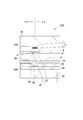
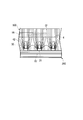
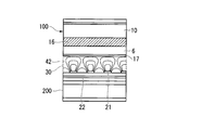
- FIG. 17 is a cross-sectional view schematically showing a liquid crystal display device using the FFS method.
- pixel electrodes 21 of a comb-like electrode and a common electrode 22 are usually array substrates with an insulating film interposed therebetween as electrodes for performing liquid crystal drive. It is formed on 200.
- Each of the pixel electrode 21 and the common electrode 12 is a transparent electrode formed of a material called ITO (Indium Tin Oxide) or the like so as not to reduce the aperture ratio of the pixel.
- ITO Indium Tin Oxide
- the liquid crystal molecules of the liquid crystal layer 30 are driven by a fringe electric field generated between the pixel electrode 21 and the common electrode 22.
- an insulating layer 6 is provided between the liquid crystal layer and the color filter 16.
- the equipotential lines 42 formed between the pixel electrode 21 and the common electrode 22 are shown in FIG. 17 because the color filter 16 and the like are insulators. And extends approximately perpendicular to the plane of the display substrate. If there is no large distortion in the shape of the equipotential line 42, the liquid crystal molecules aligned horizontally to the substrate surface of the liquid crystal layer 30 are uniformly parallel to the direction (horizontal direction) orthogonal to the thickness direction of the liquid crystal layer 30. It can be rotated to ensure high transmittance.
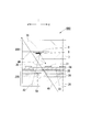
- FIG. 18 is a cross-sectional view schematically showing a liquid crystal display device using the FFS method.
- the color filter 16 is provided on the transparent substrate 10, the insulating layer 6 is provided on the color filter 16, and the insulation is provided.
- the transparent electrode 17 is provided on the layer 6, and the liquid crystal display device in which the liquid crystal layer 30 is located on the transparent electrode 17 is shown.
- FIG. 19 is a cross-sectional view schematically showing a liquid crystal display device using the FFS method.
- the transparent electrode 17 is provided on the transparent substrate 10, and the color filter 16 is provided on the transparent electrode 17.
- the insulating layer 6 is provided on the filter 16 and the liquid crystal layer 30 is positioned on the insulating layer 6.
- the transparent electrode 17 which is a conductive film.
- the transparent electrode 17 is provided at a position adjacent to the liquid crystal layer 30, the equipotential line is deformed in the liquid crystal layer 30, and the change of the operation or alignment state of the liquid crystal molecules becomes uneven. Accordingly, the liquid crystal molecules of the liquid crystal layer 30 are not aligned in the same direction, and the light transmittance is greatly reduced.
- the reason why the detection electrode 36 is disposed outside the liquid crystal layer 60 is that the detection electrode 36 which is a conductor is located near the liquid crystal layer 60. This is because the arrangement is likely to adversely affect the transmittance of the liquid crystal display device.
- the signal line (source line) of the active element (TFT) continuously sends the video signal to the active element during the display operation, noise accompanying the supply of the video signal is inevitably present around the source line. Occur. Therefore, for example, in FIGS. 3 to 6 of Patent Document 3, the wiring of the drive electrode 48 or the detection electrode is disposed in a mesh-like matrix overlapping the video signal line Px. A structure having overlapping pattern shapes is likely to pick up noise.
- paragraph [0033] of Patent Document 3 states that “time division can also be performed”, in touch sensing drive, it is not influenced by the liquid crystal drive frequency, and a frequency higher than liquid crystal drive. It is preferable to drive at high speed.
- TFT active element
- the drive signal may leak to the pixel not to be driven due to the light incidence or the off leak current, and the display image quality is easily deteriorated due to the crosstalk, flicker or the like.
- a display device provided with high definition pixels of 300 ppi (pixel per inch), and further 400 ppi or more, thinning of a black matrix or the like or wiring of an interconnection connected to an active element is required. For this reason, it is necessary to consider measures to prevent light incident on the TFT, increase in wiring resistance, and deterioration in image quality due to thinning of the connection lines of the black matrix or the active element.
- Patent Document 3 or Patent Document 4 little consideration is given to the problems caused by such high definition.
- the present invention has been made in view of the above problems, and it is difficult to pick up noise, reduce color mixing in which the color of the adjacent pixel is mixed with the color of the pixel to be driven, and secure the transmittance or display quality of the liquid crystal display To provide a liquid crystal display device and a display device substrate that can realize high definition pixels of 300 ppi or more.
- a liquid crystal display device comprises a first transparent substrate having a display area and a terminal area located outside the display area, and a first laminated structure of a black layer and a first metal layer.
- An active substrate having a transistor structure provided on a counter substrate having a wiring layer on the first surface of the first transparent substrate, a liquid crystal layer, a second transparent substrate, and the second transparent substrate and including a gate electrode
- An array substrate is provided, which has an element and a second wiring layer orthogonal to the first wiring layer, and is bonded to face the first surface of the first transparent substrate through the liquid crystal layer.
- a plurality of terminal portions having a laminated structure of the black layer and the first metal layer are provided in the terminal region, and the counter substrate is provided with the plurality of terminal portions.
- One black wiring layer, a black matrix having a plurality of openings formed in the display area, and a first transparent resin layer covering the black matrix are laminated in this order on the first surface, the black The matrix has a line width larger than the line width of the first wiring layer, and is overlapped so as to include the pattern of the first wiring layer in plan view, and the second wiring layer is a second metal.
- a light shielding pattern formed of the second metal layer, and the active element is covered with the light shielding pattern via a first insulating layer provided on the active element; Before the first wiring layer Performing a touch sensing by detecting a change in capacitance generated between the second wiring layer.
- the opening has a long side and a short side, and the second wiring layer is parallel to the short side of the opening in plan view. May be provided.
- the array substrate has a gate wiring electrically connected to the gate electrode, and the second wiring layer extends along the gate wiring in a plan view. It may be provided on the first insulating layer so as to extend in parallel.
- the potential of the second wiring layer may be a constant potential.
- the liquid crystal display device may include a color filter layer provided between the first metal layer and the first transparent resin layer.
- the first transparent resin layer may be provided between the black matrix and the liquid crystal layer.
- the dielectric constant of the black matrix may be in the range of 3.0 to 4.4.
- the active element includes a channel layer including two or more metal oxides composed of respective oxides of gallium, indium, zinc, tin and germanium. It may be a transistor.
- the array substrate includes a pixel electrode, a common electrode provided between the pixel electrode and the second transparent substrate, the pixel electrode and the common electrode. And a second insulating layer provided therebetween, the active element is electrically connected to the pixel electrode, and the liquid crystal layer is applied between the pixel electrode and the common electrode. It may be driven by a voltage.
- the initial alignment of the liquid crystal layer may be parallel to the surface of the second transparent substrate.
- the display device substrate is located on the first surface, the second surface opposite to the first surface, the display area, and the display area, and the first surface
- a transparent substrate having a terminal region provided in the wiring layer, a wiring layer provided on the first surface and having a laminated structure of a black layer and a metal layer having equal line widths, and provided in the terminal region, A plurality of terminal portions having a laminated structure of a black layer and the metal layer, and a plurality of openings provided so as to cover the wiring layer and formed in the display area, the wiring in a plan view
- a black matrix having a line width larger than the line width of the layer and overlapping so as to include the pattern of the wiring layer in the display area, and a first transparent resin layer covering the black matrix.
- the display device substrate according to the second aspect of the present invention may include a second transparent resin layer provided between the metal layer and the black matrix.
- the display device substrate is located on the first surface, the second surface opposite to the first surface, the display area, and the outside of the display area, and the first surface
- a transparent substrate having a terminal region provided in the wiring layer, a wiring layer provided on the first surface and having a laminated structure of a black layer and a metal layer having equal line widths, and provided in the terminal region, A plurality of terminal portions having a laminated structure of a black layer and the metal layer, and a plurality of openings provided so as to cover the wiring layer and formed in the display area, the wiring in a plan view
- a black matrix having a line width larger than that of a layer and overlapping so as to include the pattern of the wiring layer in the display area, and provided between the metal layer and the black matrix in the display area Color filters When, and a first transparent resin layer covering the black matrix.
- the display device substrate according to the third aspect of the present invention may include a second transparent resin layer provided between the color filter layer and the black matrix.
- the dielectric constant of the black matrix may be in the range of 3.0 to 4.4.
- a black layer is provided without using a member having a thickness such as a touch panel, high visibility is obtained, high definition can be achieved with 300 ppi or more, and high accuracy
- the distance between the first wiring layer and the second wiring layer in the above aspect of the present invention is the total thickness of the thickness of the liquid crystal layer and the thickness of the insulator such as the transparent resin layer provided in the liquid crystal cell. And is smaller than conventional liquid crystal display devices. For this reason, it is possible to obtain the effect of easily securing the capacitance. Since both the first wiring layer and the second wiring layer in the above aspect according to the present invention have a linear shape, it becomes difficult to pick up electrical noise as compared to a bent pattern or a mesh pattern, and the S / N ratio Can be improved.
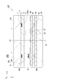
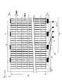
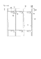
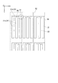
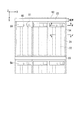
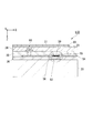
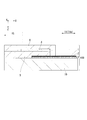
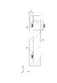
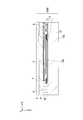
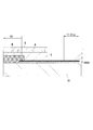
- FIG. 8 is a cross-sectional view partially showing the liquid crystal display device according to the first embodiment of the present invention, and a cross-sectional view taken along the line A-A ′ shown in FIG. 7. It is the top view seen from the surface of the transparent substrate of the display apparatus substrate comprised to the liquid crystal display device which concerns on 1st Embodiment of this invention. It is a top view which shows an example of the 1st wiring layer comprised in the liquid crystal display device concerning a 1st embodiment of the present invention, and the 2nd wiring layer.
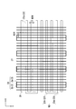
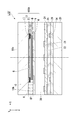
- FIG. 8 is a plan view partially showing a display device substrate of the liquid crystal display device according to the first embodiment of the present invention, which is a partially enlarged plan view of the liquid crystal display device shown in FIG.
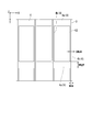
- FIG. 5 is a plan view partially enlarging the array substrate included in the liquid crystal display device according to the first embodiment of the present invention, showing an example of the positional relationship between active elements, gate wires, and source wires, The opening part of the array substrate matched with the position of the opening part of the black matrix provided on the display apparatus substrate which shows is shown.
- FIG. 6 is a partially enlarged plan view of the array substrate included in the liquid crystal display device according to the first embodiment of the present invention, showing a structure in which pixel electrodes are stacked on the opening of the array substrate shown in FIG. 5.
- FIG. 5 is a plan view partially enlarging the array substrate included in the liquid crystal display device according to the first embodiment of the present invention, showing an example of the positional relationship between active elements, gate wires, and source wires, The opening part of the array substrate matched with the position of the opening part of the black matrix provided on the display apparatus substrate which shows is shown.
- FIG. 6 is a partially enlarged plan view of the array substrate included in the liquid
- FIG. 8 is a cross-sectional view partially showing the array substrate included in the liquid crystal display device according to the first embodiment of the present invention, and a cross-sectional view taken along the line B-B 'shown in FIG. 7;
- FIG. 3 is a cross-sectional view partially showing a display device substrate included in the liquid crystal display device according to the first embodiment of the present invention, and a cross-sectional view taken along line C-C ′ shown in FIG.
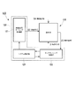
- FIG. 1 is a block diagram of a liquid crystal display device according to an embodiment of the present invention. It is a schematic cross section for demonstrating the effect obtained by the black matrix comprised to the board
- the liquid crystal display using a FFS method it is a schematic cross section for demonstrating the malfunction when a transparent electrode (electrically conductive film) is comprised between a color filter and a liquid crystal layer.
- the liquid crystal display using a FFS method it is a schematic cross section for demonstrating the malfunction when a transparent electrode (conductive film) is comprised between a color filter and a transparent substrate.
- the display device substrate according to the present embodiment is a display other than a liquid crystal display device such as an organic EL display device. It is applicable also to an apparatus.
- both or one of the first wiring layer and the second wiring layer, which are wirings for touch sensing may be referred to as a touch sensing wiring or a touch sensing electrode.
- the liquid crystal display device described in the present embodiment includes the display device substrate according to the present invention. Further, the “plan view” described below means a plane viewed from the direction in which the observer observes the display surface of the liquid crystal display device (the plane of the display device substrate).
- the shape of the display unit of the liquid crystal display device according to the embodiment of the present invention, the shape of the opening defining the pixels, and the number of pixels constituting the liquid crystal display device are not limited.
- the planar view, the direction of the short side of the pixel is defined as the X direction, the direction of the long side is defined as the Y direction, and the thickness direction of the transparent substrate is the Z direction.
- the liquid crystal display device will be described.
- the X direction and the Y direction defined as described above may be interchanged to constitute a liquid crystal display device.
- FIG. 1 is a cross-sectional view partially showing a liquid crystal display device LCD according to the present embodiment.
- the liquid crystal display device LCD according to the first embodiment of the present invention comprises a display device substrate 100 (opposite substrate), an array substrate 200 bonded to the display device substrate 100 to face each other, a display device substrate 100 and an array And a liquid crystal layer 30 sandwiched by the substrate 200.
- a backlight unit for supplying light to the inside of the liquid crystal display device LCD is provided on the back surface (the opposite surface to the surface of the array substrate 200 on which the liquid crystal layer 30 is disposed) of the array substrate 200 constituting the liquid crystal display device LCD. There is.
- the backlight unit may be provided on the side surface of the liquid crystal display device LCD.
- a reflection plate, a light guide plate, a light diffusion plate or the like that reflects light emitted from the backlight unit toward the inside to the liquid crystal display device LCD is provided on the back surface of the array substrate 200.
- an alignment film for giving an initial alignment to the liquid crystal layer 30 an optical film such as a polarizing film, a cover glass for protection, and the like are omitted.
- the display device substrate 100 (counter substrate) includes a transparent substrate 10 (first transparent substrate) having a first surface 10 b and a second surface 10 a on the opposite side to the first surface 10 b.
- the second surface 10 a is a surface exposed toward the outside of the liquid crystal display device LCD, and functions as a touch sensing input surface.
- the first surface 10 b is a surface facing the array substrate 200.
- the display device substrate 100 includes a first wiring layer 3 formed on the first surface 10 b of the transparent substrate 10 and a transparent resin layer 5 formed on the transparent substrate 10 so as to cover the first wiring layer 3 (first 2) transparent resin layer), black matrix 4 formed on transparent resin layer 5, and transparent resin layer 6 (first transparent resin layer) formed on transparent resin layer 5 so as to cover black matrix 4 Prepare.
- the transparent resin layer 6 is provided between the black matrix 4 and the liquid crystal layer 30. That is, in the display device substrate 100, the first wiring layer 3, the black matrix 4, and the transparent resin layer 6 are stacked in this order on the first surface 10b.
- a transparent resin layer 5 is provided between the first metal layer 2 and the black matrix 4.
- the first wiring layer 3 (wiring layer) is formed by the black layer 1 formed on the first surface 10 b of the transparent substrate 10 and the first metal layer 2 (conductive layer, metal layer) formed on the black layer 1. It has the laminated structure comprised. As shown in FIG. 1 or 2, the line width of the first wiring layer 3 can be made the same as the line width of the black layer 1 and the first metal layer 2 which are components of the first wiring layer 3. The line widths of the black layer 1 and the first metal layer 2 may be different from each other. For example, the line width of the black layer 1 may be wider than the line width of the first metal layer 2. From the viewpoint of improving the aperture ratio of the pixel, the line width of the black layer 1 and the line width of the first metal layer 2 are desirably the same.
- the first metal layer 2 can be formed of one or more metal thin films. In the configuration in which the first metal layer 2 is formed of a metal thin film, incidence of light on the active element 51 (described later) can be suppressed.
- the transparent substrate 10 includes an effective display area 15 (display area), a terminal area 11a located on the first surface 10b and located outside the effective display area 15, and frame portions Fx and Fy. And.
- the terminal area 11a is provided with a plurality of terminal portions 11 as described later.
- the frame portions Fx and Fy are provided on the first surface 10 b of the transparent substrate 10 so as to surround the effective display area 15.
- a light shielding thin film pattern may be disposed in the frame portions Fx and Fy in order to completely block the light emitted from the backlight unit.
- the first metal layer 2 may be formed using the same metal thin film used for forming the first metal layer 2 or the light shielding layer 59 (described later).
- the light shielding thin film patterns are formed in the frame portions Fx and Fy so as to be electrically independent from each other.
- a black matrix 4 having a plurality of formed openings 12 is provided in the effective display area 15.
- the first wiring layer 3 disposed on the display device substrate 100 and the second wiring layer 23 (described later) disposed on the array substrate 200 will be described with reference to FIGS. 2 and 3. In FIG. 3, only the first wiring layer 3 and the second wiring layer 23 are extracted and described in order to facilitate understanding of the positional relationship between the first wiring layer 3 and the second wiring layer 23. .
- the first wiring layer 3 disposed on the display device substrate 100 is orthogonal to the second wiring layer 23 (described later) disposed on the array substrate 200 in a plan view.
- the first wiring layer 3 and the second wiring layer 23 function as touch sensing electrodes for detecting a pointer such as a finger approaching the second surface 10 a of the display device substrate 100 from the outside of the liquid crystal display device LCD.
- the three first wirings 3a are electrically connected to each other by the connection wiring 3b (3).
- the connection wiring 3 b extends in the X direction.
- the first wiring 3a extends in the Y direction.
- One first wiring group G1 is formed by the connection wiring 3b and the three first wirings 3a.
- one first wiring group G1 is electrically connected to one terminal portion 11 via the wiring 3c.
- the plurality of first wiring groups G1 are provided on the first surface 10b of the transparent substrate 10 at equal intervals along the X direction. Furthermore, the plurality of terminal portions 11 of the number corresponding to the number of the plurality of first wiring groups G1 are provided in the terminal region 11a at equal intervals along the X direction.
- the display device substrate 100 is provided with a floating pattern 27 extending in the Y direction in parallel with the first wiring 3a.
- the floating pattern 27 is simultaneously formed on the transparent substrate 10 when the first wiring layer 3 is formed, and has the same layered structure as the first wiring layer 3.
- the floating pattern 27 is an electrically floating conductive pattern and is not electrically connected to the first wiring layer 3.
- the three second wirings 23a are electrically connected to each other by the connection wiring 23b (23).
- the connection wiring 23 b extends in the Y direction.
- the second wiring 23a extends in the X direction.
- One second wiring group G2 is formed by the connection wiring 23b and the three second wirings 23a.
- One second wiring group G2 is connected to a terminal provided on the array substrate 200.
- a plurality of terminal portions are provided on the array substrate 200 in a number corresponding to the number of the plurality of second wiring groups G2.
- the array substrate 200 is provided with a floating pattern 28 extending in the X direction in parallel with the second wiring 23 a.
- the floating pattern 28 is simultaneously formed on the transparent substrate 20 when the second wiring layer 23 is formed, and has the same structure as the second wiring layer 23.
- the floating pattern 28 is an electrically floating conductive pattern and is not electrically connected to the second wiring layer 23.
- the plurality of first wirings 3a (3) constituting the first wiring layer 3 and the plurality of second wirings 23a (23) constituting the second wiring layer 23 intersect at a plurality of intersections.
- Touch sensing drive is performed by detecting such a change in capacitance (described later).
- the line width M2W of the second wiring layer 23 (second wiring 23a) is set to the first wiring layer 3 (first The fringe capacitance (electrostatic capacitance) generated between the first wiring layer 3 and the second wiring layer 23 can be increased by making the line width M1W of the first wiring 3a larger. Furthermore, by forming the second wiring layer 23 on the gate wiring 52 (described later), the width of the second wiring layer 23 can be expanded.
- the first wiring layer 3 and the second wiring layer 23 be covered by the black matrix 4 in plan view. That is, the line width of the first wiring layer 3 and the line width of the second wiring layer 23 are preferably smaller than the line width of the black matrix 4.
- the line width BMsW of the black matrix 4 (second light shielding portion 4 b) is larger than the line width M1W of the first wiring layer 3, and the black matrix 4 (first light shielding portion The line width BMgW of 4a) is larger than the line width M2W of the second wiring layer 23 (second line 23a). That is, the black matrix 4 overlaps the first wiring layer 3 so as to include the pattern (first wiring pattern) of the first wiring layer 3 in plan view.
- the reason for defining the line width in this way is that it arises from the first wiring layer 3 or the second wiring layer 23 when each of the first wiring layer 3 and the second wiring layer 23 is formed using a metal thin film or the like. This is to prevent the reflected light from entering the eye of the observer or the channel layer 50 of the active element 51.
- sandwiching the thin metal line (first metal layer 2) having high light reflectivity between the black layer 1 and the black matrix 4 the visibility of the liquid crystal display or the display image quality can be greatly improved.
- the number of first wirings 3a constituting the first wiring layer 3, the number of second wirings 23a constituting the second wiring layer 23, the plurality of first wirings 3a are one.
- the number of groups for example, three first wires 3a electrically connected to one another are combined to form one group, and a plurality of groups are provided), a plurality of second wires 23a (Eg, three second wires 23a electrically connected to each other form one group, and a plurality of groups are provided),
- Method of forming the wiring layer group driving method such as thinning driving (driving the selected wiring without driving all the wiring layers), width of the first wiring 3a, width of the second wiring 23a, floating putter 27 and 28 the number of, width, etc. of the floating pattern 27 and 28 is not limited.
- the signal supply is not performed in the twelve first wires 3a, and the signal detection is not performed either.
- the remaining six may form a plurality of groups in which one group is defined (grouping).
- 12 out of the 18 second wirings 23 a constituting the second wiring layer 23 are excluded (12 signals are not supplied in the 12 second wirings 23 a except for the 12 second wirings 23 a, and signal detection is not performed either.
- the remaining six may form a plurality of groups in which one group is defined (grouping).
- touch sensing drive or drive signal detection can be performed using the first wiring 3a and the second wiring 23a thus grouped, and the speed of touch sensing can be increased.
- FIG. 3 a configuration example in which one group is formed by three first wirings 3a and one group is formed by three second wirings 23a is illustrated.
- FIG. 4 is a partially enlarged plan view of the plan view of the display device substrate 100 shown in FIG. 2 and is a view for explaining the relationship between the black matrix 4 and the first wiring layer 3.
- FIG. 4 shows the pixel configuration of the display device substrate 100 bonded to the array substrate 200.
- the black matrix 4 has a first light shielding portion 4 a extending in the X direction and a second light shielding portion 4 b extending in the Y direction.
- the first light shielding portion 4a and the second light shielding portion 4b cross each other, and the black matrix 4 has an opening 12 surrounded by the first light shielding portion 4a and the second light shielding portion 4b.
- the first light shielding portion 4 a forms the short side of the opening 12, and the second light shielding portion 4 b forms the long side of the opening 12.
- the length of the opening 12 in the Y direction (long side) is larger than the length in the X direction (short side), but the length of the opening 12 in the X direction is Y direction It may be larger than the length.
- the black matrix 4 is provided with a plurality of openings 12 whose number corresponds to the number of the plurality of pixels constituting the display surface of the liquid crystal display device LCD.
- the plurality of openings 12 are arranged in the effective display area 15 along the X direction and the Y direction, that is, provided in a matrix.
- the first light shielding portion 4 a extends so as to overlap the gate wiring 52 (described later) in plan view, and has a line width BMgW (width along the Y direction).
- the second light shielding portion 4 b extends so as to overlap the source wiring 54 (described later) in plan view, and has a line width BMsW (a width along the X direction).
- the second light shielding portion 4 b of the black matrix 4 overlaps the first wiring layer 3
- the line width BMsW of the second light shielding portion 4 b is the first wiring layer It is larger than the line width M1W of 3.
- the center position of the line width M1W of the first wiring layer 3 and the center position of the line width BMsW of the second light shielding portion 4b of the black matrix 4 coincide with the center line CW. Further, as shown in FIG. 1, the first wiring layer 3 and the second light shielding portion 4b are provided on the side of the pixel (for example, at the position overlapping the source wiring 54), and the pixel center CL in one pixel Are arranged in line symmetry with respect to.
- the first metal layer 2 constituting the first wiring layer 3 As a material of the first metal layer 2 constituting the first wiring layer 3, copper, silver, gold, titanium, molybdenum, aluminum, or an alloy containing these metals can be applied. Since nickel is a ferromagnetic material, the film forming rate is low in the step of forming the first metal layer 2 using nickel. As a method of forming the first metal layer 2 using nickel, a vacuum film forming method such as sputtering can be employed. When the color filter is not formed in the manufacturing process of the display device substrate 100 and the like, the first metal layer 2 can be formed using aluminum and an aluminum alloy. Chromium has a negative problem of environmental pollution or a large resistance value, but can be used as a base film of the first metal layer 2 in order to improve adhesion.
- a metal oxide containing indium oxide can be applied as an underlayer or surface layer of the first metal layer 2.
- copper or aluminum, magnesium, calcium, beryllium, scandium, gallium, yttrium, titanium, molybdenum, indium, tin or the like may be further added to the above metals or alloys.
- An alloy added with one or more metal elements selected from zinc, neodymium, nickel and aluminum can be applied.
- the first metal layer 2 may be composed of a plurality of metal layers.
- the first metal layer 2 When a copper alloy thin film or an aluminum alloy thin film is employed as the first metal layer 2, when the film thickness is 100 nm or more or 150 nm or more, visible light hardly transmits. Therefore, the first metal layer 2 can obtain a sufficient light shielding property with a film thickness of, for example, 100 nm to 300 nm.
- the first metal layer 2 may be composed of a three-layer structure of indium copper alloy / magnesium copper alloy / indium copper alloy, and may each have a film thickness of 10 nm / 120 nm / 15 nm. In this case, for example, the addition amount of indium to copper is 18 at%, and the addition amount of magnesium to copper is 0.5 at%. The method of forming the first metal layer 2 will be described.
- the transparent substrate 10 and the first metal layer 2 When film formation is performed on the interface or the interface between the base film and the first metal layer 2, oxygen gas can be introduced to form the first metal layer 2.
- a vacuum film forming apparatus such as a sputtering apparatus can be used.
- a metal layer containing a large amount of oxygen and having a film thickness of about 2 nm to 30 nm may be formed on the surface or interface of the first metal layer 2.
- the black layer 1 which comprises the 1st wiring layer 3
- carbon or a carbon nanotube which functions as a light absorptive coloring material can be used, for example.
- a plurality of organic pigments may be further added to the black layer 1 for color adjustment.
- the optical density of the black layer 1 obtained by transmission measurement can be, for example, less than 2.
- the optical density of the black layer 1 obtained by transmission measurement is in the range of 0.4 to 1.8 per 1 ⁇ m unit film thickness, and the film thickness of the black layer 1 is 0.1 ⁇ m to 0.7 ⁇ m. It is preferably in the range.
- the reflectance of light generated at the interface between the transparent substrate 10 and the black layer 1 is 3%. It may exceed.
- the optical density of the black layer 1, the reflection color, or the reflectance at the interface between the transparent substrate 10 and the black layer 1 may be appropriately selected from black coloring materials such as carbon, or a plurality of organic substances added to carbon It can be set appropriately by adjusting the amount of pigment or resin.
- the reflectance at the interface between the transparent substrate 10 and the black layer 1 can be 3% or less in the visible light range of 400 nm to 700 nm.
- a photosensitive black coating solution is applied to the transparent substrate 10 (first surface 10 b).
- the black coating solution applied on the transparent substrate 10 is exposed to form a patterned black layer 1.
- a development step, a heat treatment step and the like are performed to obtain a hardened black layer 1.
- the black coating solution is produced, for example, by dispersing carbon in a coating solution in which an organic solvent, a photocrosslinkable acrylic resin, and an initiator are mixed.
- the formation method of the black layer 1 is not limited to the method mentioned above. Next, another method of forming the black layer 1 will be described.
- a black coating solution is applied on the transparent substrate 10 to form a black film.
- a metal thin film containing a material for forming the first metal layer 2 is formed on the black film using the above-described film forming method and film forming apparatus.
- the first metal layer 2 is formed by patterning the metal thin film by a wet etching method. As a result, the patterned first metal layer 2 is formed on the black film, and the black film is partially exposed between the first metal layers 2.
- the black layer 1 is patterned by dry etching the underlying black film.
- the line width of the first metal layer 2 and the line width of the black layer 1 can be made substantially equal, and can be processed into a high definition pattern.
- an organic solvent in which a photosensitive resin such as acrylic or a thermosetting resin is dispersed with a curing agent, an initiator, a monomer, a dispersing agent or the like and the above-mentioned carbon or organic pigment is used.
- the reflectance of the interface between the transparent substrate 10 and the black layer 1 can be lowered by applying a resin with a low refractive index to the black coating solution.
- FIG. 9 is a cross-sectional view taken along the line CC ′ shown in FIG. 2, and shows a cross-sectional structure of the terminal portion 11 formed in the terminal region 11a (outside of the effective display region 15).
- the terminal portion 11 Similar to the first metal layer 2 and the black layer 1 constituting the first wiring layer 3, the terminal portion 11 has a laminated structure (two layers) of the first metal layer 2 and the black layer 1. Outside the effective display area 15, the transparent resin layer 6 covers the black matrix 4 with the end and the end of the transparent resin layer 5, and the first metal layer 2 constituting the terminal 11 is used as a terminal area 11 a. Exposed to As shown in FIG. 2, a plurality of terminal portions 11 are arranged along the X direction.
- the terminal portion 11 is used for electrical mounting. Since such a terminal portion 11 is provided on the display device substrate 100, in a structure in which the display device substrate 100 is incorporated in the liquid crystal display device LCD, the touch sensing control portion 122 (described later) passes through the terminal portion 11. A drive signal can be supplied to the first wiring group G1, and the touch sensing control unit 122 can detect a detection signal output from the first wiring group G1 through the terminal unit 11.
- the relative dielectric constant of the black matrix 4 is preferably in the range of 3.0 to 4.4.
- the reason why the relative permittivity of the black matrix 4 is preferably in the range of 3.0 to 4.4 will be described below.
- a fringe electric field formed between the comb-tooth-shaped pixel electrode 21 and the common electrode 22 located below the pixel electrode 21 To drive it is desirable that the equipotential lines in the fringe electric field be formed uniformly in the direction from the liquid crystal layer 30 to the color filter 16.
- a black film in which carbon, which is frequently used as a black color material of a black matrix, is dispersed has an extremely high dielectric constant of approximately 10 to 20.
- a black matrix having a high relative dielectric constant greatly affects the liquid crystal driving.
- a low dielectric constant black matrix in the range of 3.0 to 4.4.
- the measurement of the relative dielectric constant is performed at a frequency of 60 Hz to 480 Hz, which is a driving frequency of the liquid crystal, using a measuring instrument such as an impedance analyzer.
- a colored film including a black film
- a transparent resin such as acrylic as a base material
- a black film or a colored film having a certain amount of coloring material or pigment in order to ensure effective light shielding or coloring properties Need to be distributed.
- the lower limit value of the relative dielectric constant considering the amount of the pigment dispersed in the colored film is 3.0.
- ⁇ is slightly higher, for example, 4.5 to 6.5.
- a liquid crystal selected from the range of anisotropy and having a selected dielectric anisotropy is applied to the present embodiment. This provides several benefits. Specifically, there is an advantage that the threshold voltage related to the liquid crystal drive can be lowered and the response (rise) of the liquid crystal can be improved.
- the value of the relative dielectric constant of the display device substrate or the color filter component can be made smaller than the value of the relative dielectric constant of the liquid crystal to obtain conditions that do not affect the liquid crystal driving. be able to.
- a light-shielding film of a mixed color material in which a plurality of organic pigments are combined is used as the black matrix 4 or a light-shielding film in which a small amount of carbon of 10% or less in color material solid ratio is added to the plurality of pigments
- the dielectric constant of the black matrix 4 can be set to 4.4 or less. It is also preferable to use a resin with a low refractive index as a resin used as a dispersion matrix of the black matrix 4.
- the black matrix 4 (second light shielding portion 4b) is provided between two pixels adjacent to each other. Specifically, the black matrix 4 is disposed to face a boundary area located between the first pixel located at the center of FIG. 1 and the second pixel located to the left of the first pixel. In other words, the black matrix 4 is provided to face the boundary area located between the pixel electrode 21 constituting the first pixel and the pixel electrode 21 constituting the second pixel. A liquid crystal layer 30 is present between the display device substrate 100 and the array substrate 200 in this boundary region. Further, the boundary area corresponds to an alignment failure area indicated by reference numeral 40 in FIG. 14 described later. Similarly, the first light shielding portion 4a of the black matrix 4 is provided to face a boundary area located between two adjacent pixels.
- the array substrate 200 is bonded so as to face the first surface 10 b of the transparent substrate 10 via the liquid crystal layer 30.
- the array substrate 200 is formed on the transparent substrate 20 so as to cover the transparent substrate 20 (second transparent substrate), the gate wiring 52 and the gate electrode 53 formed on the transparent substrate 20, and the gate wiring 52 and the gate electrode 53.
- a first insulating layer 24 formed on the substrate 25 and a pixel electrode 21 formed on the first insulating layer 24 are provided.
- an active element 51 TFT, described later
- TFT having a transistor structure including a source wiring 54, a source electrode 55, a drain electrode 56, and a channel layer 50 is provided.
- FIG. 5 is a plan view showing the structure before forming the pixel electrode 21 on the array substrate 200, and shows the active element 51, the source wiring 54, the gate wiring 52, the drain electrode 56, the contact hole 60, the common electrode 22 and so on. It is a figure explaining a positional relationship.
- FIG. 6 is a plan view showing the structure after forming the pixel electrode 21 connected to the drain electrode 56 through the contact hole 60, and shows the structure before forming the second wiring layer 23 and the light shielding layer 59.
- FIG. FIG. 7 is a plan view showing the structure after the second wiring layer 23 and the light shielding layer 59 are formed.
- FIG. 8 is a cross-sectional view taken along the line B-B 'shown in FIG.
- the common electrode 22 is disposed in the opening 12 of the pixel.
- the active element 51 is provided at a position where the gate electrode 53 extending in the Y direction from the gate wiring 52 and the source electrode 55 extending in the X direction from the source wiring 54 overlap. In the example shown in FIG. 5, it is located at the upper right corner of the pixel.
- the active element 51 includes a drain electrode 56 electrically connected to the pixel electrode 21 through the contact hole 60, a source electrode 55 electrically connected to the source wiring 54, and a drain electrode.
- a channel layer 50 provided so as to partially overlap both the electrodes 55, 56 between the source electrode 55 and the source electrode 55, and a gate disposed so as to face the channel layer 50 via the third insulating layer 26.
- an electrode 53 The source wires 54 are arranged in parallel in the Y direction, and the gate wires 52 are arranged in parallel in the X direction.
- the gate wiring 52 (gate electrode 53) is directly formed on the transparent substrate 20.
- an insulating layer is formed in advance on the transparent substrate 20, and the gate wiring 52 (gate) is formed on this insulating layer.
- An electrode 53) may be formed.
- an electric field is generated between the channel layer 50 and the gate electrode 53 (field effect) in accordance with a signal supplied to the gate electrode 53, and the switching operation of the transistor is performed.
- the pixel electrode 21 is provided to face the common electrode 22 via the first insulating layer 24.
- the pixel electrode 21 is formed of ITO, which is a mixed oxide of indium oxide or tin oxide.
- the pixel electrode 21 is provided to correspond to each of the plurality of openings 12 arranged in a matrix, and is formed in a comb shape (see FIG. 6).
- the pixel electrode 21 includes three comb electrode portions 21a and an electrode base 21b.
- the electrode base 21 b extends in the X direction, is provided at a position overlapping the contact hole 60, and is electrically connected to the drain electrode 56 via the contact hole 60.
- the three comb-tooth electrodes 21a extend in the Y direction from the electrode base 21b. Between the comb-tooth electrode portions 21a adjacent to each other, as shown in FIG. 1, the first insulating layer 24 is exposed to the liquid crystal layer 30 (the alignment film is omitted), and the active element 51 is driven. Transverse electric field is generated.
- the second wiring layer 23 and the light shielding layer 59 are arranged side by side.
- the second wiring layer 23 (second wiring pattern) is provided at a position corresponding to the gate wiring 52 (a position overlapping the gate wiring 52), and above the gate wiring 52.
- the second wiring layer 23 has a line width M2W, and extends parallel to the short side of the opening 12 along the gate wiring 52 (parallel to the X direction).
- the light shielding layer 59 is provided at a position corresponding to the active element 51 and is formed to cover the active element 51 via the first insulating layer 24 as shown in FIG. Further, as shown in FIGS. 6 and 7, the light shielding layer 59 is formed to cover the electrode base 21 b of the pixel electrode 21.
- the light shielding layer 59 is formed using a metal which is the same material as the material of the second wiring layer 23.
- the light shielding layer 59 extends in the X direction in parallel to the second wiring layer 23.
- the light shielding layer 59 and the second wiring layer 23 are formed using the same metal layer in the same formation process.
- a well-known patterning technique is used as a formation method.
- As a material for forming the second wiring layer 23 and the light shielding layer 59 an aluminum alloy (second metal layer) containing neodymium is used.
- the light shielding layer 59 and the second wiring layer 23 may form the same layer in position. That is, the second wiring layer 23 is formed of the second metal layer and has a light shielding pattern (light shielding layer 59) formed of the second metal layer.
- the light shielding pattern covers the active element 51 via the first insulating layer 24.
- the light shielding layer 59 and the second wiring layer 23 may be electrically connected, but in this case, it is easy to pick up noise. Therefore, it is preferable that the light shielding layer 59 and the second wiring layer 23 be separated from each other and electrically insulated.
- the light shielding layer 59 may be located directly above the first insulating layer 24 and directly on the pixel electrode 21 (electrode base 21 b). Alternatively, the light shielding layer 59 may be formed on the first insulating layer 24 and below the pixel electrode 21 (electrode base 21 b). In the present embodiment, as an example, a structure in which a light shielding layer 59 is provided on the pixel electrode 21 is shown in FIG.
- the planar pattern of the light shielding layer 59 is appropriately determined in accordance with the portion where the light incidence needs to be prevented.
- the light shielding layer 59 according to the embodiment of the present invention can be formed simultaneously with the second wiring layer 23 using the same metal layer as the second wiring layer 23, and a light shielding pattern for the purpose of light shielding. Has the advantage of being free to design.
- the second wiring layer 23 which is one of the touch sensing wirings above the source wiring 54 without providing the second wiring layer 23 above the gate wiring 52.
- the second wiring layer 23 easily picks up noise caused by the video signal.
- the number or thickness of the insulating layers provided on the transparent substrate 20 may be increased.
- An insulating layer may be separately formed on the upper surface or the lower surface of the second wiring layer 23 and the upper surface or the lower surface of the light shielding layer 59.
- the insulating layer provided to be in contact with the surfaces of the second wiring layer 23 and the light shielding layer 59 is an inorganic insulating layer called SOG (Spin On Glass) or an organic insulating layer such as an acrylic resin. May be In this case, the inorganic insulating layer or the organic insulating layer is laminated on the first insulating layer 24 prior to the formation of the second wiring layer 23.
- SOG Spin On Glass
- organic insulating layer such as an acrylic resin
- the gate interconnection 52 and the source interconnection 54 are metal interconnections formed of a two-layer structure of copper alloy and titanium. In such a two-layer structure of metal wiring, a copper alloy is located in the upper layer.
- the channel layer 50 is formed of an InGaZnO-based oxide semiconductor.
- embodiments of the present invention do not limit the materials that make up the above structure.
- the various materials described above may be used as the metal or alloy material constituting the touch sensing wiring.
- the structure of the touch sensing wiring is not limited to a single layer structure, and a multilayer structure in which metal oxides are stacked can be employed as a plurality of metal layers.
- the channel layer 50 of the active element 51 can be formed of a silicon-based semiconductor such as polysilicon or an oxide semiconductor.
- the channel layer 50 is preferably an oxide semiconductor including two or more metal oxides of gallium, indium, zinc, tin, and germanium, such as IGZO (registered trademark).
- the channel layer 50 is formed of an InGaZnO-based metal oxide.
- the active element 51 using an oxide semiconductor such as IGZO for the channel layer 50 has a high electron mobility, and can apply a necessary driving voltage to the pixel electrode 21 in a short time of 2 msec (milliseconds) or less, for example.
- one frame in double-speed driving (when the number of display frames per second is 120) is about 8.3 msec.
- the remaining approximately 6 msec obtained by subtracting 2 msec of liquid crystal driving can be allocated to touch sensing driving.
- the active element 51 using an oxide semiconductor for the channel layer 50 has a small leak current as described above, the drive voltage applied to the pixel electrode 21 can be held for a long time.
- touch sensing driving and liquid crystal driving are time division, for example, signal lines, scanning lines, storage capacitance lines, etc. of active elements are formed of copper wiring having a smaller wiring resistance than aluminum wiring, and furthermore, channels of active elements As a material of the layer 50, IGZO which can be driven in a short time can be used. In this case, in scanning in touch sensing driving, a temporal margin is expanded, and a change in generated capacitance can be detected with high accuracy.
- the driving time of a liquid crystal or the like can be shortened, and in the video signal processing of the entire display screen, sufficient time can be provided for applying to touch sensing.
- the active element 51 using an oxide semiconductor for the channel layer 50 has almost no electrical leakage of the active element 51 at the time of image display, and achieves touch display in parallel with liquid crystal drive while securing stable image display. It becomes possible to drive.
- the needs or interfaces for touch sensing are diversified, and for example, high accuracy is required in order to realize personal authentication or input with a fine pen tip for detecting and detecting a fingerprint or the like. .
- the active element 51 using an oxide semiconductor for the channel layer 50 has a higher electrical withstand voltage than a silicon-based semiconductor, and is suitable for such a high amplitude.
- a thin film transistor using an oxide semiconductor as the channel layer 50 has, for example, a bottom gate structure.
- a top gate type or a double gate type transistor structure may be used for the thin film transistor.
- the channel layer of the thin film transistor faces the surface of the array substrate close to the backlight unit. In this configuration, the light of the backlight unit is easily incident on the channel layer, which is a disadvantageous structure.
- the second wiring layer 23 simultaneously formed as the same metal layer as the light shielding layer 59 is also located in the lowermost layer. That is, the distance between the second wiring layer 23 and the first wiring layer 3 in the thickness direction of the array substrate 200 becomes long. For this reason, there is a concern about the influence on touch sensing, such as an increase in electrical noise.
- a thin film transistor provided with a channel layer of an oxide semiconductor may be employed as an active element constituting an optical sensor or other active element. Since the active element having such a structure has high memory performance (less leak current), it is easy to maintain the pixel capacitance after applying the liquid crystal drive voltage.
- a driver circuit for controlling liquid crystal driving or touch driving may be formed on the transparent substrate 20 at a position corresponding to the frame portions Fx and Fy provided outside the effective display area 15.
- the active element constituting the driver circuit may include a channel layer 50 formed of an oxide semiconductor such as IGZO.
- the liquid crystal layer 30 is disposed between the display device substrate 100 and the array substrate 200 which are bonded to face each other.
- the liquid crystal molecules of the liquid crystal layer 30 are driven by a fringe electric field generated between the pixel electrode 21 and the common electrode 22 with the switching operation of the active element 51.
- the liquid crystal has positive dielectric anisotropy, and the initial alignment of the liquid crystal is horizontal alignment.
- the direction of the alignment treatment by rubbing or photoalignment is, for example, 5 ° to 20 ° with respect to the alignment direction of the comb-like pixel electrodes in plan view in the case of liquid crystal with positive dielectric anisotropy. It may be done in the inclined direction.
- FIG. 14 is a block diagram of a liquid crystal display device LCD according to the present embodiment.
- FIG. 14 is a block diagram for explaining the function of the liquid crystal display device according to the present embodiment.
- the liquid crystal display device LCD according to the present embodiment includes a display unit 110 provided at a position corresponding to the effective display area 15, a display unit 110, and a control unit 120 for controlling a touch sensing function.
- the control unit 120 has a known configuration, and includes a video signal timing control unit 121, a touch sensing control unit 122, and a system control unit 123.
- the control unit 120 controls liquid crystal driving and touch sensing driving.
- the system control unit 123 controls the video signal timing control unit 121 and the touch sensing control unit 122. Further, in the liquid crystal display device LCD, for example, an LED light emitting element that emits red light, green light, blue light and the like is used as a light source of the backlight unit.
- the control unit 120 controls color display by a field sequential method.
- the first wiring layer 3 and the second wiring layer 23 may be provided between any one of the first wiring layer 3 and the second wiring layer 23 and the common electrode 22. Control may be performed to apply a voltage different from the liquid crystal drive voltage between each of the above and the common electrode. According to this control method, it is possible to assist liquid crystal drive such as speeding up or turning on (off) of liquid crystal molecules or control of alignment.
- the liquid crystal drive and the touch sensing drive may not be time-divisionally driven.
- the second wiring layer 23 can be used as a detection electrode of constant potential
- the first wiring layer 3 can be used as a drive electrode of touch sensing.
- the degree of interference of the touch sensing drive with the liquid crystal drive is reduced, and the drive frequency of the pixel electrode for driving the liquid crystal and the drive frequency of the touch sensing electrode can be made different.
- the potential of the second wiring layer 23 can be made constant.
- the control unit 120 may have a function of detecting an external noise frequency, and an adjusting function of adjusting a band of a touch sensing drive frequency so as to be different from the detected external noise frequency.
- the drive frequency of touch sensing can be several kilohertz to several tens kilohertz
- the frequency of liquid crystal drive can be 60 Hz to 480 Hz.
- touch sensing drive and liquid crystal drive can be time-shared.
- the frequency of the scan signal for detecting the capacitance is arbitrarily adjusted in accordance with the required speed of touch input.
- the drive frequency of touch sensing is desirably higher than the liquid crystal drive frequency as described above.
- the second wiring layer 23 may function as a driving electrode and the first wiring layer 3 may function as a detection electrode.
- the second wiring layer 23 is a drive electrode (scan electrode) which applies an alternating current pulse at a constant frequency.
- a voltage (AC signal) applied to the drive electrode may be an inversion drive method in which positive and negative voltages are inverted.
- a dot inversion driving method may be used in which the pixel electrode is driven for each pixel.
- the influence of the touch sensing drive voltage on the liquid crystal display can be reduced by reducing the voltage width (peak to peak) of the AC signal to be applied regarding the touch sensing drive voltage.
- the potential (voltage) set as a constant potential is the center of the alternating voltage or the like It can be set to a voltage (average value) which is a value.
- the touch sensing drive voltage is applied to, for example, the first wiring layer 3.
- the potential of the second wiring layer 23 facing the first wiring layer 3 is a constant potential, but is not limited to 0 (zero) volts. It may be held at a constant potential during image display driving or during touch sensing driving.
- the first wiring layer 3 or the second wiring layer 23 can be set to a constant potential at the time of liquid crystal driving or touch sensing.
- all the second wiring layers 23 can be grounded via a high resistance.
- the value of high resistance can range, for example, from a few gigaohms to a few petaohms. Typically, it can be 1 teraohm to 50 teraohm.
- a resistance lower than 1 giga-ohm is used to reduce the degree of easiness of burn-in of liquid crystal display pixels. May be In touch sensing, in simplified control without a reset circuit for resetting the electrostatic capacitance, a resistance lower than 1 giga-ohm may be used for the purpose of resetting the electrostatic capacitance.
- the voltage Vcom of the common electrode used for driving the liquid crystal is generally an AC rectangular wave signal including a signal for performing a frame inversion operation in liquid crystal driving, and for example, an alternating voltage of ⁇ 2.5 V is used for each frame. Applied.
- an alternating voltage necessary for driving as described above is not used as the constant potential.
- the “constant potential” in the present embodiment needs to be a voltage that is smaller than at least a liquid crystal drive threshold (Vth) and that allows a voltage fluctuation that occurs within a certain range.
- the drive frequency of the touch sensing electrode applied to the first wiring layer 3 or the second wiring layer 23 can be a frequency different from the frequency for driving the liquid crystal or a higher drive frequency.
- the frequency of liquid crystal drive is a drive frequency defined by 60 Hz or an integral multiple of 60 Hz.
- a portion where touch sensing is performed is affected by noise accompanying the frequency of liquid crystal driving.
- a normal household power supply is an alternating current power supply of 50 Hz or 60 Hz, and a touch sensing part tends to pick up the noise generated from the electric equipment which operates with such an external power supply.
- the frequency of the touch sensing drive to a frequency different from 50 Hz or 60 Hz slightly shifted from the frequency of 50 Hz or 60 Hz, noise generated due to liquid crystal drive or from an external electronic device The influence of the generated noise can be greatly reduced.
- the shift amount may be a slight amount, for example, a shift amount of ⁇ 3% to ⁇ 17% from the noise frequency, thereby reducing the interference of the noise frequency.
- a different frequency that does not interfere with the liquid crystal drive frequency or the power supply frequency can be selected from the range of several kHz to several hundreds kHz.
- the touch sensing control unit 122 detects the position where the change in capacitance occurs, and the position of the finger or the pointer is specified.
- the video signal timing control unit 121 controls the display of each of the plurality of pixels arranged in a matrix. Specifically, the video signal timing control unit 121 sends a video signal to the source wiring 54 connected to the source electrode 55 forming the active element 51, and the gate connected to the gate electrode 53 forming the active element 51. The scanning signal is sent to the wiring 52. Thus, the gate line 52 is sequentially scanned by the video signal timing control unit 121, and the source line 54 receives a video signal from the video signal timing control unit 121.
- the liquid crystal driving voltage is applied between the common electrode 22 and the pixel electrode 21 to drive the liquid crystal molecules of the liquid crystal layer 30 by driving the liquid crystal driving voltage to drive the liquid crystal with the reception of the scanning signal and the video signal. Driving is performed. Thus, an image is displayed on the display unit 110.
- the first wiring layer 3 and the second light shielding portion 4 b are located on the side of the pixel, and are arranged in line symmetry with respect to the pixel center CL.
- the light transmitted through the liquid crystal layer when driving the liquid crystal layer 30 passes through the opening 12, passes through the opening formed between the adjacent first wiring layers 3, and passes through the display surface of the liquid crystal display device. It is emitted to the outside of the display device. That is, oblique light can be emitted from each pixel in line symmetry with respect to the pixel center CL, and the viewing angle can be made uniform.
- a black matrix 4 is provided to face the defect area 40. The effects obtained by the black matrix 4 will be described below with reference to FIGS. 15 and 16.
- FIG. 16 is a cross-sectional view showing a configuration of a conventional liquid crystal display device 600 using the FFS driving method.
- the black matrix 9 is formed on the transparent substrate 70
- the conductive layer 8 (metal layer) is formed on the black matrix 9
- the transparent resin layer 7 is covered to cover the black matrix 9 and the conductive layer 8. Is formed on the transparent substrate 70.
- the distance between the black matrix 9 and the array substrate 200 is large.
- the liquid crystal display device 600 includes a pixel A ′ and a pixel B ′ adjacent to each other.
- the configuration of the pixel electrode 21 and the common electrode 22 of the liquid crystal display device 600 is the same as that of the liquid crystal display device LCD.
- the liquid crystal display LCD includes pixels A and B adjacent to each other.
- the pixel electrode 21 and the common electrode 22 are driven during liquid crystal driving in which the pixel A (A ') is in the ON state and the pixel B (B') is in the OFF state. As a result, the misaligned region 40 in which the liquid crystal molecules are not sufficiently controlled is generated.
- the black matrix 9 is provided at a position far from the liquid crystal layer 30, the oblique light 41 emitted from the backlight unit and passing through the pixel A ′ It's easy to get into. In other words, when the pixel A ′ is driven, light leaks to the pixel B ′ that is not driven through the misaligned region 40, and mixed color occurs in which the color of the pixel A ′ mixes with the color of the pixel B ′. The contrast is reduced. As described above, in a liquid crystal display device provided with high definition pixels of 300 ppi or more, this color mixing is a major technical problem.
- the conductive layer 8 is formed of a metal thin film in the conventional liquid crystal display device 600
- the light 42 emitted from the backlight unit is reflected by the conductive layer 8 and reflected to the channel portion of the active element not shown. May be incident.
- the active element is prone to malfunction, which adversely affects display quality.
- the black matrix 4 is provided at a position close to the liquid crystal layer 30, the oblique light 41 emitted from the backlight unit and passing through the pixel A is black matrix 4 Cut into pixels and rarely enter pixel B. Even when the pixel A is turned on (white), the influence on the pixel B can be reduced. Further, by providing the black matrix 4, the reflected light generated from the first metal layer 2 hardly enters the active element, and the image quality is not deteriorated. Furthermore, in the liquid crystal display device LCD having the above-described structure, the thickness of the liquid crystal cell can be reduced, light leakage to adjacent pixels can be suppressed, and the line width of the black matrix can be reduced.
- FIG. 10 is a cross-sectional view partially showing a display device substrate according to the present invention.
- the display device substrate according to the second embodiment has a first wiring layer 3 provided on the transparent substrate 10 and a side surface of the first wiring layer 3 while having a laminated structure including the black layer 1 and the first metal layer 2. And a black matrix 4 'provided on the transparent substrate 10 so as to cover the surface, and a transparent resin layer 6 provided on the transparent substrate 10 so as to cover the black matrix 4'.
- the black matrix 4 ′ has a plurality of openings 12 in the effective display area 15.
- the line width BMsW ′ of the black matrix 4 ′ is equal to the line width BMsW of the black matrix 4 shown in FIG. Greater than.
- the aperture ratio is lowered, but the step of forming the transparent resin layer 5 as shown in FIG. 1 can be omitted, so the number of manufacturing steps can be reduced.
- the display device substrate according to the second embodiment to the liquid crystal display device LCD, the same effect as that of the first embodiment can be obtained.
- FIG. 12 is a cross-sectional view partially showing a display device substrate 100A according to a third embodiment of the present invention.
- the display device substrate 100A is used in a liquid crystal display device LCD ′ shown in FIG.
- the first wiring layer 3, the color filter CF (color filter layer), the transparent resin layer 5, the black matrix 4 and the transparent resin layer 6 are formed in this order on the transparent substrate 10. There is.
- the color filter CF is provided between the first metal layer 2 and the transparent resin layer 5.
- a colored layer R forming a red pixel, a colored layer G forming a green pixel, and a colored layer B forming a blue pixel are arranged along the X direction.
- the plurality of colored layers R, G, and B are provided at positions corresponding to the pixel arrangement of the liquid crystal display device performing full color display.
- the display device substrate 100A can be applied not only to a liquid crystal display device but also to a display device such as an organic EL display device.
- the black layer 1 constituting the first wiring layer 3 is a light shielding layer containing carbon as a main color material, as in the first embodiment.
- the first metal layer 2 has the same line width as the black layer 1 and is stacked on the black layer 1.
- the first metal layer 2 is formed of, for example, a three-layer copper alloy, and has a structure in which a copper alloy containing 0.5 at% of magnesium is sandwiched by a copper alloy containing 18 at% of indium.
- An indium-containing layer containing indium copper alloy or indium oxide such as ITO has high adhesion to glass or resin and can realize highly reliable electrical connection.
- FIG. 13 is a cross-sectional view partially showing an end portion of the display device substrate 100A.
- the display device substrate 100 ⁇ / b> A includes a terminal portion 11 provided outside the effective display area 15 and used for electrical mounting.
- the terminal portion 11 has a two-layer configuration of the black layer 1 and the first metal layer 2.
- the first metal layer 2 which is a metal layer is exposed on the surface layer of the terminal portion 11.
- the outermost surface of the first metal layer 2 is formed of a metal alloy containing indium as described above.
- FIG. 11 is a cross-sectional view partially showing a liquid crystal display device LCD 'according to a third embodiment of the present invention.
- a display device substrate 100A provided with a color filter CF shown in FIG. 12 is applied.
- the array substrate 200 has the same configuration as that of the first embodiment.
- the liquid crystal layer 30 is aligned parallel to the surface of the array substrate 200 and is driven by a fringe electric field between the pixel electrode 21 and the common electrode 22.
- the same effect as that of the first embodiment can be obtained.
- the color filter CF is provided, full color display can be realized by using a backlight unit that emits white light for the liquid crystal display device LCD '. For this reason, it is not necessary to use a field sequential method.
- the liquid crystal display device can be applied in various ways.
- ATM automated teller machine
Landscapes
- Physics & Mathematics (AREA)
- Engineering & Computer Science (AREA)
- Nonlinear Science (AREA)
- General Physics & Mathematics (AREA)
- Theoretical Computer Science (AREA)
- General Engineering & Computer Science (AREA)
- Optics & Photonics (AREA)
- Crystallography & Structural Chemistry (AREA)
- Chemical & Material Sciences (AREA)
- Mathematical Physics (AREA)
- Human Computer Interaction (AREA)
- Microelectronics & Electronic Packaging (AREA)
- Geometry (AREA)
- Liquid Crystal (AREA)
Abstract
Description
近年、タッチパネルを用いずに、タッチセンシング機能を液晶セル内、或いは、表示装置に持たせる“インセル”と称されるタッチセンシング技術の開発が進んでいる(以下、インセル表示装置と称する)。
インセル表示装置においては、カラーフィルタ基板及びアレイ基板のいずれか一方に、または、カラーフィルタ基板及びアレイ基板の両方に、1組のタッチセンシング電極群が設けられたインセル構造が試みられている。この構造によれば、タッチセンシング電極群間に生じる静電容量の変化を検出することによって、指又はポインタ等の入力位置を検出するタッチセンシング機能を実現することができる。
また、従来の表示装置又はタッチパネルとしては、例えば、特許文献1~5に記載された表示装置又はタッチパネルが知られている。
しかしながら、一般的に対向電極として透明導電膜を用いる液晶表示装置においては、多くの液晶表示装置が縦電界で液晶を駆動させており、視野角が狭いという問題がある。特許文献1の図1又は図3に示す画素電極形状を考慮すると、特許文献1に開示された液晶表示装置は縦電界方式であると推察することができる。特許文献1に関するより重要なポイントは、段落[0020]に記載されているように、ペン入力が行われる入力面から生じる入力信号を対向電極がシールドしてしまう。このため、アクティブ素子基板(アレイ基板)にタッチセンシング用途の電極群を形成しても、タッチセンシングに必要な十分な感度を確保することが難しい。加えて、特許文献1に開示された技術においては、外光又はバックライトユニットから装置内に入射する入射光に起因してアクティブ素子に生じるノイズを抑制する技術が考慮されていない。Al又はCr等の金属で形成されたタッチセンシング用電極は、バックライトユニットから出射された出射光を反射するため、TFT等アクティブ素子へ光が入射し易い。TFT等のアクティブ素子は、入射光による影響を受け、表示に大きな悪影響を与える。このようなAl又はCr等の金属で形成された電極群から生じる反射光に起因する悪影響は、特許文献1においては殆ど考慮されていない。
しかしながら、特許文献5においては、液晶表示装置の最適化が考慮されておらず、特に透過率が考慮されていない。また、タッチセンシング時のノイズ低減に関わる技術が考慮されておらず、又は、観察者が液晶表示装置を見た場合の視認性の改善が考慮されていない。
加えて、ブラックマトリクスの裏に配置された複数の金属タッチ感知電極に関して、ブラックマトリクスのパターンと複数の金属タッチ感知電極のパターンの詳細に記載されていない。特許文献5の図57又は図72においては、ブラックマトリクスと符号M1で示される金属等のパターンは、大きさが異なると判断できる。特許文献5には、ブラックマトリクス及び金属等のパターンを同じ線幅で形成する技術は開示されていない。例えば、300ppi以上の画素を備える液晶表示装置の高精細化の技術が、具体的に開示されていない。
図19は、FFS方式を利用した液晶表示装置を示す模式的に示す断面図であり、例えば、透明基板10上に透明電極17が設けられ、透明電極17上にカラーフィルタ16が設けられ、カラーフィルタ16上に絶縁層6が設けられ、絶縁層6上に液晶層30が位置する液晶表示装置を示している。
図18及び図19においては、導電膜である透明電極17によって、等電位線が液晶表示装置の内部に閉じ込められる状況が示されている。特に、図18では、液晶層30に隣接する位置に透明電極17が設けられており、液晶層30内で等電位線が変形し、液晶分子の動作又は配向状態の変化は不均一となる。従って、液晶層30の液晶分子は同じ方向に揃わず、光の透過率が大きく低下する。
また、アクティブ素子(TFT)の信号線(ソース配線)は、表示動作の間、継続して映像信号をアクティブ素子に送るため、映像信号の供給に付随するノイズがソース配線の周囲に必然的に発生する。このため、例えば、特許文献3の図3~図6では、駆動電極48又は検知電極の配線が、映像信号線Pxと重なる網形のマトリクス状に配設されているため、映像信号線Pxと重なるパターン形状を有する構造は、ノイズを拾い易い。
なお、特許文献3の段落[0033]には、「時分割とすることもできる」と記載されているが、タッチセンシング駆動においては、液晶駆動周波数に左右されず、かつ、液晶駆動より高い周波数で、高速駆動を行うことが好ましい。
なお、以下の説明において、同一又は実質的に同一の機能及び構成要素については、同一の符号を付し、説明を省略するか又は必要な場合のみ説明を行う。
各図においては、各構成要素を図面上で認識し得る程度の大きさとするため、各構成要素の寸法及び比率を実際のものとは適宜に異ならせてある。
各実施形態においては、特徴的な部分について説明し、例えば、通常の表示装置の構成要素と本実施形態に係る表示装置とが差異のない部分については説明を省略する。また、各実施形態においては、液晶表示装置、或いは、表示装置用基板の例を説明するが、本実施形態に係る表示装置用基板は、有機EL表示装置のような、液晶表示装置以外の表示装置にも適用可能である。
なお、以下の記載において、タッチセンシング用の配線である第1配線層と第2配線層の両方、或いは、片方をタッチセンシング配線或いはタッチセンシング電極と呼称することがある。
第1実施形態に係る液晶表示装置を図1~図9を用いて説明する。なお、本実施形態において説明する液晶表示装置は、本発明に実施形態に係る表示装置用基板を具備している。また、以下に記載する「平面視」とは、観察者が液晶表示装置の表示面(表示装置用基板の平面)を観察する方向から見た平面を意味する。本発明に実施形態に係る液晶表示装置の表示部の形状、又は画素を規定する開口部の形状、液晶表示装置を構成する画素数は限定されない。ただし、以下に詳述する実施形態では、平面視、画素の短辺の方向をX方向と規定し、長い辺の方向をY方向と規定し、さらに、透明基板の厚さ方向をZ方向と規定し、液晶表示装置を説明する。以下の実施形態において、上記のように規定されたX方向とY方向を入れ替えて、液晶表示装置を構成してもよい。
本発明の第1実施形態に係る液晶表示装置LCDは、表示装置用基板100(対向基板)と、表示装置用基板100に向かい合うように貼り合わされたアレイ基板200と、表示装置用基板100及びアレイ基板200によって挟持された液晶層30とを備える。液晶表示装置LCDに内部に光を供給するバックライトユニットは、液晶表示装置LCDを構成するアレイ基板200の裏面(液晶層30が配置されるアレイ基板200の面とは反対面)に設けられている。なお、バックライトユニットは、液晶表示装置LCDの横面に設けてもよい。この場合、例えば、バックライトユニットから出射された光を液晶表示装置LCDに内部に向けて反射させる反射板、導光板、或いは、光拡散板等がアレイ基板200の裏面に設けられる。
図1においては、液晶層30に初期配向を付与する配向膜、偏光フィルム等の光学フィルム、保護用のカバーガラス等は、省略されている。
図1に示すように、表示装置用基板100(対向基板)は、第1面10bと第1面10bとは反対側の第2面10aを有する透明基板10(第1透明基板)を備える。第2面10aは、液晶表示装置LCDの外側に向けて露出する面であり、タッチセンシング入力面として機能する。第1面10bは、アレイ基板200に対向する面である。表示装置用基板100は、透明基板10の第1面10b上に形成された第1配線層3と、第1配線層3を覆うように透明基板10上に形成された透明樹脂層5(第2透明樹脂層)と、透明樹脂層5上に形成されたブラックマトリクス4と、ブラックマトリクス4を覆うように透明樹脂層5上に形成された透明樹脂層6(第1透明樹脂層)とを備える。換言すると、透明樹脂層6は、ブラックマトリクス4と液晶層30との間に設けられている。即ち、表示装置用基板100には、第1配線層3と、ブラックマトリクス4と、透明樹脂層6とが、この順で第1面10b上に積層されている。第1金属層2とブラックマトリクス4との間に透明樹脂層5が設けられている。
図1又は図2に示すように、第1配線層3の線幅は、第1配線層3の構成要素である黒色層1及び第1金属層2の線幅を同じとすることができる。なお、黒色層1及び第1金属層2の線幅は互いに異なってもよく、例えば、黒色層1の線幅が第1金属層2の線幅より広くてもよい。画素の開口率を向上させる観点から、黒色層1の線幅と第1金属層2の線幅とは同じであることが望ましい。第1金属層2は、1層以上の金属の薄膜で形成することができる。金属薄膜によって第1金属層2が形成されている構成では、アクティブ素子51(後述)へ光が入射することを抑えることができる。
図2に示すように、額縁部Fx、Fyは、有効表示領域15を囲むように透明基板10の第1面10b上に設けられている。額縁部Fx、Fyには、バックライトユニットから出射された光を完全遮光するために、遮光薄膜パターンが配設されてもよい。このような遮光薄膜パターンを額縁部Fx、Fyに形成する場合には、例えば、第1金属層2或いは遮光層59(後述)の形成に用いられる同じ金属薄膜を用いて、第1金属層2から電気的に独立するように、遮光薄膜パターンが額縁部Fx、Fyに形成される。
有効表示領域15内には、形成された複数の開口部12を有するブラックマトリクス4が設けられている。
表示装置用基板100に配設された第1配線層3は、アレイ基板200上に配設される第2配線層23(後述)と平面視にて直交する。第1配線層3及び第2配線層23は、液晶表示装置LCDの外側から表示装置用基板100の第2面10aに近づく指等のポインタを検出するタッチセンシング電極として機能する。
また、表示装置用基板100には、第1配線3aと平行にY方向に延在するフローティングパターン27が設けられている。このフローティングパターン27は、第1配線層3を形成する際に同時に透明基板10上に形成され、第1配線層3と同じ積層構造を有する。フローティングパターン27は、電気的に浮いた導電パターンであり、第1配線層3に電気的に接続されていない。
また、アレイ基板200には、第2配線23aと平行にX方向に延在するフローティングパターン28が設けられている。このフローティングパターン28は、第2配線層23を形成する際に同時に透明基板20上に形成され、第2配線層23と同じ構造を有する。フローティングパターン28は、電気的に浮いた導電パターンであり、第2配線層23に電気的に接続されていない。
このように線幅を規定する理由は、第1配線層3と第2配線層23の各々を金属の薄膜等を用いて形成する場合に、第1配線層3又は第2配線層23から生じる反射光が観察者の眼又はアクティブ素子51のチャネル層50に入射することを防ぐためである。光反射性の高い金属の細線(第1金属層2)を、黒色層1とブラックマトリクス4とで挟持することで、液晶表示の視認性又は表示画質を大きく向上させることができる。
ブラックマトリクス4は、X方向に延在する第1遮光部4aと、Y方向に延在する第2遮光部4bとを有する。第1遮光部4aと第2遮光部4bとは互いに交差しており、ブラックマトリクス4は、第1遮光部4a及び第2遮光部4bによって囲まれた開口部12を有する。第1遮光部4aは、開口部12の短辺を形成し、第2遮光部4bは、開口部12の長辺を形成している。
なお、図4に示す例では、開口部12のY方向(長辺)の長さは、X方向(短辺)の長さよりも大きいが、開口部12のX方向の長さがY方向の長さよりも大きくてもよい。ブラックマトリクス4には、液晶表示装置LCDの表示面を構成する複数の画素の数に応じた数の複数の開口部12が設けられている。複数の開口部12は、有効表示領域15内において、X方向及びY方向に沿って配列しており、即ち、マトリクス状に設けられている。
図1及び図4に示すように、平面視において、ブラックマトリクス4の第2遮光部4bは、第1配線層3に重なっており、第2遮光部4bの線幅BMsWは、第1配線層3の線幅M1Wよりも大きい。なお、第1配線層3の線幅M1Wの中心位置と、ブラックマトリクス4の第2遮光部4bの線幅BMsWの中心位置とは、中心線CWに一致している。また、図1に示すように、第1配線層3及び第2遮光部4bは、画素の側辺部(例えば、ソース配線54に重なる位置)に設けられており、一つの画素における画素中心CLに対して線対称に配置されている。
第1金属層2を成膜する方法について説明する。透明基板10と第1金属層2との密着性、又は、第1金属層2の下地膜と第1金属層2との密着性を向上させるため、透明基板10と第1金属層2との界面、又は、下地膜と第1金属層2との界面に成膜を行う際に、酸素ガスを導入して第1金属層2を成膜することができる。成膜装置としては、スパッタリング装置等の真空成膜装置を用いることができる。例えば、2nmから30nm程度の膜厚を有する酸素を多く含む金属層を、第1金属層2の表面又は界面に形成してもよい。
例えば、カーボンのみを色材として用いて黒色層1を形成する場合、光学濃度が2、或いは、3以上になると、透明基板10と黒色層1との界面で生じる光の反射率が3%を超えてくることがある。黒色層1の光学濃度、反射色、又は、透明基板10と黒色層1との界面における反射率を、カーボン等の黒色色材を適切に選択すること、或いは、カーボンに添加される複数の有機顔料や樹脂の量を調整することで、適切に設定することができる。例えば、可視域400nmから700nmの波長域において、透明基板10と黒色層1との界面での反射率を3%以下とすることができる。
まず、例えば、感光性の黒色塗布液を、透明基板10(第1面10b)に塗布する。次に、黒色層1のパターンに対応するマスクを用いて、透明基板10上に塗布された黒色塗布液を露光し、パターニングされた黒色層1を形成する。その後、現像工程、熱処理工程等を行い、硬膜された黒色層1が得られる。黒色塗布液は、例えば、有機溶剤と光架橋可能なアクリル樹脂と開始剤とを混合した塗布液にカーボンを分散することで作製される。なお、黒色層1の形成方法は、上述した方法に限定されない。
次に、黒色層1を形成する他の方法について説明する。
まず、透明基板10上に黒色塗布液を塗布し、黒色膜を形成する。その後、上述した成膜方法及び成膜装置を用いて、第1金属層2の形成材料を含有する金属薄膜を、黒色膜上に成膜する。次に、ウエットエッチングの手法により、金属薄膜をパターニングすることによって、第1金属層2を形成する。これによって、パターニングされた第1金属層2が黒色膜上に形成され、第1金属層2の間から黒色膜が部分的に露出する。その後、黒色膜上に形成された第1金属層2のパターンをマスクとして用い、下地の黒色膜をドライエッチングすることで、黒色層1のパターニングが行われる。この方法によれば、第1金属層2の線幅と黒色層1の線幅とを略等しくすることができ、高精細化パターンに加工することができる。黒色塗布液としては、アクリル等の感光性樹脂、或いは熱硬化性樹脂を、硬化剤、開始剤、モノマー、分散剤等と、上記カーボン又は有機顔料とが分散した有機溶剤が用いられる。低屈折率の樹脂を黒色塗布液に適用することで、透明基板10と黒色層1との界面の反射率を下げることができる。
図9は、図2に示すC-C’線に沿う断面図であって、端子領域11a(有効表示領域15の外側)に形成された端子部11の断面構造を示す図である。端子部11は、第1配線層3を構成する第1金属層2及び黒色層1と同様に、第1金属層2及び黒色層1の積層構造(2層)を有する。有効表示領域15の外側においては、透明樹脂層6は、ブラックマトリクス4に端部と透明樹脂層5の端部とを覆っており、端子部11を構成する第1金属層2を端子領域11aに露出させている。図2に示すように、複数の端子部11がX方向に沿って配置されている。端子部11は、電気的実装に用いられる。表示装置用基板100にこのような端子部11が設けられているので、表示装置用基板100が液晶表示装置LCDに組み込まれた構造においては、タッチセンシング制御部122(後述)が端子部11を通じて第1配線グループG1に駆動信号を供給したり、タッチセンシング制御部122が端子部11を通じて第1配線グループG1から出力される検出信号を検出したりすることが可能となっている。
図17に示すようにFFS方式を利用した液晶表示装置において、例えば、櫛歯状の画素電極21と画素電極21の下部に位置する共通電極22との間に形成されるフリンジ電界で、液晶を駆動する。フリンジ電界における等電位線は、液晶層30からカラーフィルタ16に向けた方向に均一に形成されることが望ましい。液晶層30に近いレイヤに高い比誘電率を有するパターンが設けられている場合、等電位線の分布が歪んでしまい、光漏れ又は暗部の形成等といった画質の低下を招き易い。ところが、ブラックマトリクスの黒色色材として多用されるカーボンが分散された黒色膜(硬膜されたブラックマトリクス)は、比誘電率がおよそ10~20と極めて高い。横電界方式と呼称されるIPS方式又はFFS方式を利用した液晶分子の駆動においては、高い比誘電率を有するブラックマトリクスが、液晶駆動に大きな影響を与えてしまう。
同様に、ブラックマトリクス4の第1遮光部4aは、互いに隣接する2つの画素の間に位置する境界領域に対向するように設けられている。
図1及び図5~図8に示すように、アレイ基板200は、液晶層30を介して透明基板10の第1面10bに向かい合うように貼り合わされている。アレイ基板200は、透明基板20(第2透明基板)と、透明基板20上に形成されたゲート配線52及びゲート電極53と、ゲート配線52及びゲート電極53を覆うように透明基板20上に形成された第3絶縁層26と、第3絶縁層26上に形成されたソース配線54、ソース電極55、ドレイン電極56、及びチャネル層50と、ソース配線54、ソース電極55、ドレイン電極56、及びチャネル層50を覆うように第3絶縁層26上に形成された第2絶縁層25と、第2絶縁層25上に形成された共通電極22と、共通電極22を覆うように第2絶縁層25上に形成された第1絶縁層24と、第1絶縁層24上に形成された画素電極21とを備える。
このようなアレイ基板200においては、ソース配線54、ソース電極55、ドレイン電極56、及びチャネル層50によって構成されたトランジスタ構造を有するアクティブ素子51(TFT、後述)が設けられている。
遮光層59は、アクティブ素子51に対応する位置に設けられ、図8に示すように第1絶縁層24を介してアクティブ素子51を覆うように形成されている。また、遮光層59は、図6及び図7に示すように、画素電極21の電極基部21bを覆うように形成されている。遮光層59は、第2配線層23を構成する材料と同じ材料である金属を用いて形成される。遮光層59は、第2配線層23に平行に、X方向に延在している。
なお、遮光層59は、第1絶縁層24の上方に位置するとともに画素電極21(電極基部21b)上に直接形成されてもよい。或いは、第1絶縁層24上であって画素電極21(電極基部21b)の下に遮光層59が形成されてもよい。本実施形態では、一例として、画素電極21上に遮光層59が設けられた構造が図8に示されている。また、遮光層59の平面パターンは、光入射を防止する必要がある部位に応じて、適切に決定される。言い換えると、本発明の実施形態に係る遮光層59は、第2配線層23と同一の金属層を用いて、第2配線層23と同時に形成することができるとともに、遮光を目的とする遮光パターンを自由に設計することができるという利点を有する。
IGZO等の酸化物半導体をチャネル層50に用いるアクティブ素子51は、電子移動度が高く、例えば、2msec(ミリ秒)以下の短時間で必要な駆動電圧を画素電極21に印加することができる。例えば、倍速駆動(1秒間の表示コマ数が120フレームである場合)の1フレームは約8.3msecである。例えば、液晶駆動とタッチセンシング駆動を時分割で行う場合、液晶駆動の2msecを差し引いた残りの約6msecをタッチセンシング駆動に割り当てることができる。
透明基板20上に、有効表示領域15の外側に設けられた額縁部Fx、Fyに対応する位置に、液晶駆動又はタッチ駆動を制御するドライバ回路が形成されてもよい。このドライバ回路を構成するアクティブ素子は、IGZO等の酸化物半導体によって形成されたチャネル層50を備えてもよい。平面視において額縁部Fx、Fyに重なるように、透明基板20上にドライバ回路を形成することによって、ベゼルと呼ばれる額縁の面積を小さくし、液晶表示装置LCDにおける表示面積の割合を増やすことができる。
液晶層30は、向かい合うように貼り合わされた表示装置用基板100とアレイ基板200との間に配置されている。液晶層30の液晶分子は、アクティブ素子51のスイッチング動作に伴って画素電極21と共通電極22との間に生じるフリンジ電界で駆動される。液晶は、正の誘電率異方性を有しており、液晶の初期配向は、水平配向である。なお、ラビングもしくは光配向による配向処理の方向は、正の誘電率異方性の液晶の場合、平面視にて、櫛歯状の画素電極の並びの方向に対して、例えば、5°から20°傾けた方向に行えばよい。
次に、図14を参照して、本実施形態に係る液晶表示装置LCDのブロック図である。
図14は、本実施形態に係る液晶表示装置の機能を説明するためのブロック図である。本実施形態に係る液晶表示装置LCDは、有効表示領域15に対応する位置に設けられた表示部110と、表示部110及びタッチセンシング機能を制御するための制御部120とを備えている。制御部120は、公知の構成を有し、映像信号タイミング制御部121と、タッチセンシング制御部122と、システム制御部123とを備えている。制御部120によって、液晶駆動とタッチセンシング駆動とが制御される。システム制御部123は、映像信号タイミング制御部121およびタッチセンシング制御部122を制御する。
また、液晶表示装置LCDにおいては、例えば、赤色発光、緑色発光、青色発光等を発光するLED発光素子がバックライトユニットの光源として用いられている。制御部120は、フィールドシーケンシャルの手法で、カラー表示を制御している。
液晶駆動とタッチセンシング駆動とを時分割駆動しなくてもよい。例えば、第2配線層23を定電位の検出電極に用い、かつ、第1配線層3をタッチセンシングの駆動電極に用いることができる。この場合、液晶駆動に対するタッチセンシング駆動の干渉の程度が少なくなり、液晶を駆動する画素電極の駆動周波数とタッチセンシング電極の駆動周波数とを、異ならせることができる。第2配線層23を、例えば、高抵抗を介してグランドに接続する接続ことによって、第2配線層23の電位を定電位にすることができる。また、タッチセンシングの駆動電圧を、例えば、液晶駆動に影響し難い低い電圧、例えば、液晶の閾値Vth以下に設定することが好ましい。これによって、タッチセンシング駆動が液晶駆動に影響を与えることがなくなり、消費電力を低減することができる。
なお、タッチセンシング駆動及び液晶駆動においては、駆動電極に印加する電圧(交流信号)は、正負の電圧を反転する反転駆動方式であってもよい。また、画素電極を画素毎に駆動させるドット反転駆動方式が用いられてもよい。
或いは、タッチセンシング駆動電圧に関し、印加する交流信号の電圧幅(ピークツーピーク)を小さくすることで、液晶表示に対するタッチセンシング駆動電圧の影響を軽減することができる。
第1配線層3或いは第2配線層23を、液晶駆動時又はタッチセンシング時に定電位とすることができる。或いは、全ての第2配線層23を、高抵抗を介在させて接地することができる。高抵抗の値は、例えば、数ギガオームから数ペタオームの範囲とすることができる。代表的には、1テラオームから50テラオームとすることができる。しかしながら、液晶表示装置LCDのアクティブ素子51を構成するチャネル層をIGZO等の酸化物半導体で形成する場合、液晶表示画素の焼きつきのし易さの程度を低減するため、1ギガオームより低い抵抗を用いてもよい。また、タッチセンシングにおいて、静電容量をリセットするリセット回路を設けない簡易制御では、静電容量をリセットする目的で、1ギガオームより低い抵抗を用いてもよい。
一般に液晶駆動の周波数は、60Hz、或いは、60Hzの整数倍で定義された駆動周波数である。通常、タッチセンシングが行われる部位(タッチセンシング部位)は、液晶駆動の周波数に伴うノイズの影響を受ける。さらに、通常の家庭電源は50Hz又は60Hzの交流電源であり、こうした外部電源で動作する電気機器から発生するノイズを、タッチセンシング部位が拾い易い。従って、タッチセンシング駆動の周波数を、50Hz又は60Hzの周波数から若干シフトさせた、50Hz又は60Hzとは異なる周波数に設定することで、液晶駆動に起因して発生するノイズ、又は、外部の電子機器から発生するノイズの影響を大きく低減できる。シフト量は、若干量でよく、例えば、ノイズ周波数から±3%~±17%のシフト量でよく、これによって、ノイズ周波数の干渉を低減できる。例えば、ノイズ低減のため、タッチセンシング駆動の周波数としては、数kHz~数百kHzの範囲から、上記液晶駆動周波数又は電源周波数と干渉しない異なる周波数を選択できる。
次に、上記構成を有する液晶表示装置LCDにおける動作を説明する。
制御部120によって液晶表示装置LCDが駆動されている際、表示装置用基板100の第2面10aにおける指又はポインタ等の入力位置を検出するタッチセンシングが行われる。具体的に、タッチセンシング制御部122は、第2配線層23を定電位とし、第1配線層3に検出駆動電圧を印加して、第1配線層3及び第2配線層23の間に生じる静電容量(フリンジ容量)の変化を検出する。例えば、指又はポインタが第2面10aに近接又は接触すると、指又はポインタの平面位置に対応する第1配線層3と第2配線層23との交点において、第1配線層3及び第2配線層23の間の静電容量が変化する。タッチセンシング制御部122は、この静電容量の変化が生じた位置を検出し、指又はポインタの位置が特定される。
また、図1に示すように、第1配線層3及び第2遮光部4bは、画素の側辺部に位置しており、画素中心CLに対して線対称に配置されている。液晶層30の駆動時に液晶層を透過した光は、開口部12を通過し、互いに隣接する第1配線層3の間に形成された開口部を透過し、液晶表示装置の表示面を通じて、液晶表示装置の外部に出射される。即ち、画素中心CLに対して線対称に各画素から斜め光を出射することができ、視野角を均一にすることができる。
図15は、液晶表示装置LCDを部分的に示す断面図である。ブラックマトリクス4は、第1配線層3とアレイ基板200との間に設けられている。ブラックマトリクス4とアレイ基板200との距離は、液晶表示装置600のブラックマトリクス9とアレイ基板200との距離よりも小さい。即ち、液晶表示装置LCDにおいては、液晶層30により近い位置にブラックマトリクス4が設けられている。液晶表示装置LCDは、互いに隣接する画素A及び画素Bを備える。
液晶表示装置LCD及び液晶表示装置600の両方においては、例えば、画素A(A’)がON状態かつ画素B(B’)がOFF状態である液晶駆動の際に、画素電極21と共通電極22との間の電界に起因して、液晶分子が十分に制御されていない配向不良領域40が発生する。
次に、図10を参照して、本発明の第2実施形態に係る表示装置用基板を説明する。第2実施形態において、上述した第1実施形態と同一部材には同一符号を付して、その説明は省略または簡略化する。
図10は、本発明に係る表示装置用基板を部分的に示す断面図である。
第2実施形態に係る表示装置用基板は、黒色層1及び第1金属層2からなる積層構造を有するとともに透明基板10上に設けられた第1配線層3と、第1配線層3の側面及び表面を覆うように透明基板10上に設けられたブラックマトリクス4’と、ブラックマトリクス4’を覆うように透明基板10上に設けられた透明樹脂層6とを備える。ブラックマトリクス4’は、有効表示領域15内に複数の開口部12を有する。この構成では、図15に示した配向不良領域40を通じて隣接画素に入射する斜め出射光の影響を避けるため、ブラックマトリクス4’の線幅BMsW’は、図1に示すブラックマトリクス4の線幅BMsWよりも大きい。線幅BMsW’を大きくすることで、開口率は低下するが、図1に示すような透明樹脂層5を形成する工程を省くことができるため、製造工程数を削減することができる。また、第2実施形態に係る表示装置用基板を液晶表示装置LCDに適用することにより、第1実施形態と同様の効果が得られる。
次に、図11~図13を参照して、本発明の第3実施形態に係る表示装置用基板及び液晶表示装置を説明する。第3実施形態において、上述した第2実施形態及び第1実施形態と同一部材には同一符号を付して、その説明は省略または簡略化する。
図12は、本発明の第3実施形態に係る表示装置用基板100Aを部分的に示す断面図である。表示装置用基板100Aは、図11に示す液晶表示装置LCD’に用いられる。表示装置用基板100Aにおいては、透明基板10上に、第1配線層3、カラーフィルタCF(カラーフィルタ層)、透明樹脂層5、ブラックマトリクス4、及び透明樹脂層6がこの順で形成されている。即ち、第1金属層2と透明樹脂層5との間にカラーフィルタCFが設けられている。カラーフィルタCFにおいては、赤画素を構成する着色層R、緑画素を構成する着色層G、青画素を構成する着色層BがX方向に沿って配列されている。複数の着色層R、G、Bは、フルカラー表示を行う液晶表示装置の画素配列に応じた位置に設けられている。
表示装置用基板100Aは、液晶表示装置に限らず、有機EL表示装置等の表示装置に適用することができる。
第1配線層3を構成する黒色層1は、第1実施形態と同様、カーボンを主たる色材とする遮光層である。第1金属層2は、黒色層1と同じ線幅を有するとともに黒色層1上に積層されている。第1金属層2は、例えば、3層の銅合金で構成され、マグネシウムを0.5at%含む銅合金が、インジウムを18at%含む銅合金で挟持された構造を有する。インジウム銅合金又はITO等のインジウム酸化物を含むインジウム含有層は、ガラス又は樹脂に対する密着性が高く、かつ、信頼性の高い電気的接続を実現することができる。
図13に示すように、表示装置用基板100Aは、有効表示領域15の外側に設けられて電気的実装に用いられる端子部11を備える。端子部11は、黒色層1と第1金属層2の2層構成である。端子部11の表層には、金属層である第1金属層2が露出している。第1金属層2の最表面は、上述したようにインジウムを含む金属合金で形成されている。
Claims (15)
- 表示領域と、前記表示領域の外側に位置する端子領域とを有する第1透明基板と、黒色層及び第1金属層の積層構造を有する第1配線層とを前記第1透明基板の第1面上に具備する対向基板と、
液晶層と、
第2透明基板と、前記第2透明基板上に設けられかつゲート電極を含むトランジスタ構造を有するアクティブ素子と、前記第1配線層に直交する第2配線層とを有し、前記液晶層を介して前記第1透明基板の前記第1面に向かい合うように貼り合わされたアレイ基板と、
を具備する液晶表示装置であって、
前記端子領域には、前記黒色層及び前記第1金属層の積層構造を有する複数の端子部が設けられ、
前記対向基板には、前記第1配線層と、前記表示領域内に形成された複数の開口部を有するブラックマトリクスと、前記ブラックマトリクスを覆う第1透明樹脂層とが、この順で前記第1面上に積層され、
前記ブラックマトリクスは、前記第1配線層の線幅よりも大きい線幅を有し、かつ、平面視にて前記第1配線層のパターンを含むように重なっており、
前記第2配線層は第2金属層で形成されるとともに、前記第2金属層で形成される遮光パターンを有し、
前記アクティブ素子は、前記アクティブ素子上に設けられた第1絶縁層を介して、前記遮光パターンで覆われ、
前記第1配線層と前記第2配線層との間に生じる静電容量の変化を検出することによってタッチセンシングを行う液晶表示装置。 - 前記開口部は長辺と短辺とを有し、
平面視において前記第2配線層が、前記開口部の前記短辺に平行となるように設けられている請求項1に記載の液晶表示装置。 - 前記アレイ基板は、前記ゲート電極と電気的に接続されるゲート配線を有し、
平面視において前記第2配線層が、前記ゲート配線に沿って平行に延在するように、前記第1絶縁層上に設けられている請求項1に記載の液晶表示装置。 - 前記第2配線層の電位は、定電位である請求項1に記載の液晶表示装置。
- 前記第1金属層と前記第1透明樹脂層との間に設けられたカラーフィルタ層を具備する請求項1に記載の液晶表示装置。
- 前記第1透明樹脂層は、前記ブラックマトリクスと前記液晶層との間に設けられている請求項1に記載の液晶表示装置。
- 前記ブラックマトリクスの比誘電率は、3.0~4.4の範囲にある請求項1に記載の液晶表示装置。
- 前記アクティブ素子は、ガリウム、インジウム、亜鉛、錫、ゲルマニウムの各々の酸化物から構成される2種以上の金属酸化物を含むチャネル層を備えるトランジスタである請求項1に記載の液晶表示装置。
- 前記アレイ基板は、画素電極と、前記画素電極と前記第2透明基板との間に設けられた共通電極と、前記画素電極と前記共通電極との間に設けられた第2絶縁層とを有し、
前記アクティブ素子は、前記画素電極と電気的に接続され、
前記液晶層は、前記画素電極と前記共通電極との間に印加される電圧で駆動される請求項1に記載の液晶表示装置。 - 前記液晶層の初期配向は、前記第2透明基板の面に平行である請求項1に記載の液晶表示装置。
- 表示装置用基板であって、
第1面と、前記第1面とは反対側の第2面と、表示領域と、前記表示領域の外側に位置するとともに前記第1面に設けられた端子領域とを有する透明基板と、
前記第1面上に設けられ、互いに等しい線幅を有する黒色層及び金属層の積層構造を有する配線層と、
前記端子領域に設けられ、前記黒色層及び前記金属層の積層構造を有する複数の端子部と、
前記配線層を覆うように設けられ、前記表示領域内に形成された複数の開口部を有し、平面視にて、前記配線層の線幅よりも大きい線幅を有するとともに前記表示領域内で前記配線層のパターンを含むように重なっているブラックマトリクスと、
前記ブラックマトリクスを覆う第1透明樹脂層と、
を含む表示装置用基板。 - 前記金属層と前記ブラックマトリクスとの間に設けられた第2透明樹脂層を含む請求項11に記載の表示装置用基板。
- 表示装置用基板であって、
第1面と、前記第1面とは反対側の第2面と、表示領域と、前記表示領域の外側に位置するとともに前記第1面に設けられた端子領域とを有する透明基板と、
前記第1面上に設けられ、互いに等しい線幅を有する黒色層及び金属層の積層構造を有する配線層と、
前記端子領域に設けられ、前記黒色層及び前記金属層の積層構造を有する複数の端子部と、
前記配線層を覆うように設けられ、前記表示領域内に形成された複数の開口部を有し、平面視にて、前記配線層の線幅よりも大きい線幅を有するとともに前記表示領域内で前記配線層のパターンを含むように重なっているブラックマトリクスと、
前記表示領域内において前記金属層と前記ブラックマトリクスとの間に設けられたカラーフィルタ層と、
前記ブラックマトリクスを覆う第1透明樹脂層と、
を含む表示装置用基板。 - 前記カラーフィルタ層と前記ブラックマトリクスの間に設けられた第2透明樹脂層を含む請求項13に記載の表示装置用基板。
- 前記ブラックマトリクスの比誘電率は、3.0~4.4の範囲にある請求項11又は請求項13に記載の表示装置用基板。
Priority Applications (6)
| Application Number | Priority Date | Filing Date | Title |
|---|---|---|---|
| KR1020177005396A KR102142844B1 (ko) | 2014-09-05 | 2014-09-05 | 액정 표시 장치 및 표시 장치용 기판 |
| PCT/JP2014/073513 WO2016035202A1 (ja) | 2014-09-05 | 2014-09-05 | 液晶表示装置及び表示装置用基板 |
| CN201480081551.3A CN106605169B (zh) | 2014-09-05 | 2014-09-05 | 液晶显示装置以及显示装置用基板 |
| JP2015503384A JP5888467B1 (ja) | 2014-09-05 | 2014-09-05 | 液晶表示装置及び表示装置用基板 |
| EP14901023.3A EP3190452B1 (en) | 2014-09-05 | 2014-09-05 | Liquid crystal display device |
| US15/429,713 US10303300B2 (en) | 2014-09-05 | 2017-02-10 | Liquid crystal display device and display device substrate |
Applications Claiming Priority (1)
| Application Number | Priority Date | Filing Date | Title |
|---|---|---|---|
| PCT/JP2014/073513 WO2016035202A1 (ja) | 2014-09-05 | 2014-09-05 | 液晶表示装置及び表示装置用基板 |
Related Child Applications (1)
| Application Number | Title | Priority Date | Filing Date |
|---|---|---|---|
| US15/429,713 Continuation US10303300B2 (en) | 2014-09-05 | 2017-02-10 | Liquid crystal display device and display device substrate |
Publications (1)
| Publication Number | Publication Date |
|---|---|
| WO2016035202A1 true WO2016035202A1 (ja) | 2016-03-10 |
Family
ID=55439301
Family Applications (1)
| Application Number | Title | Priority Date | Filing Date |
|---|---|---|---|
| PCT/JP2014/073513 Ceased WO2016035202A1 (ja) | 2014-09-05 | 2014-09-05 | 液晶表示装置及び表示装置用基板 |
Country Status (6)
| Country | Link |
|---|---|
| US (1) | US10303300B2 (ja) |
| EP (1) | EP3190452B1 (ja) |
| JP (1) | JP5888467B1 (ja) |
| KR (1) | KR102142844B1 (ja) |
| CN (1) | CN106605169B (ja) |
| WO (1) | WO2016035202A1 (ja) |
Cited By (6)
| Publication number | Priority date | Publication date | Assignee | Title |
|---|---|---|---|---|
| WO2017188683A1 (ko) * | 2016-04-29 | 2017-11-02 | 동우 화인켐 주식회사 | 터치센서 일체형 컬러필터 및 그 제조 방법 |
| WO2017213175A1 (ja) * | 2016-06-09 | 2017-12-14 | シャープ株式会社 | タッチパネル付き表示装置及びタッチパネル付き表示装置の製造方法 |
| JP6252689B1 (ja) * | 2016-05-13 | 2017-12-27 | 凸版印刷株式会社 | 表示装置 |
| TWI646518B (zh) * | 2017-03-22 | 2019-01-01 | 日商凸版印刷股份有限公司 | Display device and display device substrate |
| KR20200017622A (ko) * | 2018-08-08 | 2020-02-19 | 삼성디스플레이 주식회사 | 유기 발광 표시 장치 및 그 제조방법 |
| JP2023553801A (ja) * | 2020-12-11 | 2023-12-26 | メタ プラットフォームズ テクノロジーズ, リミテッド ライアビリティ カンパニー | ディスプレイパネル接地の改善 |
Families Citing this family (20)
| Publication number | Priority date | Publication date | Assignee | Title |
|---|---|---|---|---|
| CN104571720B (zh) * | 2015-02-06 | 2017-07-07 | 京东方科技集团股份有限公司 | 一种阵列基板、内嵌式触摸面板和显示装置 |
| JP2017009725A (ja) * | 2015-06-19 | 2017-01-12 | ソニー株式会社 | 表示装置 |
| TWI581157B (zh) * | 2016-04-20 | 2017-05-01 | 群創光電股份有限公司 | 觸控顯示裝置 |
| TWI588710B (zh) * | 2016-07-05 | 2017-06-21 | 速博思股份有限公司 | 具有透明網格觸控電極之嵌入式觸控顯示裝置 |
| CN106896608B (zh) * | 2017-04-28 | 2020-03-06 | 京东方科技集团股份有限公司 | 阵列基板、显示面板及显示装置 |
| CN107657231B (zh) * | 2017-09-27 | 2020-08-11 | 京东方科技集团股份有限公司 | 指纹识别传感器及其制作方法和显示装置 |
| CN111587411B (zh) * | 2018-01-15 | 2024-01-30 | 凸版印刷株式会社 | 电子设备 |
| JP7310791B2 (ja) * | 2018-02-16 | 2023-07-19 | Agc株式会社 | カバーガラス、およびインセル型液晶表示装置 |
| CN110275333B (zh) * | 2018-03-14 | 2022-11-25 | 群创光电股份有限公司 | 显示设备以及其制造方法 |
| GB2572462B (en) * | 2018-03-22 | 2021-04-14 | Peratech Holdco Ltd | Integrating pressure sensitive sensors with light emitting picture elements |
| CN108761901A (zh) * | 2018-04-28 | 2018-11-06 | 武汉华星光电技术有限公司 | 阵列基板和显示面板 |
| JP6583569B1 (ja) * | 2018-06-26 | 2019-10-02 | 凸版印刷株式会社 | ブラックマトリクス基板及び表示装置 |
| KR102597018B1 (ko) | 2018-08-23 | 2023-10-31 | 엘지디스플레이 주식회사 | 표시 장치 및 표시 장치의 제조 방법 |
| CN109521590B (zh) * | 2018-12-14 | 2021-05-14 | 厦门天马微电子有限公司 | 显示装置和显示装置的制作方法 |
| CN109445182B (zh) * | 2018-12-18 | 2022-02-18 | 厦门天马微电子有限公司 | 显示模组及显示装置 |
| JP2020177477A (ja) * | 2019-04-18 | 2020-10-29 | 富士電機株式会社 | 静電容量型パネルセンサ |
| TWI714281B (zh) * | 2019-09-26 | 2020-12-21 | 友達光電股份有限公司 | 顯示面板 |
| US12021099B2 (en) * | 2019-09-30 | 2024-06-25 | Taiwan Semiconductor Manufacturing Company, Ltd. | Embedded light shield structure for CMOS image sensor |
| CN112133734B (zh) * | 2020-09-29 | 2022-08-30 | 湖北长江新型显示产业创新中心有限公司 | 显示面板及显示装置 |
| JP2023106962A (ja) * | 2022-01-21 | 2023-08-02 | シャープディスプレイテクノロジー株式会社 | 液晶表示装置 |
Citations (5)
| Publication number | Priority date | Publication date | Assignee | Title |
|---|---|---|---|---|
| JP2002311227A (ja) * | 2001-04-17 | 2002-10-23 | Dainippon Printing Co Ltd | カラーフィルタ |
| WO2011096123A1 (ja) * | 2010-02-02 | 2011-08-11 | シャープ株式会社 | 液晶表示装置 |
| JP2013540331A (ja) * | 2010-10-19 | 2013-10-31 | エルジー・ケム・リミテッド | 導電性パターンを含むタッチパネルおよびその製造方法 |
| US20140078104A1 (en) * | 2012-09-14 | 2014-03-20 | Samsung Display Co., Ltd. | Display device and method of driving the same |
| JP2014149387A (ja) * | 2013-01-31 | 2014-08-21 | Toppan Printing Co Ltd | 液晶表示装置及びカラーフィルタ基板 |
Family Cites Families (30)
| Publication number | Priority date | Publication date | Assignee | Title |
|---|---|---|---|---|
| JP2653014B2 (ja) | 1993-07-26 | 1997-09-10 | 日本電気株式会社 | アクティブマトリックス液晶ディスプレイ装置 |
| KR100218498B1 (ko) | 1994-11-04 | 1999-09-01 | 윤종용 | 액정 디스플레이용 칼라 필터 기판 및 그 제조 방법 |
| US7872728B1 (en) * | 1996-10-22 | 2011-01-18 | Seiko Epson Corporation | Liquid crystal panel substrate, liquid crystal panel, and electronic device and projection display device using the same |
| JP2004004337A (ja) * | 2002-05-31 | 2004-01-08 | Victor Co Of Japan Ltd | 反射型液晶表示装置 |
| JP2004226890A (ja) * | 2003-01-27 | 2004-08-12 | Fujitsu Display Technologies Corp | 液晶表示装置とその製造方法 |
| JP2006145602A (ja) * | 2004-11-16 | 2006-06-08 | Nec Lcd Technologies Ltd | 液晶表示パネル及び液晶表示装置 |
| KR20110059776A (ko) | 2006-06-09 | 2011-06-03 | 애플 인크. | 터치 스크린 액정 디스플레이 |
| CN101131519A (zh) * | 2006-08-24 | 2008-02-27 | 精工爱普生株式会社 | 电光装置用基板、电光装置以及电子设备 |
| US7642552B2 (en) * | 2007-01-12 | 2010-01-05 | Tohoku University | Liquid crystal display device and manufacturing method therefor |
| JP4867766B2 (ja) * | 2007-04-05 | 2012-02-01 | セイコーエプソン株式会社 | 液晶装置、イメージセンサ、及び電子機器 |
| JP5366037B2 (ja) * | 2007-12-21 | 2013-12-11 | 株式会社ジャパンディスプレイ | 電気光学装置及び電子機器 |
| CN101566766A (zh) * | 2008-04-23 | 2009-10-28 | 深超光电(深圳)有限公司 | 画素布局结构及其制造方法 |
| TWI376537B (en) | 2008-12-11 | 2012-11-11 | Au Optronics Corp | Structure of touch device and touch panel |
| JP5013554B2 (ja) * | 2010-03-31 | 2012-08-29 | 株式会社ジャパンディスプレイセントラル | 液晶表示装置 |
| KR101438989B1 (ko) * | 2010-05-27 | 2014-09-05 | 도판 인사츠 가부시키가이샤 | 액정 표시 장치용 기판 및 액정 표시 장치 |
| CN103140796B (zh) * | 2010-09-30 | 2015-11-25 | 凸版印刷株式会社 | 滤色器基板以及液晶显示装置 |
| TWI455080B (zh) * | 2010-09-30 | 2014-10-01 | Wei Chuan Chen | 觸控顯示器的結構 |
| TW201241529A (en) * | 2011-04-11 | 2012-10-16 | Hannstar Display Corp | Liquid crystal display panel |
| JP5578132B2 (ja) * | 2011-04-12 | 2014-08-27 | 凸版印刷株式会社 | 液晶表示装置 |
| CN102253544A (zh) * | 2011-07-29 | 2011-11-23 | 南京中电熊猫液晶显示科技有限公司 | 液晶显示装置 |
| JP2013242432A (ja) | 2012-05-21 | 2013-12-05 | Panasonic Liquid Crystal Display Co Ltd | 液晶表示装置 |
| TWI508107B (zh) * | 2012-06-14 | 2015-11-11 | Hannstouch Solution Inc | 觸控顯示裝置 |
| KR101944503B1 (ko) * | 2012-06-21 | 2019-04-18 | 삼성디스플레이 주식회사 | 센서 기판 및 이를 포함하는 센싱 표시 패널 |
| KR20140016624A (ko) * | 2012-07-30 | 2014-02-10 | 이엘케이 주식회사 | 터치스크린 장치 |
| TWM454587U (zh) * | 2012-09-14 | 2013-06-01 | Inv Element Inc | 具使用金屬線連接觸控感應層電極之內嵌式觸控顯示面板系統 |
| WO2014045602A1 (ja) * | 2012-09-24 | 2014-03-27 | パナソニック株式会社 | 表示装置 |
| JP2014099159A (ja) * | 2012-10-16 | 2014-05-29 | Toppan Printing Co Ltd | タッチパネル用前面板、これを備えた表示装置、およびタッチパネル用前面板とタッチパネルセンサーとの一体型センサー基板 |
| JP5778119B2 (ja) | 2012-11-30 | 2015-09-16 | 株式会社ジャパンディスプレイ | タッチ検出機能付き表示装置及び電子機器 |
| CN105074552B (zh) * | 2012-12-27 | 2018-01-02 | 凸版印刷株式会社 | 液晶显示装置、液晶显示装置用基板及液晶显示装置用基板的制造方法 |
| CN103235439B (zh) * | 2013-04-08 | 2015-08-12 | 北京京东方光电科技有限公司 | 一种对盒基板及制备方法、触摸屏、显示装置 |
-
2014
- 2014-09-05 WO PCT/JP2014/073513 patent/WO2016035202A1/ja not_active Ceased
- 2014-09-05 KR KR1020177005396A patent/KR102142844B1/ko not_active Expired - Fee Related
- 2014-09-05 EP EP14901023.3A patent/EP3190452B1/en active Active
- 2014-09-05 CN CN201480081551.3A patent/CN106605169B/zh not_active Expired - Fee Related
- 2014-09-05 JP JP2015503384A patent/JP5888467B1/ja not_active Expired - Fee Related
-
2017
- 2017-02-10 US US15/429,713 patent/US10303300B2/en active Active
Patent Citations (5)
| Publication number | Priority date | Publication date | Assignee | Title |
|---|---|---|---|---|
| JP2002311227A (ja) * | 2001-04-17 | 2002-10-23 | Dainippon Printing Co Ltd | カラーフィルタ |
| WO2011096123A1 (ja) * | 2010-02-02 | 2011-08-11 | シャープ株式会社 | 液晶表示装置 |
| JP2013540331A (ja) * | 2010-10-19 | 2013-10-31 | エルジー・ケム・リミテッド | 導電性パターンを含むタッチパネルおよびその製造方法 |
| US20140078104A1 (en) * | 2012-09-14 | 2014-03-20 | Samsung Display Co., Ltd. | Display device and method of driving the same |
| JP2014149387A (ja) * | 2013-01-31 | 2014-08-21 | Toppan Printing Co Ltd | 液晶表示装置及びカラーフィルタ基板 |
Cited By (13)
| Publication number | Priority date | Publication date | Assignee | Title |
|---|---|---|---|---|
| US10890994B2 (en) | 2016-04-29 | 2021-01-12 | Dongwoo Fine-Chem Co., Ltd. | Touch sensor integrated color filter and manufacturing method for the same |
| US11550413B2 (en) | 2016-04-29 | 2023-01-10 | Dongwoo Fine-Chem Co., Ltd. | Touch sensor integrated color filter and manufacturing method for the same |
| WO2017188683A1 (ko) * | 2016-04-29 | 2017-11-02 | 동우 화인켐 주식회사 | 터치센서 일체형 컬러필터 및 그 제조 방법 |
| TWI727038B (zh) * | 2016-04-29 | 2021-05-11 | 南韓商東友精細化工有限公司 | 觸控感測器集成濾色器及其製造方法 |
| JP6252689B1 (ja) * | 2016-05-13 | 2017-12-27 | 凸版印刷株式会社 | 表示装置 |
| CN109073925A (zh) * | 2016-05-13 | 2018-12-21 | 凸版印刷株式会社 | 显示装置 |
| CN109073925B (zh) * | 2016-05-13 | 2021-10-01 | 凸版印刷株式会社 | 显示装置 |
| JPWO2017213175A1 (ja) * | 2016-06-09 | 2018-12-06 | シャープ株式会社 | タッチパネル付き表示装置及びタッチパネル付き表示装置の製造方法 |
| WO2017213175A1 (ja) * | 2016-06-09 | 2017-12-14 | シャープ株式会社 | タッチパネル付き表示装置及びタッチパネル付き表示装置の製造方法 |
| TWI646518B (zh) * | 2017-03-22 | 2019-01-01 | 日商凸版印刷股份有限公司 | Display device and display device substrate |
| KR20200017622A (ko) * | 2018-08-08 | 2020-02-19 | 삼성디스플레이 주식회사 | 유기 발광 표시 장치 및 그 제조방법 |
| KR102618348B1 (ko) | 2018-08-08 | 2023-12-28 | 삼성디스플레이 주식회사 | 유기 발광 표시 장치 및 그 제조방법 |
| JP2023553801A (ja) * | 2020-12-11 | 2023-12-26 | メタ プラットフォームズ テクノロジーズ, リミテッド ライアビリティ カンパニー | ディスプレイパネル接地の改善 |
Also Published As
| Publication number | Publication date |
|---|---|
| JP5888467B1 (ja) | 2016-03-22 |
| CN106605169A (zh) | 2017-04-26 |
| CN106605169B (zh) | 2020-09-01 |
| EP3190452A1 (en) | 2017-07-12 |
| US10303300B2 (en) | 2019-05-28 |
| EP3190452B1 (en) | 2020-06-10 |
| KR20170047247A (ko) | 2017-05-04 |
| EP3190452A4 (en) | 2018-04-18 |
| US20170153766A1 (en) | 2017-06-01 |
| JPWO2016035202A1 (ja) | 2017-04-27 |
| KR102142844B1 (ko) | 2020-08-10 |
Similar Documents
| Publication | Publication Date | Title |
|---|---|---|
| JP5888467B1 (ja) | 液晶表示装置及び表示装置用基板 | |
| JP6183493B2 (ja) | 液晶表示装置 | |
| US10452221B2 (en) | Liquid crystal display device | |
| JP5924452B2 (ja) | 液晶表示装置 | |
| JP5807726B1 (ja) | 黒色電極基板、黒色電極基板の製造方法、及び表示装置 | |
| JP5673782B1 (ja) | 液晶表示装置 | |
| JPWO2014203418A1 (ja) | 表示装置用基板および表示装置 | |
| JP6020743B1 (ja) | 液晶表示装置 | |
| US20200159354A1 (en) | Display device with position input function | |
| US20120306797A1 (en) | Liquid-crystal display device | |
| TWI641894B (zh) | Liquid crystal display device and substrate for display device | |
| TWI603252B (zh) | Liquid crystal display device | |
| TWI591402B (zh) | Liquid crystal display device |
Legal Events
| Date | Code | Title | Description |
|---|---|---|---|
| ENP | Entry into the national phase |
Ref document number: 2015503384 Country of ref document: JP Kind code of ref document: A |
|
| 121 | Ep: the epo has been informed by wipo that ep was designated in this application |
Ref document number: 14901023 Country of ref document: EP Kind code of ref document: A1 |
|
| ENP | Entry into the national phase |
Ref document number: 20177005396 Country of ref document: KR Kind code of ref document: A |
|
| REEP | Request for entry into the european phase |
Ref document number: 2014901023 Country of ref document: EP |
|
| WWE | Wipo information: entry into national phase |
Ref document number: 2014901023 Country of ref document: EP |
|
| NENP | Non-entry into the national phase |
Ref country code: DE |