WO2016039342A1 - Module semiconducteur - Google Patents
Module semiconducteur Download PDFInfo
- Publication number
- WO2016039342A1 WO2016039342A1 PCT/JP2015/075477 JP2015075477W WO2016039342A1 WO 2016039342 A1 WO2016039342 A1 WO 2016039342A1 JP 2015075477 W JP2015075477 W JP 2015075477W WO 2016039342 A1 WO2016039342 A1 WO 2016039342A1
- Authority
- WO
- WIPO (PCT)
- Prior art keywords
- circuit
- control
- temperature
- igbts
- detection
- Prior art date
- Legal status (The legal status is an assumption and is not a legal conclusion. Google has not performed a legal analysis and makes no representation as to the accuracy of the status listed.)
- Ceased
Links
Images






Classifications
-
- H—ELECTRICITY
- H02—GENERATION; CONVERSION OR DISTRIBUTION OF ELECTRIC POWER
- H02M—APPARATUS FOR CONVERSION BETWEEN AC AND AC, BETWEEN AC AND DC, OR BETWEEN DC AND DC, AND FOR USE WITH MAINS OR SIMILAR POWER SUPPLY SYSTEMS; CONVERSION OF DC OR AC INPUT POWER INTO SURGE OUTPUT POWER; CONTROL OR REGULATION THEREOF
- H02M1/00—Details of apparatus for conversion
- H02M1/32—Means for protecting converters other than automatic disconnection
-
- H—ELECTRICITY
- H10—SEMICONDUCTOR DEVICES; ELECTRIC SOLID-STATE DEVICES NOT OTHERWISE PROVIDED FOR
- H10D—INORGANIC ELECTRIC SEMICONDUCTOR DEVICES
- H10D89/00—Aspects of integrated devices not covered by groups H10D84/00 - H10D88/00
- H10D89/60—Integrated devices comprising arrangements for electrical or thermal protection, e.g. protection circuits against electrostatic discharge [ESD]
- H10D89/601—Integrated devices comprising arrangements for electrical or thermal protection, e.g. protection circuits against electrostatic discharge [ESD] for devices having insulated gate electrodes, e.g. for IGFETs or IGBTs
- H10D89/611—Integrated devices comprising arrangements for electrical or thermal protection, e.g. protection circuits against electrostatic discharge [ESD] for devices having insulated gate electrodes, e.g. for IGFETs or IGBTs using diodes as protective elements
-
- H—ELECTRICITY
- H02—GENERATION; CONVERSION OR DISTRIBUTION OF ELECTRIC POWER
- H02M—APPARATUS FOR CONVERSION BETWEEN AC AND AC, BETWEEN AC AND DC, OR BETWEEN DC AND DC, AND FOR USE WITH MAINS OR SIMILAR POWER SUPPLY SYSTEMS; CONVERSION OF DC OR AC INPUT POWER INTO SURGE OUTPUT POWER; CONTROL OR REGULATION THEREOF
- H02M7/00—Conversion of AC power input into DC power output; Conversion of DC power input into AC power output
- H02M7/42—Conversion of DC power input into AC power output without possibility of reversal
- H02M7/44—Conversion of DC power input into AC power output without possibility of reversal by static converters
- H02M7/48—Conversion of DC power input into AC power output without possibility of reversal by static converters using discharge tubes with control electrode or semiconductor devices with control electrode
- H02M7/53—Conversion of DC power input into AC power output without possibility of reversal by static converters using discharge tubes with control electrode or semiconductor devices with control electrode using devices of a triode or transistor type requiring continuous application of a control signal
- H02M7/537—Conversion of DC power input into AC power output without possibility of reversal by static converters using discharge tubes with control electrode or semiconductor devices with control electrode using devices of a triode or transistor type requiring continuous application of a control signal using semiconductor devices only, e.g. single switched pulse inverters
- H02M7/539—Conversion of DC power input into AC power output without possibility of reversal by static converters using discharge tubes with control electrode or semiconductor devices with control electrode using devices of a triode or transistor type requiring continuous application of a control signal using semiconductor devices only, e.g. single switched pulse inverters with automatic control of output wave form or frequency
-
- H—ELECTRICITY
- H02—GENERATION; CONVERSION OR DISTRIBUTION OF ELECTRIC POWER
- H02M—APPARATUS FOR CONVERSION BETWEEN AC AND AC, BETWEEN AC AND DC, OR BETWEEN DC AND DC, AND FOR USE WITH MAINS OR SIMILAR POWER SUPPLY SYSTEMS; CONVERSION OF DC OR AC INPUT POWER INTO SURGE OUTPUT POWER; CONTROL OR REGULATION THEREOF
- H02M1/00—Details of apparatus for conversion
- H02M1/32—Means for protecting converters other than automatic disconnection
- H02M1/327—Means for protecting converters other than automatic disconnection against abnormal temperatures
-
- H—ELECTRICITY
- H02—GENERATION; CONVERSION OR DISTRIBUTION OF ELECTRIC POWER
- H02M—APPARATUS FOR CONVERSION BETWEEN AC AND AC, BETWEEN AC AND DC, OR BETWEEN DC AND DC, AND FOR USE WITH MAINS OR SIMILAR POWER SUPPLY SYSTEMS; CONVERSION OF DC OR AC INPUT POWER INTO SURGE OUTPUT POWER; CONTROL OR REGULATION THEREOF
- H02M7/00—Conversion of AC power input into DC power output; Conversion of DC power input into AC power output
- H02M7/42—Conversion of DC power input into AC power output without possibility of reversal
- H02M7/44—Conversion of DC power input into AC power output without possibility of reversal by static converters
- H02M7/48—Conversion of DC power input into AC power output without possibility of reversal by static converters using discharge tubes with control electrode or semiconductor devices with control electrode
- H02M7/53—Conversion of DC power input into AC power output without possibility of reversal by static converters using discharge tubes with control electrode or semiconductor devices with control electrode using devices of a triode or transistor type requiring continuous application of a control signal
- H02M7/537—Conversion of DC power input into AC power output without possibility of reversal by static converters using discharge tubes with control electrode or semiconductor devices with control electrode using devices of a triode or transistor type requiring continuous application of a control signal using semiconductor devices only, e.g. single switched pulse inverters
- H02M7/5387—Conversion of DC power input into AC power output without possibility of reversal by static converters using discharge tubes with control electrode or semiconductor devices with control electrode using devices of a triode or transistor type requiring continuous application of a control signal using semiconductor devices only, e.g. single switched pulse inverters in a bridge configuration
Definitions
- the present invention relates to a semiconductor module, and more particularly to a semiconductor module in which a switching element for power conversion, a diode, and a control IC (Integrated Circuit) are incorporated in one package.
- a switching element for power conversion a diode
- a control IC Integrated Circuit
- an IGBT Insulated Gate Bipolar Transistor
- IPM Intelligent Power Module
- a protective diode freewheeling diode
- a control IC including peripheral circuits such as a drive circuit and various protective circuits
- FIG. 11 is a diagram showing an example of the internal configuration of a conventional IPM.
- the IPM 100 shown in FIG. 11 constitutes an inverter that outputs a three-phase AC voltage. Therefore, the IPM 100 has a positive power supply terminal P, a negative power supply terminal N, and output terminals U, V, and W, and incorporates six IGBTs 101 to 106.
- the IGBTs 101 to 106 are connected in antiparallel by protective diodes 111 to 116 mounted on the same circuit pattern.
- IGBTs 101 and 102, IGBTs 103 and 104, and IGBTs 105 and 106 are connected in series so as to form three sets of arm portions. Further, intermediate connection portions of the U, V, and W phase arm portions are connected to output terminals U, V, and W, respectively.
- a temperature detection diode having a PN junction is formed at the center of each surface (emitter terminal) via an insulating layer.
- the IGBTs 101 to 106 can observe a chip temperature close to the junction temperature by monitoring the temperature-dependent forward voltage of the temperature detection diode.
- the IGBTs 101 to 106 have their gate terminals and temperature detection diodes connected to the control ICs 121 to 126.
- the control ICs 121 to 126 control the switching of the IGBTs 101 to 106, and detect the overheated state of the IGBTs 101 to 106 by supplying a constant current to the temperature detection diode.
- the IPM 100 also incorporates a dedicated temperature detection IC 131 that detects the case temperature separately from the one that detects the chip temperature.
- the temperature detection IC 131 is mounted on a part of the insulating substrate, and detects the overheat state of the case of the IPM 100 by detecting the temperature of the location.
- a thermistor is generally used as the temperature detection element of the temperature detection IC 131 (see, for example, Patent Document 1).
- a diode having the same structure as the temperature detection diode of the IGBTs 101 to 106 is formed on the bare chip of the temperature detection IC 131. We use what we did.
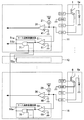
- FIG. 12 is a circuit diagram showing a conventional IPM overheat protection circuit
- FIG. 13 is a diagram showing temperature characteristics of a temperature detection diode
- (A) shows temperature vs. overheat detection voltage during chip overheat protection
- ( B) shows the temperature vs. overheat detection voltage during case overheat protection.
- the control ICs 121 to 126 are connected to the IGBTs 101 to 106, respectively, as shown in FIG. That is, the control ICs 121 to 126 each include an output terminal OUT that outputs a gate voltage, a ground terminal GND, an overcurrent detection terminal OC, and an overheat detection terminal OH.
- the output terminal OUT is connected to the gate terminals of the IGBTs 101 to 106, the ground terminal GND is connected to the emitter terminals of the IGBTs 101 to 106, and the overcurrent detection terminal OC is connected to the current sensing emitter terminals of the IGBTs 101 to 106. Yes.
- the overheat detection terminal OH is connected to the constant current source 141 and the inverting input terminal of the overheat detection comparator 142, and the non-inverting input terminal of the overheat detection comparator 142 is connected to the reference voltage source 143. Yes.
- the overheat detection terminal OH is also connected to the anode terminal of the temperature detection diode 107 of the IGBTs 101 to 106, and the cathode terminal of the temperature detection diode 107 is connected to the ground potential of the control ICs 121 to 126 via the ground terminal GND. ing.
- a constant current from the constant current source 141 is always supplied to the temperature detection diode 107, and a forward voltage corresponding to the chip temperature of the IGBTs 101 to 106 is applied to the inverting input terminal of the overheat detection comparator 142.
- the temperature characteristic of the temperature detecting diode 107 has a negative temperature characteristic as shown in FIG. 13A, and the reference voltage source 143 outputs a voltage VOH1 corresponding to a temperature of 175 ° C.
- the overheat detection comparator 142 outputs a low level protection operation signal when the chip temperature is less than 175 ° C., and outputs a high level protection operation signal when the chip temperature becomes higher than 175 ° C.
- the control ICs 121 to 126 perform control to turn off all the IGBTs 101 to 106 at the same time as outputting an alarm signal from the alarm output circuit.
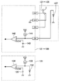
- the temperature detection IC 131 includes a temperature detection diode 132, a constant current source 133, and an overheat detection comparator 134.
- the anode terminal of the temperature detection diode 132 is connected to the constant current source 133 and the inverting input terminal of the overheat detection comparator 134, and the cathode terminal is connected to the ground.
- a non-inverting input terminal of the overheat detection comparator 134 is connected to the reference voltage source 135.
- a constant current from the constant current source 133 is always supplied to the temperature detection diode 132, and a forward voltage corresponding to the case temperature is applied to the inverting input terminal of the overheat detection comparator 134.
- the temperature characteristic of the temperature detection diode 132 has a negative temperature characteristic
- the reference voltage source 135 outputs a voltage VOH2 corresponding to a temperature of 125 ° C.
- the present invention has been made in view of these points, and an object of the present invention is to provide a semiconductor module that can detect overheating of the entire case without requiring a dedicated temperature detection IC.
- a plurality of switching elements each having a temperature detection element for detecting a chip temperature, a plurality of diodes protecting the switching elements, and a plurality of control elements for controlling the switching elements
- a semiconductor module in which a control circuit is built in one package is provided.
- the control circuit includes a comparator that compares the temperature detected by the temperature detection element with a predetermined reference temperature for the case, and at least one of the control circuits outputs at least two outputs of the comparators. And an AND circuit for judging case overheating.
- the semiconductor module having the above configuration has an advantage that the number of parts can be reduced because it can detect overheating of the case without having a dedicated temperature detection IC. Further, since the temperature of the chip that is the heat generation source is detected as the operating temperature of the case overheat protection, the detection accuracy can be improved.
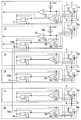
- FIG. 1 is a diagram showing a circuit configuration example of a semiconductor module according to the first embodiment
- FIG. 2 is a diagram showing temperature characteristics of a temperature detection diode.
- the semiconductor module according to the first embodiment includes a plurality of, here six, IGBTs 1 to 6, and temperature detection diodes 1 a to 6 a are formed in close contact with the respective IGBTs 1 to 6. ing.
- the control ICs 11 to 16 as control circuits each include an output terminal OUT that outputs a gate voltage, a ground terminal GND, an overcurrent detection terminal OC, and an overheat detection terminal OH.
- the output terminal OUT is connected to the gate terminals of the IGBTs 1 to 6
- the ground terminal GND is connected to the cathode terminals of the temperature detection diodes 1a to 6a
- the overcurrent detection terminal OC is a current sense of the IGBTs 1 to 6.
- the ground terminal GND is also connected to the emitter terminals of the IGBTs 2, 4, and 6.
- the control ICs 11 to 16 include constant current sources 21 to 26, chip overheat detection overheat detection comparators 31 to 36, reference voltage sources 41 to 46, case overheat detection overheat detection comparators 51 to 56, and a reference voltage. Sources 61 to 66 and AND (logical product) circuits 71 to 76 are provided.
- the overheat detection comparators 31 to 36 and the reference voltage sources 41 to 46 constitute a chip overheat protection circuit
- the overheat detection comparators 51 to 56, the reference voltage sources 61 to 66, and the AND circuits 71 to 76 are case overheat protection.
- the circuit is configured.
- the constant current sources 21 to 26 are connected to the inverting input terminals of the overheat detection comparators 31 to 36 and 51 to 56 and the overheat detection terminal OH.
- the non-inverting input terminals of the overheat detection comparators 31 to 36 and 51 to 56 are connected to the reference voltage sources 41 to 46, 61 to 66.
- the output terminals of the overheat detection comparators 31 to 36 are connected to an alarm output circuit and a gate cutoff control circuit (not shown).
- the output terminals of the overheat detection comparators 51 to 56 are connected to the overheat detection terminals 51a to 56a and one input of the AND circuits 71 to 76.
- the output terminals of the AND circuits 71 to 76 are connected to an alarm output circuit and a gate cutoff circuit (not shown).
- the AND circuits 71 to 76 have a plurality of, here six inputs.
- the overheat detection terminals 52a to 56a of the control ICs 12 to 16 are connected to the second to sixth inputs, respectively.
- the overheat detection terminals OH of the control ICs 12 to 16 are connected to the anode terminals of the temperature detection diodes 1a to 6a of the IGBTs 1 to 6, and the cathode terminals of the temperature detection diodes 1a to 6a are connected to the control ICs 11 to 11 through the ground terminal GND. It is connected to 16 ground potentials.
- Constant currents from the constant current sources 21 to 26 are always supplied to the temperature detection diodes 1a to 6a, and a forward voltage corresponding to the chip temperature of the IGBTs 1 to 6 is output to the overheat detection terminal OH as an overheat detection voltage. ing.
- the overheat detection voltage of the overheat detection terminal OH is applied to the inverting input terminals of the chip overheat detection overheat detection comparators 31 to 36 and the inverting input terminals of the case overheat detection overheat detection comparators 51 to 56.
- the temperature characteristics of the temperature detection diodes 1a to 6a have negative temperature characteristics in which the overheat detection voltage decreases as the temperature increases.
- the reference voltage sources 41 to 46 of the chip overheat protection circuit output a voltage VOH1 corresponding to a temperature of 175 ° C.
- the reference voltage sources 61 to 66 of the case overheat protection circuit have a temperature of 125 ° C. (predetermined reference temperature). ) Is output.
- the overheat detection threshold voltages output from the reference voltage sources 41 to 46 and 61 to 66 can be selected from voltages corresponding to values other than 175 ° C. and 125 ° C.
- the overheat detection comparators 31 to 36 output a low level protection operation signal, and any one of the IGBTs 1 to 6 has a high temperature of 175 ° C. or higher. Then, a high level protection operation signal is output.
- the control ICs 11 to 16 to which the high-level protection operation signal is output perform control to turn off all the IGBTs 1 to 6 at the same time as outputting the alarm signal from the alarm output circuit.
- the overheat detection comparators 51 to 56 when the chip temperature of the IGBTs 1 to 6 is less than 125 ° C., the overheat detection comparators 51 to 56 output a low level protection operation signal, and when the chip temperature becomes higher than the medium temperature of 125 ° C., the high level protection operation signal Is output.
- the protection operation signals of the overheat detection comparators 51 to 56 are input to the AND circuit 71 in the case overheat protection circuit of the control IC 11. Therefore, the AND circuit 71 determines that the case is in an overheated state when all of the overheat detection comparators 51 to 56 detect a chip temperature equal to or higher than the intermediate temperature, and outputs a high-level protection operation signal to the overheat detection terminal 51b. To do.
- the protection operation signal of the overheat detection terminal 51b performs control to turn off all the IGBTs 1 to 6 at the same time as outputting an alarm signal from the alarm output circuit.
- the case overheating state is determined by performing an AND operation on the detection results of all the temperature detection diodes 1a to 6a.
- the temperature detection IC for case overheating protection that is provided independently in the conventional semiconductor module, leading to a reduction in the number of parts. Further, since the chip temperature, which is the heat source of the IPM, is directly detected with respect to the operating temperature of the case overheat protection, the detection accuracy can be improved.
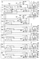
- FIG. 3 is a diagram showing a circuit configuration example of the semiconductor module according to the second embodiment.
- symbol is attached
- some components of the V-phase and W-phase control ICs 13 to 16 are omitted.
- the semiconductor module according to the second embodiment includes the temperature detecting diodes 1a of the three IGBTs 1, 3, and 5 in each upper arm portion among the IGBTs 1 to 6 constituting the U-phase, V-phase, and W-phase arm portions. , 3a, 5a is used to determine the overheating state of the case. Therefore, the AND circuits 71 to 76 of the control ICs 11 to 16 are constituted by a three-input AND circuit.
- the AND circuit 71 of the control IC 11 receives the outputs of the overheat detection comparators 51, 53, 55, and the temperature detection diodes 1a, 3a, 5a of the three IGBTs 1, 3, 5 all detect overheat temperatures of 125 ° C. or more. Output a high level protection operation signal.
- the control ICs 11 to 16 determine that the case is in an overheated state and output an alarm signal from the alarm output circuit, and at the same time, all the IGBTs 1 to 6 are turned off. Take control.
- the logical product operation of the overheat detection voltage is performed by the AND circuit 71 of the control IC 11.
- any one of the AND circuits 71 to 76 of the control ICs 11 to 16 may be used.
- FIG. 4 is a diagram illustrating a circuit configuration example of the semiconductor module according to the third embodiment.
- symbol is attached
- some components of the V-phase and W-phase control ICs 13 to 16 are omitted.
- the semiconductor module according to the third embodiment includes a temperature detecting diode 2a for three IGBTs 2, 4 and 6 in each lower arm among the IGBTs 1 to 6 constituting the U-phase, V-phase and W-phase arm portions. , 4a, 6a is used to determine whether the case is overheated. Therefore, the AND circuits 71 to 76 of the control ICs 11 to 16 are constituted by a three-input AND circuit.
- the AND circuit 72 of the control IC 12 receives the outputs of the overheat detection comparators 52, 54, and 56, and the temperature detection diodes 2a, 4a, and 6a of the three IGBTs 2, 4, and 6 all detect overheat temperatures of 125 ° C. or higher. Output a high level protection operation signal.
- the control ICs 11 to 16 determine that the case is in an overheated state and output an alarm signal from the alarm output circuit, and at the same time, all the IGBTs 1 to 6 are turned off. Take control.
- the AND operation of the overheat detection voltage is performed by the AND circuit 72 of the control IC 12.
- any one of the AND circuits 71 to 76 of the control ICs 11 to 16 may be used.
- the AND circuit 71 of the control IC 11 may be used.
- FIG. 5 is a diagram showing a circuit configuration example of the semiconductor module according to the fourth embodiment.
- symbol is attached
- some components of the V-phase and W-phase control ICs 13 to 16 are omitted.
- the chip temperatures at three locations in total that is, two in the upper arm portion and one in the lower arm portion. Based on this, the case overheat condition is judged.
- the overheat state of the case is determined based on the overheat detection voltage by the temperature detection diodes 1a and 5a of the two IGBTs 1 and 5 in the upper arm part and the temperature detection diode 4a of the one IGBT 4 in the lower arm part. Deciding.
- the AND circuits 71 to 76 of the control ICs 11 to 16 are configured by a three-input AND circuit.
- the AND circuit 71 of the control IC 11 receives the outputs of the overheat detection comparators 51, 54, 55, and the temperature detection diodes 1a, 4a, 5a of the three IGBTs 1, 4, 5 all detect overheat temperatures of 125 ° C. or more. Output a high level protection operation signal.
- the control ICs 11 to 16 determine that the case is in an overheated state and output an alarm signal from the alarm output circuit, and at the same time, all the IGBTs 1 to 6 are turned off. Take control.
- the AND operation of the overheat detection voltage is performed by the AND circuit 71 of the control IC 11.
- any one of the AND circuits 71 to 76 of the control ICs 11 to 16 may be used.
- the AND circuit 72 of the control IC 12 may be used.
- the chip temperatures of the two IGBTs 1 and 5 in the upper arm portion are observed, but the chip temperatures of the IGBTs 1 and 3 or the IGBTs 3 and 5 may be observed.
- the chip temperature of one IGBT 4 in the lower arm part is observed, but the chip temperature of IGBT 2 or IGBT 6 may be observed.
- FIG. 6 is a diagram illustrating a circuit configuration example of the semiconductor module according to the fifth embodiment.
- symbol is attached
- some components of the V-phase and W-phase control ICs 13 to 16 are omitted.
- the semiconductor module according to the fifth embodiment includes a total of three chip temperatures, one of the upper arm part and the lower arm part, of the IGBTs 1 to 6 constituting the U-phase, V-phase, and W-phase arm parts. Based on this, the case overheat condition is judged. In this embodiment, the overheat state of the case is determined based on the overheat detection voltage by the temperature detection diode 3a of one IGBT 3 in the upper arm part and the temperature detection diodes 2a and 6a of the two IGBTs 2 and 6 in the lower arm part. Deciding. In order to collect the three overheat detection voltages, the AND circuits 71 to 76 of the control ICs 11 to 16 are configured by a three-input AND circuit.
- the AND circuit 72 of the control IC 12 receives the output of the overheat detection comparators 52, 53, and 56, and the temperature detection diodes 2a, 3a, and 6a of the three IGBTs 2, 3, and 6 all detect overheat temperatures of 125 ° C. or more. Output a high level protection operation signal.
- the control ICs 11 to 16 determine that the case is in an overheated state and output an alarm signal from the alarm output circuit, and at the same time, all the IGBTs 1 to 6 are turned off. Take control.
- the AND operation of the overheat detection voltage is performed by the AND circuit 72 of the control IC 12.
- any one of the AND circuits 71 to 76 of the control ICs 11 to 16 may be used.
- the AND circuit 71 of the control IC 11 may be used.
- the chip temperature of one IGBT 3 in the upper arm portion is observed, but the chip temperature of IGBT 1 or IGBT 5 may be observed.
- the chip temperatures of the two IGBTs 2 and 6 in the lower arm portion are observed, but the chip temperatures of the IGBTs 2 and 4 or the IGBTs 4 and 6 may be observed.
- FIG. 7 is a diagram showing a circuit configuration example of the semiconductor module according to the sixth embodiment.
- symbol is attached
- some components of the V-phase and W-phase control ICs 13 to 16 are omitted.
- the semiconductor module according to the sixth embodiment includes a total of four chip temperatures, one of the upper arm part and three of the lower arm parts among the IGBTs 1 to 6 constituting the U-phase, V-phase, and W-phase arm parts. Based on this, the case overheat condition is judged. In this embodiment, the case is based on the overheat detection voltage by the temperature detection diode 3a of one IGBT 3 in the upper arm part and the temperature detection diodes 2a, 4a, 6a of the three IGBTs 2, 4, 6 in the lower arm part. Judgment of overheating condition. In order to collect the four overheat detection voltages, the AND circuits 71 to 76 of the control ICs 11 to 16 are constituted by 4-input AND circuits.
- the AND circuit 72 of the control IC 12 inputs the output of the overheat detection comparators 52, 53, 54, and 56, and the temperature detection diodes 2a, 3a, 4a, and 6a of the four IGBTs 2, 3, 4, and 6 are all 125 ° C. or higher.
- a high level protection operation signal is output.
- the control ICs 11 to 16 determine that the case is in an overheated state and output an alarm signal from the alarm output circuit, and at the same time, all the IGBTs 1 to 6 are turned off. Take control.
- the AND operation of the overheat detection voltage is performed by the AND circuit 72 of the control IC 12.
- any one of the AND circuits 71 to 76 of the control ICs 11 to 16 may be used.
- the AND circuit 71 of the control IC 11 may be used.
- the chip temperature of one IGBT 3 in the upper arm portion is observed, but the chip temperature of IGBT 1 or IGBT 5 may be observed.
- FIG. 8 is a diagram showing a circuit configuration example of the semiconductor module according to the seventh embodiment.
- symbol is attached
- some components of the V-phase and W-phase control ICs 13 to 16 are omitted.
- the semiconductor module according to the seventh embodiment includes a total of four chip temperatures, three of the upper arm part and one of the lower arm part among the IGBTs 1 to 6 constituting the U-phase, V-phase, and W-phase arm parts. Based on this, the case overheat condition is judged. In this embodiment, the case is based on the overheat detection voltage by the temperature detection diodes 1a, 3a, 5a of the three IGBTs 1, 3, 5 in the upper arm part and the temperature detection diode 4a of the IGBT 4 in the lower arm part. Judgment of overheating condition. In order to collect the four overheat detection voltages, the AND circuits 71 to 76 of the control ICs 11 to 16 are constituted by 4-input AND circuits.
- the AND circuit 71 of the control IC 11 receives the outputs of the overheat detection comparators 51, 53, 54, 55, and the temperature detection diodes 1a, 3a, 4a, 5a of the four IGBTs 1, 3, 4, 5 are all 125 ° C. or higher.
- a high level protection operation signal is output.
- the control ICs 11 to 16 determine that the case is in an overheated state and output an alarm signal from the alarm output circuit, and at the same time, all the IGBTs 1 to 6 are turned off. Take control.
- the AND operation of the overheat detection voltage is performed by the AND circuit 71 of the control IC 11.
- any one of the AND circuits 71 to 76 of the control ICs 11 to 16 may be used.
- the AND circuit 72 of the control IC 12 may be used.
- the chip temperature of one IGBT 4 in the lower arm portion is observed, but the chip temperature of IGBT 2 or IGBT 6 may be observed.
- FIG. 9 is a diagram showing a circuit configuration example of the semiconductor module according to the eighth embodiment.
- symbol is attached
- some components of the V-phase and W-phase control ICs 13 to 16 are omitted.
- the semiconductor module according to the eighth embodiment includes a total of four chip temperatures, two of the upper arm portion and two of the lower arm portion among the IGBTs 1 to 6 constituting the U-phase, V-phase, and W-phase arm portions. Based on this, the case overheat condition is judged. In this embodiment, the case is based on the overheat detection voltage by the temperature detection diodes 1a and 5a of the two IGBTs 1 and 5 in the upper arm part and the temperature detection diodes 2a and 6a of the two IGBTs 2 and 6 in the lower arm part. Judgment of overheating condition. In order to collect the four overheat detection voltages, the AND circuits 71 to 76 of the control ICs 11 to 16 are constituted by 4-input AND circuits.
- the AND circuit 71 of the control IC 11 inputs the outputs of the overheat detection comparators 51, 52, 55, 56, and the temperature detection diodes 1a, 2a, 5a, 6a of the four IGBTs 1, 2, 5, 6 are all 125 ° C. or higher.
- a high level protection operation signal is output.
- the control ICs 11 to 16 determine that the case is in an overheated state and output an alarm signal from the alarm output circuit, and at the same time, all the IGBTs 1 to 6 are turned off. Take control.
- the AND operation of the overheat detection voltage is performed by the AND circuit 71 of the control IC 11.
- any one of the AND circuits 71 to 76 of the control ICs 11 to 16 may be used.
- the AND circuit 72 of the control IC 12 may be used.
- the chip temperatures of the two IGBTs 1 and 5 in the upper arm portion are observed, but the chip temperatures of the IGBTs 1 and 3 or the IGBTs 3 and 5 may be observed.
- the chip temperatures of the two IGBTs 2 and 6 in the lower arm portion are observed, but the chip temperatures of the IGBTs 2 and 4 or the IGBTs 4 and 6 may be observed.
- FIG. 10 is a diagram showing a circuit configuration example of the semiconductor module according to the ninth embodiment.
- symbol is attached
- some components of the V-phase and W-phase control ICs 13 to 16 are omitted.
- case overheating is detected by observing the chip temperature of all IGBTs 1 to 6, and overheating detection is performed on the diodes 91 to 96 connected in reverse parallel to the respective IGBTs 1 to 6. It is.
- diodes 91 and 92, diodes 93 and 94 and diodes 95 and 96 are sandwiched between IGBTs 1, 2, IGBTs 3 and 4, and IGBTs 5 and 6 in each arm part. This is possible in the case of such a layout.
- the case overheat protection circuit is additionally provided with a diode overheat detection function.
- the control ICs 11 to 16 has a case overheat protection circuit having a diode overheat detection function, and the other five (control ICs 12 to 16) have a diode overheat detection function.
- the case where it is set as the structure which does not have is illustrated.
- the case overheat protection circuit of the control IC 11 includes an overheat detection comparator 51 for detecting case overheat, a reference voltage source 61, an AND circuit 71 with two inputs, and a 3-input AND circuit 71a, and a three-input OR circuit for detecting diode overheat. (OR circuit) 81 is provided.
- the case overheat protection circuit of the control ICs 12 to 16 includes overheat detection comparators 52 to 56, reference voltage sources 62 to 66, and 2-input AND circuits 72 to 76.
- the outputs of the overheat detection comparators 51 and 52 are input to the AND circuit 71
- the outputs of the overheat detection comparators 53 and 54 are input to the AND circuit 73
- the overheat is detected.
- the outputs of the detection comparators 55 and 56 are input to the AND circuit 75.
- the outputs of the AND circuits 71, 73, and 75 are input to the AND circuit 71a, and the output of the AND circuit 71a is connected to the overheat detection terminal 51c.
- the control IC 11 outputs an alarm signal from the alarm output circuit and simultaneously turns off all the IGBTs 1 to 6. To be controlled.
- the outputs of the AND circuits 71, 73 and 75 are also input to the OR circuit 81, and the output of the OR circuit 81 is connected to the overheat detection terminal 51d.
- the alarm output circuit that has received the high-level protection operation signal from the overheat detection terminal 51d outputs the alarm signal.
- the semiconductor module of the ninth embodiment in addition to the case overheat detection function, it is also possible to detect overheat of the diodes 91 to 96 that generate heat but do not have a temperature detection function like the IGBTs 1 to 6. ing.
- the IPM provided with six switching elements has been described as an example.
- the present invention is not limited to such an IPM, and can be applied to a semiconductor module including any number of two or more switching elements.
Landscapes
- Engineering & Computer Science (AREA)
- Power Engineering (AREA)
- Inverter Devices (AREA)
- Electronic Switches (AREA)
- Power Conversion In General (AREA)
Abstract
Priority Applications (4)
| Application Number | Priority Date | Filing Date | Title |
|---|---|---|---|
| CN201580011304.0A CN106063109B (zh) | 2014-09-09 | 2015-09-08 | 半导体模块 |
| JP2016547453A JP6260710B2 (ja) | 2014-09-09 | 2015-09-08 | 半導体モジュール |
| DE112015000606.0T DE112015000606T5 (de) | 2014-09-09 | 2015-09-08 | Halbleitermodul |
| US15/255,127 US10020297B2 (en) | 2014-09-09 | 2016-09-01 | Semiconductor module |
Applications Claiming Priority (2)
| Application Number | Priority Date | Filing Date | Title |
|---|---|---|---|
| JP2014183090 | 2014-09-09 | ||
| JP2014-183090 | 2014-09-09 |
Related Child Applications (1)
| Application Number | Title | Priority Date | Filing Date |
|---|---|---|---|
| US15/255,127 Continuation US10020297B2 (en) | 2014-09-09 | 2016-09-01 | Semiconductor module |
Publications (1)
| Publication Number | Publication Date |
|---|---|
| WO2016039342A1 true WO2016039342A1 (fr) | 2016-03-17 |
Family
ID=55459086
Family Applications (1)
| Application Number | Title | Priority Date | Filing Date |
|---|---|---|---|
| PCT/JP2015/075477 Ceased WO2016039342A1 (fr) | 2014-09-09 | 2015-09-08 | Module semiconducteur |
Country Status (5)
| Country | Link |
|---|---|
| US (1) | US10020297B2 (fr) |
| JP (1) | JP6260710B2 (fr) |
| CN (1) | CN106063109B (fr) |
| DE (1) | DE112015000606T5 (fr) |
| WO (1) | WO2016039342A1 (fr) |
Cited By (2)
| Publication number | Priority date | Publication date | Assignee | Title |
|---|---|---|---|---|
| JP2021150820A (ja) * | 2020-03-19 | 2021-09-27 | 富士電機株式会社 | 半導体装置およびその過電流保護機能 |
| JP2022037262A (ja) * | 2020-08-25 | 2022-03-09 | 富士電機株式会社 | 半導体装置 |
Families Citing this family (5)
| Publication number | Priority date | Publication date | Assignee | Title |
|---|---|---|---|---|
| CN110611298B (zh) * | 2019-09-10 | 2025-01-07 | 沈阳微控飞轮技术股份有限公司 | 用于飞轮储能装置的ipm保护系统 |
| JP7472663B2 (ja) * | 2020-06-05 | 2024-04-23 | 富士電機株式会社 | 電力変換装置 |
| JP7388318B2 (ja) * | 2020-09-02 | 2023-11-29 | トヨタ自動車株式会社 | 電源装置 |
| JP7639583B2 (ja) * | 2021-06-29 | 2025-03-05 | 富士電機株式会社 | 半導体モジュール、及び半導体モジュールの製造方法 |
| CN117134757B (zh) * | 2023-10-25 | 2024-01-19 | 晶艺半导体有限公司 | 半导体合封器件及其过温保护电路和方法 |
Citations (3)
| Publication number | Priority date | Publication date | Assignee | Title |
|---|---|---|---|---|
| JP2008263774A (ja) * | 2007-04-12 | 2008-10-30 | Schneider Toshiba Inverter Europe Sas | 可変速駆動装置の温度管理方法およびシステム |
| WO2013046309A1 (fr) * | 2011-09-27 | 2013-04-04 | トヨタ自動車株式会社 | Dispositif de détection de problème de dispositif de refroidissement et procédé de détection de problème |
| WO2014129052A1 (fr) * | 2013-02-21 | 2014-08-28 | ダイキン工業株式会社 | Dispositif d'estimation de température et dispositif semiconducteur |
Family Cites Families (13)
| Publication number | Priority date | Publication date | Assignee | Title |
|---|---|---|---|---|
| US5325258A (en) * | 1992-08-26 | 1994-06-28 | International Rectifier Corporation | Power transistor driver circuit with current sensing and current overprotection and method for protecting power transistor from overcurrent |
| JP2999887B2 (ja) * | 1992-10-09 | 2000-01-17 | 三菱電機株式会社 | Igbtの過電流保護回路及び半導体集積回路装置 |
| US5563759A (en) * | 1995-04-11 | 1996-10-08 | International Rectifier Corporation | Protected three-pin mosgated power switch with separate input reset signal level |
| JP4040838B2 (ja) | 2000-12-18 | 2008-01-30 | 三菱電機株式会社 | 電力用半導体装置 |
| JP2003125588A (ja) * | 2001-10-12 | 2003-04-25 | Mitsubishi Electric Corp | 電力変換装置 |
| JP5161641B2 (ja) * | 2008-04-18 | 2013-03-13 | 株式会社東芝 | 温度検出回路 |
| JP4829999B2 (ja) * | 2009-05-08 | 2011-12-07 | パナソニック株式会社 | 電源装置及び電池パック |
| JP4844653B2 (ja) * | 2009-07-20 | 2011-12-28 | 株式会社デンソー | パワースイッチング素子の駆動装置 |
| JP5360002B2 (ja) | 2010-06-28 | 2013-12-04 | 富士電機株式会社 | 半導体素子の駆動装置 |
| US8657489B2 (en) | 2010-06-28 | 2014-02-25 | Infineon Technologies Ag | Power switch temperature control device and method |
| JP5263321B2 (ja) * | 2011-02-25 | 2013-08-14 | 株式会社デンソー | 温度検出装置 |
| EP2696493B1 (fr) * | 2011-04-08 | 2017-09-06 | Fuji Electric Co., Ltd. | Contrôleur de convertisseur de puissance |
| JP5295405B1 (ja) | 2012-04-04 | 2013-09-18 | 三菱電機株式会社 | スイッチ素子の温度検出回路 |
-
2015
- 2015-09-08 CN CN201580011304.0A patent/CN106063109B/zh active Active
- 2015-09-08 WO PCT/JP2015/075477 patent/WO2016039342A1/fr not_active Ceased
- 2015-09-08 DE DE112015000606.0T patent/DE112015000606T5/de active Pending
- 2015-09-08 JP JP2016547453A patent/JP6260710B2/ja active Active
-
2016
- 2016-09-01 US US15/255,127 patent/US10020297B2/en active Active
Patent Citations (3)
| Publication number | Priority date | Publication date | Assignee | Title |
|---|---|---|---|---|
| JP2008263774A (ja) * | 2007-04-12 | 2008-10-30 | Schneider Toshiba Inverter Europe Sas | 可変速駆動装置の温度管理方法およびシステム |
| WO2013046309A1 (fr) * | 2011-09-27 | 2013-04-04 | トヨタ自動車株式会社 | Dispositif de détection de problème de dispositif de refroidissement et procédé de détection de problème |
| WO2014129052A1 (fr) * | 2013-02-21 | 2014-08-28 | ダイキン工業株式会社 | Dispositif d'estimation de température et dispositif semiconducteur |
Cited By (5)
| Publication number | Priority date | Publication date | Assignee | Title |
|---|---|---|---|---|
| JP2021150820A (ja) * | 2020-03-19 | 2021-09-27 | 富士電機株式会社 | 半導体装置およびその過電流保護機能 |
| US11594873B2 (en) | 2020-03-19 | 2023-02-28 | Fuji Electric Co., Ltd. | Semiconductor device and overcurrent protection method |
| JP7612997B2 (ja) | 2020-03-19 | 2025-01-15 | 富士電機株式会社 | 半導体装置およびその過電流保護機能 |
| JP2022037262A (ja) * | 2020-08-25 | 2022-03-09 | 富士電機株式会社 | 半導体装置 |
| JP7600565B2 (ja) | 2020-08-25 | 2024-12-17 | 富士電機株式会社 | 半導体装置 |
Also Published As
| Publication number | Publication date |
|---|---|
| DE112015000606T5 (de) | 2016-11-03 |
| CN106063109A (zh) | 2016-10-26 |
| US20160372454A1 (en) | 2016-12-22 |
| JPWO2016039342A1 (ja) | 2017-04-27 |
| CN106063109B (zh) | 2018-11-09 |
| US10020297B2 (en) | 2018-07-10 |
| JP6260710B2 (ja) | 2018-01-17 |
Similar Documents
| Publication | Publication Date | Title |
|---|---|---|
| JP6260710B2 (ja) | 半導体モジュール | |
| JP5360002B2 (ja) | 半導体素子の駆動装置 | |
| JP4892032B2 (ja) | 電力変換装置 | |
| US10778001B2 (en) | Overcurrent detection circuit and power converter | |
| CN107924872B (zh) | 绝缘栅半导体装置 | |
| CN112787489B (zh) | 半导体装置的驱动装置及驱动方法和电力变换装置 | |
| JP5974548B2 (ja) | 半導体装置 | |
| JP2015032984A (ja) | 半導体素子の駆動装置およびそれを用いた電力変換装置 | |
| US20160241242A1 (en) | Drive unit | |
| CN106849018A (zh) | 半导体元件的驱动装置 | |
| JP6107949B2 (ja) | 半導体モジュール | |
| CN102810852B (zh) | 半导体装置 | |
| US20170126145A1 (en) | Methods and Systems for Interconnecting Parallel IGBT Modules | |
| US12597852B2 (en) | Protecting a power inverter by sensing a phase node voltage | |
| US20140118873A1 (en) | Power module and apparatus for preventing malfunction, and method of controlling thereof | |
| US9667129B2 (en) | Power conversion device with overcurrent protection | |
| JP2009165285A (ja) | 半導体装置 | |
| JP5182243B2 (ja) | パワーモジュール | |
| JP6950828B2 (ja) | 駆動回路内蔵型パワーモジュール | |
| JP2019176696A (ja) | パワートランジスタの駆動回路、パワーモジュール | |
| CN110880859B (zh) | 半导体模块及电力转换装置 | |
| JP2024042801A (ja) | 半導体モジュール | |
| CN114944774A (zh) | 电力转换装置 | |
| JP7513201B2 (ja) | 過電流検出回路、駆動制御装置および電力変換装置 | |
| JP2007059738A (ja) | 保護回路を備えた半導体装置 |
Legal Events
| Date | Code | Title | Description |
|---|---|---|---|
| 121 | Ep: the epo has been informed by wipo that ep was designated in this application |
Ref document number: 15840272 Country of ref document: EP Kind code of ref document: A1 |
|
| WWE | Wipo information: entry into national phase |
Ref document number: 112015000606 Country of ref document: DE |
|
| ENP | Entry into the national phase |
Ref document number: 2016547453 Country of ref document: JP Kind code of ref document: A |
|
| 122 | Ep: pct application non-entry in european phase |
Ref document number: 15840272 Country of ref document: EP Kind code of ref document: A1 |