WO2016068585A1 - 유기 전계 발광 소자 - Google Patents
유기 전계 발광 소자 Download PDFInfo
- Publication number
- WO2016068585A1 WO2016068585A1 PCT/KR2015/011393 KR2015011393W WO2016068585A1 WO 2016068585 A1 WO2016068585 A1 WO 2016068585A1 KR 2015011393 W KR2015011393 W KR 2015011393W WO 2016068585 A1 WO2016068585 A1 WO 2016068585A1
- Authority
- WO
- WIPO (PCT)
- Prior art keywords
- electron transport
- group
- transport material
- organic
- substituted
- Prior art date
- Legal status (The legal status is an assumption and is not a legal conclusion. Google has not performed a legal analysis and makes no representation as to the accuracy of the status listed.)
- Ceased
Links
Images

Classifications
-
- H—ELECTRICITY
- H10—SEMICONDUCTOR DEVICES; ELECTRIC SOLID-STATE DEVICES NOT OTHERWISE PROVIDED FOR
- H10K—ORGANIC ELECTRIC SOLID-STATE DEVICES
- H10K85/00—Organic materials used in the body or electrodes of devices covered by this subclass
- H10K85/60—Organic compounds having low molecular weight
- H10K85/649—Aromatic compounds comprising a hetero atom
- H10K85/654—Aromatic compounds comprising a hetero atom comprising only nitrogen as heteroatom
-
- C—CHEMISTRY; METALLURGY
- C07—ORGANIC CHEMISTRY
- C07D—HETEROCYCLIC COMPOUNDS
- C07D209/00—Heterocyclic compounds containing five-membered rings, condensed with other rings, with one nitrogen atom as the only ring hetero atom
- C07D209/56—Ring systems containing three or more rings
- C07D209/80—[b, c]- or [b, d]-condensed
- C07D209/82—Carbazoles; Hydrogenated carbazoles
- C07D209/86—Carbazoles; Hydrogenated carbazoles with only hydrogen atoms, hydrocarbon or substituted hydrocarbon radicals, directly attached to carbon atoms of the ring system
-
- C—CHEMISTRY; METALLURGY
- C07—ORGANIC CHEMISTRY
- C07C—ACYCLIC OR CARBOCYCLIC COMPOUNDS
- C07C255/00—Carboxylic acid nitriles
- C07C255/49—Carboxylic acid nitriles having cyano groups bound to carbon atoms of six-membered aromatic rings of a carbon skeleton
- C07C255/50—Carboxylic acid nitriles having cyano groups bound to carbon atoms of six-membered aromatic rings of a carbon skeleton to carbon atoms of non-condensed six-membered aromatic rings
-
- C—CHEMISTRY; METALLURGY
- C07—ORGANIC CHEMISTRY
- C07D—HETEROCYCLIC COMPOUNDS
- C07D209/00—Heterocyclic compounds containing five-membered rings, condensed with other rings, with one nitrogen atom as the only ring hetero atom
- C07D209/56—Ring systems containing three or more rings
- C07D209/80—[b, c]- or [b, d]-condensed
- C07D209/82—Carbazoles; Hydrogenated carbazoles
-
- C—CHEMISTRY; METALLURGY
- C07—ORGANIC CHEMISTRY
- C07D—HETEROCYCLIC COMPOUNDS
- C07D235/00—Heterocyclic compounds containing 1,3-diazole or hydrogenated 1,3-diazole rings, condensed with other rings
- C07D235/02—Heterocyclic compounds containing 1,3-diazole or hydrogenated 1,3-diazole rings, condensed with other rings condensed with carbocyclic rings or ring systems
- C07D235/04—Benzimidazoles; Hydrogenated benzimidazoles
- C07D235/06—Benzimidazoles; Hydrogenated benzimidazoles with only hydrogen atoms, hydrocarbon or substituted hydrocarbon radicals, directly attached in position 2
- C07D235/08—Radicals containing only hydrogen and carbon atoms
-
- C—CHEMISTRY; METALLURGY
- C07—ORGANIC CHEMISTRY
- C07D—HETEROCYCLIC COMPOUNDS
- C07D239/00—Heterocyclic compounds containing 1,3-diazine or hydrogenated 1,3-diazine rings
- C07D239/02—Heterocyclic compounds containing 1,3-diazine or hydrogenated 1,3-diazine rings not condensed with other rings
- C07D239/24—Heterocyclic compounds containing 1,3-diazine or hydrogenated 1,3-diazine rings not condensed with other rings having three or more double bonds between ring members or between ring members and non-ring members
- C07D239/26—Heterocyclic compounds containing 1,3-diazine or hydrogenated 1,3-diazine rings not condensed with other rings having three or more double bonds between ring members or between ring members and non-ring members with only hydrogen atoms, hydrocarbon or substituted hydrocarbon radicals, directly attached to ring carbon atoms
-
- C—CHEMISTRY; METALLURGY
- C07—ORGANIC CHEMISTRY
- C07D—HETEROCYCLIC COMPOUNDS
- C07D251/00—Heterocyclic compounds containing 1,3,5-triazine rings
- C07D251/02—Heterocyclic compounds containing 1,3,5-triazine rings not condensed with other rings
- C07D251/12—Heterocyclic compounds containing 1,3,5-triazine rings not condensed with other rings having three double bonds between ring members or between ring members and non-ring members
- C07D251/14—Heterocyclic compounds containing 1,3,5-triazine rings not condensed with other rings having three double bonds between ring members or between ring members and non-ring members with hydrogen or carbon atoms directly attached to at least one ring carbon atom
- C07D251/24—Heterocyclic compounds containing 1,3,5-triazine rings not condensed with other rings having three double bonds between ring members or between ring members and non-ring members with hydrogen or carbon atoms directly attached to at least one ring carbon atom to three ring carbon atoms
-
- C—CHEMISTRY; METALLURGY
- C07—ORGANIC CHEMISTRY
- C07D—HETEROCYCLIC COMPOUNDS
- C07D263/00—Heterocyclic compounds containing 1,3-oxazole or hydrogenated 1,3-oxazole rings
- C07D263/52—Heterocyclic compounds containing 1,3-oxazole or hydrogenated 1,3-oxazole rings condensed with carbocyclic rings or ring systems
- C07D263/54—Benzoxazoles; Hydrogenated benzoxazoles
- C07D263/56—Benzoxazoles; Hydrogenated benzoxazoles with only hydrogen atoms, hydrocarbon or substituted hydrocarbon radicals, directly attached in position 2
- C07D263/57—Aryl or substituted aryl radicals
-
- C—CHEMISTRY; METALLURGY
- C07—ORGANIC CHEMISTRY
- C07D—HETEROCYCLIC COMPOUNDS
- C07D277/00—Heterocyclic compounds containing 1,3-thiazole or hydrogenated 1,3-thiazole rings
- C07D277/60—Heterocyclic compounds containing 1,3-thiazole or hydrogenated 1,3-thiazole rings condensed with carbocyclic rings or ring systems
- C07D277/62—Benzothiazoles
- C07D277/64—Benzothiazoles with only hydrocarbon or substituted hydrocarbon radicals attached in position 2
- C07D277/66—Benzothiazoles with only hydrocarbon or substituted hydrocarbon radicals attached in position 2 with aromatic rings or ring systems directly attached in position 2
-
- C—CHEMISTRY; METALLURGY
- C07—ORGANIC CHEMISTRY
- C07D—HETEROCYCLIC COMPOUNDS
- C07D401/00—Heterocyclic compounds containing two or more hetero rings, having nitrogen atoms as the only ring hetero atoms, at least one ring being a six-membered ring with only one nitrogen atom
- C07D401/02—Heterocyclic compounds containing two or more hetero rings, having nitrogen atoms as the only ring hetero atoms, at least one ring being a six-membered ring with only one nitrogen atom containing two hetero rings
- C07D401/10—Heterocyclic compounds containing two or more hetero rings, having nitrogen atoms as the only ring hetero atoms, at least one ring being a six-membered ring with only one nitrogen atom containing two hetero rings linked by a carbon chain containing aromatic rings
-
- C—CHEMISTRY; METALLURGY
- C07—ORGANIC CHEMISTRY
- C07D—HETEROCYCLIC COMPOUNDS
- C07D401/00—Heterocyclic compounds containing two or more hetero rings, having nitrogen atoms as the only ring hetero atoms, at least one ring being a six-membered ring with only one nitrogen atom
- C07D401/14—Heterocyclic compounds containing two or more hetero rings, having nitrogen atoms as the only ring hetero atoms, at least one ring being a six-membered ring with only one nitrogen atom containing three or more hetero rings
-
- C—CHEMISTRY; METALLURGY
- C07—ORGANIC CHEMISTRY
- C07D—HETEROCYCLIC COMPOUNDS
- C07D403/00—Heterocyclic compounds containing two or more hetero rings, having nitrogen atoms as the only ring hetero atoms, not provided for by group C07D401/00
- C07D403/02—Heterocyclic compounds containing two or more hetero rings, having nitrogen atoms as the only ring hetero atoms, not provided for by group C07D401/00 containing two hetero rings
- C07D403/10—Heterocyclic compounds containing two or more hetero rings, having nitrogen atoms as the only ring hetero atoms, not provided for by group C07D401/00 containing two hetero rings linked by a carbon chain containing aromatic rings
-
- C—CHEMISTRY; METALLURGY
- C07—ORGANIC CHEMISTRY
- C07D—HETEROCYCLIC COMPOUNDS
- C07D403/00—Heterocyclic compounds containing two or more hetero rings, having nitrogen atoms as the only ring hetero atoms, not provided for by group C07D401/00
- C07D403/14—Heterocyclic compounds containing two or more hetero rings, having nitrogen atoms as the only ring hetero atoms, not provided for by group C07D401/00 containing three or more hetero rings
-
- C—CHEMISTRY; METALLURGY
- C09—DYES; PAINTS; POLISHES; NATURAL RESINS; ADHESIVES; COMPOSITIONS NOT OTHERWISE PROVIDED FOR; APPLICATIONS OF MATERIALS NOT OTHERWISE PROVIDED FOR
- C09K—MATERIALS FOR MISCELLANEOUS APPLICATIONS, NOT PROVIDED FOR ELSEWHERE
- C09K11/00—Luminescent materials, e.g. electroluminescent or chemiluminescent
- C09K11/02—Use of particular materials as binders, particle coatings or suspension media therefor
- C09K11/025—Use of particular materials as binders, particle coatings or suspension media therefor non-luminescent particle coatings or suspension media
-
- C—CHEMISTRY; METALLURGY
- C09—DYES; PAINTS; POLISHES; NATURAL RESINS; ADHESIVES; COMPOSITIONS NOT OTHERWISE PROVIDED FOR; APPLICATIONS OF MATERIALS NOT OTHERWISE PROVIDED FOR
- C09K—MATERIALS FOR MISCELLANEOUS APPLICATIONS, NOT PROVIDED FOR ELSEWHERE
- C09K11/00—Luminescent materials, e.g. electroluminescent or chemiluminescent
- C09K11/06—Luminescent materials, e.g. electroluminescent or chemiluminescent containing organic luminescent materials
-
- H—ELECTRICITY
- H10—SEMICONDUCTOR DEVICES; ELECTRIC SOLID-STATE DEVICES NOT OTHERWISE PROVIDED FOR
- H10K—ORGANIC ELECTRIC SOLID-STATE DEVICES
- H10K50/00—Organic light-emitting devices
-
- H—ELECTRICITY
- H10—SEMICONDUCTOR DEVICES; ELECTRIC SOLID-STATE DEVICES NOT OTHERWISE PROVIDED FOR
- H10K—ORGANIC ELECTRIC SOLID-STATE DEVICES
- H10K50/00—Organic light-emitting devices
- H10K50/10—OLEDs or polymer light-emitting diodes [PLED]
-
- H—ELECTRICITY
- H10—SEMICONDUCTOR DEVICES; ELECTRIC SOLID-STATE DEVICES NOT OTHERWISE PROVIDED FOR
- H10K—ORGANIC ELECTRIC SOLID-STATE DEVICES
- H10K50/00—Organic light-emitting devices
- H10K50/10—OLEDs or polymer light-emitting diodes [PLED]
- H10K50/14—Carrier transporting layers
- H10K50/16—Electron transporting layers
- H10K50/165—Electron transporting layers comprising dopants
-
- H—ELECTRICITY
- H10—SEMICONDUCTOR DEVICES; ELECTRIC SOLID-STATE DEVICES NOT OTHERWISE PROVIDED FOR
- H10K—ORGANIC ELECTRIC SOLID-STATE DEVICES
- H10K50/00—Organic light-emitting devices
- H10K50/10—OLEDs or polymer light-emitting diodes [PLED]
- H10K50/17—Carrier injection layers
- H10K50/171—Electron injection layers
-
- H—ELECTRICITY
- H10—SEMICONDUCTOR DEVICES; ELECTRIC SOLID-STATE DEVICES NOT OTHERWISE PROVIDED FOR
- H10K—ORGANIC ELECTRIC SOLID-STATE DEVICES
- H10K85/00—Organic materials used in the body or electrodes of devices covered by this subclass
- H10K85/60—Organic compounds having low molecular weight
- H10K85/615—Polycyclic condensed aromatic hydrocarbons, e.g. anthracene
- H10K85/624—Polycyclic condensed aromatic hydrocarbons, e.g. anthracene containing six or more rings
-
- H—ELECTRICITY
- H10—SEMICONDUCTOR DEVICES; ELECTRIC SOLID-STATE DEVICES NOT OTHERWISE PROVIDED FOR
- H10K—ORGANIC ELECTRIC SOLID-STATE DEVICES
- H10K85/00—Organic materials used in the body or electrodes of devices covered by this subclass
- H10K85/60—Organic compounds having low molecular weight
- H10K85/615—Polycyclic condensed aromatic hydrocarbons, e.g. anthracene
- H10K85/626—Polycyclic condensed aromatic hydrocarbons, e.g. anthracene containing more than one polycyclic condensed aromatic rings, e.g. bis-anthracene
-
- H—ELECTRICITY
- H10—SEMICONDUCTOR DEVICES; ELECTRIC SOLID-STATE DEVICES NOT OTHERWISE PROVIDED FOR
- H10K—ORGANIC ELECTRIC SOLID-STATE DEVICES
- H10K85/00—Organic materials used in the body or electrodes of devices covered by this subclass
- H10K85/60—Organic compounds having low molecular weight
- H10K85/631—Amine compounds having at least two aryl rest on at least one amine-nitrogen atom, e.g. triphenylamine
- H10K85/633—Amine compounds having at least two aryl rest on at least one amine-nitrogen atom, e.g. triphenylamine comprising polycyclic condensed aromatic hydrocarbons as substituents on the nitrogen atom
-
- H—ELECTRICITY
- H10—SEMICONDUCTOR DEVICES; ELECTRIC SOLID-STATE DEVICES NOT OTHERWISE PROVIDED FOR
- H10K—ORGANIC ELECTRIC SOLID-STATE DEVICES
- H10K85/00—Organic materials used in the body or electrodes of devices covered by this subclass
- H10K85/60—Organic compounds having low molecular weight
- H10K85/631—Amine compounds having at least two aryl rest on at least one amine-nitrogen atom, e.g. triphenylamine
- H10K85/636—Amine compounds having at least two aryl rest on at least one amine-nitrogen atom, e.g. triphenylamine comprising heteroaromatic hydrocarbons as substituents on the nitrogen atom
-
- H—ELECTRICITY
- H10—SEMICONDUCTOR DEVICES; ELECTRIC SOLID-STATE DEVICES NOT OTHERWISE PROVIDED FOR
- H10K—ORGANIC ELECTRIC SOLID-STATE DEVICES
- H10K85/00—Organic materials used in the body or electrodes of devices covered by this subclass
- H10K85/60—Organic compounds having low molecular weight
- H10K85/649—Aromatic compounds comprising a hetero atom
- H10K85/657—Polycyclic condensed heteroaromatic hydrocarbons
- H10K85/6572—Polycyclic condensed heteroaromatic hydrocarbons comprising only nitrogen in the heteroaromatic polycondensed ring system, e.g. phenanthroline or carbazole
-
- C—CHEMISTRY; METALLURGY
- C09—DYES; PAINTS; POLISHES; NATURAL RESINS; ADHESIVES; COMPOSITIONS NOT OTHERWISE PROVIDED FOR; APPLICATIONS OF MATERIALS NOT OTHERWISE PROVIDED FOR
- C09K—MATERIALS FOR MISCELLANEOUS APPLICATIONS, NOT PROVIDED FOR ELSEWHERE
- C09K2211/00—Chemical nature of organic luminescent or tenebrescent compounds
- C09K2211/10—Non-macromolecular compounds
- C09K2211/1003—Carbocyclic compounds
- C09K2211/1007—Non-condensed systems
-
- C—CHEMISTRY; METALLURGY
- C09—DYES; PAINTS; POLISHES; NATURAL RESINS; ADHESIVES; COMPOSITIONS NOT OTHERWISE PROVIDED FOR; APPLICATIONS OF MATERIALS NOT OTHERWISE PROVIDED FOR
- C09K—MATERIALS FOR MISCELLANEOUS APPLICATIONS, NOT PROVIDED FOR ELSEWHERE
- C09K2211/00—Chemical nature of organic luminescent or tenebrescent compounds
- C09K2211/10—Non-macromolecular compounds
- C09K2211/1003—Carbocyclic compounds
- C09K2211/1011—Condensed systems
-
- C—CHEMISTRY; METALLURGY
- C09—DYES; PAINTS; POLISHES; NATURAL RESINS; ADHESIVES; COMPOSITIONS NOT OTHERWISE PROVIDED FOR; APPLICATIONS OF MATERIALS NOT OTHERWISE PROVIDED FOR
- C09K—MATERIALS FOR MISCELLANEOUS APPLICATIONS, NOT PROVIDED FOR ELSEWHERE
- C09K2211/00—Chemical nature of organic luminescent or tenebrescent compounds
- C09K2211/10—Non-macromolecular compounds
- C09K2211/1003—Carbocyclic compounds
- C09K2211/1014—Carbocyclic compounds bridged by heteroatoms, e.g. N, P, Si or B
-
- C—CHEMISTRY; METALLURGY
- C09—DYES; PAINTS; POLISHES; NATURAL RESINS; ADHESIVES; COMPOSITIONS NOT OTHERWISE PROVIDED FOR; APPLICATIONS OF MATERIALS NOT OTHERWISE PROVIDED FOR
- C09K—MATERIALS FOR MISCELLANEOUS APPLICATIONS, NOT PROVIDED FOR ELSEWHERE
- C09K2211/00—Chemical nature of organic luminescent or tenebrescent compounds
- C09K2211/10—Non-macromolecular compounds
- C09K2211/1018—Heterocyclic compounds
- C09K2211/1025—Heterocyclic compounds characterised by ligands
- C09K2211/1059—Heterocyclic compounds characterised by ligands containing three nitrogen atoms as heteroatoms
-
- H—ELECTRICITY
- H10—SEMICONDUCTOR DEVICES; ELECTRIC SOLID-STATE DEVICES NOT OTHERWISE PROVIDED FOR
- H10K—ORGANIC ELECTRIC SOLID-STATE DEVICES
- H10K50/00—Organic light-emitting devices
- H10K50/10—OLEDs or polymer light-emitting diodes [PLED]
- H10K50/11—OLEDs or polymer light-emitting diodes [PLED] characterised by the electroluminescent [EL] layers
-
- H—ELECTRICITY
- H10—SEMICONDUCTOR DEVICES; ELECTRIC SOLID-STATE DEVICES NOT OTHERWISE PROVIDED FOR
- H10K—ORGANIC ELECTRIC SOLID-STATE DEVICES
- H10K50/00—Organic light-emitting devices
- H10K50/10—OLEDs or polymer light-emitting diodes [PLED]
- H10K50/14—Carrier transporting layers
- H10K50/16—Electron transporting layers
-
- H—ELECTRICITY
- H10—SEMICONDUCTOR DEVICES; ELECTRIC SOLID-STATE DEVICES NOT OTHERWISE PROVIDED FOR
- H10K—ORGANIC ELECTRIC SOLID-STATE DEVICES
- H10K50/00—Organic light-emitting devices
- H10K50/80—Constructional details
- H10K50/805—Electrodes
- H10K50/81—Anodes
-
- H—ELECTRICITY
- H10—SEMICONDUCTOR DEVICES; ELECTRIC SOLID-STATE DEVICES NOT OTHERWISE PROVIDED FOR
- H10K—ORGANIC ELECTRIC SOLID-STATE DEVICES
- H10K50/00—Organic light-emitting devices
- H10K50/80—Constructional details
- H10K50/805—Electrodes
- H10K50/82—Cathodes
-
- H—ELECTRICITY
- H10—SEMICONDUCTOR DEVICES; ELECTRIC SOLID-STATE DEVICES NOT OTHERWISE PROVIDED FOR
- H10K—ORGANIC ELECTRIC SOLID-STATE DEVICES
- H10K85/00—Organic materials used in the body or electrodes of devices covered by this subclass
- H10K85/60—Organic compounds having low molecular weight
- H10K85/615—Polycyclic condensed aromatic hydrocarbons, e.g. anthracene
- H10K85/622—Polycyclic condensed aromatic hydrocarbons, e.g. anthracene containing four rings, e.g. pyrene
-
- H—ELECTRICITY
- H10—SEMICONDUCTOR DEVICES; ELECTRIC SOLID-STATE DEVICES NOT OTHERWISE PROVIDED FOR
- H10K—ORGANIC ELECTRIC SOLID-STATE DEVICES
- H10K85/00—Organic materials used in the body or electrodes of devices covered by this subclass
- H10K85/60—Organic compounds having low molecular weight
- H10K85/649—Aromatic compounds comprising a hetero atom
- H10K85/652—Cyanine dyes
-
- H—ELECTRICITY
- H10—SEMICONDUCTOR DEVICES; ELECTRIC SOLID-STATE DEVICES NOT OTHERWISE PROVIDED FOR
- H10K—ORGANIC ELECTRIC SOLID-STATE DEVICES
- H10K85/00—Organic materials used in the body or electrodes of devices covered by this subclass
- H10K85/60—Organic compounds having low molecular weight
- H10K85/649—Aromatic compounds comprising a hetero atom
- H10K85/656—Aromatic compounds comprising a hetero atom comprising two or more different heteroatoms per ring
Definitions
- the present specification relates to an organic electroluminescent device.
- An organic EL device is an electric device that emits light through electric current by an applied voltage. Tang. Et al., Applied Physics Letters 51, p. 913, 1987] reported good organic electroluminescent devices. In addition, an organic EL device using a polymer material has been developed while using the structure of the organic EL device disclosed in the paper.
- the core of the prior art as described above is to share the role for the organic electroluminescent device to emit light, that is, charge injection, charge transport, photo-exciter formation and generation of light using different organic material layers.
- the substrate 1, the first electrode 2, the hole injection layer 3, the hole transport layer 4, the light emitting layer 5, the electron transport layer 6, and the electron injection layer are disclosed.
- the organic electroluminescent element of the structure subdivided into the organic electroluminescent element or more layer containing the 2nd electrode 8 is used.
- alkali metal compounds such as LiF, NaF, and LiQ
- organic materials having a stable structure when electrons are basically used are used in the electron transport layer.
- materials are used as electron transport layer materials having a band gap larger than the exciton energy of the light emitting layer and having a deep HOMO level to prevent holes from passing through the light emitting layer.
- an alkali group metal and a metal compound such as Li, Ca, LiF, and LiQ may be formed together with the electron transport layer material.
- alkali metals and metal compounds have a small amount of each atomic weight or molecular weight, which is easy to move in the device, which also adversely affects the life of the device.
- the present specification is an anode; Cathode; An emission layer provided between the anode and the cathode; And an electron transport layer provided between the cathode and the light emitting layer.
- the electron transport layer includes a first electron transport material and a second electron transport material
- the first electron transport material is an organic material including a monocyclic or polycyclic ring including an N-containing six-membered ring,
- the second electron transport material is an organic material including a 5-membered heterocyclic ring or cyano group containing at least one hetero atom of N, O, and S,
- the dipole moment of the second electron transport material is greater than the dipole moment of the first electron transport material.
- the dipole moment of the first electron transport material is 0 Debye to 3 Debye, and the dipole moment of the second electron transport material is 1 Debye to 7 Debye.
- the first electron transport material is an organic material including a monocyclic or polycyclic ring including an N-containing six-membered ring.
- the first electron transport material is an organic material containing pyridine, pyrimidine, or triazine.
- the second electron transport material is an organic material including a 5-membered heterocycle or cyano group including at least one hetero atom of N, O, and S.
- the second electron transport material does not include a six-membered heterocycle.
- the second electron transport material is an organic material including imidazole, oxazole or thiazole.
- the second electron transport material is an organic material including benzimidazole, benzoxazole or benzothiazole.
- the first electron transport material and the second electron transport material does not contain a metal element.
- the first electron transport material and the second electron transport material is an organic material.
- the first electron transport material and the second electron transport material do not include a metal complex.
- the first electron transport material and the second electron transport material have a molecular weight of 400 Da to 900 Da, respectively.
- an electron transport layer between the electron transport layer and the cathode.
- FIG. 1 shows a substrate 1, an anode 2, a hole injection layer 5, a hole transport layer 6, a light emitting layer 7, an electron transport layer 8, an electron injection layer 9 and a cathode 10.
- An example of an organic electroluminescent element is shown.
- the present specification is an anode; Cathode; An emission layer provided between the anode and the cathode; And an electron transport layer provided between the cathode and the light emitting layer, wherein the electron transport layer includes a first electron transport material and a second electron transport material, and the first electron transport material includes an N-containing six-membered ring.
- An organic material including a monocyclic or polycyclic ring, and the second electron transport material is an organic material including a 5-membered heterocyclic or cyano group including at least one hetero atom of N, O, and S, and the second electron transporting material.
- An organic electroluminescent device is provided wherein the dipole moment of the material is greater than the dipole moment of the first electron transport material.
- An organic electroluminescent device is a simple manufacturing process by forming an electron transport layer comprising two types of electron transport material consisting of a first electron transport material and a second electron transport material between the cathode and the light emitting layer It is possible to provide a long life device with improved life characteristics of the device.
- the first electron transport material and the second electron transport material is an organic material.
- the first electron transport material is an organic material including a monocyclic or polycyclic ring including an N-containing six-membered ring
- the second electron transport material includes at least one hetero atom of N, O, and S. It is an organic substance containing a 5-membered heterocycle or cyano group.
- the first electron transport material and the second electron transport material do not substantially include a metal element or a metal complex.
- the dipole moment of the second electron transport material is greater than that of the first electron transport material.
- the dipole moment is a physical quantity representing the degree of polarity in the dipole moment (dipole moment), it can be calculated by the following equation (1).
- the value of the dipole moment can be obtained.
- the molecular density can be obtained by calculating charges and dipoles for each atom using a method called Hirshfeld Charge Analysis, and calculating them according to the following formula, and the dipole moment is put into the above equation 1 Obtain Dipole Moment.
- the dipole moment of the first electron transport material is 0 Debye to 3 Debye
- the dipole moment of the second electron transport material is 1 Debye to 7 Debye.
- the first electron transport material having a dipole moment of 0 Debye to 3 Debye has a good effect on the life and can increase the driving voltage.
- the second electron transport material having a dipole moment larger than the first electron transport material can provide a device having high efficiency at a low driving voltage.
- the organic electroluminescent device simultaneously includes a first electron transport material having a dipole moment of 0 Debye to 3 Debye and a second electron transport material having a dipole moment of 1 Debye to 7 Debye, thereby providing a low driving voltage.
- a device having a lifetime characteristic and a high efficiency of the device it is possible to provide a device having a lifetime characteristic and a high efficiency of the device.
- the compound having a dipole moment of 0 Debye to 3 Debye includes an organic material including a monocyclic or polycyclic ring including an N-containing six-membered ring.
- Compounds having dipole moments of 1 Debye to 7 Debye include organic compounds containing 5-membered heterocycles or cyano groups including N, O or S.
- two or more kinds of organic substances having different dipole moment values are included in one organic substance layer.
- the meaning of "" may mean not only the case where it is included as a core structure in the structure of organic substance, but also when it is included as a substituent.
- the first electron transport material is an organic material including a monocyclic or polycyclic ring including an N-containing six-membered ring.
- the N-containing six-membered ring can be represented by the following formula.
- Adjacent monovalent organic groups may be bonded to each other to form a substituted or unsubstituted aliphatic ring or a substituted or unsubstituted aromatic ring.
- the first electron transport material is an organic material including pyridine, pyrimidine, or triazine.
- X 2 is CR 1 .
- X 4 is CR 1 .
- X 6 is CR 1 .
- the first electron transport material may be represented by the following formula (2).
- At least one of X 1 , X 3 and X 5 is N, and the others are CR 1 ,
- R 1 and R 11 to R 13 are the same as or different from each other, and are each a monovalent organic group
- Adjacent monovalent organic groups may be bonded to each other to form a substituted or unsubstituted aliphatic or substituted or unsubstituted aromatic ring.
- Chemical Formula 2 may be represented by the following Chemical Formula 3.
- At least one of X 1 , X 3 and X 5 is N, and the others are CR 1 ,
- R 1 , R 11 , R 12 and R 14 are the same as or different from each other, and are each a monovalent organic group
- L 1 is a divalent organic group
- Adjacent monovalent organic groups or adjacent divalent organic groups may be bonded to each other to form a substituted or unsubstituted aliphatic ring or a substituted or unsubstituted aromatic ring.
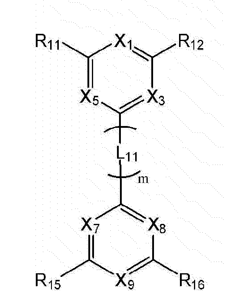
- Chemical Formula 2 may be represented by the following Chemical Formula 4.
- At least one of X 1 , X 3 , X 5 and X 7 to X 9 is N, and the others are CR 1 ,
- R 1 , R 11 , R 12 , R 15 and R 16 are the same as or different from each other, and are each a monovalent organic group
- L 11 is the same as or different from each other, is a divalent organic group, and m is an integer of 1 to 3,
- Adjacent monovalent organic groups or adjacent divalent organic groups may be bonded to each other to form a substituted or unsubstituted aliphatic ring or a substituted or unsubstituted aromatic ring.
- the second electron transport material is an organic material including a 5-membered heterocycle or cyano group including at least one hetero atom of N, O, and S.
- the second electron transport material does not include a six-membered heterocycle.
- the 5-membered hetero ring may be represented by the following Formula 5.
- Y 1 is NR 21 , O or S
- Y 2 to Y 5 are the same as or different from each other, and are each N or CR 22 ,
- R 21 and R 22 are the same as or different from each other, and are each a monovalent organic group
- Adjacent monovalent organic groups may be bonded to each other to form a substituted or unsubstituted aliphatic ring or a substituted or unsubstituted aromatic ring.
- the second electron transport material is an organic material including imidazole, oxazole or thiazole.
- Y 5 is CR 22 .
- Y 4 is CR 22 .
- Y 5 and Y 4 are each CR 22 , and R 22 may be bonded to each other to form a substituted or unsubstituted aliphatic ring or a substituted or unsubstituted aromatic ring.
- Y 5 and Y 4 are each CR 22 , and R 22 may be bonded to each other to form a substituted or unsubstituted aromatic ring.
- Y 5 and Y 4 are each CR 22 , and R 22 may be bonded to each other to form a substituted or unsubstituted benzene ring.
- the second electron transport material may be represented by the following formula (6).
- Y 1 is NR 21 , O or S
- Y 2 and Y 3 are the same as or different from each other, and are each N or CR 22 ,
- R 2 , R 21 and R 22 are the same as or different from each other, and are each a monovalent organic group
- n is an integer from 0 to 4,
- Adjacent monovalent organic groups may be bonded to each other to form a substituted or unsubstituted aliphatic ring or a substituted or unsubstituted aromatic ring.
- Y 2 is CR 22 .
- Chemical Formula 6 may be represented by the following Chemical Formula 7.
- Y 1 is NR 21 , O or S
- Y 3 is N or CR 22 ,
- R 2 , R 3 , R 21 and R 22 are the same as or different from each other, and are each a monovalent organic group
- n is an integer from 0 to 4,
- Adjacent monovalent organic groups may be bonded to each other to form a substituted or unsubstituted aliphatic ring or a substituted or unsubstituted aromatic ring.
- the second electron transport material is an organic material including benzimidazole, benzoxazole or benzothiazole.
- Y 1 is O.
- Y 1 is S.
- Y 1 is NR 21 .
- Y 3 is N.
- Chemical Formula 7 may be represented by any one of the following Chemical Formulas 8 to 10.
- R 2 , R 3 and R 4 are the same as or different from each other and are monovalent organic groups
- n is an integer from 0 to 4,
- Adjacent monovalent organic groups may be bonded to each other to form a substituted or unsubstituted aliphatic ring or a substituted or unsubstituted aromatic ring.
- Chemical Formula 7 may be represented by the following Chemical Formula 11.
- Y 1 is NR 21 , O or S
- Y 3 is N or CR 22 ,
- R 2 , R 5 , R 21 and R 22 are the same as or different from each other, and are each a monovalent organic group
- n is an integer from 0 to 4,
- Adjacent monovalent organic groups may be bonded to each other to form a substituted or unsubstituted aliphatic ring or a substituted or unsubstituted aromatic ring.
- Chemical Formula 7 may be represented by the following Chemical Formula 12.
- Y 1 and Y 6 are the same as or different from each other, and are each NR 21 , O, or S,
- Y 3 and Y 7 are the same as or different from each other, and are each N or CR 22 ,
- R 2 , R 6 , R 21 and R 22 are the same as or different from each other, and are each a monovalent organic group
- n and q are each an integer of 0 to 4,
- L 22 is the same as or different from each other, is a divalent organic group, and p is an integer of 1 to 3,
- Adjacent monovalent organic groups or adjacent divalent organic groups may be bonded to each other to form a substituted or unsubstituted aliphatic ring or a substituted or unsubstituted aromatic ring.
- Chemical Formula 7 may be represented by the following Chemical Formula 13.
- R 2 , R 7 and R 8 are the same as or different from each other, and are each a monovalent organic group
- n, r and s are each an integer of 0 to 4,
- Adjacent monovalent organic groups may be bonded to each other to form a substituted or unsubstituted aliphatic ring or a substituted or unsubstituted aromatic ring.
- the compound containing a cyano group as the second electron transport material may be represented by the following formula (14).
- L 31 is a divalent organic group
- t is an integer from 0 to 4, when t is 2 or more, L 31 is the same as or different from each other,
- R 31 is a monovalent organic group.
- L 31 includes a substituted or unsubstituted anthracene.
- Chemical Formula 14 may be represented by the following Chemical Formula 15.
- L 32 and L 33 are divalent organic groups, R 32 and R 33 are monovalent organic groups,
- x and y are each an integer of 0-4, z is an integer of 0-8, and when x, y or z is 2 or more, the structures in parentheses are the same or different from each other.
- L 32 is a phenylene group.
- L 33 is a phenylene group.
- Chemical Formula 15 may be represented by the following Chemical Formula 16.
- Examples of the organic group in the present specification include hydrogen, an alkyl group, an alkenyl group, a cycloalkyl group, a cycloalkenyl group, an aryl group, an aralkyl group, and the like.
- This organic group may contain the bond and substituents other than hydrocarbon groups, such as a hetero atom, in the said organic group.
- the organic group may be any of linear, branched and cyclic.
- the monovalent organic group means a monovalent group having one bonding position in an organic compound.
- a divalent organic group refers to a divalent group having two bonding positions in an organic compound.
- the organic group may form a cyclic structure, may form a cyclic structure, and may include a hetero atom to form a bond as long as the effects of the invention are not impaired.
- the bond containing hetero atoms such as an oxygen atom, a nitrogen atom, and a silicon atom, is mentioned.
- the cyclic structure may include the aforementioned aromatic ring, aliphatic ring, and the like, and may be monocyclic or polycyclic.
- the monovalent organic group is hydrogen; heavy hydrogen; Halogen group; Nitrile group; Nitro group; Hydroxyl group; Carbonyl group; Ester group; Imide group; Amide group; Substituted or unsubstituted alkyl group; A substituted or unsubstituted cycloalkyl group; Substituted or unsubstituted alkoxy group; Substituted or unsubstituted aryloxy group; Substituted or unsubstituted alkylthioxy group; Substituted or unsubstituted arylthioxy group; Substituted or unsubstituted alkyl sulfoxy group; Substituted or unsubstituted aryl sulfoxy group; Substituted or unsubstituted alkenyl group; Substituted or unsubstituted silyl group; Substituted
- the monovalent organic group may be a substituted or unsubstituted aryl group; Or a substituted or unsubstituted aromatic or aliphatic heterocyclic group.
- the monovalent organic group when the monovalent organic group is substituted, is a substituted or unsubstituted aryl group; And it may be substituted with one or more substituents selected from the group consisting of a substituted or unsubstituted aromatic or aliphatic heterocyclic group.
- the monovalent organic group when the monovalent organic group is substituted, is an aryl group; Dialkyl fluorenyl group; Spirobifluorenyl group; Carbazole groups; Benzocarbazole group; And it may be substituted with one or more substituents selected from the group consisting of aromatic or aliphatic heterocyclic group.
- the monovalent organic group is a phenyl group, a naphthyl group, a biphenyl group, a terphenyl group, a dialkyl fluorenyl group, a phenanthrenyl group, a spirobifluorenyl group, an anthracenyl group or a C 1-10 It may be an alkyl group, wherein the phenyl group, naphthyl group, biphenyl group, terphenyl group, dialkyl fluorenyl group, phenanthrenyl group, spirobifluorenyl group, anthracenyl group and an alkyl group having 1 to 10 carbon atoms are phenyl group, naphthyl group, bi Phenyl group, terphenyl group, dialkyl fluorenyl group, phenanthrenyl group, spirobifluorenyl group, anthracenyl group, pyridine
- the divalent organic group may be a substituted or unsubstituted arylene group; Or a substituted or unsubstituted aromatic or aliphatic divalent heterocyclic group.
- the divalent organic group when the divalent organic group is substituted, is a substituted or unsubstituted aryl group; And it may be substituted with one or more substituents selected from the group consisting of a substituted or unsubstituted aromatic or aliphatic heterocyclic group.
- the divalent organic group when the divalent organic group is substituted, is an aryl group; Dialkyl fluorenyl group; Spirobifluorenyl group; Carbazole groups; Benzocarbazole group; And it may be substituted with one or more substituents selected from the group consisting of aromatic or aliphatic heterocyclic group.
- the divalent organic group is a phenylene group, naphthylene group, biphenylylene group, terphenylene group, dialkyl fluorenylene group, phenanthrenylene group, spirobifluorenylene group, or Anthracenylene group
- the phenylene group, naphthylene group, biphenylylene group, terphenylene group, dialkyl fluorenylene group, phenanthrenylene group, spirobifluorenylene group, and anthracenylene group is a phenyl group, naphthyl group , Biphenyl group, terphenyl group, dialkyl fluorenyl group, phenanthrenyl group, spirobifluorenyl group, anthracenyl group, pyridine group, triazine group, quinoline group, carbazole group, benzocarbazole group, benzimidazole group, benzoxa Sub
- substituted means that a hydrogen atom bonded to a carbon atom of the compound is replaced with another substituent, and the position to be substituted is not limited to a position where the hydrogen atom is substituted, that is, a position where a substituent can be substituted, if two or more substituted , Two or more substituents may be the same or different from each other.
- substituted or unsubstituted is deuterium; Halogen group; Nitrile group; Nitro group; Imide group; Amide group; Hydroxyl group; Substituted or unsubstituted alkyl group; A substituted or unsubstituted cycloalkyl group; Substituted or unsubstituted alkoxy group; Substituted or unsubstituted alkenyl group; Substituted or unsubstituted amine group; Substituted or unsubstituted aryl group; And it is substituted with one or two or more substituents selected from the group consisting of a substituted or unsubstituted heterocyclic group, or two or more of the substituents exemplified above are substituted with a substituent, or means that do not have any substituents.
- a substituent to which two or more substituents are linked may be a biphenyl group. That is, the biphenyl group may be an aryl group or may be interpreted as a substituent to which two phenyl groups are linked.
- examples of the halogen group include fluorine, chlorine, bromine or iodine.
- the oxygen of the ester group may be substituted with a linear, branched or cyclic alkyl group having 1 to 25 carbon atoms or an aryl group having 6 to 25 carbon atoms. Specifically, it may be a compound of the following structural formula, but is not limited thereto.
- carbon number of an imide group is not specifically limited, It is preferable that it is C1-C25. Specifically, it may be a compound having a structure as follows, but is not limited thereto.
- the amide group may be substituted with one or two of the nitrogen of the amide group is hydrogen, a linear, branched or cyclic alkyl group having 1 to 25 carbon atoms or an aryl group having 6 to 25 carbon atoms. Specifically, it may be a compound of the following structural formula, but is not limited thereto.
- the alkyl group may be linear or branched chain, carbon number is not particularly limited, but is preferably 1 to 50.
- Specific examples include methyl, ethyl, propyl, n-propyl, isopropyl, butyl, n-butyl, isobutyl, tert-butyl, sec-butyl, 1-methyl-butyl, 1-ethyl-butyl, pentyl, n-pentyl , Isopentyl, neopentyl, tert-pentyl, hexyl, n-hexyl, 1-methylpentyl, 2-methylpentyl, 4-methyl-2-pentyl, 3,3-dimethylbutyl, 2-ethylbutyl, heptyl, n -Heptyl, 1-methylhexyl, cyclopentylmethyl, cyclohexylmethyl, octyl, n-o
- the cycloalkyl group is not particularly limited, but preferably 3 to 60 carbon atoms, specifically, cyclopropyl, cyclobutyl, cyclopentyl, 3-methylcyclopentyl, 2,3-dimethylcyclopentyl, cyclohexyl, 3-methylcyclohexyl, 4-methylcyclohexyl, 2,3-dimethylcyclohexyl, 3,4,5-trimethylcyclohexyl, 4-tert-butylcyclohexyl, cycloheptyl, cyclooctyl, and the like, but are not limited thereto. Do not.
- the alkoxy group may be linear, branched or cyclic. Although carbon number of an alkoxy group is not specifically limited, It is preferable that it is C1-C20. Specifically, methoxy, ethoxy, n-propoxy, isopropoxy, i-propyloxy, n-butoxy, isobutoxy, tert-butoxy, sec-butoxy, n-pentyloxy, neopentyloxy, Isopentyloxy, n-hexyloxy, 3,3-dimethylbutyloxy, 2-ethylbutyloxy, n-octyloxy, n-nonyloxy, n-decyloxy, benzyloxy, p-methylbenzyloxy and the like It may be, but is not limited thereto.
- the alkenyl group may be linear or branched chain, the carbon number is not particularly limited, but is preferably 2 to 40.
- Specific examples include vinyl, 1-propenyl, isopropenyl, 1-butenyl, 2-butenyl, 3-butenyl, 1-pentenyl, 2-pentenyl, 3-pentenyl, 3-methyl-1- Butenyl, 1,3-butadienyl, allyl, 1-phenylvinyl-1-yl, 2-phenylvinyl-1-yl, 2,2-diphenylvinyl-1-yl, 2-phenyl-2- ( Naphthyl-1-yl) vinyl-1-yl, 2,2-bis (diphenyl-1-yl) vinyl-1-yl, stilbenyl group, styrenyl group and the like, but are not limited thereto.
- the aryl group is a monocyclic aryl group
- carbon number is not particularly limited, but preferably 6 to 25 carbon atoms.
- the monocyclic aryl group may be a phenyl group, a biphenyl group, a terphenyl group, etc., but is not limited thereto.
- Carbon number is not particularly limited when the aryl group is a polycyclic aryl group. It is preferable that it is C10-24.
- the polycyclic aryl group may be naphthyl group, anthryl group, phenanthryl group, pyrenyl group, perylenyl group, chrysenyl group, fluorenyl group, etc., but is not limited thereto.
- the fluorenyl group may be substituted, and adjacent substituents may be bonded to each other to form a ring.
- the silyl group includes trimethylsilyl group, triethylsilyl group, t-butyldimethylsilyl group, vinyldimethylsilyl group, propyldimethylsilyl group, triphenylsilyl group, diphenylsilyl group, phenylsilyl group, and the like.
- the present invention is not limited thereto.
- the amine group is not particularly limited, but is preferably 1 to 30.
- Specific examples of the amine group include methylamine group, dimethylamine group, ethylamine group, diethylamine group, phenylamine group, naphthylamine group, biphenylamine group, anthracenylamine group, and 9-methyl-anthracenylamine group.
- examples of the arylamine group include a substituted or unsubstituted monoarylamine group, a substituted or unsubstituted diarylamine group, or a substituted or unsubstituted triarylamine group.
- the aryl group in the arylamine group may be a monocyclic aryl group, may be a polycyclic aryl group.
- the arylamine group including two or more aryl groups may simultaneously include a monocyclic aryl group, a polycyclic aryl group, or a monocyclic aryl group and a polycyclic aryl group.
- aryl amine group examples include phenylamine, naphthylamine, biphenylamine, anthracenylamine, 3-methyl-phenylamine, 4-methyl-naphthylamine, 2-methyl-biphenylamine, 9-methyl-anthra Cenylamine, diphenyl amine group, phenyl naphthyl amine group, ditolyl amine group, phenyl tolyl amine group, carbazole and triphenyl amine group and the like, but are not limited thereto.
- examples of the arylphosphine group include a substituted or unsubstituted monoarylphosphine group, a substituted or unsubstituted diarylphosphine group, or a substituted or unsubstituted triarylphosphine group.
- the aryl group in the arylphosphine group may be a monocyclic aryl group, may be a polycyclic aryl group.
- the arylphosphine group containing two or more aryl groups may simultaneously include a monocyclic aryl group, a polycyclic aryl group, or a monocyclic aryl group and a polycyclic aryl group.
- the heterocyclic group includes one or more atoms other than carbon and heteroatoms, and specifically, the heteroatoms may include one or more atoms selected from the group consisting of O, N, Se, and S, and the like.
- carbon number is not specifically limited, It is preferable that it is C2-C60.
- heterocyclic group examples include thiophene group, furan group, pyrrole group, imidazole group, thiazole group, oxazole group, oxadiazole group, pyridyl group, bipyridyl group, pyrimidyl group, triazine group, triazole group, acridil group , Pyridazine group, pyrazinyl group, quinolinyl group, quinazoline group, quinoxalinyl group, phthalazinyl group, pyrido pyrimidinyl group, pyrido pyrazinyl group, pyrazino pyrazinyl group, isoquinoline group, indole group , Carbazole group, benzoxazole group, benzoimidazole group, benzothiazole group, benzocarbazole group, benzothiophene group, dibenzothiophene group, benzofuranyl group, phenanthro
- the aryl group in the aryloxy group, arylthioxy group, aryl sulfoxy group and aralkylamine group is the same as the aryl group described above.
- the aryloxy group phenoxy, p-tolyloxy, m-tolyloxy, 3,5-dimethyl-phenoxy, 2,4,6-trimethylphenoxy, p-tert-butylphenoxy, 3-biphenyl Oxy, 4-biphenyloxy, 1-naphthyloxy, 2-naphthyloxy, 4-methyl-1-naphthyloxy, 5-methyl-2-naphthyloxy, 1-anthryloxy, 2-anthryl Oxy, 9-anthryloxy, 1-phenanthryloxy, 3-phenanthryloxy, 9-phenanthryloxy, and the like.
- arylthioxy group examples include a phenylthioxy group, 2-methylphenylthioxy group, and 4-tert-butylphenyl.
- Thioxy groups and the like, and aryl sulfoxy groups include, but are not limited to, benzene sulfoxy groups and p-toluene sulfoxy groups.
- the alkyl group in the alkyl thioxy group and the alkyl sulfoxy group is the same as the example of the alkyl group mentioned above.
- the alkyl thioxy group includes a methyl thioxy group, an ethyl thioxy group, a tert-butyl thioxy group, a hexyl thioxy group, an octyl thioxy group
- the alkyl sulfoxy group includes mesyl, ethyl sulfoxy, propyl sulfoxy and butyl sulfoxy Etc., but is not limited thereto.
- the first electron transport material may be selected from one or two or more of the organic material represented by the formulas cp6-1 to cp6-24.
- the second electron transport material may be selected from one or two or more of the organic material represented by the formulas cp7-1 to cp7-21.
- the dipole moment values of some of the compounds are as follows.
- the first electron transport material and the second electron transport material have a molecular weight of 400 Da to 900 Da, respectively.
- the first electron transport material and the second electron transport material in the electron transport layer may be used in a volume ratio of 1:99 to 99: 1.
- the first electron transport material and the second electron transport material in the electron transport layer may be used in a volume ratio of 1: 9 to 9: 1.
- the first electron transport material and the second electron transport material are 1: 9, 2: 8, 3: 7, 4: 6, 5: 5, 6: 4, 7: 3, 8: 2, Or in a volume ratio of 9: 1.
- the first electron transport material and the second electron transport material in the electron transport layer may be used in a volume ratio of 1: 9 to 5: 5.
- the second electron transport material according to the exemplary embodiment of the present specification has better electron injection and / or electron transport characteristics than the first electron transport material. However, even when the electron injection and electron transport characteristics are excellent, the hole and the electron are balanced, that is, the closer the ratio of the electron and the hole to 1, the generation of excitons increases, thereby maximizing the efficiency characteristics of the device.
- the amount of electrons transferred to the light emitting layer is required to adjust the amount of electrons transferred to the light emitting layer, which may be performed by adjusting the ratio of the first electron transport material and the second electron transport material as described above. Therefore, in the case of having a volume ratio of the first electron transport material and the second electron transport material according to an exemplary embodiment of the present specification, the amount of electrons transferred from the electron transport layer to the light emitting layer is appropriately adjusted to improve the high luminous efficiency of the device. You can expect
- the organic electroluminescent device further comprises an electron injection layer provided between the electron transport layer and the cathode.
- the organic electroluminescent device of the present specification may further include one or more organic material layers between the anode and the light emitting layer.
- the organic electroluminescent device of the present specification may further include one or more organic material layers between the light emitting layer and the electron transport layer and / or between the electron transport layer and the cathode.
- the organic EL device of the present specification may have a structure including a hole injection layer, a hole transport layer, a light emitting layer, an electron transport layer, an electron injection layer and the like as an organic material layer.
- the structure of the organic electroluminescent device is not limited thereto and may include a smaller number of organic layers. Although one example is illustrated in FIG. 1, the present invention is not limited thereto, and the organic EL device may include a smaller number of organic layers or may further include additional organic layers.
- the organic EL device may be an organic EL device having a structure in which an anode, an organic material layer, and a cathode are sequentially stacked on a substrate.
- the organic electroluminescent device may be an organic electroluminescent device of an inverted type in which a cathode, one or more organic material layers, and an anode are sequentially stacked on a substrate.
- the organic light emitting device of the present specification may be manufactured by materials and methods known in the art, except that the electron transport layer of the organic material layer includes the first electron transport material and the second electron transport material.
- the electron transport layer may contain additional compounds in addition to the two kinds.
- the organic EL device of the present specification may be manufactured by sequentially stacking a first electrode, an organic material layer, and a second electrode on a substrate.
- the anode is formed by depositing a metal or conductive metal oxide or an alloy thereof on the substrate by using a physical vapor deposition (PVD) method such as sputtering or e-beam evaporation.
- PVD physical vapor deposition
- an organic material layer including a hole injection layer, a hole transporting layer, a light emitting layer, and an electron transporting layer thereon, and then depositing a material that can be used as a cathode thereon.
- an organic EL device may be manufactured by sequentially depositing a cathode material, an organic material layer, and an anode material on a substrate.
- the organic material layer may be formed by a solution coating method as well as a vacuum deposition method in the manufacture of the organic EL device.
- the solution coating method means spin coating, dip coating, doctor blading, inkjet printing, screen printing, spray method, roll coating, etc., but is not limited thereto.
- the first electrode is a cathode
- the second electrode is an anode
- the first electrode is an anode
- the second electrode is a cathode
- the substrate may be selected in consideration of optical and physical properties as needed.
- the substrate is preferably transparent.
- the substrate may be a hard material, but may be made of a flexible material such as plastic.
- the substrate may be made of polyethylene terephthalate (PET), polyethylene naphthalate (PEN), polypropylene (PP), polyimide (PI), polycarbonate (PC), polystyrene (PS), polyoxymethylene (POM), and AS resin ( acrylonitrile styrene copolymer), ABS resin (acrylonitrile butadiene styrene copolymer), TAC (Triacetyl cellulose) and PAR (polyarylate) and the like, but are not limited thereto.
- PET polyethylene terephthalate
- PEN polyethylene naphthalate
- PP polypropylene
- PI polyimide
- PC polycarbonate
- PS polystyrene
- POM polyoxymethylene
- AS resin acrylonitrile styrene copolymer
- ABS resin acrylonitrile butadiene styrene copolymer
- TAC Triacetyl cellulose
- PAR polyarylate
- the cathode material is generally a material having a small work function to facilitate electron injection into the organic material layer.
- Specific examples of the cathode materials include metals such as magnesium, calcium, sodium, potassium, titanium, indium, yttrium, lithium, gadolinium, aluminum, silver, tin and lead or alloys thereof; Multilayer structure materials such as LiF / Al or LiO 2 / Al, and the like, but are not limited thereto.
- anode material a material having a large work function is generally preferred to facilitate hole injection into the organic material layer.
- anode materials that can be used herein include metals such as vanadium, chromium, copper, zinc, gold or alloys thereof; Metal oxides such as zinc oxide, indium oxide, indium tin oxide (ITO), indium zinc oxide (IZO); ZnO: Al or SnO 2 : Combination of metals and oxides such as Sb; Conductive polymers such as poly (3-methylthiophene), poly [3,4- (ethylene-1,2-dioxy) thiophene] (PEDOT), polypyrrole and polyaniline, and the like, but are not limited thereto.
- the hole transport layer is a layer that receives holes from the hole injection layer and transports holes to the light emitting layer.
- the hole transport material is a material capable of transporting holes from the anode or the hole injection layer to the light emitting layer.
- the material is suitable. Specific examples thereof include an arylamine-based organic material, a conductive polymer, and a block copolymer having a conjugated portion and a non-conjugated portion together, but are not limited thereto.
- the hole injection layer is a layer for injecting holes from the electrode, and has a capability of transporting holes to the hole injection material, has an effect of hole injection at the anode, excellent hole injection effect to the light emitting layer or the light emitting material, and produced in the light emitting layer
- the compound which prevents the excitons from moving to the electron injection layer or the electron injection material, and is excellent in thin film formation ability is preferable.
- the hole injection material preferably has a higher occupied molecular orbital (HOMO) between the work function of the anode material and the HOMO of the surrounding organic material layer.
- the hole injection material examples include metal porphyrin, oligothiophene, arylamine-based organics, phthalocyanine derivatives, hexanitrile hexaazatriphenylene-based organics, quinacridone-based organics, Perylene-based organic material, anthraquinone and polyaniline and polythiophene-based conductive polymers, but are not limited thereto.
- the light emitting material is a material capable of emitting light in the visible region by transporting and combining holes and electrons from the hole transport layer and the electron transport layer, respectively, and a material having good quantum efficiency with respect to fluorescence or phosphorescence is preferable.
- Specific examples thereof include 8-hydroxyquinoline aluminum complex (Alq 3 ); Carbazole series compounds; Dimerized styryl compounds; BAlq; 10-hydroxybenzoquinoline-metal compound; Benzoxazole, benzthiazole and benzimidazole series compounds; Poly (p-phenylenevinylene) (PPV) -based polymers; Spiro compounds; Polyfluorene, rubrene and the like, but are not limited thereto.
- the light emitting layer may include a host material and a dopant material.
- the host material is a condensed aromatic ring derivative or a heterocyclic containing compound.
- the condensed aromatic ring derivatives include anthracene derivatives, pyrene derivatives, naphthalene derivatives, pentacene derivatives, phenanthrene compounds, and fluoranthene compounds
- the heterocyclic containing compounds include carbazole derivatives, dibenzofuran derivatives and ladder types. Furan compounds, pyrimidine derivatives, and the like, but are not limited thereto.
- Dopant materials include aromatic amine derivatives, styrylamine compounds, boron complexes, fluoranthene compounds, metal complexes, and the like.
- the aromatic amine derivatives include condensed aromatic ring derivatives having a substituted or unsubstituted arylamino group, and include pyrene, anthracene, chrysene, and periplanthene having an arylamino group, and a styrylamine compound may be substituted or unsubstituted.
- At least one arylvinyl group is substituted with the substituted arylamine, and one or two or more substituents selected from the group consisting of an aryl group, a silyl group, an alkyl group, a cycloalkyl group and an arylamino group are substituted or unsubstituted.
- substituents selected from the group consisting of an aryl group, a silyl group, an alkyl group, a cycloalkyl group and an arylamino group are substituted or unsubstituted.
- the metal complex includes, but is not limited to, an iridium complex, a platinum complex, and the like.
- the electron injection layer is a layer that injects electrons from an electrode, has an ability to transport electrons, has an electron injection effect from a cathode, an electron injection effect with respect to a light emitting layer or a light emitting material, and hole injection of excitons generated in the light emitting layer
- the compound which prevents the movement to a layer and is excellent in thin film formation ability is preferable.
- fluorenone anthraquinodimethane, diphenoquinone, thiopyran dioxide, oxazole, oxadiazole, triazole, imidazole, perylenetetracarboxylic acid, preorenylidene methane, anthrone and the like and derivatives thereof, metal Complex compounds, nitrogen-containing five-membered ring derivatives, and the like, but are not limited thereto.
- a transparent electrode (Indium Tin Oxide) was deposited to a thickness of 100 nm using a hole injection electrode on a glass substrate, and oxygen plasma treatment was performed for 30 sec at 80 w at 30 mtorr pressure.
- [Cp1] was deposited to a thickness of 30 nm by applying heat in a vacuum.
- [Cp2] was deposited to a thickness of 800 nm as a hole injection and transport layer thereon.
- [Cp3] was deposited to a thickness of 200 nm on the hole transport layer.
- [Cp4] was deposited to a thickness of 20 nm with a light emitting layer and 4% doped with [cp5] by volume with a light emitting dopant.
- An organic light emitting device was fabricated by depositing [cp6-22] at a thickness of 30 nm, depositing LiF at a thickness of 1 nm with an electron injection layer thereon, and depositing aluminum (Al) at a thickness of 150 nm with an electron injection electrode thereon. It was.
- the dipole moments of the compounds A-1, A-2 and B-1 to B-3 are shown in Table 5 below.
- the dipole moment values of the compounds B-1 to B-3 corresponding to the first electron transport material including the N-containing six-membered ring as in Comparative Examples 3-1 to 3-4 are N
- the dipole moment value of the compounds A-1 and A-2 corresponding to the second electron transport material including a five-membered heterocycle including at least one hetero element of O and S is described in Table 4 of the present invention
- Table 4 the dipole moment value of the compounds A-1 and A-2 corresponding to the second electron transport material including a five-membered heterocycle including at least one hetero element of O and S
- the dipole moment value of the second electron transport material including a 5-membered heterocycle or cyano group including at least one hetero atom of N, O, and S is an N-containing 6-membered ring.
- the transport capacity of the electron transport layer containing the first electron transport material and the second electron transport material is increased, Low driving voltage and high efficiency can be expected.
Landscapes
- Chemical & Material Sciences (AREA)
- Organic Chemistry (AREA)
- Physics & Mathematics (AREA)
- Engineering & Computer Science (AREA)
- Materials Engineering (AREA)
- Spectroscopy & Molecular Physics (AREA)
- Optics & Photonics (AREA)
- Electroluminescent Light Sources (AREA)
- Plural Heterocyclic Compounds (AREA)
Abstract
Description


| 화합물 | 쌍극자 모멘트 | 화합물 | 쌍극자 모멘트 |
| cp6-1 | 0.44 | cp7-1 | 3.75 |
| cp6-2 | 0.45 | cp7-2 | 3.67 |
| cp6-3 | 0.32 | cp7-3 | 1.56 |
| cp6-4 | 1.43 | cp7-4 | 4.46 |
| Cp6-5 | 0.20 | cp7-5 | 1.52 |
| cp6-8 | 1.71 | cp7-17 | 3.13 |
| cp6-10 | 1.76 | cp7-19 | 5.13 |
| cp6-13 | 2.54 | cp7-20 | 5.72 |
| cp6-22 | 1.01 |

| 화학식 | V | Cd/A | 수명(hour) | |
| 비교예 1-1 | Cp6-1 | 5.93 | 4.13 | 2 |
| 비교예 1-2 | Cp6-2 | 4.86 | 4.02 | 13 |
| 비교예 1-3 | Cp6-3 | 5.12 | 3.79 | 21 |
| 비교예 1-4 | Cp6-4 | 5.64 | 3.8 | 25 |
| 비교예 1-5 | Cp6-5 | 5.26 | 4.2 | 3 |
| 비교예 1-6 | Cp6-13 | 5.38 | 4.01 | 32 |
| 비교예 1-7 | Cp6-22 | 5.59 | 3.38 | 28 |
| 화학식 | V | Cd/A | 수명 | |
| 비교예 2-1 | Cp7-1 | 3.6 | 4.2 | 30 |
| 비교예 2-2 | Cp7-2 | 3.7 | 4.3 | 9 |
| 비교예 2-3 | Cp7-3 | 3.9 | 3.9 | 4.2 |
| 비교예 2-4 | Cp7-4 | 3.7 | 5.39 | 1.2 |
| 비교예 2-5 | Cp7-5 | 4.0 | 3.9 | 8.4 |
| 비교예 2-6 | Cp7-19 | 3.6 | 4.6 | 7.3 |
| 화학식 | V | Cd/A | 수명 | |
| 실시예 1-1 | Cp6-1 & cp7-1 | 3.6 | 4.9 | 40 |
| 실시예 1-2 | Cp6-1 & cp7-2 | 3.8 | 4.8 | 15 |
| 실시예 1-3 | Cp6-1 & cp7-3 | 3.6 | 4.95 | 28 |
| 실시예 1-4 | Cp6-1 & cp7-4 | 3.74 | 5.56 | 14 |
| 실시예 1-5 | Cp6-1 & cp7-5 | 4.0 | 4.5 | 23 |
| 실시예 1-6 | Cp6-2 & cp7-1 | 3.9 | 4.1 | 87 |
| 실시예 1-7 | Cp6-2 & cp7-2 | 4.0 | 3.9 | 45 |
| 실시예 1-8 | Cp6-2 & cp7-3 | 3.9 | 4.4 | 66 |
| 실시예 1-9 | Cp6-2 & cp7-4 | 4.1 | 4.0 | 67 |
| 실시예 1-10 | Cp6-2 & cp7-5 | 4.1 | 4.2 | 51 |
| 실시예 1-11 | Cp6-3 & cp7-1 | 4.04 | 3.9 | 105 |
| 실시예 1-12 | Cp6-3 & cp7-2 | 4.2 | 3.7 | 47 |
| 실시예 1-13 | Cp6-3 & cp7-3 | 4.2 | 4.1 | 82 |
| 실시예 1-14 | Cp6-3 & cp7-4 | 4.2 | 4.0 | 70 |
| 실시예 1-15 | Cp6-3 & cp7-5 | 4.1 | 3.9 | 45 |
| 실시예 1-16 | Cp6-4 & cp7-1 | 3.8 | 4.5 | 63 |
| 실시예 1-17 | Cp6-4 & cp7-2 | 3.9 | 4.3 | 37 |
| 실시예 1-18 | Cp6-4 & cp7-3 | 4.0 | 4.3 | 42 |
| 실시예 1-19 | Cp6-4 & cp7-4 | 3.9 | 4.6 | 33 |
| 실시예 1-20 | Cp6-4 & cp7-5 | 4.1 | 4.2 | 47 |
| 실시예 1-21 | Cp6-5 & cp7-1 | 4.0 | 4.6 | 56 |
| 실시예 1-22 | Cp6-5 & cp7-2 | 4.2 | 4.4 | 28 |
| 실시예 1-23 | Cp6-5 & cp7-3 | 4.1 | 4.5 | 35 |
| 실시예 1-24 | Cp6-5 & cp7-4 | 4.3 | 4.2 | 21 |
| 실시예 1-25 | Cp6-5 & cp7-5 | 4.4 | 3.9 | 22 |
| 실시예 1-26 | Cp6-22 & cp7-19 | 4.0 | 4.6 | 62 |
| 실시예 1-27 | Cp6-13 & cp7-19 | 4.4 | 4.2 | 82 |

| 화합물 | 쌍극자 모멘트 |
| A-1 | 2.70 |
| A-2 | 2.63 |
| B-1 | 3.31 |
| B-2 | 3.80 |
| B-3 | 4.58 |
| 화학식 | V | Cd/A | 수명 | |
| 비교예 3-1 | 화합물 A-1 & 화합물 B-1 | 5.0 | 4.0 | 16 |
| 비교예 3-2 | 화합물 A-1 & 화합물 B-2 | 5.1 | 3.9 | 17 |
| 비교예 3-3 | 화합물 A-2 & 화합물 B-1 | 5.3 | 4.2 | 15 |
| 비교예 3-4 | 화합물 A-2 & 화합물 B-3 | 5.5 | 4.1 | 20 |
| 화학식 | V | Cd/A | 수명 | |
| 비교예 4-1 | Cp6-1 (20nm) / cp7-2(10nm) | 4.4 | 4.2 | 12 |
| 비교예 4-2 | Cp6-4 (20nm) / cp7-5 (10nm) | 4.4 | 3.9 | 16 |
| 비교예 4-3 | Cp7-2 (20nm) / cp6-1 (10nm) | 6.2 | 2.9 | 6 |
| 비교예 4-4 | Cp7-5 (20nm) / cp6-4 (10nm) | 5.9 | 3.1 | 5 |
Claims (13)
- 애노드;캐소드;상기 애노드와 상기 캐소드 사이에 구비된 발광층; 및상기 캐소드와 상기 발광층 사이에 구비된 전자수송층을 포함하고,상기 전자수송층은 제1 전자수송물질 및 제2 전자수송물질을 포함하며,상기 제1 전자수송물질은 N 함유 6원 고리를 포함하는 단환 또는 다환의 고리를 포함하는 유기물이고,상기 제2 전자수송물질은 N, O 및 S 중 적어도 하나의 이종원소를 포함하는 5원 헤테로고리 또는 시아노기를 포함하는 유기물이며,상기 제2 전자수송물질의 쌍극자 모멘트(dipole moment)가 상기 제1 전자수송물질의 쌍극자 모멘트에 비하여 더 큰 것인 유기 전계 발광 소자.
- 청구항 1에 있어서,상기 제1 전자수송물질의 쌍극자 모멘트는 0 Debye 내지 3 Debye 이고,상기 제2 전자수송물질의 쌍극자 모멘트는 1 Debye 내지 7 Debye인 것인 유기 전계 발광 소자.
- 청구항 1에 있어서,상기 제1 전자수송물질은 하기 화학식 1로 표시되는 구조를 포함하는 것인 유기 전계 발광 소자:[화학식 1]
 상기 화학식에 있어서,X1 내지 X6 중 1 내지 3개는 N이고,나머지는 CR1이며, R1은 1가 유기기이고,인접한 1가 유기기는 서로 결합하여 치환 또는 비치환된 지방족고리 또는 치환 또는 비치환된 방향족고리를 형성할 수 있다.
 - 청구항 1에 있어서,상기 제1 전자수송물질은 피리딘, 피리미딘 또는 트리아진을 포함하는 유기물인 것인 유기 전계 발광 소자.
- 청구항 1에 있어서,상기 제2 전자수송물질은 하기 화학식 5로 표시되는 구조를 포함하는 것인 유기 전계 발광 소자:[화학식 5]
 상기 화학식에 있어서,Y1은 NR21, O 또는 S이고,Y2 내지 Y5는 서로 같거나 상이하고, 각각 N 또는 CR22이며,R21 및 R22는 서로 같거나 상이하고 각각 1가 유기기이고,인접한 1가 유기기는 서로 결합하여 치환 또는 비치환된 지방족고리 또는 치환 또는 비치환된 방향족고리를 형성할 수 있다.
 - 청구항 1에 있어서,상기 제2 전자수송물질은 이미다졸, 옥사졸 또는 티아졸을 포함하는 유기물인 것인 유기 전계 발광 소자.
- 청구항 1에 있어서,상기 제2 전자수송물질은 벤즈이미다졸, 벤즈옥사졸 또는 벤조티아졸을 포함하는 유기물인 것인 유기 전계 발광 소자.
- 청구항 1에 있어서,상기 제2 전자수송물질은 하기 화학식 14로 표시되는 구조를 포함하는 것인 유기 전계 발광 소자:[화학식 14]CN-(L31)t-R31상기 화학식 14에 있어서,L31은 2가 유기기이고, t는 0 내지 4의 정수이며, t가 2 이상인 경우 L31은 서로 같거나 상이하고,R31은 1가 유기기이다.
- 청구항 1에 있어서,상기 제1 전자수송물질 및 상기 제2 전자수송물질은 금속 원소 또는 금속 착체를 포함하지 아니하는 것인 유기 전계 발광 소자.
- 청구항 1에 있어서,상기 제1 전자수송물질 및 상기 제2 전자수송물질은 금속 착체를 포함하지 아니하는 것인 유기 전계 발광 소자.
- 청구항 1에 있어서,상기 제1 전자수송물질 및 상기 제2 전자수송물질은 각각 분자량이 400 Da 내지 900 Da인 것인 유기 전계 발광 소자.
- 청구항 1에 있어서,상기 제1 전자수송물질과 제2 전자수송물질을 포함하는 전자수송층은상기 제1 전자수송물질과 상기 제2 전자수송물질을 1:99 내지 99:1의 부피비로 포함하는 것인 유기 전계 발광 소자.
- 청구항 1에 있어서,상기 유기 전계 발광 소자는 상기 전자수송층과 상기 캐소드 사이에 구비된 전자주입층을 더 포함하는 것인 유기 전계 발광 소자.
Priority Applications (4)
| Application Number | Priority Date | Filing Date | Title |
|---|---|---|---|
| JP2017511845A JP6457069B2 (ja) | 2014-10-27 | 2015-10-27 | 有機電界発光素子 |
| CN201580051461.4A CN106716665B9 (zh) | 2014-10-27 | 2015-10-27 | 有机电致发光器件 |
| US15/509,178 US10074809B2 (en) | 2014-10-27 | 2015-10-27 | Electron transport materials with selected dipole moments |
| EP15855213.3A EP3214151B1 (en) | 2014-10-27 | 2015-10-27 | Organic electroluminescence device |
Applications Claiming Priority (2)
| Application Number | Priority Date | Filing Date | Title |
|---|---|---|---|
| KR20140146402 | 2014-10-27 | ||
| KR10-2014-0146402 | 2014-10-27 |
Publications (1)
| Publication Number | Publication Date |
|---|---|
| WO2016068585A1 true WO2016068585A1 (ko) | 2016-05-06 |
Family
ID=55857827
Family Applications (1)
| Application Number | Title | Priority Date | Filing Date |
|---|---|---|---|
| PCT/KR2015/011393 Ceased WO2016068585A1 (ko) | 2014-10-27 | 2015-10-27 | 유기 전계 발광 소자 |
Country Status (7)
| Country | Link |
|---|---|
| US (1) | US10074809B2 (ko) |
| EP (1) | EP3214151B1 (ko) |
| JP (2) | JP6457069B2 (ko) |
| KR (2) | KR20160049500A (ko) |
| CN (1) | CN106716665B9 (ko) |
| TW (1) | TWI577070B (ko) |
| WO (1) | WO2016068585A1 (ko) |
Cited By (4)
| Publication number | Priority date | Publication date | Assignee | Title |
|---|---|---|---|---|
| CN108218802A (zh) * | 2016-12-14 | 2018-06-29 | 株式会社Lg化学 | 有机发光元件 |
| WO2018139662A1 (ja) * | 2017-01-30 | 2018-08-02 | 出光興産株式会社 | 有機エレクトロルミネッセンス素子及び電子機器 |
| USRE47654E1 (en) | 2010-01-15 | 2019-10-22 | Idemitsu Koasn Co., Ltd. | Organic electroluminescence device |
| US10934268B2 (en) | 2015-12-23 | 2021-03-02 | Lg Chem, Ltd. | Compound and organic electronic device comprising same |
Families Citing this family (35)
| Publication number | Priority date | Publication date | Assignee | Title |
|---|---|---|---|---|
| EP2545964A1 (en) | 2011-07-13 | 2013-01-16 | Phenex Pharmaceuticals AG | Novel FXR (NR1H4) binding and activity modulating compounds |
| WO2016068585A1 (ko) * | 2014-10-27 | 2016-05-06 | 주식회사 엘지화학 | 유기 전계 발광 소자 |
| KR101560102B1 (ko) * | 2014-11-20 | 2015-10-13 | 주식회사 엘지화학 | 유기 발광 소자 |
| CN105399696B (zh) * | 2015-12-25 | 2019-12-24 | 上海天马有机发光显示技术有限公司 | 有机电致发光化合物及其有机光电装置 |
| JP6659067B2 (ja) * | 2016-02-18 | 2020-03-04 | 出光興産株式会社 | 有機エレクトロルミネッセンス素子及び電子機器 |
| CA3252823A1 (en) | 2016-06-13 | 2025-02-25 | Gilead Sciences, Inc. | Substituted tert-butyl-3-(2-chloro-phenyl)-3-hydroxyazetidine-1-carboxylate compounds |
| MX385718B (es) | 2016-06-13 | 2025-03-18 | Gilead Sciences Inc | Compuestos moduladores de fxr (nr1h4). |
| KR20180041603A (ko) | 2016-10-14 | 2018-04-24 | 주식회사 엘지화학 | 유기전계 발광 소자 |
| KR102044427B1 (ko) * | 2016-12-14 | 2019-11-14 | 주식회사 엘지화학 | 유기 발광 소자 |
| KR102145024B1 (ko) * | 2016-12-20 | 2020-08-14 | 주식회사 엘지화학 | 유기 발광 소자 |
| KR102454951B1 (ko) * | 2017-01-16 | 2022-10-17 | 삼성전자주식회사 | 유기 발광 소자 |
| PT3600309T (pt) | 2017-03-28 | 2022-10-03 | Gilead Sciences Inc | Combinações terapêuticas para o tratamento de doenças hepáticas |
| EP3477720B1 (en) | 2017-03-30 | 2020-03-18 | LG Chem, Ltd. | Organic light emitting element |
| CN107805248A (zh) * | 2017-11-01 | 2018-03-16 | 长春海谱润斯科技有限公司 | 一种含有苯并咪唑结构的衍生物及其制备方法和有机电致发光器件 |
| KR102478677B1 (ko) | 2017-12-29 | 2022-12-16 | 엘지디스플레이 주식회사 | 유기 발광 소자 및 이를 이용한 유기 발광 표시 장치 |
| CN111247650B (zh) | 2018-02-02 | 2023-11-07 | 株式会社Lg化学 | 有机发光二极管 |
| KR102840359B1 (ko) * | 2018-02-20 | 2025-07-29 | 이데미쓰 고산 가부시키가이샤 | 유기 일렉트로루미네센스 소자 및 전자 기기 |
| KR101966306B1 (ko) * | 2018-06-18 | 2019-04-05 | 주식회사 엘지화학 | 유기 발광 소자 |
| CN108963098B (zh) * | 2018-08-03 | 2020-04-28 | 京东方科技集团股份有限公司 | 一种qled显示面板及其制备方法、显示装置 |
| CN112005393B (zh) * | 2018-09-03 | 2024-06-25 | 株式会社Lg化学 | 有机发光器件 |
| WO2020050585A1 (ko) * | 2018-09-03 | 2020-03-12 | 주식회사 엘지화학 | 유기 발광 소자 |
| JP2022017601A (ja) * | 2018-09-07 | 2022-01-26 | 出光興産株式会社 | 有機エレクトロルミネッセンス素子及び電子機器 |
| KR102225970B1 (ko) * | 2018-09-17 | 2021-03-10 | 주식회사 엘지화학 | 유기 발광 소자 |
| EP3911647B1 (en) | 2019-01-15 | 2023-12-13 | Gilead Sciences, Inc. | Isoxazole compound as fxr agonist and pharmaceutical compositions comprising same |
| KR102778223B1 (ko) | 2019-01-28 | 2025-03-10 | 주식회사 엘지화학 | 유기 발광 소자 |
| CA3233305A1 (en) | 2019-02-19 | 2020-08-27 | Gilead Sciences, Inc. | Solid forms of fxr agonists |
| KR102349278B1 (ko) | 2019-09-03 | 2022-01-11 | 삼성디스플레이 주식회사 | 유기 발광 소자 |
| KR102837684B1 (ko) * | 2019-09-11 | 2025-07-23 | 삼성디스플레이 주식회사 | 유기 발광 소자 및 이를 포함한 장치 |
| CN112225706B (zh) | 2019-12-31 | 2022-05-03 | 陕西莱特光电材料股份有限公司 | 有机化合物、使用其的电子器件及电子装置 |
| EP3923364B1 (en) * | 2020-06-12 | 2025-09-17 | Novaled GmbH | Organic light emitting diode and device comprising the same |
| EP3923363B1 (en) * | 2020-06-12 | 2026-02-11 | Novaled GmbH | Organic light emitting diode and device comprising the same |
| JP7249470B2 (ja) | 2021-02-25 | 2023-03-30 | 出光興産株式会社 | 化合物、有機エレクトロルミネッセンス素子用材料、有機エレクトロルミネッセンス素子及び電子機器 |
| KR102895427B1 (ko) * | 2021-03-26 | 2025-12-03 | 주식회사 엘지화학 | 화합물 및 이를 포함하는 유기 발광 소자 |
| EP4141980A1 (en) * | 2021-08-24 | 2023-03-01 | Novaled GmbH | Organic light emitting diode and a compound for use therein |
| EP4141979A1 (en) * | 2021-08-24 | 2023-03-01 | Novaled GmbH | Organic light emitting diode and a compound for use therein |
Citations (3)
| Publication number | Priority date | Publication date | Assignee | Title |
|---|---|---|---|---|
| WO2006098885A1 (en) * | 2005-03-10 | 2006-09-21 | Eastman Kodak Company | Electroluminescent devices with mixed electron transport materials |
| US8057917B2 (en) * | 2005-04-27 | 2011-11-15 | Global Oled Technology Llc | Phosphorescent OLED with mixed electron transport materials |
| CN104538554A (zh) * | 2015-01-13 | 2015-04-22 | 北京科技大学 | 具有双组分混合电子传输/空穴阻挡层有机发光二极管 |
Family Cites Families (23)
| Publication number | Priority date | Publication date | Assignee | Title |
|---|---|---|---|---|
| AU2003289343A1 (en) * | 2002-12-19 | 2004-07-14 | Semiconductor Energy Laboratory Co., Ltd. | Organic electroluminescent device, light-emitting apparatus using organic electroluminescent device, and electrical appliance using such light-emitting apparatus |
| JP4185097B2 (ja) * | 2003-03-13 | 2008-11-19 | 出光興産株式会社 | 新規含窒素複素環誘導体及びそれを用いた有機エレクトロルミネッセンス素子 |
| US7902742B2 (en) * | 2006-07-04 | 2011-03-08 | Semiconductor Energy Laboratory Co., Ltd. | Light-emitting element, light-emitting device, and electronic device |
| US9126887B2 (en) * | 2009-01-05 | 2015-09-08 | Idemitsu Kosan Co., Ltd. | Organic electroluminescent element material and organic electroluminescent element comprising same |
| US20120091438A1 (en) * | 2009-04-01 | 2012-04-19 | Idemitsu Kosan Co., Ltd. | Organic electroluminescent element |
| JP5109054B2 (ja) * | 2009-04-17 | 2012-12-26 | 株式会社デンソー | 有機電界発光素子 |
| JP5586254B2 (ja) * | 2009-09-01 | 2014-09-10 | ユー・ディー・シー アイルランド リミテッド | 有機電界発光素子、有機電界発光素子の製造方法、表示装置及び照明装置 |
| CN102823015B (zh) * | 2010-03-31 | 2014-05-14 | 出光兴产株式会社 | 有机电致发光元件用材料和使用其的有机电致发光元件 |
| WO2011148909A1 (ja) * | 2010-05-24 | 2011-12-01 | 出光興産株式会社 | 有機エレクトロルミネッセンス素子 |
| KR20120104087A (ko) | 2010-08-05 | 2012-09-20 | 이데미쓰 고산 가부시키가이샤 | 유기 전계 발광 소자 |
| EP2643866B1 (en) * | 2010-11-22 | 2019-05-08 | Idemitsu Kosan Co., Ltd. | Organic electroluminescence device |
| JP5938175B2 (ja) * | 2011-07-15 | 2016-06-22 | 出光興産株式会社 | 含窒素芳香族複素環誘導体およびそれを用いた有機エレクトロルミネッセンス素子 |
| KR102051790B1 (ko) * | 2011-08-22 | 2019-12-04 | 메르크 파텐트 게엠베하 | 유기 전계발광 디바이스 |
| US9634255B2 (en) * | 2011-09-15 | 2017-04-25 | Idemitsu Kosan Co., Ltd. | Aromatic amine derivative and organic electroluminescence element using same |
| KR101290015B1 (ko) | 2011-11-30 | 2013-07-30 | 주식회사 두산 | 안트라센 유도체 및 이를 이용한 유기 전계 발광 소자 |
| US20150171351A1 (en) * | 2012-07-10 | 2015-06-18 | Cambridge Display Technology Limited | Light-emitting compound |
| KR102017745B1 (ko) * | 2012-10-12 | 2019-09-04 | 삼성디스플레이 주식회사 | 유기 발광 소자, 이의 제조 방법 및 이를 포함하는 유기 발광 표시 장치 |
| JP6335428B2 (ja) * | 2012-12-21 | 2018-05-30 | 出光興産株式会社 | 有機エレクトロルミネッセンス素子および電子機器 |
| KR102149450B1 (ko) * | 2013-02-15 | 2020-09-01 | 에스에프씨주식회사 | 중수소화된 유기발광 화합물 및 이를 포함하는 유기 발광 소자 |
| KR20140125576A (ko) * | 2013-04-19 | 2014-10-29 | 롬엔드하스전자재료코리아유한회사 | 신규한 유기 전계 발광 화합물 및 이를 포함하는 유기 전계 발광 소자 |
| WO2016068585A1 (ko) * | 2014-10-27 | 2016-05-06 | 주식회사 엘지화학 | 유기 전계 발광 소자 |
| EP3208861A1 (en) * | 2016-02-19 | 2017-08-23 | Novaled GmbH | Electron transport layer comprising a matrix compound mixture for an organic light-emitting diode (oled) |
| EP3312899B1 (en) * | 2016-10-24 | 2021-04-07 | Novaled GmbH | Electron transport layer stack for an organic light-emitting diode |
-
2015
- 2015-10-27 WO PCT/KR2015/011393 patent/WO2016068585A1/ko not_active Ceased
- 2015-10-27 TW TW104135294A patent/TWI577070B/zh active
- 2015-10-27 JP JP2017511845A patent/JP6457069B2/ja active Active
- 2015-10-27 US US15/509,178 patent/US10074809B2/en active Active
- 2015-10-27 CN CN201580051461.4A patent/CN106716665B9/zh active Active
- 2015-10-27 EP EP15855213.3A patent/EP3214151B1/en active Active
- 2015-10-27 KR KR1020150149504A patent/KR20160049500A/ko not_active Ceased
-
2017
- 2017-06-16 KR KR1020170076683A patent/KR102055479B1/ko active Active
-
2018
- 2018-12-19 JP JP2018236930A patent/JP6711530B2/ja active Active
Patent Citations (3)
| Publication number | Priority date | Publication date | Assignee | Title |
|---|---|---|---|---|
| WO2006098885A1 (en) * | 2005-03-10 | 2006-09-21 | Eastman Kodak Company | Electroluminescent devices with mixed electron transport materials |
| US8057917B2 (en) * | 2005-04-27 | 2011-11-15 | Global Oled Technology Llc | Phosphorescent OLED with mixed electron transport materials |
| CN104538554A (zh) * | 2015-01-13 | 2015-04-22 | 北京科技大学 | 具有双组分混合电子传输/空穴阻挡层有机发光二极管 |
Non-Patent Citations (2)
| Title |
|---|
| KIM ET AL.: "Efficient white organic light-emitting diodes with mixed electron transporting layers.", JOURNAL OF MECHANICAL SCIENCE AND TECHNOLOGY, vol. 25, no. 1, 2011, pages 17 - 19, XP009502670 * |
| See also references of EP3214151A4 * |
Cited By (5)
| Publication number | Priority date | Publication date | Assignee | Title |
|---|---|---|---|---|
| USRE47654E1 (en) | 2010-01-15 | 2019-10-22 | Idemitsu Koasn Co., Ltd. | Organic electroluminescence device |
| US10934268B2 (en) | 2015-12-23 | 2021-03-02 | Lg Chem, Ltd. | Compound and organic electronic device comprising same |
| CN108218802A (zh) * | 2016-12-14 | 2018-06-29 | 株式会社Lg化学 | 有机发光元件 |
| CN108218802B (zh) * | 2016-12-14 | 2021-08-10 | 株式会社Lg化学 | 有机发光元件 |
| WO2018139662A1 (ja) * | 2017-01-30 | 2018-08-02 | 出光興産株式会社 | 有機エレクトロルミネッセンス素子及び電子機器 |
Also Published As
| Publication number | Publication date |
|---|---|
| JP6711530B2 (ja) | 2020-06-17 |
| CN106716665B9 (zh) | 2018-12-07 |
| CN106716665A (zh) | 2017-05-24 |
| KR20160049500A (ko) | 2016-05-09 |
| CN106716665B (zh) | 2018-10-23 |
| EP3214151A1 (en) | 2017-09-06 |
| US20170279055A1 (en) | 2017-09-28 |
| US10074809B2 (en) | 2018-09-11 |
| TWI577070B (zh) | 2017-04-01 |
| KR20170073567A (ko) | 2017-06-28 |
| JP2017530552A (ja) | 2017-10-12 |
| KR102055479B1 (ko) | 2019-12-12 |
| JP2019075575A (ja) | 2019-05-16 |
| TW201624794A (zh) | 2016-07-01 |
| EP3214151B1 (en) | 2020-10-14 |
| JP6457069B2 (ja) | 2019-01-23 |
| EP3214151A4 (en) | 2018-07-25 |
Similar Documents
| Publication | Publication Date | Title |
|---|---|---|
| WO2016068585A1 (ko) | 유기 전계 발광 소자 | |
| WO2016027989A1 (ko) | 유기 발광 소자 | |
| WO2017131380A1 (ko) | 헤테로고리 화합물 및 이를 포함하는 유기 발광 소자 | |
| WO2017209538A1 (ko) | 유기 발광 소자 | |
| WO2018221871A1 (ko) | 유기 발광 소자 | |
| WO2019245160A9 (ko) | 유기 발광 소자 | |
| WO2016171406A2 (ko) | 유기 발광 소자 | |
| WO2017204594A1 (ko) | 유기 발광 소자 | |
| WO2016080622A1 (ko) | 유기 발광 소자 | |
| WO2017150859A9 (ko) | 함질소 화합물 및 이를 포함하는 유기 발광 소자 | |
| WO2014010823A1 (ko) | 헤테로환 화합물 및 이를 포함하는 유기 전자 소자 | |
| WO2016195406A2 (ko) | 헤테로고리 화합물 및 이를 포함하는 유기 발광 소자 | |
| WO2015016498A1 (ko) | 헤테로 고리 화합물 및 이를 포함하는 유기 발광 소자 | |
| WO2014123392A1 (ko) | 헤테로환 화합물 및 이를 이용한 유기 발광 소자 | |
| WO2021049840A1 (ko) | 헤테로고리 화합물 및 이를 포함하는 유기 발광 소자 | |
| WO2018021714A1 (ko) | 유기 발광 소자 | |
| WO2015152650A1 (ko) | 헤테로고리 화합물 및 이를 포함하는 유기 발광 소자 | |
| WO2017034239A1 (ko) | 화합물 및 이를 포함하는 유기 전자 소자 | |
| WO2019190235A1 (ko) | 화합물 및 이를 포함하는 유기 발광 소자 | |
| WO2020106098A1 (ko) | 화합물 및 이를 포함하는 유기 발광 소자 | |
| WO2017061779A1 (ko) | 아민 화합물 및 이를 포함하는 유기 발광 소자 | |
| WO2014123391A1 (ko) | 헤테로환 화합물 및 이를 이용한 유기 발광 소자 | |
| WO2018030786A1 (ko) | 화합물 및 이를 포함하는 유기발광소자 | |
| WO2016148382A1 (ko) | 유기 발광 소자 | |
| WO2019160315A1 (ko) | 헤테로고리 화합물 및 이를 포함하는 유기 발광 소자 |
Legal Events
| Date | Code | Title | Description |
|---|---|---|---|
| 121 | Ep: the epo has been informed by wipo that ep was designated in this application |
Ref document number: 15855213 Country of ref document: EP Kind code of ref document: A1 |
|
| ENP | Entry into the national phase |
Ref document number: 2017511845 Country of ref document: JP Kind code of ref document: A |
|
| WWE | Wipo information: entry into national phase |
Ref document number: 15509178 Country of ref document: US |
|
| REEP | Request for entry into the european phase |
Ref document number: 2015855213 Country of ref document: EP |
|
| WWE | Wipo information: entry into national phase |
Ref document number: 2015855213 Country of ref document: EP |
|
| NENP | Non-entry into the national phase |
Ref country code: DE |