WO2016070528A1 - 内嵌式触摸屏及显示装置 - Google Patents
内嵌式触摸屏及显示装置 Download PDFInfo
- Publication number
- WO2016070528A1 WO2016070528A1 PCT/CN2015/073009 CN2015073009W WO2016070528A1 WO 2016070528 A1 WO2016070528 A1 WO 2016070528A1 CN 2015073009 W CN2015073009 W CN 2015073009W WO 2016070528 A1 WO2016070528 A1 WO 2016070528A1
- Authority
- WO
- WIPO (PCT)
- Prior art keywords
- sub
- electrodes
- touch
- row
- electrode
- Prior art date
- Legal status (The legal status is an assumption and is not a legal conclusion. Google has not performed a legal analysis and makes no representation as to the accuracy of the status listed.)
- Ceased
Links
Images


Classifications
-
- G—PHYSICS
- G06—COMPUTING OR CALCULATING; COUNTING
- G06F—ELECTRIC DIGITAL DATA PROCESSING
- G06F3/00—Input arrangements for transferring data to be processed into a form capable of being handled by the computer; Output arrangements for transferring data from processing unit to output unit, e.g. interface arrangements
- G06F3/01—Input arrangements or combined input and output arrangements for interaction between user and computer
- G06F3/03—Arrangements for converting the position or the displacement of a member into a coded form
- G06F3/041—Digitisers, e.g. for touch screens or touch pads, characterised by the transducing means
-
- G—PHYSICS
- G06—COMPUTING OR CALCULATING; COUNTING
- G06F—ELECTRIC DIGITAL DATA PROCESSING
- G06F3/00—Input arrangements for transferring data to be processed into a form capable of being handled by the computer; Output arrangements for transferring data from processing unit to output unit, e.g. interface arrangements
- G06F3/01—Input arrangements or combined input and output arrangements for interaction between user and computer
- G06F3/03—Arrangements for converting the position or the displacement of a member into a coded form
- G06F3/041—Digitisers, e.g. for touch screens or touch pads, characterised by the transducing means
- G06F3/0412—Digitisers structurally integrated in a display
-
- G—PHYSICS
- G06—COMPUTING OR CALCULATING; COUNTING
- G06F—ELECTRIC DIGITAL DATA PROCESSING
- G06F3/00—Input arrangements for transferring data to be processed into a form capable of being handled by the computer; Output arrangements for transferring data from processing unit to output unit, e.g. interface arrangements
- G06F3/01—Input arrangements or combined input and output arrangements for interaction between user and computer
- G06F3/03—Arrangements for converting the position or the displacement of a member into a coded form
- G06F3/041—Digitisers, e.g. for touch screens or touch pads, characterised by the transducing means
- G06F3/0416—Control or interface arrangements specially adapted for digitisers
- G06F3/04164—Connections between sensors and controllers, e.g. routing lines between electrodes and connection pads
-
- G—PHYSICS
- G06—COMPUTING OR CALCULATING; COUNTING
- G06F—ELECTRIC DIGITAL DATA PROCESSING
- G06F3/00—Input arrangements for transferring data to be processed into a form capable of being handled by the computer; Output arrangements for transferring data from processing unit to output unit, e.g. interface arrangements
- G06F3/01—Input arrangements or combined input and output arrangements for interaction between user and computer
- G06F3/03—Arrangements for converting the position or the displacement of a member into a coded form
- G06F3/041—Digitisers, e.g. for touch screens or touch pads, characterised by the transducing means
- G06F3/0416—Control or interface arrangements specially adapted for digitisers
- G06F3/04166—Details of scanning methods, e.g. sampling time, grouping of sub areas or time sharing with display driving
-
- G—PHYSICS
- G06—COMPUTING OR CALCULATING; COUNTING
- G06F—ELECTRIC DIGITAL DATA PROCESSING
- G06F3/00—Input arrangements for transferring data to be processed into a form capable of being handled by the computer; Output arrangements for transferring data from processing unit to output unit, e.g. interface arrangements
- G06F3/01—Input arrangements or combined input and output arrangements for interaction between user and computer
- G06F3/03—Arrangements for converting the position or the displacement of a member into a coded form
- G06F3/041—Digitisers, e.g. for touch screens or touch pads, characterised by the transducing means
- G06F3/044—Digitisers, e.g. for touch screens or touch pads, characterised by the transducing means by capacitive means
- G06F3/0443—Digitisers, e.g. for touch screens or touch pads, characterised by the transducing means by capacitive means using a single layer of sensing electrodes
-
- G—PHYSICS
- G06—COMPUTING OR CALCULATING; COUNTING
- G06F—ELECTRIC DIGITAL DATA PROCESSING
- G06F3/00—Input arrangements for transferring data to be processed into a form capable of being handled by the computer; Output arrangements for transferring data from processing unit to output unit, e.g. interface arrangements
- G06F3/01—Input arrangements or combined input and output arrangements for interaction between user and computer
- G06F3/03—Arrangements for converting the position or the displacement of a member into a coded form
- G06F3/041—Digitisers, e.g. for touch screens or touch pads, characterised by the transducing means
- G06F3/047—Digitisers, e.g. for touch screens or touch pads, characterised by the transducing means using sets of wires, e.g. crossed wires
-
- G—PHYSICS
- G06—COMPUTING OR CALCULATING; COUNTING
- G06F—ELECTRIC DIGITAL DATA PROCESSING
- G06F2203/00—Indexing scheme relating to G06F3/00 - G06F3/048
- G06F2203/041—Indexing scheme relating to G06F3/041 - G06F3/045
- G06F2203/04111—Cross over in capacitive digitiser, i.e. details of structures for connecting electrodes of the sensing pattern where the connections cross each other, e.g. bridge structures comprising an insulating layer, or vias through substrate
Definitions
- Embodiments of the present invention relate to an in-cell touch panel and display device.
- an In cell touch screen utilizes the principle of mutual capacitance to detect the touch position of a finger.
- the pattern of the touch electrodes is added to the touch screen.
- the time-division driving touch function and the display function are generally adopted.
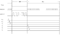
- one frame time (Vsync) is divided into a touch time period (Touch) and a display time period (Display), data signals and gate lines Gn-2, Gn-1, Gn, G3, G2, and G1. Only works during the display time period, and the touch signal works only during the touch time period. In this way, the duration of the touch time period and the display time period is relatively small in each frame.
- the insufficient time due to the time-division driving causes various display problems and touch problems.
- the embodiment of the invention provides an in-cell touch panel and a display device for overcoming various display problems and touch problems caused by insufficient time caused by the on-time driving touch and display functions of the in-cell touch screen.
- At least one embodiment of the present invention provides an in-cell touch panel including: an array substrate having a gate line and a common electrode layer, and a counter substrate opposite to the array substrate: the common electrode layer of the array substrate includes a plurality of sub-electrodes arranged in an array; wherein each sub-electrode spaced apart in each of the sub-electrodes serves as a touch driving sub-electrode to form a touch driving electrode, and a sub-electrode other than the touch driving sub-electrode As a common sub-electrode; when the gate lines covered by the row of sub-electrodes are scanned line by line, the row of sub-electrodes are used to load the common electrode signals, and the touch-driving sub-electrodes in the row-sub-electrodes other than the row of sub-electrodes For loading the touch drive signal, a common sub-electrode in the row sub-electrodes other than the row of
- the opposite substrate has a plurality of touch sensing electrodes that intersect with the touch driving electrodes, and an orthographic projection of each of the touch sensing electrodes on the array substrate is located at the common sub-electrode In the area.
- the array substrate is provided with a touch signal line corresponding to the touch driving electrode in one-to-one relationship, and a display control line and a touch corresponding to the sub-electrode row of the touch driving sub-electrode. Control lines, as well as common electrode signal lines.
- the touch driving sub-electrode is connected to the touch signal line corresponding to the touch control driving electrode through the touch switch device, and the control end of the touch switch device and the row sub-electrode are correspondingly touched.
- the touch control device is configured to conduct the touch signal line and the touch driving sub-electrode when the gate line covered by the row sub-electrodes except the row sub-electrode is progressively scanned; In each row of sub-electrodes, the touch driving sub-electrode is connected to the common electrode signal line through a display switching device, and the control end of the display switching device is connected to a display control line corresponding to the row of sub-electrodes; When the gate lines covered by the row of sub-electrodes are progressively scanned, the common electrode signal lines are electrically connected to the touch driving sub-electrodes.
- the touch switch device includes: a first switching transistor having a gate connected to the touch control line, a drain connected to the touch driving sub-electrode, and a source connected to the touch signal line;
- the display switching device includes: a second switching transistor having a gate connected to the display control line, a drain connected to the touch driving sub-electrode, and a source connected to the common electrode signal line.
- the first switching transistor and the second switching transistor are both N-type transistors or P-type transistors, and display control lines and touch control lines corresponding to the same row of sub-electrodes are used to load control signals of opposite polarities at the same time.
- the first switching transistor and the second switching transistor are an N-type transistor and a P-type transistor, respectively, and the display control line and the touch control line corresponding to the same row of sub-electrodes are used to load control signals of the same polarity at the same time.
- a display control line corresponding to each row of sub-electrodes is connected to a gate line covered by the row of sub-electrodes through a conduction device, and is connected to a last-scanned gate line covered by the row of sub-electrodes by a turn-off device, and the control terminal of the cut-off device is
- the row control electrodes are connected to the touch control lines; the conduction device and the cut-off device are configured to cause the display control lines to have control signals of opposite polarities when scanning the gate lines covered by the row of sub-electrodes and ending the scanning.
- the conduction device is a third switching transistor having a gate and a source connected to a corresponding gate line, and a drain connected to the display control line;
- the off device is a fourth switching transistor having a gate and a touch The control lines are connected, the source is connected to the gate line, and the drain is connected to the display control line.
- the common electrode layer is divided into a plurality of sub-electrodes arranged in an array, and the touch driving is performed.
- the sub-electrodes and the common sub-electrodes are arranged at intervals in the row direction and the column direction of the matrix.
- the touch driving sub-electrodes and the common sub-electrodes are arranged in a row in a matrix.
- a display device includes any of the above-mentioned in-cell touch panels provided by the embodiments of the present invention.
- 1 is a timing diagram of an in-cell touch screen
- FIG. 2 is a longitudinal cross-sectional view of an in-cell touch panel according to an embodiment of the present invention.
- 3a and 3b are top views of an in-cell touch panel according to an embodiment of the present invention.
- 4a is a schematic diagram of an array substrate in an in-cell touch panel according to an embodiment of the present invention.
- Figure 4b is a timing diagram of the operation of Figure 4a.
- 110-gate line 120-common electrode layer; 100-array substrate; 200-opposing substrate; 121-touch driving electrode; 210-touch sensing electrode; a-touch driving sub-electrode; b-common sub-electrode.
- FIG. 2 is a schematic longitudinal cross-sectional view of an in-cell touch panel according to an embodiment of the present invention.
- An in-cell touch panel provided by an embodiment of the present invention includes an array substrate 100 having a gate line 110 and a common electrode layer 120, and a counter substrate 200 disposed opposite the array substrate 100.
- the common electrode layer 120 is disposed above the gate line 110;
- the opposite substrate 200 is a color filter substrate, and includes a color filter unit corresponding to the sub-pixel unit on the array substrate 100, and may further include a black matrix or the like.
- the common electrode layer 120 of the array substrate 100 includes a plurality of sub-electrodes arranged in an array; in each column of sub-electrodes, the sub-electrodes provided at intervals are used as the touch driving sub-electrodes a, which constitute A touch driving electrode 121 (shown as a filled block in FIGS. 3a and 3b), a sub-electrode other than the touch driving sub-electrode a serves as a common sub-electrode b.
- the opposite substrate 200 has a plurality of touch sensing electrodes 210 intersecting with the touch driving electrodes 121.
- the orthographic projections of the touch sensing electrodes 210 on the array substrate 100 are located in the region where the common sub-electrode b is located; for example, as shown in FIG.
- each of the touch driving electrodes 121 disposed on the array substrate 100 extends in a longitudinal direction, and each of the touch sensing electrodes 210 disposed on the opposite substrate 200 extends laterally.
- a suitable mutual capacitance can be formed between the touch sensing electrode and the touch driving electrode to avoid a large mutual capacitance between the touch sensing electrode and the touch driving electrode. It is more conducive to the detection of touch positions.
- the sub-electrodes of the corresponding row are used to load the common electrode signal (Vcom), and the touch driving sub-electrodes in the row sub-electrodes other than the row of sub-electrodes For loading a touch driving signal (Touch), a common sub-electrode in other row sub-electrodes other than the row of sub-electrodes is used to load a common electrode signal (Vcom); that is, when a row of sub-electrodes are displayed, other touches are Control the drive sub-electrode for touch drive.
- Vcom common electrode signal
- the target of simultaneous display and touch operation can be achieved, and various displays caused by insufficient time due to time-division driving during high-resolution display can be ensured. Problems and touch issues.
- a plurality of sub-electrodes arranged in an array formed by the common electrode layer of the array substrate may be divided into a touch driving sub-electrode and a common sub-electrode in the following two manners. .
- the touch driving sub-electrode a and the common sub-electrode b are arranged in a row in a matrix, that is, one row of the touch driving sub-electrode a and one row of the common sub-electrode b are arranged at intervals.
- Figure 3a shows 8 touch drive electrodes Tx1...Tx8, each of the touch drive electrodes is composed of 8 touch drive sub-electrodes a, and the touch sensing electrodes intersecting with the touch drive electrodes 121 are also provided with 8 Rx1...Rx8.
- FIG. 3b shows eight touch driving electrodes Tx1...Tx8, each of which The strip touch driving electrodes are respectively composed of 8 touch driving sub-electrodes a.
- the following uses the array substrate in the first manner as an example to describe how the in-cell touch panel provided by the embodiment of the present invention realizes simultaneous display and touch driving.
- the common electrode layer of the array substrate includes 3*3 sub-electrodes, wherein the first row and the third row of sub-electrodes serve as touch driving sub-electrodes, and the second row of sub-electrodes serve as common sub-electrodes.
- the touch driving sub-electrode is divided into three longitudinally extending touch driving electrodes Tx1, Tx2, and Tx3, and each of the touch driving electrodes is composed of two touch driving sub-electrode segments 1 and 2.
- each touch driving sub-electrode is designed as a square electrode of about 5 mm*5 mm.
- the display density of the display is usually on the order of microns. Therefore, generally one touch driving sub-electrode corresponds to a plurality of pixel units in the display screen. That is, one touch drive sub-electrode covers a plurality of gate lines. In FIG.
- a row of sub-electrodes covering three gate lines is taken as an example, wherein the first row of sub-electrodes covers Gate n+1, Gate n+2, and Gate n+3 (ie, n+1 to n+). 3 gate lines), the second row of sub-electrodes covers Gate n+4, Gate n+5, and Gate n+6 (ie, n+4 to n+6 gate lines), and the third row of sub-electrodes covers Gate n +7, Gate n+8 and Gate n+9 (ie n+7 to n+9 grid lines).
- the gate drive circuit GOA connected to each gate line scans each gate line line by line. As shown in FIG. 4b, when scanning from the gate line Gate n+1 to Gate n+3, the first row of sub-electrodes Tx1, 1, Tx2, and Tx3, segment 1 are used as common sub-electrodes, and the common electrode is loaded.
- the signal Vcom, the touch driving sub-electrode Tx1 segment 2, the Tx2 segment 2 and the Tx3 segment 2 in the third row of sub-electrodes perform touch scanning, load the touch driving signal Touch; and so on, from the gate line Gate n
- the second row of sub-electrodes are used as common sub-electrodes, and the common electrode signal Vcom is loaded, and the touch driving sub-electrodes Tx1 in the first and third rows of sub-electrodes are segmented 1, Tx2 Segment 1, Tx3 segment 1, Tx1 segment 2, Tx2 segment 2, and Tx3 segment 2 perform touch scan, load touch drive signal Touch; scan from gate line Gate n+7 to Gate When n+9, the touch driving sub-electrodes Tx1 segment 2, Tx2 segment 2, and Tx3 segment 2 in the third row of sub-electrodes are used as common sub-electrodes, and the common electrode signal Vcom is
- the scanning frequency of the touch driving can be twice that of the display driving.
- the display driver can scan at 60 Hz, and the touch driving can reach 120 Hz, which can meet the requirements of general touch driving (80 Hz-120 Hz). .
- the following is an example of how the common electrode layer of the array substrate shown in FIG. 4a includes 3*3 sub-electrodes, and how to control the same touch driving sub-electrode loading in different time periods in the above-mentioned embedded touch screen provided by the embodiment of the present invention. Different electrical signals.
- the array substrate 100 is generally provided with touch signal lines T1, T2, and T3 corresponding to the touch driving electrodes Tx1, Tx2, and Tx3 in a non-display area, and a touch driving sub-electrode.
- the sub-electrode rows ie, the first row and the third row
- the non-display area of the array substrate extends in a longitudinal direction.
- the touch driving sub-electrode is connected to the touch signal line corresponding to the touch control driving electrode through the touch switch device, and the touch control corresponding to the control electrode of the touch switch device and the row sub-electrode Lines are connected.
- the touch driving sub-electrode Tx1 segment 1 is connected to the touch signal line T1 through the touch switch device M1a, and the control end of the touch switch device M1a is connected to A1; the touch switch device M1a is used to remove When the gate lines (Gate n+4 to Gate n+9) covered by the row sub-electrodes (the second row and the third row) other than the row sub-electrodes (the first row) are progressively scanned, the touch signal line T1 is touched.
- the segment 1 of the touch driving sub-electrode Tx1 is turned on to load the touch driving sub-electrode Tx1 into the touch scanning signal.
- the touch driving sub-electrode is connected to the common electrode signal line through the display switching device, and the control end of the display switching device is connected to the display control line corresponding to the row sub-electrode.
- the touch driving sub-electrode Tx1 segment 1 is connected to the common electrode signal line V through the display switching device N1a, and the control terminal of the display switching device N1a is connected to the display control line S1; the display switching device N1a is used for When the gate lines Gate n+1 to Gate n+3 covered by the row sub-electrodes (first row) are progressively scanned, the common electrode signal line V and the touch driving sub-electrode Tx1 are segmented 1 to The touch driving sub-electrode Tx1 segment 1 is loaded with the common electrode signal so that it can cooperate with the pixel electrode of the sub-pixel of the corresponding row to perform a display operation.
- the touch switch device M1a may include: a first switching transistor having a gate connected to the touch control line A1, a drain connected to the touch driving sub-electrode Tx1 segment 1, and a source and The touch signal line T1 is connected;
- the display switching device N1a may include: a second switching transistor having a gate connected to the display control line S1, a drain connected to the touch driving sub-electrode Tx1 segment 1, and a source and a common electrode signal.
- Line V is connected.
- the electric signals loaded on the touch control line and the display control line serve as control signals for turning on and off the switching transistors, respectively. Therefore, the corresponding control signal can be set according to the type of the switching transistor. For example, when both the first switching transistor and the second switching transistor are N-type transistors or P-type transistors, display control lines and touch control lines corresponding to the same row of sub-electrodes are applied to load control signals of opposite polarities at the same time. As shown in FIG.
- the control signals loaded by A1 and S1, A2, and S2 are shown to ensure that the first switching transistor and the second switching transistor are selectively turned on; when the first switching transistor and the second switching transistor are N-type transistors, respectively.
- the P-type transistor, the display control line and the touch control line corresponding to the same row of sub-electrodes are used to load the control signals of the same polarity at the same time to ensure that the first switching transistor and the second switching transistor are selectively turned on.
- the display control line corresponding to each row of sub-electrodes may be connected to the gate line covered by the row of sub-electrodes through the conduction device, and connected to the last scanned gate line covered by the row of sub-electrodes by the off-gate device, and the device is cut off.
- the control end is connected to the touch control line corresponding to the row of sub-electrodes.
- the display control line S1 corresponding to the first row of sub-electrodes is connected to the gate lines Gate n+1 to Gate n+3 through the three conduction devices O1a, respectively, and the last scanned gate line covered by the off device P1 and the row of sub-electrodes Gate n+3 is connected.
- the control terminal of the cutoff device P1 is connected to the touch control line A1 corresponding to the row of sub-electrodes.
- the turn-on device O1a and the turn-off device P1 are used to cause the display control lines to have control signals of opposite polarities when scanning the gate lines covered by the row of sub-electrodes and at the end of scanning. That is, the gate line Gate When n+1 to Gate n+3 is scanned, the signal loaded on the display control line S1 is the same as the signal loaded by the gate line, for example, a high level signal, and becomes a low level when the gate line Gate n+3 ends scanning. The signal, at this time, pulls the signal on the display control line S1 to a low level signal.
- the above-mentioned conduction device O1a is a third switching transistor whose gate and source are connected to the corresponding gate line Gate n+1, and the drain is connected to the display control line S1; the above-mentioned cut-off device P1 is the fourth The switching transistor has a gate connected to the touch control line A1, a source connected to the gate line Gate n+3, and a drain connected to the display control line S1.
- the embodiment of the present invention further provides a display device, which includes any of the above-mentioned embedded touch screens provided by the embodiments of the present invention, and the display device may be: a mobile phone, a watch, a tablet computer, a television, a display, a notebook computer, a digital photo frame, Any product or part that has a display function, such as a navigator.
- the display device reference may be made to the above embodiment of the in-cell touch panel, and the repeated description is omitted.
- An in-cell touch panel and a display device divide a common electrode layer connected to the entire surface of the array substrate to form a plurality of sub-electrodes arranged in an array, and each sub-electrode is arranged at intervals
- the electrode is used as a touch driving sub-electrode to form a touch driving electrode, and the sub-electrode other than the touch driving sub-electrode is used as a common sub-electrode; and a plurality of touch sensing electrodes are disposed on the opposite substrate and intersect with the touch driving electrode.
- the electrodes, the projections of the respective touch sensing electrodes on the array substrate are located in a region where the common sub-electrodes are located.
- the following driving method may be adopted: when the gate lines covered by the sub-electrodes of each row are progressively scanned, the row sub-electrodes are used to load the common electrode signals, and the touch drivers in the row sub-electrodes other than the row sub-electrodes
- the electrode is used to load the touch driving signal
- the common sub-electrode in the row sub-electrodes other than the row sub-electrode is used to load the common electrode signal; that is, when the row of sub-electrodes is displayed, the other rows of the touch driving sub-electrode Touch drive.
Landscapes
- Engineering & Computer Science (AREA)
- General Engineering & Computer Science (AREA)
- Theoretical Computer Science (AREA)
- Human Computer Interaction (AREA)
- Physics & Mathematics (AREA)
- General Physics & Mathematics (AREA)
- Computer Networks & Wireless Communication (AREA)
- Liquid Crystal (AREA)
- Devices For Indicating Variable Information By Combining Individual Elements (AREA)
- Position Input By Displaying (AREA)
- Control Of Indicators Other Than Cathode Ray Tubes (AREA)
- Liquid Crystal Display Device Control (AREA)
Abstract
一种内嵌式触摸屏及显示装置,将阵列基板(100)中的公共电极层(120)分割成多个呈阵列排布的子电极,将每列子电极中间隔设置的各子电极作为触控驱动子电极(a)组成一触控驱动电极(121),除此之外的子电极作为公共子电极(b);在对各行子电极覆盖的栅线(110)逐行扫描时,该行子电极加载公共电极信号,在其他行子电极中的触控驱动子电极(a)加载触控驱动信号,其他行子电极中的公共子电极(b)加载公共电极信号。该内嵌式触摸屏可以避免分时驱动导致的时间不足所引起的各种显示问题和触控问题。
Description
本发明的实施例涉及一种内嵌式触摸屏及显示装置。
通常,内嵌(In cell)式触摸屏是利用互电容的原理实现手指触摸位置的检测。一般在触摸屏中增加触控电极的图案。为了避免触控电极加载的触控信号和触摸屏中正常的显示信号之间相互干扰,一般采用分时驱动触控功能和显示功能。如图1所示,将一帧时间(Vsync)分为触控时间段(Touch)和显示时间段(Display),数据信号和栅线Gn-2、Gn-1、Gn、G3、G2和G1仅在显示时间段工作,触控信号仅在触控时间段工作。这样在每一帧中分配到触控时间段和显示时间段的时长相对较少,在需要高分辨率显示时,由于分时驱动导致的时间不足会引起各种显示问题和触控问题。
发明内容
本发明实施例提供一种内嵌式触摸屏及显示装置,用以克服内嵌式触摸屏需要分时驱动触控和显示功能导致的由于时间不足引起的各种显示问题和触控问题。
本发明至少一个实施例提供一种内嵌式触摸屏,包括:具有栅线和公共电极层的阵列基板,以及与所述阵列基板相对而置的对向基板:所述阵列基板的公共电极层包括多个呈阵列排布的子电极;其中,在每列所述子电极中间隔设置的各子电极作为触控驱动子电极组成一触控驱动电极,除触控驱动子电极之外的子电极作为公共子电极;在各行子电极覆盖的所述栅线逐行扫描时,该行子电极用于加载公共电极信号,在除该行子电极以外的其他行子电极中的触控驱动子电极用于加载触控驱动信号,在除该行子电极以外的其他行子电极中的公共子电极用于加载公共电极信号。
例如,所述对向基板具有多条与所述触控驱动电极交叉而置的触控感应电极,各所述触控感应电极在所述阵列基板上的正投影位于所述公共子电极
所在区域内。
例如,所述阵列基板在非显示区域设置有:与所述触控驱动电极一一对应的触控信号线,与具有触控驱动子电极的子电极行一一对应的显示控制线和触控控制线,以及公共电极信号线。
例如,各行子电极中,触控驱动子电极通过触控开关器件与所属的触控驱动电极对应的触控信号线相连,且所述触控开关器件的控制端与该行子电极对应的触控控制线相连;所述触控开关器件用于在除该行子电极以外的其他行子电极覆盖的所述栅线逐行扫描时,将触控信号线与触控驱动子电极导通;各行子电极中,触控驱动子电极通过显示开关器件与所述公共电极信号线相连,且所述显示开关器件的控制端与该行子电极对应的显示控制线相连;所述显示开关器件用于在该行子电极覆盖的所述栅线逐行扫描时,将公共电极信号线与触控驱动子电极导通。
例如,所述触控开关器件包括:第一开关晶体管,其栅极与所述触控控制线相连、漏极与所述触控驱动子电极相连、源极与所述触控信号线相连;例如,所述显示开关器件包括:第二开关晶体管,其栅极与所述显示控制线相连、漏极与所述触控驱动子电极相连、源极与所述公共电极信号线相连。
例如,所述第一开关晶体管和第二开关晶体管均为N型晶体管或P型晶体管,与同一行子电极对应的显示控制线和触控控制线用于在同一时刻加载相反极性的控制信号;所述第一开关晶体管和第二开关晶体管分别为N型晶体管和P型晶体管,与同一行子电极对应的显示控制线和触控控制线用于在同一时刻加载相同极性的控制信号。
例如,各行子电极对应的显示控制线通过导通器件与该行子电极覆盖的栅线相连,通过截止器件与该行子电极覆盖的最后扫描的栅线相连,所述截止器件的控制端与该行子电极对应的触控控制线相连;所述导通器件和截止器件用于在该行子电极覆盖的栅线进行扫描时和结束扫描时使显示控制线具有相反极性的控制信号。
例如,所述导通器件为第三开关晶体管,其栅极和源极与对应的栅线相连,漏极与显示控制线相连;所述截止器件为第四开关晶体管,其栅极与触控控制线相连,源极与栅线相连,漏极与显示控制线相连。
例如,所述公共电极层分割成的多个呈阵列排布的子电极中,触控驱动
子电极和公共子电极在矩阵的行方向和列方向均间隔排列。
例如,所述公共电极层分割成的多个呈阵列排布的子电极中,触控驱动子电极和公共子电极在矩阵中均整行排列。
本发明实施例提供的一种显示装置,包括本发明实施例提供的上述任一内嵌式触摸屏。
为了更清楚地说明本发明实施例的技术方案,下面将对实施例的附图作简单地介绍,显而易见地,下面描述中的附图仅仅涉及本发明的一些实施例,而非对本发明的限制。
图1为一种内嵌式触摸屏的时序图;
图2为本发明实施例提供的内嵌式触摸屏的纵向剖面示意图;
图3a和图3b分别为本发明实施例提供的内嵌式触摸屏的俯视图;
图4a为本发明实施例提供的内嵌式触摸屏中阵列基板的示意图;
图4b为图4a的工作时序图。
附图标记:
110-栅线;120-公共电极层;100-阵列基板;200-对向基板;121-触控驱动电极;210-触控感应电极;a-触控驱动子电极;b-公共子电极。
为了能够更清楚地理解本发明的上述目的、特征和优点,下面结合附图,对本发明实施例提供的内嵌式触摸屏及显示装置的具体实施方式进行详细地说明。显然,所描述的实施例是本发明的一部分实施例,而不是全部的实施例。基于所描述的本发明的实施例,本领域普通技术人员在无需创造性劳动的前提下所获得的所有其他实施例,都属于本发明保护的范围。
除非另作定义,此处使用的技术术语或者科学术语应当为本发明所属领域内具有一般技能的人士所理解的通常意义。本公开中使用的“第一”、“第二”以及类似的词语并不表示任何顺序、数量或者重要性,而只是用来区分不同的组成部分。附图中各层膜层的厚度和形状不反映真实比例,目的只是示意说明本发明实施例的内容。
图2为本发明实施例提供的内嵌式触摸屏的纵向剖面示意图。本发明实施例提供的一种内嵌式触摸屏,如图2所示,包括:具有栅线110和公共电极层120的阵列基板100,以及与阵列基板100相对而置的对向基板200。例如,该公共电极层120设置在栅线110上方;例如,对向基板200为彩膜基板,包括与阵列基板100上的子像素单元对应的滤色单元,还可以包括黑矩阵等。
如图3a和图3b所示,阵列基板100的公共电极层120包括多个呈阵列排布的子电极;在每列子电极中,间隔设置的各子电极作为触控驱动子电极a,它们组成一触控驱动电极121(图3a和图3b中带填充的方块所示),除触控驱动子电极a之外的子电极作为公共子电极b。
对向基板200具有多条与触控驱动电极121交叉而置的触控感应电极210,各触控感应电极210在阵列基板100上的正投影位于公共子电极b所在区域内;例如,如图3a所示,在阵列基板100上设置的各条触控驱动电极121均为纵向延伸,则在对向基板200上设置的各条触控感应电极210均为横向延伸。如此设置触控感应电极,可以在触控感应电极与触控驱动电极之间形成大小较为合适的互电容,避免触控感应电极与触控驱动电极之间形成较大的互电容,相对来说,更有利于触控位置的检测。
在各行子电极覆盖(对应)的栅线逐行扫描时,相应行的子电极用于加载公共电极信号(Vcom),在除该行子电极以外的其他行子电极中的触控驱动子电极用于加载触控驱动信号(Touch),在除该行子电极以外的其他行子电极中的公共子电极用于加载公共电极信号(Vcom);即在一行子电极进行显示时,其他行触控驱动子电极进行触控驱动。
通过采用本发明实施例提供的上述内嵌式触摸屏的驱动方式,可以达成显示和触控同时工作的目标,保证在高分辨率显示时不会由于分时驱动导致的时间不足引起的各种显示问题和触控问题。
例如,本发明实施例提供的上述内嵌式触摸屏中,阵列基板的公共电极层分割成的多个呈阵列排布的子电极可以采用以下两种方式划分为触控驱动子电极和公共子电极。
第一种,如图3a所示,触控驱动子电极a和公共子电极b在矩阵中均整行排列,即一行触控驱动子电极a和一行公共子电极b间隔排列。图3a示出
了8条触控驱动电极Tx1……Tx8,每条触控驱动电极分别由8个触控驱动子电极a组成,而与触控驱动电极121交叉而置的触控感应电极也设置了8条Rx1……Rx8。
第二种,如图3b所示,触控驱动子电极a和公共子电极b在矩阵的行方向和列方向均间隔排列,图3b示出了8条触控驱动电极Tx1……Tx8,每条触控驱动电极分别由8个触控驱动子电极a组成。
下面以采用第一种方式的阵列基板为例详细说明本发明实施例提供的上述内嵌式触摸屏是如何实现显示和触控驱动同时工作的。
以阵列基板的公共电极层包含3*3个子电极为例,如图4a所示,其中,第一行和第三行子电极均作为触控驱动子电极,第二行子电极作为公共子电极,将触控驱动子电极划分为3条纵向延伸的触控驱动电极Tx1、Tx2和Tx3,每条触控驱动电极分别由两个触控驱动子电极分段1和分段2组成。
一般地,触摸屏的触控密度通常在毫米级。因此,在具体实施时,可以根据所需的触控密度选择各触控驱动子电极的密度和所占面积,通常各触控驱动子电极设计为5mm*5mm左右的方形电极。显示屏的显示密度通常在微米级。因此,一般一个触控驱动子电极会对应显示屏中的多个像素单元。即一个触控驱动子电极会覆盖多条栅线。在图4a中以一行子电极覆盖3条栅线为例进行说明,其中,第一行子电极覆盖Gate n+1、Gate n+2和Gate n+3(即第n+1条到n+3条栅线),第二行子电极覆盖Gate n+4、Gate n+5和Gate n+6(即第n+4条到n+6条栅线),第三行子电极覆盖Gate n+7、Gate n+8和Gate n+9(即第n+7条到n+9条栅线)。
在一帧的显示时间段(Display)内,与各条栅线连接的栅极驱动电路GOA会逐行扫描各条栅线。如图4b所示,在从栅线Gate n+1扫描到Gate n+3时,第一行子电极Tx1分段1、Tx2分段1和Tx3分段1作为公共子电极使用,加载公共电极信号Vcom,第三行子电极中的触控驱动子电极Tx1分段2、Tx2分段2和Tx3分段2进行触控扫描,加载触控驱动信号Touch;以此类推,从栅线Gate n+4扫描到Gate n+6时,第二行子电极作为公共子电极使用,加载公共电极信号Vcom,第一行和第三行子电极中的触控驱动子电极Tx1分段1、Tx2分段1、Tx3分段1、Tx1分段2、Tx2分段2和Tx3分段2进行触控扫描,加载触控驱动信号Touch;从栅线Gate n+7扫描到Gate
n+9时,第三行子电极中的触控驱动子电极Tx1分段2、Tx2分段2和Tx3分段2作为公共子电极使用,加载公共电极信号Vcom,第一行子电极中的触控驱动子电极Tx1分段1、Tx2分段1和Tx3分段1进行触控扫描,加载触控驱动信号(Touch)。这样保证在一帧时间内,整个面板中的三行子电极按照显示驱动,进行扫描一次,且每行子电极按照触控驱动,各进行扫描两次。这样可以达到触控驱动的扫描频率为显示驱动的扫描频率的2倍,例如,显示驱动以60Hz进行扫描,触控驱动就可以达到120Hz,能够满足一般的触控驱动的要求(80Hz-120Hz)。
下面以图4a所示的阵列基板的公共电极层包含3*3个子电极为例,说明在本发明实施例提供的上述内嵌式触摸屏中是如何在不同时间段控制同一触控驱动子电极加载不同的电信号。
如图4a所示,阵列基板100在非显示区域一般会设置有:与触控驱动电极Tx1、Tx2和Tx3一一对应的触控信号线T1、T2和T3,与具有触控驱动子电极的子电极行(即第一行和第三行)一一对应的显示控制线S1、S2和触控控制线A1、A2,以及公共电极信号线V;为了方便加载对应的电信号,这些布线一般在阵列基板的非显示区域呈纵向延伸。
各行子电极中,触控驱动子电极通过触控开关器件与所属的触控驱动电极对应的触控信号线相连,且所述触控开关器件的控制端与该行子电极对应的触控控制线相连。例如第一行中触控驱动子电极Tx1分段1通过触控开关器件M1a与触控信号线T1相连,且触控开关器件M1a的控制端与A1相连;触控开关器件M1a用于在除该行子电极(第一行)以外的其他行子电极(第二行和第三行)覆盖的栅线(Gate n+4至Gate n+9)逐行扫描时,将触控信号线T1与触控驱动子电极Tx1分段1导通,以便使触控驱动子电极Tx1分段1加载触控扫描信号。
各行子电极中,触控驱动子电极通过显示开关器件与公共电极信号线相连,且显示开关器件的控制端与该行子电极对应的显示控制线相连。例如,第一行中触控驱动子电极Tx1分段1通过显示开关器件N1a与公共电极信号线V相连,且显示开关器件N1a的控制端与显示控制线S1相连;显示开关器件N1a用于在该行子电极(第一行)覆盖的栅线Gate n+1至Gate n+3逐行扫描时,将公共电极信号线V与触控驱动子电极Tx1分段1导通,以
便使触控驱动子电极Tx1分段1加载公共电极信号,从而可以与相应行的亚像素的像素电极配合以进行显示操作。
以上仅以一个触控驱动子电极Tx1分段1为例进行说明,其他触控驱动子电极的工作原理以此类推,在此不作详述。
例如,如图4a所示,上述触控开关器件M1a可以包括:第一开关晶体管,其栅极与触控控制线A1相连、漏极与触控驱动子电极Tx1分段1相连、源极与触控信号线T1相连;上述显示开关器件N1a可以包括:第二开关晶体管,其栅极与显示控制线S1相连、漏极与触控驱动子电极Tx1分段1相连、源极与公共电极信号线V相连。
例如采用开关晶体管作为触控开关器件和显示开关器件时,触控控制线和显示控制线上加载的电信号分别作为导通和截止开关晶体管的控制信号。因此,可根据开关晶体管的类型设置对应控制信号。例如,在第一开关晶体管和第二开关晶体管均为N型晶体管或P型晶体管时,与同一行子电极对应的显示控制线和触控控制线应用于在同一时刻加载相反极性的控制信号,如图4b中A1和S1、A2和S2加载的控制信号所示,以保证第一开关晶体管和第二开关晶体管择一导通;当第一开关晶体管和第二开关晶体管分别为N型晶体管和P型晶体管,与同一行子电极对应的显示控制线和触控控制线用于在同一时刻加载相同极性的控制信号,以保证第一开关晶体管和第二开关晶体管择一导通。
进一步地,由于在阵列基板的非显示区域设置的走线数量较多,若对每一走线均单独设置输入信号,占用空间将非常大。因此,为了减少走线的占用空间,例如,可以利用其它走线上加载的信号来控制显示控制线S1和S2上加载的信号。如图4a所示,可以将各行子电极对应的显示控制线通过导通器件与该行子电极覆盖的栅线相连,通过截止器件与该行子电极覆盖的最后扫描的栅线相连,截止器件的控制端与该行子电极对应的触控控制线相连。例如第一行子电极对应的显示控制线S1通过三个导通器件O1a分别与栅线Gate n+1至Gate n+3相连,通过截止器件P1与该行子电极覆盖的最后扫描的栅线Gate n+3相连。截止器件P1的控制端与该行子电极对应的触控控制线A1相连。导通器件O1a和截止器件P1用于在该行子电极覆盖的栅线进行扫描时和结束扫描时使显示控制线具有相反极性的控制信号。即在栅线Gate
n+1至Gate n+3进行扫描时,显示控制线S1上加载的信号与栅线加载的信号相同,例如为高电平信号,当栅线Gate n+3扫描结束时变为低电平信号,此时将显示控制线S1上的信号拉为低电平信号。
如图4a所示,上述导通器件O1a为第三开关晶体管,其栅极和源极与对应的栅线Gate n+1相连,漏极与显示控制线S1相连;上述截止器件P1为第四开关晶体管,其栅极与触控控制线A1相连,源极与栅线Gate n+3相连,漏极与显示控制线S1相连。
本发明实施例还提供一种显示装置,包括本发明实施例提供的上述任一内嵌式触摸屏,该显示装置可以为:手机、手表、平板电脑、电视机、显示器、笔记本电脑、数码相框、导航仪等任何具有显示功能的产品或部件。该显示装置的实施可以参见上述内嵌式触摸屏的实施例,重复之处不再赘述。
本发明实施例提供的一种内嵌式触摸屏及显示装置,将阵列基板中整面连接的公共电极层进行分割形成多个呈阵列排布的子电极,将每列子电极中间隔设置的各子电极作为触控驱动子电极组成一触控驱动电极,除触控驱动子电极之外的子电极作为公共子电极;在对向基板上设置多条与触控驱动电极交叉而置的触控感应电极,各触控感应电极在阵列基板上的投影位于公共子电极所在的区域内。例如,可以采用以下驱动方式:在各行子电极覆盖的栅线逐行扫描时,该行子电极用于加载公共电极信号,在除该行子电极以外的其他行子电极中的触控驱动子电极用于加载触控驱动信号,在除该行子电极以外的其他行子电极中的公共子电极用于加载公共电极信号;即在一行子电极进行显示时,其他行的触控驱动子电极进行触控驱动。通过上述驱动方式,可以达成显示和触控同时工作的目标,保证在高分辨率显示时不会由于分时驱动导致的时间不足引起的各种显示问题和触控问题。
显然,本领域的技术人员可以对本发明进行各种改动和变型而不脱离本发明的精神和范围。这样,倘若本发明的这些修改和变型属于本发明权利要求及其等同技术的范围之内,则本发明也意图包含这些改动和变型在内。
本专利申请要求于2014年11月6日递交的中国专利申请第201410638383.5号的优先权,在此全文引用上述中国专利申请公开的内容以作为本申请的一部分。
Claims (12)
- 一种内嵌式触摸屏,包括:具有栅线和公共电极层的阵列基板,以及与所述阵列基板相对而置的对向基板,其中,所述阵列基板的公共电极层包括多个呈阵列排布的子电极;其中,在每列所述子电极中间隔设置的各子电极作为触控驱动子电极组成一触控驱动电极,除触控驱动子电极之外的子电极作为公共子电极;在各行子电极覆盖的所述栅线逐行扫描时,该行子电极用于加载公共电极信号,在除该行子电极以外的其他行子电极中的触控驱动子电极用于加载触控驱动信号,在除该行子电极以外的其他行子电极中的公共子电极用于加载公共电极信号。
- 如权利要求1所述的内嵌式触摸屏,其中,所述对向基板具有多条与所述触控驱动电极交叉而置的触控感应电极,各所述触控感应电极在所述阵列基板上的正投影位于所述公共子电极所在区域内。
- 如权利要求1所述的内嵌式触摸屏,其中,所述阵列基板在非显示区域设置有:与所述触控驱动电极一一对应的触控信号线,与具有触控驱动子电极的子电极行一一对应的显示控制线和触控控制线,以及公共电极信号线。
- 如权利要求3所述的内嵌式触摸屏,其中,各行子电极中,触控驱动子电极通过触控开关器件与所属的触控驱动电极对应的触控信号线相连,且所述触控开关器件的控制端与该行子电极对应的触控控制线相连;所述触控开关器件用于在除该行子电极以外的其他行子电极覆盖的所述栅线逐行扫描时,将触控信号线与触控驱动子电极导通;各行子电极中,触控驱动子电极通过显示开关器件与所述公共电极信号线相连,且所述显示开关器件的控制端与该行子电极对应的显示控制线相连;所述显示开关器件用于在该行子电极覆盖的所述栅线逐行扫描时,将公共电极信号线与触控驱动子电极导通。
- 如权利要求4所述的内嵌式触摸屏,其中,所述触控开关器件包括:第一开关晶体管,其栅极与所述触控控制线相连、漏极与所述触控驱动子电极相连、源极与所述触控信号线相连。
- 如权利要求5所述的内嵌式触摸屏,其中,所述显示开关器件包括:第二开关晶体管,其栅极与所述显示控制线相连、漏极与所述触控驱动子电极相连、源极与所述公共电极信号线相连。
- 如权利要求6所述的内嵌式触摸屏,其中,所述第一开关晶体管和第二开关晶体管均为N型晶体管或P型晶体管,与同一行子电极对应的显示控制线和触控控制线用于在同一时刻加载相反极性的控制信号;所述第一开关晶体管和第二开关晶体管分别为N型晶体管和P型晶体管,与同一行子电极对应的显示控制线和触控控制线用于在同一时刻加载相同极性的控制信号。
- 如权利要求3所述的内嵌式触摸屏,其中,各行子电极对应的显示控制线通过导通器件与该行子电极覆盖的栅线相连,通过截止器件与该行子电极覆盖的最后扫描的栅线相连,所述截止器件的控制端与该行子电极对应的触控控制线相连;所述导通器件和截止器件用于在该行子电极覆盖的栅线进行扫描时和结束扫描时使显示控制线具有相反极性的控制信号。
- 如权利要求8所述的内嵌式触摸屏,其中,所述导通器件为第三开关晶体管,其栅极和源极与对应的栅线相连,漏极与显示控制线相连;所述截止器件为第四开关晶体管,其栅极与触控控制线相连,源极与栅线相连,漏极与显示控制线相连。
- 如权利要求1-9任一项所述的内嵌式触摸屏,其中,所述公共电极层分割成的多个呈阵列排布的子电极中,触控驱动子电极和公共子电极在矩阵的行方向和列方向均间隔排列。
- 如权利要求1-9任一项所述的内嵌式触摸屏,其中,所述公共电极层分割成的多个呈阵列排布的子电极中,触控驱动子电极和公共子电极在矩阵中均整行排列。
- 一种显示装置,包括如权利要求1-11任一项所述的内嵌式触摸屏。
Priority Applications (2)
| Application Number | Priority Date | Filing Date | Title |
|---|---|---|---|
| EP15778596.5A EP3217264B1 (en) | 2014-11-06 | 2015-02-13 | In-cell touch screen and display device |
| US14/888,145 US9733743B2 (en) | 2014-11-06 | 2015-02-13 | In-cell touch screen and display device |
Applications Claiming Priority (2)
| Application Number | Priority Date | Filing Date | Title |
|---|---|---|---|
| CN201410638383.5A CN104391600B (zh) | 2014-11-06 | 2014-11-06 | 一种内嵌式触摸屏及显示装置 |
| CN201410638383.5 | 2014-11-06 |
Publications (1)
| Publication Number | Publication Date |
|---|---|
| WO2016070528A1 true WO2016070528A1 (zh) | 2016-05-12 |
Family
ID=52609512
Family Applications (1)
| Application Number | Title | Priority Date | Filing Date |
|---|---|---|---|
| PCT/CN2015/073009 Ceased WO2016070528A1 (zh) | 2014-11-06 | 2015-02-13 | 内嵌式触摸屏及显示装置 |
Country Status (4)
| Country | Link |
|---|---|
| US (1) | US9733743B2 (zh) |
| EP (1) | EP3217264B1 (zh) |
| CN (1) | CN104391600B (zh) |
| WO (1) | WO2016070528A1 (zh) |
Families Citing this family (9)
| Publication number | Priority date | Publication date | Assignee | Title |
|---|---|---|---|---|
| CN104699307B (zh) * | 2015-03-31 | 2017-10-17 | 京东方科技集团股份有限公司 | 一种触控显示驱动方法、驱动装置及触控显示器 |
| CN104699315B (zh) | 2015-04-01 | 2018-03-13 | 上海天马微电子有限公司 | 一种触控面板、触控显示面板和显示装置 |
| CN104699352B (zh) * | 2015-04-01 | 2018-04-13 | 上海天马微电子有限公司 | 一种自容式触控显示面板及其阵列基板 |
| CN104765506B (zh) | 2015-05-05 | 2019-01-08 | 京东方科技集团股份有限公司 | 触控显示面板及其驱动方法和触控显示装置 |
| TWI552030B (zh) * | 2015-07-24 | 2016-10-01 | 義隆電子股份有限公司 | 在觸控裝置上偵測主動式觸控筆的方法及該觸控裝置 |
| CN105572936A (zh) * | 2015-12-22 | 2016-05-11 | 武汉华星光电技术有限公司 | 窄边框In Cell型触控显示面板结构 |
| CN105760013B (zh) * | 2016-01-29 | 2019-06-07 | 厦门天马微电子有限公司 | 触控面板及触控显示装置 |
| CN105843454B (zh) * | 2016-06-01 | 2019-08-02 | 京东方科技集团股份有限公司 | 阵列基板、显示装置、驱动电路及驱动方法 |
| CN112735335B (zh) * | 2020-11-30 | 2022-04-29 | 武汉天马微电子有限公司 | 一种有机发光显示面板、显示装置及驱动方法 |
Citations (6)
| Publication number | Priority date | Publication date | Assignee | Title |
|---|---|---|---|---|
| CN103838431A (zh) * | 2014-02-24 | 2014-06-04 | 北京京东方光电科技有限公司 | 一种内嵌式触摸屏及显示装置 |
| CN103838430A (zh) * | 2014-02-24 | 2014-06-04 | 北京京东方光电科技有限公司 | 一种内嵌式触摸屏及显示装置 |
| KR20140087483A (ko) * | 2012-12-31 | 2014-07-09 | 엘지디스플레이 주식회사 | 터치스크린 일체형 표시장치 및 그 제조 방법 |
| CN204129705U (zh) * | 2014-11-06 | 2015-01-28 | 京东方科技集团股份有限公司 | 一种内嵌式触摸屏及显示装置 |
| CN104317467A (zh) * | 2014-11-06 | 2015-01-28 | 京东方科技集团股份有限公司 | 一种内嵌式触摸屏及显示装置 |
| CN204166510U (zh) * | 2014-11-06 | 2015-02-18 | 京东方科技集团股份有限公司 | 一种内嵌式触摸屏及显示装置 |
Family Cites Families (13)
| Publication number | Priority date | Publication date | Assignee | Title |
|---|---|---|---|---|
| TWI387801B (zh) | 2008-07-01 | 2013-03-01 | Chunghwa Picture Tubes Ltd | 移位暫存裝置及其方法 |
| US8217913B2 (en) * | 2009-02-02 | 2012-07-10 | Apple Inc. | Integrated touch screen |
| EP2447950A1 (en) | 2009-06-25 | 2012-05-02 | Sharp Kabushiki Kaisha | Shift register circuit, display device provided with same, and shift register circuit driving method |
| KR101330320B1 (ko) * | 2012-02-20 | 2013-11-14 | 엘지디스플레이 주식회사 | 터치스크린 일체형 표시장치 및 그 구동 방법 |
| KR101480315B1 (ko) * | 2012-08-16 | 2015-01-08 | 엘지디스플레이 주식회사 | 터치스크린 일체형 표시장치 및 그 구동 방법 |
| KR101480314B1 (ko) * | 2012-08-16 | 2015-01-08 | 엘지디스플레이 주식회사 | 터치스크린 일체형 표시장치 및 그 구동 방법 |
| TWI471782B (zh) * | 2012-11-14 | 2015-02-01 | Orise Technology Co Ltd | 內嵌式多點觸控液晶顯示面板系統 |
| CN102983132B (zh) | 2012-11-29 | 2015-04-22 | 京东方科技集团股份有限公司 | 阵列基板和显示装置 |
| KR101998769B1 (ko) | 2012-11-30 | 2019-07-10 | 엘지디스플레이 주식회사 | 협 베젤 영역을 갖는 평판 표시 패널 |
| CN103226412A (zh) * | 2013-04-10 | 2013-07-31 | 北京京东方光电科技有限公司 | 一种内嵌式触摸屏及显示装置 |
| CN104021769B (zh) | 2014-05-30 | 2016-06-15 | 京东方科技集团股份有限公司 | 一种移位寄存器、栅线集成驱动电路及显示屏 |
| CN104183225B (zh) | 2014-08-15 | 2017-08-15 | 上海天马微电子有限公司 | 一种驱动装置、阵列基板和显示装置 |
| CN104485085B (zh) | 2015-01-04 | 2017-07-21 | 京东方科技集团股份有限公司 | 一种阵列基板及显示装置 |
-
2014
- 2014-11-06 CN CN201410638383.5A patent/CN104391600B/zh active Active
-
2015
- 2015-02-13 WO PCT/CN2015/073009 patent/WO2016070528A1/zh not_active Ceased
- 2015-02-13 US US14/888,145 patent/US9733743B2/en not_active Expired - Fee Related
- 2015-02-13 EP EP15778596.5A patent/EP3217264B1/en active Active
Patent Citations (6)
| Publication number | Priority date | Publication date | Assignee | Title |
|---|---|---|---|---|
| KR20140087483A (ko) * | 2012-12-31 | 2014-07-09 | 엘지디스플레이 주식회사 | 터치스크린 일체형 표시장치 및 그 제조 방법 |
| CN103838431A (zh) * | 2014-02-24 | 2014-06-04 | 北京京东方光电科技有限公司 | 一种内嵌式触摸屏及显示装置 |
| CN103838430A (zh) * | 2014-02-24 | 2014-06-04 | 北京京东方光电科技有限公司 | 一种内嵌式触摸屏及显示装置 |
| CN204129705U (zh) * | 2014-11-06 | 2015-01-28 | 京东方科技集团股份有限公司 | 一种内嵌式触摸屏及显示装置 |
| CN104317467A (zh) * | 2014-11-06 | 2015-01-28 | 京东方科技集团股份有限公司 | 一种内嵌式触摸屏及显示装置 |
| CN204166510U (zh) * | 2014-11-06 | 2015-02-18 | 京东方科技集团股份有限公司 | 一种内嵌式触摸屏及显示装置 |
Also Published As
| Publication number | Publication date |
|---|---|
| EP3217264B1 (en) | 2021-04-28 |
| US9733743B2 (en) | 2017-08-15 |
| EP3217264A4 (en) | 2018-04-25 |
| CN104391600B (zh) | 2017-11-10 |
| CN104391600A (zh) | 2015-03-04 |
| US20160328059A1 (en) | 2016-11-10 |
| EP3217264A1 (en) | 2017-09-13 |
Similar Documents
| Publication | Publication Date | Title |
|---|---|---|
| EP2869166B1 (en) | Touch panel, touch display panel, and touch detection and display method | |
| US9851832B2 (en) | Display panel, driving method thereof and display device | |
| US10564745B2 (en) | Array substrate and display panel | |
| CN104317467B (zh) | 一种内嵌式触摸屏及显示装置 | |
| JP6518576B2 (ja) | 表示装置及び表示装置のタッチ検出方法 | |
| US10241606B2 (en) | Display device | |
| CN104407760B (zh) | 一种内嵌式触摸屏及显示装置 | |
| EP3217264B1 (en) | In-cell touch screen and display device | |
| JP6103394B2 (ja) | 入力装置、および液晶表示装置 | |
| EP3316237B1 (en) | Embedded touch control display screen and drive method therefor, and display device | |
| CN105182582B (zh) | 一种内嵌式触摸屏及显示装置 | |
| JP5807191B2 (ja) | 表示装置 | |
| WO2015117288A1 (zh) | 内嵌式触摸屏及显示装置 | |
| KR20150011583A (ko) | 표시장치 | |
| WO2014169538A1 (zh) | 内嵌式触摸屏及显示装置 | |
| CN103744239A (zh) | 一种内嵌式触控阵列基板结构 | |
| CN104866158A (zh) | 一种内嵌式触摸屏及显示装置 | |
| KR20130065564A (ko) | 터치 스크린 일체형 표시장치 | |
| JPWO2014045604A1 (ja) | 表示装置 | |
| CN204129705U (zh) | 一种内嵌式触摸屏及显示装置 | |
| JPWO2014045600A1 (ja) | 液晶表示装置 | |
| CN204166510U (zh) | 一种内嵌式触摸屏及显示装置 | |
| JP2020095491A (ja) | 表示装置 | |
| JPWO2014045603A1 (ja) | 入力装置 |
Legal Events
| Date | Code | Title | Description |
|---|---|---|---|
| REEP | Request for entry into the european phase |
Ref document number: 2015778596 Country of ref document: EP |
|
| WWE | Wipo information: entry into national phase |
Ref document number: 2015778596 Country of ref document: EP |
|
| WWE | Wipo information: entry into national phase |
Ref document number: 14888145 Country of ref document: US |
|
| 121 | Ep: the epo has been informed by wipo that ep was designated in this application |
Ref document number: 15778596 Country of ref document: EP Kind code of ref document: A1 |
|
| NENP | Non-entry into the national phase |
Ref country code: DE |