WO2016072213A1 - 変圧装置 - Google Patents
変圧装置 Download PDFInfo
- Publication number
- WO2016072213A1 WO2016072213A1 PCT/JP2015/078736 JP2015078736W WO2016072213A1 WO 2016072213 A1 WO2016072213 A1 WO 2016072213A1 JP 2015078736 W JP2015078736 W JP 2015078736W WO 2016072213 A1 WO2016072213 A1 WO 2016072213A1
- Authority
- WO
- WIPO (PCT)
- Prior art keywords
- circuit
- switch
- dead time
- nodes
- transformer
- Prior art date
- Legal status (The legal status is an assumption and is not a legal conclusion. Google has not performed a legal analysis and makes no representation as to the accuracy of the status listed.)
- Ceased
Links
Images



















Classifications
-
- H—ELECTRICITY
- H02—GENERATION; CONVERSION OR DISTRIBUTION OF ELECTRIC POWER
- H02M—APPARATUS FOR CONVERSION BETWEEN AC AND AC, BETWEEN AC AND DC, OR BETWEEN DC AND DC, AND FOR USE WITH MAINS OR SIMILAR POWER SUPPLY SYSTEMS; CONVERSION OF DC OR AC INPUT POWER INTO SURGE OUTPUT POWER; CONTROL OR REGULATION THEREOF
- H02M3/00—Conversion of DC power input into DC power output
- H02M3/02—Conversion of DC power input into DC power output without intermediate conversion into AC
- H02M3/04—Conversion of DC power input into DC power output without intermediate conversion into AC by static converters
- H02M3/10—Conversion of DC power input into DC power output without intermediate conversion into AC by static converters using discharge tubes with control electrode or semiconductor devices with control electrode
- H02M3/145—Conversion of DC power input into DC power output without intermediate conversion into AC by static converters using discharge tubes with control electrode or semiconductor devices with control electrode using devices of a triode or transistor type requiring continuous application of a control signal
- H02M3/155—Conversion of DC power input into DC power output without intermediate conversion into AC by static converters using discharge tubes with control electrode or semiconductor devices with control electrode using devices of a triode or transistor type requiring continuous application of a control signal using semiconductor devices only
- H02M3/156—Conversion of DC power input into DC power output without intermediate conversion into AC by static converters using discharge tubes with control electrode or semiconductor devices with control electrode using devices of a triode or transistor type requiring continuous application of a control signal using semiconductor devices only with automatic control of output voltage or current, e.g. switching regulators
- H02M3/158—Conversion of DC power input into DC power output without intermediate conversion into AC by static converters using discharge tubes with control electrode or semiconductor devices with control electrode using devices of a triode or transistor type requiring continuous application of a control signal using semiconductor devices only with automatic control of output voltage or current, e.g. switching regulators including plural semiconductor devices as final control devices for a single load
-
- H—ELECTRICITY
- H02—GENERATION; CONVERSION OR DISTRIBUTION OF ELECTRIC POWER
- H02M—APPARATUS FOR CONVERSION BETWEEN AC AND AC, BETWEEN AC AND DC, OR BETWEEN DC AND DC, AND FOR USE WITH MAINS OR SIMILAR POWER SUPPLY SYSTEMS; CONVERSION OF DC OR AC INPUT POWER INTO SURGE OUTPUT POWER; CONTROL OR REGULATION THEREOF
- H02M5/00—Conversion of AC power input into AC power output, e.g. for change of voltage, for change of frequency, for change of number of phases
- H02M5/02—Conversion of AC power input into AC power output, e.g. for change of voltage, for change of frequency, for change of number of phases without intermediate conversion into DC
- H02M5/04—Conversion of AC power input into AC power output, e.g. for change of voltage, for change of frequency, for change of number of phases without intermediate conversion into DC by static converters
- H02M5/10—Conversion of AC power input into AC power output, e.g. for change of voltage, for change of frequency, for change of number of phases without intermediate conversion into DC by static converters using transformers
- H02M5/12—Conversion of AC power input into AC power output, e.g. for change of voltage, for change of frequency, for change of number of phases without intermediate conversion into DC by static converters using transformers for conversion of voltage or current amplitude only
-
- H—ELECTRICITY
- H02—GENERATION; CONVERSION OR DISTRIBUTION OF ELECTRIC POWER
- H02M—APPARATUS FOR CONVERSION BETWEEN AC AND AC, BETWEEN AC AND DC, OR BETWEEN DC AND DC, AND FOR USE WITH MAINS OR SIMILAR POWER SUPPLY SYSTEMS; CONVERSION OF DC OR AC INPUT POWER INTO SURGE OUTPUT POWER; CONTROL OR REGULATION THEREOF
- H02M5/00—Conversion of AC power input into AC power output, e.g. for change of voltage, for change of frequency, for change of number of phases
- H02M5/02—Conversion of AC power input into AC power output, e.g. for change of voltage, for change of frequency, for change of number of phases without intermediate conversion into DC
- H02M5/04—Conversion of AC power input into AC power output, e.g. for change of voltage, for change of frequency, for change of number of phases without intermediate conversion into DC by static converters
- H02M5/22—Conversion of AC power input into AC power output, e.g. for change of voltage, for change of frequency, for change of number of phases without intermediate conversion into DC by static converters using discharge tubes with control electrode or semiconductor devices with control electrode
-
- H—ELECTRICITY
- H02—GENERATION; CONVERSION OR DISTRIBUTION OF ELECTRIC POWER
- H02M—APPARATUS FOR CONVERSION BETWEEN AC AND AC, BETWEEN AC AND DC, OR BETWEEN DC AND DC, AND FOR USE WITH MAINS OR SIMILAR POWER SUPPLY SYSTEMS; CONVERSION OF DC OR AC INPUT POWER INTO SURGE OUTPUT POWER; CONTROL OR REGULATION THEREOF
- H02M3/00—Conversion of DC power input into DC power output
- H02M3/02—Conversion of DC power input into DC power output without intermediate conversion into AC
- H02M3/04—Conversion of DC power input into DC power output without intermediate conversion into AC by static converters
- H02M3/10—Conversion of DC power input into DC power output without intermediate conversion into AC by static converters using discharge tubes with control electrode or semiconductor devices with control electrode
- H02M3/145—Conversion of DC power input into DC power output without intermediate conversion into AC by static converters using discharge tubes with control electrode or semiconductor devices with control electrode using devices of a triode or transistor type requiring continuous application of a control signal
- H02M3/155—Conversion of DC power input into DC power output without intermediate conversion into AC by static converters using discharge tubes with control electrode or semiconductor devices with control electrode using devices of a triode or transistor type requiring continuous application of a control signal using semiconductor devices only
-
- H—ELECTRICITY
- H02—GENERATION; CONVERSION OR DISTRIBUTION OF ELECTRIC POWER
- H02M—APPARATUS FOR CONVERSION BETWEEN AC AND AC, BETWEEN AC AND DC, OR BETWEEN DC AND DC, AND FOR USE WITH MAINS OR SIMILAR POWER SUPPLY SYSTEMS; CONVERSION OF DC OR AC INPUT POWER INTO SURGE OUTPUT POWER; CONTROL OR REGULATION THEREOF
- H02M5/00—Conversion of AC power input into AC power output, e.g. for change of voltage, for change of frequency, for change of number of phases
- H02M5/02—Conversion of AC power input into AC power output, e.g. for change of voltage, for change of frequency, for change of number of phases without intermediate conversion into DC
- H02M5/04—Conversion of AC power input into AC power output, e.g. for change of voltage, for change of frequency, for change of number of phases without intermediate conversion into DC by static converters
- H02M5/22—Conversion of AC power input into AC power output, e.g. for change of voltage, for change of frequency, for change of number of phases without intermediate conversion into DC by static converters using discharge tubes with control electrode or semiconductor devices with control electrode
- H02M5/275—Conversion of AC power input into AC power output, e.g. for change of voltage, for change of frequency, for change of number of phases without intermediate conversion into DC by static converters using discharge tubes with control electrode or semiconductor devices with control electrode using devices of a triode or transistor type requiring continuous application of a control signal
- H02M5/293—Conversion of AC power input into AC power output, e.g. for change of voltage, for change of frequency, for change of number of phases without intermediate conversion into DC by static converters using discharge tubes with control electrode or semiconductor devices with control electrode using devices of a triode or transistor type requiring continuous application of a control signal using semiconductor devices only
Definitions
- the present invention relates to a transformer device.
- Transformers are used for commercial AC transmission and distribution systems. Near the customer, for example, a pole transformer that transforms 6600 V (50 Hz or 60 Hz) to 200 V is used (see Non-Patent Document 1). In such a transformer on a pole, a thick coil serving as a conducting wire is wound around an iron core and has a corresponding weight. Further, if insulating oil and a case are further included, for example, a type having a diameter of 40 cm and a height of 80 cm has a weight of about 200 kg.
- SST Solid-State Transformer
- a high-frequency transformer is used for SST (see, for example, Non-Patent Document 2).
- the output voltage of solar power generation may be as high as 1000V, and in order to step down the voltage to about 100 to 200V, a device such as a step-down transformer is required on the way, like an AC circuit.
- the present invention provides a revolutionary next-generation transformer that is small and light and does not require magnetic coupling, electromagnetic induction, a coil for mutual inductance, an iron core, or the like as in a conventional transformer.
- the purpose is to provide.
- the power source may be either AC or DC.
- the transformer device of the present invention is provided between a power source and a load, and is constituted by a front-stage circuit and a rear-stage circuit.
- a plurality of switches that are multiples of 2 are connected in series with each other, and odd-numbered switches and even-numbered switches viewed alternately from one end side of the series body
- a switch series body that is turned on and connected in parallel to the power supply as a whole; and
- the switch series body with the interconnection points of the switches and both end points of the switch series body as a total of m nodes.
- a capacitor provided on at least one electric circuit and corresponding to at least (m ⁇ 1) nodes, and (c) a pair of semiconductor elements that perform current-carrying operations of opposite polarities as the subsequent circuit.
- the transformer device of the present invention it is possible to provide a revolutionary next-generation transformer device that is small and light and does not require magnetic coupling, electromagnetic induction, a coil for mutual inductance, an iron core, or the like as in a conventional transformer. Can do.
- FIG. 1 It is a circuit diagram of a transformer as a basic form of a transformer according to the present embodiment.
- (A) is a circuit diagram showing a state of substantial connection when two switches on the upper side of the four switches in FIG. 1 are on and two switches on the lower side are off
- (B) is a circuit diagram in which the same circuit diagram as (a) is rewritten stepwise.
- (A) is a circuit diagram showing a state of substantial connection when two switches on the lower side among the four switches in FIG. 1 are on and two switches on the upper side are off
- (B) is a circuit diagram in which the same circuit diagram as (a) is rewritten stepwise.
- the upper diagram is a waveform diagram showing the input voltage to the transformer, and the lower diagram is the input current.
- Voltage v m at the intermediate stage of the transformer, the current i m is a waveform diagram illustrating respectively.
- the upper diagram is a waveform diagram showing the output voltage from the transformer, and the lower diagram is the output current.
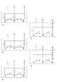
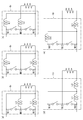
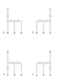
- It is a circuit diagram which shows an example of the transformer apparatus developed more practically. It is a circuit diagram which shows the variation of topology about the principal part of a front
- FIG. 11 is a diagram showing another circuit variation of the first electric circuit when the total number of capacitors is not reduced from the first electric circuit (solid line) in FIG. 10.
- FIG. 11 is a diagram showing a circuit variation of the first electric circuit when the total number of capacitors is reduced by one from the first electric circuit (solid line) in FIG. 10.
- FIG. 8 is a circuit diagram in which the diodes and the bleeder resistors in FIG.
- FIG. 21 is a background diagram similar to FIG. 20, but also shows a current path in the second half time ⁇ 2 . It is a graph which shows an example of the current waveform which flows into an inductor.
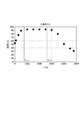
- FIG. 23 is an enlarged view near the top of the waveform of FIG. 22. It is the figure which extended the waveform of FIG. 23 to the time-axis direction (right direction). It is a graph which shows the relationship between dead time (tau) [ns] and efficiency [%] in the case of condition 1.
- the gist of the embodiment of the present invention includes at least the following.
- This is a transformer provided between a power source and a load, and is constituted by a front-stage circuit and a rear-stage circuit.
- a plurality of switches that are multiples of 2 are connected in series with each other, and the odd-numbered switch and the even-numbered switch as viewed from one end side of the series body are alternately turned on.
- a switch series body connected in parallel to the power source, and (b) a total of m nodes including interconnection points of the switches and both end points of the switch series body,
- a switch series body connected in parallel to the power source, and (b) a total of m nodes including interconnection points of the switches and both end points of the switch series body,
- the first electric circuit for bundling odd nodes and bundling them to the first output port
- the second electric circuit for bundling even nodes and bundling them to the second output port
- a capacitor provided on the electric circuit and corresponding to at least (m ⁇ 1) nodes.
- a pair of semiconductor elements that conduct currents having opposite polarities are connected in series, one end of a series body is connected to the first output port, and the other end is connected to the first output port.
- An element series body connected to two output ports;
- a third electric circuit that bundles two nodes as both end points of the element series body and leads them to one end of the load; and a pair of the semiconductor elements
- An inductor that is provided on at least one of the fourth electric circuits that guide one node as a connection point to the other end of the load, and that exists corresponding to at least two of the three nodes; It has.
- a control unit for controlling the on / off operation of the switch is provided.
- the transformer can be transformed by the circuit configuration including the front-stage circuit and the rear-stage circuit and switching.
- a transformer as a power transformer, a conventional transformer including a coil, an iron core, and the like is not necessary. Therefore, a dramatic reduction in size and weight of the transformer and a cost reduction associated therewith can be realized.
- the problems of parasitic capacitance and leakage magnetic field generation which are problems with high-frequency transformers, are eliminated, and a low-loss transformer can be realized.
- the power source can be applied to both AC and DC.
- the control for one of the switches is turned on from the dead time start time when the control for the odd-numbered switch and the even-numbered switch are both turned off.
- the control unit after the dead time start time, charges that move from the inductor to the floating capacitance of the switch while one of the semiconductor elements is conducting.
- the first half time ⁇ 1 obtained based on the first half time ⁇ 1 and the second half time ⁇ 2 obtained based on the charge transferred from the inductor to the floating capacitance of the switch while the other of the semiconductor elements is conducting.
- the dead time ⁇ may be determined based on ⁇ 1 and the latter half time ⁇ 2 . In this case, it is possible to determine an appropriate dead time ⁇ based on the times ⁇ 1 and ⁇ 2 obtained by paying attention to the charge movement in the dead time, and to realize a zero voltage transition (ZVT).
- ZVT zero voltage transition
- the control unit ends the dead time ⁇ before the charge transferred to the stray capacitance returns to the inductor.
- the dead time ⁇ is terminated before that, so that the rise of the switch voltage can be prevented.
- the dead time ⁇ is ⁇ 1 + ⁇ 2 ⁇ ⁇ ⁇ ⁇ 0 + ( ⁇ 2/2) + ⁇ 1
- n is the number of stray capacitances C DS
- C nDS is the n th stray capacitance
- the value in the above root symbol has a plus sign and ⁇ 1 ⁇ 2 .
- the switching period of the switch is T
- the inductance dominant with respect to the dead time ⁇ of the inductor is L 1
- the resistance value of the load is R 3
- the dead time ⁇ is ⁇ 1 + ⁇ 2 ⁇ ⁇ ⁇ ⁇ 0 + ⁇ 1
- n is the number of stray capacitances C DS
- C nDS is the n th stray capacitance
- the value in the above root symbol has a plus sign and ⁇ 1 ⁇ 2 .
- FIG. 1 is a circuit diagram of a transformer device 1 as a basic form of the transformer device according to the present embodiment.
- the transformer 1 is provided between an AC power source 2 and a load R (R is also a resistance value).
- the transformer 1 includes a pair of capacitors C1 and C2, a pair of inductors L1 and L2, four switches S r1 , S r2 , S b1 , and S b2 , and these switches S r1 , S r2 , S b1 , S and a control unit 3 that controls on / off of b2 .
- the switching frequency of the control unit 3 is, for example, about 1 MHz.
- the capacitance values of the pair of capacitors C1 and C2 may be the same or different from each other. The same applies to the inductance values of the pair of inductors L1, L2.
- the switches S r1 , S r2 , S b1 , S b2 and the control unit 3 constitute a switch device 4 that switches the circuit connection state of the transformer 1.
- the switches S r1 and S r2 operate in synchronization with each other, and the switches S b1 and S b2 operate in synchronization with each other.
- the pair of switches S r1 and S r2 and the pair of switches S b1 and S b2 operate so as to be alternately turned on.
- the switches S r1 , S r2 , S b1 , S b2 are, for example, semiconductor switching elements made of SiC elements or GaN elements. An SiC element or a GaN element can be switched at a higher speed than, for example, an Si element. Further, a sufficient breakdown voltage (for example, 6 kV / 1 unit is possible) can be obtained without connecting the elements in multiple stages.
- a pair of capacitors C1 and C2 are connected in series with each other at a connection point M1.
- AC power supply 2 is connected to both ends of the series body.
- An input voltage v in is applied to the series body of the pair of capacitors C1 and C2, and an input current i in flows.
- the pair of inductors L1 and L2 are connected in series with each other at the connection point M2. Then, the both ends of the series connection body, are applied input voltage v m through the capacitors C1, C2 flows input current i m.
- a current flows through the load R when one of the switches S r2 and S b2 is on.
- the voltage applied to the load R is v out
- the output current flowing from the transformer 1 to the load R is i out .
- FIG. 2B is a circuit diagram in which the same circuit diagram as in FIG. On the other hand, (a) in FIG. 3, of the four switches in FIG.
- FIG. 3B is a circuit diagram in which the same circuit diagram as in FIG.
- the circuit configuration includes a front-stage circuit including a pair of capacitors C1 and C2 and a rear-stage circuit including a pair of inductors L1 and L2.
- the polarity of the output with respect to the input is inverted by switching. Note that the direction of the current is alternately reversed by switching for the capacitors C1 and C2, and the direction of the voltage is alternately reversed by switching for the inductors L1 and L2.
- the input voltage is output at 1/4. This will be proved theoretically below.
- the input voltage from the AC power source 2 is v in
- the voltage applied to the load R is v out
- the voltage applied to the capacitor C1 is v 1
- the voltage applied to the capacitor C2 is v 2
- the inductor L1 is the current flowing through the inductor
- i 2 is the current flowing through the inductor L 2
- the following equation holds: For simplification of calculation, it is assumed that the capacitors C1 and C2 have the same capacitance C, and the inductors L1 and L2 have the same inductance L.
- the input voltage from the AC power supply 2 is v in
- the voltage applied to the load R is v out
- the voltage applied to the capacitor C1 is v 1
- the capacitor C2 is applied.
- v 2 the current flowing through the inductor L 1 is i 1
- the current flowing through the inductor L 2 is i 2 , the following equation holds.
- the impedance of L in a frequency f o of the input voltage is sufficiently small with respect to resistance value. That is, 2 ⁇ f o L ⁇ R.
- the difference indicated by the inequality sign is preferably a difference of one digit or more, more preferably two digits or more. As a result, a more stable transformation operation with less distortion can be obtained.
- each C and each L is treated as the same value, but even when they are different, the same result can be derived by the same expression expansion.
- the second term on the right side of the lowermost formula in the conclusion formula is sufficiently smaller than the first term and can be ignored. Accordingly, v in ⁇ 4v out regardless of the load fluctuation (fluctuation in the value of R), and the output voltage is about 1 ⁇ 4 of the input voltage. Since there is no loss except for the load R, the output current is about 4 times the input current and the input impedance is 16 times the resistance value R.
- FIG. 4 is a waveform diagram in which the upper part represents the input voltage to the transformer 1 and the lower part represents the input current.
- Figure 5 is a waveform diagram showing the voltage v m at the intermediate stage of the transformer, the current i m respectively. This is actually constituted by a pulse train by switching, and has a waveform as shown in the figure as a whole.
- FIG. 6 is a waveform diagram in which the upper part represents the output voltage from the transformer 1 and the lower part represents the output current. As apparent from the comparison between FIGS. 4 and 6, the voltage is transformed to 1 ⁇ 4, and the current is quadrupled accordingly.
- Each of the front-stage circuit 1f and the rear-stage circuit 1r can be expressed as follows as the topology of the circuit configuration.
- the pre-stage circuit 1 f includes the following “switch series body” and “capacitor”.
- the “switch series body” is formed by connecting two switches (Sr1, Sb1) in series with each other, and an odd-numbered switch (S r1 ) and an even number when viewed from one end side (for example, the upper end side) of the series body.
- the second switch (S b1 ) is turned on alternately and connected to the power supply 2 in parallel as a whole.
- the “capacitor (C1, C2)” has a total of three nodes including the interconnection point (N2) of each switch and both end points (N1, N3) of the switch series body.
- At least one of a first electric circuit that bundles odd nodes (N1, N3) and leads to the first output port Px and a second electric circuit that leads even nodes (N2) to the second output port Py. are provided corresponding to two nodes.
- the post-stage circuit 1r includes the following “element series body” and “inductor”.
- the “element series body” is formed by connecting a pair of semiconductor elements (S r2 , S b2 ) that are energized in opposite polarities to each other in series, one end of the series body being connected to the first output port Px, The end is connected to the second output port Py.
- the “inductors (L1, L2)” are a third electric circuit for bundling two nodes (N11, N13), which are both end points of the element series body, and leading to one end of the load R, and an interconnection point between a pair of semiconductor elements Is provided on at least one of the fourth electric circuits that guide one node (N12) to the other end of the load R, and corresponds to two nodes (N11, N13) out of a total of three nodes.
- FIG. 7 is a circuit diagram of the transformer device 1.
- the transformer device 1 is provided between a power source 2 and a load R, and includes a front circuit 1f, a rear circuit 1r, and a control unit 3.
- the power source 2 is a DC power source, for example, and the voltage is 1 kV.
- Load R has a resistance R 3, a capacitor C 6 as an equivalent circuit element.
- the pre-stage circuit 1f includes bleeder resistors R1 and R2, switches SW1 to SW4, diodes D1 to D4 included therein, and capacitors C1 to C5, which are connected as illustrated.
- the post-stage circuit 1r includes diodes D11 and D12 and inductors L1 and L2, which are connected as illustrated. Further, a control unit 3 that controls the on / off operation of the switches SW1 to SW4 is provided.
- the circuit of FIG. 7 is referred to as a “4C2L” circuit of the front stage 4C and the rear stage 2L using “4” as many as the number of switches.
- the circuit of FIG. 1 is “2C2L”.
- the diodes D1 to D4 may be external diodes provided separately depending on the types of the switches SW1 to SW4 in addition to the body diodes inherent in the switches SW1 to SW4. These diodes D1 to D4 function as free-wheeling diodes and can reduce switching loss in some cases. As a result, the inductances of the inductors L1 and L2 can be reduced, which may contribute to downsizing.
- the preceding circuit 1f includes a “switch series body” and “capacitors (C1 to C5)”.
- the “switch series body” is formed by connecting switches (SW1 to SW4) in series with each other, and an odd-numbered switch (SW1, SW3) and an even-numbered switch as viewed from one end side (for example, the upper end side) of the series body.
- the switches (SW2, SW4) are turned on alternately and connected to the power supply 2 in parallel as a whole.
- the “capacitors (C1 to C5)” are either one end of the switch series body, with the interconnection points (N2, N3, N4) of the switches and both end points (N1, N5) of the switch series body as a total of five nodes.
- the first electric circuit for bundling odd nodes (N1, N3, N5) and leading to the first output port Px, and the second output by bundling even nodes (N2, N4) It is provided on at least one of the second electric circuits leading to the port Py, and exists corresponding to five nodes.
- the post-stage circuit 1r includes an “element series body” and “inductors (L1, L2)”.
- the “element series body” is formed by connecting a pair of semiconductor elements (D11, D12) that are energized in opposite polarities to each other in series, one end of the series body being connected to the first output port Px, and the other end being Connected to the second output port Py.
- the “inductors (L1, L2)” are a third electric circuit for bundling two nodes (N11, N13), which are both end points of the element series body, and leading to one end of the load R, and an interconnection point between a pair of semiconductor elements Is provided on at least one of the fourth electric circuits that guide one node (N12) to the other end of the load R, and corresponds to two nodes (N11, N13) out of a total of three nodes.
- the input voltage 1 kV can be stepped down to a direct current of 125 V.
- FIG. 8 is a circuit diagram showing a topology variation of the main part of the pre-stage circuit 1 f in the “2C2L” transformer 1.
- the circuit shown in each of the drawings (a) to (e) includes a pair of switches and a pair of capacitors (reference numerals omitted).
- FIG. 8A there are capacitors corresponding to the node N3 of the switch series body and the node N2 of the interconnection point of the pair of switches.
- B is the topology of FIG.
- C has a capacitor corresponding to the node N1 of the switch series body and the node N2 of the interconnection point of the pair of switches.
- D is an example in which two capacitors exist corresponding to the node N3 of the switch series body and one capacitor exists in the output direction corresponding to the node N1.
- (E) is an example in which two capacitors exist corresponding to the node N1 of the switch series body and one capacitor exists in the output direction corresponding to the node N3. In any circuit, there are two capacitors, but capacitors may exist corresponding to all the nodes N1 to N3.
- FIG. 9 is a circuit diagram showing a topology variation with respect to the main part of the post-stage circuit 1r.
- the rear circuit 1r connected to the load is constituted by a pair of switches and a pair of inductors (reference numerals omitted).
- a diode can be used as shown in FIG.
- FIG. 9A there are inductors corresponding to the node N13 of the switch series body and the node N12 of the interconnection point of the pair of switches.
- B is the topology of FIG.
- In (c) an inductor exists corresponding to the node N11 of the switch series body and the node N12 of the interconnection point of the pair of switches.
- D is an example in which two inductors exist corresponding to the node N13 of the switch series body, and one inductor exists in the output direction corresponding to the node N11.
- E is an example in which two inductors exist corresponding to the node N11 of the switch series body and one inductor exists in the output direction corresponding to the node N13. In each circuit, there are two inductors, but there may be inductors corresponding to all the nodes N11 to N13.
- the inductance L (common) of the two inductors L1 and L2 equally affects the dead time ⁇ described later.
- the inductance L 1 is, the dead time ⁇ It turns out to be dominant over the setting.
- FIG. 10 is a diagram of a main part of the pre-stage circuit 1 f in the “4C2L” transformer 1.
- the first electric circuit that bundles the odd nodes N1, N3, and N5 and leads to the first output port Px is represented by a solid line
- the even nodes N2 and N4 are bundled to the second output port Py.
- the second electric circuit to be guided is represented by a broken line.
- what is represented by a broken line is for convenience of display, and is an electric circuit coexisting with the first electric circuit.
- This topology is the same as that of the pre-stage circuit 1f of FIG.
- the first electric circuit (solid line) or the second electric circuit (broken line) are bundled with each other, and at least one capacitor is interposed between the connected nodes in order to realize DC insulation. It is necessary to be.
- FIG. 11 and 12 are diagrams showing circuit variations of the first electric circuit when the total number of capacitors is not reduced from the first electric circuit (solid line) in FIG.
- capacitors are provided in the three electric circuits before being bundled together (same as FIG. 10).
- capacitors are provided in two of the three electric circuits before being bundled, and capacitors are also provided in one electric circuit after being bundled.
- the electric circuit is bundled in two stages, and a capacitor is provided before or after the bundle.
- FIG. 13 is a diagram showing circuit variations of the first electric circuit when the total number of capacitors is reduced by one from the first electric circuit (solid line) in FIG.
- any one of N1, N3, and N5 is directly connected to the first output port Px.
- the other nodes are connected to the first output port Px via one or two capacitors.
- FIG. 14 is a diagram showing a circuit variation of the second electric circuit (broken line) in FIG. (A),
- (b) is a circuit diagram in the case of reducing one capacitor from the second electric circuit without reducing the capacitor from the first electric circuit.
- the node N2 is directly connected to the second output port Py.
- the node N4 is connected to the second output port Py through a capacitor.
- the node N4 is directly connected to the second output port Py.
- the node N2 is connected to the second output port Py through a capacitor.
- (d), (e) is a circuit diagram in the case where one capacitor is reduced from the first electric circuit and the capacitor is not decreased from the second electric circuit.
- the nodes N2 and N4 are both connected to the second output port Py via one or two capacitors. .
- FIG. 15 is a diagram of a main part of the pre-stage circuit 1 f in the “6C2L” transformer 1.
- the first electric circuit that bundles odd nodes N1, N3, N5, and N7 and leads them to the first output port Px when viewed from one end of the switch series body is represented by a solid line, and the even nodes N2, N4, and N6 are bundled to be the second.
- the second electric circuit leading to the output port Py is represented by a broken line.
- what is represented by a broken line is for convenience of display, and is an electric circuit coexisting with the first electric circuit.
- FIG. 16 is a diagram showing circuit variations when one capacitor is reduced from the first electric circuit (solid line) or the second electric circuit (broken line) in FIG.
- the node N3 is directly connected to the first output port Px without a capacitor.
- the node N7 is directly connected to the first output port Px without passing through a capacitor.
- the node N4 is directly connected to the second output port Py without passing through a capacitor.
- the pre-stage circuit 1f (FIGS. 1, 8, and 10 to 16) is formed by connecting a plurality of switches that are multiples of (a) 2 in series with each other, and the odd-numbered circuit viewed from one end side of the series body.
- the switch and the even-numbered switch are alternately turned on, and as a whole, the switch series body connected in parallel to the power supply, and (b) the total number of m of the interconnection points of the switches and the end points of the switch series body
- a first electric circuit that bundles odd nodes and leads them to the first output port when viewed in the order of 1 to m from any one end side of the switch series body, and a second output port that bundles even nodes
- a capacitor that is provided on at least one of the second electric circuits leading to the first electric circuit and exists corresponding to at least (m ⁇ 1) nodes.
- the post-stage circuit 1r (FIGS. 1, 7, and 9) includes (c) a pair of semiconductor elements that conduct currents having opposite polarities, connected in series, and one end of the series body is the first output port. An element series body having the other end connected to the second output port; and (d) a third electric circuit for bundling two nodes that are both end points of the element series body and leading to one end of the load; Is provided on at least one of the fourth circuit that leads one node which is an interconnection point of the semiconductor elements to the other end of the load, and exists corresponding to at least two of the three nodes in total And an inductor.
- an element series body can be configured by serially connecting the energization directions in opposite directions.
- the semiconductor element is a switch, a pair of switches are connected in series to form an element series body, and the pair of switches are alternately turned on.
- the transformation can be performed by the circuit configuration including the front circuit 1f and the rear circuit 1r and switching.
- a transformer device 1 as a power transformer, a conventional transformer including a coil and an iron core becomes unnecessary. Therefore, a dramatic reduction in size and weight of the transformer and a cost reduction associated therewith can be realized.
- the problems of parasitic capacitance and leakage magnetic field generation which are problems with high-frequency transformers, are eliminated, and a low-loss transformer can be realized.
- the power source can be applied to both AC and DC.
- the dead time design is, for example, from the moment when the control for all the switches is turned off between the time when the odd-numbered switches SW1 and SW3 and the even-numbered switches SW2 and SW4 are alternately turned on in FIG. This is a transitional time until the control of one of the switches is turned on.
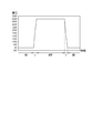
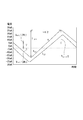
- FIG. 17 is a graph showing changes in the switch voltage (drain-source voltage) when the odd-numbered or even-numbered switch is turned off from on and turned on again.
- the switch voltage is 0V when on and 500V when off.
- ZVT Zero Voltage Transition
- a zero voltage transition that turns on after the switch voltage drops to 0 V is preferable in order to minimize switching loss.
- FIG. 18 is a graph showing the part of the change from OFF to ON in FIG. 17 by enlarging the time on the horizontal axis.
- the dead time ⁇ includes the first half time ⁇ 1 from 500 V to 250 V, and the second half time ⁇ 2 from 250 V to 0 V, which follows. That is, ⁇ ⁇ ⁇ 1 + ⁇ 2 (1) It is.
- the slopes of the first half time ⁇ 1 and the second half time ⁇ 2 are slightly different from each other, and ⁇ 1 ⁇ 2 . Therefore, the dead time ⁇ can be considered separately for the first half time ⁇ 1 and the second half time ⁇ 2 .
- ⁇ 1 Voltage is from 4V out to 2V out
- ⁇ 2 The voltage is from 2V out to 0.
- FIG. 19 is a graph showing the relationship with ZVT in which the length of dead time is set to three types of large, medium and small.
- the dead time ⁇ is smaller than the appropriate value (medium)
- the voltage changes as indicated by the alternate long and short dash line, and the next turn-on starts before reaching 0V. That is, it is not a ZVT.
- the dead time ⁇ is larger than the appropriate value (medium)
- the voltage changes as shown by a solid line and reaches 0V at one end, but then the voltage rises again and eventually the next ON is started as it is. That is, this is not ZVT. Therefore, it can be said that ⁇ indicated by a broken line has an appropriate range that is not too large and not too small.
- FIG. 20 is a circuit diagram in which the diodes D1 to D4 and the bleeder resistors R1 and R2 in FIG. 7 are omitted, and instead, stray capacitances C11 to C14 that the switches SW1 to SW4 respectively have.
- FIG. 20 also shows a current path in the first half time ⁇ 1 .
- the diode D12 is conductive. At this time, current I L1 flowing through the inductor L1, is flowing to the stray capacitance C11 ⁇ C14.
- FIG. 21 is a background diagram similar to FIG. 20, but also shows the current path in the second half time ⁇ 2 .
- the diode D11 is conductive.
- the current I L2 through the inductor L2 has flowed into the floating capacitances C11 ⁇ C14.
- FIG. 22 is a graph illustrating an example of a waveform of a current flowing through the inductors L1 and L2.
- the current waveform can be approximated by a straight line in this way.
- the upper waveform is an IL1 waveform
- the lower waveform is an IL2 waveform.
- the time for each waveform to change from the minimum value to the maximum value is a half period of the switching period T.
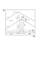
- FIG. 23 is an enlarged view near the top of the waveform of FIG.
- ⁇ 1 (T / 2) + (L / R 3 ) -(1/2) [ ⁇ T + (2L / R 3 ) ⁇ 2 -128LC DS ] 1/2 ... (9) It becomes.
- FIG. 24 is a diagram in which the waveform of FIG. 23 is extended in the time axis direction (right direction).
- ⁇ max be the maximum dead time for not reaching t 0 .
- the dead time ⁇ range should be set as follows. ⁇ 1 + ⁇ 2 ⁇ ⁇ ⁇ ⁇ 0 + ( ⁇ 2/2) + ⁇ 1 ⁇ (15)
- ⁇ 0 , ⁇ 1 and ⁇ 2 are as follows.
- equation (16) is as follows when generalized in consideration of the multi-stage of the previous circuit. Note that equation (15) remains unchanged even when multistage is considered.
- equation (16) is generally as follows It becomes.
- the control unit 3 of the transformer 1 causes the switch to float from the inductor L1 while one of the diodes D11 and D12 (D12) is conducting after the dead time start time.
- the first half time ⁇ 1 determined based on the charge moving to the capacitance C DS and the charge moving from the inductor L2 to the floating capacitance C DS of the switch while the other of the diodes D11 and D12 (D11) is conducting.
- the obtained second half time ⁇ 2 is obtained, and the dead time ⁇ can be determined based on the first half time ⁇ 1 and the second half time ⁇ 2 .
- an appropriate dead time ⁇ can be determined based on the times ⁇ 1 and ⁇ 2 obtained by paying attention to the movement of charges during the dead time, and zero voltage transition (ZVT) can be realized.
- ZVT zero voltage transition
- control unit 3 before the charge transferred to the floating capacitance C DS returns to inductor L1, L2 that end the dead time tau, it is possible to prevent the re-rise of the switch voltage.
- equations (15) to (17) it is possible to clearly define a suitable range of the dead time ⁇ and to realize zero voltage transition with certainty.
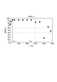
- FIG. 25 is a graph showing the relationship between dead time ⁇ [ns] and efficiency [%] in the case of condition 1.
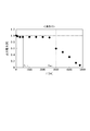
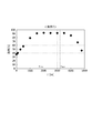
- FIG. 26 is a graph showing the relationship between the dead time ⁇ [ns] in the case of condition 1 and the output power [W] as the transformer.
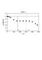
- FIG. 27 is a graph showing the relationship between dead time ⁇ [ns] and efficiency [%] in the case of condition 2.
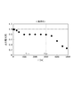
- FIG. 28 is a graph showing the relationship between the dead time ⁇ [ns] in the case of condition 2 and the output power [W] as the transformer.
- FIG. 29 is a graph showing the relationship between dead time ⁇ [ns] and efficiency [%] in condition 3.
- FIG. 30 is a graph showing the relationship between the dead time ⁇ [ns] in the case of condition 3 and the output power [W] as the transformer.
- FIG. 31 is a graph showing the relationship between dead time ⁇ [ns] and efficiency [%] in the case of condition 4.
- FIG. 32 is a graph showing the relationship between the dead time ⁇ [ns] and the output power [W] as the transformer in the case of condition 4.
- FIG. 33 is a graph showing the relationship between dead time ⁇ [ns] and efficiency [%] in the case of condition 5.
- FIG. 34 is a graph showing the relationship between the dead time ⁇ [ns] in the case of condition 5 and the output power [W] as the transformer.
- FIG. 35 is a graph showing the relationship between dead time ⁇ [ns] and efficiency [%] in the case of condition 6.
- FIG. 36 is a graph showing the relationship between the dead time ⁇ [ns] and the output power [W] as the transformer in the case of condition 6.
- FIG. 37 is a graph showing the relationship between dead time ⁇ [ns] and efficiency [%] in the case of condition 7.
- FIG. 38 is a graph showing the relationship between the dead time ⁇ [ns] in the case of condition 7 and the output power [W] as the transformer.
- FIG. 39 is a graph showing the relationship between dead time ⁇ [ns] and efficiency [%] in the case of condition 8.
- FIG. 40 is a graph showing the relationship between the dead time ⁇ [ns] and the output power [W] as the transformer in the case of condition 8.
- FIG. 41 is a graph showing the relationship between dead time ⁇ [ns] and efficiency [%] in the case of condition 9.
- FIG. 42 is a graph showing the relationship between the dead time ⁇ [ns] in the case of condition 9 and the output power [W] as the transformer.
- FIG. 43 is a graph showing the relationship between dead time ⁇ [ns] and efficiency [%] in the case of condition 10.
- FIG. 44 is a graph showing the relationship between the dead time ⁇ [ns] and the output power [W] as the transformer in the case of condition 10.
- the transformer can obtain excellent efficiency and stable high output.
Landscapes
- Engineering & Computer Science (AREA)
- Power Engineering (AREA)
- Inverter Devices (AREA)
- Dc-Dc Converters (AREA)
- Ac-Ac Conversion (AREA)
Abstract
Description
一方、高周波トランスは、寄生容量の影響が回避できず、設計上の困難性がある。
そして、前記前段回路として、(a)2の倍数である複数のスイッチを互いに直列に接続して成り、直列体のいずれか一端側から見て奇数番目のスイッチと偶数番目のスイッチとは交互にオン動作し、全体としては前記電源に対して並列に接続されるスイッチ直列体と、(b)各スイッチの相互接続点及び前記スイッチ直列体の両端点を合計m個のノードとして、前記スイッチ直列体のいずれか一端側から1~mの順番に見たとき、奇数ノードを束ねて第1出力ポートへ導く第1電路、及び、偶数ノードを束ねて第2出力ポートへ導く第2電路の少なくとも一方の電路上に設けられ、少なくとも(m-1)個のノードに対応して存在するキャパシタと、を備え、前記後段回路として、(c)互いに逆極性の通電動作をする一対の半導体素子を互いに直列に接続して成り、直列体の一端が前記第1出力ポートに接続され、他端が前記第2出力ポートに接続される素子直列体と、(d)前記素子直列体の両端点である2個のノードを束ねて前記負荷の一端へ導く第3電路、及び、前記一対の半導体素子の相互接続点である1個のノードを前記負荷の他端へ導く第4電路の少なくとも一方の電路上に設けられ、合計3個のノードのうち少なくとも2個のノードに対応して存在するインダクタと、を備え、さらには、前記スイッチのオン/オフ動作を制御する制御部を備えている変圧装置である。
本発明の実施形態の要旨としては、少なくとも以下のものが含まれる。
前記前段回路として、(a)2の倍数である複数のスイッチを互いに直列に接続して成り、直列体のいずれか一端側から見て奇数番目のスイッチと偶数番目のスイッチとは交互にオン動作し、全体としては前記電源に対して並列に接続されるスイッチ直列体と、(b)各スイッチの相互接続点及び前記スイッチ直列体の両端点を合計m個のノードとして、前記スイッチ直列体のいずれか一端側から1~mの順番に見たとき、奇数ノードを束ねて第1出力ポートへ導く第1電路、及び、偶数ノードを束ねて第2出力ポートへ導く第2電路の少なくとも一方の電路上に設けられ、少なくとも(m-1)個のノードに対応して存在するキャパシタと、を備えている。
また、前記後段回路として、(c)互いに逆極性の通電動作をする一対の半導体素子を互いに直列に接続して成り、直列体の一端が前記第1出力ポートに接続され、他端が前記第2出力ポートに接続される素子直列体と、(d)前記素子直列体の両端点である2個のノードを束ねて前記負荷の一端へ導く第3電路、及び、前記一対の半導体素子の相互接続点である1個のノードを前記負荷の他端へ導く第4電路の少なくとも一方の電路上に設けられ、合計3個のノードのうち少なくとも2個のノードに対応して存在するインダクタと、を備えている。
そして、さらには、前記スイッチのオン/オフ動作を制御する制御部を備えている。
この場合、デッドタイムにおける電荷の移動に着目して求めた時間τ1,τ2に基づいて、適切なデッドタイムτを定め、ゼロ電圧遷移(ZVT:Zero Volt Transition)を実現することができる。
浮遊キャパシタンスに移動した電荷が戻ってくるとスイッチ電圧が再上昇するが、それ以前にデッドタイムτを終わらせることで、スイッチ電圧の再上昇を防止することができる。
τ1+τ2≦τ≦τ0+(τ2/2)+τ1
の関係にあって、
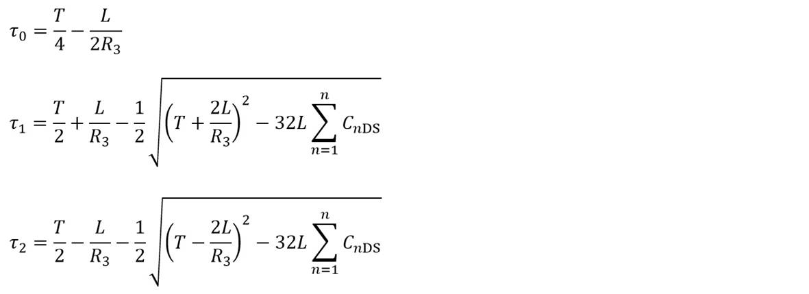
この場合、デッドタイムτの好適範囲を明確に定め、確実にゼロ電圧遷移を実現することができる。
前記スイッチのスイッチング周期をT、前記インダクタのうち前記デッドタイムτに対して支配的なインダクタンスをL1、前記負荷の抵抗値をR3とした場合、前記デッドタイムτは、
τ1+τ2≦τ≦τ0+τ1
の関係にあって、
であり、但し、nは、浮遊キャパシタンスCDSの個数、CnDSは、n番目の浮遊キャパシタンス、上記ルート記号の中の値は符号がプラスであってτ1<τ2である。
以下、実施形態の詳細について図面を参照して説明する。
図1は、本実施形態に係る変圧装置の基本形としての変圧装置1の回路図である。図において、変圧装置1は、交流電源2と、負荷R(Rは、抵抗値でもある。)との間に設けられている。変圧装置1は、一対のキャパシタC1,C2と、一対のインダクタL1,L2と、4つのスイッチSr1,Sr2,Sb1,Sb2と、これらのスイッチSr1,Sr2,Sb1,Sb2のオン/オフを制御する制御部3とを備えている。制御部3のスイッチング周波数は、例えば1MHz程度である。
なお、一対のキャパシタC1,C2のキャパシタンス値は同じ値であってもよいし、互いに異なる値であってもよい。一対のインダクタL1,L2のインダクタンス値についても同様である。
また、一対のインダクタL1,L2は、接続点M2において互いに直列に接続されている。そして、その直列体の両端に、キャパシタC1,C2を介した入力電圧vmが印加され、入力電流imが流れる。負荷Rには、スイッチSr2,Sb2のいずれかがオンのとき電流が流れる。ここで、負荷Rに印加される電圧をvout、変圧装置1から負荷Rに流れる出力電流をioutとする。
一方、図3の(a)は、図1における4つのスイッチSr1,Sr2,Sb1,Sb2のうち、下側にある2つのスイッチSb1,Sb2がオンで、上側にある2つのスイッチSr1,Sr2がオフであるときの、実体接続の状態を示す回路図である。また、図3の(b)は、(a)と同じ回路図を、階段状に書き換えた回路図である。
ここで、入力電圧は1/4となって出力されるのではないかと推定できる。以下、これを理論的に証明する。
なお、計算の簡略化のため、キャパシタC1,C2のキャパシタンスは共に同じ値C、インダクタL1,L2のインダクタンスは共に同じ値L、とする。


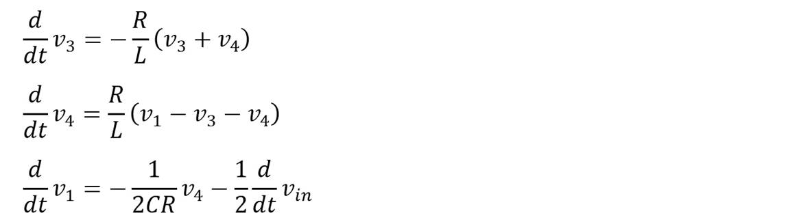


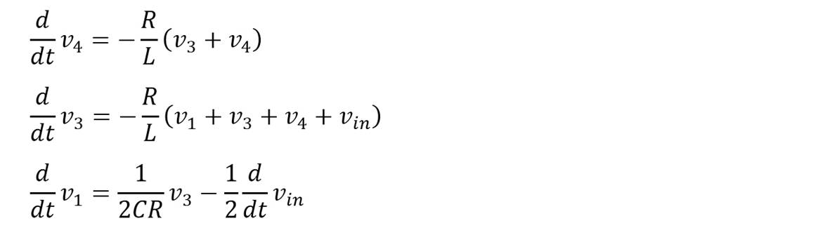
(1)入力電圧の周波数foにおけるLのインピーダンス(リアクタンス)は、抵抗値に対して十分小さい。すなわち、2πfoL<<R、である。不等号で示す差は、例えば、1桁以上、より好ましくは2桁以上の差であることが好ましい。これにより、歪みの少ない、より安定した変圧動作が得られる。
(2)Cのインピーダンス(リアクタンス)は、スイッチング周波数fsにおいては、抵抗値Rに対して十分小さいが、入力電圧の周波数foにおいては、抵抗値に対して十分大きい。すなわち、1/(2πfsC)<<R<<1/(2πfoC)、である。不等号で示す差は、例えば、1桁以上、より好ましくは2桁以上の差であることが好ましい。これにより、歪みの少ない、より安定した変圧動作が得られる。
(3)また、スイッチングの一周期中で、入力電圧は、ほとんど変化しない。
従って、vin(t+Δt)=vin(t) (0 ≦ Δt ≦ 1/fs)
(4)系は定常であり、周期(1/fs)で同等な状態に戻る。
従って、vx(t+(1/fs))≒ vx(t) (x=1,2,3,4)


vin=-2{v3(0)+v4(0)+v3(ΔT)+v4(ΔT)}+v1(0)-v1(ΔT)
ここで、方程式3の3段目の式より、v1(0)-v1(ΔT)=(1/(4fsCR))v4(0)
また、-vout=R(i1+i2)=v3+v4であり、常に成り立つ式であるので、以下の結論式が得られる。

結論式における最下段の式の右辺の第2項は第1項に比べて十分に小さいので無視できる。従って、負荷変動(Rの値の変動)に関係なくvin≒4voutとなり、出力電圧は、入力電圧の約1/4となる。なお、負荷R以外での損失は無いので、出力電流は入力電流の約4倍、入力インピーダンスは抵抗値Rの16倍になる。
図5は、変圧の中間段階での電圧vm、電流imをそれぞれ表す波形図である。これは実際には、スイッチングによるパルス列によって構成され、全体として図示のような波形となる。
また、図6は、上が、変圧装置1からの出力電圧、下が、出力電流をそれぞれ表す波形図である。図4,図6の対比により明らかなように、電圧は1/4に変圧され、それに伴って、電流は4倍となる。
「スイッチ直列体」は、2個のスイッチ(Sr1,Sb1)を互いに直列に接続して成り、直列体のいずれか一端側(例えば上端側)から見て奇数番目のスイッチ(Sr1)と偶数番目のスイッチ(Sb1)とは交互にオン動作し、全体としては電源2に対して並列に接続される。
「キャパシタ(C1,C2)」は、各スイッチの相互接続点(N2)及びスイッチ直列体の両端点(N1,N3)を合計3個のノードとして、スイッチ直列体のいずれか一端側から1~3の順番に見たとき、奇数ノード(N1,N3)を束ねて第1出力ポートPxへ導く第1電路、及び、偶数ノード(N2)を第2出力ポートPyへ導く第2電路の少なくとも一方の電路上に設けられ、2個のノードに対応して存在する。
「素子直列体」は、互いに逆極性の通電動作をする一対の半導体素子(Sr2,Sb2)を互いに直列に接続して成り、直列体の一端が第1出力ポートPxに接続され、他端が第2出力ポートPyに接続される。
「インダクタ(L1,L2)」は、素子直列体の両端点である2個のノード(N11,N13)を束ねて負荷Rの一端へ導く第3電路、及び、一対の半導体素子の相互接続点である1個のノード(N12)を負荷Rの他端へ導く第4電路の少なくとも一方の電路上に設けられ、合計3個のノードのうち2個のノード(N11,N13)に対応して存在する。
次に、上述の基本回路に基づいて、これをさらに実用的に発展させた変圧装置の一例について説明する。
図7は、かかる変圧装置1の回路図である。この変圧装置1は、電源2と負荷Rとの間に設けられ、前段回路1f、後段回路1r、及び、制御部3によって構成される。電源2は、例えば直流電源であり、電圧は1kVである。負荷Rは、等価回路要素として抵抗R3と、キャパシタンスC6とを有する。
後段回路1rは、ダイオードD11,D12と、インダクタL1,L2とを有し、これらは図示のように接続されている。
また、スイッチSW1~SW4について、オン/オフ動作を制御する制御部3が設けられている。
「スイッチ直列体」は、スイッチ(SW1~SW4)を互いに直列に接続して成り、直列体のいずれか一端側(例えば上端側)から見て奇数番目のスイッチ(SW1,SW3)と偶数番目のスイッチ(SW2,SW4)とは交互にオン動作し、全体としては電源2に対して並列に接続される。
「キャパシタ(C1~C5)」は、各スイッチの相互接続点(N2,N3,N4)及びスイッチ直列体の両端点(N1,N5)を合計5個のノードとして、スイッチ直列体のいずれか一端側から1~5の順番に見たとき、奇数ノード(N1,N3,N5)を束ねて第1出力ポートPxへ導く第1電路、及び、偶数ノード(N2,N4)を束ねて第2出力ポートPyへ導く第2電路の少なくとも一方の電路上に設けられ、5個のノードに対応して存在する。
「素子直列体」は、互いに逆極性の通電動作をする一対の半導体素子(D11,D12)を互いに直列に接続して成り、直列体の一端が第1出力ポートPxに接続され、他端が第2出力ポートPyに接続される。
「インダクタ(L1,L2)」は、素子直列体の両端点である2個のノード(N11,N13)を束ねて負荷Rの一端へ導く第3電路、及び、一対の半導体素子の相互接続点である1個のノード(N12)を負荷Rの他端へ導く第4電路の少なくとも一方の電路上に設けられ、合計3個のノードのうち2個のノード(N11,N13)に対応して存在する。
次に、変圧装置1(図1,図7その他)における回路構成のトポロジーのバリエーションについて説明する。
図8は、「2C2L」の変圧装置1における、前段回路1fの要部についての、トポロジーのバリエーションを示す回路図である。(a)~(e)の各図の回路は、一対のスイッチ及び一対のキャパシタ(符号省略)によって構成されている。
なお、いずれの回路もキャパシタは2個であるが、全てのノードN1~N3にそれぞれ対応してキャパシタが存在してもよい。
図9は、後段回路1rの要部についての、トポロジーのバリエーションを示す回路図である。(a)~(e)の各図の回路は、負荷に接続される後段回路1rが、一対のスイッチ及び一対のインダクタ(符号省略)によって構成されている。なお、スイッチに代えて、図7に示すようにダイオードを用いることができる。
なお、いずれの回路もインダクタは2個であるが、全てのノードN11~N13にそれぞれ対応してインダクタが存在してもよい。
図10は、「4C2L」の変圧装置1における前段回路1fの要部の図である。
ここで、スイッチ直列体の一端から見て奇数ノードN1,N3,N5を束ねて第1出力ポートPxに導く第1電路は実線で表し、偶数ノードN2,N4を束ねて第2出力ポートPyに導く第2電路は破線で表している。なお、破線で表しているのは表示の便宜上であり、第1電路と併存する電路である。
このトポロジーは、図7の前段回路1fと同様である。
また、5つのノードN1~N5のうち、第1電路(実線)又は第2電路(破線)で相互に束ねられ、繋がるノード間には直流的な絶縁を実現すべく、少なくとも1つのキャパシタを介していることが必要である。
図11の(a)の回路では、1本に束ねる前の3電路にそれぞれキャパシタが設けられている(図10と同じ)。(b)、(c)、(d)の回路では、1本に束ねる前の3電路のうち2電路にそれぞれキャパシタが設けられ、束ねた後の1本の電路にもキャパシタが設けられる。
図12の(a)、(b)、(c)、(d)の回路では、電路の束ね方が2段階になり、束ねる前又は後にキャパシタが設けられている。
図13の(a)~(e)の回路では、N1,N3,N5のうちいずれか1個のノードは、第1出力ポートPxに直結されている。それ以外のノードは、キャパシタを1個又は2個介して、第1出力ポートPxに接続されている。
(a)、(b)は、第1電路からキャパシタを減らさずに、第2電路からキャパシタを1個減らす場合の回路図である。(a)の場合、ノードN2は第2出力ポートPyに直結されている。ノードN4は、キャパシタを介して第2出力ポートPyに接続されている。(b)の場合、ノードN4は第2出力ポートPyに直結されている。ノードN2は、キャパシタを介して第2出力ポートPyに接続されている。
(c)、(d)、(e)は、第1電路からキャパシタを1個減らし、第2電路からはキャパシタを減らさない場合の回路図である。(c)(図10と同じ)、(d)、(e)のいずれの場合も、ノードN2,N4は共に、1個又は2個のキャパシタを介して第2出力ポートPyに接続されている。
また、降圧比増大方向への変形として「6C2L」も可能である。
図15は、「6C2L」の変圧装置1における前段回路1fの要部の図である。
ここで、スイッチ直列体の一端から見て奇数ノードN1,N3,N5,N7を束ねて第1出力ポートPxに導く第1電路は実線で表し、偶数ノードN2,N4,N6を束ねて第2出力ポートPyに導く第2電路は破線で表している。なお、破線で表しているのは表示の便宜上であり、第1電路と併存する電路である。
また、7つのノードN1~N7のうち、第1電路(実線)又は第2電路(破線)で相互に束ねられ、繋がるノード間には直流的な絶縁を実現すべく、少なくとも1つのキャパシタを介していることが必要である。
なお、さらに、「8C」以上にも同様に拡張することができる。
以上例示した各種の回路から、前段回路1fのトポロジーは以下のように表現できる。
前段回路1f(図1,図8,図10~16)は、(a)2の倍数である複数のスイッチを互いに直列に接続して成り、直列体のいずれか一端側から見て奇数番目のスイッチと偶数番目のスイッチとは交互にオン動作し、全体としては電源に対して並列に接続されるスイッチ直列体と、(b)各スイッチの相互接続点及びスイッチ直列体の両端点を合計m個のノードとして、スイッチ直列体のいずれか一端側から1~mの順番に見たとき、奇数ノードを束ねて第1出力ポートへ導く第1電路、及び、偶数ノードを束ねて第2出力ポートへ導く第2電路の少なくとも一方の電路上に設けられ、少なくとも(m-1)個のノードに対応して存在するキャパシタと、を備えている。
なお、後段回路1rの半導体素子がダイオードの場合は、通電方向を互いに逆向きにして直列接続することにより素子直列体を構成することができる。半導体素子がスイッチの場合は、一対のスイッチを直列接続して素子直列体を構成し、一対のスイッチを交互にオン動作させる。
次にデッドタイムの設計について説明する。デッドタイムとは、例えば、図7において奇数番目のスイッチSW1,SW3と、偶数番目のスイッチSW2,SW4とが交互のオンになる合間の、全てのスイッチに対する制御がオフになった瞬間から、いずれか一方のスイッチの制御がオンになるまでの過渡的な時間である。
τ≧τ1+τ2 ・・・(1)
である。前半時間τ1と後半時間τ2とは勾配が互いに少し異なり、τ1<τ2である。従って、デッドタイムτを、前半時間τ1と後半時間τ2とに分けて考察することができる。変圧装置1の出力電圧125VをVoutとすると、
τ1:電圧が、4Vout~2Voutまで、
τ2:電圧が、2Vout~0まで、である。
IQ=IL2+IR=IL1
である。
IQ=IL1-IR=IL2
である。従って、IL2は、IL1より小さい。
(近似条件1)
まず、降圧比は1/8で一定とする。すなわち、変圧装置1の入力電圧をVin、出力電圧をVoutとすると、
Vout≒Vin/8=125[V]
である。
(近似条件2)
インダクタL1,L2の両端の電圧波形はデューティ比50%の矩形波である。
(近似条件3)
そして、インダクタL1,L2の両端の電圧VL1,VL2の絶対値は、出力電圧である。すなわち、電圧VLの最大値をVLmax、最小値をVLminとすると、
VLmax≒Vout
VLmin≒-Vout
である。また、計算の簡略化のため、
VL1≒VL2≒±Vout
とする。
VL=L(dIL(t)/dt)=L・a
である。aは直線の傾きである。
従って、
a=Vout/L ・・・(2)
である。
また、ピーク・トゥー・ピークのILp-pは、
ILp-p=a(T/2)である。従って、
ILp-p=T・Vout/2L ・・・(3)
である。
Q1={(ILp-p/2)+(Vout/2R3)}τ1
-(τ1/2)・(aτ1/2) ・・・(4)
である。また、後半時間τ2の間に浮遊キャパシタンスCDSに流れ込む電荷Q2は、図の右側のハッチング面積となる。すなわち、
Q2={(ILp-p/2)-(Vout/2R3)}τ2
-(τ2/2)・(aτ2/2) ・・・(5)
である。
Q1=(Vout・τ1/2){(T/2L)+(1/R3)}
-(Vout・τ12/4L) ・・・(6)
となる。
また、式(5)のQ2に、式(2)、(3)を代入して整理すると、
Q2=(Vout・τ2/2){(T/2L)-(1/R3)}
-(Vout・τ22/4L) ・・・(7)
となる。
Q1=4CDS・2Vout=8CDS・Vout ・・・(8)
である。式(6)、(8)から得られる二次方程式をτ1について解くと、
τ1=(T/2)+(L/R3)
-(1/2)[{T+(2L/R3)}2-128LCDS]1/2
・・・(9)
となる。
Q2=4CDS・2Vout=8CDS・Vout ・・・(10)
である。式(7)、(10)から得られる二次方程式をτ2について解くと、
τ2=(T/2)-(L/R3)
-(1/2)[{T-(2L/R3)}2-128LCDS]1/2
・・・(11)
となる。
図24は、図23の波形を時間軸方向(右方向)へ延長した図である。後半時間τ2の後半領域に入ると、電流の勾配は(-a)となる。従って、IL2=0となる時刻t0が存在する。時刻t0を過ぎると、マイナスの電流が流れることになる。これは、時刻t0以降に、右下のハッチングの部分の電荷が戻ってくることを意味している。もしそうなると、スイッチ電圧が再上昇するので、デッドタイムτは、t0に達しないようにしなければならない。t0に達しないためのデッドタイムの最大値をτmaxとする。
{(ILp-p/2)-(Vout/2R3)}-aτ0=0 ・・・(12)
である。式(12)に、式(2)、(3)を代入してτ0について解くと、
τ0=(T/4)-(L/2R3) ・・・(13)
となる。ここで、図24より、
τmax=τ0+(τ2/2)+τ1 ・・・(14)
である。式(13)、(14)より、
τmax=(T/4)-(L/2R3)+(τ2/2)+τ1
・・・(14a)
となる。
なお、スイッチングのオン時間を確保するために、τmaxは、τmax<(T/2)でなければならないことは言うまでもない。
τ1+τ2≦τ≦τ0+(τ2/2)+τ1 ・・・(15)
ここで、τ0,τ1,τ2は、以下の通りである。

浮遊キャパシタンスCDSの個数(すなわちスイッチ直列体を構成するスイッチの個数と同じ)をn、1から順番に数えてn番目の浮遊キャパシタンスをCnDSとすると、式(16)は以下のように一般化される。

なお、上記ルート記号の中の値は符号がプラスであってτ1<τ2である。
デッドタイムτの範囲は前段回路のトポロジーによらず、後段回路のトポロジーで決まることがわかっている。後段回路が、図9の(b)であるときは、τは、上記の式(15)及び式(17)により、与えられる。
τ1+τ2≦τ≦τ0+τ1 ・・・(15a)
ここで、τ0,τ1,τ2は、以下の通りである。

前述のように、後段のトポロジーが図9の(a),(c),(d),(e)のときは、デッドタイムτに対して支配的なインダクタンスはL1であるため、式(17a)に登場するインダクタンスはL1のみである。
以上、詳述したように、例えば図7において、変圧装置1の制御部3は、デッドタイム開始時刻後、ダイオードD11,D12の一方(D12)が導通している間にインダクタL1からスイッチの浮遊キャパシタンスCDSに移動する電荷に基づいて求められる前半時間τ1と、ダイオードD11,D12の他方(D11)が導通している間にインダクタL2からスイッチの浮遊キャパシタンスCDSに移動する電荷に基づいて求められる後半時間τ2とを求め、前半時間τ1及び後半時間τ2に基づいて、デッドタイムτを定めることができる。
これにより、デッドタイムにおける電荷の移動に着目して求めた時間τ1,τ2に基づいて、適切なデッドタイムτを定め、ゼロ電圧遷移(ZVT)を実現することができる。
また、上記式(15)~(17)により、デッドタイムτの好適範囲を明確に定め、確実にゼロ電圧遷移を実現することができる。
次に、上記の範囲でデッドタイムτを設計した場合の変圧装置について、その性能を検証した結果を以下に示す。
回路構成:「2C2L」
インダクタL1,L2のインダクタンスL=15[mH]
負荷の抵抗R3=15625[Ω]
浮遊キャパシタンスCDS=5[pF]
上記の条件1の場合、式(15)、(17)に基づいてデッドタイムτの最小値及び最大値を計算すると、
最小値τmin=253[ns]
最大値τmax=2197[ns]
となる。
図26は、条件1の場合のデッドタイムτ[ns]と変圧装置としての出力電力[W]との関係を示すグラフである。上記計算上のτmin及びτmaxをグラフ上で示すと、グラフの特性上で安定した高出力となる範囲と一致していることがわかる。
回路構成:「2C2L」
インダクタL1,L2のインダクタンスL=15[mH]
負荷の抵抗R3=7000[Ω]
浮遊キャパシタンスCDS=5[pF]
上記の条件2の場合、式(15)、(17)に基づいてデッドタイムτの最小値及び最大値を計算すると、
最小値τmin=303[ns]
最大値τmax=1622[ns]
となる。
図28は、条件2の場合のデッドタイムτ[ns]と変圧装置としての出力電力[W]との関係を示すグラフである。上記計算上のτmin及びτmaxをグラフ上で示すと、グラフの特性上で安定した高出力となる範囲と一致していることがわかる。
回路構成:「2C2L」
インダクタL1,L2のインダクタンスL=15[mH]
負荷の抵抗R3=15625[Ω]
浮遊キャパシタンスCDS=10[pF]
上記の条件3の場合、式(15)、(17)に基づいてデッドタイムτの最小値及び最大値を計算すると、
最小値τmin=514[ns]
最大値τmax=2379[ns]
となる。
図30は、条件3の場合のデッドタイムτ[ns]と変圧装置としての出力電力[W]との関係を示すグラフである。上記計算上のτmin及びτmaxをグラフ上で示すと、グラフの特性上で安定した高出力となる範囲と一致していることがわかる。
回路構成:「2C2L」
インダクタL1,L2のインダクタンスL=7.5[mH]
負荷の抵抗R3=15625[Ω]
浮遊キャパシタンスCDS=5[pF]
上記の条件4の場合、式(15)、(17)に基づいてデッドタイムτの最小値及び最大値を計算すると、
最小値τmin=122[ns]
最大値τmax=2348[ns]
となる。
図32は、条件4の場合のデッドタイムτ[ns]と変圧装置としての出力電力[W]との関係を示すグラフである。上記計算上のτmin及びτmaxをグラフ上で示すと、グラフの特性上で安定した高出力となる範囲と一致していることがわかる。
回路構成:「6C2L」
インダクタL1,L2のインダクタンスL=15[mH]
負荷の抵抗R3=15625[Ω]
浮遊キャパシタンスCDS=5[pF]
上記の条件5の場合、式(15)、(17)に基づいてデッドタイムτの最小値及び最大値を計算すると、
最小値τmin=783[ns]
最大値τmax=2567[ns]
となる。
図34は、条件5の場合のデッドタイムτ[ns]と変圧装置としての出力電力[W]との関係を示すグラフである。上記計算上のτmin及びτmaxをグラフ上で示すと、グラフの特性上で安定した高出力となる範囲と一致していることがわかる。
回路構成:「6C2L」
インダクタL1,L2のインダクタンスL=15[mH]
負荷の抵抗R3=7000[Ω]
浮遊キャパシタンスCDS=5[pF]
上記の条件6の場合、式(15)、(17)に基づいてデッドタイムτの最小値及び最大値を計算すると、
最小値τmin=978[ns]
最大値τmax=2046[ns]
となる。
図36は、条件6の場合のデッドタイムτ[ns]と変圧装置としての出力電力[W]との関係を示すグラフである。上記計算上のτmin及びτmaxをグラフ上で示すと、グラフの特性上で安定した高出力となる範囲と一致していることがわかる。
回路構成:「6C2L」
インダクタL1,L2のインダクタンスL=15[mH]
負荷の抵抗R3=15625[Ω]
浮遊キャパシタンスCDS=10[pF]
上記の条件7の場合、式(15)、(17)に基づいてデッドタイムτの最小値及び最大値を計算すると、
最小値τmin=1658[ns]
最大値τmax=3168[ns]
となる。
図38は、条件7の場合のデッドタイムτ[ns]と変圧装置としての出力電力[W]との関係を示すグラフである。上記計算上のτmin及びτmaxをグラフ上で示すと、グラフの特性上で安定した高出力となる範囲と一致していることがわかる。
回路構成:「6C2L」
インダクタL1,L2のインダクタンスL=7.5[mH]
負荷の抵抗R3=15625[Ω]
浮遊キャパシタンスCDS=5[pF]
上記の条件8の場合、式(15)、(17)に基づいてデッドタイムτの最小値及び最大値を計算すると、
最小値τmin=370[ns]
最大値τmax=2528[ns]
となる。
図40は、条件8の場合のデッドタイムτ[ns]と変圧装置としての出力電力[W]との関係を示すグラフである。上記計算上のτmin及びτmaxをグラフ上で示すと、グラフの特性上で安定した高出力となる範囲と一致していることがわかる。
回路構成:「4C2L」
インダクタL1,L2のインダクタンスL=15[mH]
負荷の抵抗R3=15625[Ω]
浮遊キャパシタンスCDS:17[pF],10[pF],10[pF],3[pF]
全体としての浮遊キャパシタンスΣCDS:40[pF]
上記の条件9の場合、式(15)、(17)に基づいてデッドタイムτの最小値及び最大値を計算すると、
最小値τmin=1063[ns]
最大値τmax=2760[ns]
となる。
図42は、条件9の場合のデッドタイムτ[ns]と変圧装置としての出力電力[W]との関係を示すグラフである。上記計算上のτmin及びτmaxをグラフ上で示すと、グラフの特性上で安定した高出力となる範囲と一致していることがわかる。
回路構成:「4C2L」
インダクタL1,L2のインダクタンスL=15[mH]
負荷の抵抗R3=15625[Ω]
浮遊キャパシタンスCDS:12[pF],5[pF],15[pF],8[pF]
全体としての浮遊キャパシタンスΣCDS:40[pF]
上記の条件10の場合、式(15)、(17)に基づいてデッドタイムτの最小値及び最大値を計算すると、
最小値τmin=1063[ns]
最大値τmax=2760[ns]
となる。
図44は、条件10の場合のデッドタイムτ[ns]と変圧装置としての出力電力[W]との関係を示すグラフである。上記計算上のτmin及びτmaxをグラフ上で示すと、グラフの特性上で安定した高出力となる範囲と一致していることがわかる。
なお、今回開示された実施の形態はすべての点で例示であって制限的なものではないと考えられるべきである。本発明の範囲は特許請求の範囲によって示され、特許請求の範囲と均等の意味及び範囲内での全ての変更が含まれることが意図される。
1f 前段回路
1r 後段回路
2 交流電源、電源
3 制御部
4 スイッチ装置
C1~C5 キャパシタ
C6 キャパシタンス
D1~D4,D11,D12 ダイオード
L1,L2 インダクタ
M1,M2 接続点
N1~N7,N11~N13 ノード
Px 第1出力ポート
Py 第2出力ポート
R 負荷
R1,R2 ブリーダ抵抗
R3 抵抗
Sr1,Sr2,Sb1,Sb2 スイッチ
SW1~SW4 スイッチ
Claims (5)
- 電源と負荷との間に設けられる変圧装置であって、前段回路及び後段回路によって構成され、
前記前段回路として、
2の倍数である複数のスイッチを互いに直列に接続して成り、直列体のいずれか一端側から見て奇数番目のスイッチと偶数番目のスイッチとは交互にオン動作し、全体としては前記電源に対して並列に接続されるスイッチ直列体と、
各スイッチの相互接続点及び前記スイッチ直列体の両端点を合計m個のノードとして、前記スイッチ直列体のいずれか一端側から1~mの順番に見たとき、奇数ノードを束ねて第1出力ポートへ導く第1電路、及び、偶数ノードを束ねて第2出力ポートへ導く第2電路の少なくとも一方の電路上に設けられ、少なくとも(m-1)個のノードに対応して存在するキャパシタと、を備え、
前記後段回路として、
互いに逆極性の通電動作をする一対の半導体素子を互いに直列に接続して成り、直列体の一端が前記第1出力ポートに接続され、他端が前記第2出力ポートに接続される素子直列体と、
前記素子直列体の両端点である2個のノードを束ねて前記負荷の一端へ導く第3電路、及び、前記一対の半導体素子の相互接続点である1個のノードを前記負荷の他端へ導く第4電路の少なくとも一方の電路上に設けられ、合計3個のノードのうち少なくとも2個のノードに対応して存在するインダクタと、を備え、
前記スイッチのオン/オフ動作を制御する制御部を備えている変圧装置。 - 前記奇数番目のスイッチ及び前記偶数番目のスイッチに対する制御がいずれもオフになったデッドタイム開始時刻から、いずれか一方のスイッチに対する制御がオンになるデッドタイム終了時刻までの時間をデッドタイムτとすると、
前記制御部は、前記デッドタイム開始時刻後、前記半導体素子の一方が導通している間に前記インダクタから前記スイッチの浮遊キャパシタンスに移動する電荷に基づいて求められる前半時間τ1と、前記半導体素子の他方が導通している間に前記インダクタから前記スイッチの浮遊キャパシタンスに移動する電荷に基づいて求められる後半時間τ2とを求め、前半時間τ1及び後半時間τ2に基づいて、前記デッドタイムτを定める請求項1に記載の変圧装置。 - 前記制御部は、前記浮遊キャパシタンスに移動した電荷が前記インダクタに戻る以前に前記デッドタイムτを終わらせる請求項2に記載の変圧装置。
- 前記スイッチのスイッチング周期をT、前記インダクタのインダクタンスをL、前記負荷の抵抗値をR3とした場合、前記デッドタイムτは、
τ1+τ2≦τ≦τ0+(τ2/2)+τ1
の関係にあって、
であり、但し、nは、浮遊キャパシタンスCDSの個数、CnDSは、n番目の浮遊キャパシタンス、上記ルート記号の中の値は符号がプラスであってτ1<τ2である請求項3に記載の変圧装置。
- 前記スイッチのスイッチング周期をT、前記インダクタのうち前記デッドタイムに対して支配的なインダクタンスをL1、前記負荷の抵抗値をR3とした場合、前記デッドタイムτは、
τ1+τ2≦τ≦τ0+τ1
の関係にあって、
であり、但し、nは、浮遊キャパシタンスCDSの個数、CnDSは、n番目の浮遊キャパシタンス、上記ルート記号の中の値は符号がプラスであってτ1<τ2である請求項3に記載の変圧装置。
Priority Applications (4)
| Application Number | Priority Date | Filing Date | Title |
|---|---|---|---|
| EP15857728.8A EP3217527B1 (en) | 2014-11-05 | 2015-10-09 | Transformer |
| US15/509,296 US10122288B2 (en) | 2014-11-05 | 2015-10-09 | Transformer composed of a front stage circuit and a rear stage circuit |
| CN201580054952.4A CN107112908B (zh) | 2014-11-05 | 2015-10-09 | 变压器 |
| KR1020177007914A KR20170081165A (ko) | 2014-11-05 | 2015-10-09 | 변압 장치 |
Applications Claiming Priority (2)
| Application Number | Priority Date | Filing Date | Title |
|---|---|---|---|
| JP2014-225426 | 2014-11-05 | ||
| JP2014225426A JP6359950B2 (ja) | 2014-11-05 | 2014-11-05 | 変圧装置 |
Publications (1)
| Publication Number | Publication Date |
|---|---|
| WO2016072213A1 true WO2016072213A1 (ja) | 2016-05-12 |
Family
ID=55908940
Family Applications (1)
| Application Number | Title | Priority Date | Filing Date |
|---|---|---|---|
| PCT/JP2015/078736 Ceased WO2016072213A1 (ja) | 2014-11-05 | 2015-10-09 | 変圧装置 |
Country Status (7)
| Country | Link |
|---|---|
| US (1) | US10122288B2 (ja) |
| EP (1) | EP3217527B1 (ja) |
| JP (1) | JP6359950B2 (ja) |
| KR (1) | KR20170081165A (ja) |
| CN (1) | CN107112908B (ja) |
| TW (1) | TWI666866B (ja) |
| WO (1) | WO2016072213A1 (ja) |
Families Citing this family (1)
| Publication number | Priority date | Publication date | Assignee | Title |
|---|---|---|---|---|
| JPH089477B2 (ja) | 1989-05-17 | 1996-01-31 | 日本レヂボン株式会社 | 手すりベルトのコーティング方法 |
Citations (3)
| Publication number | Priority date | Publication date | Assignee | Title |
|---|---|---|---|---|
| JP2010074931A (ja) * | 2008-09-18 | 2010-04-02 | Sumitomo Electric Ind Ltd | 電圧変換回路 |
| JP2013146181A (ja) * | 2011-12-16 | 2013-07-25 | Asahi Kasei Electronics Co Ltd | チャージ・ポンプ回路および負荷駆動システム |
| WO2015037455A1 (ja) * | 2013-09-12 | 2015-03-19 | 住友電気工業株式会社 | 変圧装置 |
Family Cites Families (30)
| Publication number | Priority date | Publication date | Assignee | Title |
|---|---|---|---|---|
| FR1064891A (fr) | 1952-10-18 | 1954-05-18 | Csf | Perfectionnements aux réseaux transformateurs d'impédances |
| US4203151A (en) | 1978-09-21 | 1980-05-13 | Exxon Research & Engineering Co. | High-voltage converter circuit |
| US5570062A (en) | 1994-10-12 | 1996-10-29 | Ericsson Ge Mobile Communications Inc. | AM-FM transmitter power amplifier using class-BC |
| US5850337A (en) | 1997-07-25 | 1998-12-15 | Lucent Technologies Inc. | Magnetic-free DC/DC converter and method of operation thereof |
| US6462962B1 (en) * | 2000-09-08 | 2002-10-08 | Slobodan Cuk | Lossless switching DC-to-DC converter |
| JP3391773B2 (ja) | 2000-09-14 | 2003-03-31 | 敏久 清水 | イミタンス変換回路及びこれを使用したコンバータ |
| FR2818463B1 (fr) | 2000-12-18 | 2003-02-28 | Eisenmann France Sarl | Generateur de haute tension pour equipement de peinture electrostatique |
| US7209370B2 (en) * | 2003-08-09 | 2007-04-24 | Astec International Limited | Circuit for reducing losses at light load in a soft switching full bridge converter |
| CN2798411Y (zh) | 2004-12-02 | 2006-07-19 | 吴观晖 | 一种使用电场耦合变压器构成的直流变换器 |
| EP2025051B1 (en) | 2006-06-06 | 2014-12-31 | Ideal Power Inc. | Universal power converter |
| DE102007030577A1 (de) | 2007-06-29 | 2009-01-02 | Sma Solar Technology Ag | Wechselrichter zur Einspeisung elektrischer Energie in ein Energieversorgungsnetz |
| EP2023475B1 (de) * | 2007-08-04 | 2016-10-12 | SMA Solar Technology AG | Wechselrichter für eine geerdete Gleichspannungsquelle, insbesondere einen Photovoltaikgenerator |
| AT505801B1 (de) | 2007-09-20 | 2012-09-15 | Siemens Ag | Verfahren zum betrieb eines elektronisch gesteuerten wechselrichters |
| US8212541B2 (en) | 2008-05-08 | 2012-07-03 | Massachusetts Institute Of Technology | Power converter with capacitive energy transfer and fast dynamic response |
| JP5248615B2 (ja) * | 2009-03-05 | 2013-07-31 | 東芝三菱電機産業システム株式会社 | 無停電電源装置 |
| CN102158096B (zh) * | 2011-05-11 | 2013-11-20 | 南京博兰得电子科技有限公司 | 一种非隔离式谐振变换器 |
| DE202011102068U1 (de) | 2011-06-07 | 2012-09-10 | Voltwerk Electronics Gmbh | Hochsetzsteller |
| EP2727230A2 (en) * | 2011-07-01 | 2014-05-07 | Linak A/S | Power supply with output rectifier |
| JP5927826B2 (ja) | 2011-09-28 | 2016-06-01 | 日産自動車株式会社 | 非接触給電装置 |
| TWI488417B (zh) * | 2011-11-29 | 2015-06-11 | Chung Ming Young | 可應用於再生能源之非隔離單相多階變頻器系統 |
| US9248747B2 (en) * | 2011-11-29 | 2016-02-02 | Valeo Systemes De Controle Moteur | Converter for an electrical circuit designed to supply electrical propulsion power on board a motor vehicle |
| US8829866B2 (en) | 2011-12-14 | 2014-09-09 | Volterra Semiconductor Corporation | DC to DC converter designed to mitigate problems associated with low duty cycle operation |
| CN102412728B (zh) * | 2011-12-23 | 2014-09-17 | 航天长峰朝阳电源有限公司 | 链式大功率正向升压直流变换电路 |
| JP5598513B2 (ja) * | 2012-08-29 | 2014-10-01 | 株式会社村田製作所 | 電力系統連系インバータ装置 |
| JP5626293B2 (ja) * | 2012-08-29 | 2014-11-19 | 株式会社村田製作所 | インバータ装置 |
| US8693224B1 (en) | 2012-11-26 | 2014-04-08 | Arctic Sand Technologies Inc. | Pump capacitor configuration for switched capacitor circuits |
| JP5878495B2 (ja) * | 2013-06-11 | 2016-03-08 | 株式会社豊田中央研究所 | 電動車両の電源システム |
| JP5727561B2 (ja) * | 2013-08-29 | 2015-06-03 | 住友電気工業株式会社 | 変圧装置 |
| JP5695712B2 (ja) | 2013-08-29 | 2015-04-08 | 住友電気工業株式会社 | 変圧装置 |
| CN105556821B (zh) | 2013-09-19 | 2018-11-13 | 飞利浦照明控股有限公司 | 具有辅助输出的特别用于发光二极管的紧凑驱动器 |
-
2014
- 2014-11-05 JP JP2014225426A patent/JP6359950B2/ja active Active
-
2015
- 2015-10-09 WO PCT/JP2015/078736 patent/WO2016072213A1/ja not_active Ceased
- 2015-10-09 US US15/509,296 patent/US10122288B2/en active Active
- 2015-10-09 CN CN201580054952.4A patent/CN107112908B/zh not_active Expired - Fee Related
- 2015-10-09 EP EP15857728.8A patent/EP3217527B1/en active Active
- 2015-10-09 KR KR1020177007914A patent/KR20170081165A/ko not_active Withdrawn
- 2015-10-29 TW TW104135621A patent/TWI666866B/zh active
Patent Citations (3)
| Publication number | Priority date | Publication date | Assignee | Title |
|---|---|---|---|---|
| JP2010074931A (ja) * | 2008-09-18 | 2010-04-02 | Sumitomo Electric Ind Ltd | 電圧変換回路 |
| JP2013146181A (ja) * | 2011-12-16 | 2013-07-25 | Asahi Kasei Electronics Co Ltd | チャージ・ポンプ回路および負荷駆動システム |
| WO2015037455A1 (ja) * | 2013-09-12 | 2015-03-19 | 住友電気工業株式会社 | 変圧装置 |
Non-Patent Citations (1)
| Title |
|---|
| See also references of EP3217527A4 * |
Also Published As
| Publication number | Publication date |
|---|---|
| CN107112908B (zh) | 2019-05-14 |
| US20170288559A1 (en) | 2017-10-05 |
| JP2016092981A (ja) | 2016-05-23 |
| JP6359950B2 (ja) | 2018-07-18 |
| EP3217527B1 (en) | 2019-11-20 |
| TWI666866B (zh) | 2019-07-21 |
| EP3217527A1 (en) | 2017-09-13 |
| CN107112908A (zh) | 2017-08-29 |
| KR20170081165A (ko) | 2017-07-11 |
| TW201624905A (zh) | 2016-07-01 |
| US10122288B2 (en) | 2018-11-06 |
| EP3217527A4 (en) | 2018-07-04 |
Similar Documents
| Publication | Publication Date | Title |
|---|---|---|
| US20080019158A1 (en) | Multi-phase buck converter with a plurality of coupled inductors | |
| JP5695782B1 (ja) | 変圧装置 | |
| WO2014174809A1 (ja) | 双方向dc/dcコンバータ | |
| JP5727561B2 (ja) | 変圧装置 | |
| JP5695712B2 (ja) | 変圧装置 | |
| US9577528B2 (en) | Power converter | |
| JP6297963B2 (ja) | 変圧装置 | |
| JP6359950B2 (ja) | 変圧装置 | |
| CN109120168B (zh) | 功率变换装置 | |
| JP7247247B2 (ja) | 電力変換装置 | |
| KR100998064B1 (ko) | Zcs를 위해 누설 인덕터를 zcs용 인덕터로 사용하는 dc-dc 컨버터 | |
| JP6905452B2 (ja) | 変圧装置 | |
| Laugner et al. | Influence of the parasitic series inductance of the coupling capacitor of a SEPIC to the coil current waveforms with coupled inductors | |
| JP6144709B2 (ja) | 変圧装置 | |
| Adler et al. | Design and operation of a 700 kV arbitrary waveform generator | |
| KR101472448B1 (ko) | 고전압용 dc/dc 컨버터 |
Legal Events
| Date | Code | Title | Description |
|---|---|---|---|
| 121 | Ep: the epo has been informed by wipo that ep was designated in this application |
Ref document number: 15857728 Country of ref document: EP Kind code of ref document: A1 |
|
| REEP | Request for entry into the european phase |
Ref document number: 2015857728 Country of ref document: EP |
|
| WWE | Wipo information: entry into national phase |
Ref document number: 2015857728 Country of ref document: EP |
|
| WWE | Wipo information: entry into national phase |
Ref document number: 15509296 Country of ref document: US |
|
| ENP | Entry into the national phase |
Ref document number: 20177007914 Country of ref document: KR Kind code of ref document: A |
|
| NENP | Non-entry into the national phase |
Ref country code: DE |