WO2016072276A1 - 半導体発光素子 - Google Patents
半導体発光素子 Download PDFInfo
- Publication number
- WO2016072276A1 WO2016072276A1 PCT/JP2015/079805 JP2015079805W WO2016072276A1 WO 2016072276 A1 WO2016072276 A1 WO 2016072276A1 JP 2015079805 W JP2015079805 W JP 2015079805W WO 2016072276 A1 WO2016072276 A1 WO 2016072276A1
- Authority
- WO
- WIPO (PCT)
- Prior art keywords
- layer
- base
- light emitting
- quantum well
- semiconductor
- Prior art date
- Legal status (The legal status is an assumption and is not a legal conclusion. Google has not performed a legal analysis and makes no representation as to the accuracy of the status listed.)
- Ceased
Links
Images


Classifications
-
- H—ELECTRICITY
- H10—SEMICONDUCTOR DEVICES; ELECTRIC SOLID-STATE DEVICES NOT OTHERWISE PROVIDED FOR
- H10K—ORGANIC ELECTRIC SOLID-STATE DEVICES
- H10K85/00—Organic materials used in the body or electrodes of devices covered by this subclass
- H10K85/30—Coordination compounds
- H10K85/321—Metal complexes comprising a group IIIA element, e.g. Tris (8-hydroxyquinoline) gallium [Gaq3]
- H10K85/326—Metal complexes comprising a group IIIA element, e.g. Tris (8-hydroxyquinoline) gallium [Gaq3] comprising gallium
-
- H—ELECTRICITY
- H10—SEMICONDUCTOR DEVICES; ELECTRIC SOLID-STATE DEVICES NOT OTHERWISE PROVIDED FOR
- H10H—INORGANIC LIGHT-EMITTING SEMICONDUCTOR DEVICES HAVING POTENTIAL BARRIERS
- H10H20/00—Individual inorganic light-emitting semiconductor devices having potential barriers, e.g. light-emitting diodes [LED]
- H10H20/80—Constructional details
- H10H20/81—Bodies
- H10H20/819—Bodies characterised by their shape, e.g. curved or truncated substrates
- H10H20/821—Bodies characterised by their shape, e.g. curved or truncated substrates of the light-emitting regions, e.g. non-planar junctions
-
- H—ELECTRICITY
- H10—SEMICONDUCTOR DEVICES; ELECTRIC SOLID-STATE DEVICES NOT OTHERWISE PROVIDED FOR
- H10H—INORGANIC LIGHT-EMITTING SEMICONDUCTOR DEVICES HAVING POTENTIAL BARRIERS
- H10H20/00—Individual inorganic light-emitting semiconductor devices having potential barriers, e.g. light-emitting diodes [LED]
- H10H20/80—Constructional details
- H10H20/81—Bodies
- H10H20/811—Bodies having quantum effect structures or superlattices, e.g. tunnel junctions
- H10H20/812—Bodies having quantum effect structures or superlattices, e.g. tunnel junctions within the light-emitting regions, e.g. having quantum confinement structures
-
- H—ELECTRICITY
- H10—SEMICONDUCTOR DEVICES; ELECTRIC SOLID-STATE DEVICES NOT OTHERWISE PROVIDED FOR
- H10H—INORGANIC LIGHT-EMITTING SEMICONDUCTOR DEVICES HAVING POTENTIAL BARRIERS
- H10H20/00—Individual inorganic light-emitting semiconductor devices having potential barriers, e.g. light-emitting diodes [LED]
- H10H20/80—Constructional details
- H10H20/81—Bodies
- H10H20/813—Bodies having a plurality of light-emitting regions, e.g. multi-junction LEDs or light-emitting devices having photoluminescent regions within the bodies
-
- H—ELECTRICITY
- H10—SEMICONDUCTOR DEVICES; ELECTRIC SOLID-STATE DEVICES NOT OTHERWISE PROVIDED FOR
- H10H—INORGANIC LIGHT-EMITTING SEMICONDUCTOR DEVICES HAVING POTENTIAL BARRIERS
- H10H20/00—Individual inorganic light-emitting semiconductor devices having potential barriers, e.g. light-emitting diodes [LED]
- H10H20/80—Constructional details
- H10H20/81—Bodies
- H10H20/819—Bodies characterised by their shape, e.g. curved or truncated substrates
-
- H—ELECTRICITY
- H10—SEMICONDUCTOR DEVICES; ELECTRIC SOLID-STATE DEVICES NOT OTHERWISE PROVIDED FOR
- H10H—INORGANIC LIGHT-EMITTING SEMICONDUCTOR DEVICES HAVING POTENTIAL BARRIERS
- H10H20/00—Individual inorganic light-emitting semiconductor devices having potential barriers, e.g. light-emitting diodes [LED]
- H10H20/80—Constructional details
- H10H20/81—Bodies
- H10H20/822—Materials of the light-emitting regions
- H10H20/824—Materials of the light-emitting regions comprising only Group III-V materials, e.g. GaP
- H10H20/825—Materials of the light-emitting regions comprising only Group III-V materials, e.g. GaP containing nitrogen, e.g. GaN
-
- H—ELECTRICITY
- H10—SEMICONDUCTOR DEVICES; ELECTRIC SOLID-STATE DEVICES NOT OTHERWISE PROVIDED FOR
- H10H—INORGANIC LIGHT-EMITTING SEMICONDUCTOR DEVICES HAVING POTENTIAL BARRIERS
- H10H20/00—Individual inorganic light-emitting semiconductor devices having potential barriers, e.g. light-emitting diodes [LED]
- H10H20/80—Constructional details
- H10H20/83—Electrodes
-
- H—ELECTRICITY
- H10—SEMICONDUCTOR DEVICES; ELECTRIC SOLID-STATE DEVICES NOT OTHERWISE PROVIDED FOR
- H10H—INORGANIC LIGHT-EMITTING SEMICONDUCTOR DEVICES HAVING POTENTIAL BARRIERS
- H10H20/00—Individual inorganic light-emitting semiconductor devices having potential barriers, e.g. light-emitting diodes [LED]
- H10H20/80—Constructional details
- H10H20/85—Packages
- H10H20/857—Interconnections, e.g. lead-frames, bond wires or solder balls
-
- H—ELECTRICITY
- H10—SEMICONDUCTOR DEVICES; ELECTRIC SOLID-STATE DEVICES NOT OTHERWISE PROVIDED FOR
- H10K—ORGANIC ELECTRIC SOLID-STATE DEVICES
- H10K85/00—Organic materials used in the body or electrodes of devices covered by this subclass
- H10K85/30—Coordination compounds
- H10K85/321—Metal complexes comprising a group IIIA element, e.g. Tris (8-hydroxyquinoline) gallium [Gaq3]
- H10K85/324—Metal complexes comprising a group IIIA element, e.g. Tris (8-hydroxyquinoline) gallium [Gaq3] comprising aluminium, e.g. Alq3
-
- H—ELECTRICITY
- H10—SEMICONDUCTOR DEVICES; ELECTRIC SOLID-STATE DEVICES NOT OTHERWISE PROVIDED FOR
- H10H—INORGANIC LIGHT-EMITTING SEMICONDUCTOR DEVICES HAVING POTENTIAL BARRIERS
- H10H20/00—Individual inorganic light-emitting semiconductor devices having potential barriers, e.g. light-emitting diodes [LED]
- H10H20/80—Constructional details
- H10H20/81—Bodies
- H10H20/817—Bodies characterised by the crystal structures or orientations, e.g. polycrystalline, amorphous or porous
- H10H20/818—Bodies characterised by the crystal structures or orientations, e.g. polycrystalline, amorphous or porous within the light-emitting regions
Definitions
- the present invention relates to a semiconductor light emitting element such as a light emitting diode (LED).
- LED light emitting diode
- a semiconductor structure layer composed of an n-type semiconductor layer, an active layer, and a p-type semiconductor layer is usually grown on a growth substrate, and a voltage is applied to the n-type semiconductor layer and the p-type semiconductor layer, respectively.
- An electrode and a p-electrode are formed.
- Patent Document 1 discloses a light-emitting device in which at least two types of semiconductor light-emitting elements are formed on one substrate material, and a plurality of types of phosphors that react to the respective emission wavelengths are coated on each semiconductor light-emitting element.
- Patent Document 2 discloses a white light emitting diode in which red, green and blue light emitting diodes are stacked in this order so that they emit light in the same direction.
- Patent Document 3 discloses a white light-emitting element including a first light-emitting portion bonded to a conductive submount substrate by a metal layer and a second light-emitting portion formed in a region of the upper surface of the conductive submount substrate. It is disclosed.
- Patent Document 4 discloses a semiconductor light emitting device including a plurality of well layers made of InGaN, and each well layer having a different In composition.
- the semiconductor light emitting device emits light when electrons and holes injected from the electrode into the device are combined (recombined) in the active layer.
- the wavelength of light emitted from the active layer (that is, the emission color) varies depending on the band gap of the semiconductor material constituting the active layer. For example, in the case of a light emitting element using a nitride semiconductor, blue light is emitted from the active layer.
- color rendering properties may be required for the light source, for example, for lighting purposes.
- a light source having a high color rendering property is a light source that emits light close to natural light. In order to obtain high color rendering properties, it is preferable that light having a wavelength in almost the entire visible range is extracted from the light source. For example, light extracted from a light source having high color rendering properties is observed as white light.
- a light-emitting device is manufactured by mixing a wavelength conversion member such as a phosphor into a sealing resin and sealing the element with the sealing resin.
- a wavelength conversion member such as a phosphor
- sealing resin for example, in the case of a semiconductor light emitting device using an active layer that emits blue light, part of the blue light from the active layer is converted into yellow light by the phosphor, and both are mixed and taken out. Accordingly, white light is observed as a whole.
- a method has been proposed in which a plurality of active layers having different compositions are stacked to broaden the emission wavelength without using a phosphor.
- the present invention has been made in view of the above points, and eliminates the need for a wavelength conversion member such as a phosphor, and has a high color rendering property and high light emission intensity with a wide emission wavelength band (spectrum width) in the visible range.
- the purpose is to provide.
- a semiconductor light emitting device includes a first semiconductor layer having a first conductivity type, a light emitting functional layer formed on the first semiconductor layer and including the first and second light emitting layers, and a light emitting functional layer.
- a semiconductor light emitting element having a second semiconductor layer formed on and having a conductivity type opposite to that of the first semiconductor layer, wherein the first light emitting layer receives stress strain from the first semiconductor layer
- a first base layer having a plurality of first base segments having a random composition and having a composition; and the first base layer is formed on the first base layer while retaining the segment shape of the first base segment.
- the first quantum well layer, and a first barrier layer having a planarized flat surface embedded in the first base layer and the first quantum well layer, and the second light emitting layer includes: A random network having a composition subjected to stress strain from the first barrier layer; A second base layer having a plurality of second base segments; a second quantum well layer formed on the second base layer while retaining the segment shape of the second base segment; And a second barrier layer formed on the quantum well layer.
- FIG. 1 is sectional drawing which shows the structure of the semiconductor light-emitting device based on Example 1
- (b) is a typical top view in the base layer of a 1st light emitting layer.
- 3 is a cross-sectional view illustrating a structure of a light emitting functional layer in a semiconductor light emitting element according to Example 1.
- FIG. 6 is a cross-sectional view showing a structure of a semiconductor light emitting element according to a modification of Example 1.
- FIG. 7 is a diagram showing an emission spectrum of a semiconductor light emitting element according to a modification of Example 1.
- FIG. 1A is a cross-sectional view showing the structure of the semiconductor light emitting device 10 of the first embodiment (hereinafter sometimes simply referred to as a light emitting device or an element).
- the semiconductor light emitting element 10 has a structure in which a semiconductor structure layer SL is formed on a mounting substrate (hereinafter sometimes simply referred to as a substrate) 11.
- the semiconductor structure layer SL is formed on the n-type semiconductor layer (first semiconductor layer) 12 and the n-type semiconductor layer 12 formed on the mounting substrate 11, and includes the first and second light emitting layers 13A and 13B.
- a semiconductor layer 15 having a mold ).
- the mounting substrate 11 is made of, for example, a growth substrate used for growing the semiconductor structure layer SL, and is made of, for example, sapphire.
- the semiconductor structure layer SL is made of a nitride semiconductor.
- the semiconductor light emitting device 10 uses the C-plane of the sapphire substrate as a crystal growth surface, and grows the semiconductor structure layer SL on the sapphire substrate by using metal-organic-chemical-vapor-deposition (MOCVD) method. Can be produced.
- MOCVD metal-organic-chemical-vapor-deposition
- the light emitting element 10 has an n electrode and a p electrode for applying a voltage to the n type semiconductor layer 12 and the p type semiconductor layer 15, respectively.
- the light emitting element 10 has a structure in which the semiconductor structure layer SL is formed on the growth substrate as the mounting substrate 11
- the mounting substrate 11 is a growth substrate.
- the semiconductor light emitting device 10 may have a structure in which after the semiconductor structure layer SL is grown on the growth substrate, the semiconductor structure layer SL is bonded to another substrate and the growth substrate is removed. In this case, the other bonded substrate is formed on the p-type semiconductor layer 15.
- the bonding substrate for example, a material with high heat dissipation such as Si, AlN, Mo, W, or CuW can be used.
- a buffer layer (underlayer) may be provided between the mounting substrate 11 and the n-type semiconductor layer 12.
- the buffer layer is provided, for example, for the purpose of alleviating strain that may occur at the interface between the growth substrate and the semiconductor structure layer SL and at the interface between the layers in the semiconductor structure layer SL.
- an n-type semiconductor layer 12 was laminated.
- the n-type semiconductor layer 12 is made of, for example, a GaN layer containing an n-type dopant (for example, Si).
- the electron block layer 14 is made of, for example, an AlGaN layer.
- the p-type semiconductor layer 15 is made of, for example, a GaN layer containing a p-type dopant (for example, Mg).
- the n-type semiconductor layer 12 may be composed of a plurality of n-type semiconductor layers having different dopant concentrations.
- the electron block layer 14 may contain a p-type dopant.
- the p-type semiconductor layer 15 may have a contact layer on the main surface opposite to the interface with the electron block layer 14.
- the light emitting functional layer 13 has first and second light emitting layers 13A and 13B.
- the first light-emitting layer 13A is formed on the n-type semiconductor layer 12, and the second light-emitting layer 13B is closer to the p-type semiconductor layer 15 than the first light-emitting layer 13A (in this embodiment, the first light-emitting layer 13A). (Above).
- the electron blocking layer 14 is formed on the second light emitting layer 13B.
- Each of the first and second light emitting layers 13A and 13B has a quantum well (QW) structure.
- QW quantum well
- the first light emitting layer 13A includes a base layer (hereinafter referred to as a first base layer) BL1 having a composition different from that of the n-type semiconductor layer 12.
- the first base layer BL1 has a groove (hereinafter referred to as a first groove) GR1 that is formed in a random mesh pattern under stress strain from the n-type semiconductor layer 12. That is, the first groove GR1 is a combination of a plurality of grooves generated by stress (strain) generated in the first base layer BL1 due to different compositions between the n-type semiconductor layer 12 and the first base layer BL1. It is formed as a mesh shape. Note that the stress strain generated in the first base layer BL1 is that the crystal structure of the first base layer BL1 is distorted due to a difference in lattice constant between the n-type semiconductor layer 12 and the first base layer BL1. Say.
- the first light-emitting layer 13A is a quantum well structure layer (hereinafter referred to as a first quantum well structure) composed of a first quantum well layer WA and a first barrier layer BA formed on the first base layer BL1. Called a layer).
- the first quantum well layer WA is formed on the first base layer BL1, and the first barrier layer BA is formed on the first quantum well layer WA.
- the first base layer BL1 functions as a barrier layer with respect to the first quantum well layer WA.
- the first quantum well layer WA is formed as a strained quantum well layer.
- FIG. 1B is a diagram schematically showing the upper surface of the first base layer BL1.
- the first base layer BL1 has a large number of fine base segments (hereinafter referred to as first base segments) BS which are defined by the first groove GR1 and formed at random sizes. .
- Each of the first base segments BS ⁇ b> 1 is partitioned in a random network by the first base layer BL ⁇ b> 1 having a composition that receives stress strain from the n-type semiconductor layer 12.
- channel GR1 is comprised from the groove part of a mutually different length and shape at random.
- the first groove GR1 is formed to be stretched in a mesh shape (mesh shape) on the surface of the first base layer BL1.
- Each of the first base segments BS1 is a portion (segment) that is randomly partitioned in the first base layer BL1 by the first groove GR1.
- Each of the first base segments BS1 has various top shapes such as a substantially circular shape, a substantially elliptical shape, and a polygonal shape.
- the first groove GR1 has, for example, a V-shaped cross-sectional shape (FIG. 1A).
- the first groove GR1 has a line-shaped bottom portion BP1 as shown in FIG.
- each of the first base segments BS1 has the bottom BP1 in the first groove GR1 as its end.
- Each of the first base segments BS1 is adjacent to the other first base segment BS1 at the bottom BP1.
- the first base layer BL1 has a flat portion (hereinafter referred to as a first flat portion) FL1 corresponding to each of the first base segments BS1.
- the surface of the first base layer BL1 is constituted by the first flat portion FL1 and the inner wall surface of the first groove GR1.
- Each of the first flat portions FL1 is partitioned for each first base segment BS1 by the first groove GR1.
- 1st base segment BS1 has the upper surface which consists of 1st flat part FL1, and the side surface which consists of the inner wall face of 1st groove
- each of the first base segments BS1 has an inclined side surface and has, for example, a substantially trapezoidal shape in its cross section.
- the first quantum well layer WA is formed by inheriting (holding) the shape of the first groove GR1 on the surface thereof, and has the same mesh shape as the first groove GR (hereinafter referred to as the second groove). GR2). Specifically, as shown in FIG. 1A, the first quantum well layer WA is formed on the first base layer BL1 while the segment shape of the first base segment BS1 remains. Therefore, the first quantum well layer WA has the second groove GR2 at a position corresponding to each groove portion of the first groove GR1 of the first base layer BL1.
- the first light-emitting layer 13A has a flat surface (hereinafter referred to as a first flat surface) that is flattened by embedding the first base layer BL1 and the first quantum well layer WA.
- the second light emitting layer 13B includes a base layer (hereinafter referred to as a second base layer) BL2 having a composition different from that of the first barrier layer BA.
- the second base layer BL2 has a groove (hereinafter referred to as a third groove) GR3 which is formed in a random mesh pattern under stress strain from the first barrier layer BA. That is, the third groove GR3 is coupled to a plurality of grooves generated by stress (strain) generated in the second base layer BL2 due to different compositions between the first barrier layer BA and the second base layer BL2. It is formed as a mesh shape.
- the second light emitting layer 13B is a quantum well structure layer (hereinafter referred to as a second quantum well structure) composed of a second quantum well layer WB and a second barrier layer BB formed on the second base layer BL2. Called a layer).
- the second quantum well layer WB is formed on the second base layer BL2, and the second barrier layer BB is formed on the second quantum well layer WB.
- the second base layer BL2 functions as a barrier layer with respect to the second quantum well layer WB.
- the second quantum well layer WB is formed as a strained quantum well layer.
- the second base layer BL2 has a large number of fine base segments (hereinafter referred to as second base segments) BS2 defined by the third groove GR3 and formed at random sizes.
- Each of the second base segments BS2 is partitioned in a random network by having the composition in which the second base layer BL2 receives stress strain from the first barrier layer BA.
- Each of the second base segments BS2 is a portion (segment) that is randomly partitioned in the second base layer BL2 by the third groove GR3.
- Each of the second base segments BS2 has various top shapes such as a substantially circular shape, a substantially elliptical shape, and a polygonal shape.
- the third groove GR3 has, for example, a V shape, and has a line-shaped bottom portion BP2.
- each of the second base segments BS2 has the bottom BP2 in the third groove GR3 as its end.
- Each of the second base segments BS2 is adjacent to the other second base segment BS2 at the bottom BP2.
- the second base layer BL2 has a flat portion (hereinafter referred to as a second flat portion) FL2 corresponding to each of the second base segments BS2.
- the surface of the second base layer BL2 is configured by the second flat portion FL2 and the inner wall surface of the third groove GR3.
- Each of the second flat portions FL2 is partitioned for each second base segment BS2 by the third groove GR3.
- the second base segment BS2 has an upper surface made of the second flat portion FL2 and a side surface made of the inner wall surface of the third groove GR3.
- the second quantum well layer WB is formed by inheriting (holding) the shape of the third groove GR3 on the surface thereof, and has the same mesh shape as the third groove GR3 (hereinafter referred to as the fourth groove). GR4). Specifically, as shown in FIG. 1A, the second quantum well layer WB is formed on the second base layer BL2 while the segment shape of the second base segment BS2 remains. Therefore, the second quantum well layer WB has the fourth groove GR4 at a position corresponding to each groove portion of the third groove GR3 of the second base layer BL2.
- the second light emitting layer 13B has a flat surface (hereinafter referred to as a second flat surface) that is flattened by embedding the second base layer BL2 and the second quantum well layer WB.
- 2nd barrier layer BB having FS2). That is, the second barrier layer BB has an uneven shape corresponding to the fourth groove GR4 at the interface (lower surface) with the second quantum well layer WB, but has a flat shape at the upper surface. . Therefore, the surface of the second light emitting layer 13A is formed as a flat surface FS2.
- the third groove GR3 of the second base layer BL2 is formed at a position unrelated to the first groove GR1 of the first base layer BL1. Accordingly, the second bottom portion BP2 in the third groove GR3 is formed at a position unrelated to the first bottom portion BP1. Therefore, the second base segment BS2 is formed at a position unrelated to the first base segment BS1, and has a size unrelated to the first base segment BS1.
- the fourth groove GR4 has a position, shape, and size that are unrelated to the second groove GR2.
- FIG. 2 is a cross-sectional view showing the structure of the light emitting functional layer 13.
- FIG. 2 is a partially enlarged cross-sectional view showing a part surrounded by a broken line in FIG.
- the first and second light emitting layers 13A and 13B of the light emitting functional layer 13 will be described in more detail with reference to FIG.
- the first base layer BL1 has a composition of Al x Ga 1-x N (0 ⁇ x ⁇ 1).
- the first quantum well layer WA has a composition of In z1 Ga 1 -z1 N (0 ⁇ z1 ⁇ 1).
- the first barrier layer BA has a first sub-barrier layer BA1 and a second sub-barrier layer BA2. That is, the first barrier layer BA has a two-layer structure.
- the second sub-barrier layer BA2 is formed closer to the p-type semiconductor layer 15 than the first sub-barrier layer BA1. More specifically, the first sub-barrier layer BA1 is formed on the first quantum well layer WA, and the second sub-barrier layer BA2 is formed on the first sub-barrier layer BA1.
- the second light emitting layer 13B (second base layer BL2) is formed on the second sub-barrier layer BA2.
- the first sub-barrier layer BA1 has a composition of In z2 Ga 1 -z2 N (0 ⁇ z2 ⁇ 1).
- the second sub-barrier layer BA2 has the same composition as that of the n-type semiconductor layer 12 and the p-type semiconductor layer 15, in this embodiment, the composition of GaN.
- the In composition z2 in the first sub-barrier layer BA1 is smaller than the In composition z1 in the first quantum well layer WA.
- the second base layer BL2 has a composition of Al y Ga 1-y N (0 ⁇ y ⁇ 1).
- the second quantum well layer WB has a composition of In z3 Ga 1 -z3 N (0 ⁇ z3 ⁇ 1).
- the second barrier layer BB has a third sub-barrier layer BB1 and a fourth sub-barrier layer BB2. That is, the second barrier layer BB has a two-layer structure.
- the fourth sub-barrier layer BB2 is formed closer to the p-type semiconductor layer 15 than the third sub-barrier layer BB1. More specifically, the third sub-barrier layer BB1 is formed on the second quantum well layer WB, and the fourth sub-barrier layer BB2 is formed on the third sub-barrier layer BB1.
- the electron blocking layer 14 is formed on the fourth sub barrier layer BB2.
- the third sub-barrier layer BB1 has a composition of In z4 Ga 1 -z4 N (0 ⁇ z4 ⁇ 1).
- the fourth sub-barrier layer BB2 has the same composition as the n-type semiconductor layer 12 and the p-type semiconductor layer 15, that is, the composition of GaN in this embodiment.
- the In composition z4 in the fourth sub-barrier layer BB2 is smaller than the In composition z3 in the second quantum well layer WB.
- the first base layer BL1 and the second base layer BL2 have different layer thicknesses.
- the second base layer BL2 has a smaller layer thickness T2 than the first base layer BL1.
- the layer thickness T2 of the second base layer BL1 is smaller than the layer thickness T1 of the first base layer BL1.
- the first base layer BL1 and the second base layer BL2 have different Al compositions. More specifically, the Al composition x in the first base layer BL1 is different from the Al composition y in the second base layer BL2. In the present embodiment, the Al composition y in the second base layer BL2 is larger than the Al composition x in the first base layer BL1. The larger the Al composition x and y, the larger the number, depth, and size of the groove portions, and the smaller the average size of the formed base segment. Therefore, in the present embodiment, the average size of the base segment differs between the first base layer BL1 and the second base layer BL2.
- the first and second base layers BL1 and BL2 function as barrier layers for the first and second quantum well layers WA and WB, respectively.
- the first and second light emitting layers 13A and 13B will be described.
- the first and second base segments BS1 and BS2 in the first and second base layers BL1 and BL2 have a relatively large Al composition in the AlGaN layer, and the n-type semiconductor layer 12 and the second barrier at a relatively low temperature. It can be formed by growing on the GaN layer as the layer BA. Since the mechanism for forming the first and second base segments BS1 and BS2 is the same, the first base segment BS1 will be described below.
- the first base layer BL1 having a different crystal composition is grown on the n-type semiconductor layer 12
- stress is generated in the first base layer BL1.
- the first base layer BL1 has a lattice constant smaller than that of the n-type semiconductor layer 12.
- an AlGaN layer as the first base layer BL1 is grown on a GaN layer as the n-type semiconductor layer 12
- tensile strain occurs in the AlGaN layer due to the GaN layer. Therefore, tensile stress is generated in the AlGaN layer during its growth.
- a groove is formed in the AlGaN layer at the start of growth or during the growth, and thereafter, the AlGaN layer grows three-dimensionally. That is, the AlGaN layer grows three-dimensionally and a plurality of fine irregularities are formed.
- the formation start point of this groove is the first bottom portion BP1 of the first groove GR1.
- the first base layer BL1 having the first base segment BS1 can be formed.
- an AlGaN layer as the first base layer BL1 was formed at a growth temperature of 1100 ° C.
- the first quantum well layer WA is formed as a strained quantum well layer. Further, a distribution occurs in the In content in the first quantum well layer WA. That is, in the first quantum well layer WA, the region on the first flat part FL1 and the region on the first trench GR1 are formed so that the In composition is different. The layer thickness of the first quantum well layer WA is different between the upper surface and the side surface of the first base segment BS1. Therefore, the band gap is not constant in the first quantum well layer WA.
- the first quantum well layer WA having fine island-like irregularities formed in this way emits light of various wavelengths due to its random shape and band gap configuration. Then, the segment shape is interrupted in the first barrier layer BA, and the second base layer BL2 is formed on the first barrier layer BA regardless of the first base layer BL1.
- the second base layer BL2 has a lattice constant smaller than that of the first barrier layer BA. Therefore, the second base layer BL2 receives a tensile strain from the first barrier layer BA.
- the Al composition y and the layer thickness T2 in the second base layer BL2 are formed different from those in the first base layer BL1. Therefore, the second base segment BS2 has an average size (area) different from that of the first base segment BS1 in the plane of the first base layer BL1 in the plane of the second base layer BL2. .
- the distribution of In in the layer differs between the first and second quantum well layers WA and WB, and light in different wavelength regions is emitted from the first and second quantum well layers WA and WB. .
- first and second light emitting layers 13A and 13B having a barrier layer having a flattened upper surface as in this embodiment, an arbitrary emission wavelength is obtained.
- the light emitting layer can be easily formed.
- light having an intensity peak on the longer wavelength side than the blue region is emitted from each of the first and second light emitting layers 13A and 13B.
- the first light emitting layer 13A emits light having a peak on the shorter wavelength side than the second light emitting layer 13B. In this way, light of various colors is emitted from the first light emitting layer 13A having fine island-shaped irregularities. As the size of the base segment decreases, the amount of In taken in the quantum well layer increases and the emission wavelength shifts to the longer wavelength side.
- the first base layer BL1 has the first flat portion FL1
- the surface of the first light emitting layer 13A has the flat surface FS1.
- the second light emitting layer 13B is formed on the first flat surface FS1, good crystallinity is secured at the interface between the first and second light emitting layers 13A and 13B.
- the first barrier layer BB has a two-layer structure including the first and second sub-barrier layers BA1 and BA2, the second trench GR2 of the first quantum well layer WA is easily embedded, 1 flat surface FS1 is stably formed.
- the first sub-barrier layer BA1 (the first sub-barrier layer BA1 having the intermediate lattice constant) By interposing the InGaN layer having an In composition smaller than that of the quantum well layer WA, the groove is surely embedded, and the flat surface FS1 is stably formed.
- the first barrier layer BA may be composed of only the GaN layer as long as the second groove GR2 is planarized. That is, the first sub-barrier layer BA1 may not be formed.
- the first flat surface FS1 can be formed by forming the GaN layer with a relatively large layer thickness.
- the second barrier layer BB about 1st and 2nd barrier layer BA and BB, a groove
- the surface of the sub-barrier layer closest to the p-type semiconductor layer 15 is formed as a flat surface. Good.
- grooves corresponding to the second and fourth grooves GR2 and GR2 are formed on the surfaces of the first and third sub-barrier layers BA1 and BB1, respectively (remaining). It is good).
- the surface of the second light emitting layer 13B is formed as a flat surface (second flat surface FS2) has been described.
- the surface of the second light emitting layer 13B is formed as a flat surface.
- the case is not limited.
- the surface of the second light emitting layer 13B may have a groove corresponding to the fourth groove GR4.
- the second light emitting layer 13B also has a flattened upper surface.
- the first and second base layers BL1 and BL2 and the first and second quantum well layers WA and WB are formed of flat portions and grooves.
- the shape is not limited to this case.
- the first base layer BL1 may have a curved surface portion on the upper surface of the first base segment BS1.
- the In compositions z1 and z3 in the first and second quantum well layers WA and WB may be different from each other or the same. Specifically, as described above, the average size of each base segment is changed according to the layer thickness and Al composition of the first and second base layers BL1 and BL2, and thereby the first and second light emitting layers 13A and It is possible to adjust the region of the emission wavelength in 13B. In addition to this, the emission wavelength can be adjusted by adjusting the In composition in the first and second quantum well layers WA and WB. In this embodiment, the In compositions z1 and z3 in the first and second quantum well layers WA and WB are configured to be the same.
- the amount of In incorporated in the quantum well layers WA and WB increases, and the emission wavelength shifts to the longer wavelength side.
- the InGaN layer that is the quantum well layer WA is formed on the base layer BL1 and the AlGaN layer that is the base layer BL1
- the InGaN layer is subjected to compressive stress (compressive strain) by the AlGaN layer.
- compressive stress compressive strain
- In is easily taken into the first quantum well layer WA. This is considered to reduce the band gap in the InGaN layer, that is, the energy between quantum levels. Therefore, as the segment shapes of the base layers BL1 and BL2 become smaller, light having a longer emission wavelength is emitted from the first quantum well layer WA.
- the inventors have not a light-emitting layer such as the first and second light-emitting layers 13A or 13B, but a multiple quantum well structure having a plurality of quantum well layers that are flat on one surface and have different In compositions.
- the In composition range that can be formed is limited, and in the case of a light emitting device having a light emitting layer having a multiple quantum well structure in which the In composition is changed, it has a wide wavelength band as the light emitting device 10 of this embodiment. A spectrum could not be obtained. Specifically, light having a constant wavelength and its intensity over a wide range was not extracted.
- the inventors manufactured a light emitting element in which light emitting layers formed of different materials and having different band gaps are stacked as another examination example.
- the light emitting layer is simply laminated with different materials, only light having a peak wavelength corresponding to the band gap is extracted, and the spectral intensity between peaks is small.
- the color mixture balance becomes unstable, and it is difficult to obtain white light.
- not only is a step of forming a light emitting layer of a different material, but also its crystallinity is not preferable.
- the light emitting functional layer 13 having the first quantum well layer WA having a fine structure the light emission wavelength band (half-value width) can be easily and reliably spread over a wide visible range. The light which it has was able to be obtained.
- the inventors formed the light emitting functional layer 13 having the following layer thickness.
- the first base layer BL1 has a layer thickness of 8 nm.
- the first quantum well layer WA has a layer thickness of 5.5 nm.
- the size (area) of the base segment BS in the in-plane direction is approximately several hundred nm 2 to several ⁇ m 2 .
- an n-GaN layer as the n-type semiconductor layer 12 was formed at 4 ⁇ m at a growth temperature of 1225 ° C.
- the first and second quantum well layers WA and WB were formed at a growth temperature of 845 ° C.
- the AlGaN layer as the electron block layer 14 was formed at a growth temperature of 1000 ° C.
- the p-GaN layer as the p-type semiconductor layer 15 was formed at a growth temperature of 1100 ° C.
- each of the first and second quantum well layers WA and WB includes: It may be a single quantum well layer or may have a multiple quantum well structure composed of a plurality of quantum well layers and barrier layers. That is, each of the first and second light emitting layers 13A and 13B (first and second quantum well structure layers) may have a single quantum well (SQW) structure, and multiple quantum wells (MQW) ) May have a structure.
- the barrier layer located closest to the p-type semiconductor layer 15 only needs to have a flat surface.
- the light emitting element 30 has the same configuration as the light emitting element 10 except for the structure of the light emitting functional layer 33.
- the light emitting functional layer 33 of the light emitting element 30 includes at least one third quantum well layer WC and a plurality of third barrier layers WC between the n-type semiconductor layer 12 and the first light emitting layer 13A in the light emitting element 10. And a third light emitting layer 33A having a quantum well structure.
- the third light emitting layer 33A has a structure in which two third quantum well layers WC and three third barrier layers BC are alternately stacked on the n-type semiconductor layer 13, respectively.
- a first light emitting layer 13A (first base layer BL1) is formed on the third barrier layer BC located closest to the p-type semiconductor layer 15 side.
- Each of the third quantum well layers WC is, for example, a uniformly flat layer having the same composition as one of the first and second quantum well layers WA and WB, for example, the composition of InGaN.
- Each of the third barrier layers BC has the same composition as the first and second barrier layers BA and BB, for example, a GaN layer or a two-layer structure of InGaN and GaN.
- the third barrier layer BC located closest to the first light emitting layer 13 ⁇ / b> A has the same composition as the n-type semiconductor layer 12.
- the third light emitting layer 33A having a quantum well structure is added to the light emitting functional layer 13 of the light emitting element 10 of Example 1 on the n-type semiconductor layer 12 side. Therefore, it is possible to additionally emit light having an emission wavelength peak in a pure blue region as compared with Example 1.
- This modification is advantageous when, for example, it is desired to increase the intensity of light in the blue region.
- the third light emitting layer 33A is formed between the n-type semiconductor layer 12 and the first light emitting layer 13A.
- the position where the third light emitting layer 33A is formed is as follows. It is not limited to this.
- the third light emitting layer 33A may be formed on the second light emitting layer 13B, that is, between the second light emitting layer 13B and the p-type semiconductor layer 15.
- a third light emitting layer 33A may be formed between the first and second light emitting layers 13A and 13B.
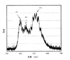
- FIG. 4 is a diagram showing the spectral characteristics of the light emitted from the light emitting element 30.
- the horizontal axis indicates the wavelength
- the vertical axis indicates the emission intensity.
- the light emitting element 30 emits light having three peaks and high intensity over almost the entire visible range.
- the peak P1 at a position of about 450 nm on the shortest wavelength side is due to the emitted light from the third light emitting layer 33A.
- peaks P2 and P3 located around 500 nm and 570 nm, respectively are due to the emitted light from the first and second light emitting layers 13A and 13B, respectively.
- it did not have the 3rd light emitting layer 33A, ie, in the light emitting element 10 it confirmed that it showed the spectral characteristic similar to the light emitting element 30 except having no peak P1.
- the case where two light emitting layers having island-shaped base segments are stacked has been described.
- the electron blocking layer 14 is formed between the light emitting functional layer 13 (or 33) and the p-type semiconductor layer 15 has been described.
- the present embodiment is limited to the case where the electron blocking layer 14 is provided. It is not a thing.
- the p-type semiconductor layer 15 may be formed on the light emitting functional layer 13.
- the electron block layer 14 has a larger band gap than the n-type semiconductor layer 12, the light emitting functional layer 13, and the p-type semiconductor layer 15. Therefore, it is possible to suppress the electrons from overflowing to the p-type semiconductor layer 15 side beyond the light emitting functional layer 13. Therefore, it is preferable to provide the electronic block layer 14 at the time of high current driving and at the time of high temperature operation.
- the first base segment BS1 in the first light emitting layer 13A and the second base segment BS2 in the second light emitting layer 13B are randomly formed independently of each other. Accordingly, the respective light emitting regions are different, and the light emitted in an overlapping manner has a wide light emission wavelength band. Furthermore, the first base layer BL1 and the second base layer BL2 have different average sizes of segments, so that the emitted light from the first and second light-emitting layers 13A and 13B can be made different (the wavelength band is changed). Can be shifted). Further, by configuring the first and second base layers BL1 and BL2 to have different layer thicknesses, the spectral widths of the emitted light from the first and second light emitting layers 13A and 13B are different.
- the light emitting functional layer 13 has a structure in which a plurality of light emitting layers including the first and second light emitting layers 13A and 13B are stacked.
- the first light-emitting layer 13A includes a first base layer BL1 having a plurality of first base segments BS1 having a composition that receives stress strain from the n-type semiconductor layer 12 and partitioned in a random network,
- the first quantum well layer WA formed on the first base layer BL1 while the segment shape of one base segment BS1 remains, and the first base layer BL1 and the first quantum well layer WA are embedded and flattened.
- a first barrier layer BA having a flattened flat surface FS1.
- the second light-emitting layer 13B has a composition that receives stress strain from the first barrier layer BA, and has a plurality of second base segments BS2 that are partitioned in a random network shape. And the second quantum well layer WB formed on the second base layer BL2 while the segment shape of the second base segment BS2 remains, and the second quantum well layer WB formed on the second quantum well layer WB. And a barrier layer BB. Therefore, it is possible to provide a light-emitting element that can emit light having high emission intensity over a wide visible range.
- the first conductivity type is the n-type conductivity type and the second conductivity type is the p-type conductivity type opposite to the n-type has been described.
- the conductivity type may be p-type, and the second conductivity type may be n-type.
Landscapes
- Chemical & Material Sciences (AREA)
- Inorganic Chemistry (AREA)
- Engineering & Computer Science (AREA)
- Materials Engineering (AREA)
- Led Devices (AREA)
Abstract
Description
[変形例]
図3は、実施例1の変形例に係る半導体発光素子30の構造を示す断面図である。発光素子30は、発光機能層33の構造を除いては、発光素子10と同様の構成を有している。発光素子30の発光機能層33は、n型半導体層12と発光素子10における第1の発光層13Aとの間に、少なくとも1つの第3の量子井戸層WCと複数の第3の障壁層WCとからなる量子井戸構造を有する第3の発光層33Aを有している。
12 n型半導体層(第1の半導体層)
13、33 発光機能層
13A 第1の発光層
13B 第2の発光層
33A 第3の発光層
14 電子ブロック層
15 p型半導体層(第2の半導体層)
BL1 第1のベース層
BS1 第1のベースセグメント
BL2 第2のベース層
BS2 第2のベースセグメント
GR1~GR4 第1~第4の溝
FS1 第1の平坦面
FS2 第2の平坦面
Claims (7)
- 第1の導電型を有する第1の半導体層と、前記第1の半導体層上に形成され、第1及び第2の発光層を含む発光機能層と、前記発光機能層上に形成され、前記第1の半導体層とは反対の導電型を有する第2の半導体層とを有する半導体発光素子であって、
前記第1の発光層は、前記第1の半導体層から応力歪を受ける組成を有してランダムな網目状に区画された複数の第1のベースセグメントを有する第1のベース層と、前記第1のベースセグメントのセグメント形状を残存しつつ前記第1のベース層上に形成された第1の量子井戸層と、前記第1のベース層及び前記第1の量子井戸層を埋め込んで平坦化された平坦面を有する第1の障壁層と、を有し、
前記第2の発光層は、前記第1の障壁層から応力歪を受ける組成を有してランダムな網目状に区画された複数の第2のベースセグメントを有する第2のベース層と、前記第2のベースセグメントのセグメント形状を残存しつつ前記第2のベース層上に形成された第2の量子井戸層と、前記第2の量子井戸層上に形成された第2の障壁層と、を有することを特徴とする半導体発光素子。 - 前記第1及び第2のベース層は、互いに異なる層厚を有していることを特徴とする請求項1に記載の半導体発光素子。
- 前記複数の第2のベースセグメントは、前記第2のベース層の面内において、前記第1のベース層の面内における前記複数の第1のベースセグメントとは異なる平均サイズを有していることを特徴とする請求項1又は2に記載の半導体発光素子。
- 前記第1の半導体層はGaNの組成を有し、
前記第1及び第2のベース層の各々はAlN又はAlGaNの組成を有し、
前記第1及び第2の量子井戸層の各々はInGaNの組成を有することを特徴とする請求項1乃至3のいずれか1つに記載の半導体発光素子。 - 前記第1及び第2のベース層は互いに異なるAl組成を有することを特徴とする請求項4に記載の半導体発光素子。
- 前記第1の障壁層は、前記第1の井戸層上に形成され、前記第1の井戸層よりも小さなIn組成を有するInGaNからなる第1の副障壁層と、前記第1の副障壁層上に設けられたGaNからなる第2の副障壁層とからなり、
前記第2の副障壁層は前記平坦面を有することを特徴とする請求項4又は5に記載の半導体発光素子。 - 前記発光機能層は、前記第1の半導体層と前記第1の発光層との間に、少なくとも1つの第3の量子井戸層と複数の第3の障壁層とを有する第3の発光層を有し、
前記複数の第3の障壁層のうち、最も第1の発光層側に位置する第3の障壁層は、前記第1の半導体層と同一の組成を有することを特徴とする請求項1乃至6のいずれか1つに記載の半導体発光素子。
Priority Applications (4)
| Application Number | Priority Date | Filing Date | Title |
|---|---|---|---|
| US15/525,056 US10186671B2 (en) | 2014-11-07 | 2015-10-22 | Semiconductor light-emitting element |
| KR1020177012267A KR102397661B1 (ko) | 2014-11-07 | 2015-10-22 | 반도체 발광 소자 |
| CN201580061116.9A CN107112391B (zh) | 2014-11-07 | 2015-10-22 | 半导体发光元件 |
| EP15857240.4A EP3217439B1 (en) | 2014-11-07 | 2015-10-22 | Semiconductor light-emitting element |
Applications Claiming Priority (2)
| Application Number | Priority Date | Filing Date | Title |
|---|---|---|---|
| JP2014226915A JP6433247B2 (ja) | 2014-11-07 | 2014-11-07 | 半導体発光素子 |
| JP2014-226915 | 2014-11-07 |
Publications (1)
| Publication Number | Publication Date |
|---|---|
| WO2016072276A1 true WO2016072276A1 (ja) | 2016-05-12 |
Family
ID=55909003
Family Applications (1)
| Application Number | Title | Priority Date | Filing Date |
|---|---|---|---|
| PCT/JP2015/079805 Ceased WO2016072276A1 (ja) | 2014-11-07 | 2015-10-22 | 半導体発光素子 |
Country Status (6)
| Country | Link |
|---|---|
| US (1) | US10186671B2 (ja) |
| EP (1) | EP3217439B1 (ja) |
| JP (1) | JP6433247B2 (ja) |
| KR (1) | KR102397661B1 (ja) |
| CN (1) | CN107112391B (ja) |
| WO (1) | WO2016072276A1 (ja) |
Cited By (2)
| Publication number | Priority date | Publication date | Assignee | Title |
|---|---|---|---|---|
| WO2016152473A1 (ja) * | 2015-03-23 | 2016-09-29 | スタンレー電気株式会社 | 半導体発光素子 |
| WO2016152842A1 (ja) * | 2015-03-23 | 2016-09-29 | スタンレー電気株式会社 | 半導体発光素子 |
Families Citing this family (7)
| Publication number | Priority date | Publication date | Assignee | Title |
|---|---|---|---|---|
| JP6433246B2 (ja) * | 2014-11-07 | 2018-12-05 | スタンレー電気株式会社 | 半導体発光素子 |
| KR102569461B1 (ko) * | 2015-11-30 | 2023-09-04 | 쑤저우 레킨 세미컨덕터 컴퍼니 리미티드 | 발광소자 및 이를 포함하는 조명장치 |
| JP2017220586A (ja) * | 2016-06-08 | 2017-12-14 | 国立大学法人 東京大学 | 半導体発光素子 |
| EP3796401B1 (en) * | 2018-05-18 | 2025-11-05 | Xiamen San'an Optoelectronics Co., Ltd. | Light-emitting diode epitaxial wafer |
| JP7595299B2 (ja) * | 2021-02-26 | 2024-12-06 | セイコーエプソン株式会社 | 発光装置およびプロジェクター |
| CN116344598A (zh) * | 2021-12-23 | 2023-06-27 | 无锡晶湛半导体有限公司 | 半导体结构及其制备方法 |
| CN116454186A (zh) * | 2023-06-15 | 2023-07-18 | 江西兆驰半导体有限公司 | 发光二极管外延片及其制备方法、发光二极管 |
Citations (4)
| Publication number | Priority date | Publication date | Assignee | Title |
|---|---|---|---|---|
| JP2005093682A (ja) * | 2003-09-17 | 2005-04-07 | Toyoda Gosei Co Ltd | GaN系半導体発光素子及びその製造方法 |
| JP2008053608A (ja) * | 2006-08-28 | 2008-03-06 | Stanley Electric Co Ltd | 窒化物半導体結晶ないしそれを用いた発光素子及びその製造方法 |
| JP2008199016A (ja) * | 2007-02-09 | 2008-08-28 | Koga Koden Kofun Yugenkoshi | 発光素子のエピタキシャル構造 |
| JP2009124149A (ja) * | 2007-11-14 | 2009-06-04 | Advanced Optoelectronic Technology Inc | Iii族元素窒化物半導体発光デバイス及びその作成方法 |
Family Cites Families (26)
| Publication number | Priority date | Publication date | Assignee | Title |
|---|---|---|---|---|
| US6608330B1 (en) * | 1998-09-21 | 2003-08-19 | Nichia Corporation | Light emitting device |
| JP4047150B2 (ja) | 2002-11-28 | 2008-02-13 | ローム株式会社 | 半導体発光素子 |
| US20070145386A1 (en) | 2004-12-08 | 2007-06-28 | Samsung Electro-Mechanics Co., Ltd. | Semiconductor light emitting device and method of manufacturing the same |
| TWI247439B (en) * | 2004-12-17 | 2006-01-11 | Genesis Photonics Inc | Light-emitting diode device |
| KR100691177B1 (ko) | 2005-05-31 | 2007-03-09 | 삼성전기주식회사 | 백색 발광소자 |
| JP2008071805A (ja) | 2006-09-12 | 2008-03-27 | Institute Of National Colleges Of Technology Japan | 複数種の蛍光体を2種類以上の半導体発光素子上に塗布した多波長発光装置。 |
| WO2008060594A2 (en) | 2006-11-15 | 2008-05-22 | The Regents Of The University Of California | High light extraction efficiency light emitting diode (led) through multiple extractors |
| KR100809229B1 (ko) * | 2006-11-20 | 2008-03-05 | 삼성전기주식회사 | 질화물 반도체 발광 소자 및 제조방법 |
| JP5050574B2 (ja) * | 2007-03-05 | 2012-10-17 | 住友電気工業株式会社 | Iii族窒化物系半導体発光素子 |
| KR101164026B1 (ko) | 2007-07-12 | 2012-07-18 | 삼성전자주식회사 | 질화물계 반도체 발광소자 및 그 제조방법 |
| KR101521259B1 (ko) | 2008-12-23 | 2015-05-18 | 삼성전자주식회사 | 질화물 반도체 발광소자 및 그 제조방법 |
| JP5354622B2 (ja) * | 2009-02-18 | 2013-11-27 | 独立行政法人産業技術総合研究所 | 半導体発光ダイオード |
| JP2010232597A (ja) | 2009-03-30 | 2010-10-14 | Toyoda Gosei Co Ltd | Iii族窒化物系化合物半導体発光素子及びその製造方法 |
| WO2011027417A1 (ja) * | 2009-09-01 | 2011-03-10 | 株式会社 東芝 | 半導体発光素子 |
| JP2011249460A (ja) | 2010-05-25 | 2011-12-08 | Meijo University | 白色発光ダイオード |
| CN103190005A (zh) | 2010-11-04 | 2013-07-03 | 皇家飞利浦电子股份有限公司 | 基于结晶弛豫结构的固态发光器件 |
| JP2012169383A (ja) | 2011-02-11 | 2012-09-06 | Toyoda Gosei Co Ltd | Iii族窒化物半導体発光素子およびその製造方法 |
| JP6155478B2 (ja) | 2012-01-31 | 2017-07-05 | ソイテックSoitec | 電荷キャリアの分布が改善された光活性デバイス及びその形成方法 |
| KR20130106690A (ko) | 2012-03-20 | 2013-09-30 | 삼성전자주식회사 | 백색 발광 다이오드 |
| WO2013174300A1 (en) | 2012-05-24 | 2013-11-28 | The University Of Hong Kong | White nanoled without requiring color conversion |
| US9024292B2 (en) * | 2012-06-02 | 2015-05-05 | Xiaohang Li | Monolithic semiconductor light emitting devices and methods of making the same |
| WO2014171048A1 (ja) | 2013-04-16 | 2014-10-23 | パナソニック株式会社 | 炭化珪素半導体装置およびその製造方法 |
| CN103746052B (zh) * | 2013-12-27 | 2016-08-17 | 太原理工大学 | 一种InGaN基多量子阱结构及其制备方法 |
| KR102212561B1 (ko) | 2014-08-11 | 2021-02-08 | 삼성전자주식회사 | 반도체 발광 소자 및 반도체 발광 소자 패키지 |
| JP6457784B2 (ja) | 2014-11-07 | 2019-01-23 | スタンレー電気株式会社 | 半導体発光素子 |
| CN105355741B (zh) | 2015-11-02 | 2017-09-29 | 厦门市三安光电科技有限公司 | 一种led外延结构及制作方法 |
-
2014
- 2014-11-07 JP JP2014226915A patent/JP6433247B2/ja not_active Expired - Fee Related
-
2015
- 2015-10-22 EP EP15857240.4A patent/EP3217439B1/en active Active
- 2015-10-22 US US15/525,056 patent/US10186671B2/en active Active
- 2015-10-22 CN CN201580061116.9A patent/CN107112391B/zh not_active Expired - Fee Related
- 2015-10-22 KR KR1020177012267A patent/KR102397661B1/ko active Active
- 2015-10-22 WO PCT/JP2015/079805 patent/WO2016072276A1/ja not_active Ceased
Patent Citations (4)
| Publication number | Priority date | Publication date | Assignee | Title |
|---|---|---|---|---|
| JP2005093682A (ja) * | 2003-09-17 | 2005-04-07 | Toyoda Gosei Co Ltd | GaN系半導体発光素子及びその製造方法 |
| JP2008053608A (ja) * | 2006-08-28 | 2008-03-06 | Stanley Electric Co Ltd | 窒化物半導体結晶ないしそれを用いた発光素子及びその製造方法 |
| JP2008199016A (ja) * | 2007-02-09 | 2008-08-28 | Koga Koden Kofun Yugenkoshi | 発光素子のエピタキシャル構造 |
| JP2009124149A (ja) * | 2007-11-14 | 2009-06-04 | Advanced Optoelectronic Technology Inc | Iii族元素窒化物半導体発光デバイス及びその作成方法 |
Non-Patent Citations (1)
| Title |
|---|
| See also references of EP3217439A4 * |
Cited By (4)
| Publication number | Priority date | Publication date | Assignee | Title |
|---|---|---|---|---|
| WO2016152473A1 (ja) * | 2015-03-23 | 2016-09-29 | スタンレー電気株式会社 | 半導体発光素子 |
| WO2016152842A1 (ja) * | 2015-03-23 | 2016-09-29 | スタンレー電気株式会社 | 半導体発光素子 |
| US9972749B2 (en) | 2015-03-23 | 2018-05-15 | Stanley Electric Co., Ltd. | Semiconductor light-emitting element |
| US9991420B2 (en) | 2015-03-23 | 2018-06-05 | Stanley Electric Co., Ltd. | Semiconductor light-emitting element |
Also Published As
| Publication number | Publication date |
|---|---|
| US20170324048A1 (en) | 2017-11-09 |
| JP2016092285A (ja) | 2016-05-23 |
| CN107112391A (zh) | 2017-08-29 |
| KR102397661B1 (ko) | 2022-05-13 |
| JP6433247B2 (ja) | 2018-12-05 |
| EP3217439B1 (en) | 2019-12-04 |
| EP3217439A4 (en) | 2018-06-06 |
| US10186671B2 (en) | 2019-01-22 |
| KR20170084066A (ko) | 2017-07-19 |
| CN107112391B (zh) | 2019-11-22 |
| EP3217439A1 (en) | 2017-09-13 |
Similar Documents
| Publication | Publication Date | Title |
|---|---|---|
| JP6433247B2 (ja) | 半導体発光素子 | |
| JP6433246B2 (ja) | 半導体発光素子 | |
| JP6457784B2 (ja) | 半導体発光素子 | |
| JP6605213B2 (ja) | 半導体発光素子 | |
| JP6433248B2 (ja) | 半導体発光素子 | |
| WO2016152772A1 (ja) | 半導体発光素子及びその製造方法 | |
| JP2017220586A (ja) | 半導体発光素子 | |
| JP6605214B2 (ja) | 半導体発光素子 | |
| JP6552234B2 (ja) | 半導体発光素子 | |
| JP2016178267A (ja) | 半導体発光素子 | |
| JP2017126684A (ja) | 半導体発光素子 |
Legal Events
| Date | Code | Title | Description |
|---|---|---|---|
| 121 | Ep: the epo has been informed by wipo that ep was designated in this application |
Ref document number: 15857240 Country of ref document: EP Kind code of ref document: A1 |
|
| REEP | Request for entry into the european phase |
Ref document number: 2015857240 Country of ref document: EP |
|
| ENP | Entry into the national phase |
Ref document number: 20177012267 Country of ref document: KR Kind code of ref document: A |
|
| WWE | Wipo information: entry into national phase |
Ref document number: 15525056 Country of ref document: US |
|
| NENP | Non-entry into the national phase |
Ref country code: DE |