WO2016076595A1 - 도파관 슬롯 어레이 안테나 - Google Patents
도파관 슬롯 어레이 안테나 Download PDFInfo
- Publication number
- WO2016076595A1 WO2016076595A1 PCT/KR2015/012036 KR2015012036W WO2016076595A1 WO 2016076595 A1 WO2016076595 A1 WO 2016076595A1 KR 2015012036 W KR2015012036 W KR 2015012036W WO 2016076595 A1 WO2016076595 A1 WO 2016076595A1
- Authority
- WO
- WIPO (PCT)
- Prior art keywords
- slot
- plate
- radiating plate
- polarization
- excitation
- Prior art date
- Legal status (The legal status is an assumption and is not a legal conclusion. Google has not performed a legal analysis and makes no representation as to the accuracy of the status listed.)
- Ceased
Links
Images




Classifications
-
- H—ELECTRICITY
- H01—ELECTRIC ELEMENTS
- H01Q—ANTENNAS, i.e. RADIO AERIALS
- H01Q13/00—Waveguide horns or mouths; Slot antennas; Leaky-waveguide antennas; Equivalent structures causing radiation along the transmission path of a guided wave
- H01Q13/10—Resonant slot antennas
-
- H—ELECTRICITY
- H01—ELECTRIC ELEMENTS
- H01Q—ANTENNAS, i.e. RADIO AERIALS
- H01Q21/00—Antenna arrays or systems
-
- H—ELECTRICITY
- H01—ELECTRIC ELEMENTS
- H01Q—ANTENNAS, i.e. RADIO AERIALS
- H01Q21/00—Antenna arrays or systems
- H01Q21/06—Arrays of individually energised antenna units similarly polarised and spaced apart
-
- H—ELECTRICITY
- H01—ELECTRIC ELEMENTS
- H01Q—ANTENNAS, i.e. RADIO AERIALS
- H01Q21/00—Antenna arrays or systems
- H01Q21/06—Arrays of individually energised antenna units similarly polarised and spaced apart
- H01Q21/20—Arrays of individually energised antenna units similarly polarised and spaced apart the units being spaced along or adjacent to a curvilinear path
Definitions
- the present invention relates to ultra-high frequency transmit and receive antennas, and more particularly to waveguide slot array antennas.
- Ultra-high frequency transceiver antennas include parabolic antennas, microstrip antennas and waveguide slot array antennas. Among these antennas, a microstrip array antenna or a waveguide slot array antenna is mainly used for miniaturization by reducing thickness.
- the microstrip array antenna has a microstrip patch array structure using a dielectric substrate, and according to the dielectric loss factor of the dielectric substrate, the loss of the signal transmitted or received is large, the resistance loss of the conductor occurs, and especially the frequency As the loss increases, the loss is avoided in the ultra-high frequency band.
- the waveguide slot array antenna has a structure in which a slot-shaped hole is formed in a general waveguide without using such a dielectric substrate.
- the waveguide is a hollow metal tube, a kind of highpass filter.
- the mode of the tube has a constant cutoff wavelength, and the basic mode is determined by the size of the waveguide.
- waveguides have the advantage of low attenuation compared to parallel two-wire lines or coaxial cables, and thus have been mainly used for high power in microwave transmission lines.
- the waveguide has various cross-sectional shapes, and is divided into a circular waveguide, a rectangular waveguide, an elliptical waveguide, and the like according to the cross-sectional shape.
- Korean patent application No. 2006-18147 name: “stacked slot array antenna”, Applicant: Monetix, Inventor: Cho Tae-gwan, etc., filed date: 2006 Feb. 24, 2013, or domestic patent application No. 2007-7000182 (name: “Planar antenna module, triple plate type flat array antenna and triple plate line-waveguide transducer”), Applicant: Hitachi Kasei Kogyo Co., Ltd. , Inventor: Ota Masahiko et al., Filing date: January 04, 2007).
- a conventional waveguide slot array antenna includes a feed plate 11 having an input feed slot 112 formed therein; A distribution plate 12 installed on the power feeding plate 11 and having a distribution portion and a coupling slot 122; A main radiating plate 13 installed on the distribution plate 12 and having a cavity structure and an excitation slot 132 (or a radiating slot) formed thereon; It is installed on the main radiating plate 13, it can be configured to include an auxiliary radiating plate 14 formed with a polarization slot 142 for generating a polarized inclination of 45 degrees polarized surface.
- the input signal When a signal is input from the feed slot 112 of the feed plate 11, the input signal is distributed through the distribution plate 12, for example, at an equal ratio, and the divided signals are respectively coupled to the coupling slot 122.
- the distribution plate 12 Through each of the cavities formed in the main radiating plate (13).
- the signal transmitted to the cavity of the main radiating plate 13 is distributed and radiated at the same rate through the excitation slots 132 which are formed for each of four cavities, for example.
- These excitation slots 132 are arranged to have a predetermined interval and arrangement between each other according to the operating frequency.
- polarization slots 142 are formed in a one-to-one correspondence with each excitation slot 132 of the main radiating plate 13, and a polarization is formed.
- the signal transmitted to the slot 142 is rotated by 45 degrees compared to the case where the polarization plane is emitted from the excitation slot 132 is radiated into the space. That is, the secondary radiating plate 14 generates 45 degree polarization relative to the vertical and horizontal.
- the slot shape of the excitation slot 142 is, for example, a substantially rectangular shape, it may be formed in an upright position based on the vertical / horizontal direction, the polarization slot 142
- the slot shape may have a rectangular shape similar to the slot shape of the approximately rectangular excitation slot 132, but the rectangular shape is mechanically rotated 45 degrees relative to the vertical / horizontal shape compared to the slot shape of the excitation slot 132. Having a structure formed in a posture, it can be formed similarly to a rhombus shape as a whole.
- This structure may be regarded as a structure in which one radiation slot is formed by the combination of the excitation slot 132 and the polarization slot 142.
- the auxiliary radiation plate 14 is used to operate the conventional waveguide slot array antenna with vertical / horizontal polarization, and the polarization slot 142 of the auxiliary radiation plate 14 is a signal radiated from the excitation slot 132. It may have a rectangular shape rotated 45 degrees relative to the excitation slot 132 to rotate the polarization plane of 45 degrees.
- This structure has the advantage that the side lobe component is significantly suppressed by the total length of the horizontal and vertical surfaces.
- the rectangular polarization slot 142 formed in the auxiliary radiating plate 14 is formed in a shape rotated 45 degrees from the vertical / horizontal plane to have a shape similar to a rhombus shape, the polarization slot in the vertical / horizontal plane ( The spacing between arrays 142 does not meet the appropriate distance criteria required when considering the wavelength of the operating frequency. That is, as indicated by the interval 'a' in FIG. 1A, in particular, a distance between the polarization slots 142 positioned diagonally from each other increases. Such a structure can generate a grating lobe.
- a constant radiation angle at which the phase of the emitted signal in each radiation slot is the same is generated.
- the lobe that occurs at this time is called a grating lobe and is a kind of main lobe.
- the grating lobe is generated by the phase of the array element in the array antenna, whose phase is governed by the distance between the elements.
- FIG. 1B shows the generation state of the main lobe and the grating lobe at positions P1 and P2 of two polarization slots diagonally positioned (distance d) in FIG. 1A, for example.
- a grating lobe occurs when the difference between the main lobe and the phase of the two paths at a rotation angle by ⁇ therefrom is one wavelength ⁇ .
- the generated angle can be simply expressed by the following equation.
- the grating lobe Due to the grating lobe, the grating lobe does not satisfy the limitation of the Radiation Pattern Envelope (RPE) standard. Therefore, there is a need for a way to suppress such grating lobes.
- RPE Radiation Pattern Envelope
- the excitation slots are arranged to have a large number of excitation slots arranged in the same antenna area, it is possible to consider a method of suppressing the grating lobe, but in the conventional structure, depending on the cavity structure in which signals are distributed in the distribution plate and the main radiating plate. Since the number of excitation slots is increased by a power of two, there are limitations in the layout design of the excitation slots.
- the present invention has been proposed to solve the above problems, and to provide a waveguide slot array antenna for generating a polarization while suppressing the grating lobe more effectively.
- Another object of the present invention is to provide a waveguide slot array antenna for increasing the degree of freedom in designing a slot array so that the overall antenna structure can be more freely implemented.
- a waveguide slot array antenna having an excitation slot array for emitting a signal corresponding to an operating frequency in the main radiating plate;
- a first auxiliary radiating plate installed on the main radiating plate, the first auxiliary radiating plate rotating a polarization plane of a signal radiated in an excitation slot arrangement of the main radiating plate; It is installed on the first auxiliary radiating plate, characterized in that it comprises a second auxiliary radiating plate for distributing and radiating a signal whose polarization surface is rotated in the first auxiliary radiating plate.
- the first auxiliary radiating plate is formed with an array of first polarization slots formed in a structure corresponding to the excitation slot arrangement of the main radiating plate;
- the first polarization slot may have a structure for rotating the polarization plane of the signal radiated from the corresponding excitation slot.
- the second auxiliary radiating plate has an arrangement of a plurality of second polarization slots corresponding to each of the first polarization slots of the first auxiliary radiating plate;
- a distribution structure may be formed for distributing signals radiated for each of the first polarization slots of the first auxiliary radiating plate to a plurality of corresponding second polarization slots.
- a feed plate forming at least a portion of the waveguide for receiving an input signal; And a distribution plate having a distribution waveguide structure coupled to the feeder plate for distributing the input signal to a plurality of coupling slots, wherein the main radiating plate is installed on the distribution plate, each couple of distribution plates.
- a plurality of cavity structures may be provided for distributing the signals input through the ring slots at the same ratio and for exciting the divided signals through the excitation slot arrangement.
- a waveguide slot array antenna A distribution plate having a distribution waveguide structure for distributing an input signal to the plurality of coupling slots; A plurality of coupling slots installed on the distribution plate for distributing the signals input through the plurality of coupling slots of the distribution plate at the same rate and for exciting the distributed signals through a plurality of excitation slot arrangements, respectively.
- a radiation plate having a plurality of cavity structures configured correspondingly thereto; Each of the plurality of cavity structures is designed to be divided into four areas for distributing signals provided to corresponding coupling slots of the distribution plate into four parts, and a plurality of excitation slots are formed in each of the four areas. It is done.
- the waveguide slot array antenna can generate a polarization while suppressing the grating lobe more effectively, thereby reducing the influence on the adjacent equipment in the adjacent fixed communication device.
- the waveguide slot array antenna can increase the degree of freedom in designing the slot array, so that the overall antenna structure can be more freely implemented. As a result, unnecessary antenna size increase can be prevented, and the proper alignment level can be maintained to reduce the processing complexity, thereby reducing the cost of time.
- 1A is a partially cut away perspective view of each layer of a conventional exemplary waveguide slot array antenna
- FIG. 1B is an exemplary view showing a grating lobe generation state in the waveguide slot array antenna of FIG. 1A
- FIG. 2 is a partially cut perspective view of each layer of the waveguide slot array antenna according to the first embodiment of the present invention.
- FIG. 3 is a perspective view of one side of the second auxiliary radiating plate of FIG.
- FIG. 4 is another perspective view of the second auxiliary radiating plate of FIG. 2;
- FIG. 5 is a perspective view illustrating a connection relationship between a second polarization slot of a second auxiliary radiation plate and a first polarization slot of a first auxiliary radiation plate in FIG. 2.
- FIG. 6 is a side structure diagram illustrating a connection relationship between a second polarization slot of a second auxiliary radiation plate and a first polarization slot of a first auxiliary radiation plate in FIG. 2;
- FIG. 7 is a side view illustrating a connection relationship according to a modified structure of a second polarization slot of a second auxiliary radiating plate and a first polarization slot of a first auxiliary radiating plate in FIG.
- FIG. 8 is a perspective view of one side of the first auxiliary radiating plate of FIG. 2; FIG.
- FIG. 9 is a perspective view of one side direction of the radiating plate of FIG.
- FIG. 10 is a perspective view of the other side of the radiation plate in FIG.
- FIG. 11 is a perspective view of one side direction of the distribution plate of FIG. 2; FIG.
- FIG. 12 is a perspective view of the other side of the distribution plate in FIG.
- FIG. 13 is a plan view of the feeder plate of FIG. 2.
- FIG. 14 is a structural diagram of an internal signal waveguide path of the waveguide slot array antenna according to the first embodiment of the present invention.
- 15 is a graph illustrating grating lobe characteristics of the waveguide slot array antenna of FIG. 14.
- 16 is a graph illustrating cross polarization characteristics of the waveguide slot array antenna of FIG. 14.
- 17 is a perspective view of an essential part of a waveguide slot array antenna for comparison with embodiments of the present invention.
- FIG. 18 is a structural diagram of an internal signal waveguide path of the waveguide slot array antenna of FIG. 17.
- FIG. 19 is a perspective view of an essential part of a waveguide slot array antenna according to a second embodiment of the present invention.
- 20 is a structural diagram of an internal signal waveguide path of the waveguide slot array antenna of FIG.
- 21 is a perspective view of an essential part of a waveguide slot array antenna according to a third embodiment of the present invention.
- FIG. 22 is a structural diagram of an internal signal waveguide path of the waveguide slot array antenna of FIG. 21.
- Figure 23 is an exploded perspective view of one side view of the main part of the waveguide slot array antenna according to the fourth embodiment of the present invention.
- FIG. 24 is an exploded perspective view of the other side of the waveguide slot array antenna of FIG. 23.
- FIG. 25 is a perspective view of one side view of the radiating plate of FIG. 23; FIG.
- FIG. 26 is a perspective view of the other side of the radiation plate in FIG.
- FIG. 27 is a perspective view of one side view of the distribution plate of FIG. 23; FIG.
- FIG. 28 is a perspective view of the other side of the distribution plate in FIG.
- 29 is a perspective view of an essential part of a waveguide slot array antenna according to a fifth embodiment of the present invention.
- FIG. 30 is a perspective view of an essential part of a waveguide slot array antenna according to a sixth embodiment of the present invention.
- the waveguide slot array antenna according to the first embodiment of the present invention may include a feed plate 11 having an input feed slot 112, similar to the conventional art; A distribution plate 12 installed on the power feeding plate 11 and having a distribution portion and a coupling slot 122; The main radiating plate 13 may be basically provided on the distribution plate 12 and provided with a cavity structure and an excitation slot 132 (or a spinning slot).
- the first auxiliary radiating plate (installed on the main radiating plate 13, the first auxiliary radiating plate (142) having a first polarization slot 142 for generating a polarization inclined 45 degrees polarization plane ( 14); And a second auxiliary radiating plate 15 provided on the first auxiliary radiating plate 14 and having a second polarization slot 152 for distributing and radiating the polarization generated by the first auxiliary radiating plate 14. Equipped.
- each distributed signal is mainly transmitted through the coupling slots 122. It is delivered to each cavity formed in the radiation plate 13.
- the signal transmitted to the cavity of the main radiating plate 13 is distributed and radiated in an equal ratio, for example, through the excitation slots 132 formed for each of four cavities, for example.
- These excitation slots 132 are arranged to have a predetermined interval and arrangement between each other according to the operating frequency.
- the first auxiliary radiating plate 14 provided on the main radiating plate 13 has a first polarization slot in a structure corresponding to one-to-one correspondence with each of the excitation slots 132 of the main radiating plate 13 as in the related art. 142 are formed.
- the first polarization slot 142 has a structure in which an approximately (rectangular) rectangular slot is mechanically rotated by 45 degrees relative to the excitation slot 132.
- the signal transmitted to the first polarization slot 142 through this structure generates a polarization signal that is rotated by 45 degrees compared to the case where the polarization plane is radiated from the excitation slot 132.
- each of the first polarization slots of the first auxiliary radiation plate 14 may be provided in the second auxiliary radiation plate 15 installed on the first auxiliary radiation plate 14.
- Each of the second polarization slots 152 formed to correspond to the plurality of second polarization slots 152 and the plurality of second polarization slots 152 corresponding to each of the first polarization slots 142.
- a dispensing structure for dispensing is formed. The shape (and posture) of the first polarization slot 142 and the plurality of second polarization slots 152 may be the same. Through this structure, the second polarization slots 152 are distributed and radiated through the second polarization slot 152 generated in the first polarization slot 142.
- the first auxiliary radiating plate 14 and the second auxiliary radiating plate 15 generally have a structure for rotating the signal excited from the excitation slot 132 of the main radiating plate 13 so that the polarization plane is inclined at 45 degrees. It can be seen that the additional slot array structure using the electric field or the magnetic field signal distribution structure is additionally formed.
- FIG. 3 is a perspective view of an upper side of the second auxiliary radiating plate 15 (eg, the front side based on the signal emission direction), and FIG. 4 is a lower side of the second auxiliary radiating plate 15 (eg, signal radiation).
- 5 and 6 are views of the second polarization slot 152 of the second auxiliary radiating plate 15 and the first polarization slot 142 of the first auxiliary radiating plate 14.
- a perspective view and a side view showing a connection relationship. 3 to 6, the configuration and operation of the second auxiliary radiating plate 15 and the second polarization slot 152 will be described in more detail.
- the signal transmitted from the excitation slot 132 of the main radiating plate 13 will be described.
- the electric field of is fixed after 45 degrees rotation in the first polarization slot 142 of the first auxiliary radiating plate 14 is transmitted to the second polarization slot 152 side of the second auxiliary radiating plate 15.
- the signal transmitted to the second auxiliary radiating plate 15 is distributed through a distribution structure formed under the second polarization slots 152 and is provided to the plurality of second polarization slots 152, respectively.
- This distribution structure may have a distribution structure that branches in the vertical or horizontal direction to the electric field plane.
- the signal distributed and provided to the second polarization slot 152 may be radiated into a space, and may be represented by the radiation pattern of the entire antenna.
- the arrangement interval of the second polarization slots 152 is the arrangement interval of the first polarization slots 152 of the first auxiliary radiating plate 14 according to the branched surface. In comparison, for example, they may be arranged at half intervals. That is, by this structure, the arrangement interval in the vertical / horizontal plane of the second polarization slot 152 formed in the second auxiliary radiating plate 15 can satisfactorily satisfy within one wavelength of the operating frequency, and the grating lobe Is sufficiently suppressed.
- FIG. 7 illustrates a modified structure of the second polarization slot 152 of the second auxiliary radiating plate 15 and the first polarization slot 142 of the first auxiliary radiating plate 14 in FIG. 2.
- the second auxiliary radiating plate 15 is similarly formed with the second polarization slot 152-1, but the distribution structure is not formed under the second polarization slot 152.
- This distribution structure is formed on the upper side of the first polarization slot 142-1 of the first auxiliary radiating plate 14. That is, in the modified structure shown in FIG. 7, only the second polarization slot 152-1 is formed in the second auxiliary radiation plate 15, and the first auxiliary radiation plate 14 is the first polarization slot 142-1. ) And a distribution structure formed on the upper side thereof.
- the first auxiliary radiating plate 14 and the second auxiliary radiating plate 15 are coupled to each other, the first auxiliary radiating plate 14 and the second auxiliary radiating plate 15 are formed by the first polarization slot 142-1, the distribution structure, and the second polarization slot 152-1.
- the shape of the waveguide path through which the internal signal is transmitted is substantially the same as that of the waveguide path formed by the structure shown in FIGS. 2 to 6, and the signal transmission characteristics are the same.
- FIG. 8 is a perspective view of one side of the first auxiliary radiating plate 14 of FIG. 2
- FIG. 9 is a perspective view of an upper side of the radiating plate 13 of FIG. 2 (eg, a front side based on a signal emission direction).
- 10 is a perspective view of the lower side of the radiation plate 13 in FIG. 2 (for example, a rear side based on a signal emission direction)
- FIGS. 11 and 12 are perspective views of the upper side and one side of the distribution plate 12 in FIG.
- FIG. 13 is a plan view of the feed plate 11 in FIG. 2.
- 8 to 12 the basic configuration and operation of the waveguide slot array antenna will be described in more detail. 8 to 12 are shown in the order in which the plates are installed on the lower side, the following description will be described based on the signal input and the waveguide path.
- a waveguide for guiding a signal input through an input connector (not shown) may be formed in an appropriate shape on one side based on the bottom surface of the feed plate 11.
- the bottom surface of the feed plate 11 may be formed, for example, from several millimeters to ten millimeters or less.
- the feed slot 112 is formed at the end of the waveguide of the feed plate 11, the feed slot 112 is composed of a plurality of stages to achieve matching according to the size of the distribution waveguide formed in the corresponding distribution plate 12. May be
- the back of the feed plate 11 may be machined holes or tabs corresponding to the fastening portion of the normalized waveguide flange.
- the distribution plate 12 connected to the feed plate 11 has a distribution waveguide structure for distributing a signal input through the feed slot 112 of the feed plate 11 to the plurality of coupling slots 122. .
- the number of the last branched branches of this distribution waveguide structure has a structure distributed by the number of squares of 2, and has a vertical symmetry structure.
- Such a distribution waveguide structure may have an electric field or a magnetic field distribution structure.
- the electric field or the magnetic field distribution structure may further have an iris and septum structure in consideration of matching characteristics.
- Coupling slots 122 are formed at the ends of each branched final branch in the distribution waveguide structure.
- the coupling slot 122 is offset from the center of the waveguide structure at the ends of the final branches of the distribution waveguide structure so as to be biased to one side to cause strong coupling.
- the main radiating plate 13 connected to the distribution plate 12 distributes the signals input through the coupling slots 122 of the distribution plate 12 at an equal or unequal ratio and distributes the distributed signals. It has a cavity structure for exciting through the excitation slot 132.
- Each coupling slot 122 of the distribution plate 12 is designed to be located in the center of each corresponding cavity of the main radiating plate 13.
- Each cavity may be configured such that, for example, four excitation slots 132 are formed.
- a partition wall having a predetermined length perpendicular to each side of the cavity may be formed. Is formed.
- the feed plate 11, the distribution plate 12, the main radiating plate 13 can be designed, corresponding to the first auxiliary radiating plate 14 and the second auxiliary radiating plate 15 is designed.
- the feed plate 11, the distribution plate 12, the main spin plate 13, the first subsidiary spin plate 14 and the second subsidiary spin plate 15 are aligned to each other and designed to be coupled to each other.
- the coupling method of each plate may be a screw fastening method, a soldering method or a high frequency welding method using a screw.
- FIG. 14 is a structural diagram of a part of an internal signal waveguide path of a waveguide slot array antenna according to a first embodiment of the present invention.
- the structure according to some embodiments of the present invention is illustrated in FIG. In Fig. 14A, for comparison, an internal signal waveguide path (or part thereof) corresponding to a conventional waveguide slot array antenna, as shown in Fig. 1, is shown.
- FIG. 15 is a graph illustrating grating lobe characteristics of the waveguide slot array antenna of FIG. 14, and
- FIG. 16 is a graph illustrating cross polarization characteristics of the waveguide slot array antenna of FIG. 14.
- a characteristic graph according to the first embodiment of the present invention is shown in (b), and FIG. 16 (a) corresponds to a conventional waveguide slot array antenna as shown in FIG. 1 for comparison.
- a characteristic graph is shown.
- the waveguide slotted array antenna according to the present invention can be regarded as a structure in which a second auxiliary radiating plate 15 is added, compared to the conventional one, and a single layer (plate) is physically The stacked structure, but the overall height of the antenna can be implemented as in the prior art. That is, as shown in Figure 14, the total height h1 of the conventional antenna and the total height h2 of the antenna according to the present invention can be designed to be the same. Even in this design, as shown in FIG. 15, the size of the primary and secondary side lobes is similar to the conventional one, but it can be seen that the grating lobe characteristic of the antenna according to the present invention is further improved.
- the determining factor of the cross polarization is dominantly determined by the height of the radiation slot at the end.
- the height h21 of the radiation slot (second polarization slot) at the last stage of the antenna according to the present invention is more than the height h11 of the radiation slot (first polarization slot) at the conventional antenna end stage. It can be seen that the design is low. This is a result of designing the overall height of the antenna according to the present invention as in the prior art, as shown in Figure 16, it can be seen that there is no deterioration of the cross-polarization characteristics even in such a design.
- the antenna according to the present invention can be seen that the cross-polarization characteristic is significantly improved.
- the present invention can be designed to optimize the height of the radiation slot of the last end of the antenna.
- FIG. 17 is a perspective view of an essential part of a waveguide slot array antenna for comparison with embodiments of the present invention
- FIG. 18 is a structural diagram of an internal signal waveguide path of the waveguide slot array antenna of FIG. 17.
- the waveguide slot array antenna shown in FIGS. 17 and 18 has a structure in which the feeder plate 21, the distribution plate 22, and the radiating plate 23 are stacked in this order as in the structure of the first embodiment shown in FIG. You can basically have
- auxiliary radiating plate (s) for polarization generation may be additionally installed on the radiating plate 23 similarly to the structure shown in FIG. 2.
- the structure shown in Figure 2, etc. discloses a structure in which an input signal is provided through the feed slot of the feed plate, for example, in Figure 17 and 18, for example, the signal input to one side of the distribution plate 22 It illustrates a structure in which an input signal is provided through a feed waveguide 212 in which an opening is formed for the purpose.
- the distribution plate 22 forms an empty area of the distribution waveguide structure for distributing the signal input through the feed waveguide 212 and the feed waveguide 212, and the feed plate 21 is simply a flat plate. It can be configured as.
- each of the divided signals is formed on the radiating plate 23. It is delivered to each cavity 230.
- the signal transmitted to the cavity 230 of the radiating plate 23 is distributed and radiated in an equal ratio through, for example, the excitation slots 232 formed by four, for example, for each cavity 230.
- These excitation slots 232 are arranged to have a predetermined interval and arrangement between each other according to the operating frequency.
- the input signal at the distribution plate 22 is distributed evenly, for example, in powers of two.
- the excitation slot 232 is a 2x2, 4x4 array, etc. They are arranged in powers.
- the radiating plate 22 illustrated in FIGS. 17 and 18 four signals input from one coupling slot of the distribution plate 22 and transmitted to one cavity of the radiating plate 23 are formed per cavity. Is configured to radiate through the excitation slot 232. Accordingly, it can be seen that the structure of the excitation slot 232 has a total arrangement of 4x4, 8x8, 16x16, and the like.
- the signal distribution structure generally uses a H-junction structure to implement a symmetrical and efficient feeder network structure.
- this structure due to this structure, there is a limitation of horizontal and vertical beam patterns, it is difficult to design a flexible gain and may have a volume more than necessary.
- the structure of the radiation plate shown in Figs. 17 and 18, the interval of the arrangement of the excitation slot can be narrower than the other embodiments shown in Fig. 2, etc., in some cases, shown in Fig.
- the grating lobe can be suppressed without providing a second auxiliary spin plate or the like above.
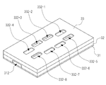
- FIG. 19 is a perspective view of an essential part of a waveguide slot array antenna according to a second embodiment of the present invention
- FIG. 20 is a structural diagram of an internal signal waveguide path of the waveguide slot array antenna of FIG. 19, wherein an excitation slot is a minimum arrangement unit (for example, 4x2) shows an example of a basic structure.
- an excitation slot is a minimum arrangement unit (for example, 4x2) shows an example of a basic structure.
- the waveguide slot array antenna according to the second embodiment of the present invention is similar to the structure shown in Figs.
- the feed plate 31 It is installed to be stacked on the feed plate 31, the waveguide structure for transmitting a signal input through the feed waveguide 312 and the feed waveguide 312 to the radiating plate 33 through a coupling slot (not shown)
- a distribution plate 32 having; It is installed to be stacked on the distribution plate 32, a plurality of excitation slots (332: 332-1, 332-2, 332-3, 332-4, 332-5, 332-6. 332-7, 332- And a radiation plate 33 having a cavity structure 330 for distributing the signal input through the coupling slot of the distribution plate 32 and exciting it through the excitation slots 332. It is composed.
- the auxiliary radiation plate (s) for polarization generation may be additionally installed on the radiation plate 33.
- the cavity structure 330 of the radiating plate 33 has four regions (a) for equally distributing the signal provided from the distribution plate 32 into four parts, for example. , b, c, and d), and thus, partition walls of a predetermined length are formed in each direction of the cavity in a vertical direction.
- two excitation slots are formed in the four areas a, b, c, and d of the cavity structure 330, unlike the structures shown in FIGS. 17 and 18.
- first and second excitation slots 332-1 and 332-2 are formed in the first region a in the cavity structure 330, and the first and second excitation slots 332-1 and 332 are formed.
- excitation slots 332-3 and 332-4 are formed in the second region b, and fifth and sixth excitation slots 332-5 and 332-are formed in the third region c. 6) is formed, and the seventh and eighth excitation slots 332-7 and 332-8 are formed in the fourth region d.
- the distribution plate 32 transmits the signal input through the feed waveguide 312 to the radiating plate 33 through one coupling slot as it is without distribution. It can be seen that the structure having. This is because the excitation slot arrangement structure shown in Figs. 19 and 20 is shown as having a minimum arrangement unit of, for example, 4x2 (width x length) for convenience of description. It will be appreciated that in the case of constructing such a minimum arrangement unit structure redundantly, the distribution plate 32 may have a configuration of distributing the input signal in the overlapping arrangement of the minimum arrangement unit structure.
- FIG. 21 is a perspective view of an essential part of a waveguide slot array antenna according to a third embodiment of the present invention
- FIG. 22 is a structural diagram of an internal signal waveguide path of the waveguide slot array antenna of FIG. 21, wherein an excitation slot is a minimum arrangement unit (for example, 6x2) shows an example of a basic structure.
- an excitation slot is a minimum arrangement unit (for example, 6x2) shows an example of a basic structure. 21 and 22, the waveguide slot array antenna according to the third embodiment of the present invention is similar to the structure according to the second embodiment shown in Figs.
- the feed plate 41 It is installed to be stacked on the feed plate 41, a waveguide structure for transmitting a signal input through the feed waveguide 412 and the feed waveguide 412 to the radiating plate 43 through a coupling slot (not shown)
- a distribution plate 42 having; It is installed to be stacked on the distribution plate 42, a plurality of excitation slots (432: 432-1, 432-2, 432-3, 432-4, 432-5, 432-6, 432-7, 432- 8, 432-9, 432-10, 432-11, and 432-12 are formed, and the signal inputted through the coupling slot of the distribution plate 42 is distributed to excite through the excitation slots 432.
- a radiation plate 43 having a cavity structure 430.
- auxiliary radiating plate (s) (not shown) for generating a polarization may be additionally installed.
- the cavity structure 430 of the radiating plate 43 is divided into four regions (a) for equally distributing the signal provided from the distribution plate 42 into four parts, for example. , b, c, and d), and thus, partition walls of a predetermined length are formed in each direction of the cavity in a vertical direction.
- three excitation slots are formed in the four areas a, b, c, and d of the cavity structure 430, unlike the structures shown in FIGS. 19 and 20. That is, in the cavity structure 430, first to third excitation slots 432-1, 432-2, and 432-3 are formed in the first region a, and the first to third excitation slots 432-1 are formed.
- fourth to sixth excitation slots 432-4, 432-5, and 432-6 are formed in the second region b, and seventh and ninth excitation slots 432- are formed in the third region c. 7, 432-8, and 432-9 are formed, and the tenth and twelfth excitation slots 432-10, 432-11, and 432-12 are formed in the fourth region d.
- the excitation slots of the radiating plate are arranged in comparison to the structure of a power of two, which is a general scheme. This will provide more flexibility in structural design.
- the overall antenna structure can implement the maximum directory at any size, and the overall thin structure can be maintained.
- FIG. 23 is an exploded perspective view of one side (eg, upper side) view of a main part of the waveguide slot array antenna according to the fourth embodiment of the present invention
- FIG. 24 is the other side (eg, of the waveguide slot array antenna of FIG. 23).
- 25 and 26 are perspective views of one side and the other side of the radiating plate 53 of FIG. 23, and
- FIGS. 27 and 28 are one side and the other side views of the distribution plate 52 of FIG. 23.
- the excitation slot has an arrangement structure of, for example, 10x4 (vertical x horizontal).
- the waveguide slot array antenna according to the fourth embodiment of the present invention, similar to the structure of the other embodiments, the feed plate 51; It is installed to be stacked on the feed plate 51, and the signal input through the feed waveguide 512 and the feed waveguide 512 is, for example, through a plurality of coupling slots 522 designed to be the square root of two.
- a distribution plate 52 having a distribution waveguide structure for distributing it evenly or evenly to the radiation plate 53; Cavity is installed on the distribution plate 52, excitation slots are formed, the cavity for distributing the signal input through the plurality of coupling slots 522 of the distribution plate 52 to excite through the excitation slots It is configured to include a spin plate 53 having a structure.
- auxiliary radiation plate (s) (not shown) for the generation of polarization may be additionally installed.
- the radiating plate 53 according to the fourth embodiment of the present invention is actually properly arranged and connected by using the structure of the radiating plate according to the previous other embodiments in duplicate It can be seen that it is a structure.
- the radiating plate 53 of the 10x4 arrangement actually has a 4x2 minimum array unit structure according to the second embodiment shown in FIGS. 19 and 20. It is applied to two places (for example, a 4x4 arrangement structure is formed), and the 6x2 minimum arrangement unit structure according to the third embodiment shown in FIGS. 21 and 22 is applied to two places of the b area and the d area. (Thus forming a 6x4 array structure, for example).
- the radiating plate 53 illustrated in FIG. 23 is implemented by applying a total of four minimum array unit structures, each having two minimum array unit structures according to the second and fourth embodiments.
- FIG. 29 is a perspective view of an essential part of a waveguide slot array antenna according to a fifth embodiment of the present invention, in which an excitation slot has an arrangement structure of, for example, 8x4 (vertical x horizontal).
- the waveguide slot array antenna according to the fifth embodiment of the present invention has a feed plate 61 similar to the structure of the fourth embodiment shown in FIGS. 23 to 28;
- the distribution plate 62 and the radiating plate 63 are laminated.
- the radiating plate 63 of the 8x4 array structure may be interconnected using four 4x2 minimum array unit structures according to the second embodiment shown in FIGS. 19 and 20. Can be.
- FIG. 30 is a perspective view of an essential part of a waveguide slot array antenna according to a sixth embodiment of the present invention, in which an excitation slot has an arrangement structure of, for example, 10x8 (vertical x horizontal).
- the waveguide slot array antenna according to the sixth embodiment of the present invention has a feed plate 71 similar to the structure of the fourth embodiment shown in FIGS. 23 to 28;
- the distribution plate 72 and the radiating plate 73 are laminated.
- the radiation plate 63 of the 10x8 arrangement shown in FIG. 30 has a 4x2 minimum arrangement unit structure according to the second embodiment shown in FIGS. 19 and 20, and the third shown in FIGS. 21 and 22.
- the 6x2 minimum array unit structure according to the embodiment and four of each can be implemented to be interconnected.
- the auxiliary radiating plate (s) of the present invention can also be applied to waveguide slot array antennas of various structures having a radiating slot arrangement. That is, in the waveguide slot array antenna having various structures, in order to generate polarization, as in the structure according to the first embodiment of the present invention, the first polarization slot and the second polarization slot are formed corresponding to the corresponding radiation slot arrangement. It may be possible to configure the first and second auxiliary radiating plate to be installed.
- the feed waveguide is formed on the distribution plate, but the structure in which the feed slot is formed on the feed plate is adopted in the same manner as the structure of the first embodiment. Of course you can.
Landscapes
- Variable-Direction Aerials And Aerial Arrays (AREA)
Abstract
Description
Claims (11)
- 주 방사판에서 동작주파수에 대응되는 신호를 방사하는 여기(excitation) 슬롯 배열을 갖는 도파관 슬롯 어레이 안테나에 있어서,상기 주 방사판 상에 설치되며, 상기 주 방사판의 여기슬롯 배열에서 방사되는 신호의 편파면을 회전시키는 제1보조 방사판과;상기 제1보조 방사판 상에 설치되며, 상기 제1보조 방사판에서 편파면이 회전된 신호를 분배하여 방사하는 제2보조 방사판을 포함함을 특징으로 하는 도파관 슬롯 어레이 안테나.
- 제1항에 있어서,상기 제1보조 방사판은, 상기 주 방사판의 상기 여기슬롯 배열과 대응되는 구조로 형성되는 제1편파슬롯의 배열이 형성되며;상기 제1편파슬롯은 대응되는 여기슬롯에서 방사되는 신호의 편파면을 회전시키는 구조를 가짐을 특징으로 하는 도파관 슬롯 어레이 안테나.
- 제2항에 있어서,상기 제1편파슬롯은 상기 여기슬롯과 유사한 슬롯 형상을 가지며, 상기 제1편사슬롯의 슬롯 형상은 상기 여기슬롯의 슬롯 형상에 비해 수직/수평 대비 45도 회전된 자세로 형성된 것을 특징으로 하는 도파관 슬롯 어레이 안테나.
- 제2항에 있어서,상기 제2보조 방사판은, 상기 제1보조 방사판의 제1편파슬롯별로 각각 복수개 대응되게 형성된 제2편파슬롯의 배열을 가지며;상기 제1보조 방사판의 제1편파슬롯별로 각각 방사되는 신호를 각각 대응되는 복수개의 상기 제2편파슬롯으로 분배하는 분배 구조가 형성됨을 특징으로 하는 도파관 슬롯 어레이 안테나.
- 제3항에 있어서,상기 제1편파슬롯과 상기 제2편파슬롯의 형상은 서로 동일함을 특징으로 하는 도파관 슬롯 어레이 안테나.
- 제1항 내지 제5항 중 어느 한 항에 있어서,입력 신호 제공받기 위한 도파관의 적어도 일부를 형성하는 급전판과;상기 급전판과 결합되어 상기 입력 신호를 다수의 커플링 슬롯으로 분배하기 위한 분배 도파관 구조를 갖는 분배판을 더 포함하고,상기 주 방사판은 상기 분배판 상에 설치되며, 상기 분배판의 각 커플링 슬롯을 통해 입력된 신호를 동일 비율로 분배하고 분배한 신호를 각각 상기 여기슬롯 배열을 통해 여기시키기 위한 다수의 캐비티 구조를 가짐을 특징으로 하는 도파관 슬롯 어레이 안테나.
- 제6항에 있어서,상기 주 방사판의 상기 다수의 캐비티 구조는 상기 분배판의 대응되는 커플링 슬롯으로 제공된 신호를 4 부분으로 분배하기 위한 4개의 영역으로 구분되게 설계되며, 상기 4개의 영역 각각에 복수개의 여기슬롯이 형성됨을 특징으로 하는 도파관 슬롯 어레이 안테나.
- 도파관 슬롯 어레이 안테나에 있어서,입력 신호를 다수의 커플링 슬롯으로 분배하기 위한 분배 도파관 구조를 갖는 분배판과;상기 분배판 상에 설치되며, 상기 분배판의 상기 다수의 커플링 슬롯을 통해 입력된 신호를 동일 비율로 분배하고 분배한 신호를 각각 다수의 여기슬롯 배열을 통해 여기시키기 위해 상기 다수의 커플링 슬롯 당 대응되게 구성되는 다수의 캐비티 구조를 가지는 방사판을 포함하며;상기 다수의 캐비티 구조는 각각, 상기 분배판의 대응되는 커플링 슬롯으로 제공된 신호를 4 부분으로 분배하기 위한 4개의 영역으로 구분되게 설계되며, 상기 4개의 영역 각각에 복수개의 여기슬롯이 형성됨을 특징으로 하는 도파관 슬롯 어레이 안테나.
- 제8항에 있어서,상기 캐비티 구조의 상기 4개의 영역 각각에 형성되는 상기 복수의 여기슬롯은 배열 기준 축에 비해 그 중심이 서로 인접한 여기슬롯에 비해 상반되게 오프셋됨을 특징으로 하는 도파관 슬롯 어레이 안테나.
- 제8항에 있어서,상기 캐비티 구조의 상기 4개의 영역 각각에 형성되는 상기 복수의 여기슬롯은 상기 4개의 영역 각각 당 2개 또는 3개가 형성됨을 특징으로 하는 슬롯 어레이 안테나.
- 제8항 내지 제10항 중 어느 한 항에 있어서,상기 방사판 상에 설치되며, 상기 방사판의 상기 여기슬롯 배열에서 방사되는 신호의 편파면을 회전시키는 제1보조 방사판과;상기 제1보조 방사판 상에 설치되며, 상기 제1보조 방사판에서 편파면이 회전된 신호를 분배하여 방사하는 제2보조 방사판을 포함함을 특징으로 하는 도파관 슬롯 어레이 안테나.
Priority Applications (7)
| Application Number | Priority Date | Filing Date | Title |
|---|---|---|---|
| CA2967279A CA2967279C (en) | 2014-11-11 | 2015-11-10 | Waveguide slot array antenna |
| JP2017524441A JP6386182B2 (ja) | 2014-11-11 | 2015-11-10 | 導波管スロットアレイアンテナ |
| EP15858572.9A EP3220481B1 (en) | 2014-11-11 | 2015-11-10 | Waveguide slot array antenna |
| ES15858572T ES2856056T3 (es) | 2014-11-11 | 2015-11-10 | Antena de matriz de ranuras en guías de ondas |
| CN201580061383.6A CN107210533B (zh) | 2014-11-11 | 2015-11-10 | 波导缝隙阵列天线 |
| US15/591,133 US10622726B2 (en) | 2014-11-11 | 2017-05-10 | Waveguide slot array antenna |
| US16/799,837 US10985472B2 (en) | 2014-11-11 | 2020-02-25 | Waveguide slot array antenna |
Applications Claiming Priority (4)
| Application Number | Priority Date | Filing Date | Title |
|---|---|---|---|
| KR20140156116 | 2014-11-11 | ||
| KR10-2014-0156116 | 2014-11-11 | ||
| KR10-2015-0077610 | 2015-06-01 | ||
| KR1020150077610A KR102302466B1 (ko) | 2014-11-11 | 2015-06-01 | 도파관 슬롯 어레이 안테나 |
Related Child Applications (1)
| Application Number | Title | Priority Date | Filing Date |
|---|---|---|---|
| US15/591,133 Continuation US10622726B2 (en) | 2014-11-11 | 2017-05-10 | Waveguide slot array antenna |
Publications (1)
| Publication Number | Publication Date |
|---|---|
| WO2016076595A1 true WO2016076595A1 (ko) | 2016-05-19 |
Family
ID=55954618
Family Applications (1)
| Application Number | Title | Priority Date | Filing Date |
|---|---|---|---|
| PCT/KR2015/012036 Ceased WO2016076595A1 (ko) | 2014-11-11 | 2015-11-10 | 도파관 슬롯 어레이 안테나 |
Country Status (1)
| Country | Link |
|---|---|
| WO (1) | WO2016076595A1 (ko) |
Cited By (2)
| Publication number | Priority date | Publication date | Assignee | Title |
|---|---|---|---|---|
| CN109643856A (zh) * | 2016-07-11 | 2019-04-16 | 伟摩有限责任公司 | 具有由表面波激发的寄生元件的雷达天线阵列 |
| JP2021507579A (ja) * | 2017-12-14 | 2021-02-22 | ウェイモ エルエルシー | 自律運転のための適応型ポラリメトリックレーダアーキテクチャ |
Citations (5)
| Publication number | Priority date | Publication date | Assignee | Title |
|---|---|---|---|---|
| KR100721871B1 (ko) * | 2006-05-23 | 2007-05-25 | 위월드 주식회사 | 임의의 직선 편파를 갖는 위성 신호 수신용 도파관 슬롯배열 안테나 |
| KR20090083458A (ko) * | 2006-12-01 | 2009-08-03 | 미쓰비시덴키 가부시키가이샤 | 동축 선로 슬롯 어레이 안테나와 그 제조 방법 |
| KR101092846B1 (ko) * | 2010-09-30 | 2011-12-14 | 서울대학교산학협력단 | 직렬 슬롯 배열 안테나 |
| KR20130099309A (ko) * | 2012-02-29 | 2013-09-06 | 삼성탈레스 주식회사 | 서로 다른 두께의 슬롯을 구비하는 도파관 슬롯 배열 안테나 |
| JP2014170989A (ja) * | 2013-03-01 | 2014-09-18 | Tokyo Institute Of Technology | スロットアレイアンテナ、設計方法、及び製造方法 |
-
2015
- 2015-11-10 WO PCT/KR2015/012036 patent/WO2016076595A1/ko not_active Ceased
Patent Citations (5)
| Publication number | Priority date | Publication date | Assignee | Title |
|---|---|---|---|---|
| KR100721871B1 (ko) * | 2006-05-23 | 2007-05-25 | 위월드 주식회사 | 임의의 직선 편파를 갖는 위성 신호 수신용 도파관 슬롯배열 안테나 |
| KR20090083458A (ko) * | 2006-12-01 | 2009-08-03 | 미쓰비시덴키 가부시키가이샤 | 동축 선로 슬롯 어레이 안테나와 그 제조 방법 |
| KR101092846B1 (ko) * | 2010-09-30 | 2011-12-14 | 서울대학교산학협력단 | 직렬 슬롯 배열 안테나 |
| KR20130099309A (ko) * | 2012-02-29 | 2013-09-06 | 삼성탈레스 주식회사 | 서로 다른 두께의 슬롯을 구비하는 도파관 슬롯 배열 안테나 |
| JP2014170989A (ja) * | 2013-03-01 | 2014-09-18 | Tokyo Institute Of Technology | スロットアレイアンテナ、設計方法、及び製造方法 |
Cited By (4)
| Publication number | Priority date | Publication date | Assignee | Title |
|---|---|---|---|---|
| CN109643856A (zh) * | 2016-07-11 | 2019-04-16 | 伟摩有限责任公司 | 具有由表面波激发的寄生元件的雷达天线阵列 |
| CN109643856B (zh) * | 2016-07-11 | 2021-11-09 | 伟摩有限责任公司 | 具有由表面波激发的寄生元件的雷达天线阵列 |
| JP2021507579A (ja) * | 2017-12-14 | 2021-02-22 | ウェイモ エルエルシー | 自律運転のための適応型ポラリメトリックレーダアーキテクチャ |
| JP7076550B2 (ja) | 2017-12-14 | 2022-05-27 | ウェイモ エルエルシー | 自律運転のための適応型ポラリメトリックレーダアーキテクチャ |
Similar Documents
| Publication | Publication Date | Title |
|---|---|---|
| KR102302466B1 (ko) | 도파관 슬롯 어레이 안테나 | |
| JP7773544B2 (ja) | アンテナデバイス | |
| US5268701A (en) | Radio frequency antenna | |
| RU2295809C2 (ru) | Печатная антенна с питанием от коммутационного поля печатной платы | |
| WO2018217061A1 (ko) | 안테나 및 안테나를 포함하는 무선 통신 장치 | |
| WO2023090763A1 (ko) | 이중대역 이중편파 안테나 복사소자 | |
| WO2019124844A1 (ko) | 이중편파 안테나 및 이를 포함하는 이중편파 안테나 조립체 | |
| US20030122724A1 (en) | Planar array antenna | |
| WO2015190675A1 (en) | Omnidirectional mimo antenna using electro-polarization | |
| JP2018536362A (ja) | 単一平面ストリップラインフィードを有する二重偏波広帯域放射器 | |
| JP6587382B2 (ja) | 小型2偏波パワースプリッタ、複数のスプリッタからなるアレイ、小型放射素子、およびそのようなスプリッタを備えた平面アンテナ | |
| EP0619622A2 (en) | Monopulse array system with airstripline multi-port network | |
| CN101124696B (zh) | 包括单片天线馈给组件的阵列天线及相关方法 | |
| WO2016056715A1 (en) | Directional mimo antenna using electro-polarization | |
| WO2020231045A1 (ko) | 시프트 직렬 급전을 이용한 이중편파 안테나 | |
| CN101091289B (zh) | 三极化隙缝天线 | |
| WO2019156281A1 (ko) | 배열 안테나 | |
| WO2012118312A2 (ko) | 다중 배열 안테나 | |
| WO2023080529A1 (ko) | 고출력 슬롯 도파관 배열 안테나 | |
| JPH0449802B2 (ko) | ||
| JP2016158061A (ja) | 平面アレーアンテナ | |
| WO2012096544A2 (ko) | 무도금 방사체를 포함하는 안테나 | |
| KR20200132618A (ko) | 시프트 직렬 급전을 이용한 이중편파 안테나 | |
| CN116670935A (zh) | 天线装置 | |
| CN106558764B (zh) | 一种馈电结构及双频共口径天线 |
Legal Events
| Date | Code | Title | Description |
|---|---|---|---|
| 121 | Ep: the epo has been informed by wipo that ep was designated in this application |
Ref document number: 15858572 Country of ref document: EP Kind code of ref document: A1 |
|
| ENP | Entry into the national phase |
Ref document number: 2017524441 Country of ref document: JP Kind code of ref document: A |
|
| ENP | Entry into the national phase |
Ref document number: 2967279 Country of ref document: CA |
|
| NENP | Non-entry into the national phase |
Ref country code: DE |
|
| REEP | Request for entry into the european phase |
Ref document number: 2015858572 Country of ref document: EP |