WO2016104291A1 - 複合基板、ナノカーボン膜の作製方法及びナノカーボン膜 - Google Patents
複合基板、ナノカーボン膜の作製方法及びナノカーボン膜 Download PDFInfo
- Publication number
- WO2016104291A1 WO2016104291A1 PCT/JP2015/085237 JP2015085237W WO2016104291A1 WO 2016104291 A1 WO2016104291 A1 WO 2016104291A1 JP 2015085237 W JP2015085237 W JP 2015085237W WO 2016104291 A1 WO2016104291 A1 WO 2016104291A1
- Authority
- WO
- WIPO (PCT)
- Prior art keywords
- silicon carbide
- thin film
- single crystal
- crystal silicon
- substrate
- Prior art date
- Legal status (The legal status is an assumption and is not a legal conclusion. Google has not performed a legal analysis and makes no representation as to the accuracy of the status listed.)
- Ceased
Links
Images



Classifications
-
- C—CHEMISTRY; METALLURGY
- C01—INORGANIC CHEMISTRY
- C01B—NON-METALLIC ELEMENTS; COMPOUNDS THEREOF; METALLOIDS OR COMPOUNDS THEREOF NOT COVERED BY SUBCLASS C01C
- C01B32/00—Carbon; Compounds thereof
- C01B32/15—Nano-sized carbon materials
- C01B32/182—Graphene
- C01B32/184—Preparation
-
- B—PERFORMING OPERATIONS; TRANSPORTING
- B32—LAYERED PRODUCTS
- B32B—LAYERED PRODUCTS, i.e. PRODUCTS BUILT-UP OF STRATA OF FLAT OR NON-FLAT, e.g. CELLULAR OR HONEYCOMB, FORM
- B32B9/00—Layered products comprising a layer of a particular substance not covered by groups B32B11/00 - B32B29/00
- B32B9/04—Layered products comprising a layer of a particular substance not covered by groups B32B11/00 - B32B29/00 comprising such particular substance as the main or only constituent of a layer, which is next to another layer of the same or of a different material
- B32B9/041—Layered products comprising a layer of a particular substance not covered by groups B32B11/00 - B32B29/00 comprising such particular substance as the main or only constituent of a layer, which is next to another layer of the same or of a different material of metal
-
- B—PERFORMING OPERATIONS; TRANSPORTING
- B32—LAYERED PRODUCTS
- B32B—LAYERED PRODUCTS, i.e. PRODUCTS BUILT-UP OF STRATA OF FLAT OR NON-FLAT, e.g. CELLULAR OR HONEYCOMB, FORM
- B32B15/00—Layered products comprising a layer of metal
- B32B15/04—Layered products comprising a layer of metal comprising metal as the main or only constituent of a layer, which is next to another layer of the same or of a different material
-
- B—PERFORMING OPERATIONS; TRANSPORTING
- B32—LAYERED PRODUCTS
- B32B—LAYERED PRODUCTS, i.e. PRODUCTS BUILT-UP OF STRATA OF FLAT OR NON-FLAT, e.g. CELLULAR OR HONEYCOMB, FORM
- B32B37/00—Methods or apparatus for laminating, e.g. by curing or by ultrasonic bonding
- B32B37/14—Methods or apparatus for laminating, e.g. by curing or by ultrasonic bonding characterised by the properties of the layers
- B32B37/16—Methods or apparatus for laminating, e.g. by curing or by ultrasonic bonding characterised by the properties of the layers with all layers existing as coherent layers before laminating
- B32B37/18—Methods or apparatus for laminating, e.g. by curing or by ultrasonic bonding characterised by the properties of the layers with all layers existing as coherent layers before laminating involving the assembly of discrete sheets or panels only
-
- B—PERFORMING OPERATIONS; TRANSPORTING
- B32—LAYERED PRODUCTS
- B32B—LAYERED PRODUCTS, i.e. PRODUCTS BUILT-UP OF STRATA OF FLAT OR NON-FLAT, e.g. CELLULAR OR HONEYCOMB, FORM
- B32B38/00—Ancillary operations in connection with laminating processes
- B32B38/0008—Electrical discharge treatment, e.g. corona, plasma treatment; wave energy or particle radiation
-
- B—PERFORMING OPERATIONS; TRANSPORTING
- B32—LAYERED PRODUCTS
- B32B—LAYERED PRODUCTS, i.e. PRODUCTS BUILT-UP OF STRATA OF FLAT OR NON-FLAT, e.g. CELLULAR OR HONEYCOMB, FORM
- B32B38/00—Ancillary operations in connection with laminating processes
- B32B38/0012—Mechanical treatment, e.g. roughening, deforming, stretching
-
- B—PERFORMING OPERATIONS; TRANSPORTING
- B32—LAYERED PRODUCTS
- B32B—LAYERED PRODUCTS, i.e. PRODUCTS BUILT-UP OF STRATA OF FLAT OR NON-FLAT, e.g. CELLULAR OR HONEYCOMB, FORM
- B32B9/00—Layered products comprising a layer of a particular substance not covered by groups B32B11/00 - B32B29/00
-
- B—PERFORMING OPERATIONS; TRANSPORTING
- B32—LAYERED PRODUCTS
- B32B—LAYERED PRODUCTS, i.e. PRODUCTS BUILT-UP OF STRATA OF FLAT OR NON-FLAT, e.g. CELLULAR OR HONEYCOMB, FORM
- B32B9/00—Layered products comprising a layer of a particular substance not covered by groups B32B11/00 - B32B29/00
- B32B9/005—Layered products comprising a layer of a particular substance not covered by groups B32B11/00 - B32B29/00 comprising one layer of ceramic material, e.g. porcelain, ceramic tile
-
- B—PERFORMING OPERATIONS; TRANSPORTING
- B32—LAYERED PRODUCTS
- B32B—LAYERED PRODUCTS, i.e. PRODUCTS BUILT-UP OF STRATA OF FLAT OR NON-FLAT, e.g. CELLULAR OR HONEYCOMB, FORM
- B32B9/00—Layered products comprising a layer of a particular substance not covered by groups B32B11/00 - B32B29/00
- B32B9/005—Layered products comprising a layer of a particular substance not covered by groups B32B11/00 - B32B29/00 comprising one layer of ceramic material, e.g. porcelain, ceramic tile
- B32B9/007—Layered products comprising a layer of a particular substance not covered by groups B32B11/00 - B32B29/00 comprising one layer of ceramic material, e.g. porcelain, ceramic tile comprising carbon, e.g. graphite, composite carbon
-
- B—PERFORMING OPERATIONS; TRANSPORTING
- B32—LAYERED PRODUCTS
- B32B—LAYERED PRODUCTS, i.e. PRODUCTS BUILT-UP OF STRATA OF FLAT OR NON-FLAT, e.g. CELLULAR OR HONEYCOMB, FORM
- B32B9/00—Layered products comprising a layer of a particular substance not covered by groups B32B11/00 - B32B29/00
- B32B9/04—Layered products comprising a layer of a particular substance not covered by groups B32B11/00 - B32B29/00 comprising such particular substance as the main or only constituent of a layer, which is next to another layer of the same or of a different material
-
- C—CHEMISTRY; METALLURGY
- C01—INORGANIC CHEMISTRY
- C01B—NON-METALLIC ELEMENTS; COMPOUNDS THEREOF; METALLOIDS OR COMPOUNDS THEREOF NOT COVERED BY SUBCLASS C01C
- C01B32/00—Carbon; Compounds thereof
- C01B32/05—Preparation or purification of carbon not covered by groups C01B32/15, C01B32/20, C01B32/25, C01B32/30
-
- C—CHEMISTRY; METALLURGY
- C01—INORGANIC CHEMISTRY
- C01B—NON-METALLIC ELEMENTS; COMPOUNDS THEREOF; METALLOIDS OR COMPOUNDS THEREOF NOT COVERED BY SUBCLASS C01C
- C01B32/00—Carbon; Compounds thereof
- C01B32/90—Carbides
- C01B32/914—Carbides of single elements
- C01B32/956—Silicon carbide
-
- C—CHEMISTRY; METALLURGY
- C30—CRYSTAL GROWTH
- C30B—SINGLE-CRYSTAL GROWTH; UNIDIRECTIONAL SOLIDIFICATION OF EUTECTIC MATERIAL OR UNIDIRECTIONAL DEMIXING OF EUTECTOID MATERIAL; REFINING BY ZONE-MELTING OF MATERIAL; PRODUCTION OF A HOMOGENEOUS POLYCRYSTALLINE MATERIAL WITH DEFINED STRUCTURE; SINGLE CRYSTALS OR HOMOGENEOUS POLYCRYSTALLINE MATERIAL WITH DEFINED STRUCTURE; AFTER-TREATMENT OF SINGLE CRYSTALS OR A HOMOGENEOUS POLYCRYSTALLINE MATERIAL WITH DEFINED STRUCTURE; APPARATUS THEREFOR
- C30B29/00—Single crystals or homogeneous polycrystalline material with defined structure characterised by the material or by their shape
- C30B29/10—Inorganic compounds or compositions
- C30B29/36—Carbides
-
- H—ELECTRICITY
- H10—SEMICONDUCTOR DEVICES; ELECTRIC SOLID-STATE DEVICES NOT OTHERWISE PROVIDED FOR
- H10D—INORGANIC ELECTRIC SEMICONDUCTOR DEVICES
- H10D62/00—Semiconductor bodies, or regions thereof, of devices having potential barriers
- H10D62/10—Shapes, relative sizes or dispositions of the regions of the semiconductor bodies; Shapes of the semiconductor bodies
-
- H—ELECTRICITY
- H10—SEMICONDUCTOR DEVICES; ELECTRIC SOLID-STATE DEVICES NOT OTHERWISE PROVIDED FOR
- H10D—INORGANIC ELECTRIC SEMICONDUCTOR DEVICES
- H10D62/00—Semiconductor bodies, or regions thereof, of devices having potential barriers
- H10D62/10—Shapes, relative sizes or dispositions of the regions of the semiconductor bodies; Shapes of the semiconductor bodies
- H10D62/117—Shapes of semiconductor bodies
- H10D62/118—Nanostructure semiconductor bodies
-
- H—ELECTRICITY
- H10—SEMICONDUCTOR DEVICES; ELECTRIC SOLID-STATE DEVICES NOT OTHERWISE PROVIDED FOR
- H10D—INORGANIC ELECTRIC SEMICONDUCTOR DEVICES
- H10D62/00—Semiconductor bodies, or regions thereof, of devices having potential barriers
- H10D62/50—Physical imperfections
- H10D62/57—Physical imperfections the imperfections being on the surface of the semiconductor body, e.g. the body having a roughened surface
-
- H—ELECTRICITY
- H10—SEMICONDUCTOR DEVICES; ELECTRIC SOLID-STATE DEVICES NOT OTHERWISE PROVIDED FOR
- H10D—INORGANIC ELECTRIC SEMICONDUCTOR DEVICES
- H10D62/00—Semiconductor bodies, or regions thereof, of devices having potential barriers
- H10D62/80—Semiconductor bodies, or regions thereof, of devices having potential barriers characterised by the materials
- H10D62/881—Semiconductor bodies, or regions thereof, of devices having potential barriers characterised by the materials being a two-dimensional material
- H10D62/882—Graphene
-
- H—ELECTRICITY
- H10—SEMICONDUCTOR DEVICES; ELECTRIC SOLID-STATE DEVICES NOT OTHERWISE PROVIDED FOR
- H10P—GENERIC PROCESSES OR APPARATUS FOR THE MANUFACTURE OR TREATMENT OF DEVICES COVERED BY CLASS H10
- H10P10/00—Bonding of wafers, substrates or parts of devices
- H10P10/12—Bonding of semiconductor wafers or semiconductor substrates to semiconductor wafers or semiconductor substrates
-
- H—ELECTRICITY
- H10—SEMICONDUCTOR DEVICES; ELECTRIC SOLID-STATE DEVICES NOT OTHERWISE PROVIDED FOR
- H10P—GENERIC PROCESSES OR APPARATUS FOR THE MANUFACTURE OR TREATMENT OF DEVICES COVERED BY CLASS H10
- H10P14/00—Formation of materials, e.g. in the shape of layers or pillars
- H10P14/20—Formation of materials, e.g. in the shape of layers or pillars of semiconductor materials
- H10P14/22—Formation of materials, e.g. in the shape of layers or pillars of semiconductor materials using physical deposition, e.g. vacuum deposition or sputtering
-
- H—ELECTRICITY
- H10—SEMICONDUCTOR DEVICES; ELECTRIC SOLID-STATE DEVICES NOT OTHERWISE PROVIDED FOR
- H10P—GENERIC PROCESSES OR APPARATUS FOR THE MANUFACTURE OR TREATMENT OF DEVICES COVERED BY CLASS H10
- H10P14/00—Formation of materials, e.g. in the shape of layers or pillars
- H10P14/20—Formation of materials, e.g. in the shape of layers or pillars of semiconductor materials
- H10P14/29—Formation of materials, e.g. in the shape of layers or pillars of semiconductor materials characterised by the substrates
- H10P14/2901—Materials
- H10P14/2902—Materials being Group IVA materials
- H10P14/2904—Silicon carbide
-
- H—ELECTRICITY
- H10—SEMICONDUCTOR DEVICES; ELECTRIC SOLID-STATE DEVICES NOT OTHERWISE PROVIDED FOR
- H10P—GENERIC PROCESSES OR APPARATUS FOR THE MANUFACTURE OR TREATMENT OF DEVICES COVERED BY CLASS H10
- H10P14/00—Formation of materials, e.g. in the shape of layers or pillars
- H10P14/20—Formation of materials, e.g. in the shape of layers or pillars of semiconductor materials
- H10P14/34—Deposited materials, e.g. layers
- H10P14/3402—Deposited materials, e.g. layers characterised by the chemical composition
- H10P14/3404—Deposited materials, e.g. layers characterised by the chemical composition being Group IVA materials
- H10P14/3406—Carbon, e.g. diamond-like carbon
-
- H—ELECTRICITY
- H10—SEMICONDUCTOR DEVICES; ELECTRIC SOLID-STATE DEVICES NOT OTHERWISE PROVIDED FOR
- H10P—GENERIC PROCESSES OR APPARATUS FOR THE MANUFACTURE OR TREATMENT OF DEVICES COVERED BY CLASS H10
- H10P14/00—Formation of materials, e.g. in the shape of layers or pillars
- H10P14/20—Formation of materials, e.g. in the shape of layers or pillars of semiconductor materials
- H10P14/34—Deposited materials, e.g. layers
- H10P14/3402—Deposited materials, e.g. layers characterised by the chemical composition
- H10P14/3404—Deposited materials, e.g. layers characterised by the chemical composition being Group IVA materials
- H10P14/3408—Silicon carbide
-
- H—ELECTRICITY
- H10—SEMICONDUCTOR DEVICES; ELECTRIC SOLID-STATE DEVICES NOT OTHERWISE PROVIDED FOR
- H10P—GENERIC PROCESSES OR APPARATUS FOR THE MANUFACTURE OR TREATMENT OF DEVICES COVERED BY CLASS H10
- H10P30/00—Ion implantation into wafers, substrates or parts of devices
- H10P30/20—Ion implantation into wafers, substrates or parts of devices into semiconductor materials, e.g. for doping
-
- H—ELECTRICITY
- H10—SEMICONDUCTOR DEVICES; ELECTRIC SOLID-STATE DEVICES NOT OTHERWISE PROVIDED FOR
- H10P—GENERIC PROCESSES OR APPARATUS FOR THE MANUFACTURE OR TREATMENT OF DEVICES COVERED BY CLASS H10
- H10P90/00—Preparation of wafers not covered by a single main group of this subclass, e.g. wafer reinforcement
-
- H—ELECTRICITY
- H10—SEMICONDUCTOR DEVICES; ELECTRIC SOLID-STATE DEVICES NOT OTHERWISE PROVIDED FOR
- H10P—GENERIC PROCESSES OR APPARATUS FOR THE MANUFACTURE OR TREATMENT OF DEVICES COVERED BY CLASS H10
- H10P95/00—Generic processes or apparatus for manufacture or treatments not covered by the other groups of this subclass
-
- B—PERFORMING OPERATIONS; TRANSPORTING
- B32—LAYERED PRODUCTS
- B32B—LAYERED PRODUCTS, i.e. PRODUCTS BUILT-UP OF STRATA OF FLAT OR NON-FLAT, e.g. CELLULAR OR HONEYCOMB, FORM
- B32B38/00—Ancillary operations in connection with laminating processes
- B32B38/0012—Mechanical treatment, e.g. roughening, deforming, stretching
- B32B2038/0016—Abrading
-
- B—PERFORMING OPERATIONS; TRANSPORTING
- B32—LAYERED PRODUCTS
- B32B—LAYERED PRODUCTS, i.e. PRODUCTS BUILT-UP OF STRATA OF FLAT OR NON-FLAT, e.g. CELLULAR OR HONEYCOMB, FORM
- B32B2250/00—Layers arrangement
- B32B2250/02—2 layers
-
- B—PERFORMING OPERATIONS; TRANSPORTING
- B32—LAYERED PRODUCTS
- B32B—LAYERED PRODUCTS, i.e. PRODUCTS BUILT-UP OF STRATA OF FLAT OR NON-FLAT, e.g. CELLULAR OR HONEYCOMB, FORM
- B32B2255/00—Coating on the layer surface
- B32B2255/20—Inorganic coating
-
- B—PERFORMING OPERATIONS; TRANSPORTING
- B32—LAYERED PRODUCTS
- B32B—LAYERED PRODUCTS, i.e. PRODUCTS BUILT-UP OF STRATA OF FLAT OR NON-FLAT, e.g. CELLULAR OR HONEYCOMB, FORM
- B32B2255/00—Coating on the layer surface
- B32B2255/20—Inorganic coating
- B32B2255/205—Metallic coating
-
- B—PERFORMING OPERATIONS; TRANSPORTING
- B32—LAYERED PRODUCTS
- B32B—LAYERED PRODUCTS, i.e. PRODUCTS BUILT-UP OF STRATA OF FLAT OR NON-FLAT, e.g. CELLULAR OR HONEYCOMB, FORM
- B32B2307/00—Properties of the layers or laminate
- B32B2307/30—Properties of the layers or laminate having particular thermal properties
- B32B2307/306—Resistant to heat
-
- B—PERFORMING OPERATIONS; TRANSPORTING
- B32—LAYERED PRODUCTS
- B32B—LAYERED PRODUCTS, i.e. PRODUCTS BUILT-UP OF STRATA OF FLAT OR NON-FLAT, e.g. CELLULAR OR HONEYCOMB, FORM
- B32B2310/00—Treatment by energy or chemical effects
- B32B2310/14—Corona, ionisation, electrical discharge, plasma treatment
-
- B—PERFORMING OPERATIONS; TRANSPORTING
- B32—LAYERED PRODUCTS
- B32B—LAYERED PRODUCTS, i.e. PRODUCTS BUILT-UP OF STRATA OF FLAT OR NON-FLAT, e.g. CELLULAR OR HONEYCOMB, FORM
- B32B2311/00—Metals, their alloys or their compounds
- B32B2311/02—Noble metals
- B32B2311/04—Gold
-
- B—PERFORMING OPERATIONS; TRANSPORTING
- B32—LAYERED PRODUCTS
- B32B—LAYERED PRODUCTS, i.e. PRODUCTS BUILT-UP OF STRATA OF FLAT OR NON-FLAT, e.g. CELLULAR OR HONEYCOMB, FORM
- B32B2315/00—Other materials containing non-metallic inorganic compounds not provided for in groups B32B2311/00 - B32B2313/04
- B32B2315/02—Ceramics
-
- B—PERFORMING OPERATIONS; TRANSPORTING
- B32—LAYERED PRODUCTS
- B32B—LAYERED PRODUCTS, i.e. PRODUCTS BUILT-UP OF STRATA OF FLAT OR NON-FLAT, e.g. CELLULAR OR HONEYCOMB, FORM
- B32B2457/00—Electrical equipment
- B32B2457/14—Semiconductor wafers
-
- B—PERFORMING OPERATIONS; TRANSPORTING
- B82—NANOTECHNOLOGY
- B82Y—SPECIFIC USES OR APPLICATIONS OF NANOSTRUCTURES; MEASUREMENT OR ANALYSIS OF NANOSTRUCTURES; MANUFACTURE OR TREATMENT OF NANOSTRUCTURES
- B82Y10/00—Nanotechnology for information processing, storage or transmission, e.g. quantum computing or single electron logic
-
- B—PERFORMING OPERATIONS; TRANSPORTING
- B82—NANOTECHNOLOGY
- B82Y—SPECIFIC USES OR APPLICATIONS OF NANOSTRUCTURES; MEASUREMENT OR ANALYSIS OF NANOSTRUCTURES; MANUFACTURE OR TREATMENT OF NANOSTRUCTURES
- B82Y30/00—Nanotechnology for materials or surface science, e.g. nanocomposites
-
- B—PERFORMING OPERATIONS; TRANSPORTING
- B82—NANOTECHNOLOGY
- B82Y—SPECIFIC USES OR APPLICATIONS OF NANOSTRUCTURES; MEASUREMENT OR ANALYSIS OF NANOSTRUCTURES; MANUFACTURE OR TREATMENT OF NANOSTRUCTURES
- B82Y40/00—Manufacture or treatment of nanostructures
-
- C—CHEMISTRY; METALLURGY
- C01—INORGANIC CHEMISTRY
- C01B—NON-METALLIC ELEMENTS; COMPOUNDS THEREOF; METALLOIDS OR COMPOUNDS THEREOF NOT COVERED BY SUBCLASS C01C
- C01B2204/00—Structure or properties of graphene
- C01B2204/20—Graphene characterized by its properties
- C01B2204/30—Purity
-
- Y—GENERAL TAGGING OF NEW TECHNOLOGICAL DEVELOPMENTS; GENERAL TAGGING OF CROSS-SECTIONAL TECHNOLOGIES SPANNING OVER SEVERAL SECTIONS OF THE IPC; TECHNICAL SUBJECTS COVERED BY FORMER USPC CROSS-REFERENCE ART COLLECTIONS [XRACs] AND DIGESTS
- Y10—TECHNICAL SUBJECTS COVERED BY FORMER USPC
- Y10S—TECHNICAL SUBJECTS COVERED BY FORMER USPC CROSS-REFERENCE ART COLLECTIONS [XRACs] AND DIGESTS
- Y10S977/00—Nanotechnology
- Y10S977/70—Nanostructure
- Y10S977/734—Fullerenes, i.e. graphene-based structures, such as nanohorns, nanococoons, nanoscrolls or fullerene-like structures, e.g. WS2 or MoS2 chalcogenide nanotubes, planar C3N4, etc.
-
- Y—GENERAL TAGGING OF NEW TECHNOLOGICAL DEVELOPMENTS; GENERAL TAGGING OF CROSS-SECTIONAL TECHNOLOGIES SPANNING OVER SEVERAL SECTIONS OF THE IPC; TECHNICAL SUBJECTS COVERED BY FORMER USPC CROSS-REFERENCE ART COLLECTIONS [XRACs] AND DIGESTS
- Y10—TECHNICAL SUBJECTS COVERED BY FORMER USPC
- Y10S—TECHNICAL SUBJECTS COVERED BY FORMER USPC CROSS-REFERENCE ART COLLECTIONS [XRACs] AND DIGESTS
- Y10S977/00—Nanotechnology
- Y10S977/84—Manufacture, treatment, or detection of nanostructure
- Y10S977/842—Manufacture, treatment, or detection of nanostructure for carbon nanotubes or fullerenes
Definitions
- the present invention relates to a composite substrate capable of producing a nanocarbon film, a method for producing a nanocarbon film using the composite substrate, and a nanocarbon film.
- nanocarbons typified by graphene, fullerene, and carbon nanotubes have attracted attention as new electronic device materials.
- research is progressing as a platform for next-generation electronic devices because graphene has extremely high mobility (also referred to as 100 times that of silicon) and higher durability than steel.
- Patent Document 2 Japanese Patent Laid-Open No. 2009-200197
- graphene is formed on a single crystal silicon carbide (SiC) substrate, and then a handle wafer (a material that does not contain carbon and contains silicon via an adhesive layer).
- SiC silicon carbide
- handle wafer a material that does not contain carbon and contains silicon via an adhesive layer.
- the method of transferring to the above is mentioned.
- the formed graphene layer (usually in the order of nm) is peeled off from the single crystal SiC substrate and transferred, a lot of damage is applied and it is difficult to obtain high-quality graphene.
- the present invention has been made in view of the above circumstances, and an object of the present invention is to provide a composite substrate, a nanocarbon film production method, and a nanocarbon film that can produce a nanocarbon film with few defects at low cost.
- the present inventors have invented a low-cost and high-quality composite substrate having the following structure as a nanocarbon film. That is, the thickness of the single crystal silicon carbide layer to be graphenized is usually sufficient for several atomic layers, and a thick silicon carbide layer is unnecessary, so that the single crystal silicon carbide thin film is formed on the handle substrate (for example, non-single crystal What is laminated on a silicon carbide wafer) is prepared. Thereby, the substrate can be prepared by transferring the single crystal silicon carbide thin film from the single crystal silicon carbide wafer to the handle substrate, and the single crystal silicon carbide thin film is repeatedly transferred from one single crystal silicon carbide wafer. The cost merit is extremely high.
- silicon carbide is very hard, it is not easy to obtain a surface roughness suitable for bonding in the polishing process. Therefore, by providing an easily polished intervening layer between the single crystal silicon carbide thin film and the handle substrate, it is easy to reduce the surface roughness of the bonded surface, and the single crystal silicon carbide thin film and the handle substrate are firmly bonded. Realized that (close contact).
- a nanocarbon film is formed using a composite substrate having such a structure, defects may occur in the laminated single crystal silicon carbide thin film or the nanocarbon film formed there. As a result of a detailed investigation, it was found that the above-mentioned defects are likely to occur when the intervening layer is thick, and particularly when the thickness of the intervening layer exceeds 1 ⁇ m.
- the present invention provides the following composite substrate, method for producing a nanocarbon film, and nanocarbon film.
- a composite substrate comprising an intervening layer having a thickness of 1 ⁇ m or less.
- the handle substrate is made of amorphous silicon carbide, polycrystalline silicon carbide, quartz glass, sapphire, silicon nitride, aluminum nitride, silicon, or diamond.
- a thickness of 1 ⁇ m or less made of at least one material selected from silicon oxide, silicon nitride, aluminum oxide, aluminum nitride, zirconium oxide, silicon and silicon carbide provided between the crystalline silicon carbide thin film and the handle substrate A composite substrate comprising an intervening layer.
- the handle substrate is made of amorphous silicon carbide, polycrystalline silicon carbide, or quartz glass.
- [6] A method for producing a nanocarbon film, wherein the composite substrate according to [1] or [2] is heated to sublimate silicon atoms from the single crystal silicon carbide thin film to obtain a nanocarbon film.
- [7] A method for producing a nanocarbon film, comprising heating the composite substrate according to [3] or [4] to sublimate silicon atoms from the single crystal silicon carbide thin film to obtain a nanocarbon film.
- [8] A nanocarbon film obtained by the method for producing a nanocarbon film according to [6] or [7].
- [9] The nanocarbon film according to [8], wherein the number of defects when the surface is observed with a 1000 ⁇ optical microscope is 4000 / cm 2 or less.
- the intervening layer having a thickness of 1 ⁇ m or less made of a predetermined material is provided between the single crystal silicon carbide thin film having a thickness of 1 ⁇ m or less and the handle substrate, the single crystal silicon carbide thin film is formed on the handle substrate.
- a composite substrate bonded with good adhesion can be provided, and a nanocarbon film with few defects can be formed on the composite substrate.
- by transferring the single crystal silicon carbide film to the handle substrate in a thin film state it is not necessary to prepare a large amount of expensive single crystal silicon carbide substrate, and a composite substrate capable of producing a nanocarbon film at a low cost is provided. can do.
- a composite substrate 10 according to the present invention includes a single crystal silicon carbide thin film 11 having a thickness of 1 ⁇ m or less and a heat resistant material supporting the single crystal silicon carbide thin film 11 and having a heat resistance temperature of 1100 ° C. or higher (however, A handle substrate 12 made of (except for single crystal silicon carbide), and silicon oxide, silicon nitride, aluminum oxide, aluminum nitride, zirconium oxide, silicon, and the like provided between the single crystal silicon carbide thin film 11 and the handle substrate 12.
- 1 ⁇ m in thickness comprising at least one material selected from silicon carbide or at least one metal material selected from Ti, Au, Ag, Cu, Ni, Co, Fe, Cr, Zr, Mo, Ta and W
- the following intervening layer 13 is provided.
- the single crystal silicon carbide thin film 11 is peeled off from a bulk single crystal silicon carbide, for example, a single crystal silicon carbide substrate having a crystal structure of 4H—SiC, 6H—SiC, or 3C—SiC in the form of a thin film or a layer. It is preferable that they are formed.
- the single crystal silicon carbide thin film 11 is a thin film made of single crystal silicon carbide having a thickness of 1 ⁇ m or less, preferably 100 nm or more and 1 ⁇ m or less, more preferably 200 nm or more and 800 nm or less, and further preferably 300 nm or more and 500 nm or less. If the thickness of the single crystal silicon carbide thin film 11 exceeds 1 ⁇ m, many defects will occur in the nanocarbon film when the composite substrate 10 is heated to form a nanocarbon film. Moreover, if the thickness is less than 100 nm, it is difficult to form the thickness distribution uniformly, and it may be difficult to form the nanocarbon film.
- the handle substrate 12 is made of a material that can withstand the heat treatment temperature at the time of forming the nanocarbon film, that is, a heat-resistant material having a heat-resistant temperature of 1100 ° C. or higher (except for single-crystal silicon carbide). That is, amorphous silicon carbide, polycrystalline silicon carbide, or quartz glass, sapphire, crystalline silicon (single crystal silicon or polycrystalline silicon), silicon nitride, diamond, or aluminum nitride can be preferably used.
- amorphous silicon carbide, polycrystalline silicon carbide, or quartz glass is more preferable, and the thermal expansion coefficient is close to that of single crystal silicon carbide, and amorphous silicon carbide or polycrystalline silicon carbide having heat resistance against heat treatment performed during nanocarbon formation. More preferably, it consists of
- the thickness of the handle substrate 12 is not particularly limited, but a handle near the normal SEMI standard or JEIDA standard is easy to handle because of handling.
- the intervening layer 13 is a layer that is provided between the single crystal silicon carbide thin film 11 and the handle substrate 12 and bonds them together with good adhesion.
- a thin layer of material when a plurality of materials are selected from these materials, either a structure laminated for each material or a single layer structure made of a mixture of these materials may be used.
- the thickness of the intervening layer 13 is 1 ⁇ m or less, preferably 2 nm or more and 1 ⁇ m or less, more preferably 0.02 ⁇ m or more and 0.5 ⁇ m or less, and further preferably 0.05 ⁇ m or more and 0.2 ⁇ m or less. If the thickness of the intervening layer 13 exceeds 1 ⁇ m, when the nanocarbon film is formed by heating the composite substrate 10, many defects are generated in the nanocarbon film. If the thickness is less than 2 nm, the adhesion between the single crystal silicon carbide thin film 11 and the handle substrate 12 may be insufficient.
- the composite substrate 10 of the present invention is used to form a single-crystal silicon carbide thin film 11 supported by a handle substrate 12 via an intervening layer 13 for forming a nanocarbon film, that is, by sublimating silicon atoms from the single-crystal silicon carbide thin film 11 by heating. This is for forming a nanocarbon film.
- the single-crystal silicon carbide thin film 11 is heated by heating the composite substrate 10 to preferably 1,100 ° C. or more, more preferably 1,200 to 1,400 ° C., and still more preferably 1,250 to 1,350 ° C.
- a silicon atom (Si) can be sublimated from the silicon carbide (SiC) to form a nanocarbon film having a thickness of about 20 to 1,000 nm.
- the atmosphere of this heat treatment is preferably a vacuum atmosphere (reduced pressure) because silicon atoms are easily sublimated.
- the temperature condition at this time also changes depending on the atmosphere, the number of processed sheets, and the like, so that an optimal temperature is appropriately set.
- the nanocarbon film after sublimation has a structure in which either fullerene, graphene, carbon nanotube, or two or more selected from these are mixed depending on the production conditions and the like. What is necessary is just to select suitably by a use.
- the nanocarbon film formed on the composite substrate can be applied to various electronic devices, defects in the nanocarbon film adversely affect the performance of the electronic device. Therefore, it is required that the number of defects is as small as possible. For example, the number of defects when observed with an optical microscope of 1,000 times is preferably 4000 / cm 2 or less.
- the defect of the nanocarbon film referred to here is a partial defect of the nanocarbon film accompanied by a defect such as a defect of the underlying single crystal silicon carbide film.
- the defect is point-like. It can be identified as a hole (pit-shaped hole (pit)).
- the fact that there are few defects in the nanocarbon film means that the number of pores is 3600 / cm 2 or less, preferably 3200 / cm 2 or less, as a result of observing the surface of the nanocarbon film with an optical microscope of 1,000 times. More preferably, the number is 3000 per cm 2 or less.
- the thicknesses of the single crystal silicon carbide thin film 11 and the intervening layer 13 in the composite substrate 10 are values measured by reflectance spectroscopy.
- the method for manufacturing a composite substrate according to the present invention includes a hydrogen ion implantation step (step 1) for a single crystal silicon carbide substrate, and a thin film formation step (step for the ion implantation surface of the single crystal hydrocarbon substrate). 2) Thin film formation step on the handle substrate (step 3), single crystal silicon carbide substrate and / or handle substrate surface activation treatment step (step 4), single crystal silicon carbide substrate and handle substrate bonding step ( Processing is performed in the order of step 5), peeling treatment step (step 6), and single crystal silicon carbide thin film polishing step (step 7).
- the single crystal silicon carbide substrate 1 to be bonded to the handle substrate 12 is preferably selected from those having a crystal structure of 4H—SiC, 6H—SiC, or 3C—SiC.
- the size of the single crystal silicon carbide substrate 1 and the handle substrate 12 to be described later is set based on the size and cost of the required nanocarbon film.
- the thickness of the single crystal silicon carbide substrate 1 is preferably in the vicinity of the substrate thickness of the SEMI standard or JEIDA standard from the viewpoint of handling.
- the single crystal silicon carbide substrate 1 a commercially available one, for example, a single crystal silicon carbide wafer marketed for power devices may be used, and the surface thereof is finish-polished by a CMP (Chemical Mechanical Polishing (or Planarization)) process. It is preferable to use a flat and smooth surface.
- CMP Chemical Mechanical Polishing (or Planarization)
- the ion implantation energy may be set so as to obtain a desired thin film thickness.
- He ions, B ions, and the like may be implanted at the same time, and any ions may be adopted as long as the same effect can be obtained.
- the ion implantation depth corresponds to the thickness of the single crystal silicon carbide thin film.
- the dose amount of hydrogen ions (H + ) implanted into single crystal silicon carbide substrate 1 is preferably 1.0 ⁇ 10 16 atoms / cm 2 to 9.0 ⁇ 10 17 atoms / cm 2 . If it is less than 1.0 ⁇ 10 16 atoms / cm 2 , the interface may not be embrittled. If it exceeds 9.0 ⁇ 10 17 atoms / cm 2 , bubbles are transferred during heat treatment after bonding. It may become defective.
- the dose is preferably 5.0 ⁇ 10 15 atoms / cm 2 to 4.5 ⁇ 10 17 atoms / cm 2 . If it is less than 5.0 ⁇ 10 15 atoms / cm 2 , the interface may not be embrittled. If it exceeds 4.5 ⁇ 10 17 atoms / cm 2 , bubbles are transferred during heat treatment after bonding. It may become defective.
- the depth from the ion-implanted substrate surface to the ion-implanted region 2 corresponds to the desired thickness of the single crystal silicon carbide thin film 11 provided on the handle substrate 12, and 100 It is ⁇ 1,000 nm, preferably 200 to 800 nm, more preferably 300 to 500 nm.
- the thickness of the ion implantation region 2 (that is, the ion distribution thickness) is such that it can be easily peeled off by mechanical impact or the like, and is preferably about 200 to 400 nm, more preferably about 300 nm.
- an insulating film such as a silicon oxide film of about 50 nm to 500 nm may be formed on the surface of the single crystal silicon carbide substrate 1 in advance, and hydrogen ions or hydrogen molecular ions may be implanted therethrough. Thereby, the effect of suppressing channeling of implanted ions is obtained.
- Process 2 Thin film forming process on ion-implanted surface of single-crystal silicon carbide substrate (FIG. 2B)
- steps 2-1 and 2-2 is performed to form the thin film 3a on the surface to which the single crystal silicon carbide substrate 1 is bonded.
- Thin film 3a made of a material having heat resistance to the heat treatment performed later on the ion-implanted surface of single crystal silicon carbide substrate 1 and having the same or close thermal expansion coefficient as single crystal silicon carbide thin film 11 finally formed.
- silicon oxide for example, SiO 2
- silicon nitride aluminum nitride
- silicon for example, amorphous silicon, polycrystalline silicon
- alumina Al 2 O 3
- zirconium oxide for example, zirconia
- silicon carbide for example, amorphous silicon carbide, polycrystalline silicon carbide.
- zirconium oxide for example, zirconia (ZrO 2 )
- silicon carbide for example, amorphous silicon carbide, polycrystalline silicon carbide
- the thin film 3a may be formed by any film forming method that can be formed on the single crystal silicon carbide substrate 1 with good adhesion.
- a silicon oxide thin film is formed by PECVD, and silicon nitride or aluminum nitride is formed.
- the thin film of silicon and silicon carbide is preferably formed by a sputtering method.
- the polishing method of the thin film 3a is preferably a chemical mechanical polishing method, and the conditions differ depending on the material of the thin film 3a.
- Step 2-2 At least one selected from metal materials having a melting point of 950 ° C. or higher, for example, Ti, Au, Ag, Cu, Ni, Co, Fe, Cr, Zr, Mo, Ta, and W, on the ion implantation surface of the single crystal silicon carbide substrate 1.
- a thin film 3a made of a seed metal material is formed.
- At least one selected from Ti, Au, and Zr is preferable, and a single layer of Ti or Zr, or a stacked layer of a Ti layer and an Au layer, or a stacked layer of a Zr layer and an Au layer is particularly preferable.
- the thin film 3a can be formed by any method as long as it can be formed on the single crystal silicon carbide substrate 1 with good adhesion.
- the thin film 3a may be formed by electron beam evaporation.
- step 2-2 only the thin film 3a is formed by vapor deposition of the metal material (that is, without polishing), and the surface becomes a smooth surface.
- the film thickness of the thin film 3a is such that the total film thickness with the thin film 3b provided on the handle substrate 12 (that is, the film thickness of the intervening layer 13) is 2 nm or more and 1 ⁇ m or less. It is preferable to make it. That is, when the thin films 3a and 3b have the same film thickness, the film thickness of the thin film 3a is preferably 1 nm to 0.5 ⁇ m (500 nm), more preferably 10 to 200 nm, still more preferably 10 to 100 nm, particularly The thickness is preferably 10 to 50 nm.
- the thickness of the thin film 3a is preferably 2 nm or more and 1 ⁇ m or less, more preferably 20 to 400 nm, still more preferably 20 to 200 nm, and particularly preferably 20 to 100 nm. If the total film thickness of the thin films 3a and 3b is less than 2 nm, the surface is not completely covered due to in-plane variation of the film thickness, and the adhesion between the single crystal silicon carbide substrate 1 and the handle substrate 12 may be deteriorated. is there. On the other hand, when the thickness exceeds 1 ⁇ m, when the nanocarbon film is formed by heating the composite substrate 10, many defects are generated in the nanocarbon film.
- the order of the steps 1 and 2 may be changed to form the thin film 3a on the surface of the single crystal silicon carbide substrate 1 first, and then the ion implantation may be performed on the thin film 3a.
- the handle substrate 12 used in this step is the same as the handle substrate constituting the composite substrate 10 described above.
- a thin film made of a material having heat resistance to a heat treatment to be performed later and having the same or close thermal expansion coefficient as that of the single crystal silicon carbide thin film 11 on at least the surface of the handle substrate 12 to be bonded to the single crystal silicon carbide substrate 1 3b is formed to smooth the surface.
- the same processing as in step 2-1 or step 2-2 is performed. That is, the processing corresponding to step 2-1 is performed as follows. First, silicon oxide (for example, SiO 2 ), silicon nitride, aluminum nitride, silicon (for example, amorphous silicon, polycrystalline silicon), alumina (Al 2 ) is formed on the bonding surface of the handle substrate 12 to the single crystal silicon carbide substrate 1.
- a thin film 3b made of at least one material selected from O 3 ), zirconium oxide (eg, zirconia (ZrO 2 )) and silicon carbide (eg, amorphous silicon carbide, polycrystalline silicon carbide) is formed.
- zirconium oxide for example, zirconia (ZrO 2 )
- silicon carbide for example, amorphous silicon carbide, polycrystalline silicon carbide
- a plurality of materials are selected from these materials, either a structure laminated for each material or a single layer structure made of a mixture of these materials may be used.
- the thin film 3b can be formed by any method as long as it can be formed on the handle substrate 12 with good adhesion.
- a silicon oxide thin film is formed by PECVD or thermal oxidation, and silicon nitride, nitride
- a thin film of aluminum, silicon, alumina, zirconium oxide, and silicon carbide is preferably formed by a sputtering method.
- the method for polishing the thin film 3b is preferably a chemical mechanical polishing method, and the conditions differ depending on the material of the thin film 3b.
- step 2-2 The process corresponding to step 2-2 is performed as follows.
- a metal material having a melting point of 950 ° C. or higher for example, Ti, Au, Ag, Cu, Ni, Co, Fe, Cr, Zr, Mo ,
- a thin film 3b made of at least one metal material selected from Ta and W is formed.
- a plurality of metal materials are selected from these metal materials, either a structure in which the metal materials are laminated or a single layer structure made of an alloy material of the metal materials may be used.
- At least one selected from Ti, Au, and Zr is preferable, and a single layer of Ti or Zr, or a stacked layer of a Ti layer and an Au layer, or a stacked layer of a Zr layer and an Au layer is particularly preferable.
- the thin film 3b may be formed by any method as long as it can be formed on the handle substrate 12 with good adhesion.
- the thin film 3b may be formed by an electron beam evaporation method.
- the thin film 3b is simply formed by vapor deposition of the metal material (that is, without polishing), and the surface becomes smooth.
- the film thickness of thin film 3b (when polished, the film thickness after polishing) is the total film thickness with thin film 3a provided on single-crystal silicon carbide substrate 1 (that is, the film thickness of intervening layer 13) is 2 nm or more and 1 ⁇ m or less. It is preferable that That is, when the thin films 3a and 3b have the same film thickness, the film thickness of the thin film 3b is preferably 1 nm to 0.5 ⁇ m (500 nm), more preferably 10 to 200 nm, still more preferably 10 to 100 nm, particularly The thickness is preferably 10 to 50 nm.
- the thickness of the thin film 3b is preferably 2 nm to 1 ⁇ m, more preferably 20 to 400 nm, still more preferably 20 to 200 nm, and particularly preferably 20 to 100 nm. If the total film thickness of the thin films 3a and 3b is less than 2 nm, the surface is not completely covered due to in-plane variation of the film thickness, and the adhesion between the single crystal silicon carbide substrate 1 and the handle substrate 12 may be deteriorated. is there. On the other hand, when the thickness exceeds 1 ⁇ m, when the nanocarbon film is formed by heating the composite substrate 10, many defects are generated in the nanocarbon film.
- the adhesiveness of bonding is improved and it is preferable.
- the process 2 may be abbreviate
- Step 4 Surface activation treatment step of single crystal silicon carbide substrate and / or handle substrate
- a surface activation treatment is performed on the surface to which the single crystal silicon carbide substrate 1 and the handle substrate 12 are bonded, that is, the surfaces of the thin films 3a and 3b, or the ion implantation surface of the single crystal silicon carbide substrate 1 and the surface of the handle substrate 12.
- Plasma activation treatment, vacuum ion beam treatment, or immersion treatment in ozone water is performed.
- the single crystal silicon carbide substrate 1 and / or the handle substrate 12 that have been subjected to the process up to the step 3 are placed in a vacuum chamber, and the plasma gas is introduced under reduced pressure. Thereafter, the surface is exposed to high-frequency plasma of about 100 W for about 5 to 10 seconds to subject the surface to plasma activation treatment.
- the plasma gas oxygen gas, hydrogen gas, nitrogen gas, argon gas, a mixed gas thereof, or a mixed gas of hydrogen gas and helium gas can be used.
- the single crystal silicon carbide substrate 1 and / or the handle substrate 12 is placed in a high vacuum chamber, and an activation treatment is performed by irradiating the surface to be bonded with an ion beam of Ar or the like.
- the single crystal silicon carbide substrate 1 and / or the handle substrate 12 is immersed in ozone water in which ozone gas is dissolved, and the surface thereof is activated.
- the surface activation treatment described above may be performed only on the single crystal silicon carbide substrate 1 or only on the handle substrate 12, but is preferably performed on both the single crystal silicon carbide substrate 1 and the handle substrate 12.
- the surface activation treatment may be any one of the above methods, or a combination treatment may be performed.
- the surface of the single crystal silicon carbide substrate 1 and the handle substrate 12 on which the surface activation process is performed is preferably a surface to be bonded, that is, the surfaces of the thin films 3a and 3b.
- a heat treatment is preferably performed at 150 to 350 ° C., more preferably 150 to 250 ° C., to form a bonding interface, for example, a bonding surface of the thin films 3a and 3b. Improve the bond strength.
- the warpage of the substrate occurs due to the difference in thermal expansion coefficient between the single crystal silicon carbide substrate 1 and the handle substrate 12, but it is preferable to employ a temperature suitable for each material to suppress the warpage.
- the heat treatment time is preferably 2 hours to 24 hours, although depending on the temperature to some extent.
- the thin film 3a and the thin film 3b are in close contact to form one layer, the intervening layer 13 (or the thin film 3a becomes the intervening layer 13 when the thin film 3b is not provided, and the thin film 3a when the thin film 3a is not provided. 3b becomes the intervening layer 13) and the bonded substrate 5 in which the single crystal silicon carbide substrate 1 and the handle substrate 12 are firmly adhered to each other through the intervening layer 13.
- the bonded substrate 5 is heated to a high temperature, and by this heat, a fine bubble of a component ion-implanted in the ion-implanted region 2 is generated to cause peeling, thereby producing a single crystal silicon carbide substrate 1a.
- a thermal exfoliation method for separating the components it is possible to apply a thermal exfoliation method for separating the components.
- mechanical peeling is generated by applying a physical impact to one end of the ion implantation region 2 while performing a low temperature heat treatment (eg, 500 to 900 ° C., preferably 500 to 700 ° C.) that does not cause thermal peeling.
- a mechanical peeling method for separating the single crystal silicon carbide substrate 1a can be applied.
- the mechanical peeling method is more preferable because the roughness of the transfer surface after the transfer of the single crystal silicon carbide thin film is relatively smaller than that of the thermal peeling method.
- the composite substrate 10 is heated at a heating temperature of 700 to 1,000 ° C. at a temperature higher than that during the peeling process and for a heating time of 1 to 24 hours, so that the single crystal silicon carbide thin film 1b and the handle are heated. Heat treatment for improving adhesion with the substrate 12 may be performed.
- the thin film 3a and the thin film 3b are in close contact with each other, the thin film 3a is in close contact with the single crystal silicon carbide substrate 1, and the thin film 3b is in close contact with the handle substrate 12, the ion implantation region 2 No peeling occurs at any part other than the peeling part. Further, when the thin film 3b is not provided, the thin film 3a is firmly adhered to the single crystal silicon carbide substrate 1 and the handle substrate 12, so that no separation occurs in a portion other than the separation portion in the ion implantation region 2. Further, when the thin film 3a is not provided, the thin film 3b is in close contact with the single crystal silicon carbide substrate 1 and the handle substrate 12, so that no separation occurs in a portion other than the separation portion in the ion implantation region 2.
- the single-crystal silicon carbide substrate 1a after being peeled can be reused as a bonding substrate in the composite substrate manufacturing method again by polishing or cleaning the surface.
- Step 7 Single crystal silicon carbide thin film polishing step
- the surface of the single crystal silicon carbide thin film 1b on the handle substrate 12 is mirror-finished (FIG. 2 (f)).
- the single crystal silicon carbide thin film 1b is subjected to chemical mechanical polishing (CMP polishing) to remove the ion-implanted region remaining on the surface, thereby finishing the single crystal silicon carbide thin film 11 having a mirror surface.
- CMP polishing chemical mechanical polishing
- a conventionally known CMP polishing used for planarization of a silicon wafer or the like may be used.
- the composite substrate 10 of the present invention is obtained.
- the thicknesses of the single crystal silicon carbide thin film and the intervening layer were measured by reflectance spectroscopy.
- Example 1 As the single crystal silicon carbide substrate 1, a commercially available single crystal silicon carbide wafer having a diameter of 3 inches (polytype 4H, thickness 400 ⁇ m) is prepared, and 100 KeV and a dose amount of 8.8 ⁇ 10 16 atoms / cm 2 are prepared. Hydrogen ions (H + ) were implanted. Next, an amorphous silicon carbide wafer (thickness 400 ⁇ m) having a diameter of 3 inches is prepared as the handle substrate 12, and a silicon oxide (SiO 2 ) thin film by PECVD is used as the thin film 3 b (intervening layer 13) on the main surface. After forming with varying thickness, the thin film was polished by CMP treatment.
- polytype 4H, thickness 400 ⁇ m 100 KeV and a dose amount of 8.8 ⁇ 10 16 atoms / cm 2 are prepared. Hydrogen ions (H + ) were implanted.
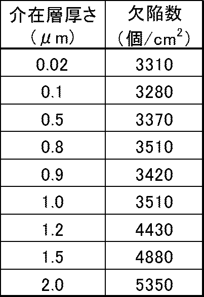
- the thickness of the silicon oxide thin film after polishing is 9 levels of 0.02, 0.1, 0.5, 0.8, 0.9, 1.0, 1.2, 1.5, and 2.0 ⁇ m. did.
- the plasma activated surface treatment was applied to the ion-implanted surface of the single crystal silicon carbide substrate and the thin film formation surface of the handle substrate, both were bonded to obtain a joined body.
- the bonded body is heated to 500 ° C., mechanical impact is applied to one end of the ion implantation region, and the ion implantation region is peeled off, and single crystal silicon carbide is formed on the amorphous silicon carbide wafer via the silicon oxide thin film.
- Nine composite substrates to which the thin film was transferred were obtained.
- the thickness of the single crystal silicon carbide thin film at this time was 0.95 ⁇ m.
- the obtained composite substrate was heated to 1,420 ° C. in an inert gas atmosphere to convert the single crystal silicon carbide thin film into graphene.
- the surface of the graphene film was observed with an optical microscope of 1,000 times, and the number of pit-like holes was visually measured as the number of defects.
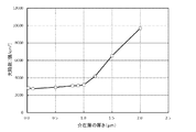
- the results are shown in Table 1 and FIG. When the thickness of the intervening layer was 1 ⁇ m or less, the number of defects was around 3000 / cm 2 , but when the thickness exceeded 1 ⁇ m, the number of defects increased to over 4000 / cm 2 .
- Example 2 As the single crystal silicon carbide substrate 1, a commercially available single crystal silicon carbide wafer having a diameter of 3 inches (polytype 4H, thickness 400 ⁇ m) is prepared, and 100 KeV and a dose amount of 8.8 ⁇ 10 16 atoms / cm 2 are prepared. Hydrogen ions (H + ) were implanted. Next, a titanium (Ti) thin film and a 10 nm thick gold (Au) thin film were formed on the ion-implanted surface of the single crystal silicon carbide substrate 1 as a thin film 3a by electron beam evaporation.
- Ni titanium
- Au gold
- the thickness of the titanium thin film was changed to nine levels of 0, 40, 240, 390, 440, 490, 590, 740, and 990 nm.
- a polycrystalline silicon carbide wafer (thickness: 400 ⁇ m) having a diameter of 3 inches is prepared as the handle substrate 12, and a titanium (Ti) thin film and gold (with a thickness of 10 nm) are formed on the main surface of the thin film 3 b by electron beam evaporation. Au) thin film was formed.
- the thickness of the titanium thin film was the same as the thickness of the titanium thin film in the thin film 3a.
- the total film thickness (thickness of the intervening layer 13) of the thin films 3a and 3b after bonding is 0.02, 0.1, 0.5, 0.8, 0.9, 1.0, 1 9 levels of 2, 1.5 and 2.0 ⁇ m.
- the plasma activation surface treatment was applied to the thin film formation surface of the single crystal silicon carbide substrate and the thin film formation surface of the handle substrate, both were bonded together to obtain a joined body.
- the bonded body is heated to 500 ° C., mechanical impact is applied to one end of the ion implantation region, and the ion implantation region is peeled off, and an intermediate layer (Au / Au two-layer structure) is formed on the amorphous silicon carbide wafer.
- the obtained composite substrate was heated to 1,420 ° C. in an inert gas atmosphere to convert the single crystal silicon carbide thin film into graphene.
- the surface of the graphene film was observed with an optical microscope of 1,000 times, and the number of pit-like holes was visually measured as the number of defects.
- the results are shown in Table 2 and FIG. When the thickness of the intervening layer was 1 ⁇ m or less, the number of defects was about 3300 to 3500 / cm 2 , but when the thickness exceeded 1 ⁇ m, the number of defects increased to over 4000 / cm 2 .
- Example 2 the thickness of the titanium thin film of each of the thin films 3a and 3b is set to 80 nm, and the thickness of the single crystal silicon carbide thin film 11 is set to 1.04 ⁇ m. Otherwise, the composite substrate is manufactured in the same manner as in Example 2. did. The obtained composite substrate was heated to 1,420 ° C. in an inert gas atmosphere to convert the single crystal silicon carbide thin film into graphene. After the graphene film was formed, the surface of the graphene film was observed with a 1,000 ⁇ optical microscope, and the number of pit-like holes was visually measured as the number of defects, which was 4520 / cm 2 .
- Example 3 In the method for manufacturing a composite substrate of the present invention, six types of thin films 3a and 3b were formed on the single crystal silicon carbide substrate 1 and the handle substrate 12, respectively, and the composite substrate was manufactured as follows.
- Example 3-1 As the single crystal silicon carbide substrate 1, a commercially available single crystal silicon carbide wafer having a diameter of 3 inches (polytype 4H, thickness 400 ⁇ m) is prepared, and 100 KeV and a dose amount of 8.8 ⁇ 10 16 atoms / cm 2 are prepared. Hydrogen ions (H + ) were implanted. Next, a silicon oxide (SiO 2 ) thin film having a thickness of 100 nm was formed as a thin film 3a on the ion-implanted surface of the single crystal silicon carbide substrate 1 by PECVD, and this thin film was polished by CMP treatment.
- SiO 2 silicon oxide
- a polycrystalline silicon carbide wafer (thickness: 400 ⁇ m) having a diameter of 3 inches was prepared as the handle substrate 12, and a silicon oxide (SiO 2 ) thin film having a thickness of 100 nm was formed as a thin film 3 b on the main surface by PECVD. Thereafter, this thin film was polished by CMP treatment. Next, after the plasma activation surface treatment was applied to the thin film formation surface of the single crystal silicon carbide substrate and the thin film formation surface of the handle substrate, both were bonded together to obtain a joined body.
- the bonded body was mechanically peeled off in the ion implantation region to obtain a composite substrate in which a single crystal silicon carbide thin film (thickness 0.65 ⁇ m) was transferred to a polycrystalline silicon carbide wafer via a silicon oxide thin film.
- the obtained composite substrate was subjected to a heat treatment at 500 ° C., and then an adhesive tape (trade name: Kapton Tape, manufactured by DuPont) was applied to the single crystal silicon carbide thin film and then peeled off.
- Kapton Tape trade name: Kapton Tape, manufactured by DuPont
- grapheneization was performed in the same manner as in Example 2, and the number of defects in the graphene film was measured. As a result, it was 3080 / cm 2 .
- Example 3-2 In Example 3-1, after forming a silicon nitride (SiN) thin film having a thickness of 100 nm as the thin films 3a and 3b by sputtering, the thin film is polished and finished by CMP treatment. A composite substrate was produced in the same manner as in 3-1. As a result, a composite substrate was obtained in which the single crystal silicon carbide thin film was transferred to the polycrystalline silicon carbide wafer via the silicon nitride thin film. When the obtained composite substrate was subjected to the same peel test as in Example 3-1, peeling of the single crystal silicon carbide thin film was not observed, and adhesion through the intervening layer was good. Subsequently, grapheneization was performed in the same manner as in Example 2, and the number of defects in the graphene film was measured to find 3480 pieces / cm 2 .
- SiN silicon nitride
- Example 3-3 In Example 3-1, an amorphous silicon carbide (SiC) thin film having a thickness of 100 nm was formed as each of the thin films 3a and 3b by sputtering, and then the thin film was polished and finished by CMP treatment.
- a composite substrate was produced in the same manner as in Example 3-1. As a result, a composite substrate was obtained in which the single crystal silicon carbide thin film was transferred to the polycrystalline silicon carbide wafer via the silicon carbide thin film.
- peeling of the single crystal silicon carbide thin film was not observed, and adhesion through the intervening layer was good.
- grapheneization was performed in the same manner as in Example 2, and the number of defects in the graphene film was measured. As a result, it was 3320 / cm 2 .
- Example 3-4 In Example 3-1, an amorphous silicon (Si) thin film having a thickness of 100 nm was formed as each of the thin films 3a and 3b by sputtering, and then the thin film was polished and finished by CMP treatment. A composite substrate was produced in the same manner as in 3-1. As a result, a composite substrate was obtained in which the single crystal silicon carbide thin film was transferred to the polycrystalline silicon carbide wafer via the silicon thin film. When the obtained composite substrate was subjected to the same peel test as in Example 3-1, peeling of the single crystal silicon carbide thin film was not observed, and adhesion through the intervening layer was good. Next, grapheneization was performed in the same manner as in Example 2, and the number of defects in the graphene film was measured. As a result, it was 3290 / cm 2 .
- Example 3-5 In Example 3-1, a thin film of titanium (Ti) having a thickness of 20 nm was formed as the thin films 3a and 3b by the electron beam evaporation method, respectively, and then left without being subjected to the CMP process. A composite substrate was produced in the same manner. As a result, a composite substrate was obtained in which the single crystal silicon carbide thin film was transferred to the polycrystalline silicon carbide wafer via the titanium thin film. When the obtained composite substrate was subjected to the same peel test as in Example 3-1, peeling of the single crystal silicon carbide thin film was not observed, and adhesion through the intervening layer was good. Next, grapheneization was performed in the same manner as in Example 2, and the number of defects in the graphene film was measured to be 3310 / cm 2 .
- Example 3-1 After forming a 20 nm-thick titanium (Ti) thin film and a 20 nm-thick gold (Au) thin film as the thin films 3a and 3b by the electron beam evaporation method, they are left without being subjected to CMP treatment. Otherwise, a composite substrate was produced in the same manner as in Example 3-1. As a result, a composite substrate was obtained in which a single crystal silicon carbide thin film was transferred to a polycrystalline silicon carbide wafer via a laminated thin film of titanium thin film and gold thin film (a thin film having a four-layer structure of Ti / Au / Au / Ti).
- Example 3-1 When the obtained composite substrate was subjected to the same peel test as in Example 3-1, peeling of the single crystal silicon carbide thin film was not observed, and adhesion through the intervening layer was good. Next, grapheneization was performed in the same manner as in Example 2, and the number of defects in the graphene film was measured. As a result, it was 2290 / cm 2 .
- Example 4 the handle substrate 12 was an amorphous silicon carbide wafer (thickness 400 ⁇ m) having a diameter of 3 inches, and a composite substrate was fabricated in the same manner as in Example 3 except that. Further, an example of zirconium oxide (zirconia, ZrO 2 ) was added as a material for the intervening layer. Details are as follows.
- Example 4-1 In Example 3-1, a composite substrate was fabricated in the same manner as in Example 3-1, except that the handle substrate 12 was an amorphous silicon carbide wafer having a diameter of 3 inches (thickness: 400 ⁇ m). As a result, a composite substrate was obtained in which the single crystal silicon carbide thin film was transferred to the amorphous silicon carbide wafer via the silicon oxide thin film. When the obtained composite substrate was subjected to the same peel test as in Example 3-1, peeling of the single crystal silicon carbide thin film was not observed, and adhesion through the intervening layer was good. Next, grapheneization was performed in the same manner as in Example 2, and the number of defects in the graphene film was measured. As a result, it was 3470 / cm 2 .
- Example 4-2 the handle substrate 12 was an amorphous silicon carbide wafer (thickness 400 ⁇ m) having a diameter of 3 inches, and a composite substrate was fabricated in the same manner as in Example 3-2.
- a composite substrate was obtained in which the single crystal silicon carbide thin film was transferred to the amorphous silicon carbide wafer via the silicon nitride thin film.
- peeling of the single crystal silicon carbide thin film was not observed, and adhesion through the intervening layer was good.
- grapheneization was performed in the same manner as in Example 2, and the number of defects in the graphene film was measured. As a result, it was 3220 / cm 2 .
- Example 4-3 the handle substrate 12 was an amorphous silicon carbide wafer (400 ⁇ m thickness) having a diameter of 3 inches, and a composite substrate was fabricated in the same manner as in Example 3-3. As a result, a composite substrate was obtained in which the single crystal silicon carbide thin film was transferred to the amorphous silicon carbide wafer via the silicon carbide thin film. When the obtained composite substrate was subjected to the same peel test as in Example 3-1, peeling of the single crystal silicon carbide thin film was not observed, and adhesion through the intervening layer was good. Next, grapheneization was performed in the same manner as in Example 2, and the number of defects in the graphene film was measured. As a result, it was 3400 / cm 2 .
- Example 4-4 the handle substrate 12 was an amorphous silicon carbide wafer (400 ⁇ m thick) having a diameter of 3 inches, and a composite substrate was fabricated in the same manner as in Example 3-4. As a result, a composite substrate was obtained in which the single crystal silicon carbide thin film was transferred to the amorphous silicon carbide wafer via the silicon thin film. When the obtained composite substrate was subjected to the same peel test as in Example 3-1, peeling of the single crystal silicon carbide thin film was not observed, and adhesion through the intervening layer was good. Subsequently, grapheneization was performed in the same manner as in Example 2, and the number of defects in the graphene film was measured to find 3360 / cm 2 .
- Example 4-5 a handle substrate 12 was an amorphous silicon carbide wafer (thickness 400 ⁇ m) having a diameter of 3 inches, and a composite substrate was fabricated in the same manner as in Example 3-5. As a result, a composite substrate was obtained in which the single crystal silicon carbide thin film was transferred to the amorphous silicon carbide wafer via the titanium thin film. When the obtained composite substrate was subjected to the same peel test as in Example 3-1, peeling of the single crystal silicon carbide thin film was not observed, and adhesion through the intervening layer was good. Next, grapheneization was performed in the same manner as in Example 2, and the number of defects in the graphene film was measured to be 3310 / cm 2 .
- Example 4-6 the handle substrate 12 was an amorphous silicon carbide wafer (400 ⁇ m thickness) having a diameter of 3 inches, and a composite substrate was fabricated in the same manner as in Example 3-6.
- a composite substrate was obtained in which the single-crystal silicon carbide thin film was transferred to the amorphous silicon carbide wafer via the laminated thin film (Ti / Au / Au / Ti four-layer thin film) of the titanium thin film and the gold thin film.
- the obtained composite substrate was subjected to the same peel test as in Example 3-1, peeling of the single crystal silicon carbide thin film was not observed, and adhesion through the intervening layer was good.
- grapheneization was performed in the same manner as in Example 2, and the number of defects in the graphene film was measured. As a result, it was 3020 / cm 2 .
- Example 4--7 In Example 4-1, as a thin film 3a, 3b, a zirconium oxide (ZrO 2 ) thin film having a thickness of 100 nm was formed by sputtering, and then this thin film was polished and finished by CMP treatment. A composite substrate was produced in the same manner as in Example 4-1. As a result, a composite substrate was obtained in which the single crystal silicon carbide thin film was transferred to the amorphous silicon carbide wafer via the zirconium oxide thin film. When the obtained composite substrate was subjected to the same peel test as in Example 3-1, peeling of the single crystal silicon carbide thin film was not observed, and adhesion through the intervening layer was good. Next, grapheneization was performed in the same manner as in Example 2, and the number of defects in the graphene film was measured to find 3530 / cm 2 .
- ZrO 2 zirconium oxide
- Example 5 In Example 3-6, a composite substrate was manufactured in the same manner as in Example 3-6 except that four types of handle substrates 12 were used. Details are as follows.
- Example 5-1 the handle substrate 12 was a single crystal silicon wafer (thickness 400 ⁇ m) having a diameter of 3 inches, and a composite substrate was fabricated in the same manner as in Example 3-6.
- a composite substrate was obtained in which a single crystal silicon carbide thin film was transferred to a single crystal silicon wafer via a laminated thin film of titanium thin film and gold thin film (a thin film having a four-layer structure of Ti / Au / Au / Ti).
- peeling of the single crystal silicon carbide thin film was not observed, and adhesion through the intervening layer was good.
- grapheneization was performed in the same manner as in Example 2, and the number of defects in the graphene film was measured. As a result, it was 3210 / cm 2 .
- Example 5-2 a composite substrate was fabricated in the same manner as in Example 3-6, except that the handle substrate 12 was a polycrystalline aluminum oxide (alumina) wafer having a diameter of 3 inches (thickness: 400 ⁇ m).
- a composite substrate was obtained in which a single crystal silicon carbide thin film was transferred to a polycrystalline aluminum oxide wafer via a laminated thin film of a titanium thin film and a gold thin film (a thin film having a four-layer structure of Ti / Au / Au / Ti).
- peeling of the single crystal silicon carbide thin film was not observed, and adhesion through the intervening layer was good.
- grapheneization was performed in the same manner as in Example 2, and the number of defects in the graphene film was measured. As a result, it was 3440 pieces / cm 2 .
- Example 5-3 the handle substrate 12 was a polycrystalline silicon nitride wafer (thickness 400 ⁇ m) having a diameter of 3 inches, and a composite substrate was fabricated in the same manner as in Example 3-6.
- a composite substrate was obtained in which a single crystal silicon carbide thin film was transferred to a polycrystalline silicon nitride wafer via a laminated thin film of a titanium thin film and a gold thin film (a thin film having a four-layer structure of Ti / Au / Au / Ti).
- peeling of the single crystal silicon carbide thin film was not observed, and adhesion through the intervening layer was good.
- grapheneization was performed in the same manner as in Example 2, and the number of defects in the graphene film was measured. As a result, it was 3330 / cm 2 .
- Example 5-4 In Example 3-6, a handle substrate 12 was a polycrystalline aluminum nitride wafer (thickness 400 ⁇ m) having a diameter of 3 inches, and a composite substrate was fabricated in the same manner as in Example 3-6. As a result, a composite substrate was obtained in which a single crystal silicon carbide thin film was transferred to a polycrystalline aluminum nitride wafer via a laminated thin film of a titanium thin film and a gold thin film (a thin film having a four-layer structure of Ti / Au / Au / Ti). When the obtained composite substrate was subjected to the same peel test as in Example 3-1, peeling of the single crystal silicon carbide thin film was not observed, and adhesion through the intervening layer was good. Next, grapheneization was performed in the same manner as in Example 2, and the number of defects in the graphene film was measured. As a result, it was 3490 / cm 2 .
- the single crystal silicon carbide substrate 1 As the single crystal silicon carbide substrate 1, a commercially available single crystal silicon carbide wafer having a diameter of 3 inches (polytype 4H, thickness 400 ⁇ m) is prepared, and 100 KeV and a dose amount of 8.8 ⁇ 10 16 atoms / cm 2 are prepared. Hydrogen ions (H + ) were implanted. The ion-implanted surface of this single crystal silicon carbide wafer was polished by CMP treatment. Its surface roughness RMS was 0.95 nm. The surface roughness RMS was obtained by measuring the surface of the substrate with an atomic force microscope (AFM). The measurement conditions were a measurement area of 10 ⁇ m ⁇ 10 ⁇ m.
- AFM atomic force microscope
- a polycrystalline silicon carbide wafer (thickness 400 ⁇ m) having a diameter of 3 inches was prepared as the handle substrate 12.
- the surface of this polycrystalline silicon carbide wafer was polished by CMP treatment, and its surface roughness RMS was 1.05 nm.
- plasma-activated surface treatment was performed on the ion-implanted surface of the single crystal silicon carbide substrate and the planned bonding surface of the handle substrate, and then both were bonded to obtain a joined body.
- this bonded body was mechanically peeled off in the ion implantation region to obtain a composite substrate in which a single crystal silicon carbide thin film was transferred to a polycrystalline silicon carbide wafer.
Landscapes
- Chemical & Material Sciences (AREA)
- Organic Chemistry (AREA)
- Engineering & Computer Science (AREA)
- Inorganic Chemistry (AREA)
- Ceramic Engineering (AREA)
- Materials Engineering (AREA)
- Nanotechnology (AREA)
- Crystallography & Structural Chemistry (AREA)
- Metallurgy (AREA)
- Physics & Mathematics (AREA)
- Plasma & Fusion (AREA)
- Thermal Sciences (AREA)
- Mechanical Engineering (AREA)
- Laminated Bodies (AREA)
- Crystals, And After-Treatments Of Crystals (AREA)
- Carbon And Carbon Compounds (AREA)
Abstract
Description
また、そのような構造の複合基板を用いてナノカーボン膜を形成すると、積層した単結晶炭化珪素薄膜、あるいはそこに形成されるナノカーボン膜に欠陥が発生する場合があった。それを詳細に調査したところ、上記介在層が厚いと上記欠陥が発生し易く、特に介在層の厚さが1μmを超えると欠陥が発生してしまうことが分かった。これは、介在層自身の膨張係数と単結晶炭化珪素薄膜の膨張係数との差から生じる歪によるものと考えられる。更に調査したところ、接合される単結晶炭化珪素薄膜そのものも薄い方が該単結晶炭化珪素薄膜やナノカーボン膜に発生する欠陥を抑制する効果が高いことが判明した。
本発明者らはこれらの知見を基に鋭意検討を行い、本発明を成すに至った。
〔1〕 厚さ1μm以下の単結晶炭化珪素薄膜と、該単結晶炭化珪素薄膜を支持する耐熱温度1100℃以上の耐熱材料(ただし、単結晶炭化珪素を除く)からなるハンドル基板と、上記単結晶炭化珪素薄膜とハンドル基板との間に設けられた、Ti、Au、Ag、Cu、Ni、Co、Fe、Cr、Zr、Mo、Ta及びWから選ばれる少なくとも1種の金属材料からなる厚さが1μm以下の介在層とを備える複合基板。
〔2〕 上記ハンドル基板は、アモルファス炭化珪素、多結晶炭化珪素、石英ガラス、サファイア、窒化珪素、窒化アルミニウム、シリコン又はダイヤモンドからなることを特徴とする〔1〕記載の複合基板。
〔3〕 厚さ1μm以下の単結晶炭化珪素薄膜と、該単結晶炭化珪素薄膜を支持する耐熱温度1100℃以上の耐熱材料(ただし、単結晶炭化珪素を除く)からなるハンドル基板と、上記単結晶炭化珪素薄膜とハンドル基板との間に設けられた、酸化珪素、窒化珪素、酸化アルミニウム、窒化アルミニウム、酸化ジルコニウム、シリコン及び炭化珪素から選ばれる少なくとも1種の材料からなる厚さが1μm以下の介在層とを備える複合基板。
〔4〕 上記ハンドル基板は、アモルファス炭化珪素、多結晶炭化珪素又は石英ガラスからなることを特徴とする〔3〕記載の複合基板。
〔5〕 上記単結晶炭化珪素薄膜は、単結晶炭化珪素基板からその一部を剥離させて形成したものである〔1〕~〔4〕のいずれかに記載の複合基板。
〔6〕 〔1〕又は〔2〕記載の複合基板を加熱して上記単結晶炭化珪素薄膜から珪素原子を昇華させてナノカーボン膜を得ることを特徴とするナノカーボン膜の作製方法。
〔7〕 〔3〕又は〔4〕記載の複合基板を加熱して上記単結晶炭化珪素薄膜から珪素原子を昇華させてナノカーボン膜を得ることを特徴とするナノカーボン膜の作製方法。
〔8〕 〔6〕又は〔7〕記載のナノカーボン膜の作製方法により得られたナノカーボン膜。
〔9〕 1000倍の光学顕微鏡で表面観察した場合の欠陥数が4000個/cm2以下であることを特徴とする〔8〕記載のナノカーボン膜。
以下に、本発明に係る複合基板について説明する。
本発明に係る複合基板10は、図1に示すように、厚さ1μm以下の単結晶炭化珪素薄膜11と、該単結晶炭化珪素薄膜11を支持する耐熱温度1100℃以上の耐熱材料(ただし、単結晶炭化珪素を除く)からなるハンドル基板12と、上記単結晶炭化珪素薄膜11とハンドル基板12との間に設けられた、酸化珪素、窒化珪素、酸化アルミニウム、窒化アルミニウム、酸化ジルコニウム、シリコン及び炭化珪素から選ばれる少なくとも1種の材料、又はTi、Au、Ag、Cu、Ni、Co、Fe、Cr、Zr、Mo、Ta及びWから選ばれる少なくとも1種の金属材料からなる厚さが1μm以下の介在層13とを備える。
本発明の複合基板10は、ナノカーボン膜形成用、即ち加熱により単結晶炭化珪素薄膜11から珪素原子を昇華させてハンドル基板12に介在層13を介して支持された単結晶炭化珪素薄膜11にナノカーボン膜を形成するためのものである。詳しくは、複合基板10を好ましくは1,100℃以上、より好ましくは1,200~1,400℃、更に好ましくは1,250~1,350℃に加熱することにより単結晶炭化珪素薄膜11を構成する炭化珪素(SiC)から珪素原子(Si)を昇華させて、厚さ20~1,000nm程度のナノカーボン膜を形成することができる。この加熱処理の雰囲気は真空雰囲気(減圧)にすると珪素原子が昇華されやすいので好ましい。また、このときの温度条件も雰囲気や処理枚数等により変化するので適宜最適な温度に設定をする。
本発明の複合基板の製造方法について説明する。
本発明に係る複合基板の製造方法は、図2に示すように、単結晶炭化珪素基板への水素イオン注入工程(工程1)、単結晶炭化水素基板のイオン注入面への薄膜形成工程(工程2)、ハンドル基板への薄膜形成工程(工程3)、単結晶炭化珪素基板及び/又はハンドル基板の表面活性化処理工程(工程4)、単結晶炭化珪素基板とハンドル基板との貼り合わせ工程(工程5)、剥離処理工程(工程6)、単結晶炭化珪素薄膜研磨工程(工程7)の順に処理を行うものである。
まず、単結晶炭化珪素基板1に水素イオン等を注入してイオン注入領域2を形成する(図2(a))。
イオン注入深さは、単結晶炭化珪素薄膜の厚さに対応するものである。
本工程では以下の工程2-1、工程2-2のいずれかを行い、単結晶炭化珪素基板1の貼り合わせを行う面に薄膜3aを形成する。
単結晶炭化珪素基板1のイオン注入面に、後に行われる熱処理に対する耐熱性を有し、最終的に形成される単結晶炭化珪素薄膜11と同じか又は近い熱膨張係数を有する材料からなる薄膜3aを形成する。薄膜3aを構成する材料としては、酸化珪素(例えば、SiO2)、窒化珪素、窒化アルミニウム、シリコン(例えば、アモルファスシリコン、多結晶シリコン)、アルミナ(Al2O3)、酸化ジルコニウム(例えば、ジルコニア(ZrO2))及び炭化珪素(例えば、アモルファス炭化珪素、多結晶炭化珪素)から選ばれる少なくとも1種の材料が挙げられる。これらのうち、酸化ジルコニウム(例えば、ジルコニア(ZrO2))又は炭化珪素(例えば、アモルファス炭化珪素、多結晶炭化珪素)が好ましい。なお、これらの材料から複数の材料が選ばれた場合には、それらの材料ごとに積層した構造、それらの材料を混合した材料からなる単層構造のいずれでもよい。
単結晶炭化珪素基板1のイオン注入面に、融点が950℃以上の金属材料、例えばTi、Au、Ag、Cu、Ni、Co、Fe、Cr、Zr、Mo、Ta及びWから選ばれる少なくとも1種の金属材料からなる薄膜3aを形成する。なお、これらの金属材料から複数の金属材料が選ばれた場合には、それらの金属材料ごとに積層した構造、それらの金属材料の合金材料からなる単層構造のいずれでもよい。例えばこれらのうち、Ti、Au及びZrから選ばれる少なくとも1種が好ましく、特にTiやZrの単層、あるいはTi層とAu層の積層、Zr層とAu層の積層が好ましい。
本工程で用いるハンドル基板12は、上述した複合基板10を構成するハンドル基板と同じである。
即ち、工程2-1に対応する処理としては、次のように行う。
まず、ハンドル基板12における単結晶炭化珪素基板1との貼り合わせ面に、酸化珪素(例えば、SiO2)、窒化珪素、窒化アルミニウム、シリコン(例えば、アモルファスシリコン、多結晶シリコン)、アルミナ(Al2O3)、酸化ジルコニウム(例えば、ジルコニア(ZrO2))及び炭化珪素(例えば、アモルファス炭化珪素、多結晶炭化珪素)から選ばれる少なくとも1種の材料からなる薄膜3bを形成する。これらのうち、酸化ジルコニウム(例えば、ジルコニア(ZrO2))又は炭化珪素(例えば、アモルファス炭化珪素、多結晶炭化珪素)が好ましい。なお、これらの材料から複数の材料が選ばれた場合には、それらの材料ごとに積層した構造、それらの材料を混合した材料からなる単層構造のいずれでもよい。
ハンドル基板12の単結晶炭化珪素基板1との貼り合わせ面(主面)に、融点が950℃以上の金属材料、例えばTi、Au、Ag、Cu、Ni、Co、Fe、Cr、Zr、Mo、Ta及びWから選ばれる少なくとも1種の金属材料からなる薄膜3bを形成する。なお、これらの金属材料から複数の金属材料が選ばれた場合には、それらの金属材料ごとに積層した構造、それらの金属材料の合金材料からなる単層構造のいずれでもよい。例えばこれらのうち、Ti、Au及びZrから選ばれる少なくとも1種が好ましく、特にTiやZrの単層、あるいはTi層とAu層の積層、Zr層とAu層の積層が好ましい。
次に、単結晶炭化珪素基板1とハンドル基板12の貼り合わせをする表面、即ち薄膜3a、3b表面、あるいは単結晶炭化珪素基板1のイオン注入面、ハンドル基板12表面について、表面活性化処理としてプラズマ活性化処理、真空イオンビーム処理又はオゾン水への浸漬処理を行う。
次に、この単結晶炭化珪素基板1及びハンドル基板12の表面活性化処理をした表面(薄膜3a、3b表面、あるいは単結晶炭化珪素基板1のイオン注入面、ハンドル基板12表面)を接合面として貼り合わせる(図2(d))。
単結晶炭化珪素基板1とハンドル基板12とを貼り合わせ、貼り合わせ強度を向上させた後、イオン注入した部分に熱的エネルギー又は機械的エネルギーを付与して、イオン注入領域2で単結晶炭化珪素基板1aを剥離させ、ハンドル基板12上に単結晶炭化珪素薄膜1bを有する複合基板10を作製する(図2(e))。
ハンドル基板12上の単結晶炭化珪素薄膜1b表面を鏡面仕上げする(図2(f))。具体的には、単結晶炭化珪素薄膜1bに化学機械研磨(CMP研磨)を施してその表面に残っているイオン注入領域を除去し鏡面の単結晶炭化珪素薄膜11に仕上げる。ここではシリコンウェハの平坦化等に用いられる従来公知のCMP研磨でよい。
なお、単結晶炭化珪素薄膜及び介在層の厚さは、反射率分光法により測定した。
単結晶炭化珪素基板1として、市販品の直径3インチの単結晶炭化珪素ウェーハ(ポリタイプ4H、厚さ400μm)を用意し、これに100KeV,ドーズ量8.8×10¹⁶atom/cm2で水素イオン(H+)を注入した。
次に、ハンドル基板12として、直径3インチのアモルファス炭化珪素ウェーハ(厚さ400μm)を用意し、その主面に薄膜3b(介在層13)としてPECVD法によっての酸化珪素(SiO2)薄膜をその厚さを変化させて形成した後、この薄膜をCMP処理により研磨した。研磨後の酸化珪素薄膜の厚さは、0.02、0.1、0.5、0.8、0.9、1.0、1.2、1.5、2.0μmの9水準とした。
次いで、単結晶炭化珪素基板のイオン注入した表面及びハンドル基板の薄膜形成面にプラズマ活性化表面処理を施した後、両者を貼り合わせて接合体を得た。
次いで、この接合体を500℃に加熱し、イオン注入領域の一端に機械的衝撃を付与して、このイオン注入領域で剥離させて、アモルファス炭化珪素ウェーハに酸化珪素薄膜を介して単結晶炭化珪素薄膜が転写された9枚の複合基板を得た。このときの単結晶炭化珪素薄膜の厚さをいずれも0.95μmとした。
グラフェン膜形成後にそのグラフェン膜表面を1,000倍の光学顕微鏡で観察して欠陥数としてピット状の穴の数を目視で計測した。その結果を表1及び図3に示す。介在層の厚さが1μm以下では欠陥数が3000個/cm2前後であったが、1μmを超えると欠陥数が4000個/cm2超に増加した。

単結晶炭化珪素基板1として、市販品の直径3インチの単結晶炭化珪素ウェーハ(ポリタイプ4H、厚さ400μm)を用意し、これに100KeV,ドーズ量8.8×10¹⁶atom/cm2で水素イオン(H+)を注入した。
次いで、この単結晶炭化珪素基板1のイオン注入面に薄膜3aとして電子ビーム蒸着法によってチタン(Ti)薄膜と厚さ10nmの金(Au)薄膜を形成した。なお、チタン薄膜の厚さを0、40、240、390、440、490、590、740、990nmの9水準に変化させた。
次に、ハンドル基板12として、直径3インチの多結晶炭化珪素ウェーハ(厚さ400μm)を用意し、その主面に薄膜3bとして電子ビーム蒸着法によってチタン(Ti)薄膜と厚さ10nmの金(Au)薄膜を形成した。なお、チタン薄膜の厚さを上記薄膜3aにおけるチタン薄膜の厚さと同じとした。その結果、貼り合わせ後の薄膜3a、3bの合計膜厚(介在層13の厚さ)は、0.02、0.1、0.5、0.8、0.9、1.0、1.2、1.5、2.0μmの9水準となる。
次いで、単結晶炭化珪素基板の薄膜形成面及びハンドル基板の薄膜形成面にプラズマ活性化表面処理を施した後、両者を貼り合わせて接合体を得た。
次いで、この接合体を500℃に加熱し、イオン注入領域の一端に機械的衝撃を付与して、このイオン注入領域で剥離させて、アモルファス炭化珪素ウェーハに介在層(Au/Auの2層構造又はTi/Au/Au/Tiの4層構造の薄膜)を介して単結晶炭化珪素薄膜が転写された9枚の複合基板を得た。このときの単結晶炭化珪素薄膜の厚さをいずれも0.95μmとした。
グラフェン膜形成後にそのグラフェン膜表面を1,000倍の光学顕微鏡で観察して欠陥数としてピット状の穴の数を目視で計測した。その結果を表2及び図4に示す。介在層の厚さが1μm以下では欠陥数が3300~3500個/cm2程度であったが、1μmを超えると欠陥数が4000個/cm2超に増加した。
実施例2において、薄膜3a、3bそれぞれのチタン薄膜の厚さを80nmとし、更に単結晶炭化珪素薄膜11の厚さを1.04μmとし、それ以外は実施例2と同様にして複合基板を作製した。
得られた複合基板を不活性ガス雰囲気下で1,420℃に加熱して、単結晶炭化珪素薄膜のグラフェン化を行った。
グラフェン膜形成後にそのグラフェン膜表面を1,000倍の光学顕微鏡で観察して欠陥数としてピット状の穴の数を目視で計測したところ、4520個/cm2であった。
本発明の複合基板の製造方法において、単結晶炭化珪素基板1、ハンドル基板12それぞれに6種類の薄膜3a、3bを形成して、複合基板を以下のように作製した。
単結晶炭化珪素基板1として、市販品の直径3インチの単結晶炭化珪素ウェーハ(ポリタイプ4H、厚さ400μm)を用意し、これに100KeV,ドーズ量8.8×10¹⁶atom/cm2で水素イオン(H+)を注入した。
次いで、この単結晶炭化珪素基板1のイオン注入面に薄膜3aとしてPECVD法によって厚さ100nmの酸化珪素(SiO2)薄膜を形成した後、この薄膜をCMP処理により研磨した。
次に、ハンドル基板12として、直径3インチの多結晶炭化珪素ウェーハ(厚さ400μm)を用意し、その主面に薄膜3bとしてPECVD法によって厚さ100nmの酸化珪素(SiO2)薄膜を形成した後、この薄膜をCMP処理により研磨した。
次いで、単結晶炭化珪素基板の薄膜形成面及びハンドル基板の薄膜形成面にプラズマ活性化表面処理を施した後、両者を貼り合わせて接合体を得た。
次いで、この接合体についてイオン注入領域にて機械剥離を起こし、多結晶炭化珪素ウェーハに酸化珪素薄膜を介して単結晶炭化珪素薄膜(厚さ0.65μm)が転写された複合基板を得た。
得られた複合基板について500℃の熱処理を施した後、粘着テープ(商品名:カプトンテープ、デュポン(株)製)を単結晶炭化珪素薄膜に貼った後に引き剥し、該単結晶炭化珪素薄膜の剥離の有無を確認するピールテストを行ったところ、単結晶炭化珪素薄膜の剥離は認められず、介在層を介しての密着性は良好であった。
次いで、実施例2と同様にグラフェン化を行い、グラフェン膜における欠陥数を測定したところ、3080個/cm2であった。
実施例3-1において、薄膜3a、3bとして、それぞれスパッタリング法によって厚さ100nmの窒化珪素(SiN)薄膜を形成した後、この薄膜をCMP処理により研磨して仕上げるようにし、それ以外は実施例3-1と同様にして複合基板を作製した。
その結果、多結晶炭化珪素ウェーハに窒化珪素薄膜を介して単結晶炭化珪素薄膜が転写された複合基板を得た。得られた複合基板について、実施例3-1と同様のピールテストを行ったところ、単結晶炭化珪素薄膜の剥離は認められず、介在層を介しての密着性は良好であった。
次いで、実施例2と同様にグラフェン化を行い、グラフェン膜における欠陥数を測定したところ、3480個/cm2であった。
実施例3-1において、薄膜3a、3bとして、それぞれスパッタリング法によって厚さ100nmのアモルファス炭化珪素(SiC)薄膜を形成した後、この薄膜をCMP処理により研磨して仕上げるようにし、それ以外は実施例3-1と同様にして複合基板を作製した。
その結果、多結晶炭化珪素ウェーハに炭化珪素薄膜を介して単結晶炭化珪素薄膜が転写された複合基板を得た。得られた複合基板について、実施例3-1と同様のピールテストを行ったところ、単結晶炭化珪素薄膜の剥離は認められず、介在層を介しての密着性は良好であった。
次いで、実施例2と同様にグラフェン化を行い、グラフェン膜における欠陥数を測定したところ、3320個/cm2であった。
実施例3-1において、薄膜3a、3bとして、それぞれスパッタリング法によって厚さ100nmのアモルファスシリコン(Si)薄膜を形成した後、この薄膜をCMP処理により研磨して仕上げるようにし、それ以外は実施例3-1と同様にして複合基板を作製した。
その結果、多結晶炭化珪素ウェーハにシリコン薄膜を介して単結晶炭化珪素薄膜が転写された複合基板を得た。得られた複合基板について、実施例3-1と同様のピールテストを行ったところ、単結晶炭化珪素薄膜の剥離は認められず、介在層を介しての密着性は良好であった。
次いで、実施例2と同様にグラフェン化を行い、グラフェン膜における欠陥数を測定したところ、3290個/cm2であった。
実施例3-1において、薄膜3a、3bとして、それぞれ電子ビーム蒸着法によって厚さ20nmのチタン(Ti)薄膜を形成した後、CMP処理することなくそのままとし、それ以外は実施例3-1と同様にして複合基板を作製した。
その結果、多結晶炭化珪素ウェーハにチタン薄膜を介して単結晶炭化珪素薄膜が転写された複合基板を得た。得られた複合基板について、実施例3-1と同様のピールテストを行ったところ、単結晶炭化珪素薄膜の剥離は認められず、介在層を介しての密着性は良好であった。
次いで、実施例2と同様にグラフェン化を行い、グラフェン膜における欠陥数を測定したところ、3310個/cm2であった。
実施例3-1において、薄膜3a、3bとして、それぞれ電子ビーム蒸着法によって厚さ20nmのチタン(Ti)薄膜と厚さ20nmの金(Au)薄膜を形成した後、CMP処理することなくそのままとし、それ以外は実施例3-1と同様にして複合基板を作製した。
その結果、多結晶炭化珪素ウェーハにチタン薄膜と金薄膜の積層薄膜(Ti/Au/Au/Tiの4層構造の薄膜)を介して単結晶炭化珪素薄膜が転写された複合基板を得た。得られた複合基板について、実施例3-1と同様のピールテストを行ったところ、単結晶炭化珪素薄膜の剥離は認められず、介在層を介しての密着性は良好であった。
次いで、実施例2と同様にグラフェン化を行い、グラフェン膜における欠陥数を測定したところ、2290個/cm2であった。
実施例3において、ハンドル基板12を直径3インチのアモルファス炭化珪素ウェーハ(厚さ400μm)とし、それ以外は実施例3と同様にして複合基板を作製した。また、介在層の材料として酸化ジルコニウム(ジルコニア、ZrO2)の実施例を追加した。詳しくは以下の通りである。
実施例3-1において、ハンドル基板12を直径3インチのアモルファス炭化珪素ウェーハ(厚さ400μm)とし、それ以外は実施例3-1と同様にして複合基板を作製した。
その結果、アモルファス炭化珪素ウェーハに酸化珪素薄膜を介して単結晶炭化珪素薄膜が転写された複合基板を得た。得られた複合基板について、実施例3-1と同様のピールテストを行ったところ、単結晶炭化珪素薄膜の剥離は認められず、介在層を介しての密着性は良好であった。
次いで、実施例2と同様にグラフェン化を行い、グラフェン膜における欠陥数を測定したところ、3470個/cm2であった。
実施例3-2において、ハンドル基板12を直径3インチのアモルファス炭化珪素ウェーハ(厚さ400μm)とし、それ以外は実施例3-2と同様にして複合基板を作製した。
その結果、アモルファス炭化珪素ウェーハに窒化珪素薄膜を介して単結晶炭化珪素薄膜が転写された複合基板を得た。得られた複合基板について、実施例3-1と同様のピールテストを行ったところ、単結晶炭化珪素薄膜の剥離は認められず、介在層を介しての密着性は良好であった。
次いで、実施例2と同様にグラフェン化を行い、グラフェン膜における欠陥数を測定したところ、3220個/cm2であった。
実施例3-3において、ハンドル基板12を直径3インチのアモルファス炭化珪素ウェーハ(厚さ400μm)とし、それ以外は実施例3-3と同様にして複合基板を作製した。
その結果、アモルファス炭化珪素ウェーハに炭化珪素薄膜を介して単結晶炭化珪素薄膜が転写された複合基板を得た。得られた複合基板について、実施例3-1と同様のピールテストを行ったところ、単結晶炭化珪素薄膜の剥離は認められず、介在層を介しての密着性は良好であった。
次いで、実施例2と同様にグラフェン化を行い、グラフェン膜における欠陥数を測定したところ、3400個/cm2であった。
実施例3-4において、ハンドル基板12を直径3インチのアモルファス炭化珪素ウェーハ(厚さ400μm)とし、それ以外は実施例3-4と同様にして複合基板を作製した。
その結果、アモルファス炭化珪素ウェーハにシリコン薄膜を介して単結晶炭化珪素薄膜が転写された複合基板を得た。得られた複合基板について、実施例3-1と同様のピールテストを行ったところ、単結晶炭化珪素薄膜の剥離は認められず、介在層を介しての密着性は良好であった。
次いで、実施例2と同様にグラフェン化を行い、グラフェン膜における欠陥数を測定したところ、3360個/cm2であった。
実施例3-5において、ハンドル基板12を直径3インチのアモルファス炭化珪素ウェーハ(厚さ400μm)とし、それ以外は実施例3-5と同様にして複合基板を作製した。
その結果、アモルファス炭化珪素ウェーハにチタン薄膜を介して単結晶炭化珪素薄膜が転写された複合基板を得た。得られた複合基板について、実施例3-1と同様のピールテストを行ったところ、単結晶炭化珪素薄膜の剥離は認められず、介在層を介しての密着性は良好であった。
次いで、実施例2と同様にグラフェン化を行い、グラフェン膜における欠陥数を測定したところ、3310個/cm2であった。
実施例3-6において、ハンドル基板12を直径3インチのアモルファス炭化珪素ウェーハ(厚さ400μm)とし、それ以外は実施例3-6と同様にして複合基板を作製した。
その結果、アモルファス炭化珪素ウェーハにチタン薄膜と金薄膜の積層薄膜(Ti/Au/Au/Tiの4層構造の薄膜)を介して単結晶炭化珪素薄膜が転写された複合基板を得た。得られた複合基板について、実施例3-1と同様のピールテストを行ったところ、単結晶炭化珪素薄膜の剥離は認められず、介在層を介しての密着性は良好であった。
次いで、実施例2と同様にグラフェン化を行い、グラフェン膜における欠陥数を測定したところ、3020個/cm2であった。
実施例4-1において、薄膜3a、3bとして、それぞれスパッタリング法によって厚さ100nmの酸化ジルコニウム(ZrO2)薄膜を形成した後、この薄膜をCMP処理により研磨して仕上げるようにし、それ以外は実施例4-1と同様にして複合基板を作製した。
その結果、アモルファス炭化珪素ウェーハに酸化ジルコニウム薄膜を介して単結晶炭化珪素薄膜が転写された複合基板を得た。得られた複合基板について、実施例3-1と同様のピールテストを行ったところ、単結晶炭化珪素薄膜の剥離は認められず、介在層を介しての密着性は良好であった。
次いで、実施例2と同様にグラフェン化を行い、グラフェン膜における欠陥数を測定したところ、3530個/cm2であった。
実施例3-6において、4種類のハンドル基板12を用い、それ以外は実施例3-6と同様にして複合基板を作製した。詳しくは以下の通りである。
実施例3-6において、ハンドル基板12を直径3インチの単結晶シリコンウェーハ(厚さ400μm)とし、それ以外は実施例3-6と同様にして複合基板を作製した。
その結果、単結晶シリコンウェーハにチタン薄膜と金薄膜の積層薄膜(Ti/Au/Au/Tiの4層構造の薄膜)を介して単結晶炭化珪素薄膜が転写された複合基板を得た。得られた複合基板について、実施例3-1と同様のピールテストを行ったところ、単結晶炭化珪素薄膜の剥離は認められず、介在層を介しての密着性は良好であった。
次いで、実施例2と同様にグラフェン化を行い、グラフェン膜における欠陥数を測定したところ、3210個/cm2であった。
実施例3-6において、ハンドル基板12を直径3インチの多結晶酸化アルミニウム(アルミナ)ウェーハ(厚さ400μm)とし、それ以外は実施例3-6と同様にして複合基板を作製した。
その結果、多結晶酸化アルミニウムウェーハにチタン薄膜と金薄膜の積層薄膜(Ti/Au/Au/Tiの4層構造の薄膜)を介して単結晶炭化珪素薄膜が転写された複合基板を得た。得られた複合基板について、実施例3-1と同様のピールテストを行ったところ、単結晶炭化珪素薄膜の剥離は認められず、介在層を介しての密着性は良好であった。
次いで、実施例2と同様にグラフェン化を行い、グラフェン膜における欠陥数を測定したところ、3440個/cm2であった。
実施例3-6において、ハンドル基板12を直径3インチの多結晶窒化珪素ウェーハ(厚さ400μm)とし、それ以外は実施例3-6と同様にして複合基板を作製した。
その結果、多結晶窒化珪素ウェーハにチタン薄膜と金薄膜の積層薄膜(Ti/Au/Au/Tiの4層構造の薄膜)を介して単結晶炭化珪素薄膜が転写された複合基板を得た。得られた複合基板について、実施例3-1と同様のピールテストを行ったところ、単結晶炭化珪素薄膜の剥離は認められず、介在層を介しての密着性は良好であった。
次いで、実施例2と同様にグラフェン化を行い、グラフェン膜における欠陥数を測定したところ、3330個/cm2であった。
実施例3-6において、ハンドル基板12を直径3インチの多結晶窒化アルミニウムウェーハ(厚さ400μm)とし、それ以外は実施例3-6と同様にして複合基板を作製した。
その結果、多結晶窒化アルミニウムウェーハにチタン薄膜と金薄膜の積層薄膜(Ti/Au/Au/Tiの4層構造の薄膜)を介して単結晶炭化珪素薄膜が転写された複合基板を得た。得られた複合基板について、実施例3-1と同様のピールテストを行ったところ、単結晶炭化珪素薄膜の剥離は認められず、介在層を介しての密着性は良好であった。
次いで、実施例2と同様にグラフェン化を行い、グラフェン膜における欠陥数を測定したところ、3490個/cm2であった。
単結晶炭化珪素基板1として、市販品の直径3インチの単結晶炭化珪素ウェーハ(ポリタイプ4H、厚さ400μm)を用意し、これに100KeV,ドーズ量8.8×10¹⁶atom/cm2で水素イオン(H+)を注入した。この単結晶炭化珪素ウェーハのイオン注入面をCMP処理で研磨した。その表面粗さRMSは0.95nmであった。
なお、表面粗さRMSは、原子間力顕微鏡(AFM)によりその基板の表面を測定して求めた。測定条件は、測定領域10μm×10μmとした。
次に、ハンドル基板12として、直径3インチの多結晶炭化珪素ウェーハ(厚さ400μm)を用意した。この多結晶炭化珪素ウェーハ表面をCMP処理で研磨し、その表面粗さRMSが1.05nmであった。
次いで、単結晶炭化珪素基板のイオン注入した表面及びハンドル基板の貼り合わせ予定面にプラズマ活性化表面処理を施した後、両者を貼り合わせて接合体を得た。
次いで、この接合体についてイオン注入領域にて機械剥離を起こし、多結晶炭化珪素ウェーハに単結晶炭化珪素薄膜が転写された複合基板を得た。
得られた複合基板について、実施例3-1と同様のピールテストを行ったところ、単結晶炭化珪素薄膜の一部に剥離が発生した。介在層を介していない貼り合わせでは単結晶炭化珪素薄膜とハンドル基板との間で十分な接合強度が得られないことが判明した。
1b、11 単結晶炭化珪素薄膜
2 イオン注入領域
3a、3b 薄膜
5 貼り合わせ基板
10 複合基板
12 ハンドル基板
13 介在層
Claims (9)
- 厚さ1μm以下の単結晶炭化珪素薄膜と、該単結晶炭化珪素薄膜を支持する耐熱温度1100℃以上の耐熱材料(ただし、単結晶炭化珪素を除く)からなるハンドル基板と、上記単結晶炭化珪素薄膜とハンドル基板との間に設けられた、Ti、Au、Ag、Cu、Ni、Co、Fe、Cr、Zr、Mo、Ta及びWから選ばれる少なくとも1種の金属材料からなる厚さが1μm以下の介在層とを備える複合基板。
- 上記ハンドル基板は、アモルファス炭化珪素、多結晶炭化珪素、石英ガラス、サファイア、窒化珪素、窒化アルミニウム、シリコン又はダイヤモンドからなることを特徴とする請求項1記載の複合基板。
- 厚さ1μm以下の単結晶炭化珪素薄膜と、該単結晶炭化珪素薄膜を支持する耐熱温度1100℃以上の耐熱材料(ただし、単結晶炭化珪素を除く)からなるハンドル基板と、上記単結晶炭化珪素薄膜とハンドル基板との間に設けられた、酸化珪素、窒化珪素、酸化アルミニウム、窒化アルミニウム、酸化ジルコニウム、シリコン及び炭化珪素から選ばれる少なくとも1種の材料からなる厚さが1μm以下の介在層とを備える複合基板。
- 上記ハンドル基板は、アモルファス炭化珪素、多結晶炭化珪素又は石英ガラスからなることを特徴とする請求項3記載の複合基板。
- 上記単結晶炭化珪素薄膜は、単結晶炭化珪素基板からその一部を剥離させて形成したものである請求項1~4のいずれか1項に記載の複合基板。
- 請求項1又は2記載の複合基板を加熱して上記単結晶炭化珪素薄膜から珪素原子を昇華させてナノカーボン膜を得ることを特徴とするナノカーボン膜の作製方法。
- 請求項3又は4記載の複合基板を加熱して上記単結晶炭化珪素薄膜から珪素原子を昇華させてナノカーボン膜を得ることを特徴とするナノカーボン膜の作製方法。
- 請求項6又は7記載のナノカーボン膜の作製方法により得られたナノカーボン膜。
- 1000倍の光学顕微鏡で表面観察した場合の欠陥数が4000個/cm2以下であることを特徴とする請求項8記載のナノカーボン膜。
Priority Applications (6)
| Application Number | Priority Date | Filing Date | Title |
|---|---|---|---|
| SG11201704904WA SG11201704904WA (en) | 2014-12-22 | 2015-12-16 | Composite substrate, method for forming nanocarbon film, and nanocarbon film |
| CN201580070163.XA CN107108218A (zh) | 2014-12-22 | 2015-12-16 | 复合基板、纳米碳膜的制作方法和纳米碳膜 |
| KR1020177017252A KR102427272B1 (ko) | 2014-12-22 | 2015-12-16 | 복합 기판, 나노카본막의 제작 방법 및 나노카본막 |
| US15/534,652 US10781104B2 (en) | 2014-12-22 | 2015-12-16 | Composite substrate, method for forming nanocarbon film, and nanocarbon film |
| JP2016566156A JP6369566B2 (ja) | 2014-12-22 | 2015-12-16 | ナノカーボン膜作製用複合基板及びナノカーボン膜の作製方法 |
| EP15872860.0A EP3239100A4 (en) | 2014-12-22 | 2015-12-16 | Composite substrate, method for forming nanocarbon film, and nanocarbon film |
Applications Claiming Priority (2)
| Application Number | Priority Date | Filing Date | Title |
|---|---|---|---|
| JP2014258810 | 2014-12-22 | ||
| JP2014-258810 | 2014-12-22 |
Publications (1)
| Publication Number | Publication Date |
|---|---|
| WO2016104291A1 true WO2016104291A1 (ja) | 2016-06-30 |
Family
ID=56150314
Family Applications (1)
| Application Number | Title | Priority Date | Filing Date |
|---|---|---|---|
| PCT/JP2015/085237 Ceased WO2016104291A1 (ja) | 2014-12-22 | 2015-12-16 | 複合基板、ナノカーボン膜の作製方法及びナノカーボン膜 |
Country Status (8)
| Country | Link |
|---|---|
| US (1) | US10781104B2 (ja) |
| EP (1) | EP3239100A4 (ja) |
| JP (1) | JP6369566B2 (ja) |
| KR (1) | KR102427272B1 (ja) |
| CN (2) | CN111403265A (ja) |
| SG (1) | SG11201704904WA (ja) |
| TW (1) | TWI673177B (ja) |
| WO (1) | WO2016104291A1 (ja) |
Cited By (6)
| Publication number | Priority date | Publication date | Assignee | Title |
|---|---|---|---|---|
| US20210032772A1 (en) * | 2018-03-28 | 2021-02-04 | Soitec | Method for producing a single-crystal film of aln material and substrate for the epitaxial growth of a single-crystal film of aln material |
| JP2022542224A (ja) * | 2019-08-01 | 2022-09-30 | ソイテック | 多結晶炭化ケイ素で作られたキャリア基板上に単結晶炭化ケイ素の薄層を含む複合構造を製造するためのプロセス |
| JP2022548171A (ja) * | 2019-09-17 | 2022-11-16 | 東京エレクトロン株式会社 | 高度回路アーキテクチャのための高密度ロジック及びメモリの製造方法 |
| JP2023528784A (ja) * | 2020-06-09 | 2023-07-06 | ソイテック | 非常に高い温度に対応する剥離可能な仮基板、及び前記基板から加工層を移動させるプロセス |
| WO2023176648A1 (ja) * | 2022-03-15 | 2023-09-21 | Agc株式会社 | 複合基板、積層体、複合基板の製造方法、積層体の製造方法 |
| WO2025239053A1 (ja) * | 2024-05-14 | 2025-11-20 | ローム株式会社 | SiC複合基板及びその製造方法 |
Families Citing this family (7)
| Publication number | Priority date | Publication date | Assignee | Title |
|---|---|---|---|---|
| JP7372312B2 (ja) * | 2019-03-27 | 2023-10-31 | 日本碍子株式会社 | SiC複合基板及び半導体デバイス用複合基板 |
| EP4091745B1 (en) * | 2020-04-24 | 2024-07-10 | Sumitomo Electric Hardmetal Corp. | Cutting tool |
| KR20240010488A (ko) * | 2021-05-20 | 2024-01-23 | 유미코아 | 화합물 반도체 층상 구조물 및 이의 제조 방법 |
| TWI783497B (zh) * | 2021-05-25 | 2022-11-11 | 鴻創應用科技有限公司 | 碳化矽複合晶圓及其製造方法 |
| CN113921381A (zh) * | 2021-10-15 | 2022-01-11 | 贝尔特物联技术无锡有限公司 | 碳化硅衬底薄膜的制备方法 |
| CN114864529B (zh) * | 2022-05-18 | 2024-07-19 | 北京青禾晶元半导体科技有限责任公司 | 一种碳化硅复合基板及其制造方法与应用 |
| JP7710614B2 (ja) * | 2022-06-30 | 2025-07-18 | 日本碍子株式会社 | 複合基板および13族元素窒化物エピタキシャル成長用基板 |
Citations (7)
| Publication number | Priority date | Publication date | Assignee | Title |
|---|---|---|---|---|
| JPS63303896A (ja) * | 1987-05-30 | 1988-12-12 | Sharp Corp | 炭化珪素単結晶膜の製造方法 |
| JPH0513616A (ja) * | 1991-10-03 | 1993-01-22 | Kanegafuchi Chem Ind Co Ltd | 高熱伝導性絶縁基板およびその製法 |
| JP2000177046A (ja) * | 1998-12-15 | 2000-06-27 | Tdk Corp | ダイヤモンド状炭素膜を被覆した部材 |
| JP2005347666A (ja) * | 2004-06-07 | 2005-12-15 | Toshiba Ceramics Co Ltd | SiC半導体及びその製造方法 |
| JP2011086660A (ja) * | 2009-10-13 | 2011-04-28 | Sumitomo Electric Ind Ltd | 炭化珪素基板の製造方法および炭化珪素基板 |
| JP2012153576A (ja) * | 2011-01-27 | 2012-08-16 | Covalent Materials Corp | 2H−SiC単結晶の製造方法 |
| WO2014061337A1 (ja) * | 2012-10-15 | 2014-04-24 | 信越化学工業株式会社 | ナノカーボン膜の作製方法及びナノカーボン膜 |
Family Cites Families (11)
| Publication number | Priority date | Publication date | Assignee | Title |
|---|---|---|---|---|
| JPH0784647B2 (ja) * | 1988-09-15 | 1995-09-13 | 日本電装株式会社 | ニッケル膜およびそれを形成するスパッタリング方法 |
| JP4197779B2 (ja) | 1998-10-12 | 2008-12-17 | 晃 雉鼻 | 湿式排ガス処理装置 |
| JP4370862B2 (ja) * | 2003-09-10 | 2009-11-25 | 信越半導体株式会社 | 積層基板の洗浄方法および基板の貼り合わせ方法 |
| JP5167479B2 (ja) | 2006-06-13 | 2013-03-21 | 国立大学法人北海道大学 | グラフェン集積回路の製造方法 |
| JP4172806B2 (ja) * | 2006-09-06 | 2008-10-29 | 三菱重工業株式会社 | 常温接合方法及び常温接合装置 |
| JP5303957B2 (ja) | 2008-02-20 | 2013-10-02 | 株式会社デンソー | グラフェン基板及びその製造方法 |
| JP2012004494A (ja) * | 2010-06-21 | 2012-01-05 | Sumitomo Electric Ind Ltd | 炭化珪素基板の製造方法および製造装置 |
| JP2012124473A (ja) * | 2010-11-15 | 2012-06-28 | Ngk Insulators Ltd | 複合基板及び複合基板の製造方法 |
| US8642996B2 (en) * | 2011-04-18 | 2014-02-04 | International Business Machines Corporation | Graphene nanoribbons and carbon nanotubes fabricated from SiC fins or nanowire templates |
| US9613849B2 (en) | 2012-11-22 | 2017-04-04 | Shin-Etsu Chemical Co., Ltd. | Composite substrate manufacturing method, and composite substrate |
| EP3229260A4 (en) * | 2014-12-05 | 2018-07-25 | Shin-Etsu Chemical Co., Ltd. | Composite substrate manufacturing method and composite substrate |
-
2015
- 2015-12-16 WO PCT/JP2015/085237 patent/WO2016104291A1/ja not_active Ceased
- 2015-12-16 CN CN202010233868.1A patent/CN111403265A/zh active Pending
- 2015-12-16 JP JP2016566156A patent/JP6369566B2/ja active Active
- 2015-12-16 US US15/534,652 patent/US10781104B2/en active Active
- 2015-12-16 KR KR1020177017252A patent/KR102427272B1/ko active Active
- 2015-12-16 TW TW104142296A patent/TWI673177B/zh active
- 2015-12-16 EP EP15872860.0A patent/EP3239100A4/en active Pending
- 2015-12-16 CN CN201580070163.XA patent/CN107108218A/zh active Pending
- 2015-12-16 SG SG11201704904WA patent/SG11201704904WA/en unknown
Patent Citations (7)
| Publication number | Priority date | Publication date | Assignee | Title |
|---|---|---|---|---|
| JPS63303896A (ja) * | 1987-05-30 | 1988-12-12 | Sharp Corp | 炭化珪素単結晶膜の製造方法 |
| JPH0513616A (ja) * | 1991-10-03 | 1993-01-22 | Kanegafuchi Chem Ind Co Ltd | 高熱伝導性絶縁基板およびその製法 |
| JP2000177046A (ja) * | 1998-12-15 | 2000-06-27 | Tdk Corp | ダイヤモンド状炭素膜を被覆した部材 |
| JP2005347666A (ja) * | 2004-06-07 | 2005-12-15 | Toshiba Ceramics Co Ltd | SiC半導体及びその製造方法 |
| JP2011086660A (ja) * | 2009-10-13 | 2011-04-28 | Sumitomo Electric Ind Ltd | 炭化珪素基板の製造方法および炭化珪素基板 |
| JP2012153576A (ja) * | 2011-01-27 | 2012-08-16 | Covalent Materials Corp | 2H−SiC単結晶の製造方法 |
| WO2014061337A1 (ja) * | 2012-10-15 | 2014-04-24 | 信越化学工業株式会社 | ナノカーボン膜の作製方法及びナノカーボン膜 |
Non-Patent Citations (2)
| Title |
|---|
| J. HWANG ET AL. ET AL.: "CVD growth of SiC on sapphire substrate and graphene formation from the epitaxial SiC", JOURNAL OF CRYSTAL GROWTH, vol. 366, 2013, pages 26 - 30, XP028971030 * |
| See also references of EP3239100A4 * |
Cited By (11)
| Publication number | Priority date | Publication date | Assignee | Title |
|---|---|---|---|---|
| US20210032772A1 (en) * | 2018-03-28 | 2021-02-04 | Soitec | Method for producing a single-crystal film of aln material and substrate for the epitaxial growth of a single-crystal film of aln material |
| US12071706B2 (en) * | 2018-03-28 | 2024-08-27 | Soitec | Process for producing a monoocrystalline layer of AlN material by transferring a SiC-6H seed to a Si carrier substrate and epitaxially growing the monocrystalline layer of AlN material and substrate for the epitaxial growth of a monocrystalline layer of AlN material |
| JP2022542224A (ja) * | 2019-08-01 | 2022-09-30 | ソイテック | 多結晶炭化ケイ素で作られたキャリア基板上に単結晶炭化ケイ素の薄層を含む複合構造を製造するためのプロセス |
| JP7542053B2 (ja) | 2019-08-01 | 2024-08-29 | ソイテック | 多結晶炭化ケイ素で作られたキャリア基板上に単結晶炭化ケイ素の薄層を含む複合構造を製造するためのプロセス |
| JP2022548171A (ja) * | 2019-09-17 | 2022-11-16 | 東京エレクトロン株式会社 | 高度回路アーキテクチャのための高密度ロジック及びメモリの製造方法 |
| JP7667981B2 (ja) | 2019-09-17 | 2025-04-24 | 東京エレクトロン株式会社 | 高度回路アーキテクチャのための高密度ロジック及びメモリの製造方法 |
| JP2023528784A (ja) * | 2020-06-09 | 2023-07-06 | ソイテック | 非常に高い温度に対応する剥離可能な仮基板、及び前記基板から加工層を移動させるプロセス |
| JP7620646B2 (ja) | 2020-06-09 | 2025-01-23 | ソイテック | 非常に高い温度に対応する剥離可能な仮基板、及び前記基板から加工層を移動させるプロセス |
| WO2023176648A1 (ja) * | 2022-03-15 | 2023-09-21 | Agc株式会社 | 複合基板、積層体、複合基板の製造方法、積層体の製造方法 |
| US20250001732A1 (en) * | 2022-03-15 | 2025-01-02 | AGC Inc. | Composite substrate, laminate, method for producing composite substrate, and method for producing laminate |
| WO2025239053A1 (ja) * | 2024-05-14 | 2025-11-20 | ローム株式会社 | SiC複合基板及びその製造方法 |
Also Published As
| Publication number | Publication date |
|---|---|
| JP6369566B2 (ja) | 2018-08-08 |
| US20180265360A1 (en) | 2018-09-20 |
| SG11201704904WA (en) | 2017-07-28 |
| CN107108218A (zh) | 2017-08-29 |
| JPWO2016104291A1 (ja) | 2017-08-31 |
| EP3239100A4 (en) | 2018-07-11 |
| TW201627150A (zh) | 2016-08-01 |
| US10781104B2 (en) | 2020-09-22 |
| TWI673177B (zh) | 2019-10-01 |
| KR102427272B1 (ko) | 2022-07-29 |
| KR20170097056A (ko) | 2017-08-25 |
| CN111403265A (zh) | 2020-07-10 |
| EP3239100A1 (en) | 2017-11-01 |
Similar Documents
| Publication | Publication Date | Title |
|---|---|---|
| JP6369566B2 (ja) | ナノカーボン膜作製用複合基板及びナノカーボン膜の作製方法 | |
| WO2016088466A1 (ja) | 複合基板の製造方法及び複合基板 | |
| US9379000B2 (en) | Method for producing nanocarbon film and nanocarbon film | |
| CN108138358B (zh) | SiC复合基板的制造方法 | |
| CN108140541B (zh) | SiC复合基板的制造方法 | |
| US8765576B2 (en) | Process for producing laminated substrate and laminated substrate | |
| TW201724177A (zh) | SiC複合基板之製造方法及半導體基板之製造方法 | |
| JP2012124473A (ja) | 複合基板及び複合基板の製造方法 | |
| JP7262415B2 (ja) | 複合基板およびその製造方法 | |
| KR20140121137A (ko) | 고압의 열처리를 이용한 고품질 그래핀층 형성 방법 및 기판 | |
| JP7825844B1 (ja) | 原子拡散接合法 | |
| KR101687313B1 (ko) | 고압의 열처리를 이용한 고품질 그래핀층 형성 방법 및 기판 | |
| TWI861253B (zh) | 用於製作複合結構之方法,該複合結構包含一單晶SiC薄層在一SiC載體底材上 |
Legal Events
| Date | Code | Title | Description |
|---|---|---|---|
| 121 | Ep: the epo has been informed by wipo that ep was designated in this application |
Ref document number: 15872860 Country of ref document: EP Kind code of ref document: A1 |
|
| ENP | Entry into the national phase |
Ref document number: 2016566156 Country of ref document: JP Kind code of ref document: A |
|
| REEP | Request for entry into the european phase |
Ref document number: 2015872860 Country of ref document: EP |
|
| WWE | Wipo information: entry into national phase |
Ref document number: 15534652 Country of ref document: US |
|
| WWE | Wipo information: entry into national phase |
Ref document number: 11201704904W Country of ref document: SG |
|
| ENP | Entry into the national phase |
Ref document number: 20177017252 Country of ref document: KR Kind code of ref document: A |
|
| NENP | Non-entry into the national phase |
Ref country code: DE |