WO2016107310A1 - 一种触摸显示屏的基板及其制造方法、触摸屏及显示装置 - Google Patents
一种触摸显示屏的基板及其制造方法、触摸屏及显示装置 Download PDFInfo
- Publication number
- WO2016107310A1 WO2016107310A1 PCT/CN2015/094752 CN2015094752W WO2016107310A1 WO 2016107310 A1 WO2016107310 A1 WO 2016107310A1 CN 2015094752 W CN2015094752 W CN 2015094752W WO 2016107310 A1 WO2016107310 A1 WO 2016107310A1
- Authority
- WO
- WIPO (PCT)
- Prior art keywords
- electrode
- substrate
- layer
- electrodes
- touch
- Prior art date
- Legal status (The legal status is an assumption and is not a legal conclusion. Google has not performed a legal analysis and makes no representation as to the accuracy of the status listed.)
- Ceased
Links
Images

Classifications
-
- G—PHYSICS
- G02—OPTICS
- G02F—OPTICAL DEVICES OR ARRANGEMENTS FOR THE CONTROL OF LIGHT BY MODIFICATION OF THE OPTICAL PROPERTIES OF THE MEDIA OF THE ELEMENTS INVOLVED THEREIN; NON-LINEAR OPTICS; FREQUENCY-CHANGING OF LIGHT; OPTICAL LOGIC ELEMENTS; OPTICAL ANALOGUE/DIGITAL CONVERTERS
- G02F1/00—Devices or arrangements for the control of the intensity, colour, phase, polarisation or direction of light arriving from an independent light source, e.g. switching, gating or modulating; Non-linear optics
- G02F1/01—Devices or arrangements for the control of the intensity, colour, phase, polarisation or direction of light arriving from an independent light source, e.g. switching, gating or modulating; Non-linear optics for the control of the intensity, phase, polarisation or colour
- G02F1/13—Devices or arrangements for the control of the intensity, colour, phase, polarisation or direction of light arriving from an independent light source, e.g. switching, gating or modulating; Non-linear optics for the control of the intensity, phase, polarisation or colour based on liquid crystals, e.g. single liquid crystal display cells
- G02F1/133—Constructional arrangements; Operation of liquid crystal cells; Circuit arrangements
- G02F1/1333—Constructional arrangements; Manufacturing methods
- G02F1/13338—Input devices, e.g. touch panels
-
- G—PHYSICS
- G06—COMPUTING OR CALCULATING; COUNTING
- G06F—ELECTRIC DIGITAL DATA PROCESSING
- G06F3/00—Input arrangements for transferring data to be processed into a form capable of being handled by the computer; Output arrangements for transferring data from processing unit to output unit, e.g. interface arrangements
- G06F3/01—Input arrangements or combined input and output arrangements for interaction between user and computer
- G06F3/03—Arrangements for converting the position or the displacement of a member into a coded form
- G06F3/041—Digitisers, e.g. for touch screens or touch pads, characterised by the transducing means
- G06F3/044—Digitisers, e.g. for touch screens or touch pads, characterised by the transducing means by capacitive means
-
- G—PHYSICS
- G02—OPTICS
- G02F—OPTICAL DEVICES OR ARRANGEMENTS FOR THE CONTROL OF LIGHT BY MODIFICATION OF THE OPTICAL PROPERTIES OF THE MEDIA OF THE ELEMENTS INVOLVED THEREIN; NON-LINEAR OPTICS; FREQUENCY-CHANGING OF LIGHT; OPTICAL LOGIC ELEMENTS; OPTICAL ANALOGUE/DIGITAL CONVERTERS
- G02F1/00—Devices or arrangements for the control of the intensity, colour, phase, polarisation or direction of light arriving from an independent light source, e.g. switching, gating or modulating; Non-linear optics
- G02F1/01—Devices or arrangements for the control of the intensity, colour, phase, polarisation or direction of light arriving from an independent light source, e.g. switching, gating or modulating; Non-linear optics for the control of the intensity, phase, polarisation or colour
- G02F1/13—Devices or arrangements for the control of the intensity, colour, phase, polarisation or direction of light arriving from an independent light source, e.g. switching, gating or modulating; Non-linear optics for the control of the intensity, phase, polarisation or colour based on liquid crystals, e.g. single liquid crystal display cells
- G02F1/133—Constructional arrangements; Operation of liquid crystal cells; Circuit arrangements
- G02F1/1333—Constructional arrangements; Manufacturing methods
- G02F1/1343—Electrodes
- G02F1/134309—Electrodes characterised by their geometrical arrangement
-
- G—PHYSICS
- G02—OPTICS
- G02F—OPTICAL DEVICES OR ARRANGEMENTS FOR THE CONTROL OF LIGHT BY MODIFICATION OF THE OPTICAL PROPERTIES OF THE MEDIA OF THE ELEMENTS INVOLVED THEREIN; NON-LINEAR OPTICS; FREQUENCY-CHANGING OF LIGHT; OPTICAL LOGIC ELEMENTS; OPTICAL ANALOGUE/DIGITAL CONVERTERS
- G02F1/00—Devices or arrangements for the control of the intensity, colour, phase, polarisation or direction of light arriving from an independent light source, e.g. switching, gating or modulating; Non-linear optics
- G02F1/01—Devices or arrangements for the control of the intensity, colour, phase, polarisation or direction of light arriving from an independent light source, e.g. switching, gating or modulating; Non-linear optics for the control of the intensity, phase, polarisation or colour
- G02F1/13—Devices or arrangements for the control of the intensity, colour, phase, polarisation or direction of light arriving from an independent light source, e.g. switching, gating or modulating; Non-linear optics for the control of the intensity, phase, polarisation or colour based on liquid crystals, e.g. single liquid crystal display cells
- G02F1/133—Constructional arrangements; Operation of liquid crystal cells; Circuit arrangements
- G02F1/1333—Constructional arrangements; Manufacturing methods
- G02F1/1343—Electrodes
- G02F1/13439—Electrodes characterised by their electrical, optical, physical properties; materials therefor; method of making
-
- G—PHYSICS
- G02—OPTICS
- G02F—OPTICAL DEVICES OR ARRANGEMENTS FOR THE CONTROL OF LIGHT BY MODIFICATION OF THE OPTICAL PROPERTIES OF THE MEDIA OF THE ELEMENTS INVOLVED THEREIN; NON-LINEAR OPTICS; FREQUENCY-CHANGING OF LIGHT; OPTICAL LOGIC ELEMENTS; OPTICAL ANALOGUE/DIGITAL CONVERTERS
- G02F1/00—Devices or arrangements for the control of the intensity, colour, phase, polarisation or direction of light arriving from an independent light source, e.g. switching, gating or modulating; Non-linear optics
- G02F1/01—Devices or arrangements for the control of the intensity, colour, phase, polarisation or direction of light arriving from an independent light source, e.g. switching, gating or modulating; Non-linear optics for the control of the intensity, phase, polarisation or colour
- G02F1/13—Devices or arrangements for the control of the intensity, colour, phase, polarisation or direction of light arriving from an independent light source, e.g. switching, gating or modulating; Non-linear optics for the control of the intensity, phase, polarisation or colour based on liquid crystals, e.g. single liquid crystal display cells
- G02F1/133—Constructional arrangements; Operation of liquid crystal cells; Circuit arrangements
- G02F1/136—Liquid crystal cells structurally associated with a semi-conducting layer or substrate, e.g. cells forming part of an integrated circuit
- G02F1/1362—Active matrix addressed cells
- G02F1/136286—Wiring, e.g. gate line, drain line
-
- G—PHYSICS
- G02—OPTICS
- G02F—OPTICAL DEVICES OR ARRANGEMENTS FOR THE CONTROL OF LIGHT BY MODIFICATION OF THE OPTICAL PROPERTIES OF THE MEDIA OF THE ELEMENTS INVOLVED THEREIN; NON-LINEAR OPTICS; FREQUENCY-CHANGING OF LIGHT; OPTICAL LOGIC ELEMENTS; OPTICAL ANALOGUE/DIGITAL CONVERTERS
- G02F1/00—Devices or arrangements for the control of the intensity, colour, phase, polarisation or direction of light arriving from an independent light source, e.g. switching, gating or modulating; Non-linear optics
- G02F1/01—Devices or arrangements for the control of the intensity, colour, phase, polarisation or direction of light arriving from an independent light source, e.g. switching, gating or modulating; Non-linear optics for the control of the intensity, phase, polarisation or colour
- G02F1/13—Devices or arrangements for the control of the intensity, colour, phase, polarisation or direction of light arriving from an independent light source, e.g. switching, gating or modulating; Non-linear optics for the control of the intensity, phase, polarisation or colour based on liquid crystals, e.g. single liquid crystal display cells
- G02F1/133—Constructional arrangements; Operation of liquid crystal cells; Circuit arrangements
- G02F1/136—Liquid crystal cells structurally associated with a semi-conducting layer or substrate, e.g. cells forming part of an integrated circuit
- G02F1/1362—Active matrix addressed cells
- G02F1/1368—Active matrix addressed cells in which the switching element is a three-electrode device
-
- G—PHYSICS
- G06—COMPUTING OR CALCULATING; COUNTING
- G06F—ELECTRIC DIGITAL DATA PROCESSING
- G06F3/00—Input arrangements for transferring data to be processed into a form capable of being handled by the computer; Output arrangements for transferring data from processing unit to output unit, e.g. interface arrangements
- G06F3/01—Input arrangements or combined input and output arrangements for interaction between user and computer
- G06F3/03—Arrangements for converting the position or the displacement of a member into a coded form
- G06F3/041—Digitisers, e.g. for touch screens or touch pads, characterised by the transducing means
- G06F3/0412—Digitisers structurally integrated in a display
-
- G—PHYSICS
- G06—COMPUTING OR CALCULATING; COUNTING
- G06F—ELECTRIC DIGITAL DATA PROCESSING
- G06F3/00—Input arrangements for transferring data to be processed into a form capable of being handled by the computer; Output arrangements for transferring data from processing unit to output unit, e.g. interface arrangements
- G06F3/01—Input arrangements or combined input and output arrangements for interaction between user and computer
- G06F3/03—Arrangements for converting the position or the displacement of a member into a coded form
- G06F3/041—Digitisers, e.g. for touch screens or touch pads, characterised by the transducing means
- G06F3/0416—Control or interface arrangements specially adapted for digitisers
- G06F3/04166—Details of scanning methods, e.g. sampling time, grouping of sub areas or time sharing with display driving
-
- G—PHYSICS
- G06—COMPUTING OR CALCULATING; COUNTING
- G06F—ELECTRIC DIGITAL DATA PROCESSING
- G06F3/00—Input arrangements for transferring data to be processed into a form capable of being handled by the computer; Output arrangements for transferring data from processing unit to output unit, e.g. interface arrangements
- G06F3/01—Input arrangements or combined input and output arrangements for interaction between user and computer
- G06F3/03—Arrangements for converting the position or the displacement of a member into a coded form
- G06F3/041—Digitisers, e.g. for touch screens or touch pads, characterised by the transducing means
- G06F3/0416—Control or interface arrangements specially adapted for digitisers
- G06F3/0418—Control or interface arrangements specially adapted for digitisers for error correction or compensation, e.g. based on parallax, calibration or alignment
- G06F3/04184—Synchronisation with the driving of the display or the backlighting unit to avoid interferences generated internally
-
- G—PHYSICS
- G06—COMPUTING OR CALCULATING; COUNTING
- G06F—ELECTRIC DIGITAL DATA PROCESSING
- G06F3/00—Input arrangements for transferring data to be processed into a form capable of being handled by the computer; Output arrangements for transferring data from processing unit to output unit, e.g. interface arrangements
- G06F3/01—Input arrangements or combined input and output arrangements for interaction between user and computer
- G06F3/03—Arrangements for converting the position or the displacement of a member into a coded form
- G06F3/041—Digitisers, e.g. for touch screens or touch pads, characterised by the transducing means
- G06F3/044—Digitisers, e.g. for touch screens or touch pads, characterised by the transducing means by capacitive means
- G06F3/0443—Digitisers, e.g. for touch screens or touch pads, characterised by the transducing means by capacitive means using a single layer of sensing electrodes
-
- G—PHYSICS
- G06—COMPUTING OR CALCULATING; COUNTING
- G06F—ELECTRIC DIGITAL DATA PROCESSING
- G06F3/00—Input arrangements for transferring data to be processed into a form capable of being handled by the computer; Output arrangements for transferring data from processing unit to output unit, e.g. interface arrangements
- G06F3/01—Input arrangements or combined input and output arrangements for interaction between user and computer
- G06F3/03—Arrangements for converting the position or the displacement of a member into a coded form
- G06F3/041—Digitisers, e.g. for touch screens or touch pads, characterised by the transducing means
- G06F3/044—Digitisers, e.g. for touch screens or touch pads, characterised by the transducing means by capacitive means
- G06F3/0446—Digitisers, e.g. for touch screens or touch pads, characterised by the transducing means by capacitive means using a grid-like structure of electrodes in at least two directions, e.g. using row and column electrodes
-
- G—PHYSICS
- G02—OPTICS
- G02F—OPTICAL DEVICES OR ARRANGEMENTS FOR THE CONTROL OF LIGHT BY MODIFICATION OF THE OPTICAL PROPERTIES OF THE MEDIA OF THE ELEMENTS INVOLVED THEREIN; NON-LINEAR OPTICS; FREQUENCY-CHANGING OF LIGHT; OPTICAL LOGIC ELEMENTS; OPTICAL ANALOGUE/DIGITAL CONVERTERS
- G02F2201/00—Constructional arrangements not provided for in groups G02F1/00 - G02F7/00
- G02F2201/12—Constructional arrangements not provided for in groups G02F1/00 - G02F7/00 electrode
- G02F2201/121—Constructional arrangements not provided for in groups G02F1/00 - G02F7/00 electrode common or background
-
- G—PHYSICS
- G02—OPTICS
- G02F—OPTICAL DEVICES OR ARRANGEMENTS FOR THE CONTROL OF LIGHT BY MODIFICATION OF THE OPTICAL PROPERTIES OF THE MEDIA OF THE ELEMENTS INVOLVED THEREIN; NON-LINEAR OPTICS; FREQUENCY-CHANGING OF LIGHT; OPTICAL LOGIC ELEMENTS; OPTICAL ANALOGUE/DIGITAL CONVERTERS
- G02F2201/00—Constructional arrangements not provided for in groups G02F1/00 - G02F7/00
- G02F2201/12—Constructional arrangements not provided for in groups G02F1/00 - G02F7/00 electrode
- G02F2201/123—Constructional arrangements not provided for in groups G02F1/00 - G02F7/00 electrode pixel
-
- G—PHYSICS
- G06—COMPUTING OR CALCULATING; COUNTING
- G06F—ELECTRIC DIGITAL DATA PROCESSING
- G06F2203/00—Indexing scheme relating to G06F3/00 - G06F3/048
- G06F2203/041—Indexing scheme relating to G06F3/041 - G06F3/045
- G06F2203/04103—Manufacturing, i.e. details related to manufacturing processes specially suited for touch sensitive devices
Definitions
- the present invention relates to the technical field of display devices, and in particular, to a substrate for a touch display screen, a method of manufacturing the same, a touch screen, and a display device.
- the Touch Screen Panel With the rapid development of display technology, the Touch Screen Panel has gradually spread throughout people's lives.
- the touch screen can be divided into: resistive, capacitive, infrared, and surface acoustic wave according to the working principle.
- the capacitive touch screen is widely used in the industry due to its ability to achieve true multi-point control and high sensitivity.
- the capacitive touch screen can be divided into: an external touch screen, a covered surface touch screen, and an in-cell touch screen.
- the external touch screen is produced separately from the display screen, and then joined together to become a liquid crystal display with touch function.
- the external touch screen has the disadvantages of high production cost, low light transmittance, and thick group mold.
- the in-cell touch screen embeds the touch electrodes of the touch screen inside the liquid crystal display, which can reduce the overall thickness of the module and greatly reduce the manufacturing cost of the touch screen. Therefore, the in-cell touch screen is favored by major panel manufacturers.
- the defect of the prior art is that the existing capacitive screen adopts a layered setting manner, that is, the touch transmitting electrode and the touch receiving electrode are respectively disposed in different layers, thereby causing the structure of the touch screen to be more complicated, and the production difficulty of the touch substrate is increased. .
- the invention provides a substrate, a touch screen and a touch screen of a touch display screen, which are used to simplify the structure of the touch screen and reduce the cost of the touch screen.
- the present invention provides a substrate for a touch display screen, the substrate including a substrate and a substrate disposed on the substrate a layer of an electrode layer, the electrode layer comprising a plurality of first electrodes and a plurality of third electrodes, the first electrodes and the third electrodes being intersected and electrically insulated;
- the first electrode and the third electrode When the first electrode and the third electrode are in a first period of time of displaying a picture, the first electrode and the third electrode input a common electrode signal;
- the third electrode and a portion of the first electrode input a touch signal.
- the electrode is disposed on the substrate, and the first electrode serves as a common electrode and the touch receiving electrode, the third electrode serves as a common electrode and a touch emitter electrode, and a coupling capacitor is formed through the connection line and the electrode connection layer.
- the first electrode and the third electrode are driven by time sharing when driving, so that the touch receiving electrode and the touch transmitting electrode can be disposed in the same layer.
- the touch emitter electrode and the touch receiving electrode can be formed on the formed common electrode.
- the structure of the substrate is simplified, the production process of the substrate is reduced, and the manufacturing cost of the substrate is reduced.
- the plurality of first electrodes are disposed in parallel, each of the first electrodes is divided into a plurality of electrode segments by the third electrode; and the electrode segments of each of the first electrodes are connected by an electrode connection layer disposed in a different layer Integrated, and a projection of the electrode connection layer on the substrate intersects the third electrode.
- the electrode connection layer is disposed in the same layer as the pixel electrode on the substrate of the touch display screen.
- the method further includes a protective layer disposed on the thin film transistor of the substrate, the electrode connection layer being disposed on the protective layer.
- the protective layer is provided with a through hole, and the electrode connecting layer is connected to the plurality of electrode segments of the first electrode through the through hole.
- the third electrode includes a plurality of electrode segments, and any two adjacent electrode segments of the third electrode are respectively located at two sides of the first electrode, and adjacent electrode segments are connected by a connecting wire.
- the projection of the electrode connection layer on the substrate intersects the connection line.
- the material of the connecting line is the same as the material of the gate line.
- the connecting line has a width ranging from 2 to 15 ⁇ m.
- the first electrode and the second electrode are disposed in the same layer as the gate of the substrate.
- the electrode segments of the first electrode and the electrode segments of the third electrode are both transparent electrode segments.
- the plurality of first electrodes further include a plurality of second electrodes and a plurality of fourth electrodes, and the plurality of second electrodes and the plurality of fourth electrodes are spaced apart, and the plurality of second electrodes are only input a common electrode signal, wherein the plurality of fourth electrodes input a touch signal during the second period of time.
- the invention also provides a method for manufacturing a substrate of a touch screen, comprising the following steps:
- An electrode layer is formed on the substrate by a patterning process, the electrode layer including a first electrode and a third electrode, the first electrode and the third electrode being intersected and electrically insulated.
- the first electrode and the third electrode on the same layer, and the first electrode and the third electrode can be used as the touch electrodes, when the common electrode is formed on the substrate, the common electrode can be formed on the common electrode.
- a touch emitter electrode and a touch receiver electrode are formed. The structure of the substrate is simplified, the production process of the substrate is reduced, and the manufacturing cost of the substrate is reduced.
- the electrode layer is formed on the substrate, the electrode layer includes a first electrode and a third electrode, and the first electrode and the third electrode are intersected and electrically insulated to be specifically:
- Electrode segments of the plurality of first electrodes disposed in parallel and electrode segments of the third electrodes crossing the first electrodes are etched through the formed electrode layer by one patterning process;
- connection line connecting the electrode segments of the third electrode by one patterning process
- An electrode connection layer is formed by one patterning process, and a projection of the electrode connection layer on the substrate intersects the third electrode.
- the connecting line connecting the electrode segments connecting the third electrodes by one patterning process is specifically:
- a connection line of the gate electrode and the electrode segment connecting the third electrode is formed by one patterning process.
- forming the electrode connection layer by one patterning process is specifically: forming a pixel electrode and an electrode connection layer by one patterning process, and a projection of the electrode connection layer on the substrate intersects with the third electrode.
- the method further comprises:
- the present invention also provides a touch screen comprising the substrate of any of the above.
- the electrode is disposed on the substrate, and the first electrode serves as a common electrode and the touch receiving electrode, the third electrode serves as a common electrode and a touch emitter electrode, and a coupling capacitor is formed through the connection line and the electrode connection layer.
- the first electrode and the third electrode are driven by time sharing when driving, so that the touch receiving electrode and the touch transmitting electrode can be disposed in the same layer.
- the touch emitter electrode and the touch receiving electrode can be formed on the formed common electrode.
- the structure of the substrate is simplified, the production process of the substrate is reduced, and the manufacturing cost of the substrate is reduced.
- the present invention also provides a display device including the touch panel described above.
- the electrode is disposed on the substrate, and the first electrode serves as a common electrode and the touch receiving electrode, the third electrode serves as a common electrode and a touch emitter electrode, and a coupling capacitor is formed through the connection line and the electrode connection layer.
- the first electrode and the third electrode are driven by time sharing when driving, so that the touch receiving electrode and the touch transmitting electrode can be disposed in the same layer.
- the touch emitter electrode and the touch receiving electrode can be formed on the formed common electrode.
- the structure of the substrate is simplified, the production process of the substrate is reduced, and the manufacturing cost of the substrate is reduced.
- FIG. 1 is a top plan view of a substrate of a touch display screen according to an embodiment of the present invention
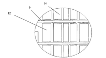
- Figure 2 is a partial enlarged view of a portion A in Figure 1;
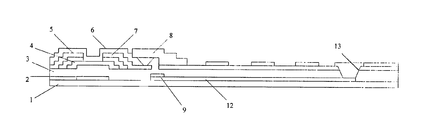
- FIG. 3 is a cross-sectional view of a third electrode of a substrate of a touch display screen according to an embodiment of the present invention.
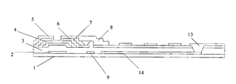
- FIG. 4 is a cross-sectional view of a second electrode of a substrate of a touch display screen according to an embodiment of the present invention
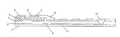
- FIG. 5 is a cross-sectional view of a first electrode of a substrate of a touch display screen according to an embodiment of the present invention.
- the embodiment of the invention provides a substrate for a touch display screen, a manufacturing method thereof, a touch screen and a display device.
- the touch emitter electrode and the touch receiving electrode are respectively shared with the common electrode, thereby making the touch
- the emitter electrode and the touch receiving electrode are disposed in the same layer, which simplifies the number of layers of the substrate during fabrication, thereby simplifying the structure of the substrate and reducing the cost of the touch screen.
- FIG. 1 is a top view of a substrate of a touch display screen according to an embodiment of the present invention
- FIG. 2 is a partial enlarged view of a portion of FIG.
- Embodiments of the present invention provide a substrate for a touch display screen, the substrate including a substrate 1 and an electrode layer disposed on the substrate 1, the electrode layer including a plurality of first and second electrical interconnects Electrode 10 and a plurality of third electrodes 11;
- the first electrode 10 and the third electrode 11 When the first electrode 10 and the third electrode 11 are in a first period of time of displaying a picture, the first electrode 10 and the third electrode 11 input a common electrode signal;
- the third electrode 11 and the first electrode 10 are in a part of the second period of time Part of the input touch signal.
- the electrode is disposed on the substrate, and the first electrode 10 serves as a common electrode and the touch receiving electrode, the third electrode 11 serves as a common electrode and a touch transmitting electrode, and is connected through the connecting line 9 and the electrode.
- the layer 13 forms a coupling capacitor, and the first electrode 10 and the third electrode 11 are driven in a time-sharing manner during driving, so that the touch receiving electrode and the touch transmitting electrode can be disposed in the same layer.
- the touch emitter electrode and the touch receiving electrode can be formed on the formed common electrode. Simplifies the structure of the substrate, reduces the production process of the substrate, and The manufacturing cost of the substrate is reduced.
- the capacitance of the coupling capacitance formed between the contact electrode connection layer 13 and the touch receiving electrode is affected, so that the coupling capacitance of the operator touch is different from the capacitance of the coupling capacitance at other positions, and the touch screen is The position of the coupling capacitor whose capacitance has changed is determined to determine the position touched by the operator.
- the substrate may be an array substrate or a color filter substrate.
- the substrate is an array substrate.
- each of the thin film transistor structures on the substrate is specifically: a gate electrode 2 disposed on the substrate 1; a gate insulating layer 3 disposed on the gate electrode 2; and the gate insulating layer 3 is disposed on the gate insulating layer 3
- each of the thin film transistors further includes a protective layer 6 disposed on the gate 2 and the drain 7. Thereby better protecting the structure on the substrate. Avoid damage to the structure on the substrate during fabrication.
- FIG. 1 In order to facilitate the understanding of the substrate provided by the embodiment of the present invention, the structure will be described in detail below with reference to FIG. 1, FIG. 2, FIG. 3, FIG. 4 and FIG.
- the number of the first electrodes 10 is plural, and the plurality of first electrodes 10 are arranged in parallel, and each of the first electrodes 10 is divided into a plurality of electrode segments by the third electrodes 11;
- the electrode segments of the first electrodes 10 are integrally connected by the electrode connection layers 13 disposed in different layers, and the projection of the electrode connection layer 13 on the substrate 1 intersects with the third electrodes 11.
- the electrode connection layer 13 is disposed in the same layer as the pixel electrode 8. Specifically, the pixel electrode 8 and the electrode connection layer 13 are disposed on the protective layer 9. At the time of fabrication, the pixel electrode 8 and the electrode connection layer 13 are simultaneously formed, and no additional fabrication process is required, which facilitates the fabrication of the substrate.
- the third electrode 11 includes a plurality of electrode segments, and any two adjacent electrode segments of the third electrode 11 are respectively located at two sides of the first electrode 10, and Adjacent electrode segments are connected to each other by a connection line 9 on which a projection of the electrode connection layer 13 intersects the connection line 9.
- a connection line 9 on which a projection of the electrode connection layer 13 intersects the connection line 9.
- FIG. 2 it can be seen from FIG. 2 that there is a gap between the connecting line 9 and the first electrode 10, thereby ensuring electrical isolation between the first electrode 10 and the third electrode 11.
- the electrode segments of the first electrode 10 and the electrode segments of the third electrode 11 are formed on the substrate 1.
- connection line 9 is formed, that is, the gate electrode 2 is disposed in the same layer as the connection line 9, and the material of the connection line 9 is the same as that of the gate electrode 2. Therefore, an additional process is not required to fabricate the connecting wires 9, which simplifies the method of fabricating the substrate.
- the width of the connecting line 9 ranges from 2 to 15 ⁇ m.
- the first electrode 10 includes a second electrode 12 and a fourth electrode 14 disposed in parallel, and the plurality of second electrodes 12 and the plurality of fourth electrodes 14 are spaced apart, and the plurality of second electrodes 12 inputs a common electrode signal, and the plurality of fourth electrodes 14 input a touch signal during the second period of time, that is, the second electrode 12 is a common electrode, and each of the second electrodes 12 is
- the third electrode 11 is partitioned into a plurality of electrode segments; the electrode segments of each of the second electrodes 12 are integrally connected by the electrode connection layer 13.
- the second electrode 12 serves as a pure common electrode.
- three kinds of electrodes are disposed on the substrate 1, and one is a fourth electrode 14, which can serve as both a common electrode and a touch receiving electrode, and the second type is The second electrode 12 serves as a common electrode, and the third is a third electrode 11, which can serve as both a common electrode and a touch emitter electrode.
- the first electrode 10 and the third electrode 11 are made of a transparent electrode material, that is, the electrode segments of the first electrode 10 and the electrode segments of the third electrode are transparent electrode segments. .
- the electrode connection layer 13 provided on the substrate is placed on the protective layer 6 at the time of substrate fabrication.
- the protective layer 13 is provided with a through hole through which the electrode connection layer is connected to the plurality of electrode segments of the first electrode.
- the first type of via holes are electrodes for connecting the common electrode and the touch emitter electrode (the third electrode) a through hole of 11), a through hole for connecting an electrode (fourth electrode 14) shared by the common electrode and the touch receiving electrode, and a third type of through hole for connecting the common electrode used separately (No. The through hole of the two electrodes 12).
- the electrode connection layer 13 connects the respective electrode segments of the fourth electrode 14, and connects the respective electrode segments of the second electrode 12, and connects the adjacent third electrodes 11.
- the invention also provides a method for manufacturing a substrate of a touch display screen, the method comprising the following steps:
- An electrode layer is formed on the substrate by a patterning process, the electrode layer including a first electrode 10 and a third electrode 11, and the first electrode 10 and the third electrode 11 are crossed and electrically insulated.
- the thin film transistor formed on the substrate 1 is specifically: an electrode segment in which a plurality of first electrodes disposed in parallel are etched in the formed electrode layer by one patterning process, and an electrode segment of the third electrode crossing the first electrode ;
- a connection line connecting the electrode segments of the third electrode is formed by one patterning process; specifically, a connection line of the gate electrode and the electrode segment connecting the third electrode is formed by one patterning process.
- a protective layer is formed on the formed thin film transistor before the electrode connection layer is formed, and a via hole corresponding to the electrode segment of the first electrode is formed in the protective layer.
- FIGS. 3, 4 and 5 are cross-sectional views of a third electrode of a substrate of a touch display screen according to an embodiment of the present invention.
- FIG. 4 is a cross-sectional view of a second electrode of a substrate of the touch display screen according to an embodiment of the present invention;
- Step 1 providing a TFT substrate, depositing an ITO layer on the surface of the TFT substrate, and patterning by photolithography to form: a second electrode 12 (common electrode Vcom), and a fourth electrode 14 (common electrode/touch receiving electrode Vcom/Rx) And the first electrode 11 (common electrode / touch transmitting electrode Vcom / Tx).
- a second electrode 12 common electrode Vcom
- a fourth electrode 14 common electrode/touch receiving electrode Vcom/Rx
- the first electrode 11 common electrode / touch transmitting electrode Vcom / Tx.
- Step 2 depositing a metal layer thereon, and patterning by photolithography to form a gate 2 (Gate), a connection line 9 (Tx), and the connection line 9 (Tx) overlaps the previously formed third electrode 11 (Vcom / Tx), and a certain gap between the second electrode (Vcom) and the fourth electrode 14 (Vcom / Rx).
- step 3 a gate insulating layer (GI) is deposited on the formed gate 2.
- GI gate insulating layer
- Step 4 depositing a semiconductor layer (ie, active layer 4) on the gate insulating layer 3, and the semiconductor layer can be divided into An amorphous silicon layer (Active) and a lightly doped amorphous silicon layer (n+), and then a second metal layer (SD) is deposited thereon, and the semiconductor layer and the second metal layer are patterned by photolithography to form a thin film Transistor channel, source 5 (S), drain 7 (D), data line (D).
- a semiconductor layer ie, active layer 4
- the semiconductor layer can be divided into An amorphous silicon layer (Active) and a lightly doped amorphous silicon layer (n+)
- SD second metal layer
- Step 5 depositing a protective layer 6 thereon, and patterning the protective layer 6 by photolithography, forming a connection hole of the pixel electrode 8, touching the emission connection hole, touching the receiving electrode connection hole, and the common electrode connection hole.
- step 6 an ITO layer is deposited thereon, and the pixel electrode 8 and the electrode connection layer 13 are patterned by photolithography.
- the embodiment of the invention further provides a touch screen, which comprises the substrate according to any one of the above.
- the electrode is disposed on the substrate, and the fourth electrode 14 serves as a common electrode and the touch receiving electrode, the third electrode 11 serves as a common electrode and a touch transmitting electrode, and is connected through the connecting line 9 and the electrode.
- the layer 13 forms a coupling capacitor, and the fourth electrode 14 and the third electrode 11 are driven in a time division manner during driving, so that the touch receiving electrode and the touch transmitting electrode can be disposed in the same layer.
- the touch emitter electrode and the touch receiving electrode can be formed on the formed common electrode.
- the structure of the substrate is simplified, the production process of the substrate is reduced, and the manufacturing cost of the substrate is reduced.
- the capacitance of the coupling capacitance formed between the contact electrode connection layer 13 and the touch receiving electrode is affected, so that the coupling capacitance of the operator touch is different from the capacitance of the coupling capacitance at other positions, and the touch screen is The position of the coupling capacitor whose capacitance has changed is determined to determine the position touched by the operator.
- the embodiment of the invention further provides a display device, which comprises the above touch screen.
- the electrode is disposed on the substrate, and the fourth electrode 14 serves as a common electrode and the touch receiving electrode, the third electrode 11 serves as a common electrode and a touch transmitting electrode, and is connected through the connecting line 9 and the electrode.
- the layer 13 forms a coupling capacitor, and the fourth electrode 14 and the third electrode 11 are driven in a time division manner during driving, so that the touch receiving electrode and the touch transmitting electrode can be disposed in the same layer.
- the touch emitter electrode and the touch receiving electrode can be formed on the formed common electrode. Simplifies the structure of the substrate, reduces the production process of the substrate, and The manufacturing cost of the substrate is reduced.
- the capacitance of the coupling capacitance formed between the electrode connection layer 13 and the touch receiving electrode is affected, so that the coupling capacitance of the touch at the operator is different from the capacitance of the coupling capacitance at other positions, and the touch screen is received according to the touch screen.
- the position of the coupling capacitor whose capacitance changes to determine the position touched by the operator.
Landscapes
- Physics & Mathematics (AREA)
- Engineering & Computer Science (AREA)
- Theoretical Computer Science (AREA)
- General Engineering & Computer Science (AREA)
- General Physics & Mathematics (AREA)
- Nonlinear Science (AREA)
- Human Computer Interaction (AREA)
- Mathematical Physics (AREA)
- Optics & Photonics (AREA)
- Crystallography & Structural Chemistry (AREA)
- Chemical & Material Sciences (AREA)
- Microelectronics & Electronic Packaging (AREA)
- Geometry (AREA)
- Devices For Indicating Variable Information By Combining Individual Elements (AREA)
- Position Input By Displaying (AREA)
Abstract
一种触摸显示屏的基板及其制造方法、触摸屏及显示装置。该基板包括衬底(1)和设置在衬底(1)上的一层电极层,电极层包括彼此交叉且电绝缘的多个第一电极(10)和多个第三电极(11);当第一电极(10)、第三电极(11)处于显示画面的第一时间段时,第一电极(10)、第三电极(11)输入公共电极信号;当第一电极(10)、第三电极(11)处于不显示画面的第二时间段时,第三电极(11)和第一电极(10)的一部分输入触控信号。触摸接收电极与触摸发射电极可以同层设置,在基板上形成公共电极时,即可在形成的公共电极上形成触摸发射电极及触摸接收电极。简化了基板的结构,减少了基板的生产工艺以及降低了基板的制作成本。
Description
本发明涉及到显示装置的技术领域,尤其涉及到一种触摸显示屏的基板及其制造方法、触摸屏及显示装置。
随着显示技术的飞速发展,触摸屏(Touch Screen Panel)已经逐渐遍及人们的生活中。目前,触摸屏按照工作原理可以分为:电阻式、电容式、红外线式以及表面声波式。其中,电容式触摸屏由于能够实现真正的多点控制和高灵敏度而成被业内广泛应用。
电容触摸屏按组成结构可分为:外挂式触摸屏、覆盖表面式触摸屏以及内嵌式触摸屏。其中,外挂式触摸屏是将触摸屏与显示屏分开生产,然后贴合到一起成为具有触摸功能的液晶显示屏,外挂式触摸屏存在制作成本高、光透过率较低、组模较厚等缺点。而内嵌式触摸屏将触摸屏的触控电极内嵌在液晶显示屏内部,可以减薄模组整体的厚度,又可以大大降低触摸屏的制作成本。因此,内嵌式触摸屏受到各大面板厂家青睐。
目前,现有技术的缺陷在于,现有电容屏采用分层设置的方式,即触摸发射电极及触摸接收电极分别设置在不同的层,从而造成触摸屏的结构比较复杂,增加了触摸基板的生产难度。
发明内容
本发明提供了一种触摸显示屏的基板、触摸屏及触摸屏,用以简化触摸屏的结构,降低触摸屏的成本。
本发明提供了一种触摸显示屏的基板,该基板包括衬底和设置在所述衬底
上的一层电极层,所述电极层包括多个第一电极和多个第三电极,所述第一电极和所述第三电极交叉且电绝缘设置;
当所述第一电极、第三电极处于显示画面的第一时间段时,所述第一电极、第三电极输入公共电极信号;
当所述第一电极、第三电极处于不显示画面的第二时间段时,所述第三电极和所述第一电极的一部分输入触控信号。
在上述技术方案中,通过在衬底上设置电极,并且其中的第一电极作为公共电极及触摸接收电极、第三电极作为公共电极及触摸发射电极,并且通过连接线及电极连接层形成耦合电容,在驱动时对第一电极及第三电极采用分时驱动,从而使得触摸接收电极与触摸发射电极可以同层设置。在制造时,在基板上形成公共电极后,即可在形成的公共电极上形成触摸发射电极及触摸接收电极。简化了基板的结构,减少了基板的生产工艺以及降低了基板的制作成本。
优选的,所述多个第一电极平行设置,每个第一电极被所述第三电极分隔成多个电极段;所述每个第一电极的电极段通过异层设置的电极连接层连接成一体,且所述电极连接层在所述衬底上的投影与所述第三电极交叉。
优选的,所述电极连接层与所述触摸显示屏的基板上的像素电极同层设置。
优选的,还包括设置在所述基板的薄膜晶体管上的保护层,所述电极连接层设置在所述保护层上。
优选的,所述保护层上设置有通孔,所述电极连接层穿过所述通孔与所述第一电极的多个电极段连接。
优选的,所述第三电极包括多个电极段,所述第三电极的任意相邻的两个电极段分别位于第一电极的两侧,且相邻的电极段之间通过连接线连接导通,所述电极连接层在所述衬底上的投影与所述连接线交叉。
优选的,所述连接线的材料与所述栅线的材料相同。
优选的,所述连接线的宽度范围在2-15μm。
优选的,所述第一电极及所述第二电极与所述基板的栅极同层设置。
优选的,所述第一电极的电极段及第三电极的电极段均为透明电极段。
优选的,所述多个第一电极还包括多个第二电极和多个第四电极,且所述多个第二电极和多个第四电极间隔设置,所述多个第二电极只输入公共电极信号,所述多个第四电极在所述第二时间段内输入触控信号。
本发明还提供了一种触摸屏的基板的制作方法,包括以下步骤:
通过构图工艺在衬底形成一层电极层,所述电极层包括的第一电极和第三电极,所述第一电极和所述第三电极交叉且电绝缘设置。
在上述技术方案中,通过在同一层上形成第一电极和第三电极,且第一电极和第三电极可以作为触控电极,在基板上形成公共电极时,即可在形成的公共电极上形成触摸发射电极及触摸接收电极。简化了基板的结构,减少了基板的生产工艺以及降低了基板的制作成本。
优选的,所述在衬底形成一层电极层,所述电极层包括的第一电极和第三电极,所述第一电极和所述第三电极交叉且电绝缘设置具体为:
通过一次构图工艺在形成的电极层刻蚀出多个平行设置的第一电极的电极段,及与第一电极交叉的第三电极的电极段;
通过一次构图工艺形成连接第三电极的电极段的连接线;
通过一次构图工艺形成电极连接层,且所述电极连接层在所述衬底上的投影与所述第三电极交叉。
优选的,通过一次构图工艺形成连接第三电极的电极段的连接线具体为:
通过一次构图工艺形成栅极和连接第三电极的电极段的连接线。
优选的,通过一次构图工艺形成电极连接层具体为:通过一次构图工艺形成像素电极和电极连接层,且所述电极连接层在所述衬底上的投影与所述第三电极交叉。
优选的,在形成电极连接层之前还包括:
在形成的薄膜晶体管上形成保护层,在保护层形成与所述第一电极的电极
段相对应的通孔。
本发明还提供了一种触摸屏,所述触摸屏包括上述任一项所述的基板。
在上述技术方案中,通过在衬底上设置电极,并且其中的第一电极作为公共电极及触摸接收电极、第三电极作为公共电极及触摸发射电极,并且通过连接线及电极连接层形成耦合电容,在驱动时对第一电极及第三电极采用分时驱动,从而使得触摸接收电极与触摸发射电极可以同层设置。在制造时,在基板上形成公共电极后,即可在形成的公共电极上形成触摸发射电极及触摸接收电极。简化了基板的结构,减少了基板的生产工艺以及降低了基板的制作成本。
本发明还提供了一种显示装置,该显示装置包括上述的触摸屏。
在上述技术方案中,通过在衬底上设置电极,并且其中的第一电极作为公共电极及触摸接收电极、第三电极作为公共电极及触摸发射电极,并且通过连接线及电极连接层形成耦合电容,在驱动时对第一电极及第三电极采用分时驱动,从而使得触摸接收电极与触摸发射电极可以同层设置。在制造时,在基板上形成公共电极后,即可在形成的公共电极上形成触摸发射电极及触摸接收电极。简化了基板的结构,减少了基板的生产工艺以及降低了基板的制作成本。
图1为本发明实施例提供的触摸显示屏的基板的俯视图;
图2为图1中A处的局部放大图;
图3为本发明实施例提供的触摸显示屏的基板的第三电极处的剖视图;
图4为本发明实施例提供的触摸显示屏的基板的第二电极处的剖视图;
图5为本发明实施例提供的触摸显示屏的基板的第一电极处的剖视图。
附图标记:
1-衬底 2-栅极 3-栅极绝缘层
4-有源层 5-源极 6-保护层
7-漏极 8-像素电极 9-连接线
10-第一电极 11-第三电极 12-第二电极
13-电极连接层 14-第四电极
为了简化触摸屏的结构,降低触摸屏的成本。本发明实施例提供了一种触摸显示屏的基板及其制造方法、触摸屏及显示装置,在本发明的技术方案中,通过采用将触摸发射电极及触摸接收电极分别与公共电极共用,从而使得触摸发射电极及触摸接收电极在同层设置,简化了基板在制作时层数,进而简化了基板的结构,降低了触摸屏的成本。为使本发明的目的、技术方案和优点更加清楚,以下举实施例对本发明作进一步详细说明。
如图1及图2所示,图1为本发明实施例提供的触摸显示屏的基板的俯视图;图2为图1中A处的局部放大图。
本发明实施例提供了一种触摸显示屏的基板,该基板包括衬底1和设置在所述衬底1上的一层电极层,所述电极层包括彼此交叉且电绝缘的多个第一电极10和多个第三电极11;
当所述第一电极10、第三电极11处于显示画面的第一时间段时,所述第一电极10、第三电极11输入公共电极信号;
当所述第一电极10、第三电极11处于不显示画面的第二时间段时,在所述第二时间段的部分时间段内,所述第三电极11和所述第一电极10的一部分输入触控信号。
在上述具体实施例中,通过在衬底上设置电极,并且其中的第一电极10作为公共电极及触摸接收电极、第三电极11作为公共电极及触摸发射电极,并且通过连接线9及电极连接层13形成耦合电容,在驱动时对第一电极10及第三电极11采用分时驱动,从而使得触摸接收电极与触摸发射电极可以同层设置。在制造时,在基板上形成公共电极后,即可在形成的公共电极上形成触摸发射电极及触摸接收电极。简化了基板的结构,减少了基板的生产工艺以及
降低了基板的制作成本。当操作者触摸到触摸屏时,影响到触电极连接层13与触摸接收电极之间形成的耦合电容的电容量,使操作者触摸处的耦合电容与其他位置的耦合电容的电容量不同,触摸屏根据接收到的电容量发生变化的耦合电容的位置来确定操作者触摸的位置。
此外,该基板既可以为阵列基板也可以作为彩膜基板,较佳的,该基板为阵列基板。并且该基板上的每个薄膜晶体管结构具体为:设置在所述衬底1上的栅极2;设置在所述栅极2上的栅极绝缘层3;设置在所述栅极绝缘层3上的有源层4;设置在所述有源层4上的源极5和漏极7。从而形成控制像素单元中的液晶层的液晶分子偏转的结构。更佳的,每个薄膜晶体管还包括设置在所述栅极2和漏极7上的保护层6。从而更好的保护基板上的结构。避免基板上的结构在制作时被损坏。
为了方便对本发明实施例提供的基板的理解,下面结合附图1、图2、图3、图4及图5对其结构进行详细的描述。
继续参考图1及图2,其中的第一电极10的个数为多个,且多个第一电极10平行设置,每个第一电极10被第三电极11分隔成多个电极段;每个第一电极10的电极段通过异层设置的电极连接层13连接成一体,且电极连接层13在衬底1上的投影与第三电极11交叉。其中的电极连接层13与像素电极8同层设置,具体的,该像素电极8及电极连接层13设置在保护层9上。且在制作时,像素电极8和电极连接层13同时形成,无需额外的制作工艺,方便了基板的制作。
继续参考图1,由图1可以看出,所述第三电极11包括多个电极段,所述第三电极11的任意相邻的两个电极段分别位于第一电极10的两侧,且相邻的电极段之间通过连接线9连接导通,所述电极连接层13在所述衬底1上的投影与所述连接线9交叉。一并参考图2,由图2中可以看出,连接线9与第一电极10之间存在间隙,从而保证了第一电极10和第三电极11之间电隔离。在具体制作时,第一电极10的电极段和第三电极11的电极段在衬底1上形成,
之后,在形成栅极2时,形成连接线9,即栅极2与连接线9同层设置,且连接线9的材料与所述栅极2的材料相同。从而无需额外的工序来制作连接线9,简化了基板的制作方法。在具体制作时,连接线9的宽度范围在2-15μm。
继续参考图1,上述第一电极10包括平行设置的第二电极12和第四电极14,且所述多个第二电极12和多个第四电极14间隔设置,所述多个第二电极12只输入公共电极信号,所述多个第四电极14在所述第二时间段内,输入触控信号,即所述第二电极12为公共电极,且每个第二电极12被所述第三电极11分隔成多个电极段;所述每个第二电极12的电极段通过所述电极连接层13连接成一体。该第二电极12作为纯粹的公共电极,此时,衬底1上设置了三种电极,一种为第四电极14,该电极既可以作为公共电极又可以作为触摸接收电极,第二种为第二电极12,该电极作为公共电极,第三种为第三电极11,该电极既可以作为公共电极又可以作为触摸发射电极。
一并参考图3、图4及图5,其中的,第一电极10和第三电极11采用透明电极材料制作,即第一电极10的电极段及第三电极的电极段均为透明电极段。
在基板制作时,该设置的电极连接层13位于保护层6之上。保护层13上设置有通孔,所述电极连接层穿过所述通孔与所述第一电极的多个电极段连接。具体的在制作时,在基板上形成的栅极绝缘层3及保护层6上形成三类通孔,其中第一类通孔是用于连通公共电极与触摸发射电极共用的电极(第三电极11)的通孔,另一类通孔是用于连通公共电极与触摸接收电极共用的电极(第四电极14)的通孔,第三类通孔是用于连通单独使用的公共电极(第二电极12)的通孔。在保护层6上形成电极连接层13时,电极连接层13将第四电极14的各个电极段连通,以及将第二电极12的各个电极段连接,以及将相邻的第三电极11连通。
为了方便对本发明实施例的理解,下面结合其制作方法对其进行详细的说明。
本发明还提供了一种触摸显示屏的基板的制作方法,该方法包括以下步骤:
通过构图工艺在衬底形成一层电极层,所述电极层包括的第一电极10和第三电极11,所述第一电极10和所述第三电极11交叉且电绝缘设置。
其中的在衬底1上形成薄膜晶体管具体为:通过一次构图工艺在形成的电极层刻蚀出多个平行设置的第一电极的电极段,及与第一电极交叉的第三电极的电极段;
通过一次构图工艺形成连接第三电极的电极段的连接线;具体的,通过一次构图工艺形成栅极和连接第三电极的电极段的连接线。
通过一次构图工艺形成电极连接层,且所述电极连接层在所述衬底上的投影与所述第三电极交叉;具体的,通过一次构图工艺形成像素电极和电极连接层,且所述电极连接层在所述衬底上的投影与所述第三电极交叉。
此外,还包括在形成电极连接层之前,在形成的薄膜晶体管上形成保护层,在保护层形成与所述第一电极的电极段相对应的通孔。
为了方便理解,下面结合附图3、图4及图5进行详细说明。其中,图3为本发明实施例提供的触摸显示屏的基板的第三电极处的剖视图;图4为本发明实施例提供的触摸显示屏的基板的第二电极处的剖视图;图5为本发明实施例提供的触摸显示屏的基板的第一电极处的剖视图。
步骤1,提供TFT基板,在TFT基板表面沉积ITO层,并利用光刻技术图案化,形成:第二电极12(公共电极Vcom),第四电极14(公共电极/触摸接收电极Vcom/Rx),和第一电极11(公共电极/触摸发射电极Vcom/Tx)。
步骤2,在其上沉积金属层,并利用光刻技术图案化,形成栅极2(Gate),连接线9(Tx),且该连接线9(Tx)搭接在之前形成的第三电极11(Vcom/Tx)上,并与第二电极(Vcom)及第四电极14(Vcom/Rx)之间间隔一定的间隙。
步骤3,在形成的栅极2上沉积栅绝缘层(GI)。
步骤4,在栅极绝缘层3上沉积半导体层(即有源层4),半导体层可分为
非晶硅层(Active)和轻掺杂的非晶硅层(n+),再在其上沉积第二金属层(SD),并利用光刻技术图案化半导体层和第二金属层,形成薄膜晶体管沟道,源极5(S),漏极7(D),数据线(D)。
步骤5,在其上沉积保护层6,并利用光刻技术图案化保护层6,形成像素电极8连接孔,触摸发射连接孔,触摸接收电极连接孔,公共电极连接孔。
步骤6,在其上沉积ITO层,并利用光刻技术图案化像素电极8和电极连接层13。
本发明实施例还提供了一种触摸屏,所述触摸屏包括上述任一项所述的基板。
在上述具体实施例中,通过在衬底上设置电极,并且其中的第四电极14作为公共电极及触摸接收电极、第三电极11作为公共电极及触摸发射电极,并且通过连接线9及电极连接层13形成耦合电容,在驱动时对第四电极14及第三电极11采用分时驱动,从而使得触摸接收电极与触摸发射电极可以同层设置。在制造时,在基板上形成公共电极后,即可在形成的公共电极上形成触摸发射电极及触摸接收电极。简化了基板的结构,减少了基板的生产工艺以及降低了基板的制作成本。当操作者触摸到触摸屏时,影响到触电极连接层13与触摸接收电极之间形成的耦合电容的电容量,使操作者触摸处的耦合电容与其他位置的耦合电容的电容量不同,触摸屏根据接收到的电容量发生变化的耦合电容的位置来确定操作者触摸的位置。
本发明实施例还提供了一种显示装置,该显示装置包括上述的触摸屏。
在上述具体实施例中,通过在衬底上设置电极,并且其中的第四电极14作为公共电极及触摸接收电极、第三电极11作为公共电极及触摸发射电极,并且通过连接线9及电极连接层13形成耦合电容,在驱动时对第四电极14及第三电极11采用分时驱动,从而使得触摸接收电极与触摸发射电极可以同层设置。在制造时,在基板上形成公共电极后,即可在形成的公共电极上形成触摸发射电极及触摸接收电极。简化了基板的结构,减少了基板的生产工艺以及
降低了基板的制作成本。当操作者触摸到触摸屏时,影响到电极连接层13与触摸接收电极之间形成的耦合电容的电容量,使操作者触摸处的耦合电容与其他位置的耦合电容的电容量不同,触摸屏根据接收到的电容量发生变化的耦合电容的位置来确定操作者触摸的位置。
显然,本领域的技术人员可以对本发明进行各种改动和变型而不脱离本发明的精神和范围。这样,倘若本发明的这些修改和变型属于本发明权利要求及其等同技术的范围之内,则本发明也意图包含这些改动和变型在内。
Claims (18)
- 一种触摸显示屏的基板,其特征在于,该基板包括衬底和设置在所述衬底上的一层电极层,所述电极层包括彼此交叉且电绝缘的多个第一电极和多个第三电极;当所述第一电极、第三电极处于显示画面的第一时间段时,所述第一电极、第三电极输入公共电极信号;当所述第一电极、第三电极处于不显示画面的第二时间段时,所述第三电极和所述第一电极的一部分输入触控信号。
- 如权利要求1所述的触摸显示屏的基板,其特征在于,所述多个第一电极平行设置,每个第一电极被所述第三电极分隔成多个电极段;所述每个第一电极的电极段通过与所述第一电极异层设置的电极连接层连接成一体,且所述电极连接层在所述衬底上的投影与所述第三电极交叉。
- 如权利要求2所述的触摸显示屏的基板,其特征在于,所述电极连接层与所述触摸显示屏的基板上的像素电极同层设置。
- 如权利要求3所述的触摸显示屏的基板,其特征在于,还包括设置在所述基板的薄膜晶体管上的保护层,所述电极连接层设置在所述保护层上。
- [根据细则26改正29.12.2015]
如权利要求4所述的触摸显示屏的基板,其特征在于,所述保护层上设置有通孔,所述电极连接层穿过所述通孔与所述第一电极的多个电极段连接。 - [根据细则26改正29.12.2015]
如权利要求2所述的触摸显示屏的基板,其特征在于,所述第三电极包括多个电极段,所述第三电极的任意相邻的两个电极段分别位于第一电极的两侧,且相邻的电极段之间通过连接线连接导通,所述电极连接层在所述衬底上的投影与所述连接线交叉。 - [根据细则26改正29.12.2015]
如权利要求6所述的触摸显示屏的基板,其特征在于,所述连接线的材料与所述栅线的材料相同。 - [根据细则26改正29.12.2015]
如权利要求6所述的触摸显示屏的基板,其特征在于,所述连接线的 宽度范围在2-15μm。 - [根据细则26改正29.12.2015]
如权利要求1~8任一项所述的触摸显示屏的基板,其特征在于,所述第一电极及所述第二电极与所述基板的栅极同层设置。 - [根据细则26改正29.12.2015]
如权利要求9所述的触摸显示屏的基板,其特征在于,所述第一电极的电极段及第三电极的电极段均为透明电极段。 - [根据细则26改正29.12.2015]
如权利要求9所述的基板,其特征在于,所述多个第一电极还包括多个第二电极和多个第四电极,且所述多个第二电极和多个第四电极间隔设置,所述多个第二电极只输入公共电极信号,所述多个第四电极在所述第二时间段内输入触控信号。 - [根据细则26改正29.12.2015]
一种触摸显示屏的基板的制作方法,其特征在于,包括以下步骤:通过构图工艺在衬底上形成一层电极层,所述电极层包括第一电极和第三电极,所述第一电极和所述第三电极交叉且电绝缘设置。 - [根据细则26改正29.12.2015]
如权利要求12所述的制作方法,其特征在于,所述在衬底上形成一层电极层,所述电极层包括第一电极和第三电极,所述第一电极和所述第三电极交叉且电绝缘设置的步骤具体包括:通过一次构图工艺在形成的电极层刻蚀出多个平行设置的第一电极的电极段,及与第一电极交叉的第三电极的电极段;通过一次构图工艺形成连接第三电极的电极段的连接线;通过一次构图工艺形成电极连接层,且所述电极连接层在所述衬底上的投影与所述第三电极交叉。 - [根据细则26改正29.12.2015]
如权利要求13所述的制作方法,其特征在于,通过一次构图工艺形成连接第三电极的电极段的连接线具体为:通过一次构图工艺形成栅极和连接第三电极的电极段的连接线。 - [根据细则26改正29.12.2015]
如权利要求13所述的制作方法,其特征在于,通过一次构图工艺形成电极连接层具体为:通过一次构图工艺形成像素电极和电极连接层,且所述电极连接层在所述衬底上的投影与所述第三电极交叉。 - [根据细则26改正29.12.2015]
如权利要求13所述的制作方法,其特征在于,在形成电极连接层之前还包括:在形成的薄膜晶体管上形成保护层,在保护层中形成与所述第一电极的电极段相对应的通孔。 - [根据细则26改正29.12.2015]
一种触摸屏,其特征在于,所述触摸屏包括如权利要求1~12任一项所述的基板。 - [根据细则26改正29.12.2015]
一种显示装置,其特征在于,包括如权利要求18所述的触摸屏。
Priority Applications (2)
| Application Number | Priority Date | Filing Date | Title |
|---|---|---|---|
| EP15874991.1A EP3242191B1 (en) | 2014-12-31 | 2015-11-17 | Substrate of touch display screen and manufacturing method therefor, touch screen and display device |
| US15/325,146 US9927647B2 (en) | 2014-12-31 | 2015-11-17 | Substrate of touch display screen and method of fabricating the same, touch screen and display device |
Applications Claiming Priority (2)
| Application Number | Priority Date | Filing Date | Title |
|---|---|---|---|
| CN201410855010.3 | 2014-12-31 | ||
| CN201410855010.3A CN104503647B (zh) | 2014-12-31 | 2014-12-31 | 一种触摸显示屏的基板及其制造方法、触摸屏及显示装置 |
Publications (1)
| Publication Number | Publication Date |
|---|---|
| WO2016107310A1 true WO2016107310A1 (zh) | 2016-07-07 |
Family
ID=52945048
Family Applications (1)
| Application Number | Title | Priority Date | Filing Date |
|---|---|---|---|
| PCT/CN2015/094752 Ceased WO2016107310A1 (zh) | 2014-12-31 | 2015-11-17 | 一种触摸显示屏的基板及其制造方法、触摸屏及显示装置 |
Country Status (4)
| Country | Link |
|---|---|
| US (1) | US9927647B2 (zh) |
| EP (1) | EP3242191B1 (zh) |
| CN (1) | CN104503647B (zh) |
| WO (1) | WO2016107310A1 (zh) |
Families Citing this family (5)
| Publication number | Priority date | Publication date | Assignee | Title |
|---|---|---|---|---|
| CN104503647B (zh) | 2014-12-31 | 2017-12-08 | 京东方科技集团股份有限公司 | 一种触摸显示屏的基板及其制造方法、触摸屏及显示装置 |
| CN104915054B (zh) | 2015-05-14 | 2019-10-15 | 京东方科技集团股份有限公司 | 阵列基板及其制作方法和显示装置 |
| US10684500B2 (en) | 2015-05-27 | 2020-06-16 | Semiconductor Energy Laboratory Co., Ltd. | Touch panel |
| CN105629545A (zh) * | 2016-01-19 | 2016-06-01 | 深圳市华星光电技术有限公司 | 触摸面板以及其制造方法 |
| CN110187787A (zh) * | 2018-02-22 | 2019-08-30 | 蓝思科技(长沙)有限公司 | 一种触控屏边框 |
Citations (7)
| Publication number | Priority date | Publication date | Assignee | Title |
|---|---|---|---|---|
| CN102841717A (zh) * | 2012-08-31 | 2012-12-26 | 北京京东方光电科技有限公司 | 一种电容式触摸屏及其制造方法 |
| CN103955320A (zh) * | 2014-04-21 | 2014-07-30 | 合肥鑫晟光电科技有限公司 | 触摸基板及触摸屏 |
| US20140267950A1 (en) * | 2013-03-12 | 2014-09-18 | Samsung Display Co., Ltd. | Flexible display device with flexible touch screen panel |
| CN104199580A (zh) * | 2014-08-29 | 2014-12-10 | 合肥鑫晟光电科技有限公司 | 一种触摸屏、其制作方法及触摸显示装置 |
| CN104216578A (zh) * | 2013-05-30 | 2014-12-17 | 京东方科技集团股份有限公司 | 一种触摸面板及显示装置 |
| CN104503647A (zh) * | 2014-12-31 | 2015-04-08 | 京东方科技集团股份有限公司 | 一种触摸显示屏的基板及其制造方法、触摸屏及显示装置 |
| CN204515743U (zh) * | 2014-12-31 | 2015-07-29 | 京东方科技集团股份有限公司 | 一种触摸显示屏的基板、触摸屏及显示装置 |
Family Cites Families (16)
| Publication number | Priority date | Publication date | Assignee | Title |
|---|---|---|---|---|
| KR101284714B1 (ko) * | 2010-09-20 | 2013-07-17 | 엘지디스플레이 주식회사 | 액정 표시장치와 이의 제조방법 |
| KR101273239B1 (ko) * | 2010-09-20 | 2013-06-11 | 엘지디스플레이 주식회사 | 터치 스크린이 내장된 액정 표시장치와 이의 제조방법 |
| CN103135815B (zh) * | 2011-11-25 | 2017-02-22 | 上海天马微电子有限公司 | 内嵌触摸屏液晶显示装置及其触控驱动方法 |
| KR101353284B1 (ko) * | 2012-04-25 | 2014-01-21 | 엘지디스플레이 주식회사 | 액정 디스플레이 장치와 이의 제조방법 |
| TWI464643B (zh) * | 2012-05-25 | 2014-12-11 | J Touch Corp | 偏光片之觸控感應元件製作方法與偏光裝置 |
| CN103092452B (zh) * | 2013-01-28 | 2016-03-23 | 北京京东方光电科技有限公司 | 电容触摸屏及其制作方法和触摸显示装置 |
| CN103150070B (zh) * | 2013-03-05 | 2016-07-06 | 合肥京东方光电科技有限公司 | 一种电容式触控模组、电容式内嵌触摸屏及显示装置 |
| CN203117953U (zh) * | 2013-03-05 | 2013-08-07 | 合肥京东方光电科技有限公司 | 一种电容式触控模组、电容式内嵌触摸屏及显示装置 |
| CN203376696U (zh) * | 2013-06-06 | 2014-01-01 | 敦泰科技有限公司 | 触控显示装置 |
| KR102092569B1 (ko) * | 2013-09-17 | 2020-03-25 | 엘지디스플레이 주식회사 | 터치 스크린 일체형 디스플레이 장치와 이의 구동 방법 |
| CN103699284B (zh) * | 2013-12-27 | 2016-09-21 | 京东方科技集团股份有限公司 | 一种电容式内嵌触摸屏及其制备方法、显示装置 |
| CN103885637B (zh) * | 2014-03-12 | 2017-05-31 | 京东方科技集团股份有限公司 | 一种内嵌式触摸屏及显示装置 |
| CN104035640B (zh) * | 2014-05-30 | 2017-10-27 | 京东方科技集团股份有限公司 | 一种内嵌式触摸屏及显示装置 |
| CN104020891A (zh) * | 2014-05-30 | 2014-09-03 | 京东方科技集团股份有限公司 | 一种内嵌式触摸屏及显示装置 |
| CN104216564B (zh) * | 2014-09-01 | 2017-09-01 | 上海天马微电子有限公司 | 一种触摸屏、触摸显示面板及显示装置 |
| CN104238854B (zh) * | 2014-09-10 | 2018-01-02 | 京东方科技集团股份有限公司 | 一种阵列基板和具有该阵列基板的电容式内嵌触摸屏 |
-
2014
- 2014-12-31 CN CN201410855010.3A patent/CN104503647B/zh active Active
-
2015
- 2015-11-17 US US15/325,146 patent/US9927647B2/en active Active
- 2015-11-17 WO PCT/CN2015/094752 patent/WO2016107310A1/zh not_active Ceased
- 2015-11-17 EP EP15874991.1A patent/EP3242191B1/en active Active
Patent Citations (7)
| Publication number | Priority date | Publication date | Assignee | Title |
|---|---|---|---|---|
| CN102841717A (zh) * | 2012-08-31 | 2012-12-26 | 北京京东方光电科技有限公司 | 一种电容式触摸屏及其制造方法 |
| US20140267950A1 (en) * | 2013-03-12 | 2014-09-18 | Samsung Display Co., Ltd. | Flexible display device with flexible touch screen panel |
| CN104216578A (zh) * | 2013-05-30 | 2014-12-17 | 京东方科技集团股份有限公司 | 一种触摸面板及显示装置 |
| CN103955320A (zh) * | 2014-04-21 | 2014-07-30 | 合肥鑫晟光电科技有限公司 | 触摸基板及触摸屏 |
| CN104199580A (zh) * | 2014-08-29 | 2014-12-10 | 合肥鑫晟光电科技有限公司 | 一种触摸屏、其制作方法及触摸显示装置 |
| CN104503647A (zh) * | 2014-12-31 | 2015-04-08 | 京东方科技集团股份有限公司 | 一种触摸显示屏的基板及其制造方法、触摸屏及显示装置 |
| CN204515743U (zh) * | 2014-12-31 | 2015-07-29 | 京东方科技集团股份有限公司 | 一种触摸显示屏的基板、触摸屏及显示装置 |
Non-Patent Citations (1)
| Title |
|---|
| See also references of EP3242191A4 * |
Also Published As
| Publication number | Publication date |
|---|---|
| EP3242191B1 (en) | 2020-05-27 |
| CN104503647A (zh) | 2015-04-08 |
| EP3242191A1 (en) | 2017-11-08 |
| US20170184896A1 (en) | 2017-06-29 |
| US9927647B2 (en) | 2018-03-27 |
| EP3242191A4 (en) | 2018-08-01 |
| CN104503647B (zh) | 2017-12-08 |
Similar Documents
| Publication | Publication Date | Title |
|---|---|---|
| KR102559090B1 (ko) | 인셀형 터치 패널을 갖는 백플레인 기판 | |
| JP5073467B2 (ja) | 液晶表示装置及びその製造方法 | |
| CN104597670B (zh) | 一种阵列基板及其制作方法及显示装置 | |
| CN105739739B (zh) | 内嵌触摸液晶显示设备及其制造方法 | |
| CN103885223B (zh) | 一种触控显示面板、触控显示装置 | |
| CN108227326A (zh) | 阵列基板及其制造方法、触控显示面板 | |
| WO2017004986A1 (zh) | 触控显示面板及其制作方法、触控显示装置 | |
| CN107589576B (zh) | 阵列基板及其制作方法、触控显示面板 | |
| WO2017197934A1 (zh) | 阵列基板及其制作方法、触控显示装置 | |
| WO2015106538A1 (zh) | 触控显示面板及其制备方法 | |
| CN106354347A (zh) | 内嵌式触控显示面板以及其制作方法 | |
| WO2016201838A1 (zh) | 触控面板及其制备方法、触控显示装置 | |
| WO2016119373A1 (zh) | 阵列基板、触控面板及阵列基板的制作方法 | |
| WO2017008450A1 (zh) | 平面转换模式阵列基板及其制作方法、显示器件 | |
| WO2016192121A1 (zh) | 自电容式内嵌触摸屏及其制备方法、液晶显示器 | |
| CN104460163B (zh) | 一种阵列基板及其制作方法及显示装置 | |
| WO2015010421A1 (zh) | 阵列基板、内嵌式触摸屏及显示装置 | |
| CN205375436U (zh) | 阵列基板、触控显示面板及触控显示装置 | |
| WO2013139192A1 (zh) | 触摸液晶显示装置、液晶显示面板及上部基板 | |
| CN113260958B (zh) | 阵列基板及其驱动方法、触控显示装置 | |
| WO2016107310A1 (zh) | 一种触摸显示屏的基板及其制造方法、触摸屏及显示装置 | |
| WO2014173024A1 (zh) | 阵列基板及其制作方法、显示装置 | |
| CN105974637A (zh) | 阵列基板及其制作方法、显示装置及其触摸位置检测方法 | |
| WO2018119788A1 (zh) | 内嵌触摸结构的阵列基板以及显示面板 | |
| CN105655348B (zh) | 一种阵列基板及其制作方法、显示面板和显示装置 |
Legal Events
| Date | Code | Title | Description |
|---|---|---|---|
| 121 | Ep: the epo has been informed by wipo that ep was designated in this application |
Ref document number: 15874991 Country of ref document: EP Kind code of ref document: A1 |
|
| WWE | Wipo information: entry into national phase |
Ref document number: 15325146 Country of ref document: US |
|
| REEP | Request for entry into the european phase |
Ref document number: 2015874991 Country of ref document: EP |
|
| NENP | Non-entry into the national phase |
Ref country code: DE |