WO2016111098A1 - センサシステムおよびデバイス - Google Patents
センサシステムおよびデバイス Download PDFInfo
- Publication number
- WO2016111098A1 WO2016111098A1 PCT/JP2015/083889 JP2015083889W WO2016111098A1 WO 2016111098 A1 WO2016111098 A1 WO 2016111098A1 JP 2015083889 W JP2015083889 W JP 2015083889W WO 2016111098 A1 WO2016111098 A1 WO 2016111098A1
- Authority
- WO
- WIPO (PCT)
- Prior art keywords
- fet
- sensor
- well
- source
- potential
- Prior art date
- Legal status (The legal status is an assumption and is not a legal conclusion. Google has not performed a legal analysis and makes no representation as to the accuracy of the status listed.)
- Ceased
Links
Images












Classifications
-
- G—PHYSICS
- G01—MEASURING; TESTING
- G01N—INVESTIGATING OR ANALYSING MATERIALS BY DETERMINING THEIR CHEMICAL OR PHYSICAL PROPERTIES
- G01N27/00—Investigating or analysing materials by the use of electric, electrochemical, or magnetic means
- G01N27/26—Investigating or analysing materials by the use of electric, electrochemical, or magnetic means by investigating electrochemical variables; by using electrolysis or electrophoresis
- G01N27/403—Cells and electrode assemblies
- G01N27/414—Ion-sensitive or chemical field-effect transistors, i.e. ISFETS or CHEMFETS
- G01N27/4141—Ion-sensitive or chemical field-effect transistors, i.e. ISFETS or CHEMFETS specially adapted for gases
-
- G—PHYSICS
- G01—MEASURING; TESTING
- G01K—MEASURING TEMPERATURE; MEASURING QUANTITY OF HEAT; THERMALLY-SENSITIVE ELEMENTS NOT OTHERWISE PROVIDED FOR
- G01K7/00—Measuring temperature based on the use of electric or magnetic elements directly sensitive to heat ; Power supply therefor, e.g. using thermoelectric elements
- G01K7/01—Measuring temperature based on the use of electric or magnetic elements directly sensitive to heat ; Power supply therefor, e.g. using thermoelectric elements using semiconducting elements having PN junctions
-
- G—PHYSICS
- G01—MEASURING; TESTING
- G01K—MEASURING TEMPERATURE; MEASURING QUANTITY OF HEAT; THERMALLY-SENSITIVE ELEMENTS NOT OTHERWISE PROVIDED FOR
- G01K7/00—Measuring temperature based on the use of electric or magnetic elements directly sensitive to heat ; Power supply therefor, e.g. using thermoelectric elements
- G01K7/01—Measuring temperature based on the use of electric or magnetic elements directly sensitive to heat ; Power supply therefor, e.g. using thermoelectric elements using semiconducting elements having PN junctions
- G01K7/015—Measuring temperature based on the use of electric or magnetic elements directly sensitive to heat ; Power supply therefor, e.g. using thermoelectric elements using semiconducting elements having PN junctions using microstructures, e.g. made of silicon
-
- G—PHYSICS
- G01—MEASURING; TESTING
- G01K—MEASURING TEMPERATURE; MEASURING QUANTITY OF HEAT; THERMALLY-SENSITIVE ELEMENTS NOT OTHERWISE PROVIDED FOR
- G01K7/00—Measuring temperature based on the use of electric or magnetic elements directly sensitive to heat ; Power supply therefor, e.g. using thermoelectric elements
- G01K7/16—Measuring temperature based on the use of electric or magnetic elements directly sensitive to heat ; Power supply therefor, e.g. using thermoelectric elements using resistive elements
- G01K7/22—Measuring temperature based on the use of electric or magnetic elements directly sensitive to heat ; Power supply therefor, e.g. using thermoelectric elements using resistive elements the element being a non-linear resistance, e.g. thermistor
- G01K7/226—Measuring temperature based on the use of electric or magnetic elements directly sensitive to heat ; Power supply therefor, e.g. using thermoelectric elements using resistive elements the element being a non-linear resistance, e.g. thermistor using microstructures, e.g. silicon spreading resistance
-
- G—PHYSICS
- G01—MEASURING; TESTING
- G01N—INVESTIGATING OR ANALYSING MATERIALS BY DETERMINING THEIR CHEMICAL OR PHYSICAL PROPERTIES
- G01N27/00—Investigating or analysing materials by the use of electric, electrochemical, or magnetic means
-
- G—PHYSICS
- G01—MEASURING; TESTING
- G01N—INVESTIGATING OR ANALYSING MATERIALS BY DETERMINING THEIR CHEMICAL OR PHYSICAL PROPERTIES
- G01N27/00—Investigating or analysing materials by the use of electric, electrochemical, or magnetic means
- G01N27/26—Investigating or analysing materials by the use of electric, electrochemical, or magnetic means by investigating electrochemical variables; by using electrolysis or electrophoresis
- G01N27/403—Cells and electrode assemblies
- G01N27/414—Ion-sensitive or chemical field-effect transistors, i.e. ISFETS or CHEMFETS
- G01N27/4148—Integrated circuits therefor, e.g. fabricated by CMOS processing
-
- G—PHYSICS
- G01—MEASURING; TESTING
- G01N—INVESTIGATING OR ANALYSING MATERIALS BY DETERMINING THEIR CHEMICAL OR PHYSICAL PROPERTIES
- G01N33/00—Investigating or analysing materials by specific methods not covered by groups G01N1/00 - G01N31/00
- G01N33/0004—Gaseous mixtures, e.g. polluted air
- G01N33/0009—General constructional details of gas analysers, e.g. portable test equipment
- G01N33/0027—General constructional details of gas analysers, e.g. portable test equipment concerning the detector
- G01N33/0036—General constructional details of gas analysers, e.g. portable test equipment concerning the detector specially adapted to detect a particular component
- G01N33/005—H2
-
- H—ELECTRICITY
- H10—SEMICONDUCTOR DEVICES; ELECTRIC SOLID-STATE DEVICES NOT OTHERWISE PROVIDED FOR
- H10D—INORGANIC ELECTRIC SEMICONDUCTOR DEVICES
- H10D30/00—Field-effect transistors [FET]
- H10D30/60—Insulated-gate field-effect transistors [IGFET]
-
- H—ELECTRICITY
- H10—SEMICONDUCTOR DEVICES; ELECTRIC SOLID-STATE DEVICES NOT OTHERWISE PROVIDED FOR
- H10D—INORGANIC ELECTRIC SEMICONDUCTOR DEVICES
- H10D84/00—Integrated devices formed in or on semiconductor substrates that comprise only semiconducting layers, e.g. on Si wafers or on GaAs-on-Si wafers
-
- H—ELECTRICITY
- H10—SEMICONDUCTOR DEVICES; ELECTRIC SOLID-STATE DEVICES NOT OTHERWISE PROVIDED FOR
- H10D—INORGANIC ELECTRIC SEMICONDUCTOR DEVICES
- H10D84/00—Integrated devices formed in or on semiconductor substrates that comprise only semiconducting layers, e.g. on Si wafers or on GaAs-on-Si wafers
- H10D84/01—Manufacture or treatment
- H10D84/0123—Integrating together multiple components covered by H10D12/00 or H10D30/00, e.g. integrating multiple IGBTs
- H10D84/0126—Integrating together multiple components covered by H10D12/00 or H10D30/00, e.g. integrating multiple IGBTs the components including insulated gates, e.g. IGFETs
-
- H—ELECTRICITY
- H10—SEMICONDUCTOR DEVICES; ELECTRIC SOLID-STATE DEVICES NOT OTHERWISE PROVIDED FOR
- H10D—INORGANIC ELECTRIC SEMICONDUCTOR DEVICES
- H10D84/00—Integrated devices formed in or on semiconductor substrates that comprise only semiconducting layers, e.g. on Si wafers or on GaAs-on-Si wafers
- H10D84/01—Manufacture or treatment
- H10D84/02—Manufacture or treatment characterised by using material-based technologies
- H10D84/03—Manufacture or treatment characterised by using material-based technologies using Group IV technology, e.g. silicon technology or silicon-carbide [SiC] technology
- H10D84/038—Manufacture or treatment characterised by using material-based technologies using Group IV technology, e.g. silicon technology or silicon-carbide [SiC] technology using silicon technology, e.g. SiGe
-
- H—ELECTRICITY
- H10—SEMICONDUCTOR DEVICES; ELECTRIC SOLID-STATE DEVICES NOT OTHERWISE PROVIDED FOR
- H10D—INORGANIC ELECTRIC SEMICONDUCTOR DEVICES
- H10D84/00—Integrated devices formed in or on semiconductor substrates that comprise only semiconducting layers, e.g. on Si wafers or on GaAs-on-Si wafers
- H10D84/80—Integrated devices formed in or on semiconductor substrates that comprise only semiconducting layers, e.g. on Si wafers or on GaAs-on-Si wafers characterised by the integration of at least one component covered by groups H10D12/00 or H10D30/00, e.g. integration of IGFETs
- H10D84/82—Integrated devices formed in or on semiconductor substrates that comprise only semiconducting layers, e.g. on Si wafers or on GaAs-on-Si wafers characterised by the integration of at least one component covered by groups H10D12/00 or H10D30/00, e.g. integration of IGFETs of only field-effect components
- H10D84/83—Integrated devices formed in or on semiconductor substrates that comprise only semiconducting layers, e.g. on Si wafers or on GaAs-on-Si wafers characterised by the integration of at least one component covered by groups H10D12/00 or H10D30/00, e.g. integration of IGFETs of only field-effect components of only insulated-gate FETs [IGFET]
-
- H—ELECTRICITY
- H10—SEMICONDUCTOR DEVICES; ELECTRIC SOLID-STATE DEVICES NOT OTHERWISE PROVIDED FOR
- H10W—GENERIC PACKAGES, INTERCONNECTIONS, CONNECTORS OR OTHER CONSTRUCTIONAL DETAILS OF DEVICES COVERED BY CLASS H10
- H10W10/00—Isolation regions in semiconductor bodies between components of integrated devices
- H10W10/01—Manufacture or treatment
- H10W10/031—Manufacture or treatment of isolation regions comprising PN junctions
-
- H—ELECTRICITY
- H10—SEMICONDUCTOR DEVICES; ELECTRIC SOLID-STATE DEVICES NOT OTHERWISE PROVIDED FOR
- H10W—GENERIC PACKAGES, INTERCONNECTIONS, CONNECTORS OR OTHER CONSTRUCTIONAL DETAILS OF DEVICES COVERED BY CLASS H10
- H10W10/00—Isolation regions in semiconductor bodies between components of integrated devices
- H10W10/30—Isolation regions comprising PN junctions
-
- H—ELECTRICITY
- H10—SEMICONDUCTOR DEVICES; ELECTRIC SOLID-STATE DEVICES NOT OTHERWISE PROVIDED FOR
- H10W—GENERIC PACKAGES, INTERCONNECTIONS, CONNECTORS OR OTHER CONSTRUCTIONAL DETAILS OF DEVICES COVERED BY CLASS H10
- H10W40/00—Arrangements for thermal protection or thermal control
-
- G—PHYSICS
- G01—MEASURING; TESTING
- G01R—MEASURING ELECTRIC VARIABLES; MEASURING MAGNETIC VARIABLES
- G01R19/00—Arrangements for measuring currents or voltages or for indicating presence or sign thereof
- G01R19/10—Measuring sum, difference or ratio
Definitions
- the present invention relates to a technique for detecting an object with high accuracy when detecting the object from a difference between outputs of a sensor device and a reference device in an FET type sensor system.
- FCV fuel cell automobiles
- hydrogen is known to explode when the concentration in the air reaches 3.9%. Therefore, in hydrogen leak detection applications, safety measures such as issuing an alert by a hydrogen concentration meter before reaching the explosion limit concentration are taken. desirable.
- the fuel efficiency can be improved by optimizing the hydrogen concentration at the time of combustion, it is desirable to monitor the hydrogen concentration for the purpose of feeding back the combustion conditions.
- the contact combustion type is a system in which hydrogen burns on the surface of a catalytic metal such as platinum (Pt) or palladium (Pd), and the temperature rise of the catalytic metal due to this is detected.
- a catalytic metal such as platinum (Pt) or palladium (Pd)
- Hydrogen sensitivity is high but selectivity is low, oxygen is required for detection, detection circuit is devised because output is small, power consumption is high because it is necessary to keep the device at a high operating temperature as high as about 400 ° C, There are disadvantages.
- the depletion layer in the semiconductor changes due to the oxidation reaction of hydrogen on the surface of the metal oxide semiconductor, so that the carrier concentration changes and the accompanying change in electrical conduction is detected.
- oxygen is required to cause an oxidation reaction on the surface of the metal oxide semiconductor, and that the power consumption is high because the operating temperature is as high as about 500 ° C. and the device needs to be held at a high temperature.
- the thermal conductivity changes when hydrogen is mixed in the atmospheric gas, so hydrogen is detected by detecting the amount of change in the amount of heat released from the element.
- the operating temperature is relatively low at about 200 ° C., it is advantageous that the power consumption is small.
- it is difficult to detect low-concentration hydrogen it is not suitable for hydrogen leak detection applications.
- Non-Patent Document 1 an example having a Pt—Ti—O gate structure is disclosed in Non-Patent Document 1.
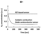
- FIG. 1 outlines the experimental results.
- the vertical axis represents the hydrogen concentration in arbitrary units, and the horizontal axis represents the time axis.
- the graph compares the measurement results of a FET-type hydrogen sensor (FET-based sensor) with a catalytic combustion type and an oxide semiconductor sensor (Oxide semiconductor sensor).
- FET-based sensor FET-based sensor
- Oxide semiconductor sensor oxide semiconductor sensor
- the detailed structure of the FET type hydrogen sensor having a Pt—Ti—O gate structure used in the experiment is detailed in Non-Patent Document 1. It is known that cyclic siloxane is released from asphalt and silicone products used for road paving to the ambient atmosphere, and can cause electrical conduction failure of electrical product contacts at high temperatures.
- the cyclic siloxane Since the catalytic combustion type and the semiconductor type operate at a high temperature of 400 ° C. or higher, the cyclic siloxane is oxidized on the catalyst surface. As a result, it is conceivable that silicon oxide adheres to the surface and covers the active sites of the catalyst for hydrogen, and the catalytic action for hydrogen is lost. In the FET type hydrogen sensor, since the operating temperature is relatively low at about 100 ° C., such a phenomenon does not occur and the activity is considered to be maintained. Since the resistance to cyclic siloxane is high, the FET type hydrogen sensor can be said to be a hydrogen sensor applicable to FCV. The present invention relates to this FET type hydrogen sensor.
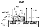
- FIG. 2 explains the hydrogen detection mechanism of the FET type hydrogen sensor which is the subject of the present invention.
- FIG. 2A shows a schematic of a device cross section of a reference FET
- FIG. 2B shows a sensor FET.
- the device cross-sectional structures of the reference FET and the sensor FET are substantially the same including the size and the film configuration. Both are formed on the same silicon substrate (SUB).
- each substrate (SUB) is actually connected, and the reference FET and the sensor FET are formed adjacent to each other on the same substrate (SUB).
- a well (WELL) is provided on a substrate (SUB), and an FET device is formed therein.
- catalyst gate electrodes such as Pt—Ti—O laminated films and Pd films
- the FET type hydrogen sensor in this application covers all the catalyst gates active against hydrogen gas.
- the gate insulating film (OXIDE) is almost composed of SiO2 as in a normal FET.
- the FET type hydrogen sensor of the present application is not limited to this.
- the catalyst gate electrode (CATGATE) is covered with a detection target blocking film (PASSI). Since the detection target blocking film (PASSI) has no hydrogen permeability, hydrogen does not reach the catalyst gate electrode (CATGATE), and thus the reference FET has the same structure as the sensor FET but does not have hydrogen sensitivity.
- the sensor FET has a configuration in which the catalyst gate electrode (CATGATE) is exposed to hydrogen by providing a through hole or the like in a protective film or the like covering the catalyst gate electrode (CATGATE).
- the bias conditions for the sensor FET and reference FET will be described.
- the same drain-source voltage (VDS) is applied to the drain and source terminals of the sensor FET and the reference FET.
- the drain terminal of the reference FET is (DREF)
- the source terminal is (SREF)
- the drain terminal of the sensor FET is (DSEN)
- the source terminal is (SSEN).
- the same gate voltage (VG) is applied to both gates.
- the gate voltage (VG) is a gate potential with respect to the ground potential, and is not a gate potential with respect to the source potential.
- the well potential (BREF) of the reference FET and the source terminal (SREF) are connected, and the well potential (BSEN) of the sensor FET and the source terminal (SSEN) are connected to operate.
- VREF is the output of the reference FET
- (VSEN) is the output of the sensor FET.
- the hydrogen gas is decomposed into hydrogen atoms or hydrogen ions by the catalytic action of the catalyst gate electrode (CATGATE) of the reference FET.
- the decomposed hydrogen is occluded in the catalyst gate electrode (CATGATE) and forms a dipole (DIPOLE) in the vicinity of the interface with the gate insulating film (OXIDE). Due to the action of this dipole (DIPOLE), a threshold voltage change of ⁇ V occurs in the sensor FET as compared with the reference FET, and this is detected by the detection circuit, thereby identifying the hydrogen concentration.
- the device of FIG. 2 has an advantage of detecting a voltage difference because the value of ⁇ V can be increased and the correlation with the hydrogen concentration is strong.
- FIG. 3 shows an outline of a cross-sectional structure of a conventional FET type gas sensor, and the problems are described.
- Two independent P-wells PWELL
- PSUB P-type substrate
- N-channel FET device is formed in each of them.
- One is a sensor FET (NCHSENSOR), and the other is a reference FET (NCHREFERENCE).
- the catalyst metal CATGATE
- PASSI detection target blocking film
- OFIDE gate insulating film
- the P diffusion region (P +) and the N diffusion region (N +) are diffusion layer regions in which impurities are implanted at a high concentration in order to make contact.
- each terminal of the sensor FET is shown as a well potential (BSEN), a drain terminal (DSEN), a gate terminal (GSEN), and a source terminal (SSEN).
- Each terminal of the reference FET is shown as a well potential (BREF), a drain terminal (DREF), a gate terminal (GREF), and a source terminal (SREF).
- the power supply potential of the substrate is indicated by (SUB).
- FIG. 4 is an example of a sensing system including a circuit that detects an output signal of the sensor device shown in FIG. A portion where the well potential is short-circuited through the substrate is indicated by a thick line. As shown in the figure, the substrate potential of the sensor FET and the reference FET is common.
- VTHSENSE Two independent VTH sensing circuits are analog circuit blocks that amplify and extract the outputs of the reference FET and sensor FET, respectively.
- VTHSENSE supplies a drain potential (VDSEN) to the drain terminal (DSEN) of the sensor FET, amplifies the potential (VSSEN) of the source terminal (SSEN), and performs a correction operation on the arithmetic circuit (CAL). Output as sensor output (VSEN).
- the VTH sensing circuit (VTHSENSE) connected to the reference FET supplies the drain potential (VDREF) to the drain terminal (DREF) of the reference FET and the source terminal ( It has a function of amplifying the potential (VSREF) of SREF and outputting it as a sensor output (VREF) to an arithmetic circuit (CAL) that performs a correction operation.
- VDREF drain potential
- DREF drain terminal
- CAL arithmetic circuit
- VTHSENSE The reference FET output and the reference FET output detected by the two VTH sensing circuits (VTHSENSE) are input to the arithmetic circuit (CAL), and the difference between the two sensor outputs (VSEN) and (VREF) is taken to determine the system (SYSTEM). ) As density information (SIG) to be detected.
- the reference voltage generation circuit (VGEN) generates a drain source voltage (VDSSEN) for the sensor FET, a drain source voltage (VDSREF) for the reference FET, and a gate voltage (VG) common to the reference FET and the sensor FET.
- the threshold voltage Vth_sens of the reference FET and the threshold voltage Vth_ref of the sensor FET are described by the following equation (1).
- Vth0 is a threshold voltage including a noise component included in both the reference FET and the sensor FET such as process variations.
- Cox is a gate capacitance
- ⁇ is a dielectric constant
- q is an elementary charge
- NA is a doping concentration
- ⁇ F is Fermi energy
- VG is a gate potential, which are common to the reference FET and the sensor FET.
- Vth_sen (1 / f) is a 1 / f noise component superimposed on the sensor FET output
- Vth_ref (1 / f) is a 1 / f noise component superimposed on the reference FET output.
- ⁇ V is a change in the threshold voltage of the sensor FET due to detection of the target gas, and the reference FET is not in contact with the catalyst gate electrode (CATGATE) of the reference FET due to the detection target blocking film (PASSI) of FIG. This term is not included.
- the second term on the right-hand side is the substrate effect, and is a term that appears due to the difference between the well and source potentials of the reference FET and sensor FET.
- the third term on the right-hand side is a 1 / f noise term well known as FET noise and cannot be removed because it is random noise.
- a reference device and a sensor device are constituted by FETs on a substrate, and the well potentials of both are electrically separated.
- Another aspect of the present invention is a P-type semiconductor substrate, a sensor FET having sensitivity to a detection target formed of a P-type FET in a first N well formed in the P-type semiconductor substrate, and And a reference FET having no sensitivity to a detection target formed by a P-type FET in a second N well formed in the P-type semiconductor substrate.
- the first N well and the second N well are electrically separated, and have a detection circuit that detects a difference in threshold voltage between the sensor FET and the reference FET in a gas atmosphere.
- Another aspect of the present invention relates to a semiconductor substrate, a sensor FET sensitive to a detection target formed of an FET in a first well formed in the semiconductor substrate, and a second formed in the semiconductor substrate.
- This is a system having a reference FET that is not sensitive to a detection target formed of an FET in the well.
- the first well and the second well are electrically separated, the source of the sensor FET and the first well are short-circuited, and the source of the reference FET and the second well are The detection circuit is short-circuited and detects a difference between threshold voltages of the sensor FET and the reference FET in the gas atmosphere.
- Still another aspect of the present invention provides a semiconductor FET on the same semiconductor substrate, and a sensor FET that is formed of a FET in a first well formed in the semiconductor region and is sensitive to an object to be detected.
- a sensor signal output terminal that outputs a threshold voltage of the sensor FET or a signal indicating a change in the threshold voltage
- a reference signal output terminal that outputs a signal indicating the threshold voltage of the reference FET or a change in the threshold voltage are provided.
- Output terminals include both those that output signals outside this device and those that output signals to other circuits within this device.
- the semiconductor region is a first conductivity type semiconductor region
- the first and second wells are second conductivity type wells
- the first and second second conductivity types are used.
- the electrical conduction between the first and second second conductivity type wells is prevented by separating the wells by the first conductivity type semiconductor region.
- the semiconductor substrate may be provided with a structure that generates a signal corresponding to the temperature, and may be used for various controls and corrections to perform accurate measurement.
- the source potential of the sensor FET short-circuited to the well potential may be output to the sensor signal output terminal, and the source potential of the reference FET short-circuited to the well potential may be output to the reference signal output terminal.
- Sectional view of the first embodiment equipped with a thermometer using metal wiring resistance Sectional view of the first embodiment equipped with a thermometer using diffusion layer resistance
- Block diagram of an example of a hydrogen sensor system using the sensor chip of FIGS. 15 and 16 Sectional view of the third embodiment of the P-channel FET type hydrogen sensor chip Sectional drawing of 4th Example of P channel FET type
- mold hydrogen sensor chip Sectional view of the first embodiment of the N channel FET type hydrogen sensor chip Sectional view of the second embodiment of the N-channel FET type hydrogen sensor chip Sectional view of the third embodiment of the N-channel FET type hydrogen sensor chip
- notations such as “first”, “second”, and “third” are attached to identify the constituent elements, and do not necessarily limit the number or order.
- a number for identifying a component is used for each context, and a number used in one context does not necessarily indicate the same configuration in another context. Further, it does not preclude that a component identified by a certain number also functions as a component identified by another number.
- a sensor FET formed of a P-channel FET and a reference FET (PCHREFERENCE) also formed of a P-channel FET are formed adjacent to each other on a P-type substrate (PSUB).
- PSUB P-type substrate
- Both the reference FET and the sensor FET have a catalyst gate (CATGATE), and only the reference FET has a blocking film (PASSI) to eliminate hydrogen sensitivity, which is the same as the conventional configuration shown in FIG.
- the blocking film (PASSI) may be any film that does not transmit the detection target, such as a stable oxide such as silicon nitride or silicon oxide, or various organic films. That is, the first embodiment of the present application is different from the conventional configuration in that the sensor FET and the reference FET are configured not by the N-channel FET but by the P-channel FET while using the same P-type substrate (PSUB).
- N wells (NWELL) in which the respective P channel FETs are formed are provided independently of each other.
- the two NWELLs are reverse-biased when the power supply potential (SUB) of the P-type substrate (PSUB) is set to the ground potential, and thus can be electrically separated.
- the N well (NWELL) potential of the sensor FET and the N well (NWELL) of the reference FET can be controlled independently.
- the well terminal (BSEN) and the source terminal (SSEN) can be short-circuited
- the well terminal (BREF) and the source terminal (SREF) can be short-circuited.
- FIG. 6 shows an example of a sensor system using the sensor chip (SENSORCHIP) shown in FIG.
- the sensor chip (SENSORCHIP) and the detection circuit (DCTCIRCUIT) are separate chips to form a sensor system (SENSORSYSTEM), which is further connected to a host system (SYSTEM).
- the sensor chip and the detection circuit may be combined into one chip, or may be combined into one chip including the host system.
- VTHSEN VTH detection circuit
- VGEN reference voltage generation circuit
- CAL correction operation circuit
- Expression (2) is different in that the term of the substrate effect is eliminated and the 1 / f noise component becomes smaller ( ⁇ ⁇ 1). It is known that 1 / f noise is smaller in a P-channel FET than in an N-channel FET, and ⁇ in the third term on the right side can be expected to be about 0.5. For this reason, in the first embodiment of the present application, the term of the substrate effect is zero and the 1 / f noise component is almost halved as compared with the conventional configuration, so that the detection target can be detected with high accuracy. Further, when FIG. 3 is compared with FIG. 5, the cross-sectional structure hardly changes, so that there is almost no difference in manufacturability. That is, the accuracy of the sensor system can be increased without increasing the manufacturing cost.
- a P-channel FET When using an FET as a normal electronic device, a P-channel FET has a smaller ON current than an N-channel FET, so it is desirable to increase the gate width in order to obtain a sufficient current. That is, there is a concern that the device size must be increased, and the cost increases because the chip area increases.
- a large drain current is not required. Therefore, the disadvantage of the P-channel FET that cannot take a large ON current is not a problem.
- FIG. 7 shows the output characteristics of a sensor FET formed by an actual P-channel FET.
- FIG. 7A shows the hydrogen response characteristics of the sensor output VSEN. It can be seen that the vertical axis is the FET output (arbitrary unit), the horizontal axis is the time axis, and the introduction of hydrogen starts at a timing around several tens of seconds and the output rises. Further, the hydrogen introduction is stopped around 180 seconds, and the output is reduced.
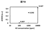
- FIG. 7B shows the relationship between VSEN and hydrogen concentration. Good hydrogen responsiveness has been confirmed at concentrations from 100 ppm to 10,000 ppm, and P-channel sensor FETs have been found to have approximately the same performance as N-channel sensor FETs.
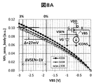
- FIG. 8A shows the relationship between the substrate voltage VBS and the component Vth_sens_body due to the substrate effect of the threshold voltage change in the sensor FET. Calculation was performed for the case where an N-channel FET was used and the well potential was grounded without short-circuiting the well and the source.
- a simplified circuit diagram is as shown in the inset of FIG. 8A.
- G is a gate
- D is a drain
- S is a source.
- a constant current source (ICONS) is inserted between the source and the ground potential to realize a constant drain current as shown in FIG. 2C.
- VDD is a power supply potential
- VG is a gate potential.
- VSEN is a sensor output.
- the temperatures were calculated for 230K, 300K, and 400K, respectively. This corresponds to about ⁇ 40 ° C., room temperature, and 130 ° C., respectively, and covers the operating temperature range required for automotive applications.
- the sensor output (VSEN) and Vth_sens_body increase as the constant current source (ICONS) increases.
- the constant current source (ICONS) is set to a size necessary for sensing
- VBS is about -1.85V
- the sensor output (VSEN) is about 1.85V. This state is assumed when the detection target is 0%.
- the sensor output is 1.0V, which means that VBS is ⁇ 2.85V.
- VBS remains at ⁇ 1.85V. Therefore, a difference of 1.0 V is generated in VBS between the sensor FET and the reference FET.
- the difference ⁇ generated between the threshold voltage of the sensor FET and the threshold voltage of the reference FET becomes 27 mV. Since an error of 27 mV occurs with respect to 3% of detection targets, a measurement error of 2.7% occurs.
- FIG. 8B is a plot of concentration detection relative error of the detection target due to the substrate effect shown in FIG. 8A versus temperature. In addition, it normalized by the relative error in room temperature. This means that when a detection target exists at a concentration of 3%, a relative error of ⁇ 3% is superimposed by the substrate effect when detecting a detection target of 3% at ⁇ 40 ° C. On the other hand, when detecting 3% detection target at 130 ° C., a relative error of + 4% is superimposed by the substrate effect. It should be noted that, as described above, an error superimposed due to the substrate effect has a temperature dependency, and in order to correct this, temperature calibration is required as a pre-shipment adjustment of the sensor. This can cause an increase in sensor cost.
- the Vth variation Vth_body due to the substrate effect is described as in the following formula (3).
- T is the temperature
- Ni is the intrinsic carrier density. Since the impurity density NA has temperature dependence, Vth_body changes depending on the temperature.
- FIG. 9 shows a 1 / f noise calculated using a standard N-channel FET model TypN and a standard P-channel FET model TypP provided in a certain semiconductor manufacturing process FAB-A, and compared between the P-channel FET and the N-channel FET. It is.
- the following formula (4) which is a 1 / f noise calculation formula in BSIM3, was used for the calculation.
- vn is the gate input equivalent noise
- ⁇ f is the bandwidth
- KF is the 1 / f noise parameter
- L is the gate length of the FET
- W is the gate width of the FET
- f is the measurement frequency.
- the noise level in FAB-A is about two orders of magnitude lower for both the N channel and the P channel than the output when the detection target is 10 ppm.
- the magnitude of 1 / f noise is about the same as the signal output of the detection target 10 ppm, and cannot be ignored.
- the P-channel type is advantageous for higher accuracy than the N-channel type.
- 1 / f noise is random noise and cannot be removed by the difference between the reference FET and the sensor FET. Therefore, it is desirable to make it as small as possible at the sensor chip level. Further, since the 1 / f noise becomes larger as the measurement time becomes longer, it is possible to improve stability and reliability with respect to long-time operation by configuring the sensor FET and the reference FET with P-channel FETs.
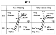
- the behavior when detecting the detection target gas (Gas ⁇ detecting) and the behavior when the ambient temperature rises (Temperature rising) are compared between the P-channel FET (PCH) and the N-channel FET (NCH).
- PCH P-channel FET
- NCH N-channel FET
- the behavior of the sensor FET when a detection target gas is detected will be described.
- the dotted line indicates the IDS-VGS characteristics when no gas is present
- the solid line indicates the gas when the gas is present.
- the threshold voltage VTH decreases in the detection target gas atmosphere, and conversely increases in the P-channel sensor FET.
- the decrease in VTH in the P-channel sensor FET means that the gate-source voltage VGS necessary for obtaining the same drain current IDS decreases.
- VTH decreases in the N-channel FET and VTH also decreases in the P-channel FET compared to before the temperature rise.
- the dotted line is the IDS-VGS characteristic before the temperature rise and the solid line is the temperature after the temperature rise.
- the direction of change of VTH is the same when the detection target gas is detected and when the temperature rises, whereas the P-channel sensor FET is opposite.
- the output direction of the P-channel sensor FET is reversed, so that the VTH change due to detection of the detection target gas and the VTH change due to temperature rise can be clearly separated.
- the N-channel sensor FET cannot be separated.
- the P-channel sensor FET is more advantageous than the N-channel in the sense that the possibility of erroneous detection can be reduced.
- the N-channel sensor FET is more suitable than the P-channel when the generation of the detection target gas is accompanied by a temperature drop.
- the above is a P-channel FET, which is an effect obtained by configuring a sensor FET and a reference FET.
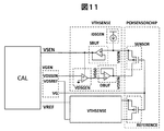
- FIG. 11 describes an example of a specific configuration of the VTH detection circuit (VTHSENSE) in the sensor system (SENSORSYSTEM) shown in FIG.
- the output of the drain source current generation circuit (IDSGEN) that generates a constant drain current is connected to the source potential (VSSEN) for the sensor FET (SENSOR).
- the source voltage buffer (SBUF) receives the source potential (VSSEN) as an input and outputs the same voltage as the input to the sensor FET device output (VSEN). Thereby, even if the load of the sensor FET device output (VSEN) is large, the voltage level of the source potential (VSSEN) can be transmitted to the arithmetic circuit (CAL).
- CAL arithmetic circuit
- the drain source voltage generation circuit receives the drain source voltage (VDSSEN) for sensor FET and the sensor FET device output (VSEN) generated by the voltage generation circuit (VGEN) and outputs (VDS0).
- the drain / source voltage generation circuit VDSGEN
- VDSGEN drain / source voltage generation circuit
- VTH detection circuit VTHSENSE
- PCHSENSORCHIP P-type FET sensor chip
- DBUF drain voltage buffer
- the VTH detection circuit (VTHSENSE) on the reference FET (REFERENCE) side is basically the same as that on the sensor FET side.
- the operational amplifier in FIG. 11 may be a commercially available operational amplifier having general characteristics.
- FIG. 12 shows a second embodiment of the sensor chip.
- the P-channel sensor FET and the P-channel reference FET are formed on the P-type substrate (PSUB) as in the first embodiment shown in FIG. 5 except that the gate of the reference FET catalyzes the detection target. It is different in that it is composed of a gate (GATE) that does not have a gate. In this configuration, it is possible to essentially avoid the defect that the reference FET has sensitivity to the detection target due to the deterioration of the blocking film (PASSI) shown in FIG. However, it is necessary to separately form a gate (GATE) having no catalytic action and a catalyst gate electrode (CATGATE) separately, which increases the film forming process cost and the number of masks.
- GATE gate having no catalytic action
- CAGATE catalyst gate electrode
- FIG. 13 shows a second embodiment of the sensor system.
- the number of VTH sensing circuits (VTHSENSE) is reduced to one, and the sensor FET and the reference FET share one VTH sensing circuit (VTHSENSE) via the switch SW. .
- the switch control signal (SWCTRL) is generated by the correction arithmetic circuit (CAL).
- FIG. 14 shows a third embodiment of the sensor chip. It is the structure which added the PN junction thermometer (TEMPMETER) to the 1st Example shown in FIG.
- the PN junction is formed on the same P-type substrate (PSUB) as the P-channel sensor FET and the P-channel reference FET.
- the anode terminal (APN) is connected to the P diffusion region (P +), and the cathode terminal (CPN) is connected to the N diffusion region (N +).
- the wells (NWELL) of the sensor FET, reference FET, and PN junction are electrically isolated from each other by setting the substrate potential (SUB) to the ground potential.
- the gate of the reference FET in FIG. 14 is a catalyst gate electrode (CATGATE), but may be a gate without a catalytic action (GATE) as shown in FIG.
- CAGATE catalyst gate electrode
- GATE catalytic action
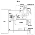
- FIG. 15 shows an embodiment of a third sensor system including the sensor chip of FIG. Compared with FIG. 6, the sensor chip includes a thermometer (TEMPMETER) configured by a PN junction, and a circuit block for controlling the thermometer (TEMPMETER) is added.
- a thermometer configured by a PN junction
- a circuit block for controlling the thermometer is added.
- the current source (IDIODEGEN) generates a current to be supplied to the thermometer (TEMPMETER).
- VGEN reference voltage generation circuit
- VDIODE voltage for appropriately controlling the thermometer
- the temperature of the sensor chip is obtained by the arithmetic circuit (CAL) using the anode potential (VF) of the thermometer (TEMPMETER).
- the arithmetic circuit (CAL) uses the obtained chip temperature information to carry out control for keeping the chip temperature constant and calculation for correcting the sensitivity of the sensor output. Since the FET type gas sensor obtains an output by occlusion of the detection target gas in the catalyst metal, the sensitivity changes depending on the chip temperature. Therefore, it is desirable to provide a thermometer on the chip to perform sensitivity correction in order to ensure reliability in an application where the environmental temperature changes.
- FIG. 16 shows a fourth embodiment of the sensor chip.
- a thermometer (TEMPMETER) is constituted by wiring resistance.
- FIG. 16 shows a section of the entire wiring resistance, and it is assumed that a wiring having a necessary length is actually formed on the chip.
- One end of the wiring is taken out as an RH terminal (RH), and the other end is taken out as an RL terminal (RL). Since the metal wiring resistance is a function of temperature, chip temperature information can be obtained by measuring the resistance value.
- the above wiring thermometer can also be used as an electric heater for adjusting the chip temperature.
- the RH terminal (RH) and the RL terminal (RL) serve both as a heater power supply connection terminal and a resistance measurement terminal.
- the RH terminal is separately prepared as RH1 and RH2, and the RL terminal (RL) is prepared as RL1 and RL2.
- the gate of the reference FET may be replaced with a non-catalytic gate (GATE), and the detection target blocking film (PASSI) may be omitted. That is, the case where the wiring resistance thermometer is applied to the second embodiment of the sensor chip shown in FIG. 12 is also included in the scope of the present application.
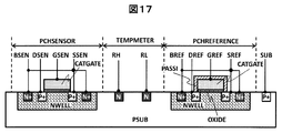
- FIG. 17 shows a fifth embodiment of the sensor chip.
- a resistance thermometer (TEMPMETER) is formed of a diffusion layer resistance.
- a wiring resistance thermometer there is an advantage of high stability.
- the heat generation efficiency can be improved when it is used as an electric heater.
- the wiring is embedded in the P-type substrate (PSUB), the thermal efficiency when used as a heater can be improved as compared with the wiring resistance thermometer.
- the RH terminal (RH) and the RL terminal (RL) serve both as a heater power supply connection terminal and a resistance measurement terminal.
- the diffusion layer resistance thermometer In order to accurately measure the resistance value, four-terminal measurement is desirable. Therefore, there is a method in which the RH terminal (RH) is separately prepared as RH1 and RH2, and the RL terminal (RL) is prepared as RL1 and RL2. Since the diffusion layer resistance thermometer can be manufactured at the same time in the diffusion layer manufacturing process, it is preferable that an increase in process cost can be suppressed. As described with reference to FIG. 14, the gate of the reference FET may be replaced with a non-catalytic gate (GATE), and the detection target blocking film (PASSI) may be omitted. That is, the case where the diffusion layer resistance thermometer is applied to the second embodiment of the sensor chip shown in FIG. 12 is also included in the scope of the present application.
- GATE non-catalytic gate
- PASSI detection target blocking film
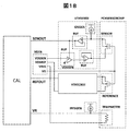
- FIG. 18 shows an embodiment of a fourth sensor system of the sensor system using the sensor chip shown in FIGS.
- the thermometer (TEMPMETER) is different from that of the resistor.
- the current source (IRESGEN) is a circuit block that generates a current for controlling a thermometer (TEMPMETER).
- the reference voltage generation circuit (VGEN) generates a resistance thermometer control voltage (VRES).
- the resistance thermometer output (VR) is input to the arithmetic circuit (CAL).
- CAL arithmetic circuit
- FIG. 19 shows a sixth embodiment of the sensor chip.
- a deep P well (DPWELL) is provided on the N-type substrate (NSUB), and a P-channel sensor FET and a P-channel reference FET are further formed thereon.
- the process cost for forming the deep P well increases, it is effective for applications where an N-type substrate (NSUB) must be used.
- the substrate potential (SUB) needs to be a high potential that is not grounded.
- FIG. 20 shows a seventh embodiment of a sensor chip in which a P-channel sensor FET and a P-channel reference FET are configured without a deep well on an N-type substrate (NSUB).
- a trench type element isolation STI
- the impedance between the well of the sensor FET and the well of the reference FET increases, so that the well potential can be controlled independently.
- a configuration in which the substrate effect is eliminated by short-circuiting the source and well can be realized.
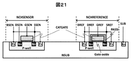
- FIG. 21 shows an eighth embodiment in which the P-type substrate is replaced with an N-type substrate (NSUB) and the P-channel FET is replaced with an N-channel FET in the first embodiment shown in FIG.
- N-type substrate N-type substrate
- FIG. 22 shows that the N-type substrate is replaced with a P-type substrate (PSUB), the deep P-well is replaced with a deep N-well (DNWELL), and the P-channel FET is replaced with an N-channel FET with respect to the sixth embodiment shown in FIG. This is the ninth embodiment.
- FIG. 23 shows a tenth embodiment in which the N-type substrate is replaced with a P-type substrate (PSUB) and the P-channel FET is replaced with an N-channel FET in the seventh embodiment shown in FIG.
- PSUB P-type substrate
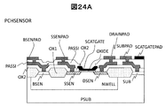
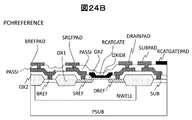
- FIG. 24 is an example of a cross-sectional structure diagram in the case where the semiconductor element is configured by the P-channel FET shown in FIG.
- An N well (NWELL) is formed on a P type substrate (PSUB), and a P type FET is formed therein.
- Both the sensor FET (PCHENSENSOR) and the reference FET (PCHREFERENCE) have a catalyst gate electrode (SCATGATE, RCATGATE), but the sensor FET catalyst gate electrode (SCATGATE) is a through-hole formed in the blocking film (PASSI). Whereas the exposed gate electrode (RCATGATE) of the reference FET is covered with a blocking film (PASSI).
- a gate oxide film (OXIDE) is present under the catalyst gate electrode. Further, there are an element isolation film (OX1) and an interlayer film (OX2).
- the drain terminal (DREF) of the reference FET is the drain pad (DRAINPAD)
- the source terminal (SREF) of the reference FET is the source pad (SREFPAD)
- the well terminal (BREF) of the reference FET is the body pad (BREFPAD)
- the catalyst gate The electrode (RCATGATE) is connected to the gate pad (RCATGATEPAD)
- the substrate (SUB) is connected to the substrate potential pad (SUBPAD), so that signals can be input and output.
- the drain terminal (DSEN) of the sense FET is connected to the drain pad (DRAINPAD)
- the source terminal (SSEN) of the reference FET is connected to the source pad (SSENPAD)
- the well terminal (BSEN) of the reference FET is connected to the body pad (BSENPAD)
- the catalyst gate is connected to the electrodes (SCATGATE)
- SCATGATE are connected to gate pads (SCATGATEPAD), respectively, and can input and output signals.
- the present invention is not limited to the above-described embodiment, and includes various modifications. For example, a part of the configuration of one embodiment can be replaced with the configuration of another embodiment, and the configuration of another embodiment can be added to the configuration of one embodiment. Further, it is possible to add, delete, and replace the configurations of other embodiments with respect to a part of the configurations of the embodiments.
- the functions of the “source” and “drain” of the transistor may be switched when a transistor with a different polarity is used or when the direction of current changes during circuit operation. Therefore, in this specification, the terms “source” and “drain” may be used interchangeably depending on circumstances.
- Electrode and “wiring” do not functionally limit these components.
- an “electrode” may be used as part of a “wiring” and vice versa.
- the terms “electrode” and “wiring” include a case where a plurality of “electrodes” and “wirings” are integrally formed.
- the FET type sensor of the present invention is a technology applicable to hydrogen concentration meters in various plants and nuclear power plants, including hydrogen infrastructure such as fuel cell vehicles and hydrogen stations.
Landscapes
- Chemical & Material Sciences (AREA)
- Health & Medical Sciences (AREA)
- Life Sciences & Earth Sciences (AREA)
- Physics & Mathematics (AREA)
- General Physics & Mathematics (AREA)
- Engineering & Computer Science (AREA)
- Biochemistry (AREA)
- Pathology (AREA)
- Immunology (AREA)
- General Health & Medical Sciences (AREA)
- Analytical Chemistry (AREA)
- Microelectronics & Electronic Packaging (AREA)
- Electrochemistry (AREA)
- Chemical Kinetics & Catalysis (AREA)
- Molecular Biology (AREA)
- Crystallography & Structural Chemistry (AREA)
- Computer Hardware Design (AREA)
- Nonlinear Science (AREA)
- Combustion & Propulsion (AREA)
- Food Science & Technology (AREA)
- Medicinal Chemistry (AREA)
- Investigating Or Analyzing Materials By The Use Of Electric Means (AREA)
- Element Separation (AREA)
- Semiconductor Integrated Circuits (AREA)
- Metal-Oxide And Bipolar Metal-Oxide Semiconductor Integrated Circuits (AREA)
- Insulated Gate Type Field-Effect Transistor (AREA)
Abstract
FET型水素センサのセンス信号を低ノイズ化する。 上記課題を解決するために、本発明のセンサシステムの一側面は基板上にFETにより参照デバイスとセンサデバイスを構成し、更に両者のウェル電位は電気的に分離する。
Description
本発明は、FET型センサシステムにおいて、センサデバイスと参照デバイスの出力の差分から対象物を検知する際に、高精度に対象物を検知する技術に関する。
地球環境保全の観点から温室効果ガスであるCO2の排出量削減が地球規模の課題である。自動車からの排出を抑制するため、燃焼しても水しか排出しない、水素を燃料とする燃料電池自動車(FCV)の開発が進んでいる。FCVでは水素燃焼時の水素濃度制御、配管からの水素漏えい検知のための水素濃度計の搭載が望ましい。特に水素は空気中の濃度が3.9%に達すると爆発することが知られているため、水素の漏えい検知用途では上記爆発限界濃度に達する前に水素濃度計によりアラートを発するといった安全対策が望ましい。また燃焼時の水素濃度を最適化することで燃費性能を向上可能であるため、燃焼条件にフィードバックをかける目的で水素濃度の監視が望ましい。
現在実用化されている水素センサは、接触燃焼式、半導体式、気体熱伝導式などがある。上記以外にも開発段階の方式として固体電解質型とFET型がある。
接触燃焼式はプラチナ(Pt)やパラジウム(Pd)といった触媒金属表面で水素が燃焼し、これによる触媒金属の温度上昇を検出する方式である。水素感度が高いが選択性が低い、検出に酸素が必要、出力が小さいため検出回路に工夫を要する、動作温度が400℃程度と高くデバイスを高温に保持する必要があるため消費電力が大きい、といった欠点がある。
半導体式は金属酸化物半導体表面における水素の酸化反応により半導体内の空乏層が変化するためキャリア濃度が変化し、これに伴う電気伝導の変化を検出する。金属酸化物半導体表面における酸化反応を起こすために酸素を必要、動作温度が500℃程度と高くデバイスを高温に保持する必要があるため消費電力が大きい、といった欠点がある。
気体熱伝導式は、雰囲気ガス中に水素が混入することで熱伝導率が変化するため、素子から放出される熱量の変化量を検出することで水素を検出する。動作温度が200℃程度と比較的低いため消費電力が小さいことは利点だが、低濃度水素の検出が難しいため水素漏えい検知用途には向かない。
また、FET(電界効果トランジスタ)型センサについては、Pt-Ti-Oゲート構造を持つ例が非特許文献1に開示されている。
IEEE Sensors Journal, vol. 12,No.6,June 2012. "Pt-Ti-O Gate Si-MISFET Hydrogen Gas Sensors-Devices and Packagings "
実用化されている水素センサをFCVにおける水素漏えい検知に使う場合、低濃度の水素を精度よく検出可能な接触燃焼式と半導体式が候補となる。しかしこれらの方式には環境物質である環状シロキサン被毒に弱いという欠点があることを我々は実験により見出した。これに対してPt-Ti-Oゲート構造を有するFET型水素センサは環状シロキサン被毒耐性が高いことも、発明者らは同時に実験により確認している。
図1に実験結果の概略を示す。縦軸に水素濃度を任意単位で、横軸に時間軸を示す。グラフはFET型水素センサ(FET-based sensor)と、接触燃焼式(Catalytic combustion)および酸化物半導体センサ(Oxide semiconductor sensor)の測定結果を対比したものである。なお、実験に用いたPt-Ti-Oゲート構造を持つFET型水素センサの詳細な構造については非特許文献1に詳しい。環状シロキサンは道路の舗装に用いるアスファルトやシリコーン製品から環境雰囲気に放出され、高温では電気製品の接点の導通不良の原因になりうることが知られている。
図1によると、例えば0.5程度の水素濃度中で測定を行っている場合、接触燃焼式と半導体式は環状シロキサン雰囲気中では100秒程度で水素に対する活性を急激に失い、感度が低下するため、検出される水素濃度が低下する。一方でFET型水素センサでは触媒活性がほとんど変化しないため、検出される水素濃度は変化しない。
接触燃焼式と半導体式は400℃以上の高温で動作するため、触媒表面で環状シロキサンが酸化される。この結果、シリコン酸化物が表面に付着して水素に対する触媒の活性サイトを覆ってしまい、水素に対する触媒作用が失われるメカニズムが考えられる。FET型水素センサでは動作温度が100℃程度と比較的低いためこのような現象が起こらず、活性が維持されると考えられる。環状シロキサン耐性が高いことからFET型水素センサはFCVに適用することが可能な水素センサということができる。本願発明はこのFET型水素センサに関するものである。
図2により、本願発明で対象とするFET型水素センサの水素検知メカニズムを説明する。
図2Aは参照FET、図2BはセンサFETのデバイス断面の概略を示している。参照FETとセンサFETのデバイス断面構造はサイズや膜構成を含めてほぼ同一に作製される。両者は同一のシリコン基板(SUB)上に形成される。つまり図2では図2A、図2Bと分離して記載しているが、実際はそれぞれの基板(SUB)はつながっており、同じ基板(SUB)上に参照FETとセンサFETが隣接して形成される。基板(SUB)上にウェル(WELL)を設け、この中にFETデバイスを形成する。
触媒ゲート電極(CATGATE)はPt-Ti-Oの積層膜やPd膜など様々な種類が存在するが本願中におけるFET型水素センサでは水素ガスに対して活性を持つ触媒ゲート全てを対象とする。ゲート絶縁膜(OXIDE)は通常のFETと同様にSiO2で構成されることがほとんどである。しかし本願のFET型水素センサはこれに限定するものではない。参照FETは触媒ゲート電極(CATGATE)が検出対象遮断膜(PASSI)で覆われる。検出対象遮断膜(PASSI)は水素透過性が無いため水素が触媒ゲート電極(CATGATE)まで到達せず、よって参照FETはセンサFETと同一の構造を持ちながらも水素感応性を持たない。
センサFETでは、図2では図示していないが、触媒ゲート電極(CATGATE)を覆う保護膜等にスルーホール等を設けることにより、触媒ゲート電極(CATGATE)が水素にさらされる構成となっている。
センサFETと参照FETのバイアス条件について説明する。センサFETと参照FETには同じドレインソース電圧(VDS)がそれぞれのドレイン、ソース端子に印加される。参照FETのドレイン端子は(DREF),ソース端子は(SREF),センサFETのドレイン端子は(DSEN),ソース端子は(SSEN)と示した。さらに両者のゲートには同一のゲート電圧(VG)を印加する。ゲート電圧(VG)は接地電位を基準とするゲート電位であり、ソース電位に対するゲート電位ではない。参照FETのウェル電位(BREF)とソース端子(SREF)を接続し、センサFETのウェル電位(BSEN)とソース端子(SSEN)を接続して動作させる。これによりFETの閾電圧が基板の電圧により変動する基板効果を除去することが出来る。(VREF)は参照FETの出力であり、(VSEN)はセンサFETの出力である。
図2Bに示す通り、参照FETの触媒ゲート電極(CATGATE)の触媒作用により、水素ガスは水素原子もしくは水素イオンに分解される。この分解された水素は触媒ゲート電極(CATGATE)に吸蔵され、ゲート絶縁膜(OXIDE)との界面付近に双極子(DIPOLE)を形成する。この双極子(DIPOLE)の作用によりセンサFETには参照FETと比較してΔVの閾電圧変化が生じ、これを検出回路により検出することで水素濃度を同定する。
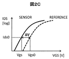
図2Cは水素検知時の参照FETとセンサFETのIDS-VDS特性を比較した概略図である。同一のドレインからソースに流れる電流(IDS)が印加されているため動作電流は同一である。また同一のドレインソース電圧(VDS)が印加されているためIDS-VGS曲線は参照FET(点線で示す)とセンサFET(実線で示す)で同じ形となり、ΔVだけセンサFETの曲線がVGSの負側にシフトした形となる。このように閾電圧変化ΔVが参照FETにおけるゲートソース電圧Vgs0とセンサFETにおけるゲートソース電圧Vgsの差分として現れる。前述の通りVGは参照FETとセンサFETで同一なので、Vgs=VG-VSよりΔVは両者のソース電位の差分として最終的に検出される。
なお、動作方法としては、上記のように電流を一定として電圧の差ΔVを検出する動作方法のほか、電圧を一定として電流の差ΔIを検出する動作方法もある。図2のデバイスでは、ΔVの値が大きくとれ、また、水素濃度との相関が強いため、電圧差を検出するメリットがある。
これまでの説明では検知対象ガスとして水素の例を説明してきたが、FET型センサでは触媒金属CATGATEの種類を変更することにより水素以外の様々なガス検知が可能になることから、以下の説明ではFET型ガスセンサ全般の課題について述べる。
図3に従来のFET型ガスセンサの断面構造の概略を示し、課題を説明する。P型基板(PSUB)上に2つの独立したPウェル(PWELL)を設け、その中にそれぞれ1つずつのNチャネルFETデバイスを形成する。一つはセンサFET(NCHSENSOR)であり、もう一つは参照FET(NCHREFERENCE)である。触媒金属(CATGATE),検知対象遮断膜(PASSI),ゲート絶縁膜(OXIDE)は図2と同じである。P拡散領域(P+)、N拡散領域(N+)はそれぞれコンタクトを取るために高濃度に不純物を打ち込んだ拡散層領域である。
図2と同じく、センサFETの各端子を、ウェル電位(BSEN)、ドレイン端子(DSEN)、ゲート端子(GSEN)、ソース端子(SSEN)として示す。参照FETの各端子を、ウェル電位(BREF)、ドレイン端子(DREF)、ゲート端子(GREF)、ソース端子(SREF)として示す。基板の給電電位を(SUB)で示す。これらの記号は、明細書中で共通に用いることにする。
図3から分かる通り、同一のP型基板(PSUB)上にPウェル(PWELL)を隣接して作成するため、参照FETとセンサFETのウェルは低抵抗で電気的に接続される。このため、図2A、図2Bで示したようにウェルとソースを短絡することが出来ない。このような状態で参照FETとセンサFETの出力の差分により水素を検知する際には、以下に説明する通り基板効果を除去することができず、検知対象物の濃度算出が困難になる。
図4は図3に記載のセンサデバイスの出力信号を検出する回路を含めたセンシングシステムの一例である。ウェル電位が基板を介して短絡されている部分を太い線で示した。図示されるように、センサFETと参照FETの基板電位が共通となっている。独立した2つのVTHセンシング回路(VTHSENSE)は、それぞれ参照FETとセンサFETの出力を増幅して取り出すアナログ回路ブロックである。
VTHセンシング回路(VTHSENSE)は、センサFETのドレイン端子(DSEN)にドレイン電位(VDSEN)を供給し、ソース端子(SSEN)の電位(VSSEN)を増幅し、補正演算を行う演算回路(CAL)にセンサ出力(VSEN)として出力する。
参照FETに接続されるVTHセンシング回路(VTHSENSE)も上記センサFETに接続されたVTHセンシング回路(VTHSENSE)と同様、参照FETのドレイン端子(DREF)にドレイン電位(VDREF)を供給し、ソース端子(SREF)の電位(VSREF)を増幅し、補正演算を行う演算回路(CAL)にセンサ出力(VREF)として出力する機能を有する。
上記2つのVTHセンシング回路(VTHSENSE)で検出された参照FET出力と参照FET出力は演算回路(CAL)に入力され、2つのセンサ出力(VSEN)と(VREF)の差分を取って、システム(SYSTEM)に検知対象の濃度情報(SIG)として渡される。
基準電圧生成回路(VGEN)は,センサFET向けドレインソース電圧(VDSSEN)、参照FET向けドレインソース電圧(VDSREF)、参照FETとセンサFETに共通のゲート電圧(VG)を生成する。
図3と図4で構成されるセンサシステムにおいて、参照FETの閾電圧Vth_sensとセンサFETの閾電圧Vth_refは以下の式(1)で記述される。

ここでVth0はプロセスばらつきなどの参照FETとセンサFETに共通して含まれる雑音成分を含んだ閾電圧である。Coxはゲート容量、εは誘電率、qは素電荷、NAはドーピング濃度、φFはフェルミエネルギー、VGはゲート電位であり、それぞれ参照FETとセンサFETに共通である。Vth_sen(1/f)はセンサFET出力に重畳される1/fノイズ成分、Vth_ref(1/f)参照FET出力に重畳される1/fノイズ成分である。ΔVは対象ガスを検知したことによるセンサFETの閾電圧の変化分であり、参照FETは図3の検知対象遮断膜(PASSI)により対象ガスが参照FETの触媒ゲート電極(CATGATE)に接触しないためこの項が含まれない。
上記2つの式の差分からΔVだけが残ることが望ましい。しかし、右辺第2項と第3項は差分により除去することが出来ない。これがガス検出時の誤差として残りセンサシステム全体の計測精度や信頼性を劣化させる。右辺第2項は基板効果であり、参照FET、センサFETそれぞれの、ウェルとソースの電位に差が生じる為に現れる項である。右辺第3項はFETのノイズとして良く知られる1/fノイズの項であり、これはランダム雑音であるため除去ができない。
上記課題を解決するために、本発明のセンサシステムの一側面は基板上にFETにより参照デバイスとセンサデバイスを構成し、更に両者のウェル電位は電気的に分離する。
本発明の他の一側面は、P型半導体基板と、P型半導体基板に形成された第一のNウェル内にP型FETで形成された検知対象物に対して感応性を持つセンサFETと、P型半導体基板に形成された第二のNウェル内にP型FETで形成された検知対象に対して感応性を持たない参照FETと、を有するシステムである。このシステムは、第一のNウェルと第二のNウェルは電気的に分離され、ガス雰囲気中における前記センサFETと前記参照FETの閾電圧の差分を検出する検出回路とを有する。
本発明の他の側面は、半導体基板と、半導体基板に形成された第一のウェル内にFETで形成された検知対象に対して感応性をもつセンサFETと、半導体基板に形成された第二のウェル内にFETで形成された検知対象に感応性を持たない参照FETとを有するシステムである。ここで、第一のウェルと第二のウェルとは電気的に分離して設けられ、センサFETのソースと第一のウェルとが短絡されており、参照FETのソースと第二のウェルとが短絡されており、ガス雰囲気中におけるセンサFETと参照FETの閾電圧の差分を検出する検出回路とを有する。
本発明のさらに他の側面は、同一の半導体基板に、半導体領域と、半導体領域に形成された第一のウェル内にFETで形成された、検知対象物に対して感応性を持つセンサFETと、半導体領域に形成された第二のウェル内にFETで形成された、検知対象に対して感応性を持たない参照FETとを有するデバイスである。このデバイスは、第一のウェルと第二のウェルの間の電気的導通を妨げる構成を備える。また、センサFETの閾値電圧または閾値電圧の変化を示す信号を出力するセンサ信号出力端子と、参照FETの閾電圧または閾値電圧の変化を示す信号を出力する参照信号出力端子とを備える。出力端子は、このデバイスの外に信号を出力するものと、このデバイス内の他の回路に対して信号を出力するものの両者を含む。
電気的導通を妨げる構成として好ましい一例としては、半導体領域を第1導電型の半導体領域とし、第一及び第二のウェルを第2導電型のウェルとし、第一及び第二の第2導電型ウェルの間を第1導電型の半導体領域で分離することにより、前記第一及び第二の第2導電型ウェルの間電気的導通を妨げる例が挙げられる。
また、電気的導通を妨げる他の構成例としては、第一及び第二のウェルの間に、トレンチ型素子分離構造を設けることにより、前記第一及び第二の第2導電型ウェルの間電気的導通を妨げる例が挙げられる。
半導体基板には、温度に対応した信号を発生する構造を設けておき、種々の制御や補正に用いて、正確な測定を行うようにしてもよい。
また、好ましい構成例としては、センサFETのウェル電位とソース電位を短絡し、参照FETのウェル電位とソース電位を短絡することがあげられる。また、ウェル電位と短絡されたセンサFETのソース電位をセンサ信号出力端子に出力し、ウェル電位と短絡された参照FETのソース電位を参照信号出力端子に出力するように構成してもよい。
FET型センサのセンス信号の低ノイズ化を図ることができる。上記した以外の課題、構成、及び効果は、以下の実施形態の説明により明らかにされる。
以下、本発明の実施の形態を図面に基づいて詳細に説明する。ただし、本発明は以下に示す実施の形態の記載内容に限定して解釈されるものではない。本発明の思想ないし趣旨から逸脱しない範囲で、その具体的構成を変更し得ることは当業者であれば容易に理解される。なお、実施の形態を説明するための全図において、同一の部材には原則として同一の符号を付し、その繰り返しの説明は省略することがある。
本明細書等における「第1」、「第2」、「第3」などの表記は、構成要素を識別するために付するものであり、必ずしも、数または順序を限定するものではない。また、構成要素の識別のための番号は文脈毎に用いられ、一つの文脈で用いた番号が、他の文脈で必ずしも同一の構成を示すとは限らない。また、ある番号で識別された構成要素が、他の番号で識別された構成要素の機能を兼ねることを妨げるものではない。
図面等において示す各構成の位置、大きさ、形状、範囲などは、発明の理解を容易にするため、実際の位置、大きさ、形状、範囲などを表していない場合がある。このため、本発明は、必ずしも、図面等に開示された位置、大きさ、形状、範囲などに限定されない。
本明細書において単数形で表される構成要素は、特段文脈で明らかに示されない限り、複数形を含むものとする。
図5に示すセンサチップの断面図は本願の第一の実施例である。P型基板(PSUB)上にPチャネルFETで形成されたセンサFET(PCHSENSOR)と、同じくPチャネルFETで形成された参照FET(PCHREFERENCE)とが、互いに隣接して形成される。互いに隣接して同じ構造の参照FETとセンサFETを形成することで、リソグラフィーやインプラ濃度に代表される製造ばらつきを抑制でき、差分を取るさいの誤差を低減することが可能となる。
参照FET、センサFET共に触媒ゲート(CATGATE)を有し、参照FETのみが水素感応性を無くすために遮断膜(PASSI)を有する点は図3に示した従来構成と同じである。遮断膜(PASSI)は例えば窒化シリコンや酸化シリコンといった安定な酸化物や各種有機膜など、検出対象を透過しない膜であれば何でも良い。すなわち、本願の第一実施例は従来構成と比較して同じP型基板(PSUB)を使用しながら、NチャネルFETでなく、PチャネルFETでセンサFETと参照FETを構成する点が異なる。
それぞれのPチャネルFETが形成されるNウェル(NWELL)は互いに独立して設けられる。この結果、上記2つのNWELLはP型基板(PSUB)の給電電位(SUB)を接地電位としたときに逆バイアスされるため、電気的に分離することが可能となる。
このため、センサFETのNウェル(NWELL)電位と参照FETのNウェル(NWELL)とは独立してその電位を制御することができる。結果として、図5に示す通りセンサFETにおいてはウェル端子(BSEN)とソース端子(SSEN)を短絡し、参照FETにおいてはウェル端子(BREF)とソース端子(SREF)を短絡することが可能となる。
図6には図5に示したセンサチップ(SENSORCHIP)を用いたセンサシステムの一例を示す。この例では、センサチップ(SENSORCHIP)と検出回路(DCTCIRCUIT)を別チップとし、センサシステム(SENSORSYSTEM)を構成し、これをさらに上位システム(SYSTEM)に接続している。しかし、センサチップと検出回路を1チップに纏めてもよいし、さらに上位システムまで含めて1チップに纏めてもよい。
VTH検出回路(VTHSEN),基準電圧生成回路(VGEN),補正演算回路(CAL)の動作は図4の説明と同等である。ただし、図4ではNチャネルFETであったのに対し図6ではPチャネルFETであるためソースとドレインが入れ替わる。図6のセンサチップ(SENSORCHIP)においてPチャネルセンサFET(PCHSENSOR)とPチャネル参照FET(PCHREFERENCE)それぞれにおいてウェル電位とソース電位が短絡されている点が図3に示す従来例と異なる。これにより図6に示すセンサシステムにおいて、参照FETの閾電圧Vth_sensとセンサFETの閾電圧Vth_refは以下の式(2)で記述される。

式(1)と比較すると、式(2)では基板効果の項が無くなり、更に1/f雑音成分がそれぞれ小さくなる(α<1)点が異なる。PチャネルFETでは1/f雑音がNチャネルFETに比較して小さいことが知られており、右辺第3項におけるαは、0.5程度が期待できる。このため、本願第一の実施例では従来構成に比較して基板効果の項がゼロとなり1/f雑音成分がほぼ半減することから、検知対象を精度よく検出することが可能となる。また図3と図5を比較した時、その断面構造はほとんど変化しないことから製造容易性にほとんど違いが生じない。すなわち、製造コストを増加させることなくセンサシステムの高精度化が可能となる。
通常の電子デバイスとしてFETを使う場合、PチャネルFETはNチャネルFETに比較してON電流が小さいため、十分な電流を得る為にはゲート幅を大きくすることが望ましい。すなわち、デバイスサイズを大きくしなければいけなくなり、チップ面積が大きくなるからコストが増加するという懸念がある。しかし、参照FETとセンサFETの閾電圧の差分から対象を検知する図6に示すセンサシステムとして使う場合、大きなドレイン電流を必要としない。よってON電流を大きくとれないPチャネルFETの欠点は問題とならない。
図7には実際のPチャネルFETで形成されたセンサFETの出力特性を示す。図7Aはセンサ出力VSENの水素応答特性である。縦軸がFETの出力(任意単位)、横軸は時間軸で、数十秒付近のタイミングで水素の導入を開始するとともに、出力が立ち上がっているのが分かる。また、180秒近辺で水素導入を停止するとともに、出力が下がっている。図7BはVSENと水素濃度の関係である。100ppmから10000ppmまでの濃度で良好な水素応答性が確認され、PチャネルセンサFETはNチャネルセンサFETとほぼ同じ性能を有することが分かっている。
図8を用いて基板効果が閾電圧センシングに及ぼす影響を、定量的に説明する。
図8Aは基板電圧VBSとセンサFETにおける閾電圧変化の基板効果による成分Vth_sens_bodyとの関係を示すものである。NチャネルFETを用い、ウェルとソースを短絡せずにウェル電位を接地した場合について計算した。簡略化した回路図は図8Aの挿入図に示す通りである。ここでGはゲート、Dはドレイン、Sはソースであり、ソースと接地電位の間に定電流源(ICONS)を挿入し、図2Cに示すような一定のドレイン電流を実現した。(VDD)は電源電位、(VG)はゲート電位である。また(VSEN)はセンサ出力である。温度は230K、300K、400Kについてそれぞれ計算した。これはそれぞれ-40℃、室温、130℃程度に相当し、自動車応用に必要な動作温度範囲をカバーする。
ソースとウェルの電位が異なるため、定電流源(ICONS)の増加と共にセンサ出力(VSEN)とVth_sens_bodyは増大する。定電流源(ICONS)をセンシングに必要な大きさに設定した時のVBSは-1.85V程度になり、ウェルが接地されていることからセンサ出力(VSEN)は1.85V程度になる。この状態を検知対象が0%の時とする。検知対象が3%存在する場合、センサ出力は1.0Vとなり、これはVBSが-2.85Vになることを意味する。参照FETでは検知対象があっても出力が変化しないためVBSは-1.85Vのままである。よって、センサFETと参照FETではVBSに1.0Vの差が生じる。これによりセンサFETの閾電圧と参照FETの閾電圧との間に生じる差Δは27mVになる。3%の検知対象に対し27mVの誤差が生じるため2.7%の計測誤差が生じることになる。
図8Bは、図8Aに示す基板効果による検出対象の濃度検出相対誤差を温度に対してプロットしたものである。なお、室温における相対誤差で規格化した。検出対象が濃度3%で存在するとき、-40℃では3%の検出対象を検知する際に-3%の相対誤差が基板効果により重畳されることを意味している。一方で130℃では3%の検出対象を検知する際には、+4%の相対誤差が基板効果により重畳される。注意すべきは上記の通り、基板効果により重畳される誤差には温度依存性が存在するため、これを補正するためには、温度校正がセンサの出荷前調整として必要になることである。これはセンサコスト増の要因となりうる。上記の基板効果によるVth変動Vth_bodyは下記の式(3)のように記述される。
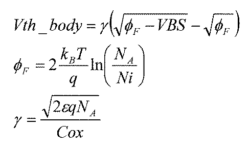
ここでkbはボルツマン定数、Tは温度、Niは真性キャリア密度である。不純物密度NAが温度依存性を持つためVth_bodyは温度に依存して変化することになる。
図5および図6に示す本願実施例ではVBS=0VなのでVth_sens_body=0Vとなり前述の相対誤差は本質的に生じない。よって図8Bに示す通り温度に依存した相対誤差はゼロとなり、余分な調整の手間を省くことが可能となり、安価で高精度なセンサを提供可能となる。
ここまでで、本願実施例により基板効果を取り除くことによる利点を述べた。次に、図9を用いて1/f雑音の低減効果を述べる。
ここまでで、本願実施例により基板効果を取り除くことによる利点を述べた。次に、図9を用いて1/f雑音の低減効果を述べる。
図9は、ある半導体製造プロセスFAB-Aで提供される標準NチャネルFETモデルTypNと標準PチャネルFETモデルTypPを用いて1/f雑音を計算し、PチャネルFETとNチャネルFETで比較したものである。計算にはBSIM3における1/f雑音計算式である下記の式(4)を用いた。
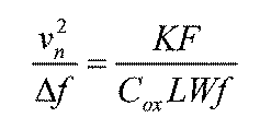
ここでvnはゲート入力換算ノイズ、Δfはバンド幅、KFは1/f雑音パラメータ、LはFETのゲート長、WはFETのゲート幅、fは測定周波数である。6sigma雑音を計算すると、FAB-Aにおける雑音レベルは検出対象が10ppm存在するときに出力に比較してNチャネル、Pチャネル共に2桁程度小さい。しかし、KF>1E-23である製造ラインを使った場合、1/f雑音の大きさが検出対象10ppmの信号出力と同程度となり、無視できない大きさとなる。
このとき、PチャネルFETにおける1/f雑音はNチャネルFETの1/2以下の大きさであるため、Pチャネル型はNチャネル型に比較して高精度化に有利となる。前述の通り1/f雑音はランダム雑音であるため参照FETとセンサFETの差分では除去不可能である。よって、センサチップレベルでできるだけ小さくすることが望ましい。また1/f雑音は計測時間が長くなるほど大きくなることからPチャネルFETでセンサFETと参照FETを構成することにより長時間動作に対する安定性や信頼性を向上させることも可能である。
図10を用いて次にPチャネルFETに特有の特徴について説明する。図10では検出対象ガスを検知した時の振る舞い(Gas detecting)と環境温度が上昇した時の振る舞い(Temperature rising)をPチャネルFET(PCH)とNチャネルFET(NCH)で比較して示した。温度範囲としては、例えばデバイスの動作可能な範囲内で、温度を上下させた場合を想定する。
まず検出対象ガスを検知した時のセンサFETの振る舞いについて説明する。図中点線はガスが存在しない時、実線はガスが存在するときのIDS-VGS特性を示している。NチャネルセンサFETでは検出対象ガス雰囲気中では閾電圧VTHが小さくなり、PチャネルセンサFETでは逆に大きくなる。ただしPチャネルセンサFETにおいてVTHが小さくなるとは、同じドレイン電流IDSを得る為に必要なゲートソース電圧VGSが小さくなることを意味する。
一方で環境温度上昇時には、温度上昇前と比較してNチャネルFETにおいてはVTHが減少し、PチャネルFETにおいてもVTHが減少する。点線が温度上昇前、実線が温度上昇後のIDS-VGS特性である。
NチャネルセンサFETではVTHの変化の方向が検出対象ガスの検出時と温度上昇時で同じである一方、PチャネルセンサFETでは逆である。検出対象ガスが温度上昇と共に発生する場合PチャネルセンサFETでは出力の方向が逆になることから検出対象ガスの検出によるVTH変化と温度上昇によるVTH変化を明確に分離することができる。一方でNチャネルセンサFETでは分離することが出来ない。FCVや原子力発電所など、検出対象ガスの発生に温度上昇を伴う応用に際しては、誤検知の可能性を低くできるという意味で、PチャネルセンサFETはNチャネルよりも有利となる。逆に、検出対象ガスの発生に温度低下を伴う場合にはNチャネルセンサFETの方がPチャネルよりも適すると言える。
以上がPチャネルFETで、センサFETと参照FETを構成することで得られる効果である。
図11には図6に示したセンサシステム(SENSORSYSTEM)におけるVTH検出回路(VTHSENSE)の具体的な構成の一例について述べる。一定のドレイン電流を生成するドレインソース電流生成回路(IDSGEN)の出力がセンサFET(SENSOR)向けソース電位(VSSEN)に接続される。ソース電圧バッファ(SBUF)はソース電位(VSSEN)を入力としセンサFETデバイス出力(VSEN)に入力と同じ電圧を出力する。これによりセンサFETデバイス出力(VSEN)の負荷が大きくてもソース電位(VSSEN)の電圧レベルを演算回路(CAL)まで伝送可能である。
ドレインソース電圧生成回路(VDSGEN)は電圧生成回路(VGEN)で生成されたセンサFET向けドレインソース電圧(VDSSEN)とセンサFETデバイス出力(VSEN)を入力として(VDS0)を出力する。(VDS0)の電圧はセンサFET向けドレインソース電圧(VDSSEN)と接地との差電圧をセンサFETデバイス出力(VSEN)を基準としてこれに足し合わせた大きさになる。すなわちVDS0=VSEN+VDSSENである。
センサFETデバイス出力(VSEN)はセンサFETのソース電位と等しいことからドレインソース電圧生成回路(VDSGEN)によりセンサFETのソースドレイン電圧は一定のセンサFET向けドレインソース電圧(VDSSEN)に維持されることになる。ドレイン電圧バッファ(DBUF)はセンサFET向けドレイン電位(VDSEN)に(VDS0)の電圧を出力する。これによりセンサFET向けドレイン電位(VDSEN)に大きな負荷が接続されている場合にも駆動が可能となる利点がある。VTH検出回路(VTHSENSE)とP型FETセンサチップ(PCHSENSORCHIP)が長いケーブルで接続されるような状況でもドレイン電圧バッファ(DBUF)によりセンサFETのドレインソース電圧は(VDS0)に維持される。参照FET(REFERENCE)側のVTH検出回路(VTHSENSE)も、基本的にセンサFET側と同様である。なお、図11中のオペアンプは一般的な特性を持つ市販オペアンプで構わない。
以下に第二の実施例について説明する。
図12はセンサチップの第二の実施例である。PチャネルセンサFETとPチャネル参照FETがP型基板(PSUB)上に形成される点は図5に示す第一の実施例と同じであるが、参照FETのゲートが検出対象に対して触媒作用を持たないゲート(GATE)で構成される点が異なる。本構成では図5に示す遮断膜(PASSI)の劣化により参照FETが検出対象に対して感度を持ってしまう不良を本質的に回避できる。しかし、触媒作用を持たないゲート(GATE)と触媒ゲート電極(CATGATE)の製膜を別々に行う必要があり、製膜プロセスコスト、マスク枚数が増大する。
図13はセンサシステムの第二の実施例である。図6に示す第一の実施例と比較してVTHセンシング回路(VTHSENSE)を1個に減らし、センサFETと参照FETでスイッチSWを介して一つのVTHセンシング回路(VTHSENSE)を共有する点が異なる。スイッチ制御信号(SWCTRL)は補正演算回路(CAL)により生成される。上記構成とすることでVTHセンシング回路(VTHSENSE)をセンサFETと参照FETに個別に設けた場合と比較して、回路のばらつきに起因する誤差を低減することができ、更に回路構成が簡単になるためコストが低減される。時分割でセンサFET出力と参照信号出力を交互に切り替えるため計測の同時性は失われる。しかし、ガス濃度の変化時定数よりも十分に早く切り替えを行うことで、この不利は解消される。具体的には1Hz以上の速度でスイッチングすれば計測精度に影響は出ない。
図14にはセンサチップの第三の実施例を示す。図5に示す第一の実施例にPN接合温度計(TEMPMETER)を追加した構成である。PN接合はPチャネルセンサFETとPチャネル参照FETと同じP型基板(PSUB)上に形成される。アノード端子(APN)はP拡散領域(P+)に接続され、カソード端子(CPN)はN拡散領域(N+)に接続される。センサFET、参照FET、PN接合のそれぞれのウェル(NWELL)は基板電位(SUB)を接地電位とすることで互いに電気的に分離される。
図14における参照FETのゲートは触媒ゲート電極(CATGATE)であるが図12に示したように触媒作用の無いゲート(GATE)としても良い。つまりPN接合温度計をセンサチップ上に設けることと参照FETの構成とは無関係である。
図15には図14のセンサチップを含む第三のセンサシステムの実施例を示す。図6と比較してセンサチップ上にPN接合で構成された温度計(TEMPMETER)が含まれる点、この温度計(TEMPMETER)を制御する回路ブロックが追加されている点が異なる。
電流源(IDIODEGEN)では温度計(TEMPMETER)に供給する電流を生成する。基準電圧生成回路(VGEN)では温度計(TEMPMETER)を適切に制御するための電圧(VDIODE)が生成される。温度計(TEMPMETER)のアノード電位(VF)を用い演算回路(CAL)でセンサチップの温度を得る。演算回路(CAL)では得られたチップ温度情報を用いて、チップ温度を一定に保つ制御やセンサ出力の感度補正演算を実施する。FET型ガスセンサは触媒金属に検出対象ガスが吸蔵されることで出力を得る為、チップ温度により感度が変化する。よってチップ上に温度計を設けて感度補正を行うことは、環境温度が変化する応用において信頼性を確保するために望ましい。
図16はセンサチップの第四の実施例である。図14に示した第三の実施例と比較して温度計(TEMPMETER)が配線抵抗により構成される。図16は配線抵抗全体のある一断面を示しており、実際には必要な長さの配線がチップ上に形成されているものとする。配線の一方の端をRH端子(RH)、もう一方の端をRL端子(RL)として取り出す。金属配線抵抗は温度の関数であるため、抵抗値を計測することでチップ温度の情報を得ることができる。上記の配線温度計はチップ温度を調整する電熱ヒータとして活用することも可能である。この際にはRH端子(RH)およびRL端子(RL)はヒータ電源の接続端子と抵抗測定端子を兼ねる。抵抗値を精度良く計測するためには4端子計測が望ましいため、RH端子(RH)をRH1とRH2、RL端子(RL)をRL1とRL2のように分けて用意する方法もある。図14の説明で述べたとおり、参照FETのゲートは非触媒ゲート(GATE)に置き換え、検知対象遮断膜(PASSI)を除いても良い。つまり図12に示したセンサチップの第二の実施例に配線抵抗温度計を適用した場合も本願の範囲に含まれる。
図17はセンサチップの第五の実施例である。図16に示した第四の実施例と比較して抵抗温度計(TEMPMETER)を拡散層抵抗で形成した点が異なる。配線抵抗温度計と比較して、安定性が高い利点がある。また高抵抗化が容易であるため、電熱ヒータとして活用した場合には発熱効率を高められるといった利点が考えられる。また配線がP型基板(PSUB)に埋め込まれる構成であるため配線抵抗温度計と比較してヒータとして活用した時の熱効率を向上可能である。電熱ヒータとして活用する場合にはRH端子(RH)およびRL端子(RL)はヒータ電源の接続端子と抵抗測定端子を兼ねる。抵抗値を精度良く計測するためには4端子計測が望ましいため、RH端子(RH)をRH1とRH2、RL端子(RL)をRL1とRL2のように分けて用意する方法もある。拡散層抵抗温度計は拡散層製造工程で同時に作ることが可能であるためプロセスコストの増加も抑えられる点が好ましい。図14の説明で述べたとおり、参照FETのゲートは非触媒ゲート(GATE)に置き換え、検知対象遮断膜(PASSI)を除いても良い。つまり図12に示したセンサチップの第二の実施例に拡散層抵抗温度計を適用した場合も本願の範囲に含まれる。
図18は図16と図17に示したセンサチップを用いたセンサシステムの第四のセンサシステムの実施例である。図15と比較して温度計(TEMPMETER)が抵抗で構成されている点が異なる。電流源(IRESGEN)は温度計(TEMPMETER)制御用の電流を生成する回路ブロックである。基準電圧生成回路(VGEN)では抵抗温度計制御用の電圧(VRES)が生成される。抵抗温度計出力(VR)は演算回路(CAL)に入力される。図15の説明で述べたとおり、チップ温度情報を含む抵抗温度計出力(VR)を用いてチップ温度の制御、センサ出力の補正演算を行うことで、高信頼化、高安定化を図ることができる。
図19はセンサチップの第六の実施例である。N型基板(NSUB)を用いる場合にはN型基板(NSUB)上にディープPウェル(DPWELL)を設け、更にその上にPチャネルセンサFETとPチャネル参照FETを形成する。ディープPウェル(DPWELL)を構成するプロセスコストが増大するがN型基板(NSUB)を用いなければならない応用には有効である。この際には基板電位(SUB)は接地ではない高電位にする必要がある点に注意を要する。
図20はN型基板(NSUB)上にPチャネルセンサFETとPチャネル参照FETをディープウェル無しに構成したセンサチップの第七の実施例である。センサFETのウェル電位と参照FETのウェル電位とを分離するため、トレンチ型素子分離(STI)を両者の間に設ける。これによりセンサFETのウェルと参照FETのウェル間のインピーダンスが増大するため、ウェル電位をそれぞれ独立に制御可能となり、結果としてソースとウェルを短絡して基板効果を無くす構成を実現できる。
図19、図20に明記しないが図12に示すように参照FETが非触媒ゲート(GATE)を有する場合や図14に示すPN接合温度計(TEMPMETER)を有する場合、図16に示す配線抵抗温度計(TEMPMETER)を有する場合、図17に示す拡散層抵抗(TEMPMETER)を有する場合も同様の派生実施例として本願の範囲に含まれるものとする。
1/f雑音の低減効果は期待できないが、ウェルとソースを短絡することで基板効果を無くす構成はNチャネルFETを用いた場合でも実現可能である。
図21は図5に示した第一の実施例に対してP型基板をN型基板(NSUB)に、PチャネルFETをNチャネルFETに置き換えた、第八の実施例である。
図22は図19に示した第六の実施例に対してN型基板をP型基板(PSUB)に、ディープPウェルをディープNウェル(DNWELL)に、PチャネルFETをNチャネルFETに置き換えた、第九の実施例である。
図23は図20に示した第七の実施例に対してN型基板をP型基板(PSUB)に、PチャネルFETをNチャネルFETに置き換えた、第十の実施例である。
図24は、図5に示したPチャネルFETで半導体素子を構成した場合の、断面構造図の一例である。P型基板(PSUB)に、Nウェル(NWELL)を形成し、その中にP型FETを形成する。センサFET(PCHSENSOR)、参照FET(PCHREFERENCE)ともに、触媒ゲート電極(SCATGATE,RCATGATE)を備えているが、センサFETの触媒ゲート電極(SCATGATE)が、遮断膜(PASSI)に形成されたスルーホールで露出しているのに対して、参照FETの触媒ゲート電極(RCATGATE)は、遮断膜(PASSI)に覆われている。触媒ゲート電極下には、ゲート酸化膜(OXIDE)が存在する。また、素子分離膜(OX1)、層間膜(OX2)がある。
参照FETのドレイン端子(DREF)はドレインパッド(DRAINPAD)に、参照FETのソース端子(SREF)はソースパッド(SREFPAD)に、参照FETのウェル端子(BREF)はボディパッド(BREFPAD)に、触媒ゲート電極(RCATGATE)はゲートパッド(RCATGATEPAD)に、基板(SUB)は基板電位パッド(SUBPAD)に、それぞれ接続されており、信号を入出力することができる。
センスFETのドレイン端子(DSEN)はドレインパッド(DRAINPAD)に、参照FETのソース端子(SSEN)はソースパッド(SSENPAD)に、参照FETのウェル端子(BSEN)はボディパッド(BSENPAD)に、触媒ゲート電極(SCATGATE)はゲートパッド(SCATGATEPAD)に、それぞれ接続されており、信号を入出力することができる。
なお、センサFET(PCHSENSOR)と参照FET(PCHREFERENCE)は、対比説明のために図24Aと図24Bに分けて示しているが、実際には、共通のP型基板(PSUB)上に形成されている。
第八から第十の実施例においても、明記しないが、参照FETのゲートを非触媒ゲート(GATE)で構成するパタンや、図14に示すPN接合温度計(TEMPMETER)を有する場合、図16に示す配線抵抗温度計(TEMPMETER)を有する場合、図17に示す拡散層抵抗(TEMPMETER)を有する場合も同様の派生実施例として本願の範囲に含まれるものとする。すなわち、本発明は上記した実施形態に限定されるものではなく、様々な変形例が含まれる。例えば、ある実施例の構成の一部を他の実施例の構成に置き換えることが可能であり、また、ある実施例の構成に他の実施例の構成を加えることが可能である。また、各実施例の構成の一部について、他の実施例の構成の追加・削除・置換をすることが可能である。
トランジスタの「ソース」や「ドレイン」の機能は、異なる極性のトランジスタを採用する場合や、回路動作において電流の方向が変化する場合などには入れ替わることがある。このため、本明細書においては、「ソース」や「ドレイン」の用語は、場合により入れ替えて用いることができる。
本明細書等において「電極」や「配線」の用語は、これらの構成要素を機能的に限定するものではない。例えば、「電極」は「配線」の一部として用いられることがあり、その逆もまた同様である。さらに、「電極」や「配線」の用語は、複数の「電極」や「配線」が一体となって形成されている場合なども含む。
本発明のFET型センサは、燃料電池自動車や水素ステーションといった水素インフラをはじめとして、各種プラントや原子力発電所の水素濃度計にも適用可能な技術である。
FET 電界効果トランジスタ
FCV 燃料電池自動車
VDS ドレインソース電圧
VG 接地電位を基準としたゲート電位
VREF 参照FETデバイス出力
PASSI 検出対象遮断膜
OXIDE ゲート酸化膜
CATGATE 触媒金属ゲート
DREF 参照FETのドレイン端子
SREF 参照FETのソース端子
BREF 参照FETのウェル端子
IDS ドレインソース電流
WELL ウェル
SUB 半導体基板
PSUB P型半導体基板
VSEN センサFETデバイス出力
DIPOLE 水素双極子
DSEN センサFETのドレイン端子
SSEN センサFETのソース端子
BSEN センサFETのウェル端子
DCTCIRCUIT 検出回路
VTHSENSE VTH検出回路
VDSEN センサFET向けドレイン電位
VSSEN センサFET向けソース電位
VDSSEN センサFET向けドレインソース電圧
VGEN 基準電圧生成回路
VDSREF 参照FET向けドレインソース電圧
VDREF 参照FET向けドレイン電位
VSREF 参照FET向けソース電位
CAL 補正演算回路
VDD High側電源電位
VBS 基板電圧
VGS ゲートソース電圧
VTH しきい電圧
GATE 非触媒ゲート
IDSGEN ドレインソース電流生成回路
SBUF ソース電圧バッファ
DBUF ドレイン電圧バッファ
VDSGEN ドレインソース電圧生成回路
SW 切り替えスイッチ
SWCTRL 切り替えスイッチ制御線
APN PN接合のアノード端子
CPN PN接合のカソード端子
TEMPMETER 温度計
VDIODE PN接合向け制御電圧
IDIODEGEN PN接合向け制御電流生成回路
VF PN接合温度計出力
RH 抵抗温度計向けハイ端子
RL 抵抗温度計向けロウ端子
VRES 抵抗温度計向け制御電圧
IRESGEN 抵抗温度計向け制御電流生成回路
DPWELL ディープPウェル
DNWELL ディープNウェル
STI トレンチ型素子分離
FCV 燃料電池自動車
VDS ドレインソース電圧
VG 接地電位を基準としたゲート電位
VREF 参照FETデバイス出力
PASSI 検出対象遮断膜
OXIDE ゲート酸化膜
CATGATE 触媒金属ゲート
DREF 参照FETのドレイン端子
SREF 参照FETのソース端子
BREF 参照FETのウェル端子
IDS ドレインソース電流
WELL ウェル
SUB 半導体基板
PSUB P型半導体基板
VSEN センサFETデバイス出力
DIPOLE 水素双極子
DSEN センサFETのドレイン端子
SSEN センサFETのソース端子
BSEN センサFETのウェル端子
DCTCIRCUIT 検出回路
VTHSENSE VTH検出回路
VDSEN センサFET向けドレイン電位
VSSEN センサFET向けソース電位
VDSSEN センサFET向けドレインソース電圧
VGEN 基準電圧生成回路
VDSREF 参照FET向けドレインソース電圧
VDREF 参照FET向けドレイン電位
VSREF 参照FET向けソース電位
CAL 補正演算回路
VDD High側電源電位
VBS 基板電圧
VGS ゲートソース電圧
VTH しきい電圧
GATE 非触媒ゲート
IDSGEN ドレインソース電流生成回路
SBUF ソース電圧バッファ
DBUF ドレイン電圧バッファ
VDSGEN ドレインソース電圧生成回路
SW 切り替えスイッチ
SWCTRL 切り替えスイッチ制御線
APN PN接合のアノード端子
CPN PN接合のカソード端子
TEMPMETER 温度計
VDIODE PN接合向け制御電圧
IDIODEGEN PN接合向け制御電流生成回路
VF PN接合温度計出力
RH 抵抗温度計向けハイ端子
RL 抵抗温度計向けロウ端子
VRES 抵抗温度計向け制御電圧
IRESGEN 抵抗温度計向け制御電流生成回路
DPWELL ディープPウェル
DNWELL ディープNウェル
STI トレンチ型素子分離
Claims (15)
- P型半導体基板と、
前記P型半導体基板に形成された第一のNウェル内にP型FETで形成された検知対象物に対して感応性を持つセンサFETと、
前記P型半導体基板に形成された第二のNウェル内にP型FETで形成された検知対象に対して感応性を持たない参照FETと、を有し、
前記第一のNウェルと前記第二のNウェルが電気的に分離され、
ガス雰囲気中における前記センサFETと前記参照FETの閾電圧の差分を検出する検出回路を有する、ことを特徴とするセンサシステム。 - 前記センサFETの閾電圧を計測する第一のソースフォロア回路と、
前記参照FETの閾電圧を計測する前記ソースフォロア回路とは独立して設けられた第二のソースフォロア回路とを有する、ことを特徴とする請求項1記載のセンサシステム。 - 前記センサFETの閾電圧と前記参照FETの閾電圧とを計測するソースフォロア回路を有し、
前記センサFETの閾電圧と前記参照FETの閾電圧とを計測するにあたっては、前記ソースフォロア回路と前記センサFET、もしくは、前記ソースフォロア回路と前記参照FETをスイッチングにより切り替えて接続する、ことを特徴とする請求項1記載のセンサシステム。 - 更に、前記P型半導体基板には温度測定のためのPN接合部を有する、ことを特徴とする請求項1記載のセンサシステム。
- 半導体基板と、
前記半導体基板に形成された第一のウェル内にFETで形成された検知対象に対して感応性をもつセンサFETと、
前記半導体基板に形成された第二のウェル内にFETで形成された検知対象に感応性を持たない参照FETと、を有し、
前記第一のウェルと前記第二のウェルとは電気的に分離して設けられ、
前記センサFETのソースと前記第一のウェルとが短絡されており、
前記参照FETのソースと前記第二のウェルとが短絡されており、
ガス雰囲気中における前記センサFETと前記参照FETの閾電圧の差分を検出する検出回路を有する
ことを特徴とするセンサシステム。
- 前記短絡されたセンサFETのウェル電位とソース電位に対して接続される、センサFET用ドレイン電流源と、
前記センサFETのソース電位を入力として、当該入力を前記検出回路に出力するセンサFET用ソース電圧バッファと、
前記センサFETのソースドレイン電圧を一定に維持する、センサFET用ソースドレイン電圧生成回路と、
前記短絡された参照FETのウェル電位とソース電位に対して接続される、参照FET用ドレイン電流源と、
前記参照FETのソース電位を入力として、当該入力を前記検出回路に出力する参照FET用ソース電圧バッファと、
前記参照FETのソースドレイン電圧を一定に維持する、参照FET用ソースドレイン電圧生成回路と、を有する、請求項5記載のセンサシステム。 - 同一の半導体基板に、
半導体領域と、
前記半導体領域に形成された第一のウェル内にFETで形成された、検知対象物に対して感応性を持つセンサFETと、
前記半導体領域に形成された第二のウェル内にFETで形成された、検知対象に対して感応性を持たない参照FETと
前記第一のウェルと前記第二のウェルの間の電気的導通を妨げる構成と、
前記センサFETの閾値電圧または閾値電圧の変化を示す信号を出力するセンサ信号出力端子と、
前記参照FETの閾電圧または閾値電圧の変化を示す信号を出力する参照信号出力端子と、
を有するセンサデバイス。 - 前記半導体領域が、第1導電型の半導体領域であり、
前記第一及び第二のウェルは、第2導電型のウェルであり、
前記第一及び第二の第2導電型ウェルの間を前記第1導電型の半導体領域で分離することにより、前記第一及び第二の第2導電型ウェルの間の電気的導通を妨げる、請求項7記載のセンサデバイス。
- 前記第一及び第二のウェルの間に、トレンチ型素子分離構造を設けることにより、前記第一及び第二のウェルの間の電気的導通を妨げる、請求項7記載のセンサデバイス。
- 前記半導体基板に、温度に対応した信号を発生する構造を設ける、請求項7記載のセンサデバイス。
- 前記温度に対応した信号を発生する構造として、PN接合を設ける、請求項10記載のセンサデバイス。
- 前記温度に対応した信号を発生する構造として、抵抗部材を設ける、請求項10記載のセンサデバイス。
- 前記センサFETのウェル電位とソース電位が短絡され、前記参照FETのウェル電位とソース電位が短絡されている、請求項7記載のセンサデバイス。
- 前記ウェル電位と短絡された前記センサFETのソース電位を前記センサ信号出力端子に出力し、前記ウェル電位と短絡された前記参照FETのソース電位を前記参照信号出力端子に出力する、請求項13記載のセンサデバイス。
- 前記半導体領域は、P型半導体領域であり、
前記第一及び第二のウェルは、N型半導体領域として形成され、
前記センサFET及び前記参照FETは、P型FETである、請求項7記載のセンサデバイス。
Priority Applications (3)
| Application Number | Priority Date | Filing Date | Title |
|---|---|---|---|
| EP15876971.1A EP3244200A4 (en) | 2015-01-09 | 2015-12-02 | Sensor system and device |
| US15/541,037 US10151725B2 (en) | 2015-01-09 | 2015-12-02 | Sensor system and device |
| CN201580069924.XA CN107110802B (zh) | 2015-01-09 | 2015-12-02 | 传感系统和器件 |
Applications Claiming Priority (2)
| Application Number | Priority Date | Filing Date | Title |
|---|---|---|---|
| JP2015003464A JP6425546B2 (ja) | 2015-01-09 | 2015-01-09 | 水素センサシステム |
| JP2015-003464 | 2015-01-09 |
Publications (1)
| Publication Number | Publication Date |
|---|---|
| WO2016111098A1 true WO2016111098A1 (ja) | 2016-07-14 |
Family
ID=56355801
Family Applications (1)
| Application Number | Title | Priority Date | Filing Date |
|---|---|---|---|
| PCT/JP2015/083889 Ceased WO2016111098A1 (ja) | 2015-01-09 | 2015-12-02 | センサシステムおよびデバイス |
Country Status (5)
| Country | Link |
|---|---|
| US (1) | US10151725B2 (ja) |
| EP (1) | EP3244200A4 (ja) |
| JP (1) | JP6425546B2 (ja) |
| CN (1) | CN107110802B (ja) |
| WO (1) | WO2016111098A1 (ja) |
Families Citing this family (8)
| Publication number | Priority date | Publication date | Assignee | Title |
|---|---|---|---|---|
| CN108152336B (zh) * | 2017-12-12 | 2020-04-28 | 杭州电子科技大学 | 一种具有气体传感功能的二维材料源跟随器 |
| US11293897B2 (en) | 2018-11-30 | 2022-04-05 | Taiwan Semiconductor Manufacturing Company, Ltd. | High sensitivity ISFET sensor |
| US10830799B1 (en) * | 2019-07-12 | 2020-11-10 | Alpha And Omega Semiconductor (Cayman) Ltd. | Temperature and VGS compensation for current sensing using Rdson in MOSFETS |
| CN112968001A (zh) * | 2019-12-13 | 2021-06-15 | 深圳第三代半导体研究院 | 一种基于氮化镓/铝镓氮异质结的电压传感器及制备方法 |
| CN112798126B (zh) * | 2021-04-08 | 2021-07-02 | 成都蓉矽半导体有限公司 | 一种高灵敏度的碳化硅可集成温度传感器 |
| US12055565B2 (en) | 2022-11-22 | 2024-08-06 | Alpha And Omega Semiconductor International Lp | Linear discrete Rdson temperature VGS compensation |
| WO2025080262A1 (en) * | 2023-10-10 | 2025-04-17 | Serinus Labs, Inc. | Dielectric adhesion layer for stability of gas sensitive noble metal film |
| JP2025090435A (ja) * | 2023-12-05 | 2025-06-17 | 株式会社日立ハイテク | ガスセンサモジュール |
Citations (7)
| Publication number | Priority date | Publication date | Assignee | Title |
|---|---|---|---|---|
| JPS63171351A (ja) * | 1987-01-09 | 1988-07-15 | Seitai Kinou Riyou Kagakuhin Shinseizou Gijutsu Kenkyu Kumiai | 差動型電界効果トランジスタ酸素センサ |
| US4874499A (en) * | 1988-05-23 | 1989-10-17 | Massachusetts Institute Of Technology | Electrochemical microsensors and method of making such sensors |
| JPH0293357A (ja) * | 1988-09-30 | 1990-04-04 | Toshiba Corp | 半導体湿度センサ |
| JPH0333646A (ja) * | 1989-06-30 | 1991-02-13 | Hitachi Ltd | 半導体化学センサ |
| WO2011055605A1 (ja) * | 2009-11-06 | 2011-05-12 | 株式会社日立製作所 | ガスセンサ |
| JP2012073154A (ja) * | 2010-09-29 | 2012-04-12 | Hitachi Ltd | ガスセンサおよびその製造方法 |
| JP2013064746A (ja) * | 2006-12-14 | 2013-04-11 | Life Technologies Corp | 大規模fetアレイを用いた分析物測定のための方法および装置 |
Family Cites Families (3)
| Publication number | Priority date | Publication date | Assignee | Title |
|---|---|---|---|---|
| US8120135B2 (en) * | 2004-05-19 | 2012-02-21 | Infineon Technologies Ag | Transistor |
| US8262900B2 (en) * | 2006-12-14 | 2012-09-11 | Life Technologies Corporation | Methods and apparatus for measuring analytes using large scale FET arrays |
| JP4296356B1 (ja) * | 2008-09-12 | 2009-07-15 | 国立大学法人 岡山大学 | ガスセンサ |
-
2015
- 2015-01-09 JP JP2015003464A patent/JP6425546B2/ja active Active
- 2015-12-02 WO PCT/JP2015/083889 patent/WO2016111098A1/ja not_active Ceased
- 2015-12-02 EP EP15876971.1A patent/EP3244200A4/en not_active Withdrawn
- 2015-12-02 US US15/541,037 patent/US10151725B2/en active Active
- 2015-12-02 CN CN201580069924.XA patent/CN107110802B/zh active Active
Patent Citations (7)
| Publication number | Priority date | Publication date | Assignee | Title |
|---|---|---|---|---|
| JPS63171351A (ja) * | 1987-01-09 | 1988-07-15 | Seitai Kinou Riyou Kagakuhin Shinseizou Gijutsu Kenkyu Kumiai | 差動型電界効果トランジスタ酸素センサ |
| US4874499A (en) * | 1988-05-23 | 1989-10-17 | Massachusetts Institute Of Technology | Electrochemical microsensors and method of making such sensors |
| JPH0293357A (ja) * | 1988-09-30 | 1990-04-04 | Toshiba Corp | 半導体湿度センサ |
| JPH0333646A (ja) * | 1989-06-30 | 1991-02-13 | Hitachi Ltd | 半導体化学センサ |
| JP2013064746A (ja) * | 2006-12-14 | 2013-04-11 | Life Technologies Corp | 大規模fetアレイを用いた分析物測定のための方法および装置 |
| WO2011055605A1 (ja) * | 2009-11-06 | 2011-05-12 | 株式会社日立製作所 | ガスセンサ |
| JP2012073154A (ja) * | 2010-09-29 | 2012-04-12 | Hitachi Ltd | ガスセンサおよびその製造方法 |
Non-Patent Citations (2)
| Title |
|---|
| KEIJI TSUKADA ET AL.: "Dual-Gate Field-Effect Transistor Hydrogen Gas Sensor with Thermal Compensation", JAPANESE JOURNAL OF APPLIED PHYSICS, vol. 49, 22 February 2010 (2010-02-22), pages 024206, XP001554139 * |
| See also references of EP3244200A4 * |
Also Published As
| Publication number | Publication date |
|---|---|
| CN107110802B (zh) | 2019-10-11 |
| JP2016128783A (ja) | 2016-07-14 |
| JP6425546B2 (ja) | 2018-11-21 |
| CN107110802A (zh) | 2017-08-29 |
| EP3244200A4 (en) | 2018-09-12 |
| EP3244200A1 (en) | 2017-11-15 |
| US20170370875A1 (en) | 2017-12-28 |
| US10151725B2 (en) | 2018-12-11 |
Similar Documents
| Publication | Publication Date | Title |
|---|---|---|
| JP6425546B2 (ja) | 水素センサシステム | |
| JP5547429B2 (ja) | 半導体装置 | |
| US9518953B2 (en) | Ion sensitive detector | |
| US8283704B2 (en) | Gas sensor | |
| JP6731846B2 (ja) | 電荷検出のための集積センサデバイス | |
| US20140234981A1 (en) | Double gate ion sensitive field effect transistor | |
| JP2015035578A (ja) | 半導体装置 | |
| TWI420123B (zh) | 具有偵測製程邊界角與極端溫度之電路 | |
| JP2006302977A (ja) | パワー半導体デバイスの温度計測装置 | |
| US20250314536A1 (en) | Temperature monitoring device manufacturing method | |
| US6948847B2 (en) | Temperature sensor for a MOS circuit configuration | |
| US9719959B2 (en) | Hydrogen ion sensor | |
| JP2018115888A (ja) | Fet型ガスセンサ及びガスセンサの制御方法 | |
| CN210895161U (zh) | 电子设备 | |
| US20090129440A1 (en) | Sensor | |
| US9829543B2 (en) | Sensor arrangement having thermo-EMF compensation | |
| JP5594407B2 (ja) | 半導体装置 | |
| JP2007225398A (ja) | 熱型赤外線検出器および熱型赤外線センサ | |
| TWI856920B (zh) | 半導體元件 | |
| CN1325922C (zh) | N型差分式电场微传感器 | |
| JP2007240157A (ja) | 半導体温度センサ回路,半導体集積回路および半導体温度センサ回路の調整方法 | |
| JPS5930029A (ja) | 温度検出装置 |
Legal Events
| Date | Code | Title | Description |
|---|---|---|---|
| 121 | Ep: the epo has been informed by wipo that ep was designated in this application |
Ref document number: 15876971 Country of ref document: EP Kind code of ref document: A1 |
|
| REEP | Request for entry into the european phase |
Ref document number: 2015876971 Country of ref document: EP |
|
| WWE | Wipo information: entry into national phase |
Ref document number: 15541037 Country of ref document: US |
|
| NENP | Non-entry into the national phase |
Ref country code: DE |