WO2016111144A1 - 有機電子素子の製造方法 - Google Patents
有機電子素子の製造方法 Download PDFInfo
- Publication number
- WO2016111144A1 WO2016111144A1 PCT/JP2015/085555 JP2015085555W WO2016111144A1 WO 2016111144 A1 WO2016111144 A1 WO 2016111144A1 JP 2015085555 W JP2015085555 W JP 2015085555W WO 2016111144 A1 WO2016111144 A1 WO 2016111144A1
- Authority
- WO
- WIPO (PCT)
- Prior art keywords
- organic
- substrate
- organic electronic
- layer
- film
- Prior art date
- Legal status (The legal status is an assumption and is not a legal conclusion. Google has not performed a legal analysis and makes no representation as to the accuracy of the status listed.)
- Ceased
Links
Images




Classifications
-
- H—ELECTRICITY
- H10—SEMICONDUCTOR DEVICES; ELECTRIC SOLID-STATE DEVICES NOT OTHERWISE PROVIDED FOR
- H10K—ORGANIC ELECTRIC SOLID-STATE DEVICES
- H10K71/00—Manufacture or treatment specially adapted for the organic devices covered by this subclass
- H10K71/10—Deposition of organic active material
-
- H—ELECTRICITY
- H10—SEMICONDUCTOR DEVICES; ELECTRIC SOLID-STATE DEVICES NOT OTHERWISE PROVIDED FOR
- H10K—ORGANIC ELECTRIC SOLID-STATE DEVICES
- H10K71/00—Manufacture or treatment specially adapted for the organic devices covered by this subclass
- H10K71/10—Deposition of organic active material
- H10K71/12—Deposition of organic active material using liquid deposition, e.g. spin coating
- H10K71/13—Deposition of organic active material using liquid deposition, e.g. spin coating using printing techniques, e.g. ink-jet printing or screen printing
-
- H—ELECTRICITY
- H10—SEMICONDUCTOR DEVICES; ELECTRIC SOLID-STATE DEVICES NOT OTHERWISE PROVIDED FOR
- H10D—INORGANIC ELECTRIC SEMICONDUCTOR DEVICES
- H10D30/00—Field-effect transistors [FET]
- H10D30/60—Insulated-gate field-effect transistors [IGFET]
- H10D30/67—Thin-film transistors [TFT]
-
- H—ELECTRICITY
- H10—SEMICONDUCTOR DEVICES; ELECTRIC SOLID-STATE DEVICES NOT OTHERWISE PROVIDED FOR
- H10K—ORGANIC ELECTRIC SOLID-STATE DEVICES
- H10K10/00—Organic devices specially adapted for rectifying, amplifying, oscillating or switching; Organic capacitors or resistors having potential barriers
-
- H—ELECTRICITY
- H10—SEMICONDUCTOR DEVICES; ELECTRIC SOLID-STATE DEVICES NOT OTHERWISE PROVIDED FOR
- H10K—ORGANIC ELECTRIC SOLID-STATE DEVICES
- H10K30/00—Organic devices sensitive to infrared radiation, light, electromagnetic radiation of shorter wavelength or corpuscular radiation
-
- H—ELECTRICITY
- H10—SEMICONDUCTOR DEVICES; ELECTRIC SOLID-STATE DEVICES NOT OTHERWISE PROVIDED FOR
- H10K—ORGANIC ELECTRIC SOLID-STATE DEVICES
- H10K50/00—Organic light-emitting devices
-
- H—ELECTRICITY
- H10—SEMICONDUCTOR DEVICES; ELECTRIC SOLID-STATE DEVICES NOT OTHERWISE PROVIDED FOR
- H10K—ORGANIC ELECTRIC SOLID-STATE DEVICES
- H10K71/00—Manufacture or treatment specially adapted for the organic devices covered by this subclass
-
- H—ELECTRICITY
- H10—SEMICONDUCTOR DEVICES; ELECTRIC SOLID-STATE DEVICES NOT OTHERWISE PROVIDED FOR
- H10K—ORGANIC ELECTRIC SOLID-STATE DEVICES
- H10K71/00—Manufacture or treatment specially adapted for the organic devices covered by this subclass
- H10K71/10—Deposition of organic active material
- H10K71/191—Deposition of organic active material characterised by provisions for the orientation or alignment of the layer to be deposited
-
- H—ELECTRICITY
- H10—SEMICONDUCTOR DEVICES; ELECTRIC SOLID-STATE DEVICES NOT OTHERWISE PROVIDED FOR
- H10K—ORGANIC ELECTRIC SOLID-STATE DEVICES
- H10K77/00—Constructional details of devices covered by this subclass and not covered by groups H10K10/80, H10K30/80, H10K50/80 or H10K59/80
- H10K77/10—Substrates, e.g. flexible substrates
- H10K77/111—Flexible substrates
-
- H—ELECTRICITY
- H10—SEMICONDUCTOR DEVICES; ELECTRIC SOLID-STATE DEVICES NOT OTHERWISE PROVIDED FOR
- H10W—GENERIC PACKAGES, INTERCONNECTIONS, CONNECTORS OR OTHER CONSTRUCTIONAL DETAILS OF DEVICES COVERED BY CLASS H10
- H10W72/00—Interconnections or connectors in packages
- H10W72/01—Manufacture or treatment
- H10W72/0198—Manufacture or treatment batch processes
-
- B—PERFORMING OPERATIONS; TRANSPORTING
- B05—SPRAYING OR ATOMISING IN GENERAL; APPLYING FLUENT MATERIALS TO SURFACES, IN GENERAL
- B05D—PROCESSES FOR APPLYING FLUENT MATERIALS TO SURFACES, IN GENERAL
- B05D1/00—Processes for applying liquids or other fluent materials
- B05D1/26—Processes for applying liquids or other fluent materials performed by applying the liquid or other fluent material from an outlet device in contact with, or almost in contact with, the surface
-
- B—PERFORMING OPERATIONS; TRANSPORTING
- B05—SPRAYING OR ATOMISING IN GENERAL; APPLYING FLUENT MATERIALS TO SURFACES, IN GENERAL
- B05D—PROCESSES FOR APPLYING FLUENT MATERIALS TO SURFACES, IN GENERAL
- B05D2201/00—Polymeric substrate or laminate
-
- B—PERFORMING OPERATIONS; TRANSPORTING
- B05—SPRAYING OR ATOMISING IN GENERAL; APPLYING FLUENT MATERIALS TO SURFACES, IN GENERAL
- B05D—PROCESSES FOR APPLYING FLUENT MATERIALS TO SURFACES, IN GENERAL
- B05D2252/00—Sheets
- B05D2252/02—Sheets of indefinite length
-
- H—ELECTRICITY
- H10—SEMICONDUCTOR DEVICES; ELECTRIC SOLID-STATE DEVICES NOT OTHERWISE PROVIDED FOR
- H10K—ORGANIC ELECTRIC SOLID-STATE DEVICES
- H10K10/00—Organic devices specially adapted for rectifying, amplifying, oscillating or switching; Organic capacitors or resistors having potential barriers
- H10K10/40—Organic transistors
-
- H—ELECTRICITY
- H10—SEMICONDUCTOR DEVICES; ELECTRIC SOLID-STATE DEVICES NOT OTHERWISE PROVIDED FOR
- H10K—ORGANIC ELECTRIC SOLID-STATE DEVICES
- H10K30/00—Organic devices sensitive to infrared radiation, light, electromagnetic radiation of shorter wavelength or corpuscular radiation
- H10K30/50—Photovoltaic [PV] devices
-
- H—ELECTRICITY
- H10—SEMICONDUCTOR DEVICES; ELECTRIC SOLID-STATE DEVICES NOT OTHERWISE PROVIDED FOR
- H10K—ORGANIC ELECTRIC SOLID-STATE DEVICES
- H10K50/00—Organic light-emitting devices
- H10K50/10—OLEDs or polymer light-emitting diodes [PLED]
-
- Y—GENERAL TAGGING OF NEW TECHNOLOGICAL DEVELOPMENTS; GENERAL TAGGING OF CROSS-SECTIONAL TECHNOLOGIES SPANNING OVER SEVERAL SECTIONS OF THE IPC; TECHNICAL SUBJECTS COVERED BY FORMER USPC CROSS-REFERENCE ART COLLECTIONS [XRACs] AND DIGESTS
- Y02—TECHNOLOGIES OR APPLICATIONS FOR MITIGATION OR ADAPTATION AGAINST CLIMATE CHANGE
- Y02E—REDUCTION OF GREENHOUSE GAS [GHG] EMISSIONS, RELATED TO ENERGY GENERATION, TRANSMISSION OR DISTRIBUTION
- Y02E10/00—Energy generation through renewable energy sources
- Y02E10/50—Photovoltaic [PV] energy
- Y02E10/549—Organic PV cells
-
- Y—GENERAL TAGGING OF NEW TECHNOLOGICAL DEVELOPMENTS; GENERAL TAGGING OF CROSS-SECTIONAL TECHNOLOGIES SPANNING OVER SEVERAL SECTIONS OF THE IPC; TECHNICAL SUBJECTS COVERED BY FORMER USPC CROSS-REFERENCE ART COLLECTIONS [XRACs] AND DIGESTS
- Y02—TECHNOLOGIES OR APPLICATIONS FOR MITIGATION OR ADAPTATION AGAINST CLIMATE CHANGE
- Y02P—CLIMATE CHANGE MITIGATION TECHNOLOGIES IN THE PRODUCTION OR PROCESSING OF GOODS
- Y02P70/00—Climate change mitigation technologies in the production process for final industrial or consumer products
- Y02P70/50—Manufacturing or production processes characterised by the final manufactured product
Definitions
- an object of the present invention is to provide a method for manufacturing an organic electronic device capable of reducing non-uniformity of the coating film thickness.
- the tensile force (tension) of the base material described above may be in a form of 20N or more and 150N or less. According to this aspect, since wrinkles and sagging in the transport direction do not occur in the film itself being transported when entering the air levitation stage, it is possible to form a stable and uniform coating film in a state where vertical vibration is suppressed. Become.
- the conveyance speed of the film substrate 110 is, for example, 2 m / min. 6 m / min.
- the tension set below and applied in the conveying direction of the film substrate 110 is set to, for example, 20N to 150N, preferably 30N to 100N. Note that the tension (tensile force) applied in the transport direction of the film substrate 110 may be adjusted by a tension adjusting mechanism (not shown).
- the air levitation stage 20 is used not for conveying the film base 110 but for floating the part where the film base 110 hangs down by its own weight. Thus, a relatively large amount of air generated by relatively large holes formed by processing is too strong. According to the air levitation stage 20 of the present embodiment, the amount of the film base 110 that hangs down by its own weight can be levitated by a relatively small amount of air generated by the relatively small holes of the porous material. .
- various conditions such as the air blowing flow rate, the number, size, and the interval of the air levitation stage, the interval between the air levitation stage and the film substrate, and the tension applied in the transport direction of the film substrate are exemplified.
- These assume a PEN film substrate having a thickness of 125 ⁇ m and a width of 320 mm.
- the upper and lower vibration amount of the film base material is 70 ⁇ m or less, in other words, the upper and lower displacement amount is ⁇ 35 ⁇ m or less. What is necessary is just to change these conditions suitably.
Landscapes
- Engineering & Computer Science (AREA)
- Manufacturing & Machinery (AREA)
- Physics & Mathematics (AREA)
- Electromagnetism (AREA)
- Optics & Photonics (AREA)
- Electroluminescent Light Sources (AREA)
- Thin Film Transistor (AREA)
- Photovoltaic Devices (AREA)
Abstract
Description
[検証1]
[検証2]
エア吹き出し流量:3×10⁻⁴L/(cm2・sec.)(風速換算:0.003m/sec.)
エア浮上ステージ20とフィルム基材110との間隔:50μm
また、その他の共通の検証条件は以下の通りであった。
フィルム基材110の搬送速度:6m/min.
フィルム基材110の搬送方向に加えられるテンション:30N
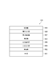
a)陽極/発光層/陰極
b)陽極/正孔注入層/発光層/陰極
c)陽極/正孔注入層/発光層/電子注入層/陰極
d)陽極/正孔注入層/発光層/電子輸送層/電子注入層/陰極
e)陽極/正孔注入層/正孔輸送層/発光層/陰極
f)陽極/正孔注入層/正孔輸送層/発光層/電子注入層/陰極
g)陽極/正孔注入層/正孔輸送層/発光層/電子輸送層/電子注入層/陰極
h)陽極/発光層/電子注入層/陰極
i)陽極/発光層/電子輸送層/電子注入層/陰極
ここで、記号「/」は、記号「/」を挟む各層が隣接して積層されていることを示す。
Claims (10)
- 有機材料を含む機能層を有する有機電子素子の製造方法であって、
ロールツーロール方式を用いて、可撓性を有する基材を水平搬送し、前記基材の上方に配置されたスリットコート塗布器によって、前記有機材料を含む塗布液を前記基材に塗布して、前記機能層を形成する塗布工程を有し、
前記塗布工程では、前記基材の下方に配置されたエア浮上ステージによって、前記基材をエア浮上させて、前記塗布液を前記基材に塗布する、
有機電子素子の製造方法。 - 前記エア浮上ステージは、多孔質材料からなる、請求項1に記載の有機電子素子の製造方法。
- 前記基材の上下の振動量は、70μm以下である、請求項1又は2に記載の有機電子素子の製造方法。
- 前記エア浮上ステージと前記基材との間隔は、30μm以上1mm以下である、請求項3に記載の有機電子素子の製造方法。
- 前記塗布液の粘度は、1cp以上20cp以下である、請求項3に記載の有機電子素子の製造方法。
- 前記基材の引張力は、20N以上150N以下である、請求項3に記載の有機電子素子の製造方法。
- 前記エア浮上ステージによるエアの風速は、0.001m/sec.以上0.3m/sec.以下である、請求項3に記載の有機電子素子の製造方法。
- 前記有機電子素子は有機EL素子である、請求項1~7の何れか1項に記載の有機電子素子の製造方法。
- 前記有機電子素子は有機太陽電池である、請求項1~7の何れか1項に記載の有機電子素子の製造方法。
- 前記有機電子素子は有機トランジスタである、請求項1~7の何れか1項に記載の有機電子素子の製造方法。
Priority Applications (4)
| Application Number | Priority Date | Filing Date | Title |
|---|---|---|---|
| EP15877017.2A EP3244701A4 (en) | 2015-01-07 | 2015-12-18 | Method for manufacturing organic electronic element |
| US15/541,599 US10319909B2 (en) | 2015-01-07 | 2015-12-18 | Method for manufacturing organic electronic element |
| KR1020177021432A KR20170101980A (ko) | 2015-01-07 | 2015-12-18 | 유기 전자 소자의 제조 방법 |
| CN201580072619.6A CN107211501B (zh) | 2015-01-07 | 2015-12-18 | 有机电子元件的制造方法 |
Applications Claiming Priority (2)
| Application Number | Priority Date | Filing Date | Title |
|---|---|---|---|
| JP2015001583A JP5799181B1 (ja) | 2015-01-07 | 2015-01-07 | 有機電子素子の製造方法 |
| JP2015-001583 | 2015-01-07 |
Publications (1)
| Publication Number | Publication Date |
|---|---|
| WO2016111144A1 true WO2016111144A1 (ja) | 2016-07-14 |
Family
ID=54348664
Family Applications (1)
| Application Number | Title | Priority Date | Filing Date |
|---|---|---|---|
| PCT/JP2015/085555 Ceased WO2016111144A1 (ja) | 2015-01-07 | 2015-12-18 | 有機電子素子の製造方法 |
Country Status (6)
| Country | Link |
|---|---|
| US (1) | US10319909B2 (ja) |
| EP (1) | EP3244701A4 (ja) |
| JP (1) | JP5799181B1 (ja) |
| KR (1) | KR20170101980A (ja) |
| CN (1) | CN107211501B (ja) |
| WO (1) | WO2016111144A1 (ja) |
Cited By (1)
| Publication number | Priority date | Publication date | Assignee | Title |
|---|---|---|---|---|
| US10686162B2 (en) | 2015-01-07 | 2020-06-16 | Sumitomo Chemical Company, Limited | Method for manufacturing organic EL panel |
Families Citing this family (4)
| Publication number | Priority date | Publication date | Assignee | Title |
|---|---|---|---|---|
| JP2017195115A (ja) * | 2016-04-21 | 2017-10-26 | 住友化学株式会社 | 有機el素子の製造方法 |
| KR102458991B1 (ko) * | 2018-03-30 | 2022-10-25 | 제이에프이 스틸 가부시키가이샤 | 방향성 전기 강판의 제조 방법 및 연속 성막 장치 |
| KR102611146B1 (ko) * | 2021-06-28 | 2023-12-06 | 세메스 주식회사 | 기판 처리 장치의 예열 방법 및 이를 위한 컴퓨터 프로그램 |
| CN120857832A (zh) * | 2025-07-21 | 2025-10-28 | 浙江大学 | 一种有机半导体单晶薄膜及其制备方法和用途 |
Citations (8)
| Publication number | Priority date | Publication date | Assignee | Title |
|---|---|---|---|---|
| JP2004131215A (ja) * | 2002-10-09 | 2004-04-30 | Ushio Inc | 帯状ワークの搬送装置 |
| JP2004335492A (ja) * | 2003-03-07 | 2004-11-25 | Junji Kido | 有機電子材料の塗布装置およびそれを使用した有機電子素子の製造方法 |
| US20090031579A1 (en) * | 2007-07-31 | 2009-02-05 | Piatt Michael J | Micro-structured drying for inkjet printers |
| JP2010140705A (ja) * | 2008-12-10 | 2010-06-24 | Konica Minolta Holdings Inc | 有機エレクトロルミネッセンスパネル及びその製造方法、該有機エレクトロルミネッセンスパネルを用いた照明装置、表示装置 |
| WO2012039218A1 (ja) * | 2010-09-25 | 2012-03-29 | コニカミノルタホールディングス株式会社 | 塗布方法、有機エレクトロニクス素子の製造方法 |
| WO2012172919A1 (ja) * | 2011-06-14 | 2012-12-20 | コニカミノルタホールディングス株式会社 | 有機エレクトロルミネッセンス素子の製造方法 |
| JP2014180603A (ja) * | 2013-03-18 | 2014-09-29 | Toray Ind Inc | 塗布装置、塗布方法およびディスプレイ用部材の製造方法 |
| JP2015022836A (ja) * | 2013-07-17 | 2015-02-02 | セーレン株式会社 | インクジェット記録装置 |
Family Cites Families (18)
| Publication number | Priority date | Publication date | Assignee | Title |
|---|---|---|---|---|
| JPS6436077U (ja) * | 1987-08-28 | 1989-03-06 | ||
| US5136966A (en) | 1988-10-28 | 1992-08-11 | Konica Corporation | Web coating apparatus |
| JP2724400B2 (ja) * | 1989-02-13 | 1998-03-09 | コニカ株式会社 | ウエブ塗布装置 |
| JP2724398B2 (ja) * | 1989-02-13 | 1998-03-09 | コニカ株式会社 | ウエブ塗布装置 |
| JP4129861B2 (ja) * | 2002-08-02 | 2008-08-06 | 大日本印刷株式会社 | 塗工装置 |
| JP4767251B2 (ja) * | 2004-04-14 | 2011-09-07 | コアフロー サイエンティフィック ソリューションズ リミテッド | 光学検査装置を平坦な対象物の接面に対して焦点合わせする方法 |
| KR101296659B1 (ko) | 2008-11-14 | 2013-08-14 | 엘지디스플레이 주식회사 | 세정 장치 |
| JP5418505B2 (ja) * | 2009-02-03 | 2014-02-19 | コニカミノルタ株式会社 | 有機エレクトロニクス素子及びその製造方法 |
| JP5831228B2 (ja) * | 2009-05-09 | 2015-12-09 | コニカミノルタ株式会社 | 塗布方法 |
| JP2012192332A (ja) | 2011-03-16 | 2012-10-11 | Toray Ind Inc | 塗布装置、塗布方法およびディスプレイ用部材の製造方法 |
| KR20130003560A (ko) * | 2011-06-30 | 2013-01-09 | 주식회사 에스에프에이 | 인쇄장치 |
| JP2013016405A (ja) * | 2011-07-06 | 2013-01-24 | Konica Minolta Holdings Inc | 有機エレクトロニクスデバイスおよびその製造方法 |
| CN106919003B (zh) | 2011-11-04 | 2018-10-16 | 株式会社尼康 | 图案形成方法及装置、图案曝光方法、以及元件制造方法 |
| JP5494899B2 (ja) * | 2012-04-09 | 2014-05-21 | 三菱化学株式会社 | 有機電界発光素子用組成物及び有機電界発光素子 |
| JP2014079708A (ja) * | 2012-10-17 | 2014-05-08 | Tokyo Ohka Kogyo Co Ltd | 両面塗布装置 |
| JP6036249B2 (ja) * | 2012-12-11 | 2016-11-30 | コニカミノルタ株式会社 | 有機エレクトロルミネッセンス素子の製造方法 |
| JP2014120350A (ja) * | 2012-12-17 | 2014-06-30 | Konica Minolta Inc | 有機エレクトロルミネッセンス素子の製造方法 |
| JP6254108B2 (ja) | 2015-01-07 | 2017-12-27 | 住友化学株式会社 | 有機elパネルの製造方法 |
-
2015
- 2015-01-07 JP JP2015001583A patent/JP5799181B1/ja not_active Expired - Fee Related
- 2015-12-18 CN CN201580072619.6A patent/CN107211501B/zh not_active Expired - Fee Related
- 2015-12-18 WO PCT/JP2015/085555 patent/WO2016111144A1/ja not_active Ceased
- 2015-12-18 KR KR1020177021432A patent/KR20170101980A/ko not_active Ceased
- 2015-12-18 EP EP15877017.2A patent/EP3244701A4/en not_active Ceased
- 2015-12-18 US US15/541,599 patent/US10319909B2/en not_active Expired - Fee Related
Patent Citations (8)
| Publication number | Priority date | Publication date | Assignee | Title |
|---|---|---|---|---|
| JP2004131215A (ja) * | 2002-10-09 | 2004-04-30 | Ushio Inc | 帯状ワークの搬送装置 |
| JP2004335492A (ja) * | 2003-03-07 | 2004-11-25 | Junji Kido | 有機電子材料の塗布装置およびそれを使用した有機電子素子の製造方法 |
| US20090031579A1 (en) * | 2007-07-31 | 2009-02-05 | Piatt Michael J | Micro-structured drying for inkjet printers |
| JP2010140705A (ja) * | 2008-12-10 | 2010-06-24 | Konica Minolta Holdings Inc | 有機エレクトロルミネッセンスパネル及びその製造方法、該有機エレクトロルミネッセンスパネルを用いた照明装置、表示装置 |
| WO2012039218A1 (ja) * | 2010-09-25 | 2012-03-29 | コニカミノルタホールディングス株式会社 | 塗布方法、有機エレクトロニクス素子の製造方法 |
| WO2012172919A1 (ja) * | 2011-06-14 | 2012-12-20 | コニカミノルタホールディングス株式会社 | 有機エレクトロルミネッセンス素子の製造方法 |
| JP2014180603A (ja) * | 2013-03-18 | 2014-09-29 | Toray Ind Inc | 塗布装置、塗布方法およびディスプレイ用部材の製造方法 |
| JP2015022836A (ja) * | 2013-07-17 | 2015-02-02 | セーレン株式会社 | インクジェット記録装置 |
Non-Patent Citations (1)
| Title |
|---|
| See also references of EP3244701A4 * |
Cited By (1)
| Publication number | Priority date | Publication date | Assignee | Title |
|---|---|---|---|---|
| US10686162B2 (en) | 2015-01-07 | 2020-06-16 | Sumitomo Chemical Company, Limited | Method for manufacturing organic EL panel |
Also Published As
| Publication number | Publication date |
|---|---|
| US20180006222A1 (en) | 2018-01-04 |
| EP3244701A4 (en) | 2018-10-03 |
| JP5799181B1 (ja) | 2015-10-21 |
| CN107211501B (zh) | 2020-01-07 |
| JP2016126964A (ja) | 2016-07-11 |
| EP3244701A1 (en) | 2017-11-15 |
| US10319909B2 (en) | 2019-06-11 |
| KR20170101980A (ko) | 2017-09-06 |
| CN107211501A (zh) | 2017-09-26 |
Similar Documents
| Publication | Publication Date | Title |
|---|---|---|
| JP5799181B1 (ja) | 有機電子素子の製造方法 | |
| JP5522170B2 (ja) | 塗布方法 | |
| JP5831228B2 (ja) | 塗布方法 | |
| US11342130B2 (en) | Method of making a photovoltaic device on a substrate at high speed with perovskite solution | |
| US11108007B2 (en) | Method of making a perovskite layer at high speed | |
| US20190229287A1 (en) | Organic el display device and method for manufacturing same | |
| CN107731879A (zh) | 一种阵列基板、制备方法、显示面板及显示装置 | |
| TW201448312A (zh) | 有機電致發光元件、及其製造方法 | |
| Routledge et al. | Ultrasonic spray coating as an approach for large-area polymer OLEDs: The influence of thin film processing and surface roughness on electrical performance | |
| JP6254108B2 (ja) | 有機elパネルの製造方法 | |
| KR20150085604A (ko) | 유기 발광 다이오드 및 그의 제조방법 | |
| JP5316415B2 (ja) | 薄膜形成方法及び有機エレクトロニクス素子 | |
| US10532374B2 (en) | Thin film production method and organic el device production method | |
| US20220238807A1 (en) | Method of making a perovskite layer at high speed | |
| JP5700043B2 (ja) | 有機薄膜層の形成方法、有機エレクトロルミネッセンス素子の製造方法 | |
| TW201250866A (en) | Patterning method | |
| JP5677253B2 (ja) | 成膜方法および成膜装置 | |
| JP5772826B2 (ja) | 有機エレクトロルミネッセンス素子の製造方法 | |
| KR102764564B1 (ko) | 층상 구조의 제조 방법, 전자 장치의 제조 방법 | |
| JP6574563B2 (ja) | 電子部材用フィルムの製造方法およびフィルム搬送方法 | |
| JP2017195115A (ja) | 有機el素子の製造方法 | |
| KR20220101976A (ko) | 플렉시블 oled 수분차단필름의 친수코팅 제조방법 | |
| JPWO2012121238A1 (ja) | 蒸着用シート、蒸着装置、及び蒸着用シートの製造方法 |
Legal Events
| Date | Code | Title | Description |
|---|---|---|---|
| 121 | Ep: the epo has been informed by wipo that ep was designated in this application |
Ref document number: 15877017 Country of ref document: EP Kind code of ref document: A1 |
|
| WWE | Wipo information: entry into national phase |
Ref document number: 15541599 Country of ref document: US |
|
| REEP | Request for entry into the european phase |
Ref document number: 2015877017 Country of ref document: EP |
|
| NENP | Non-entry into the national phase |
Ref country code: DE |
|
| ENP | Entry into the national phase |
Ref document number: 20177021432 Country of ref document: KR Kind code of ref document: A |