WO2016113885A1 - 内視鏡および撮像装置 - Google Patents
内視鏡および撮像装置 Download PDFInfo
- Publication number
- WO2016113885A1 WO2016113885A1 PCT/JP2015/050972 JP2015050972W WO2016113885A1 WO 2016113885 A1 WO2016113885 A1 WO 2016113885A1 JP 2015050972 W JP2015050972 W JP 2015050972W WO 2016113885 A1 WO2016113885 A1 WO 2016113885A1
- Authority
- WO
- WIPO (PCT)
- Prior art keywords
- particles
- endoscope
- main surface
- resin
- endoscope according
- Prior art date
- Legal status (The legal status is an assumption and is not a legal conclusion. Google has not performed a legal analysis and makes no representation as to the accuracy of the status listed.)
- Ceased
Links
Images


Classifications
-
- A—HUMAN NECESSITIES
- A61—MEDICAL OR VETERINARY SCIENCE; HYGIENE
- A61B—DIAGNOSIS; SURGERY; IDENTIFICATION
- A61B1/00—Instruments for performing medical examinations of the interior of cavities or tubes of the body by visual or photographical inspection, e.g. endoscopes; Illuminating arrangements therefor
- A61B1/04—Instruments for performing medical examinations of the interior of cavities or tubes of the body by visual or photographical inspection, e.g. endoscopes; Illuminating arrangements therefor combined with photographic or television appliances
- A61B1/05—Instruments for performing medical examinations of the interior of cavities or tubes of the body by visual or photographical inspection, e.g. endoscopes; Illuminating arrangements therefor combined with photographic or television appliances characterised by the image sensor, e.g. camera, being in the distal end portion
-
- A—HUMAN NECESSITIES
- A61—MEDICAL OR VETERINARY SCIENCE; HYGIENE
- A61B—DIAGNOSIS; SURGERY; IDENTIFICATION
- A61B1/00—Instruments for performing medical examinations of the interior of cavities or tubes of the body by visual or photographical inspection, e.g. endoscopes; Illuminating arrangements therefor
- A61B1/04—Instruments for performing medical examinations of the interior of cavities or tubes of the body by visual or photographical inspection, e.g. endoscopes; Illuminating arrangements therefor combined with photographic or television appliances
-
- G—PHYSICS
- G02—OPTICS
- G02B—OPTICAL ELEMENTS, SYSTEMS OR APPARATUS
- G02B23/00—Telescopes, e.g. binoculars; Periscopes; Instruments for viewing the inside of hollow bodies; Viewfinders; Optical aiming or sighting devices
- G02B23/24—Instruments or systems for viewing the inside of hollow bodies, e.g. fibrescopes
- G02B23/2407—Optical details
- G02B23/2423—Optical details of the distal end
- G02B23/243—Objectives for endoscopes
Definitions
- the present invention relates to an endoscope including an imaging device having a low dielectric constant material in a wiring layer, and the imaging device.
- a chip size package type image pickup apparatus including an image pickup element in which a light receiving portion including a CMOS light receiving element or the like is formed on a main surface (light receiving surface) is used for an endoscope because of its small diameter.
- a wiring layer consisting of a conductor layer and an insulating layer is indispensable for an image sensor in order to ensure consistency between a light-receiving part consisting of a fine pattern produced by semiconductor technology and a large bonding electrode to which a wiring board is connected. is there.
- Low-k materials are inferior to conventional insulating layer materials in moisture resistance / water resistance, that is, resistance to penetration of moisture (including water vapor).
- moisture resistance / water resistance that is, resistance to penetration of moisture (including water vapor).
- the low-k material is exposed to the outer peripheral portion, and thus there is a possibility that the reliability is not sufficient.
- the relative dielectric constant increases, parasitic capacitance increases, and signal delay occurs, resulting in problems such as malfunction and peeling of the insulating layer. There was a possibility that it might happen.
- Japanese Patent Application Laid-Open No. 2011-166080 discloses an image pickup apparatus in which an image pickup element is housed in a shield case. Sealing resin is filled in the gap between the image sensor and the shield case.
- An object of the embodiment of the present invention is to provide a highly reliable endoscope excellent in moisture resistance and a highly reliable imaging apparatus excellent in moisture resistance.
- An endoscope includes a semiconductor substrate having a light receiving portion formed on a first main surface and a junction terminal electrically connected to the light receiving portion on a second main surface, and the semiconductor An image sensor having a wiring layer disposed on the first main surface of the substrate, the conductor layer being laminated via an insulating layer, and the entire first main surface side of the image sensor An imaging device including a cover glass bonded to cover the endoscope, and an endoscope disposed at a distal end portion of the insertion portion, covering at least a side surface of the wiring layer of the imaging element.
- the resin has a protective part in which blocking particles whose moisture permeability is lower than the moisture permeability of the resin are dispersed.
- An imaging apparatus includes a semiconductor substrate having a light receiving portion formed on a first main surface and a junction terminal electrically connected to the light receiving portion on a second main surface; An image sensor having a wiring layer disposed on the first main surface and having a conductor layer laminated via an insulating layer, and covering the entire first main surface side of the image sensor. And a cover glass adhered to the substrate, wherein at least a side surface of the wiring layer of the imaging element is covered with a shielding particle having a moisture permeability lower than the moisture permeability of the resin. It has a protection part.
- FIG. 4 is a cross-sectional view taken along line IV-IV in FIG. 3 of the endoscope imaging apparatus according to the first embodiment. It is sectional drawing of the imaging unit of the endoscope of 1st Embodiment. It is sectional drawing of the protection part of the endoscope of 1st Embodiment. It is a cross-sectional schematic diagram of the protection part of the endoscope of the first embodiment.
- the endoscope 2 of this embodiment constitutes an endoscope system 9 together with a processor 4.
- the endoscope 2 is disposed on the distal end side of the distal end portion 2a where the imaging unit 3 including the imaging device 1 is disposed, the elongated insertion portion 2b extending from the distal end portion 2a, and the proximal end portion side of the insertion portion 2b.
- a universal cord 2d extending from the operation portion 2c, and a connector 2e disposed on the base end side of the universal cord 2d.
- the connector 2e is detachably connected to the processor 4.
- the processor 4 processes the imaging signal of the imaging device 1 and outputs an image signal to the monitor 4A.
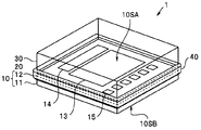
- the imaging device 1 includes an imaging element 10, a cover glass 30 that is a transparent member, and an adhesive layer 20 that bonds the imaging element 10 and the cover glass 30.
- the imaging element 10 includes a semiconductor substrate 11 on which an imaging unit (light receiving unit / pixel unit) 13 is formed and a wiring layer 12. As will be described later, since the side surface of the wiring layer 12 is surrounded by the protection unit 40 having a specific configuration, the imaging device 1 is excellent in moisture resistance.
- drawings are schematic, and the relationship between the thickness and width of each part, the ratio of the thickness of each part, the size of the particles, the content ratio, and the like are different from the actual ones. In some cases, the drawings may include portions having different dimensional relationships and ratios. Furthermore, the shape of the particles in the cross-sectional view is not a cross-sectional shape but a side surface shape, and the size of the particles is greatly different from the actual for convenience of illustration.
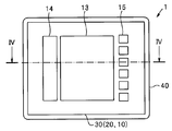
- the imaging unit 13, the circuit unit 14, and the plurality of electrode pads 15 are formed on the first main surface 10SA of the imaging element 10.
- a plurality of junction terminals 18 connected to the respective electrode pads 15 are formed on the second main surface 10SB of the imaging element 10 via the respective through wirings 17.
- the image pickup unit 13 made of a CMOS image pickup device or the like is formed on the main surface of the semiconductor substrate 11 made of silicon or the like by a known semiconductor manufacturing technique.
- the circuit unit 14 includes a semiconductor circuit that processes the signal of the imaging unit 13. Similar to the imaging unit 13, the semiconductor circuit is formed on the main surface of the semiconductor substrate 11 made of silicon or the like by a known semiconductor manufacturing technique.
- the image pickup device 10 including the semiconductor substrate 11 having the wiring layer 12 disposed on the first main surface 10SA is a chip of a wafer level chip size package type, and the image pickup device 10 and the cover glass 30 have the same plan view dimensions. It is. That is, the imaging device 1 is manufactured by cutting and separating a bonded wafer in which an imaging element wafer on which a plurality of imaging elements 10 are formed and a glass wafer are bonded.
- the image sensor 10 is excellent in productivity because it can be mass-produced collectively.
- the imaging device 1 does not necessarily need to be made of a wafer level chip size package type imaging device chip, and may be manufactured by joining the already-divided imaging device 10 and the cover glass 30. Good.
- the at least one insulating layer 12C of the wiring layer 12 is made of a low dielectric constant material (Low-k material).
- the electrode pad 15 is connected to the imaging unit 13 and the circuit unit 14 via the wiring layer 12.
- the conductive materials of the plurality of conductor layers 12A may be made of different materials.
- the insulating material of the plurality of insulating layers 12B may be made of different materials.
- the at least one insulating layer 12C is made of a low dielectric constant material (Low-k material).
- the lower limit of the relative dielectric constant k of the low dielectric constant material is 2.0 or more, preferably 1.5 or more, due to technical limitations.
- the low dielectric constant material of the insulating layer 12C is a porous (porous) carbon-doped silicon oxide film (SiOC).
- Porous SiOC is formed as a porous body having voids due to its structure, and can have a relative dielectric constant k of 2.7.
- a fluorine-doped silicon oxide film SiOF / FSG
- HSQ hydrogen-containing polysiloxane
- MSQ methyl-containing polysiloxane
- organic system polyimide system, parylene system, Fluorine resin-based materials
- the cover glass 30 that is a transparent member bonded to the first main surface 10SA of the image sensor 10 through the adhesive layer 20 has the same planar view size as that of the image sensor 10.
- the transparent member may be made of a resin or the like as long as it has a high transmittance in the wavelength region of light received by the imaging unit 13.
- the cover glass 30 having a sufficiently large thickness blocks moisture from penetrating into the imaging unit 13 and the circuit unit 14.
- the adhesive layer 20 is made of an ultraviolet curable or thermosetting epoxy resin, silicone resin, or the like that has better moisture resistance than the low dielectric constant material of the insulating layer 12C. In the case where the microlens array is disposed immediately above the imaging unit 13, the adhesive layer 20 may not be disposed.
- the imaging device 1 is housed in a shield case 60 to which an objective lens optical system 61 is fixed, and is disposed in the endoscope 2 as an imaging unit 3.
- the junction terminal 18 of the imaging device 1 is electrically connected to the signal cable 63 via the wiring board 64.
- the signal cable 63 is connected to the processor 4 that controls the imaging device and simultaneously processes the imaging signal.
- the gap between the side surface of the image sensor 10 and the inner wall of the shield case 60 is sealed with a sealing resin 62.
- the sealing resin 62 is selected from ultraviolet curable or thermosetting resins having excellent moisture resistance such as epoxy resin or silicone resin.
- the shield case 60 is made of a metal such as stainless steel, has a light shielding function and an electromagnetic noise resistance improvement function, and has moisture resistance to prevent moisture penetration. As will be described later, an imaging unit that does not include the shield case 60 may be used to reduce the diameter of the endoscope 2.
- the side surface of the wiring layer 12 is protected by the sealing resin 62 and the shield case 60.
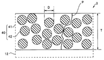
- the image capturing apparatus 1 is provided with a protection unit 40.
- the shielding particles 42 having a moisture permeability lower than that of the resin 41 are dispersed in the resin 41.
- the moisture permeability was evaluated by preparing a test film having a predetermined thickness and JIS Z 0208 (cup method). For example, it can be confirmed that the moisture permeability of the particles is lower than the moisture permeability of the resin 41 by comparing the moisture permeability of the test film made of only the resin 41 and the test film made of the resin 41 in which the particles are dispersed.
- blocking particles 42 made of silica or alumina.
- the thickness T of the protection part 40 is, for example, a value measured from a photograph obtained by photographing a cross section with an electron microscope.
- the particle diameter D is an arithmetic average value measured from a photograph taken with an electron microscope of particles before dispersion.
- the blocking particles 42 fine powder, filler
- the blocking particles 42 are not spherical, but may be oval, rectangular, rod-like, fibrous or amorphous. Further, the diameter D of the particles may have a predetermined distribution.
- the protection part 40 may contain particles having different particle diameters, it is preferable that 90% by weight or more of the particles are within the above range as a proportion of the blocking particles 42.
- the protection unit 40 in which the blocking particles 42 having moisture permeability lower than that of the resin 41 are dispersed can effectively prevent moisture from entering, as shown in FIG. It is estimated to be. If the diameter D of the blocking particles 42 is equal to or greater than the lower limit of the range, a predetermined moisture permeability improving effect is confirmed. If the diameter D is equal to or lower than the upper limit of the range, the dispersibility of the blocking particles 42 in the resin 41 is good. It becomes easy.
- the content of the blocking particles 42 is preferably 30% by weight or more, and particularly preferably 75% by weight or more. However, if the particle content is too high, the adhesive strength to the substrate is lowered, so that it is preferably 95% by weight or less, particularly preferably 90% by weight or less.
- a particle content rate is a preparation value of the dispersion liquid to apply
- the imaging device 1 is a chip size package type semiconductor device having a small size in plan view, and has a high reliability even when the low dielectric constant material (Low-k material) is exposed on the side surface of the wiring layer 12. It has.
- the imaging apparatus 1 did not deteriorate in characteristics even when left in a high-temperature and high-humidity environment of 85 ° C. and 85% humidity for 1000 hours, for example. Further, the performance of the endoscope 2 provided with the imaging device 1 was not impaired even after a predetermined sterilization treatment or the like was performed.
- the protection unit 40 covered the side surface of the wiring layer 12.
- the protective part only needs to cover at least the side surface of the wiring layer 12, in other words, the protective part 40 is not only the side surface of the wiring layer 12, but also the side surface of the cover glass 30, the semiconductor substrate 11, and the adhesive layer 20 thereof. May be covered.
- the protection unit 40A made of the resin 41 including the blocking particles 42 as in the protection unit 40, the imaging device 1A. Not only the side surface of the wiring layer 12 but also the inside of the shield case 60 is sealed.
- the sealing resin 62A has a configuration in which the blocking particles 42 having a moisture permeability lower than the moisture permeability of the resin are dispersed in the resin 41.
- the protection unit 40B of the imaging device 1B of the endoscope 2B according to the second modification of the first embodiment described below covers the side surface of the wiring layer 12 in the same manner as the imaging device 1 of the first embodiment.
- the content rate of the blocking particles 42 is changed in the thickness direction, and the content rate of the inner first protective part 40B1 in contact with the wiring layer 12 is set to the outer side. It is smaller than the particle content of the second protective part 40B2.
- the protection part 40B includes the first protection part 40B1 and the second protection part 40B2 having different particle contents, the adhesive strength to the wiring layer 12 is sufficiently high, and the blocking particles 42 of the protection part 40B The content rate can be increased.
- the side surface of the wiring layer 12 is covered by the first protection unit 40C1, and the first The inside of the shield case 60 is sealed with a sealing resin 62C, which is the second protective part 40C2 having a higher particle content than the protective part 40C1.
- the content rate of the blocking particles 42 is changed as in Modifications 2 and 3
- the content rate of the highest region is preferably 30% by weight or more and 95% by weight or less, particularly preferably. It is 50 weight% or more and 90 weight% or less.
- the content of the lowest region may be 0%.
- the content of the entire protective part is preferably 30% by weight or more.
- the protective part in which the content of the blocking particles 42 is changed in the thickness direction may be a multilayer structure of three or more layers, or a composition gradient film.
- the imaging unit 3C includes the first protective part 40C1 and the second protective part 40C2 having different particle contents, the adhesive strength to the wiring layer 12 is sufficiently high, and the blocking particles 42 in the protective part The content rate can be increased.
- an endoscope 2D of the second embodiment will be described. Since the endoscope 2D is similar to the endoscope 2 according to the first embodiment, the same components are denoted by the same reference numerals and description thereof is omitted.
- the endoscope 2D is different from the endoscope 2 of the first embodiment in the configuration of the protection unit 40D.
- the protection unit 40D of the imaging device 1D of the endoscope 2D includes moisture absorbing particles 43 whose water absorption rate is higher than the water absorption rate of the resin 41 in addition to the blocking particles 42.
- the water absorption rate was evaluated according to JIS 7209. For example, when an epoxy resin or a silicone resin is used as the resin 41, moisture absorbing particles 43 made of carbon black, carbon nanotubes, bentonite, or zeolite are used.
- the hygroscopic particles 43 trap moisture that has entered the resin 41.
- the protection part 40 ⁇ / b> D including the moisture absorption particles 43 in addition to the blocking particles 42 has a higher effect of preventing moisture from entering the wiring layer 12 than the protection part 40.
- the endoscope 2D has the effect of the endoscope 2 and is more reliable.
- the distal end portion 2a of the endoscope 2D is exposed to a high humidity environment only during use.
- moisture may enter during insertion into the body and during sterilization after use.
- the moisture trapped by the hygroscopic particles 43 is released to the outside when not in use, particularly during the drying process.
- the content of the hygroscopic particles 43 is preferably 5% by weight or more at which the effect of improving hygroscopicity becomes remarkable, and the upper limit is 65% by weight. Moreover, it is preferable that the sum total of the content rate of the interruption
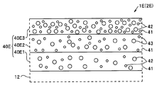
- the protection unit 40E of the imaging device 1E includes a first protection unit 40E1 including blocking particles 42 and a hygroscopic particle 43.
- the three protective portions 40E2 and the third protective portion 40E3 including the blocking particles 42 are stacked in order.
- the particle content rate of the first protection part 40E1 in contact with the wiring layer 12 is smaller than the particle content rate of the outer third protection part 40E3. For this reason, the protective part 40E has strong adhesive strength. Furthermore, when the moisture that has penetrated into the third protection unit 40E3 reaches the protection unit 40E2, it is trapped by the protection unit 40E2. When there is moisture that has passed through the protection unit 40E2 without being trapped, the moisture is blocked by the protection unit 40E1.
- the endoscope 2E has the effect of the endoscope 2D and the like, and is more reliable.
- the first protection unit 40F1 covers the side surface of the wiring layer 12.
- the second protection unit 40F2 covers the first protection unit 40F1
- the third protection unit 40F3 seals the rear end portion of the imaging device as the sealing resin 62F.
- the imaging unit 3F does not include a shield case, and the objective lens optical system 61 is fixed to a frame member 60F joined to the cover glass 30.
- the endoscope 2F has the effect of the endoscope 2E and is more reliable. In addition, the endoscope 2F is easier to reduce in diameter than an endoscope having a shield case.
- Imaging device In the above description, the endoscope in which the side surface of the wiring layer 12 of the imaging apparatus is covered with the protection units 40 and 40A to 40F having a specific configuration has been described. However, it goes without saying that the imaging devices 1, 1 to 1F can be used as various imaging devices used in an environment where high moisture resistance is required.
- the following imaging devices have excellent moisture resistance and high reliability.
- a light receiving portion is formed on the first main surface, a semiconductor substrate having a junction terminal electrically connected to the light receiving portion on the second main surface, and disposed on the first main surface of the semiconductor substrate
- An imaging device comprising: An imaging device having a protection unit, wherein at least a side surface of the wiring layer of the imaging element is covered with a blocking particle having a moisture permeability lower than that of the resin.
Landscapes
- Health & Medical Sciences (AREA)
- Life Sciences & Earth Sciences (AREA)
- Surgery (AREA)
- Physics & Mathematics (AREA)
- Optics & Photonics (AREA)
- Medical Informatics (AREA)
- Animal Behavior & Ethology (AREA)
- Radiology & Medical Imaging (AREA)
- Nuclear Medicine, Radiotherapy & Molecular Imaging (AREA)
- Engineering & Computer Science (AREA)
- Biomedical Technology (AREA)
- Heart & Thoracic Surgery (AREA)
- Biophysics (AREA)
- Molecular Biology (AREA)
- Pathology (AREA)
- General Health & Medical Sciences (AREA)
- Public Health (AREA)
- Veterinary Medicine (AREA)
- Astronomy & Astrophysics (AREA)
- General Physics & Mathematics (AREA)
- Endoscopes (AREA)
- Solid State Image Pick-Up Elements (AREA)
- Instruments For Viewing The Inside Of Hollow Bodies (AREA)
- Studio Devices (AREA)
Abstract
内視鏡2は、第1の主面10SAに撮像部13が形成され第2の主面10SBに接合端子18を有する半導体基板11と、前記半導体基板11の前記第1の主面10SAに配設された、導体層12Aが絶縁層12B、12Cを介して積層されている、配線層12と、を有する撮像素子10と、前記撮像素子10の前記第1の主面側の全体を覆うように接着されているカバーガラス30と、を具備する撮像装置1が、挿入部の先端部2aに配設されている内視鏡2であって、少なくとも前記撮像素子10の前記配線層12の側面を覆う、樹脂41に透湿性が前記樹脂41の透湿性よりも低い遮断粒子42が分散されている、保護部40を有する。
Description
本発明は、配線層に低誘電率材料を有する撮像装置を具備する内視鏡、および前記撮像装置、に関する。
CMOS受光素子等からなる受光部が主面(受光面)に形成された撮像素子を具備するチップサイズパッケージ型の撮像装置は、小径であることから内視鏡に用いられている。半導体技術により作製された微細パターンからなる受光部と、配線板等が接続される大きな接合電極との整合性を取るために、撮像素子には導体層と絶縁層とからなる配線層が不可欠である。近年、撮像装置の高性能化のために、配線層の絶縁層として酸化シリコンよりも低誘電率の材料、いわゆるLow-k材料を用いることが検討されている。
しかし、Low-k材料は、耐湿性/耐水性、すなわち水分(水蒸気等を含む)の浸透に対する耐性において、従来の絶縁層材料よりも劣っている。Low-k材料を絶縁層とするチップサイズパッケージ型の撮像装置は、Low-k材料が外周部に露出しているため、信頼性が十分ではないおそれがあった。すなわち、Low-k材料からなる絶縁層に水が侵入すると、比誘電率が上昇し寄生容量が増加し信号遅延が生じることにより動作不良が生じたり、絶縁層が剥離したりするといった問題が発生しかねないおそれがあった。
日本国特開2011-166080号公報には、撮像素子をシールドケースに収納した撮像装置が開示されている。撮像素子とシールドケースとの隙間には封止樹脂が充填されている。
しかし、上記公報には、封止樹脂を介して浸透した水分による影響については何の開示も示唆もない。これは、撮像素子の絶縁層としてLow-k材料を用いていないためであると推察される。
本発明の実施形態は、耐湿性に優れた信頼性の高い内視鏡、および耐湿性に優れた信頼性の高い撮像装置を提供することを目的とする。
本発明の実施形態の内視鏡は、第1の主面に受光部が形成され、第2の主面に前記受光部と電気的に接続されている接合端子を有する半導体基板と、前記半導体基板の前記第1の主面に配設された、導体層が絶縁層を介して積層されている、配線層と、を有する撮像素子と、前記撮像素子の前記第1の主面側の全体を覆うように接着されているカバーガラスと、を具備する撮像装置が、挿入部の先端部に配設されている内視鏡であって、少なくとも前記撮像素子の前記配線層の側面を覆う、樹脂に透湿性が前記樹脂の透湿性よりも低い遮断粒子が分散されている、保護部を有する。
別の実施形態の撮像装置は、第1の主面に受光部が形成され、第2の主面に前記受光部と電気的に接続されている接合端子を有する半導体基板と、前記半導体基板の前記第1の主面に配設された、導体層が絶縁層を介して積層されている配線層と、を有する撮像素子と、前記撮像素子の前記第1の主面側の全体を覆うように接着されているカバーガラスと、を具備する撮像装置であって、少なくとも前記撮像素子の前記配線層の側面を覆う、樹脂に透湿性が前記樹脂の透湿性よりも低い遮断粒子が分散されている、保護部を有する。
本発明によれば、耐湿性に優れた信頼性の高い内視鏡、および耐湿性に優れた信頼性の高い撮像装置を提供することができる。
<第1実施形態>
図1に示すように、本実施形態の内視鏡2は、プロセッサ4と共に内視鏡システム9を構成している。内視鏡2は、撮像装置1を含む撮像ユニット3が配設された先端部2aと、先端部2aから延設された細長い挿入部2bと、挿入部2bの基端部側に配設された操作部2cと、操作部2cから延設されたユニバーサルコード2dと、ユニバーサルコード2dの基端部側に配設されたコネクタ2eと、を有する。
図1に示すように、本実施形態の内視鏡2は、プロセッサ4と共に内視鏡システム9を構成している。内視鏡2は、撮像装置1を含む撮像ユニット3が配設された先端部2aと、先端部2aから延設された細長い挿入部2bと、挿入部2bの基端部側に配設された操作部2cと、操作部2cから延設されたユニバーサルコード2dと、ユニバーサルコード2dの基端部側に配設されたコネクタ2eと、を有する。
コネクタ2eは、プロセッサ4と着脱自在に接続される。プロセッサ4は、撮像装置1の撮像信号を、信号処理して画像信号をモニタ4Aに出力する。
図2~図4に示すように、撮像装置1は、撮像素子10と、透明部材であるカバーガラス30と、撮像素子10とカバーガラス30とを接着している接着層20と、を具備する。撮像素子10は、撮像部(受光部/画素部)13が形成された半導体基板11と配線層12とを含む。後述するように、配線層12の側面が特定の構成の保護部40により取り囲まれているため、撮像装置1は耐湿性に優れている。
なお、図面は、模式的なものであり、各部分の厚みと幅との関係、夫々の部分の厚みの比率、粒子の大きさ、および含有率等は現実のものとは異なることに留意すべきであり、図面の相互間においても互いの寸法の関係や比率が異なる部分が含まれている場合がある。さらに、断面図における粒子の形状は断面形状ではなく側面形状とし、粒子の大きさも図示の都合上、実際とは大きく異なる。
撮像素子10の第1の主面10SAには、撮像部13と、回路部14と、複数の電極パッド15と、が形成されている。一方、撮像素子10の第2の主面10SBには、それぞれの貫通配線17を介して、それぞれの電極パッド15と接続された複数の接合端子18が形成されている。
CMOS撮像素子等からなる撮像部13は、シリコン等からなる半導体基板11の主面に公知の半導体製造技術により形成されている。
回路部14は撮像部13の信号を処理する半導体回路を含んでいる。半導体回路は撮像部13と同様に、シリコン等からなる半導体基板11の主面に公知の半導体製造技術により形成されている。
配線層12が第1の主面10SAに配設された半導体基板11からなる撮像素子10は、ウエハレベルチップサイズパッケージ型のチップであり、撮像素子10とカバーガラス30とは平面視寸法が同じである。すなわち、複数の撮像素子10が形成された撮像素子ウエハと、ガラスウエハとが接着された接合ウエハを、切断し個片化することにより撮像装置1は製造されている。撮像素子10は一括して大量生産できるため生産性に優れている。
撮像装置1については、むろん、必ずしもウエハレベルチップサイズパッケージ型の撮像素子チップからなる必要はなく、既に個片化された撮像素子10とカバーガラス30とを接合して製造するものであってもよい。
そして、配線層12の少なくとも1つの絶縁層12Cは、低誘電率材料(Low-k材料)からなる。電極パッド15は、配線層12を介して撮像部13や回路部14と接続されている。
なお、複数の導体層12Aの導電性材料は異なる材料で構成されていてもよい。また、複数の絶縁層12Bの絶縁材料は異なる材料で構成されていてもよい。そして、少なくとも1つの絶縁層12Cは、低誘電率材料(Low-k材料)からなる。
低誘電率材料とは、酸化シリコン(k=4.0)よりも比誘電率kが低い材料であり、好ましくは比誘電率kが3.0以下の材料である。低誘電率材料の比誘電率kの下限値は、技術的限界により、2.0以上、好ましくは1.5以上である。
撮像装置1では、絶縁層12Cの低誘電率材料は、多孔質(ポーラス状)の炭素ドープシリコン酸化膜(SiOC)である。ポーラスSiOCは、その構造上、空隙を有している多孔質体として形成され、比誘電率kを2.7とすることも可能である。
絶縁層12Cの材料としては、SiOCの他、フッ素ドープシリコン酸化膜(SiOF/FSG)、水素含有ポリシロキサン(HSQ)系、メチル含有ポリシロキサン(MSQ)系、有機系(ポリイミド系、パリレン系、フッ素樹脂系)材料等も使用可能である。
そして、接着層20を介して撮像素子10の第1の主面10SAに接着されている透明部材であるカバーガラス30は、平面視寸法が撮像素子10と同じである。透明部材は、撮像部13が受光する光の波長領域において透過率が高い材料であれば、樹脂等から構成されていてもよい。厚さが十分に厚いカバーガラス30は、撮像部13および回路部14等への上部からの水分の浸透を遮断している。
接着層20は、絶縁層12Cの低誘電率材料よりも耐湿性に優れた、紫外線硬化型または熱硬化型の、エポキシ樹脂またはシリコーン樹脂等からなる。なお、撮像部13の直上にマイクロレンズアレイが配設されている場合においては、接着層20は配設されていなくともよい。
図5に示すように、撮像装置1は、対物レンズ光学系61が固定されたシールドケース60の内部に収容され、撮像ユニット3として内視鏡2に配設される。撮像装置1の接合端子18は配線板64を介して信号ケーブル63と電気的に接続されている。信号ケーブル63は撮像装置の制御等を行うと同時に撮像信号を処理するプロセッサ4に接続される。
撮像素子10の側面とシールドケース60の内壁との隙間は封止樹脂62により封止されている。封止樹脂62は、紫外線硬化型または熱硬化型の、エポキシ樹脂またはシリコーン樹脂等、の耐湿性に優れた樹脂から選択される。シールドケース60はステンレス等の金属からなり、遮光機能および電磁ノイズ耐性改善機能を有するとともに、水分の浸透を防止する耐湿性を有する。なお、後述するように、内視鏡2の細径化のためには、シールドケース60を具備しない撮像ユニットであってもよい。
以上の説明のように、配線層12の側面は、封止樹脂62およびシールドケース60で保護されている。しかし、配線層12への水分の浸入を更に確実に防止するために、撮像装置1には、保護部40が配設されている。
図6に示すように、保護部40は、樹脂41に、透湿性が樹脂41よりも低い遮断粒子42が分散されている。透湿性は、所定厚さの試験フィルムを作製し、JIS Z 0208(カップ法)にて評価した。例えば、樹脂41のみからなる試験フィルムと、粒子を分散した樹脂41からなる試験フィルムと、の透湿性の比較から、粒子の透湿性が樹脂41の透湿性よりも低いことが確認できる。
例えば、樹脂としてエポキシ樹脂またはシリコーン樹脂を用いた場合には、シリカ、またはアルミナからなる遮断粒子42を用いることが好ましい。
さらに、遮断粒子42の直径Dが保護部40の厚さTの1/100以上1/5以下であると、透湿性が大きく改善する(図7参照)。保護部40の厚さTは、例えば、断面を電子顕微鏡で撮影した写真から計測した値であり凹凸がある場合は算出平均値である。一方、粒子の直径Dは、分散前の粒子を、電子顕微鏡で撮影した写真から計測した算術平均値である。遮断粒子42(微少粉体、フィラー)は、球形ではなく、楕円形、矩形、棒状、繊維状または無定型等であってもよい。また、粒子の直径Dは、所定の分布を有していてもよい。さらに、保護部40は異なる粒径の粒子を含んでいてもよいが、遮断粒子42に占める割合として、90重量%以上の粒子が前記範囲内であることが好ましい。
透湿性が樹脂41よりも低い遮断粒子42が分散されている保護部40が水分の浸入を効果的に防止できるのは、図7に示すように、水分の浸入経路Pが遮断粒子42により長くなるためと推定される。遮断粒子42の直径Dが前記範囲の下限以上であれば、所定の透湿性改善効果が確認され、前記範囲の上限以下であれば、樹脂41における遮断粒子42の分散性が良く、充填等も容易となる。
なお、上記効果をより効果的に得るためには、遮断粒子42の含有率が30重量%以上であることが好ましく、特に好ましくは75重量%以上である。ただし、粒子含有率が高すぎると基体への接着強度が低下するため、95重量%以下が好ましく、特に好ましくは90重量%以下である。なお、粒子含有率は、塗布する分散液の調合値である。
撮像装置1の配線層12は、側面からの水分の浸透が、保護部40、封止樹脂62およびシールドケース60により遮断されている。そのため、撮像装置1は、平面視寸法が小さいチップサイズパッケージ型半導体装置で、配線層12の側面に低誘電率材料(Low-k材料)が露出している構成であっても、高い信頼性を備えている。
撮像装置1は、例えば、85℃、湿度85%の高温多湿環境に1000時間放置しても特性が劣化することがなかった。また、撮像装置1が配設された内視鏡2は、所定の滅菌処理等が施された後も、性能が損なわれることはなかった。
<第1実施形態の変形例>
次に説明する第1実施形態の変形例の内視鏡は、第1実施形態の内視鏡2と類似し、内視鏡2の効果を有しているため、同じ機能の構成要素には同じ符号を付し、説明は省略する。
次に説明する第1実施形態の変形例の内視鏡は、第1実施形態の内視鏡2と類似し、内視鏡2の効果を有しているため、同じ機能の構成要素には同じ符号を付し、説明は省略する。
内視鏡2では、保護部40は配線層12の側面を覆っていた。しかし、保護部は、少なくとも配線層12の側面を覆っていればよい、言い換えれば、保護部40が配線層12の側面だけでなく、カバーガラス30と半導体基板11およびその接着層20の側面等を覆っていてもよい。
例えば、図8に示す、第1実施形態の変形例1の内視鏡2Aの撮像ユニット3Aでは、保護部40と同じように遮断粒子42を含む樹脂41からなる保護部40Aにより、撮像装置1Aの配線層12の側面だけでなく、シールドケース60の内部が封止されている。言い換えれば、封止樹脂62Aが、樹脂41に、透湿性が樹脂の透湿性よりも低い遮断粒子42が分散されている構成である。
次に説明する第1実施形態の変形例2の内視鏡2Bの撮像装置1Bの保護部40Bは、第1実施形態の撮像装置1と同じように、配線層12の側面を覆っている。
しかし、図9に示すように、保護部40Bは遮断粒子42の含有率が厚さ方向で変化しており、配線層12と接する内側の第1の保護部40B1の粒子含有率が、外側の第2の保護部40B2の粒子含有率よりも小さい。
保護部40Bは、粒子含有率が異なる第1の保護部40B1と第2の保護部40B2とからなるため、配線層12への接着強度が十分に高く、かつ、保護部40Bの遮断粒子42の含有率を大きくできる。
さらに、図10に示す第1実施形態の変形例3の内視鏡2Cの撮像装置1Cを含む撮像ユニット3Cでは、第1の保護部40C1により配線層12の側面が覆われており、第1の保護部40C1よりも粒子含有率の高い第2の保護部40C2である封止樹脂62Cによりシールドケース60の内部が封止されている。
なお、変形例2、3のように、遮断粒子42の含有率が変化している場合には、最も高い領域の含有率が30重量%以上95重量%以下であることが好ましく、特に好ましくは50重量%以上90重量%以下である。一方、最も低い領域の含有率は0%でもよい。ただし、保護部全体の含有率は30重量%以上であることが好ましい。
なお、厚さ方向で遮断粒子42の含有率が変化している保護部は、3層以上の多層構造でもよいし、組成傾斜膜でもよい。
撮像ユニット3Cは、粒子含有率が異なる第1の保護部40C1と第2の保護部40C2とからなるため、配線層12への接着強度が十分に高く、かつ、保護部中の遮断粒子42の含有率を大きくできる。
<第2実施形態>
次に第2実施形態の内視鏡2Dについて説明する。内視鏡2Dは、第1実施形態の内視鏡2と、類似しているため、同じ構成要素には同じ符号を付し説明は省略する。
次に第2実施形態の内視鏡2Dについて説明する。内視鏡2Dは、第1実施形態の内視鏡2と、類似しているため、同じ構成要素には同じ符号を付し説明は省略する。
内視鏡2Dは、第1実施形態の内視鏡2とは、保護部40Dの構成が異なる。
図11に示すように、内視鏡2Dの撮像装置1Dの保護部40Dは、遮断粒子42に加えて、吸水率が樹脂41の吸水率よりも高い吸湿粒子43を含む。
吸水率は、JIS 7209にて評価した。例えば、樹脂41としてエポキシ樹脂またはシリコーン樹脂を用いた場合には、カーボンブラック、カーボンナノチューブ、ベントナイト、またはゼオライトからなる吸湿粒子43を用いる。
吸湿粒子43は、樹脂41に浸入した水分をトラップする。このため、遮断粒子42に加えて吸湿粒子43を含む保護部40Dは、保護部40よりも配線層12への水分の浸入防止効果が高い。このため、内視鏡2Dは内視鏡2の効果を有し、さらに信頼性が高い。
すなわち、内視鏡2Dの先端部2aは、使用時等にだけ高湿度環境にさらされる。例えば医療用内視鏡であれば、体内に挿入される間および使用後の滅菌処理の間に、水分が浸入する可能性がある。吸湿粒子43がトラップした水分は、使用していない時、特に乾燥処理時に外部へ放出される。
吸湿粒子43の含有率は、吸湿性改善効果が顕著となる5重量%以上であることが好ましく、上限は65重量%である。また、遮断粒子42の含有率と吸湿粒子43の含有率との合計が30重量%以上95重量%以下であることが好ましい。
なお、遮光性を有する、例えばカーボンブラックを吸湿粒子43として用いることにより、撮像素子への外光の入射を防止することができる。
<第2実施形態の変形例>
第2実施形態の変形例1の内視鏡2Eでは、図12に示すように、撮像装置1Eの保護部40Eが、遮断粒子42を含む第1の保護部40E1と、吸湿粒子43を含む第2の保護部40E2と、遮断粒子42を含む第3の保護部40E3と、が順に積層された3層構造である。
第2実施形態の変形例1の内視鏡2Eでは、図12に示すように、撮像装置1Eの保護部40Eが、遮断粒子42を含む第1の保護部40E1と、吸湿粒子43を含む第2の保護部40E2と、遮断粒子42を含む第3の保護部40E3と、が順に積層された3層構造である。
そして、配線層12と接する第1の保護部40E1の粒子含有率が、外側の第3の保護部40E3の粒子含有率よりも少ない。このため、保護部40Eは接着強度が強い。さらに、第3の保護部40E3に浸透した水分が保護部40E2へ至ったとき、保護部40E2でトラップされる。そして、トラップされきらずに保護部40E2を通過した水分があった場合、その水分は保護部40E1で遮断される。
内視鏡2Eは、内視鏡2D等の効果を有し、さらに信頼性が高い。
次に、図13に示す第2実施形態の変形例2の内視鏡2Fでは、撮像ユニット3Fの撮像装置1Fの保護部40Fでは、配線層12の側面を第1の保護部40F1が覆っており、さらに、第2の保護部40F2が第1の保護部40F1を覆っており、さらに第3の保護部40F3が封止樹脂62Fとして、撮像装置の後端部を封止している。
なお、撮像ユニット3Fはシールドケースを具備しておらず、対物レンズ光学系61は、カバーガラス30と接合された枠部材60Fに固定されている。
内視鏡2Fは、内視鏡2Eの効果を有し、さらに信頼性が高い。また、内視鏡2Fは、シールドケースを具備する内視鏡よりも細径化が容易である。
<撮像装置>
なお、以上の説明では、撮像装置の配線層12の側面を特定構成の保護部40、40A~40Fが覆っている内視鏡について説明した。しかし、高い防湿性が要求される環境で使用される各種の撮像装置として、撮像装置1、1~1Fを用いることができることは言うまでもない。
なお、以上の説明では、撮像装置の配線層12の側面を特定構成の保護部40、40A~40Fが覆っている内視鏡について説明した。しかし、高い防湿性が要求される環境で使用される各種の撮像装置として、撮像装置1、1~1Fを用いることができることは言うまでもない。
例えば、以下の撮像装置は、耐湿性に優れており、信頼性が高い。
第1の主面に受光部が形成され、第2の主面に前記受光部と電気的に接続されている接合端子を有する半導体基板と、前記半導体基板の前記第1の主面に配設された、導体層が絶縁層を介して積層されている配線層と、を有する撮像素子と、前記撮像素子の前記第1の主面側の全体を覆うように接着されているカバーガラスと、を具備する撮像装置であって、
少なくとも前記撮像素子の前記配線層の側面を覆う、樹脂に透湿性が前記樹脂の透湿性よりも低い遮断粒子が分散されている、保護部を有する撮像装置。
少なくとも前記撮像素子の前記配線層の側面を覆う、樹脂に透湿性が前記樹脂の透湿性よりも低い遮断粒子が分散されている、保護部を有する撮像装置。
以上のように本発明は上述した実施形態等に限定されるものではなく、本発明の要旨を変えない範囲において、種々の変更、改変等ができる。
1、1A~1F…撮像装置
2、2A~2F…内視鏡
3…撮像ユニット
9…内視鏡システム
10…撮像素子
11…半導体基板
12…配線層
13…撮像部
14…回路部
15…電極パッド
17…貫通配線
18…接合端子
20…接着層
30…カバーガラス
40…保護部
41…樹脂
42…遮断粒子
43…吸湿粒子
50…封止樹脂
60…シールドケース
62…封止樹脂
2、2A~2F…内視鏡
3…撮像ユニット
9…内視鏡システム
10…撮像素子
11…半導体基板
12…配線層
13…撮像部
14…回路部
15…電極パッド
17…貫通配線
18…接合端子
20…接着層
30…カバーガラス
40…保護部
41…樹脂
42…遮断粒子
43…吸湿粒子
50…封止樹脂
60…シールドケース
62…封止樹脂
Claims (12)
- 第1の主面に受光部が形成され、第2の主面に前記受光部と電気的に接続されている接合端子を有する半導体基板と、前記半導体基板の前記第1の主面に配設された、導体層が絶縁層を介して積層されている、配線層と、を有する撮像素子と、
前記撮像素子の前記第1の主面側の全体を覆うように接着されているカバーガラスと、を具備する撮像装置が、挿入部の先端部に配設されている内視鏡であって、
少なくとも前記撮像素子の前記配線層の側面を覆う、樹脂に透湿性が前記樹脂の透湿性よりも低い遮断粒子が分散されている、保護部を有することを特徴とする内視鏡。 - 前記遮断粒子が、シリカ、またはアルミナからなることを特徴とする請求項1に記載の内視鏡。
- 前記遮断粒子の直径が、前記保護部の厚さの1/100以上1/5以下であることを特徴とする請求項1または請求項2に記載の内視鏡。
- 前記遮断粒子の含有率が30重量%以上95重量%以下であることを特徴とする請求項1から請求項3のいずれか1項に記載の内視鏡。
- 前記遮断粒子の含有率が、前記保護部の厚さ方向で変化しており、
外側の領域の粒子含有率が、内側の領域の粒子含有率よりも、大きいことを特徴とする請求項1から請求項4のいずれか1項に記載の内視鏡。 - 前記保護部が、吸水率が前記樹脂の吸水率よりも高い吸湿粒子を含むことを特徴とする請求項1から請求項5のいずれか1項に記載の内視鏡。
- 前記吸湿粒子が、カーボンブラック、カーボンナノチューブ、ベントナイト、または、ゼオライトからなることを特徴とする請求項6に記載の内視鏡。
- 前記吸湿粒子が、遮光性を有することを特徴とする請求項6または請求項7に記載の内視鏡。
- 前記吸湿粒子の含有率が5重量%以上65重量%以下であり、
前記遮断粒子の含有率と前記吸湿粒子の含有率との合計が30重量%以上95重量%以下であることを特徴とする請求項6から請求項8のいずれか1項に記載の内視鏡。 - 前記遮断粒子の含有率および前記吸湿粒子の含有率が、前記保護部の厚さ方向で変化していることを特徴とする請求項6から請求項9のいずれか1項に記載の内視鏡。
- 前記保護部が、前記遮断粒子を含む第1の保護部と、前記吸湿粒子を含む第2の保護部と、前記遮断粒子を含み、粒子含有率が前記第1の保護部よりも大きい、第3の保護部と、が順に積層された多層構造であることを特徴とする請求項10に記載の内視鏡。
- 第1の主面に受光部が形成され、第2の主面に前記受光部と電気的に接続されている接合端子を有する半導体基板と、前記半導体基板の前記第1の主面に配設された、導体層が絶縁層を介して積層されている配線層と、を有する撮像素子と、
前記撮像素子の前記第1の主面側の全体を覆うように接着されているカバーガラスと、を具備する撮像装置であって、
少なくとも前記撮像素子の前記配線層の側面を覆う、樹脂に透湿性が前記樹脂の透湿性よりも低い遮断粒子が分散されている、保護部を有することを特徴とする撮像装置。
Priority Applications (5)
| Application Number | Priority Date | Filing Date | Title |
|---|---|---|---|
| PCT/JP2015/050972 WO2016113885A1 (ja) | 2015-01-15 | 2015-01-15 | 内視鏡および撮像装置 |
| JP2016569181A JPWO2016113885A1 (ja) | 2015-01-15 | 2015-01-15 | 内視鏡および撮像装置 |
| CN201580073455.9A CN107205625B (zh) | 2015-01-15 | 2015-01-15 | 内窥镜和摄像装置 |
| EP15877837.3A EP3245934A4 (en) | 2015-01-15 | 2015-01-15 | Endoscope and imaging device |
| US15/650,267 US20170311785A1 (en) | 2015-01-15 | 2017-07-14 | Endoscope and image pickup apparatus |
Applications Claiming Priority (1)
| Application Number | Priority Date | Filing Date | Title |
|---|---|---|---|
| PCT/JP2015/050972 WO2016113885A1 (ja) | 2015-01-15 | 2015-01-15 | 内視鏡および撮像装置 |
Related Child Applications (1)
| Application Number | Title | Priority Date | Filing Date |
|---|---|---|---|
| US15/650,267 Continuation US20170311785A1 (en) | 2015-01-15 | 2017-07-14 | Endoscope and image pickup apparatus |
Publications (1)
| Publication Number | Publication Date |
|---|---|
| WO2016113885A1 true WO2016113885A1 (ja) | 2016-07-21 |
Family
ID=56405446
Family Applications (1)
| Application Number | Title | Priority Date | Filing Date |
|---|---|---|---|
| PCT/JP2015/050972 Ceased WO2016113885A1 (ja) | 2015-01-15 | 2015-01-15 | 内視鏡および撮像装置 |
Country Status (5)
| Country | Link |
|---|---|
| US (1) | US20170311785A1 (ja) |
| EP (1) | EP3245934A4 (ja) |
| JP (1) | JPWO2016113885A1 (ja) |
| CN (1) | CN107205625B (ja) |
| WO (1) | WO2016113885A1 (ja) |
Families Citing this family (2)
| Publication number | Priority date | Publication date | Assignee | Title |
|---|---|---|---|---|
| JP6956567B2 (ja) * | 2017-08-30 | 2021-11-02 | Hoya株式会社 | 内視鏡 |
| WO2019171460A1 (ja) * | 2018-03-06 | 2019-09-12 | オリンパス株式会社 | 内視鏡用撮像装置、内視鏡、および内視鏡用撮像装置の製造方法 |
Citations (4)
| Publication number | Priority date | Publication date | Assignee | Title |
|---|---|---|---|---|
| JPH11315249A (ja) * | 1998-05-07 | 1999-11-16 | Nippon Steel Chem Co Ltd | コーティング用樹脂組成物及びカラーフィルタ |
| JP2004179245A (ja) * | 2002-11-25 | 2004-06-24 | Toda Kogyo Corp | 半導体封止材料用黒色複合粒子粉末及び半導体封止材料 |
| WO2014045633A1 (ja) * | 2012-09-24 | 2014-03-27 | オリンパス株式会社 | 撮像装置、該撮像装置を備える内視鏡 |
| WO2014174994A1 (ja) * | 2013-04-26 | 2014-10-30 | オリンパス株式会社 | 撮像装置 |
Family Cites Families (13)
| Publication number | Priority date | Publication date | Assignee | Title |
|---|---|---|---|---|
| CN1436819A (zh) * | 2002-02-07 | 2003-08-20 | 户田工业株式会社 | 半导体密封材料用黑色复合颗粒和半导体密封材料 |
| EP1787576A1 (en) * | 2004-08-03 | 2007-05-23 | Olympus Corporation | Resin composition for medical equipment sealing and medical equipment for endoscope having been sealed therewith |
| JP2008159310A (ja) * | 2006-12-21 | 2008-07-10 | Nippon Kasei Chem Co Ltd | ランプ |
| JP5448021B2 (ja) * | 2007-06-29 | 2014-03-19 | 株式会社セガ | レーシングゲーム装置のプログラム、そのプログラムを格納した記録媒体、及びレーシングゲーム装置 |
| JP2010040672A (ja) * | 2008-08-01 | 2010-02-18 | Oki Semiconductor Co Ltd | 半導体装置およびその製造方法 |
| JP5452273B2 (ja) * | 2010-02-15 | 2014-03-26 | オリンパス株式会社 | 半導体装置 |
| JP2011200399A (ja) * | 2010-03-25 | 2011-10-13 | Fujifilm Corp | 内視鏡 |
| WO2013061990A1 (ja) * | 2011-10-24 | 2013-05-02 | 旭硝子株式会社 | 光学フィルタとその製造方法、並びに撮像装置 |
| JPWO2013179764A1 (ja) * | 2012-05-30 | 2016-01-18 | オリンパス株式会社 | 撮像装置の製造方法および半導体装置の製造方法 |
| WO2013187303A1 (ja) * | 2012-06-12 | 2013-12-19 | 三菱瓦斯化学株式会社 | 樹脂組成物、プリプレグ、金属箔張積層板及びプリント配線板 |
| JP2014158563A (ja) * | 2013-02-19 | 2014-09-04 | Olympus Corp | 内視鏡、撮像装置、及び撮像装置の製造方法 |
| JP6110734B2 (ja) * | 2013-06-06 | 2017-04-05 | ルネサスエレクトロニクス株式会社 | 半導体装置 |
| US10085352B2 (en) * | 2014-10-01 | 2018-09-25 | Qorvo Us, Inc. | Method for manufacturing an integrated circuit package |
-
2015
- 2015-01-15 EP EP15877837.3A patent/EP3245934A4/en not_active Withdrawn
- 2015-01-15 CN CN201580073455.9A patent/CN107205625B/zh active Active
- 2015-01-15 JP JP2016569181A patent/JPWO2016113885A1/ja active Pending
- 2015-01-15 WO PCT/JP2015/050972 patent/WO2016113885A1/ja not_active Ceased
-
2017
- 2017-07-14 US US15/650,267 patent/US20170311785A1/en not_active Abandoned
Patent Citations (4)
| Publication number | Priority date | Publication date | Assignee | Title |
|---|---|---|---|---|
| JPH11315249A (ja) * | 1998-05-07 | 1999-11-16 | Nippon Steel Chem Co Ltd | コーティング用樹脂組成物及びカラーフィルタ |
| JP2004179245A (ja) * | 2002-11-25 | 2004-06-24 | Toda Kogyo Corp | 半導体封止材料用黒色複合粒子粉末及び半導体封止材料 |
| WO2014045633A1 (ja) * | 2012-09-24 | 2014-03-27 | オリンパス株式会社 | 撮像装置、該撮像装置を備える内視鏡 |
| WO2014174994A1 (ja) * | 2013-04-26 | 2014-10-30 | オリンパス株式会社 | 撮像装置 |
Non-Patent Citations (1)
| Title |
|---|
| See also references of EP3245934A4 * |
Also Published As
| Publication number | Publication date |
|---|---|
| EP3245934A4 (en) | 2018-08-01 |
| EP3245934A1 (en) | 2017-11-22 |
| US20170311785A1 (en) | 2017-11-02 |
| JPWO2016113885A1 (ja) | 2017-10-19 |
| CN107205625B (zh) | 2019-08-16 |
| CN107205625A (zh) | 2017-09-26 |
Similar Documents
| Publication | Publication Date | Title |
|---|---|---|
| CN105144385B (zh) | 摄像装置 | |
| US11062990B2 (en) | Semiconductor package of using insulating frame | |
| JP5450295B2 (ja) | 撮像装置および撮像装置の製造方法 | |
| KR102887553B1 (ko) | 패시브 디바이스 조립체가 포함된 통합 디바이스 패키지 | |
| CN101866897A (zh) | 具有贯通电极的固体摄像器件 | |
| US9820637B2 (en) | Image pickup apparatus and endoscope including image pickup apparatus | |
| US10930696B2 (en) | Image pickup unit, endoscope, and method for manufacturing image pickup unit | |
| US20110049707A1 (en) | Semiconductor device and method of manufacturing the semiconductor device | |
| JP7491923B2 (ja) | シールドされた一体型デバイスパッケージ | |
| WO2016113885A1 (ja) | 内視鏡および撮像装置 | |
| CN107611147B (zh) | 多芯片塑胶球状数组封装结构 | |
| JP6612264B2 (ja) | 撮像装置および内視鏡 | |
| US20180061779A1 (en) | Semiconductor device | |
| JP2014216554A (ja) | 撮像装置 | |
| JP6270336B2 (ja) | 撮像装置 | |
| JP6412169B2 (ja) | 撮像装置および内視鏡 | |
| WO2018092242A1 (ja) | 素子接合体、撮像モジュール、内視鏡、および素子接合体の製造方法 | |
| CN102339767A (zh) | 半导体元件及其制造方法 |
Legal Events
| Date | Code | Title | Description |
|---|---|---|---|
| 121 | Ep: the epo has been informed by wipo that ep was designated in this application |
Ref document number: 15877837 Country of ref document: EP Kind code of ref document: A1 |
|
| ENP | Entry into the national phase |
Ref document number: 2016569181 Country of ref document: JP Kind code of ref document: A |
|
| REEP | Request for entry into the european phase |
Ref document number: 2015877837 Country of ref document: EP |
|
| NENP | Non-entry into the national phase |
Ref country code: DE |