WO2016129235A1 - 方向性電磁鋼板の製造方法 - Google Patents
方向性電磁鋼板の製造方法 Download PDFInfo
- Publication number
- WO2016129235A1 WO2016129235A1 PCT/JP2016/000505 JP2016000505W WO2016129235A1 WO 2016129235 A1 WO2016129235 A1 WO 2016129235A1 JP 2016000505 W JP2016000505 W JP 2016000505W WO 2016129235 A1 WO2016129235 A1 WO 2016129235A1
- Authority
- WO
- WIPO (PCT)
- Prior art keywords
- steel sheet
- resist
- grain
- mask
- oriented electrical
- Prior art date
- Legal status (The legal status is an assumption and is not a legal conclusion. Google has not performed a legal analysis and makes no representation as to the accuracy of the status listed.)
- Ceased
Links
Images


Classifications
-
- C—CHEMISTRY; METALLURGY
- C25—ELECTROLYTIC OR ELECTROPHORETIC PROCESSES; APPARATUS THEREFOR
- C25F—PROCESSES FOR THE ELECTROLYTIC REMOVAL OF MATERIALS FROM OBJECTS; APPARATUS THEREFOR
- C25F3/00—Electrolytic etching or polishing
- C25F3/02—Etching
- C25F3/06—Etching of iron or steel
-
- C—CHEMISTRY; METALLURGY
- C21—METALLURGY OF IRON
- C21D—MODIFYING THE PHYSICAL STRUCTURE OF FERROUS METALS; GENERAL DEVICES FOR HEAT TREATMENT OF FERROUS OR NON-FERROUS METALS OR ALLOYS; MAKING METAL MALLEABLE, e.g. BY DECARBURISATION OR TEMPERING
- C21D8/00—Modifying the physical properties of ferrous metals or ferrous alloys by deformation combined with, or followed by, heat treatment
- C21D8/12—Modifying the physical properties of ferrous metals or ferrous alloys by deformation combined with, or followed by, heat treatment during manufacturing of articles with special electromagnetic properties
- C21D8/1294—Modifying the physical properties of ferrous metals or ferrous alloys by deformation combined with, or followed by, heat treatment during manufacturing of articles with special electromagnetic properties involving a localised treatment
-
- C—CHEMISTRY; METALLURGY
- C21—METALLURGY OF IRON
- C21D—MODIFYING THE PHYSICAL STRUCTURE OF FERROUS METALS; GENERAL DEVICES FOR HEAT TREATMENT OF FERROUS OR NON-FERROUS METALS OR ALLOYS; MAKING METAL MALLEABLE, e.g. BY DECARBURISATION OR TEMPERING
- C21D6/00—Heat treatment of ferrous alloys
- C21D6/005—Heat treatment of ferrous alloys containing Mn
-
- C—CHEMISTRY; METALLURGY
- C21—METALLURGY OF IRON
- C21D—MODIFYING THE PHYSICAL STRUCTURE OF FERROUS METALS; GENERAL DEVICES FOR HEAT TREATMENT OF FERROUS OR NON-FERROUS METALS OR ALLOYS; MAKING METAL MALLEABLE, e.g. BY DECARBURISATION OR TEMPERING
- C21D6/00—Heat treatment of ferrous alloys
- C21D6/008—Heat treatment of ferrous alloys containing Si
-
- C—CHEMISTRY; METALLURGY
- C21—METALLURGY OF IRON
- C21D—MODIFYING THE PHYSICAL STRUCTURE OF FERROUS METALS; GENERAL DEVICES FOR HEAT TREATMENT OF FERROUS OR NON-FERROUS METALS OR ALLOYS; MAKING METAL MALLEABLE, e.g. BY DECARBURISATION OR TEMPERING
- C21D8/00—Modifying the physical properties of ferrous metals or ferrous alloys by deformation combined with, or followed by, heat treatment
-
- C—CHEMISTRY; METALLURGY
- C21—METALLURGY OF IRON
- C21D—MODIFYING THE PHYSICAL STRUCTURE OF FERROUS METALS; GENERAL DEVICES FOR HEAT TREATMENT OF FERROUS OR NON-FERROUS METALS OR ALLOYS; MAKING METAL MALLEABLE, e.g. BY DECARBURISATION OR TEMPERING
- C21D8/00—Modifying the physical properties of ferrous metals or ferrous alloys by deformation combined with, or followed by, heat treatment
- C21D8/12—Modifying the physical properties of ferrous metals or ferrous alloys by deformation combined with, or followed by, heat treatment during manufacturing of articles with special electromagnetic properties
-
- C—CHEMISTRY; METALLURGY
- C21—METALLURGY OF IRON
- C21D—MODIFYING THE PHYSICAL STRUCTURE OF FERROUS METALS; GENERAL DEVICES FOR HEAT TREATMENT OF FERROUS OR NON-FERROUS METALS OR ALLOYS; MAKING METAL MALLEABLE, e.g. BY DECARBURISATION OR TEMPERING
- C21D8/00—Modifying the physical properties of ferrous metals or ferrous alloys by deformation combined with, or followed by, heat treatment
- C21D8/12—Modifying the physical properties of ferrous metals or ferrous alloys by deformation combined with, or followed by, heat treatment during manufacturing of articles with special electromagnetic properties
- C21D8/1216—Modifying the physical properties of ferrous metals or ferrous alloys by deformation combined with, or followed by, heat treatment during manufacturing of articles with special electromagnetic properties characterised by the working steps
- C21D8/1222—Hot rolling
-
- C—CHEMISTRY; METALLURGY
- C21—METALLURGY OF IRON
- C21D—MODIFYING THE PHYSICAL STRUCTURE OF FERROUS METALS; GENERAL DEVICES FOR HEAT TREATMENT OF FERROUS OR NON-FERROUS METALS OR ALLOYS; MAKING METAL MALLEABLE, e.g. BY DECARBURISATION OR TEMPERING
- C21D8/00—Modifying the physical properties of ferrous metals or ferrous alloys by deformation combined with, or followed by, heat treatment
- C21D8/12—Modifying the physical properties of ferrous metals or ferrous alloys by deformation combined with, or followed by, heat treatment during manufacturing of articles with special electromagnetic properties
- C21D8/1216—Modifying the physical properties of ferrous metals or ferrous alloys by deformation combined with, or followed by, heat treatment during manufacturing of articles with special electromagnetic properties characterised by the working steps
- C21D8/1233—Cold rolling
-
- C—CHEMISTRY; METALLURGY
- C21—METALLURGY OF IRON
- C21D—MODIFYING THE PHYSICAL STRUCTURE OF FERROUS METALS; GENERAL DEVICES FOR HEAT TREATMENT OF FERROUS OR NON-FERROUS METALS OR ALLOYS; MAKING METAL MALLEABLE, e.g. BY DECARBURISATION OR TEMPERING
- C21D8/00—Modifying the physical properties of ferrous metals or ferrous alloys by deformation combined with, or followed by, heat treatment
- C21D8/12—Modifying the physical properties of ferrous metals or ferrous alloys by deformation combined with, or followed by, heat treatment during manufacturing of articles with special electromagnetic properties
- C21D8/1244—Modifying the physical properties of ferrous metals or ferrous alloys by deformation combined with, or followed by, heat treatment during manufacturing of articles with special electromagnetic properties characterised by the heat treatment
- C21D8/1266—Modifying the physical properties of ferrous metals or ferrous alloys by deformation combined with, or followed by, heat treatment during manufacturing of articles with special electromagnetic properties characterised by the heat treatment between cold rolling steps
-
- C—CHEMISTRY; METALLURGY
- C21—METALLURGY OF IRON
- C21D—MODIFYING THE PHYSICAL STRUCTURE OF FERROUS METALS; GENERAL DEVICES FOR HEAT TREATMENT OF FERROUS OR NON-FERROUS METALS OR ALLOYS; MAKING METAL MALLEABLE, e.g. BY DECARBURISATION OR TEMPERING
- C21D8/00—Modifying the physical properties of ferrous metals or ferrous alloys by deformation combined with, or followed by, heat treatment
- C21D8/12—Modifying the physical properties of ferrous metals or ferrous alloys by deformation combined with, or followed by, heat treatment during manufacturing of articles with special electromagnetic properties
- C21D8/1244—Modifying the physical properties of ferrous metals or ferrous alloys by deformation combined with, or followed by, heat treatment during manufacturing of articles with special electromagnetic properties characterised by the heat treatment
- C21D8/1272—Final recrystallisation annealing
-
- C—CHEMISTRY; METALLURGY
- C21—METALLURGY OF IRON
- C21D—MODIFYING THE PHYSICAL STRUCTURE OF FERROUS METALS; GENERAL DEVICES FOR HEAT TREATMENT OF FERROUS OR NON-FERROUS METALS OR ALLOYS; MAKING METAL MALLEABLE, e.g. BY DECARBURISATION OR TEMPERING
- C21D8/00—Modifying the physical properties of ferrous metals or ferrous alloys by deformation combined with, or followed by, heat treatment
- C21D8/12—Modifying the physical properties of ferrous metals or ferrous alloys by deformation combined with, or followed by, heat treatment during manufacturing of articles with special electromagnetic properties
- C21D8/1277—Modifying the physical properties of ferrous metals or ferrous alloys by deformation combined with, or followed by, heat treatment during manufacturing of articles with special electromagnetic properties involving a particular surface treatment
-
- C—CHEMISTRY; METALLURGY
- C21—METALLURGY OF IRON
- C21D—MODIFYING THE PHYSICAL STRUCTURE OF FERROUS METALS; GENERAL DEVICES FOR HEAT TREATMENT OF FERROUS OR NON-FERROUS METALS OR ALLOYS; MAKING METAL MALLEABLE, e.g. BY DECARBURISATION OR TEMPERING
- C21D9/00—Heat treatment, e.g. annealing, hardening, quenching or tempering, adapted for particular articles; Furnaces therefor
- C21D9/46—Heat treatment, e.g. annealing, hardening, quenching or tempering, adapted for particular articles; Furnaces therefor for sheet metals
-
- C—CHEMISTRY; METALLURGY
- C22—METALLURGY; FERROUS OR NON-FERROUS ALLOYS; TREATMENT OF ALLOYS OR NON-FERROUS METALS
- C22C—ALLOYS
- C22C38/00—Ferrous alloys, e.g. steel alloys
- C22C38/001—Ferrous alloys, e.g. steel alloys containing N
-
- C—CHEMISTRY; METALLURGY
- C22—METALLURGY; FERROUS OR NON-FERROUS ALLOYS; TREATMENT OF ALLOYS OR NON-FERROUS METALS
- C22C—ALLOYS
- C22C38/00—Ferrous alloys, e.g. steel alloys
- C22C38/004—Very low carbon steels, i.e. having a carbon content of less than 0,01%
-
- C—CHEMISTRY; METALLURGY
- C22—METALLURGY; FERROUS OR NON-FERROUS ALLOYS; TREATMENT OF ALLOYS OR NON-FERROUS METALS
- C22C—ALLOYS
- C22C38/00—Ferrous alloys, e.g. steel alloys
- C22C38/02—Ferrous alloys, e.g. steel alloys containing silicon
-
- C—CHEMISTRY; METALLURGY
- C22—METALLURGY; FERROUS OR NON-FERROUS ALLOYS; TREATMENT OF ALLOYS OR NON-FERROUS METALS
- C22C—ALLOYS
- C22C38/00—Ferrous alloys, e.g. steel alloys
- C22C38/04—Ferrous alloys, e.g. steel alloys containing manganese
-
- C—CHEMISTRY; METALLURGY
- C22—METALLURGY; FERROUS OR NON-FERROUS ALLOYS; TREATMENT OF ALLOYS OR NON-FERROUS METALS
- C22C—ALLOYS
- C22C38/00—Ferrous alloys, e.g. steel alloys
- C22C38/06—Ferrous alloys, e.g. steel alloys containing aluminium
-
- C—CHEMISTRY; METALLURGY
- C25—ELECTROLYTIC OR ELECTROPHORETIC PROCESSES; APPARATUS THEREFOR
- C25F—PROCESSES FOR THE ELECTROLYTIC REMOVAL OF MATERIALS FROM OBJECTS; APPARATUS THEREFOR
- C25F3/00—Electrolytic etching or polishing
- C25F3/02—Etching
- C25F3/14—Etching locally
-
- G—PHYSICS
- G03—PHOTOGRAPHY; CINEMATOGRAPHY; ANALOGOUS TECHNIQUES USING WAVES OTHER THAN OPTICAL WAVES; ELECTROGRAPHY; HOLOGRAPHY
- G03F—PHOTOMECHANICAL PRODUCTION OF TEXTURED OR PATTERNED SURFACES, e.g. FOR PRINTING, FOR PROCESSING OF SEMICONDUCTOR DEVICES; MATERIALS THEREFOR; ORIGINALS THEREFOR; APPARATUS SPECIALLY ADAPTED THEREFOR
- G03F7/00—Photomechanical, e.g. photolithographic, production of textured or patterned surfaces, e.g. printing surfaces; Materials therefor, e.g. comprising photoresists; Apparatus specially adapted therefor
- G03F7/004—Photosensitive materials
- G03F7/022—Quinonediazides
-
- G—PHYSICS
- G03—PHOTOGRAPHY; CINEMATOGRAPHY; ANALOGOUS TECHNIQUES USING WAVES OTHER THAN OPTICAL WAVES; ELECTROGRAPHY; HOLOGRAPHY
- G03F—PHOTOMECHANICAL PRODUCTION OF TEXTURED OR PATTERNED SURFACES, e.g. FOR PRINTING, FOR PROCESSING OF SEMICONDUCTOR DEVICES; MATERIALS THEREFOR; ORIGINALS THEREFOR; APPARATUS SPECIALLY ADAPTED THEREFOR
- G03F7/00—Photomechanical, e.g. photolithographic, production of textured or patterned surfaces, e.g. printing surfaces; Materials therefor, e.g. comprising photoresists; Apparatus specially adapted therefor
- G03F7/004—Photosensitive materials
- G03F7/022—Quinonediazides
- G03F7/023—Macromolecular quinonediazides; Macromolecular additives, e.g. binders
-
- G—PHYSICS
- G03—PHOTOGRAPHY; CINEMATOGRAPHY; ANALOGOUS TECHNIQUES USING WAVES OTHER THAN OPTICAL WAVES; ELECTROGRAPHY; HOLOGRAPHY
- G03F—PHOTOMECHANICAL PRODUCTION OF TEXTURED OR PATTERNED SURFACES, e.g. FOR PRINTING, FOR PROCESSING OF SEMICONDUCTOR DEVICES; MATERIALS THEREFOR; ORIGINALS THEREFOR; APPARATUS SPECIALLY ADAPTED THEREFOR
- G03F7/00—Photomechanical, e.g. photolithographic, production of textured or patterned surfaces, e.g. printing surfaces; Materials therefor, e.g. comprising photoresists; Apparatus specially adapted therefor
- G03F7/004—Photosensitive materials
- G03F7/027—Non-macromolecular photopolymerisable compounds having carbon-to-carbon double bonds, e.g. ethylenic compounds
-
- G—PHYSICS
- G03—PHOTOGRAPHY; CINEMATOGRAPHY; ANALOGOUS TECHNIQUES USING WAVES OTHER THAN OPTICAL WAVES; ELECTROGRAPHY; HOLOGRAPHY
- G03F—PHOTOMECHANICAL PRODUCTION OF TEXTURED OR PATTERNED SURFACES, e.g. FOR PRINTING, FOR PROCESSING OF SEMICONDUCTOR DEVICES; MATERIALS THEREFOR; ORIGINALS THEREFOR; APPARATUS SPECIALLY ADAPTED THEREFOR
- G03F7/00—Photomechanical, e.g. photolithographic, production of textured or patterned surfaces, e.g. printing surfaces; Materials therefor, e.g. comprising photoresists; Apparatus specially adapted therefor
- G03F7/004—Photosensitive materials
- G03F7/027—Non-macromolecular photopolymerisable compounds having carbon-to-carbon double bonds, e.g. ethylenic compounds
- G03F7/028—Non-macromolecular photopolymerisable compounds having carbon-to-carbon double bonds, e.g. ethylenic compounds with photosensitivity-increasing substances, e.g. photoinitiators
- G03F7/031—Organic compounds not covered by group G03F7/029
-
- G—PHYSICS
- G03—PHOTOGRAPHY; CINEMATOGRAPHY; ANALOGOUS TECHNIQUES USING WAVES OTHER THAN OPTICAL WAVES; ELECTROGRAPHY; HOLOGRAPHY
- G03F—PHOTOMECHANICAL PRODUCTION OF TEXTURED OR PATTERNED SURFACES, e.g. FOR PRINTING, FOR PROCESSING OF SEMICONDUCTOR DEVICES; MATERIALS THEREFOR; ORIGINALS THEREFOR; APPARATUS SPECIALLY ADAPTED THEREFOR
- G03F7/00—Photomechanical, e.g. photolithographic, production of textured or patterned surfaces, e.g. printing surfaces; Materials therefor, e.g. comprising photoresists; Apparatus specially adapted therefor
- G03F7/004—Photosensitive materials
- G03F7/027—Non-macromolecular photopolymerisable compounds having carbon-to-carbon double bonds, e.g. ethylenic compounds
- G03F7/032—Non-macromolecular photopolymerisable compounds having carbon-to-carbon double bonds, e.g. ethylenic compounds with binders
- G03F7/033—Non-macromolecular photopolymerisable compounds having carbon-to-carbon double bonds, e.g. ethylenic compounds with binders the binders being polymers obtained by reactions only involving carbon-to-carbon unsaturated bonds, e.g. vinyl polymers
-
- G—PHYSICS
- G03—PHOTOGRAPHY; CINEMATOGRAPHY; ANALOGOUS TECHNIQUES USING WAVES OTHER THAN OPTICAL WAVES; ELECTROGRAPHY; HOLOGRAPHY
- G03F—PHOTOMECHANICAL PRODUCTION OF TEXTURED OR PATTERNED SURFACES, e.g. FOR PRINTING, FOR PROCESSING OF SEMICONDUCTOR DEVICES; MATERIALS THEREFOR; ORIGINALS THEREFOR; APPARATUS SPECIALLY ADAPTED THEREFOR
- G03F7/00—Photomechanical, e.g. photolithographic, production of textured or patterned surfaces, e.g. printing surfaces; Materials therefor, e.g. comprising photoresists; Apparatus specially adapted therefor
- G03F7/004—Photosensitive materials
- G03F7/038—Macromolecular compounds which are rendered insoluble or differentially wettable
-
- G—PHYSICS
- G03—PHOTOGRAPHY; CINEMATOGRAPHY; ANALOGOUS TECHNIQUES USING WAVES OTHER THAN OPTICAL WAVES; ELECTROGRAPHY; HOLOGRAPHY
- G03F—PHOTOMECHANICAL PRODUCTION OF TEXTURED OR PATTERNED SURFACES, e.g. FOR PRINTING, FOR PROCESSING OF SEMICONDUCTOR DEVICES; MATERIALS THEREFOR; ORIGINALS THEREFOR; APPARATUS SPECIALLY ADAPTED THEREFOR
- G03F7/00—Photomechanical, e.g. photolithographic, production of textured or patterned surfaces, e.g. printing surfaces; Materials therefor, e.g. comprising photoresists; Apparatus specially adapted therefor
- G03F7/004—Photosensitive materials
- G03F7/039—Macromolecular compounds which are photodegradable, e.g. positive electron resists
-
- G—PHYSICS
- G03—PHOTOGRAPHY; CINEMATOGRAPHY; ANALOGOUS TECHNIQUES USING WAVES OTHER THAN OPTICAL WAVES; ELECTROGRAPHY; HOLOGRAPHY
- G03F—PHOTOMECHANICAL PRODUCTION OF TEXTURED OR PATTERNED SURFACES, e.g. FOR PRINTING, FOR PROCESSING OF SEMICONDUCTOR DEVICES; MATERIALS THEREFOR; ORIGINALS THEREFOR; APPARATUS SPECIALLY ADAPTED THEREFOR
- G03F7/00—Photomechanical, e.g. photolithographic, production of textured or patterned surfaces, e.g. printing surfaces; Materials therefor, e.g. comprising photoresists; Apparatus specially adapted therefor
- G03F7/20—Exposure; Apparatus therefor
-
- G—PHYSICS
- G03—PHOTOGRAPHY; CINEMATOGRAPHY; ANALOGOUS TECHNIQUES USING WAVES OTHER THAN OPTICAL WAVES; ELECTROGRAPHY; HOLOGRAPHY
- G03F—PHOTOMECHANICAL PRODUCTION OF TEXTURED OR PATTERNED SURFACES, e.g. FOR PRINTING, FOR PROCESSING OF SEMICONDUCTOR DEVICES; MATERIALS THEREFOR; ORIGINALS THEREFOR; APPARATUS SPECIALLY ADAPTED THEREFOR
- G03F7/00—Photomechanical, e.g. photolithographic, production of textured or patterned surfaces, e.g. printing surfaces; Materials therefor, e.g. comprising photoresists; Apparatus specially adapted therefor
- G03F7/26—Processing photosensitive materials; Apparatus therefor
- G03F7/30—Imagewise removal using liquid means
- G03F7/32—Liquid compositions therefor, e.g. developers
- G03F7/325—Non-aqueous compositions
-
- G—PHYSICS
- G03—PHOTOGRAPHY; CINEMATOGRAPHY; ANALOGOUS TECHNIQUES USING WAVES OTHER THAN OPTICAL WAVES; ELECTROGRAPHY; HOLOGRAPHY
- G03F—PHOTOMECHANICAL PRODUCTION OF TEXTURED OR PATTERNED SURFACES, e.g. FOR PRINTING, FOR PROCESSING OF SEMICONDUCTOR DEVICES; MATERIALS THEREFOR; ORIGINALS THEREFOR; APPARATUS SPECIALLY ADAPTED THEREFOR
- G03F7/00—Photomechanical, e.g. photolithographic, production of textured or patterned surfaces, e.g. printing surfaces; Materials therefor, e.g. comprising photoresists; Apparatus specially adapted therefor
- G03F7/26—Processing photosensitive materials; Apparatus therefor
- G03F7/40—Treatment after imagewise removal, e.g. baking
-
- H—ELECTRICITY
- H01—ELECTRIC ELEMENTS
- H01F—MAGNETS; INDUCTANCES; TRANSFORMERS; SELECTION OF MATERIALS FOR THEIR MAGNETIC PROPERTIES
- H01F1/00—Magnets or magnetic bodies characterised by the magnetic materials therefor; Selection of materials for their magnetic properties
- H01F1/01—Magnets or magnetic bodies characterised by the magnetic materials therefor; Selection of materials for their magnetic properties of inorganic materials
- H01F1/03—Magnets or magnetic bodies characterised by the magnetic materials therefor; Selection of materials for their magnetic properties of inorganic materials characterised by their coercivity
- H01F1/12—Magnets or magnetic bodies characterised by the magnetic materials therefor; Selection of materials for their magnetic properties of inorganic materials characterised by their coercivity of soft-magnetic materials
- H01F1/14—Magnets or magnetic bodies characterised by the magnetic materials therefor; Selection of materials for their magnetic properties of inorganic materials characterised by their coercivity of soft-magnetic materials metals or alloys
- H01F1/16—Magnets or magnetic bodies characterised by the magnetic materials therefor; Selection of materials for their magnetic properties of inorganic materials characterised by their coercivity of soft-magnetic materials metals or alloys in the form of sheets
-
- C—CHEMISTRY; METALLURGY
- C21—METALLURGY OF IRON
- C21D—MODIFYING THE PHYSICAL STRUCTURE OF FERROUS METALS; GENERAL DEVICES FOR HEAT TREATMENT OF FERROUS OR NON-FERROUS METALS OR ALLOYS; MAKING METAL MALLEABLE, e.g. BY DECARBURISATION OR TEMPERING
- C21D2201/00—Treatment for obtaining particular effects
- C21D2201/05—Grain orientation
-
- C—CHEMISTRY; METALLURGY
- C22—METALLURGY; FERROUS OR NON-FERROUS ALLOYS; TREATMENT OF ALLOYS OR NON-FERROUS METALS
- C22C—ALLOYS
- C22C38/00—Ferrous alloys, e.g. steel alloys
Definitions
- the present invention is a method for producing a grain-oriented electrical steel sheet subjected to a magnetic domain refinement treatment, in particular, a magnetic domain refinement process that effectively withstands stress relief annealing, and is excellent in iron loss after treatment. It relates to a manufacturing method.
- Oriented electrical steel sheets are soft magnetic materials that are widely used as iron cores for transformers and the like.
- the grain-oriented electrical steel sheet is required to have low iron loss in order to minimize energy loss when used as an iron core.
- Patent Document 1 discloses a method for reducing iron loss by introducing strain near a steel sheet surface by irradiating a laser linearly in the sheet width direction of the steel sheet surface and subdividing magnetic domains. ing.
- the strain introduced by the laser in this way disappears during the strain relief annealing and causes an increase in iron loss, so that there is a problem that it cannot be used for a wound iron core that requires strain relief annealing.
- Patent Document 2 discloses a method of introducing a linear groove on the surface of a steel sheet by a knife edge, laser, electric discharge machining, electron beam, or the like.
- these methods have a problem in that burrs are generated around the grooves, and a step for removing burrs is required.
- Patent Document 3 after applying a negative-positive type rubber-based organic photosensitive solution on the surface of the steel plate, ultraviolet light irradiation is performed through a mask, and the steel plate is placed in the developer.
- a method by photoetching is disclosed in which the exposed portion of the ultraviolet light is removed by immersion, and then the base iron in the exposed portion is chemically etched by immersion in an acid such as nitric acid or hydrochloric acid.
- Patent Document 3 there is a limit to the speed of chemical etching, and therefore there is a problem that the etching equipment becomes too long when the line speed is increased for the purpose of increasing productivity. there were. Further, when the concentration of Fe ions dissolved in the acid used for etching is increased, the etching rate is suppressed, so that it is difficult to form a groove having a uniform shape in the coil longitudinal direction.
- Patent Document 4 a resist film is printed on a steel sheet after the final cold rolling, and a continuous or non-continuous linear region is left as a non-coated region in a direction crossing the rolling direction. And a method of forming a continuous or discontinuous linear groove on the surface of a steel sheet by applying an etching treatment after coating and baking. Further, Patent Document 4 discloses a method using gravure offset printing as a method for printing a resist film, and a method using electrolytic etching for easily controlling the etching amount as an etching method.
- Patent Document 4 has a problem that the doctor blade for removing the ink remaining on the roll is worn, and the ink (resist) is partially applied to the non-application area.
- the resist When the current density of electrolytic etching is increased in a state where the resist partially exists in the non-application region, the resist other than the non-application region is dielectrically broken down.
- an originally unintended region is etched and the magnetic domain fragmentation is not performed well, and the effect of improving the iron loss becomes insufficient.
- the present invention has been made in view of these problems, and is a method of manufacturing a grain-oriented electrical steel sheet that performs magnetic domain refinement, and in particular, a heat-resistant magnetic domain refinement process for steel sheets that performs strain relief annealing and the like.
- An object of the present invention is to provide a method for producing a grain-oriented electrical steel sheet capable of achieving both good iron loss and high productivity.
- the inventors diligently studied a method for forming a resist film on a steel sheet surface and an etching method.
- a film containing a photosensitive resin is applied as a resist film, and after patterning the region to be a groove by altering the resist film in a desired portion by exposure, the resist in the region to be a groove by development is developed. Further, it was found that resist residue in the groove portion can be prevented by using an appropriate resist film and exposure conditions.
- the gist configuration of the present invention is as follows. 1. Hot-rolled steel sheet by hot rolling the material for grain-oriented electrical steel sheet, The hot-rolled steel sheet is cold-rolled steel sheet having a final sheet thickness by subjecting the hot-rolled steel sheet to cold rolling twice or more including intermediate annealing. A resist film containing a photosensitive resin is applied to one or both surfaces of the cold-rolled steel sheet, the applied surface is locally exposed and patterned, and a linear ground that is continuous or discontinuous in the plate width direction by development.
- the exposure of the patterning is performed by irradiating the steel plate with light that has passed through an opening of a mask that is spaced apart from the steel plate, and the distance between the mask and the steel plate is 50 ⁇ m or more and 5000 ⁇ m or less. 5.
- the exposure of the patterning is performed by irradiating the steel plate with light that has passed through an opening of a mask placed apart from the steel plate through a lens and / or a mirror. 5.
- a grain-oriented electrical steel sheet capable of maintaining good iron loss without losing the effect of magnetic domain refinement even when subjected to strain relief annealing can be produced with high productivity.
- the grain-oriented electrical steel sheet used in the experiment is obtained by hot rolling a slab for grain-oriented electrical steel, then performing hot-rolled sheet annealing as necessary, and then cold rolling twice or once with intermediate annealing.
- the final product plate thickness was obtained, followed by decarburization annealing followed by final finish annealing, followed by top coating.
- the exposed portion of the steel bar extends linearly in the direction perpendicular to the rolling direction with a width of about 100 ⁇ m. Patterning of the resist film having a pattern with an interval of 5 mm was performed by a different method.
- a resist mainly composed of an epoxy resin is printed by gravure offset printing and dried.
- Another method is to uniformly apply a resist film containing a bisazide compound as a photosensitive material to a rubber-based resin on the surface of the steel sheet, and fix the mask with only the groove portion shielded on 100 ⁇ m on the surface of the steel sheet. After irradiating with ultraviolet rays, the film in the groove was removed only by immersing in an alkaline developer.
- the resist film used in the latter method is generally a negative resist used in the photolithography technique employed in semiconductor manufacturing, and the exposed portion is cured and becomes an insoluble substance during development.
- the resist film thickness was 2 ⁇ m.
- the current density ⁇ with respect to the exposed portion of the ground iron in the present invention is the ground iron when an area equivalent to the immersion portion of the electrode used for electrolytic etching (in the present invention, simply referred to as the area of the electrode) is selected on the steel plate surface.
- the area of the exposed portion is S [cm 2 ] and the input current is I [A]
- ⁇ I / S [A / cm 2 ]. That is, when the area of the portion immersed in the electrolytic solution of the electrode was set to R [cm 2], when selecting the part of the area R [cm 2] at any position of the steel sheet to be electrolysis, base steel of that portion That is, the area of the exposed portion is S [cm 2 ].
- the groove width and groove depth were investigated using a contact-type surface roughness meter.
- the groove width and the groove depth are the depth of the deepest portion of the region protruding downward, and the groove depth is at both ends of the groove at a position half the groove depth.
- the distance between the two points was defined as the groove width, and measurement was performed at four points for each of five grooves of different samples, and the average of 20 points was calculated.
- the sample was decarburized and annealed, and after final finish annealing, a top coating was applied to obtain a product.
- a test piece was cut out from the product plate thus obtained, subjected to strain relief annealing, and then the iron loss W 17/50 was measured by the method described in JIS C2550. The results are shown in Table 1.
- the basic current density is a current density defined by I / R [A / cm 2 ] obtained by dividing the input current I by the electrode area R.
- the present invention is a heat-resistant magnetic domain fragmentation technique that can achieve both high productivity and low iron loss.
- the grain-oriented electrical steel sheet material used in the present invention is supplied as a slab by casting.
- the casting method is not particularly limited.
- the composition of the material slab is not particularly limited as long as it is generally used for grain-oriented electrical steel sheets.
- Si 2 to 5 mass%
- C 0.002 to 0.10 mass%
- Mn 0.00. It contains 01 to 0.80 mass%
- Al 0.002 to 0.05 mass%
- N 0.003 to 0.02 mass%
- the remainder can be used as Fe and inevitable impurities.
- hot-rolled sheet a hot-rolled steel sheet
- hot-rolled sheet annealing is not particularly limited, but is preferably in the range of 800 to 1200 ° C. from the viewpoint of improving magnetic properties.
- cold rolling is performed once or twice including intermediate annealing to obtain a cold rolled steel sheet (hereinafter also simply referred to as a steel sheet). These methods may be performed by known methods.
- the method for applying the resist is not particularly limited, but a method such as a roll coater, a curtain coater, or a bar coater can be used from the viewpoint of uniformly applying to a strip-shaped steel plate (also referred to as a steel strip).
- a heat treatment in the range of 1 to 300 seconds at 50 to 300 ° C. for the purpose of solidifying the resist and improving the adhesion after applying the resist.
- a positive resist whose exposed portion is more soluble in a developer is suitable. This is because, in the positive resist, the exposed portion is removed by development, so that the exposed portion can be reduced in area. That is, light focused to a desired groove width may be directly scanned on the steel plate to denature the exposed portion of the resist corresponding to the groove position.
- the positive resist can be subjected to arbitrary patterning without using a complicated mechanism such as a mask, it is a resist material suitable for heat-resistant magnetic domain subdivision of grain-oriented electrical steel sheets.
- the positive resist is mainly composed of an alkali-soluble resin and a compound that generates an acid by light.
- the positive resist component is not particularly limited.
- a novolac resin, a polyamide-based resin, an acrylic resin, a cyclic olefin resin, or the like can be used as the alkali-soluble resin.
- a quinonediazide compound or an onium salt can be used as the compound that generates an acid by light.
- the resist used in the present invention it is also preferable to use a negative resist in which the exposed portion is hardly soluble in the developer.
- negative resist With negative resist, the exposed part remains at the time of development, so use a mask that leaves only the part where you want to expose the base iron during electrolytic etching, and irradiate light through the mask, thereby patterning without scanning the light. It is because it can be performed.
- the negative resist is excellent in adhesion to the steel plate, it is possible to prevent the resist from peeling off due to vibration or the like while the steel plate is being conveyed.
- negative resist components those containing a cyclized rubber and a bisazide compound as a photosensitizer are well known.
- a resist containing these components requires an organic solvent for development.
- the resist that can use an alkaline solution for development contains an alkali-soluble resin such as polysiloxane or acrylic resin, a polyfunctional acrylic monomer, and a radical photopolymerization initiator such as an ⁇ -aminoalkylphenone compound or an oxime ester compound. Things are known.
- the resist used in the present invention is preferably a chemically amplified resist that is excellent in terms of ease of use.
- a chemically amplified resist is a resist containing a photoacid generator and utilizing a reaction catalyzed by an acid generated from the photoacid generator upon exposure.
- chemically amplified resists There are two types of chemically amplified resists: positive and negative.
- the chemically amplified positive resist the light generated from the photoacid generator undergoes a deprotection reaction of the protecting group that protects the alkali-soluble group of the alkali-soluble resin, so that the light irradiation part becomes alkali-soluble.
- the chemically amplified negative resist the acid generated from the photoacid generator causes a crosslinking reaction between the alkali-soluble group and the crosslinking agent, and becomes insoluble in alkali. Since the chemically amplified resist uses a reaction catalyzed by an acid as described above, it is highly sensitive to exposure, can reduce the exposure time, and can further increase productivity.
- the specific components of the chemically amplified resist are not particularly limited.
- an alkali-soluble resin having a phenolic hydroxyl group or a carboxyl group such as polyvinylphenol is used.
- a resin in which ter-butoxycarbonyl or the like is bonded to render it insoluble in alkali is used.
- the chemically amplified negative resist contains tetramethoxyglycolyl as a crosslinking agent in an alkali-soluble resin.
- photoacid generators onium salts, nitrobenzyl esters, diazomethane and the like are known.
- the solvent is not particularly limited as long as it is inert with respect to the resin and the photosensitive agent.
- propylene glycol monomethyl ether acetate, isopropyl acetate, dimethyl sulfoxide, etc. can be used for the alkali-soluble resin.
- an organic solvent is used.
- the steel plate coated with the resist as described above is subjected to heat treatment for the purpose of evaporating the solvent in the resist and bringing it into close contact with the steel plate.
- the temperature and time of the heat treatment are adjusted according to the resist to be used, but it is preferable that the temperature is about 50 to 150 ° C. and about 1 to 500 seconds.
- the light source to be used is changed according to the resist photosensitizer used.
- a high-pressure mercury lamp or a laser diode can be used as a light source in the vicinity of g-line (436 nm) or i-line (405 nm), which is the main photosensitive band of a positive resist or a negative resist.
- a KrF excimer laser (248 nm), an ArF excimer laser (193 nm), or the like can be used. Further, X-rays or electron beams can be used as necessary.
- a direct drawing type in which exposure is performed by scanning light on a steel plate is suitable as the exposure method.
- the resist used in the above exposure method is not particularly specified, but is preferably used in combination with a positive type or chemically amplified positive type resist. This is because it is only necessary to scan the groove forming portion having a small area compared to the surface area of the steel plate with light of an appropriate spot system, thereby reducing the scanning load of the optical system and performing exposure in a short time. is there.
- the region other than the groove forming portion may be scanned with light.
- An example of a direct drawing type exposure apparatus is shown in FIG.
- 1 is a steel plate
- 2 is light
- 3 is a light irradiation device (light source)
- 4 is a mirror.
- the exposure amount of the resist is preferably not too high, and is preferably 500 mW / cm 2 or less. More preferably, it is 200 mW / cm 2 or less.
- the laser spot diameter may be equal to the desired groove width, and is preferably in the range of 10 to 250 ⁇ m.
- a proximity mask type in which a mask is installed near the surface of a steel plate is suitable.
- a positive type or chemically amplified positive type resist is used, a mask having an open groove is used.
- a mask in which the groove portion is shielded and the non-groove forming region is opened is used. The exposure is performed by setting a mask between the light source and the steel plate, and light reaching the steel plate from the opening of the mask.
- the distance between the mask and the steel sheet is preferably 50 ⁇ m or more and 5000 ⁇ m or less.
- the distance between the mask and the steel plate is the distance L in the vertical direction between the mask and the steel plate when the mask is installed in the horizontal direction with the steel plate as shown in FIG. Further, when the mask is installed in a curved shape as shown in FIG. 3, the closest distance L between the mask and the steel plate is set. 2 and 3, 5 is a mask member, and 6 is a distance L between the mask and the steel plate.
- the distance between the mask and the steel plate is preferably 5000 ⁇ m or less.
- the steel plate and the mask may come into contact with each other due to the vibration of the steel plate.
- the exposure part of the mask may be installed horizontally with the steel plate, and the mask and light source may be moved according to the movement of the steel plate, or when exposure is completed in a sufficiently short time with a chemically amplified resist, etc.
- the width of the groove forming region of the mask is preferably approximately the same as the width of the exposed portion of the base metal formed on the steel plate, but the scale may be changed according to the distance between the mask and the steel plate.
- a projection type in which an image obtained through a mask is projected onto a resist by an optical system using a lens and / or a mirror is suitable. According to this method, it is not necessary to bring the mask close to the steel plate, and the mask and the steel plate do not come into contact with each other due to vibration accompanying the conveyance of the steel plate, so that the mask is prevented from being lost and stable exposure can be maintained.
- the image projected on the steel plate may be the same size as the mask, or may be projected after being reduced or enlarged so that the image has a desired scale on the steel plate. When the image is reduced, highly accurate exposure is possible, and stable exposure can be maintained.
- FIG. 7 An example of a projection type exposure apparatus is shown in FIG.
- reference numeral 7 denotes a lens.
- 4 and 5 show an example of an exposure apparatus corresponding to the exposure method, but these are merely examples, and do not reject the execution of the exposure method by a different apparatus.
- the acid generated from the photoacid generator upon exposure acts as a catalyst to promote the deprotection reaction of the alkali-soluble protective group of the alkali-soluble resin, and the exposed area changes to alkali-soluble.
- the alkali-soluble resin and the cross-linking agent cause a cross-linking reaction using an acid as a catalyst, and the exposed portion becomes alkali-insoluble.
- the treatment temperature and time vary depending on the resist used, but it is preferable to set the temperature at 50 to 200 ° C. for about 1 to 300 seconds.
- the resist in the groove forming portion is removed by development, and the patterning is completed by exposing the base iron.
- a developer that matches the resist is used.
- an inorganic alkali such as a potassium hydroxide aqueous solution or an organic alkali such as a tetramethylammonium hydroxide aqueous solution can be used.
- an organic solvent such as a ketone solvent, an ester solvent or an alcohol solvent is used.
- the development process is not particularly specified, but a method of immersing a steel plate in a tank filled with a developer, a method of spraying the developer with a spray, and the like are preferable from the viewpoint of production efficiency. After the development, it is preferable to perform a step of washing with a rinse agent or pure water as necessary.
- the adhesion of the resist for evaporating the solvent can be improved.
- the conditions for the drying process vary depending on the resist and the film thickness, but it is preferable to set the temperature at 50 to 300 ° C. for about 1 to 300 seconds.
- a standard hot-air drying apparatus etc. can be used for drying equipment.
- the steel plate that has been patterned is electrolyzed by electrolytic etching, and a groove is formed in the exposed portion of the ground iron formed by patterning.
- the method of the electrolytic etching of a steel plate can be performed by a well-known method except the current density with respect to a bare iron exposed part.
- the electrolytic solution used for the electrolytic etching may be a known method. For example, an aqueous NaCl solution may be used.
- the current density is defined as S [cm 2 ] where the area of the exposed portion of the ground iron in the same area as the area of the electrode on the surface of the steel sheet is the current density with respect to the exposed portion of the ground iron (hereinafter simply referred to as the electrolytic current density).
- the electrolytic current density in the present invention is set to 7.5 A / cm 2 or more.
- it is 12 A / cm 2 or more, more preferably 20 A / cm 2 or more.
- the upper limit of the electrolytic current density is not particularly specified, but is preferably set to 1000 A / cm 2 or less from the viewpoint of avoiding heat generation of the steel sheet.
- the groove width is controlled by patterning by exposure / development after resist coating, and the groove depth is controlled by adjusting the current density and electrolysis time in electrolytic etching.
- the groove width is preferably 10 to 250 ⁇ m, and the groove direction is preferably within 30 ° from the direction perpendicular to the rolling direction.
- the depth of the groove is preferably 100 ⁇ m or less.
- the groove formation interval (pitch) is preferably about 1 to 30 mm.
- the peeling method is not particularly specified, but as an example, there is a method of immersing a steel plate in an organic solvent.
- ⁇ Decarburization annealing and primary recrystallization annealing are performed on the steel sheet with grooves formed by the above procedure.
- the primary recrystallization annealing may also serve as decarburization annealing.
- the annealing temperature in the primary recrystallization annealing when accompanied by decarburization annealing, is set to a range of 800 to 900 ° C. in a wet mixed atmosphere of an inert gas such as hydrogen and nitrogen from the viewpoint of promptly decarburizing. Is preferred.
- an insulating coating mainly composed of forsterite is formed by subsequent final finish annealing, annealing in the above atmosphere is required even when C: 0.005 mass% or less, which does not require decarburization.
- the steel sheet subjected to primary recrystallization annealing is applied with an annealing separator mainly composed of MgO on the steel sheet surface, dried, and then subjected to final finish annealing.
- the final finish annealing is preferably held at 800 to 1050 ° C. for 20 hours or more to develop and complete secondary recrystallization, and then the temperature is raised to a temperature of 1100 ° C. or more. In the case of performing the purification treatment, it is preferable to further raise the temperature to about 1200 ° C.
- the steel sheet after the final finish annealing is then washed with water, brushed, pickled, etc. to remove the unreacted annealing separator adhering to the steel sheet surface, and then flattened and annealed to correct the shape. It is effective for reduction. This is because the final finish annealing is normally performed in a coil state, so that the coil has wrinkles, which may cause deterioration in characteristics when measuring iron loss.
- the steel sheet of the present invention is coated with an insulating film on the surface of the steel sheet before or after the flattening annealing.
- the insulating film is preferably a tension-imparting film that applies tension to the steel sheet.
- the above-described insulating film composed of phosphate-chromate-colloidal silica is applied. preferable.
- Example 1 A steel slab containing Si: 3.0 mass%, C: 0.05 mass%, Mn: 0.03 mass%, Al: 0.02 mass%, N: 0.01 mass%, the balance being Fe and inevitable impurities, After heating at 1400 ° C., hot rolling to a sheet thickness of 2.2 mm, hot-rolled sheet annealing at 1100 ° C. ⁇ 60 seconds, followed by cold rolling to a sheet thickness of 1.8 mm, 1100 ° C. ⁇ After the intermediate annealing for 60 seconds, the final thickness of 0.23 mm was obtained by the second cold rolling.
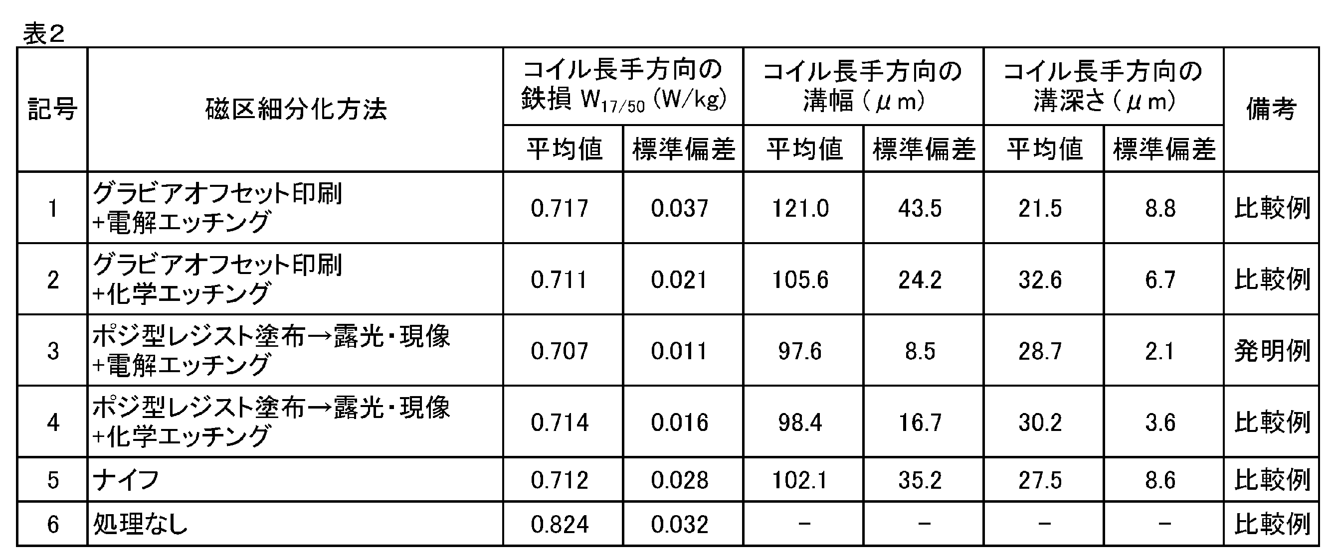
- the cold rolled steel sheet obtained as described above was subjected to magnetic domain refinement treatment by various methods shown in Table 2.
- a mesh provided on the plate roll is set so that uncoated portions extending at a width of 100 ⁇ m in the plate width direction are arranged at a pitch of 3 mm in the rolling direction, and the epoxy resin is used as a main component by using this mesh.
- a resist containing a novolak resin and a naphthoquinone diazide photosensitizer is roll-coated on a cold-rolled steel sheet, and a mask having a width of 100 ⁇ m and slits extending in the width direction of 3 mm is provided at a distance from the cold-rolled steel sheet.
- a mask having a width of 100 ⁇ m and slits extending in the width direction of 3 mm is provided at a distance from the cold-rolled steel sheet.
- the exposure was performed for 1 second at an illuminance of 100 mW / cm 2 using an ultrahigh pressure mercury lamp.
- the film thickness was 2 ⁇ m.
- the film was immersed in a potassium hydroxide solution for 60 seconds for development, and then dried with hot air at 120 ° C. for 20 seconds.
- a gravure-printed steel plate or a steel plate that was exposed and developed after applying a positive resist was subjected to electrolytic etching or chemical etching to form grooves.
- chemical etching after immersing in FeCl 3 for 30 seconds, pure water was washed.
- the resist was removed by immersion in an aqueous NaOH solution after the etching described above.
- grooves of 3 mm pitch were formed by pressing the knife edge against the steel sheet surface with a constant stress and pulling it in the sheet width direction.
- the width and depth of the grooves formed in the cold-rolled steel sheet as described above were measured at five points in the plate width direction at 30 positions in the coil longitudinal direction. Then, after performing the primary recrystallization annealing which served also as the decarburization annealing with the test piece which did not perform the magnetic domain fragmentation process, the annealing separation agent which mainly has MgO was apply
- test piece after final finish annealing thus obtained was measured for iron loss W 17/50 at a magnetic flux density of 1.7 T and an excitation frequency of 50 Hz in accordance with JIS C2550. The results of this measurement are also shown in Table 2.
- Example 2 Various resists shown in Table 3 were applied to the same cold-rolled steel sheet coils as those produced in Example 1.
- resists other than offset gravure printing are uniformly applied to the surface of the steel sheet by a roll coater, and use a light source shown in Table 3 and a mask having a slit or shielding part with a width of 100 ⁇ m, and an optical system for mirrors and lenses.
- Exposure was performed in a projection type via The projection magnification was set to the same magnification.
- the steel plate coated with the chemically amplified resist was subjected to heat treatment at 80 ° C. for 30 seconds. Subsequently, it developed with the developing solution suitable for a resist.
- a plate roll in which uncoated portions with a width of 100 ⁇ m were formed at a pitch of 3 mm in the rolling direction was produced, and an epoxy resin was printed on the steel sheet surface.
- test piece after final finish annealing thus obtained was measured for iron loss W 17/50 at a magnetic flux density of 1.7 T and an excitation frequency of 50 Hz in accordance with JIS C2550.
- the results are also shown in Table 3.
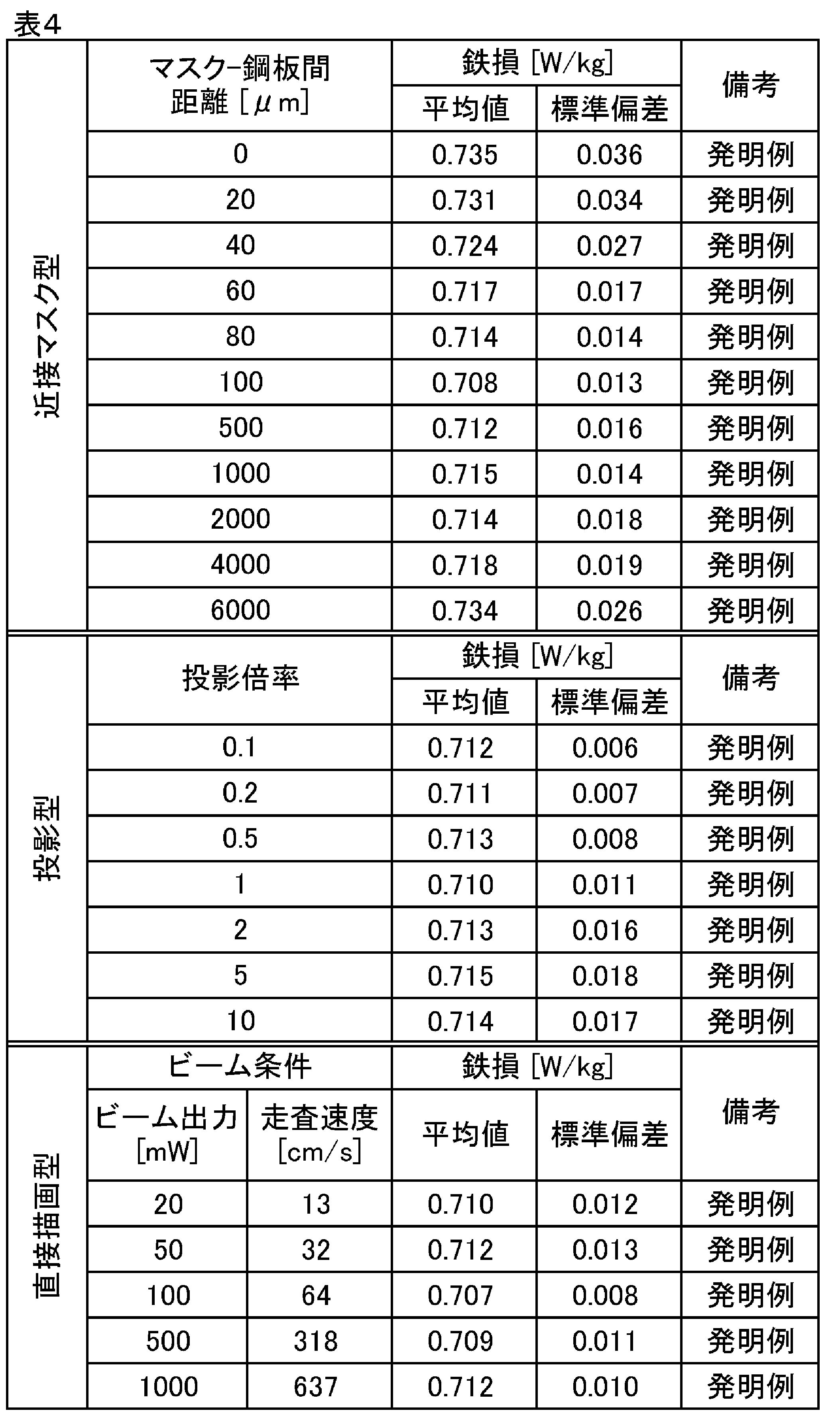
- Example 3 A cold-rolled steel sheet coil similar to that prepared in Example 1 was roll-coated with a positive resist mainly composed of a novolak resin and a naphthoquinone diazide-based photosensitizer at a film thickness of 3 ⁇ m and subjected to heat treatment at 100 ° C. for 30 seconds. did. Thereafter, one surface of the steel sheet was exposed under various conditions by three exposure methods of a proximity mask type, a projection type, and a direct drawing type.
- the proximity mask type a mask in which 100 ⁇ m wide slits extending in the plate width direction are cut at a pitch of 5 mm in the rolling direction is manufactured, and the distance between the mask and the steel plate is changed within the range shown in Table 4, and the illuminance is 50 mW / cm 2. For 3 seconds using an ultrahigh pressure mercury lamp.
- a plurality of masks are prepared so that a region extending in the plate width direction with a width of 100 ⁇ m is exposed at every 5 mm pitch in the rolling direction when reduced and enlarged projected on the steel plate surface at the magnification shown in Table 4.
- the image that passed through the mask was projected on the surface of the steel sheet at various projection magnifications through a lens and a mirror.
- the illuminance was adjusted to 50 mW / cm 2 on the steel plate surface, and the same area was exposed for 3 seconds.
- a semiconductor laser having a wavelength of 375 nm with various outputs is condensed using an optical system composed of a mirror and a lens so that the spot diameter on the surface of the steel sheet is 100 ⁇ m and scanned in the width direction of the sheet. This was repeated at a pitch of 5 mm in the rolling direction.
- Table 4 shows the conditions of the laser output and the scanning speed in the plate width direction.
- test pieces after final finish annealing thus obtained were measured for iron loss W 17/50 at a magnetic flux density of 1.7 T and an excitation frequency of 50 Hz in accordance with JIS C2550, and the results are also shown in Table 4.
Landscapes
- Chemical & Material Sciences (AREA)
- Engineering & Computer Science (AREA)
- Physics & Mathematics (AREA)
- Materials Engineering (AREA)
- Metallurgy (AREA)
- Organic Chemistry (AREA)
- Mechanical Engineering (AREA)
- Thermal Sciences (AREA)
- Crystallography & Structural Chemistry (AREA)
- General Physics & Mathematics (AREA)
- Spectroscopy & Molecular Physics (AREA)
- Manufacturing & Machinery (AREA)
- Electromagnetism (AREA)
- Chemical Kinetics & Catalysis (AREA)
- Electrochemistry (AREA)
- Dispersion Chemistry (AREA)
- Power Engineering (AREA)
- Manufacturing Of Steel Electrode Plates (AREA)
- Soft Magnetic Materials (AREA)
- ing And Chemical Polishing (AREA)
- Other Surface Treatments For Metallic Materials (AREA)
Abstract
Description
本発明は上記の知見に立脚するものである。
1.方向性電磁鋼板用素材に熱間圧延を施して熱延鋼板とし、
該熱延鋼板に1回または中間焼鈍を含む2回以上の冷間圧延を施して最終板厚を有する冷延鋼板とし、
前記冷延鋼板の片面または両面に、感光性樹脂を含むレジスト皮膜を塗布し、塗布した面を局所的に露光してパターニングを行い、現像によって板幅方向に連続または不連続な線状の地鉄露出部を形成し、
前記地鉄露出部が形成された鋼板を電解エッチングして、板幅方向に連続または不連続な線状の溝を形成し、
前記電解エッチング後の鋼板に一次再結晶焼鈍を施し、その後最終仕上げ焼鈍を施す方向性電磁鋼板の製造方法において、
前記電解エッチングにおいて、電極に投入する電流をI、電極の面積と同一面積の鋼板表面における地鉄露出部の面積をSとしたとき、地鉄露出部に対する電流密度ρ=I/Sが7.5A/cm2以上であることを特徴とする、方向性電磁鋼板の製造方法。
まず、発明者らが本発明を着想するに至った実験として、レジスト皮膜の塗布方法について検討を行った実験の説明を行う。
実験に使用した方向性電磁鋼板は、方向性電磁鋼用スラブを熱間圧延し、その後必要に応じて熱延板焼鈍を行った後、1回または中間焼鈍をはさむ2回の冷間圧延により最終製品板厚とし、その後、脱炭焼鈍ついで最終仕上げ焼鈍を施し、その後、上塗りコーティングを施して製造した。
かくして得られた製品板から試験片を切り出し、歪取り焼鈍を施した後、JIS C2550に記載の方法で鉄損W17/50を測定した。
その結果を表1に示す。なお、基本電流密度は、投入電流Iを電極の面積Rで除したI/R[A/cm2]で定義される電流密度である。

本発明に用いる方向性電磁鋼板用素材は、鋳造によってスラブとして供給する。鋳造の方法は特に限定しない。素材となるスラブの組成は、方向性電磁鋼板用として一般に用いられるものであれば特に限定しないが、例えば、Si:2~5mass%、C:0.002~0.10mass%、Mn:0.01~0.80mass%、Al:0.002~0.05mass%、N:0.003~0.02mass%を含有し、残部Feおよび不可避的不純物とすることができる。
さらに、1回または中間焼鈍を含む2回以上の冷間圧延を施し、冷延鋼板(以下、単に鋼板ともいう)とする。これらの方法は公知の方法で行えば良い。
このようにして得られた冷延鋼板の片面または両面に感光性樹脂を含むレジスト皮膜を塗布する。
上記露光時に、マスクを鋼板と接触させると、レジストに疵や剥離が生じ、電解エッチング時に意図しない領域がエッチングされることで鉄損の劣化をもたらす。そこで、本発明においては、マスクと鋼板は接触させずに露光を行う。
そのために、本発明における電解電流密度は7.5A/cm2以上とする。好ましくは12A/cm2以上、より好ましくは20A/cm2以上である。電解電流密度の上限は特に指定しないが、鋼板の発熱など避ける観点から1000A/cm2以下とするのが好ましい。
Si:3.0mass%、C:0.05mass%、Mn:0.03mass%、Al:0.02mass%、N:0.01mass%を含有し、残部Feおよび不可避的不純物からなる鋼スラブを、1400℃で加熱した後、熱間圧延して2.2mmの板厚とし、1100℃×60秒の熱延板焼鈍を施した後、冷間圧延して板厚1.8mmとし、1100℃×60秒の中間焼鈍を施した後、2回目の冷間圧延で0.23mmの最終板厚とした。
ここで、グラビアオフセット印刷では、版ロールに設けるメッシュを、板幅方向に100μm幅で延びる未塗布部が圧延方向に3mmピッチで並ぶように設定し、このメッシュを用いてエポキシ系樹脂を主成分とするレジストを冷延鋼板に印刷した。
その後、磁区細分化処理を施さなかった試験片とともに、脱炭焼鈍を兼ねた一次再結晶焼鈍を施したのち、MgOを主体とする焼鈍分離剤を塗布して最終仕上げ焼鈍を施した。
実施例1で作製したものと同様の冷延鋼板コイルに、表3に示す種々のレジストを塗布した。ここで、オフセットグラビア印刷以外のレジストは、ロールコータにて鋼板表面に均一塗布され、表3に示す光源と幅100μmのスリットまたは遮蔽部の形成されたマスクとを用い、ミラーおよびレンズの光学系を介した投影型で露光を施した。投影倍率は等倍とした。

実施例1で作製したものと同様の冷延鋼板コイルに、ノボラック樹脂とナフトキノンジアジド系感光剤を主成分とするポジ型レジストを膜厚3μmでロールコートし、100℃×30秒の熱処理を施した。その後、近接マスク型、投影型、直接描画型の3つの露光方法でそれぞれ種々の条件で鋼板片面に露光を施した。
2 光
3 光照射装置(光源)
4 ミラー
5 マスク部材
6 マスクと鋼板との距離:L
7 レンズ
Claims (7)
- 方向性電磁鋼板用素材に熱間圧延を施して熱延鋼板とし、
該熱延鋼板に1回または中間焼鈍を含む2回以上の冷間圧延を施して最終板厚を有する冷延鋼板とし、
前記冷延鋼板の片面または両面に、感光性樹脂を含むレジスト皮膜を塗布し、塗布した面を局所的に露光してパターニングを行い、現像によって板幅方向に連続または不連続な線状の地鉄露出部を形成し、
前記地鉄露出部が形成された鋼板を電解エッチングして、板幅方向に連続または不連続な線状の溝を形成し、
前記電解エッチング後の鋼板に一次再結晶焼鈍を施し、その後最終仕上げ焼鈍を施す方向性電磁鋼板の製造方法において、
前記電解エッチングにおいて、電極に投入する電流をI、電極の面積と同一面積の鋼板表面における地鉄露出部の面積をSとしたとき、地鉄露出部に対する電流密度ρ=I/Sが7.5A/cm2以上であることを特徴とする、方向性電磁鋼板の製造方法。 - 前記レジスト皮膜はポジ型レジストであり、前記パターニングは該ポジ型レジスト皮膜を塗布した面の溝形成領域を露光して行うことを特徴とする、請求項1に記載の方向性電磁鋼板の製造方法。
- 前記レジスト皮膜はネガ型レジストであり、前記パターニングは該ネガ型レジスト皮膜を塗布した面の非溝形成領域を露光して行うことを特徴とする、請求項1に記載の方向性電磁鋼板の製造方法。
- 前記レジスト皮膜は化学増幅型レジストであることを特徴とする、請求項2または3に記載の方向性電磁鋼板の製造方法。
- 前記パターニングの露光は、前記鋼板上で光を走査し、該光の照射により前記レジスト皮膜を変性させて行うことを特徴とする、請求項1~4のいずれか1項に記載の方向性電磁鋼板の製造方法。
- 前記パターニングの露光は、前記鋼板と離間して設置したマスクの開口部を通過した光を、前記鋼板に照射することにより行い、かつ、前記マスクと前記鋼板との距離が50μm以上5000μm以下であることを特徴とする、請求項1~4のいずれか1項に記載の方向性電磁鋼板の製造方法。
- 前記パターニングの露光は、レンズおよび/またはミラーを介して、前記鋼板と離間して設置したマスクの開口部を通過した光を、前記鋼板に照射することにより行うことを特徴とする、請求項1~4のいずれか1項に記載の方向性電磁鋼板の製造方法。
Priority Applications (6)
| Application Number | Priority Date | Filing Date | Title |
|---|---|---|---|
| CN201680009420.3A CN107208304B (zh) | 2015-02-10 | 2016-02-01 | 取向性电磁钢板的制造方法 |
| US15/548,836 US20180017868A1 (en) | 2015-02-10 | 2016-02-01 | Manufacturing method for grain-oriented electrical steel sheet |
| JP2016514792A JP6146535B2 (ja) | 2015-02-10 | 2016-02-01 | 方向性電磁鋼板の製造方法 |
| RU2017131493A RU2686711C2 (ru) | 2015-02-10 | 2016-02-01 | Способ производства листовой электротехнической стали с ориентированной структурой |
| EP16748883.2A EP3257973B1 (en) | 2015-02-10 | 2016-02-01 | Manufacturing method for grain oriented electrical steel sheet |
| KR1020177024601A KR20170109665A (ko) | 2015-02-10 | 2016-02-01 | 방향성 전자 강판의 제조 방법 |
Applications Claiming Priority (2)
| Application Number | Priority Date | Filing Date | Title |
|---|---|---|---|
| JP2015-024501 | 2015-02-10 | ||
| JP2015024501 | 2015-02-10 |
Publications (2)
| Publication Number | Publication Date |
|---|---|
| WO2016129235A1 true WO2016129235A1 (ja) | 2016-08-18 |
| WO2016129235A8 WO2016129235A8 (ja) | 2017-06-08 |
Family
ID=56615493
Family Applications (1)
| Application Number | Title | Priority Date | Filing Date |
|---|---|---|---|
| PCT/JP2016/000505 Ceased WO2016129235A1 (ja) | 2015-02-10 | 2016-02-01 | 方向性電磁鋼板の製造方法 |
Country Status (7)
| Country | Link |
|---|---|
| US (1) | US20180017868A1 (ja) |
| EP (1) | EP3257973B1 (ja) |
| JP (1) | JP6146535B2 (ja) |
| KR (1) | KR20170109665A (ja) |
| CN (1) | CN107208304B (ja) |
| RU (1) | RU2686711C2 (ja) |
| WO (1) | WO2016129235A1 (ja) |
Cited By (11)
| Publication number | Priority date | Publication date | Assignee | Title |
|---|---|---|---|---|
| JP2020090709A (ja) * | 2018-12-05 | 2020-06-11 | Jfeスチール株式会社 | 方向性電磁鋼板の鉄損改善方法およびその装置 |
| JP2020158882A (ja) * | 2019-03-19 | 2020-10-01 | Jfeスチール株式会社 | 方向性電磁鋼板およびその製造方法 |
| WO2021020028A1 (ja) * | 2019-07-31 | 2021-02-04 | Jfeスチール株式会社 | 線状溝形成方法および線状溝形成装置ならびに方向性電磁鋼板の製造方法 |
| WO2021020027A1 (ja) * | 2019-07-31 | 2021-02-04 | Jfeスチール株式会社 | 線状溝形成方法および方向性電磁鋼板の製造方法 |
| JP2021025072A (ja) * | 2019-08-01 | 2021-02-22 | 日本製鉄株式会社 | 方向性電磁鋼板、巻鉄芯、方向性電磁鋼板の製造方法、及び、巻鉄芯の製造方法 |
| WO2021229933A1 (ja) * | 2020-05-15 | 2021-11-18 | Jfeスチール株式会社 | 線状溝形成方法および方向性電磁鋼板の製造方法 |
| JP7040584B1 (ja) | 2020-10-06 | 2022-03-23 | Jfeスチール株式会社 | 金属ストリップ表面への溝形成方法、および方向性電磁鋼板の製造方法 |
| JP7040585B1 (ja) | 2020-10-06 | 2022-03-23 | Jfeスチール株式会社 | 金属ストリップ表面への溝形成方法、および方向性電磁鋼板の製造方法 |
| JP2022078119A (ja) * | 2019-11-18 | 2022-05-24 | 住友金属鉱山株式会社 | 磁歪部材及び磁歪部材の製造方法 |
| WO2022153605A1 (ja) * | 2021-01-18 | 2022-07-21 | Jfeスチール株式会社 | 方向性電磁鋼板およびその製造方法 |
| KR102956873B1 (ko) | 2020-10-06 | 2026-04-23 | 제이에프이 스틸 가부시키가이샤 | 금속 스트립 표면으로의 홈 형성 방법 및, 방향성 전자 강판의 제조 방법 |
Families Citing this family (7)
| Publication number | Priority date | Publication date | Assignee | Title |
|---|---|---|---|---|
| CN107012309B (zh) * | 2011-12-27 | 2020-03-10 | 杰富意钢铁株式会社 | 取向性电磁钢板的铁损改善装置 |
| CN107675190A (zh) * | 2017-08-21 | 2018-02-09 | 全球能源互联网研究院有限公司 | 一种提高超薄取向硅钢磁性能的方法 |
| EP3654355A1 (de) * | 2018-11-14 | 2020-05-20 | Siemens Aktiengesellschaft | Elektroblech mit strukturierter oberfläche zur domänenverfeinerung |
| DE102019201468B4 (de) | 2019-02-05 | 2025-05-15 | Carl Zeiss Smt Gmbh | Vorrichtung und Verfahren zum Reparieren einer fotolithographischen Maske |
| WO2021156980A1 (ja) * | 2020-02-05 | 2021-08-12 | 日本製鉄株式会社 | 方向性電磁鋼板 |
| US20230084111A1 (en) * | 2020-02-05 | 2023-03-16 | Nippon Steel Corporation | Grain oriented electrical steel sheet |
| JP7006851B1 (ja) * | 2020-05-19 | 2022-02-10 | Jfeスチール株式会社 | 方向性電磁鋼板およびその製造方法 |
Citations (5)
| Publication number | Priority date | Publication date | Assignee | Title |
|---|---|---|---|---|
| JPS62179105A (ja) * | 1986-02-03 | 1987-08-06 | Nippon Steel Corp | 低鉄損一方向性電磁鋼板の製造方法 |
| JPS6342332A (ja) * | 1986-08-06 | 1988-02-23 | Kawasaki Steel Corp | 低鉄損方向性電磁鋼板の製造方法 |
| JP2005123651A (ja) * | 2000-12-26 | 2005-05-12 | Toshiba Corp | レジスト膜の処理装置、およびレジストパターン形成方法 |
| WO2011162086A1 (ja) * | 2010-06-25 | 2011-12-29 | 新日本製鐵株式会社 | 一方向性電磁鋼板の製造方法 |
| JP2014171998A (ja) * | 2013-03-11 | 2014-09-22 | Jfe Steel Corp | 塗布方法および塗布装置 |
Family Cites Families (5)
| Publication number | Priority date | Publication date | Assignee | Title |
|---|---|---|---|---|
| KR930007313B1 (ko) * | 1990-08-01 | 1993-08-05 | 가와사끼세이데쓰 가부시끼가이샤 | 저 철손 방향성 전자강판의 제조방법 |
| JP3696156B2 (ja) * | 2000-12-26 | 2005-09-14 | 株式会社東芝 | 塗布膜の加熱装置、レジスト膜の処理方法 |
| JP5994838B2 (ja) * | 2014-12-11 | 2016-09-21 | Jfeスチール株式会社 | 冷延鋼帯の線状溝形成方法および方向性電磁鋼板の製造方法 |
| US20180057956A1 (en) * | 2014-12-25 | 2018-03-01 | Jfe Steel Corporation | Method for forming linear groove on steel strip and method for manufacturing grain-oriented electrical steel sheet |
| JP6332185B2 (ja) * | 2015-07-22 | 2018-05-30 | Jfeスチール株式会社 | 鋼板表面に線状溝を形成する方法 |
-
2016
- 2016-02-01 RU RU2017131493A patent/RU2686711C2/ru active
- 2016-02-01 KR KR1020177024601A patent/KR20170109665A/ko not_active Ceased
- 2016-02-01 CN CN201680009420.3A patent/CN107208304B/zh active Active
- 2016-02-01 EP EP16748883.2A patent/EP3257973B1/en active Active
- 2016-02-01 WO PCT/JP2016/000505 patent/WO2016129235A1/ja not_active Ceased
- 2016-02-01 US US15/548,836 patent/US20180017868A1/en not_active Abandoned
- 2016-02-01 JP JP2016514792A patent/JP6146535B2/ja active Active
Patent Citations (5)
| Publication number | Priority date | Publication date | Assignee | Title |
|---|---|---|---|---|
| JPS62179105A (ja) * | 1986-02-03 | 1987-08-06 | Nippon Steel Corp | 低鉄損一方向性電磁鋼板の製造方法 |
| JPS6342332A (ja) * | 1986-08-06 | 1988-02-23 | Kawasaki Steel Corp | 低鉄損方向性電磁鋼板の製造方法 |
| JP2005123651A (ja) * | 2000-12-26 | 2005-05-12 | Toshiba Corp | レジスト膜の処理装置、およびレジストパターン形成方法 |
| WO2011162086A1 (ja) * | 2010-06-25 | 2011-12-29 | 新日本製鐵株式会社 | 一方向性電磁鋼板の製造方法 |
| JP2014171998A (ja) * | 2013-03-11 | 2014-09-22 | Jfe Steel Corp | 塗布方法および塗布装置 |
Non-Patent Citations (1)
| Title |
|---|
| See also references of EP3257973A4 * |
Cited By (27)
| Publication number | Priority date | Publication date | Assignee | Title |
|---|---|---|---|---|
| JP2020090709A (ja) * | 2018-12-05 | 2020-06-11 | Jfeスチール株式会社 | 方向性電磁鋼板の鉄損改善方法およびその装置 |
| JP7010321B2 (ja) | 2019-03-19 | 2022-02-10 | Jfeスチール株式会社 | 方向性電磁鋼板およびその製造方法 |
| JP2020158882A (ja) * | 2019-03-19 | 2020-10-01 | Jfeスチール株式会社 | 方向性電磁鋼板およびその製造方法 |
| JP2021025061A (ja) * | 2019-07-31 | 2021-02-22 | Jfeスチール株式会社 | 線状溝形成方法および方向性電磁鋼板の製造方法 |
| JP7056758B2 (ja) | 2019-07-31 | 2022-04-19 | Jfeスチール株式会社 | 線状溝形成方法および線状溝形成装置ならびに方向性電磁鋼板の製造方法 |
| JPWO2021020028A1 (ja) * | 2019-07-31 | 2021-09-13 | Jfeスチール株式会社 | 線状溝形成方法および線状溝形成装置ならびに方向性電磁鋼板の製造方法 |
| WO2021020027A1 (ja) * | 2019-07-31 | 2021-02-04 | Jfeスチール株式会社 | 線状溝形成方法および方向性電磁鋼板の製造方法 |
| US12404563B2 (en) | 2019-07-31 | 2025-09-02 | Jfe Steel Corporation | Linear groove formation method and method for producing grain-oriented electrical steel sheet |
| WO2021020028A1 (ja) * | 2019-07-31 | 2021-02-04 | Jfeスチール株式会社 | 線状溝形成方法および線状溝形成装置ならびに方向性電磁鋼板の製造方法 |
| US12195816B2 (en) | 2019-07-31 | 2025-01-14 | Jfe Steel Corporation | Linear groove formation method and linear groove forming apparatus, and method for manufacturing grain-oriented electrical steel sheet |
| JP2021025072A (ja) * | 2019-08-01 | 2021-02-22 | 日本製鉄株式会社 | 方向性電磁鋼板、巻鉄芯、方向性電磁鋼板の製造方法、及び、巻鉄芯の製造方法 |
| JP7277755B2 (ja) | 2019-08-01 | 2023-05-19 | 日本製鉄株式会社 | 方向性電磁鋼板、巻鉄芯、方向性電磁鋼板の製造方法、及び、巻鉄芯の製造方法 |
| JP7732373B2 (ja) | 2019-11-18 | 2025-09-02 | 住友金属鉱山株式会社 | 磁歪部材及び磁歪部材の製造方法 |
| JP2022078119A (ja) * | 2019-11-18 | 2022-05-24 | 住友金属鉱山株式会社 | 磁歪部材及び磁歪部材の製造方法 |
| WO2021229933A1 (ja) * | 2020-05-15 | 2021-11-18 | Jfeスチール株式会社 | 線状溝形成方法および方向性電磁鋼板の製造方法 |
| JP2021179007A (ja) * | 2020-05-15 | 2021-11-18 | Jfeスチール株式会社 | 線状溝形成方法および方向性電磁鋼板の製造方法 |
| WO2022074882A1 (ja) * | 2020-10-06 | 2022-04-14 | Jfeスチール株式会社 | 金属ストリップ表面への溝形成方法、および方向性電磁鋼板の製造方法 |
| JP2022061431A (ja) * | 2020-10-06 | 2022-04-18 | Jfeスチール株式会社 | 金属ストリップ表面への溝形成方法、および方向性電磁鋼板の製造方法 |
| JP2022061432A (ja) * | 2020-10-06 | 2022-04-18 | Jfeスチール株式会社 | 金属ストリップ表面への溝形成方法、および方向性電磁鋼板の製造方法 |
| WO2022074883A1 (ja) * | 2020-10-06 | 2022-04-14 | Jfeスチール株式会社 | 金属ストリップ表面への溝形成方法、および方向性電磁鋼板の製造方法 |
| JP7040585B1 (ja) | 2020-10-06 | 2022-03-23 | Jfeスチール株式会社 | 金属ストリップ表面への溝形成方法、および方向性電磁鋼板の製造方法 |
| JP7040584B1 (ja) | 2020-10-06 | 2022-03-23 | Jfeスチール株式会社 | 金属ストリップ表面への溝形成方法、および方向性電磁鋼板の製造方法 |
| US12467104B2 (en) | 2020-10-06 | 2025-11-11 | Jfe Steel Corporation | Method for forming grooves on metal strip surface and method for manufacturing grain-oriented electrical steel sheet |
| KR102956873B1 (ko) | 2020-10-06 | 2026-04-23 | 제이에프이 스틸 가부시키가이샤 | 금속 스트립 표면으로의 홈 형성 방법 및, 방향성 전자 강판의 제조 방법 |
| WO2022153605A1 (ja) * | 2021-01-18 | 2022-07-21 | Jfeスチール株式会社 | 方向性電磁鋼板およびその製造方法 |
| JP2022110540A (ja) * | 2021-01-18 | 2022-07-29 | Jfeスチール株式会社 | 方向性電磁鋼板およびその製造方法 |
| JP7435486B2 (ja) | 2021-01-18 | 2024-02-21 | Jfeスチール株式会社 | 方向性電磁鋼板およびその製造方法 |
Also Published As
| Publication number | Publication date |
|---|---|
| JP6146535B2 (ja) | 2017-06-14 |
| JPWO2016129235A1 (ja) | 2017-04-27 |
| RU2017131493A (ru) | 2019-03-12 |
| KR20170109665A (ko) | 2017-09-29 |
| CN107208304B (zh) | 2019-03-15 |
| RU2686711C2 (ru) | 2019-04-30 |
| WO2016129235A8 (ja) | 2017-06-08 |
| EP3257973A4 (en) | 2018-03-21 |
| RU2017131493A3 (ja) | 2019-03-12 |
| EP3257973B1 (en) | 2021-08-18 |
| US20180017868A1 (en) | 2018-01-18 |
| CN107208304A (zh) | 2017-09-26 |
| EP3257973A1 (en) | 2017-12-20 |
Similar Documents
| Publication | Publication Date | Title |
|---|---|---|
| JP6146535B2 (ja) | 方向性電磁鋼板の製造方法 | |
| JP6172403B2 (ja) | 線状溝形成方法および線状溝形成装置 | |
| RU2569269C1 (ru) | Текстурированная электротехническая листовая сталь и способ её изготовления | |
| JP5994838B2 (ja) | 冷延鋼帯の線状溝形成方法および方向性電磁鋼板の製造方法 | |
| JP6394617B2 (ja) | 低鉄損方向性電磁鋼板を製造するための設備列及び低鉄損方向性電磁鋼板の製造方法 | |
| JP6977702B2 (ja) | 方向性電磁鋼板の鉄損改善方法およびその装置 | |
| JPWO2013099272A1 (ja) | 方向性電磁鋼板およびその製造方法 | |
| CN103025896B (zh) | 单向性电磁钢板的制造方法 | |
| JP2015071815A (ja) | 方向性電磁鋼板の製造方法 | |
| JPH11293340A (ja) | 低鉄損方向性電磁鋼板及びその製造方法 | |
| JPH0488121A (ja) | 特性値のばらつきが小さい低鉄損方向性電磁鋼板の製造方法 | |
| KR930007313B1 (ko) | 저 철손 방향성 전자강판의 제조방법 | |
| JPS62179105A (ja) | 低鉄損一方向性電磁鋼板の製造方法 | |
| US20180057956A1 (en) | Method for forming linear groove on steel strip and method for manufacturing grain-oriented electrical steel sheet | |
| JP7040584B1 (ja) | 金属ストリップ表面への溝形成方法、および方向性電磁鋼板の製造方法 | |
| JP2007308770A (ja) | 低鉄損方向性電磁鋼板およびその製造方法 | |
| JP3663784B2 (ja) | 低鉄損方向性電磁鋼板の製造方法 | |
| JP2025177250A (ja) | 磁区細分化方向性電磁鋼板の製造方法および製造設備 | |
| JPH0230718A (ja) | 抵鉄損方向性電磁鋼板の製造方法 | |
| JPS61117285A (ja) | 低鉄損方向性けい素鋼板の製造方法 |
Legal Events
| Date | Code | Title | Description |
|---|---|---|---|
| ENP | Entry into the national phase |
Ref document number: 2016514792 Country of ref document: JP Kind code of ref document: A |
|
| 121 | Ep: the epo has been informed by wipo that ep was designated in this application |
Ref document number: 16748883 Country of ref document: EP Kind code of ref document: A1 |
|
| WWE | Wipo information: entry into national phase |
Ref document number: 15548836 Country of ref document: US |
|
| REEP | Request for entry into the european phase |
Ref document number: 2016748883 Country of ref document: EP |
|
| NENP | Non-entry into the national phase |
Ref country code: DE |
|
| ENP | Entry into the national phase |
Ref document number: 20177024601 Country of ref document: KR Kind code of ref document: A |
|
| ENP | Entry into the national phase |
Ref document number: 2017131493 Country of ref document: RU Kind code of ref document: A |