WO2016136244A1 - プライマー組成物、接着方法、および電気・電子部品 - Google Patents
プライマー組成物、接着方法、および電気・電子部品 Download PDFInfo
- Publication number
- WO2016136244A1 WO2016136244A1 PCT/JP2016/000960 JP2016000960W WO2016136244A1 WO 2016136244 A1 WO2016136244 A1 WO 2016136244A1 JP 2016000960 W JP2016000960 W JP 2016000960W WO 2016136244 A1 WO2016136244 A1 WO 2016136244A1
- Authority
- WO
- WIPO (PCT)
- Prior art keywords
- group
- primer
- primer composition
- substrate
- formula
- Prior art date
- Legal status (The legal status is an assumption and is not a legal conclusion. Google has not performed a legal analysis and makes no representation as to the accuracy of the status listed.)
- Ceased
Links
Images

Classifications
-
- C—CHEMISTRY; METALLURGY
- C08—ORGANIC MACROMOLECULAR COMPOUNDS; THEIR PREPARATION OR CHEMICAL WORKING-UP; COMPOSITIONS BASED THEREON
- C08L—COMPOSITIONS OF MACROMOLECULAR COMPOUNDS
- C08L83/00—Compositions of macromolecular compounds obtained by reactions forming in the main chain of the macromolecule a linkage containing silicon with or without sulfur, nitrogen, oxygen or carbon only; Compositions of derivatives of such polymers
- C08L83/10—Block- or graft-copolymers containing polysiloxane sequences
-
- C—CHEMISTRY; METALLURGY
- C09—DYES; PAINTS; POLISHES; NATURAL RESINS; ADHESIVES; COMPOSITIONS NOT OTHERWISE PROVIDED FOR; APPLICATIONS OF MATERIALS NOT OTHERWISE PROVIDED FOR
- C09D—COATING COMPOSITIONS, e.g. PAINTS, VARNISHES OR LACQUERS; FILLING PASTES; CHEMICAL PAINT OR INK REMOVERS; INKS; CORRECTING FLUIDS; WOODSTAINS; PASTES OR SOLIDS FOR COLOURING OR PRINTING; USE OF MATERIALS THEREFOR
- C09D183/00—Coating compositions based on macromolecular compounds obtained by reactions forming in the main chain of the macromolecule a linkage containing silicon, with or without sulfur, nitrogen, oxygen, or carbon only; Coating compositions based on derivatives of such polymers
- C09D183/10—Block or graft copolymers containing polysiloxane sequences
-
- C—CHEMISTRY; METALLURGY
- C09—DYES; PAINTS; POLISHES; NATURAL RESINS; ADHESIVES; COMPOSITIONS NOT OTHERWISE PROVIDED FOR; APPLICATIONS OF MATERIALS NOT OTHERWISE PROVIDED FOR
- C09D—COATING COMPOSITIONS, e.g. PAINTS, VARNISHES OR LACQUERS; FILLING PASTES; CHEMICAL PAINT OR INK REMOVERS; INKS; CORRECTING FLUIDS; WOODSTAINS; PASTES OR SOLIDS FOR COLOURING OR PRINTING; USE OF MATERIALS THEREFOR
- C09D5/00—Coating compositions, e.g. paints, varnishes or lacquers, characterised by their physical nature or the effects produced; Filling pastes
-
- C—CHEMISTRY; METALLURGY
- C09—DYES; PAINTS; POLISHES; NATURAL RESINS; ADHESIVES; COMPOSITIONS NOT OTHERWISE PROVIDED FOR; APPLICATIONS OF MATERIALS NOT OTHERWISE PROVIDED FOR
- C09D—COATING COMPOSITIONS, e.g. PAINTS, VARNISHES OR LACQUERS; FILLING PASTES; CHEMICAL PAINT OR INK REMOVERS; INKS; CORRECTING FLUIDS; WOODSTAINS; PASTES OR SOLIDS FOR COLOURING OR PRINTING; USE OF MATERIALS THEREFOR
- C09D5/00—Coating compositions, e.g. paints, varnishes or lacquers, characterised by their physical nature or the effects produced; Filling pastes
- C09D5/002—Priming paints
-
- C—CHEMISTRY; METALLURGY
- C09—DYES; PAINTS; POLISHES; NATURAL RESINS; ADHESIVES; COMPOSITIONS NOT OTHERWISE PROVIDED FOR; APPLICATIONS OF MATERIALS NOT OTHERWISE PROVIDED FOR
- C09D—COATING COMPOSITIONS, e.g. PAINTS, VARNISHES OR LACQUERS; FILLING PASTES; CHEMICAL PAINT OR INK REMOVERS; INKS; CORRECTING FLUIDS; WOODSTAINS; PASTES OR SOLIDS FOR COLOURING OR PRINTING; USE OF MATERIALS THEREFOR
- C09D7/00—Features of coating compositions, not provided for in group C09D5/00; Processes for incorporating ingredients in coating compositions
- C09D7/40—Additives
-
- C—CHEMISTRY; METALLURGY
- C08—ORGANIC MACROMOLECULAR COMPOUNDS; THEIR PREPARATION OR CHEMICAL WORKING-UP; COMPOSITIONS BASED THEREON
- C08L—COMPOSITIONS OF MACROMOLECULAR COMPOUNDS
- C08L2203/00—Applications
- C08L2203/20—Applications use in electrical or conductive gadgets
-
- H—ELECTRICITY
- H10—SEMICONDUCTOR DEVICES; ELECTRIC SOLID-STATE DEVICES NOT OTHERWISE PROVIDED FOR
- H10W—GENERIC PACKAGES, INTERCONNECTIONS, CONNECTORS OR OTHER CONSTRUCTIONAL DETAILS OF DEVICES COVERED BY CLASS H10
- H10W72/00—Interconnections or connectors in packages
- H10W72/851—Dispositions of multiple connectors or interconnections
- H10W72/874—On different surfaces
- H10W72/884—Die-attach connectors and bond wires
-
- H—ELECTRICITY
- H10—SEMICONDUCTOR DEVICES; ELECTRIC SOLID-STATE DEVICES NOT OTHERWISE PROVIDED FOR
- H10W—GENERIC PACKAGES, INTERCONNECTIONS, CONNECTORS OR OTHER CONSTRUCTIONAL DETAILS OF DEVICES COVERED BY CLASS H10
- H10W74/00—Encapsulations, e.g. protective coatings
-
- H—ELECTRICITY
- H10—SEMICONDUCTOR DEVICES; ELECTRIC SOLID-STATE DEVICES NOT OTHERWISE PROVIDED FOR
- H10W—GENERIC PACKAGES, INTERCONNECTIONS, CONNECTORS OR OTHER CONSTRUCTIONAL DETAILS OF DEVICES COVERED BY CLASS H10
- H10W90/00—Package configurations
- H10W90/701—Package configurations characterised by the relative positions of pads or connectors relative to package parts
- H10W90/721—Package configurations characterised by the relative positions of pads or connectors relative to package parts of bump connectors
- H10W90/724—Package configurations characterised by the relative positions of pads or connectors relative to package parts of bump connectors between a chip and a stacked insulating package substrate, interposer or RDL
Definitions
- the present invention relates to a primer composition, an adhesion method using the composition, and an electric / electronic component using the composition.
- the optical semiconductor element is sealed with a cured silicone to improve the reliability.
- a hydrosilylation reaction curable silicone composition is used.
- the silicone cured product obtained by curing the composition is a base material such as an optical semiconductor element, a packaging material, and a substrate. Adhesiveness to was not sufficient. In particular, a hardened silicone cured product with less surface tack and less adhesion of dust or the like has insufficient adhesion to the substrate.
- the base material is pretreated with a primer composition in order to improve the adhesiveness of the silicone cured product to the base material.
- the primer composition include a primer composition comprising an acrylic polymer, a silanol condensation catalyst, and a silane coupling agent (see Patent Document 1), an organosiloxane oligomer having an epoxy group and a silicon atom-bonded alkoxy group, and an organic solvent.
- a primer composition comprising a primer composition (see Patent Document 2), a silane coupling agent, a Lewis acidic organoaluminum compound, and an organic solvent (see Patent Document 3) is known.
- An object of the present invention is to provide a primer composition capable of improving the adhesiveness of a silicone cured product to a base material such as an optical semiconductor element, a package material, and a substrate, and suppressing peeling and cracking of the silicone cured product due to heat cycle. It is to provide.
- Another object of the present invention is to provide an adhesion method capable of improving the adhesion of the silicone cured product to the substrate and suppressing the peeling and cracking of the silicone cured product due to heat cycle.
- another object of the present invention is to provide an electrical / electronic component in which the adhesiveness of the silicone cured product to the substrate is improved, and peeling and cracking of the silicone cured product due to heat cycle are suppressed.
- the primer composition of the present invention comprises: (A) Average unit formula: (R 1 2 SiO 2/2 ) a (R 2 SiO 3/2 ) b (In the formula, R 1 and R 2 are each independently an alkyl group having 1 to 12 carbon atoms, an aryl group having 6 to 20 carbon atoms, or an aralkyl group having 7 to 20 carbon atoms, and a is 0.
- An organosiloxane block copolymer It consists of (B) a curing catalyst (amount that promotes curing of the present composition) and (C) an arbitrary amount of an organic solvent.
- the adhesion method of the present invention is characterized in that the primer composition is applied onto a substrate, the organic solvent is removed, and then the curable silicone composition is applied onto the obtained primer layer and cured. .
- the electric / electronic component of the present invention comprises an electric / electronic substrate, a primer layer on the substrate, and a cured silicone product on the primer layer, and the primer layer is formed of the primer composition described above. It is characterized by that.
- the primer composition of the present invention can improve the adhesiveness of the silicone cured product to a substrate such as an optical semiconductor element, a packaging material, or a substrate, and can suppress peeling and cracking of the silicone cured product due to heat cycle.
- the adhesion method of this invention can improve the adhesiveness of the silicone hardened
- the electrical / electronic component of the present invention can improve the adhesiveness of the silicone cured product to the substrate, and can suppress peeling and cracking of the silicone cured product due to heat cycle.
- COB chip-on-board
- COB chip on board
- the (A) component organosiloxane block copolymer has an average unit formula: (R 1 2 SiO 2/2 ) a (R 2 SiO 3/2 ) b It is represented by
- R 1 and R 2 are each independently an alkyl group having 1 to 12 carbon atoms, an aryl group having 6 to 20 carbon atoms, or an aralkyl group having 7 to 20 carbon atoms. Specifically, methyl group, ethyl group, propyl group, isopropyl group, butyl group, isobutyl group, tert-butyl group, pentyl group, neopentyl group, hexyl group, cyclohexyl group, octyl group, nonyl group, decyl group, etc.
- R 1 is preferably an alkyl group and / or an aryl group, and particularly preferably a methyl group and / or a phenyl group.
- R 2 is preferably an aryl group, and particularly preferably a phenyl group.
- a is a number from 0.40 to 0.90, and preferably a is a number from 0.50 to 0.90, or a number from 0.60 to 0.90.
- b is a number from 0.10 to 0.60, preferably a number from 0.10 to 0.50, or a number from 0.10 to 0.40.
- a + b + c 1.00.
- component (A) has the formula: [R 2 SiO 3/2 ]
- a resinous siloxane block represented by the formula: -(R 1 2 SiO 2/2 ) n- Are linked by a linear siloxane block represented by
- R 2 is an alkyl group having 1 to 12 carbon atoms, an aryl group having 6 to 20 carbon atoms, or an aralkyl group having 7 to 20 carbon atoms, Examples are groups.
- the weight average molecular weight of the resinous siloxane block is not limited, but is preferably at least 500. This means that the resinous siloxane block is composed of at least three or more trisiloxane units represented by the formula: R 2 SiO 3/2 .
- the weight average molecular weight is derived from the raw resin siloxane, and the raw resin siloxane can be measured by gel permeation chromatography (GPC).
- each R 1 independently represents an alkyl group having 1 to 12 carbon atoms, an aryl group having 6 to 20 carbon atoms, or an aralkyl group having 7 to 20 carbon atoms. And the same groups as described above are exemplified.
- the organosiloxane block copolymer of component (A) is composed of a disiloxy [R 1 2 SiO 2/2 ] unit and a trisiloxy [R 2 SiO 3/2 ] unit, and more preferably 0.5 to 35.0 mol%.
- Examples of the alkoxy group include alkoxy groups having 1 to 4 carbon atoms such as a methoxy group, an ethoxy group, a propoxy group, an isopropoxy group, a butoxy group, an isobutoxy group, and a tert-butoxy group.
- This silicon atom-bonded hydroxyl group or silicon atom-bonded alkoxy group is present on any siloxy unit in the organosiloxane block copolymer, and this silicon atom-bonded hydroxyl group or silicon atom-bonded alkoxy group reacts to form the composition. It can be cured.
- the molar fraction of the disiloxy [R 1 2 SiO 2/2 ] unit and the trisiloxy [R 2 SiO 3/2 ] unit in the organosiloxane block copolymer of the component (A), and the silicon atom-bonded hydroxyl group in the organosiloxane block copolymer can be measured by 29 Si-nuclear magnetic resonance spectrum (NMR).
- the component (A) is solid at 25 ° C. and has a softening point of 200 ° C. or less.
- the upper limit with a preferable softening point is 150 degrees C or less, or 100 degrees C or less, On the other hand, the preferable minimum is 30 degrees C or more, or 50 degrees C or more.
- the molecular weight of the component (A) is not limited, but preferably the weight average molecular weight is 20,000 or more, preferably 40,000 or more.
- the phase-separated linear siloxane block forms a “soft” polymer block
- the phase-separated “soft” polymer block and the “hard” polymer block have different glass transition temperatures (T g ), specifically Specifically, a “soft” polymer block having a lower T g , such as less than 25 ° C., less than 0 ° C., or less than ⁇ 20 ° C., and a higher T g such as greater than 30 ° C., greater than 40 ° C., or greater than 50 ° C. It consists of a “hard” polymer block.
- the silicone cured product obtained by adhering a base material such as an optical semiconductor element, a packaging material, or a substrate through a primer layer formed of the present composition is subjected to a heat cycle, the primer layer relaxes the stress and Peeling and cracking of the cured silicone can be suppressed.
- organosiloxane block copolymer of component (A) is not limited, and for example, it is prepared by the method described in JP-T-2013-540169 and JP-T-2013-544295.
- Component (B) is a curing catalyst for accelerating the curing of the composition, and preferably a condensation reaction catalyst.
- condensation reaction catalysts include organic tin compounds such as dibutyltin dilaurate, dibutyltin diacetate, tin octenoate, dibutyltin dioctate, tin laurate; tetrabutyl titanate, tetrapropyl titanate, dibutoxybis (ethylacetoacetate), etc.
- Organic titanium compounds such as: tetrabutyl zirconate, tetrakis (acetylacetonate) zirconium, tetraisobutyl zirconate, butoxytris (acetylacetonate) zirconium, zirconium naphthenate, zirconium octylate, zirconium 2-ethylhexanoate, etc.
- the content of the component (B) is an amount that accelerates the curing of the present composition.
- the content is preferably 0.005 to 0.5 parts by mass with respect to 100 parts by mass of the component (A). Within the range, or within the range of 0.01 to 0.5 parts by mass. This is because the composition obtained can be sufficiently cured when the content of the component (B) is not less than the lower limit of the above range, and on the other hand, the composition obtained when not more than the upper limit of the above range. This is because the mechanical properties and optical properties of the primer layer obtained by curing the product are not impaired.
- the organic solvent of component (C) is a component for dissolving the solid component (A) at 25 ° C. and improving the coating property of the present composition.
- organic solvents include aliphatic hydrocarbon solvents such as n-heptane, n-hexane, isooctane, cyclopentane, and cyclohexane; alcohol solvents such as ethanol, propanol, butanol, and cyclohexanol; diethyl ether, tetrahydrofuran, Ether solvents such as 1,4-dioxane; ketone solvents such as acetone and methyl isobutyl ketone; ester solvents such as ethyl acetate and butyl acetate; aromatic hydrocarbon solvents such as toluene and xylene; aromatics such as pyridine Heterocyclic solvents are exemplified.
- component (A) can be sufficiently dissolved, component (C) preferably contains an aromatic hydrocarbon solvent, and since this composition can be uniformly applied to a substrate, component (C) is aromatic.
- a mixed solvent of a hydrocarbon solvent and an aliphatic hydrocarbon solvent is preferable.
- the content of the component (C) is an amount that can be arbitrarily determined in consideration of the coating workability and the drying workability of the composition, and specifically, 70% by mass or more of the entire composition, preferably Is an amount in the range of 70 to 99.9% by mass or in the range of 80 to 99.9% by mass.
- alkenyl group-containing silane coupling agents such as vinyltrimethoxysilane, vinyltriethoxysilane, allyltrimethoxysilane, and allyltriethoxysilane; 3-glycidoxypropyltrimethoxysilane , Epoxy group-containing silane coupling agents such as 2- (3,4-epoxycyclohexyl) ethyltrimethoxysilane; methacrylic or acrylic groups such as 3-methacryloxypropyltrimethoxysilane and 3-acryloxypropyltrimethoxysilane Silane coupling agent; containing amino group-containing silane coupling agent such as 3-aminopropyltrimethoxysilane, 3-aminopropyltriethoxysilane, N- (2-ethylamino) -3-aminopropyltrimethoxysilane, etc. May be.
- the content of the silane coupling agent is not limited, but
- a catalyst for hydrosilylation reaction is added to increase the curability and adhesion with the primer layer. It may be contained. Examples of such a hydrosilylation reaction catalyst include a platinum-based catalyst, a rhodium-based catalyst, and a palladium-based catalyst, and a platinum-based catalyst is preferable because curing of the composition can be remarkably accelerated.
- platinum-based catalyst examples include platinum fine powder, chloroplatinic acid, alcohol solution of chloroplatinic acid, platinum-alkenylsiloxane complex, platinum-olefin complex, and platinum-carbonyl complex, and platinum-alkenylsiloxane complex is particularly preferable. .
- alkenylsiloxane examples include 1,3-divinyl-1,1,3,3-tetramethyldisiloxane, 1,3,5,7-tetramethyl-1,3,5,7-tetravinylcyclotetrasiloxane, Examples thereof include alkenyl siloxanes in which part of the methyl groups of these alkenyl siloxanes are substituted with ethyl groups, phenyl groups, and the like, and alkenyl siloxanes in which the vinyl groups of these alkenyl siloxanes are substituted with allyl groups, hexenyl groups, and the like.
- 1,3-divinyl-1,1,3,3-tetramethyldisiloxane is preferred because the platinum-alkenylsiloxane complex has good stability.
- the content of the hydrosilylation catalyst is preferably such that the metal atoms are in the range of 0.01 to 10,000 ppm in terms of mass unit with respect to the entire composition.
- the bonding method of the present invention will be described in detail.
- the primer composition is applied onto a substrate.
- the base material for electricity / electronic is not limited, and examples thereof include an optical semiconductor element, a package material, and a substrate.
- the material of the base material is not limited, for example, metal materials such as aluminum, copper, nickel and aluminum nitride; metal oxide materials such as glass and sapphire; imide resin, bismaleimide / triazine resin, glass fiber-containing epoxy resin , Paper phenol resin, bakelite, polyethylene terephthalate resin, polybutylene terephthalate resin, polyacrylonitrile resin, polycarbonate resin, fluorine resin, polyimide resin, polyphenylene sulfide resin, aramid resin, polyether ether resin, polyether imide resin, liquid crystal polymer, poly Examples thereof include organic materials such as ether sulfone resin, cycloolefin resin, silicone rubber, and silicone resin.
- the application amount of the primer composition is usually 30 to 100 g / m 2 , preferably 10 to 50 g / m 2 . This is because a primer layer having a sufficient thickness cannot be formed when the amount is less than the above lower limit, and strong adhesion cannot be achieved. If the above upper limit is exceeded, the primer layer becomes too thick and it is difficult to control the thickness of the curable silicone composition to be adhered.
- the primer composition As a method for applying the primer composition, conventionally known methods such as spraying, brushing, and dipping can be applied.
- the method for removing the organic solvent is not limited, and a well-known method such as a method of drying at room temperature, a method of drying by blowing air, a method of forcibly evaporating the organic solvent by heating, a method of drying by infrared irradiation, etc. Can be used.
- the primer layer In the process of removing the organic solvent, the primer layer may be cured, but may be cured at the same time when the curable silicone composition is subsequently cured.
- the curable silicone composition is applied and cured on the primer layer of the substrate.
- the curable silicone composition is not limited, but is preferably a hydrolyzed reaction curable silicone composition.
- This hydrosilylation reaction curable silicone composition is, for example, (I) an organopolysiloxane having at least two alkenyl groups in one molecule; (II) An organopolysiloxane having at least two silicon-bonded hydrogen atoms in one molecule, and (III) a catalyst for hydrosilylation reaction.
- alkenyl group in the component (I) examples include a vinyl group, an allyl group, a butenyl group, a pentenyl group, and a hexenyl group.
- an alkyl group such as methyl group, ethyl group, propyl group, butyl group, pentyl group, hexyl group, heptyl group; cyclopentyl group, cyclohexyl
- a cycloalkyl group such as a phenyl group; an aryl group such as a phenyl group, a tolyl group, a xylyl group and a naphthyl group; an aralkyl group such as a benzyl group, a phenethyl group and a 3-phenylpropyl group; a chloromethyl group, a 3-chloropropyl
- the molecular structure of the component (I) is not limited, and examples thereof include linear, cyclic, partially branched linear, and branched.
- the viscosity of the component (I) is not limited, and is preferably in the range of 20 to 100,000 mPa ⁇ s at 25 ° C., or in the range of 100 to 10,000 mPa ⁇ s.
- an alkyl group such as a methyl group, an ethyl group, a propyl group, a butyl group, a pentyl group, a hexyl group, a heptyl group; a cyclopentyl group, a cyclohexyl group, etc.
- Cycloalkyl group aryl group such as phenyl group, tolyl group, xylyl group, naphthyl group; aralkyl group such as benzyl group, phenethyl group, 3-phenylpropyl group; chloromethyl group, 3-chloropropyl group, 3, 3, Examples thereof include halogenated alkyl groups such as 3-trifluoropropyl group and nonafluorobutylethyl group.
- the molecular structure of the component (II) is not limited, and examples thereof include linear, cyclic, partially branched linear, and branched. Further, the viscosity of the component (II) is not limited and is preferably in the range of 1 to 10,000 mPa ⁇ s at 25 ° C.
- the content of the component (II) may be an amount sufficient to cure the curable silicone composition.
- the content of the component (II) in the component (II) is 1 mol of the alkenyl group in the component (I).
- the amount of silicon-bonded hydrogen atoms is in the range of 0.3 to 10 mol.
- Component (III) is a hydrosilylation catalyst for promoting the curing of the curable silicone composition, and the catalyst described above can be used.
- the content of the component (III) is not limited, and is an amount that promotes curing of the curable silicone composition.
- the platinum metal is 1 to 1000 ppm by mass with respect to the curable silicone composition. An amount that falls within the range, or an amount that falls within the range of 5 to 100 ppm.
- the curable silicone composition is cured on the primer layer.
- the conditions for curing the curable silicone composition are not limited and may be heated as necessary.
- the electrical / electronic component of the present invention is an electrical / electronic component comprising an electrical / electronic substrate, a primer layer on the substrate, and a silicone cured product on the primer layer, and is formed from the primer composition described above. It is characterized by being made.
- An example of the electrical / electronic component is an optical semiconductor device (LED).
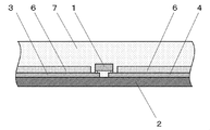
- FIG. 1 and 2 are sectional views of an optical semiconductor device (LED) which is an example of the electric / electronic component of the present invention.
- FIG. 1 is a sectional view of a chip-on-board (COB) type optical semiconductor device which is an example of the optical semiconductor device of the present invention.
- COB chip-on-board
- an optical semiconductor element 1 is mounted on a COB substrate 2 by die bonding, and the optical semiconductor element 1 and circuits 3 and 4 are electrically connected by a bonding wire 5.
- a light reflecting material 6 is formed around the optical semiconductor element 1 on the substrate 2 so as to efficiently reflect light emitted from the optical semiconductor element 1.
- FIG. 2 shows a sectional view of another chip-on-board (COB) type optical semiconductor device which is an example of the optical semiconductor device of the present invention.
- COB chip-on-board
- the optical semiconductor element 1 is electrically connected to the circuits 3 and 4 on the COB substrate 2 by bonding pads.
- a light reflecting material 6 is formed around the optical semiconductor element 1 on the substrate 2 so as to efficiently reflect light emitted from the optical semiconductor element 1.
- the substrate 2 may be a metal substrate such as aluminum or copper, and the circuits 3 and 4 are formed on the surface of the metal substrate via an insulating layer (not shown). Is formed.
- a non-metallic substrate is used as the substrate 2, it is not necessary to form an insulating layer.
- Such non-metallic substrates include glass epoxy substrates, polybutylene terephthalate (PBT) substrates, polyimide substrates, polyester substrates, aluminum nitride substrates, boron nitride substrates, silicon nitride substrates, alumina ceramic substrates, glass substrates, flexible glass substrates. Is illustrated.
- a hybrid substrate made of an aluminum substrate or a copper substrate having an insulating resin layer, a printed wiring silicon substrate, a silicon carbide substrate, or a sapphire substrate can be used as the substrate 2.
- the circuits 3 and 4 are made of at least one metal selected from the group consisting of silver, copper, and aluminum having high electrical conductivity, or an alloy containing at least one selected from the group consisting of silver, copper, and aluminum. Used.
- a primer layer (not shown) formed of the primer composition is formed on the surfaces of the circuits 3 and 4.
- a light reflecting material 6 is formed on the circuits 3 and 4 through the primer layer so as to expose a portion on which the optical semiconductor element 1 is mounted on the substrate 2.
- the optical semiconductor element 1 and the light reflecting material 6 are sealed with the sealing material 7, but only the optical semiconductor element 1 may be sealed with the sealing material 7 in a dome shape.
- FIG. 1 and FIG. 2 only one optical semiconductor element 1 is shown on the substrate 2, but a plurality of optical semiconductor elements 1 may be mounted on the substrate 2.
- the viscosity is a value at 25 ° C.
- Me, Ph, and Vi represent a methyl group, a phenyl group, and a vinyl group, respectively.
- the softening point of the organosiloxane block copolymer and the adhesion performance by the primer composition were evaluated as follows.
- a mixture of methyltriacetoxysilane and ethyltriacetoxysilane in a mass ratio of 1: 1 to a solution of 55.0 g of methylphenylpolysiloxane blocked with silanol groups at both ends of the molecular chain (polymerization degree 140) and 29.62 g of toluene 1.21 g was added to prepare a toluene solution of methylphenylpolysiloxane blocked with diacetoxy groups at both ends of the molecular chain (polymerization degree 140).
- Example 1 5 g of a solution of the organosiloxane block copolymer prepared in Reference Example 1 in toluene (solid concentration: 10% by mass), 1.0005 g of 1,8-diazabicyclo [5,4,0] -undec-7-ene (DBU), and toluene A primer composition was prepared by uniformly mixing 5 g. Next, this primer composition was uniformly coated on a glass plate so that the coating amount was 50 g / m 2 and dried at 100 ° C. for 30 minutes. The primer layer on the glass plate was slightly mottled and not uniform, but there was no surface tack. Next, the curable silicone composition prepared in Reference Example 3 was applied to the primer layer side of the glass plate to produce a die shear test piece. The die shear strength was measured and the results are shown in Table 1.
- Example 2 Toluene solution of organosiloxane block copolymer prepared in Reference Example 1 (solid content concentration: 10% by mass) 2.5 g, 1,8-diazabicyclo [5,4,0] -undec-7-ene (DBU) 0.0025 g, And a primer composition was prepared by uniformly mixing 7.5 g of toluene. Next, this primer composition was uniformly coated on a glass plate so that the coating amount was 50 g / m 2 and dried at 100 ° C. for 30 minutes. The primer layer on the glass plate was slightly mottled and not uniform, but there was no surface tack. Next, the curable silicone composition prepared in Reference Example 3 was applied to the primer layer side of the glass plate to produce a die shear test piece. The die shear strength was measured and the results are shown in Table 1.
- Example 3 1.0 g of a toluene solution of the organosiloxane block copolymer prepared in Reference Example 1 (solid content concentration: 10% by mass), 1.0001 g of 1,8-diazabicyclo [5,4,0] -undec-7-ene (DBU), A primer composition was prepared by uniformly mixing 9 g of toluene and 9 g of toluene. Next, this primer composition was uniformly coated on a glass plate so that the coating amount was 50 g / m 2 and dried at 100 ° C. for 30 minutes. The primer layer on the glass plate was uniform and had no surface tack. Next, the curable silicone composition prepared in Reference Example 3 was applied to the primer layer side of the glass plate to produce a die shear test piece. The die shear strength was measured and the results are shown in Table 1.
- Example 4 Toluene solution of organosiloxane block copolymer prepared in Reference Example 1 (solid content concentration: 10% by mass) 2.5 g, 1,8-diazabicyclo [5,4,0] -undec-7-ene (DBU) 0.0025 g, A primer composition was prepared by uniformly mixing 2.5 g of toluene and 5.0 g of n-heptane. Next, this primer composition was uniformly coated on a glass plate so that the coating amount was 50 g / m 2 and dried at 100 ° C. for 30 minutes. The primer layer on the glass plate was uniform and had no surface tack. Next, the curable silicone composition prepared in Reference Example 3 was applied to the primer layer side of the glass plate to produce a die shear test piece. The die shear strength was measured and the results are shown in Table 1.
- the primer composition of the present invention improves the adhesiveness of the silicone cured product to a base material such as an optical semiconductor element, a packaging material, and a substrate, and can suppress the peeling and cracking of the silicone cured product due to heat cycle, It is suitable as a primer composition in the production of an LED device having a large calorific value, such as a high-brightness and high-power LED.
Landscapes
- Chemical & Material Sciences (AREA)
- Organic Chemistry (AREA)
- Life Sciences & Earth Sciences (AREA)
- Engineering & Computer Science (AREA)
- Materials Engineering (AREA)
- Wood Science & Technology (AREA)
- Chemical Kinetics & Catalysis (AREA)
- Health & Medical Sciences (AREA)
- Medicinal Chemistry (AREA)
- Polymers & Plastics (AREA)
- Paints Or Removers (AREA)
- Adhesives Or Adhesive Processes (AREA)
- Led Device Packages (AREA)
- Silicon Polymers (AREA)
Abstract
Description
(A)平均単位式:
(R1 2SiO2/2)a(R2SiO3/2)b
(式中、R1およびR2は、それぞれ独立して、炭素数1~12のアルキル基、炭素数6~20のアリール基、または炭素数7~20のアラルキル基であり、aは0.40~0.90の数、bは0.10~0.60の数であり、かつ、a+b=1.00である。)
で表され、式:
[R2SiO3/2]
(式中、R2は前記と同じである。)
で表されるレジン状シロキサンブロックが、式:
-(R1 2SiO2/2)n-
(式中、R1は前記と同じであり、nは10~400の数である。)
で表される直鎖状シロキサンブロックにより連結され、ケイ素原子結合水酸基またはケイ素原子結合アルコキシ基を0.5~35.0モル%含有する、25℃において固体状であり、軟化点が200℃以下であるオルガノシロキサンブロックコポリマー、
(B)硬化触媒(本組成物の硬化を促進する量)、および
(C)任意量の有機溶媒
から少なくともなる。
(A)成分のオルガノシロキサンブロックコポリマーは、平均単位式:
(R1 2SiO2/2)a(R2SiO3/2)b
で表される。
[R2SiO3/2]
で表されるレジン状シロキサンブロックが、式:
-(R1 2SiO2/2)n-
で表される直鎖状シロキサンブロックにより連結されている。
[R2SiO3/2]
で表されるレジン状シロキサンブロックにおいて、式中、R2は炭素数1~12のアルキル基、炭素数6~20のアリール基、または炭素数7~20のアラルキル基であり、前記と同様の基が例示される。また、このレジン状シロキサンブロックの重量平均分子量は限定されないが、好ましくは、少なくとも500である。これは、このレジン状シロキサンブロックが、少なくとも3個以上の式:R2SiO3/2で表されるトリシロキサン単位からなることを意味する。なお、この重量平均分子量は、原料であるレジン状シロキサンに由来するものであり、原料のレジン状シロキサンをゲル透過クロマトグラフィー(GPC)により測定することができる。
-(R1 2SiO2/2)n-
で表される直鎖状シロキサンブロックにおいて、式中、R1は、それぞれ独立して、炭素数1~12のアルキル基、炭素数6~20のアリール基、または炭素数7~20のアラルキル基であり、前記と同様の基が例示される。
[R2SiO3/2]
で表されるレジン状シロキサンブロックが、式:
-(R1 2SiO2/2)n-
で表される直鎖状シロキサンブロックにより連結され、前記レジン状シロキサンブロックが、更に凝集して、「硬い」ポリマーブロックからなる「ナノドメイン」を形成しているので、このオルガノシロキサンブロックコポリマーを室温で固体状となる。一方、相分離した直鎖状シロキサンブロックは「軟らかい」ポリマーブロックを形成しており、この相分離された「軟らかい」ポリマーブロックと「硬い」ポリマーブロックは、異なるガラス転移温度(Tg)、具体的には、25℃未満、0℃未満、あるいは-20℃未満といったより低いTgを有する「軟らかい」ポリマーブロックと、30℃超、40℃超、あるいは50℃超といった、より高いTgを有する「硬い」ポリマーブロックからなる。その結果、光半導体素子、パッケージ材料、基板等の基材を本組成物により形成したプライマー層を介して接着したシリコーン硬化物がヒートサイクル等を受けても、プライマー層により応力を緩和して前記シリコーン硬化物のピールやクラックを抑制することができる。
次に、本発明の接着方法を詳細に説明する。
本発明の接着方法では、はじめに上記のプライマー組成物を基材上に塗布する。
(I)一分子中に少なくとも2個のアルケニル基を有するオルガノポリシロキサン、
(II)一分子中に少なくとも2個のケイ素原子結合水素原子を有するオルガノポリシロキサン、および
(III)ヒドロシリル化反応用触媒
から少なくともなる。
次に、本発明の電気・電子部品を詳細に説明する。
本発明の電気・電子部品は、電気・電子用基材、該基材上のプライマー層、および該プライマー層上のシリコーン硬化物からなる電気・電子部品であって、上記のプライマー組成物により形成されてなることを特徴とする。この電気・電子部品としては、光半導体装置(LED)が例示される。
オルガノシロキサンブロックコポリマーをφ14mm×22mmの円柱状のタブレット状に成型し、このタブレットを25℃~100℃に設定したホットプレート上に置き、100グラム重の荷重で上から10秒間押し続け、荷重を取り除いた後、該タブレットの変形量を測定した。高さ方向の変形量が1mm以上となった温度を軟化点とした。
25mm×75mmのガラス基板上に硬化性シリコーン組成物をディスペンサーにより約100mgずつ5ヶ所に塗布した。次に、この組成物に厚さ1mmの6mm角のアルミニウム製チップを被せ、1kgの板により圧着した状態で、150℃で2時間加熱して硬化させた後、室温に冷却して、ダイシェア試験片を作製した。この試験片のダイシェア強度をダイシェア強度測定装置(西進商事株式会社製のボンドテスターSS-100KP)により測定し、その平均値を求めた。
温度計、テフロン(登録商標)製の撹拌パドル、および水冷凝縮器を取り付けたDean Stark装置を装着した500mLの四つ口丸底フラスコに、平均単位式:PhSiO3/2で示され、重量平均分子量が1,300であるオルガノポリシロキサンレジン 45.0gとトルエン 70.38gを投入し、窒素雰囲気下、攪拌しながら加熱した。反応混合物をトルエン還流させながら30分間加熱した後、反応混合物を108℃に冷却した。
(PhMeSiO2/2)0.55(PhSiO3/2)0.45
で表され、式:
(PhSiO3/2)
で表されるフェニルシロキサンレジンブロックが式:
-(PhMeSiO2/2)140-
で表されるメチルフェニルシロキサンブロックにより連結され、16モル%のケイ素原子結合水酸基を有し、軟化点が55℃であるオルガノシロキサンブロックコポリマーであることがわかった。
n-ヘプタン 100質量部に、アリルトリメトキシシラン 10質量部を加えて混合した後、テトラ(n-ブチル)チタネート 2質量部を加えて均一に混合した後、塩化白金酸と1,3-ジビニルテトラメチルジシロキサンとの錯体 0.1質量部を加えて均一に混合したプライマー組成物を調製した。
式:
-(MeViSiO)20-
で表される直鎖状メチルビニルシロキサンブロックを有し、分子鎖両末端が水酸基で封鎖されたメチルビニルポリシロキサン 4.4質量部、式:
Me2ViSiO(Me2SiO)160SiMe2Vi
で表される分子鎖両末端ジメチルビニルシロキシ基封鎖ジメチルポリシロキサン 4.1質量部、平均一次粒子径0.2μmの酸化チタン(堺化学工業製のSX-3103) 51.8質量部、平均粒子径15μmの球状シリカ(新日鉄マテリアルズ マイクロン社製のHS-202) 30質量部、および粘度24mPa・sである、式:
Me2ViSiO(Me2SiO)29Si(OMe)3
で表される分子鎖片末端がジメチルビニルシロキシ基で封鎖され、他の分子鎖片末端がトリメトキシシロキシ基で封鎖されたジメチルポリシロキサン 4質量部をロスミキサーに投入し、室温で混合した後、減圧下、150℃に加熱しながら混練して、シリコーンベースを調製した。
-(MeHSiO)50-
で表される直鎖状メチルハイドロジェンシロキサンブロックを有し、分子鎖両末端がトリメチルシロキシ基で封鎖されたメチルハイドロジェンポリシロキサン 4.7質量部(シリコーンベース中のメチルビニルポリシロキサンと分子鎖両末端ジメチルビニルシロキシ基封鎖ジメチルポリシロキサン中のビニル基の合計1モルに対して、本成分中のケイ素原子結合水素原子が1.5モルとなる量)、粘度20mPa・sの分子鎖両末端水酸基封鎖ジメチルシロキサン・メチルビニルシロキサン共重合オリゴマーと3-グリシドキシプロピルトリメトキシシランとの質量比1:2の縮合反応物 1質量部、および1-エチニル-1-シクロヘキサノール(本組成物に対して、質量単位で200ppmとなる量)を混合した後、白金の1,3-ジビニル-1,1,3,3-テトラメチルジシロキサンの1,3-ジビニル-1,1,3,3-テトラメチルジシロキサン溶液(本組成物に対して、白金原子が質量単位で3.5ppmとなる量)を混合して、硬化性シリコーン組成物を調製した。
参考例1で調製したオルガノシロキサンブロックコポリマーのトルエン溶液(固形分濃度10質量%) 5g、1,8-ジアザビシクロ[5,4,0]-ウンデカ-7-エン(DBU) 0.0005g、およびトルエン 5gを均一に混合してプライマー組成物を調製した。次に、このプライマー組成物をガラス板に塗布量が50g/m2となる様に均一に塗布し、100℃で30分間乾燥させた。ガラス板上のプライマー層は若干まだらで均一ではなかったが、表面タックは全くなかった。次に、ガラス板のプライマー層側に、参考例3で調製した硬化性シリコーン組成物を塗布し、ダイシェア試験片を作製した。ダイシェア強度を測定し、その結果を表1に示した。
参考例1で調製したオルガノシロキサンブロックコポリマーのトルエン溶液(固形分濃度10質量%) 2.5g、1,8-ジアザビシクロ[5,4,0]-ウンデカ-7-エン(DBU) 0.00025g、およびトルエン 7.5gを均一に混合してプライマー組成物を調製した。次に、このプライマー組成物をガラス板上に塗布量が50g/m2となる様に均一に塗布し、100℃で30分間乾燥させた。ガラス板上のプライマー層は若干まだらで、均一ではなかったが、表面タックは全くなかった。次に、ガラス板のプライマー層側に、参考例3で調製した硬化性シリコーン組成物を塗布し、ダイシェア試験片を作製した。ダイシェア強度を測定し、その結果を表1に示した。
参考例1で調製したオルガノシロキサンブロックコポリマーのトルエン溶液(固形分濃度10質量%) 1.0g、1,8-ジアザビシクロ[5,4,0]-ウンデカ-7-エン(DBU) 0.0001g、およびトルエン 9gを均一に混合してプライマー組成物を調製した。次に、このプライマー組成物をガラス板に塗布量が50g/m2となる様に均一に塗布し、100℃で30分間乾燥させた。ガラス板上のプライマー層は均一であり、表面タックは全くなかった。次に、ガラス板のプライマー層側に、参考例3で調製した硬化性シリコーン組成物を塗布し、ダイシェア試験片を作製した。ダイシェア強度を測定し、その結果を表1に示した。
参考例1で調製したオルガノシロキサンブロックコポリマーのトルエン溶液(固形分濃度10質量%) 2.5g、1,8-ジアザビシクロ[5,4,0]-ウンデカ-7-エン(DBU) 0.00025g、トルエン 2.5g、およびn-ヘプタン 5.0gを均一に混合してプライマー組成物を調製した。次に、このプライマー組成物をガラス板に塗布量が50g/m2となる様に均一に塗布し、100℃で30分間乾燥させた。ガラス板上のプライマー層は均一であり、表面タックは全くなかった。次に、ガラス板のプライマー層側に、参考例3で調製した硬化性シリコーン組成物を塗布し、ダイシェア試験片を作製した。ダイシェア強度を測定し、その結果を表1に示した。
プライマー処理していないガラス板に、参考例3で調製した硬化性シリコーン組成物を塗布し、ダイシェア試験片を作製した。ダイシェア強度を測定し、その結果を表1に示した。
参考例2で調製したプライマー組成物をガラス板に塗布量が50g/m2となる様に均一に塗布し、100℃で30分間乾燥させた。ガラス板上のプライマー層は均一であった。次に、ガラス板のプライマー層側に、参考例3で調製した硬化性シリコーン組成物を塗布し、ダイシェア試験片を作製した。ダイシェア強度を測定し、その結果を表1に示した。

2 基板
3 回路
4 回路
5 ボンディングワイヤ
6 光反射材
7 硬化性シリコーン組成物の硬化物
Claims (12)
- (A)平均単位式:
(R1 2SiO2/2)a(R2SiO3/2)b
(式中、R1およびR2は、それぞれ独立して、炭素数1~12のアルキル基、炭素数6~20のアリール基、または炭素数7~20のアラルキル基であり、aは0.40~0.90の数、bは0.10~0.60の数であり、かつ、a+b=1.00である。)
で表され、式:
[R2SiO3/2]
(式中、R2は前記と同じである。)
で表されるレジン状シロキサンブロックが、式:
-(R1 2SiO2/2)n-
(式中、R1は前記と同じであり、nは10~400の数である。)
で表される直鎖状シロキサンブロックにより連結され、ケイ素原子結合水酸基またはケイ素原子結合アルコキシ基を0.5~35.0モル%含有する、25℃において固体状であり、軟化点が200℃以下であるオルガノシロキサンブロックコポリマー、
(B)硬化触媒(本組成物の硬化を促進する量)、および
(C)任意量の有機溶媒
から少なくともなるプライマー組成物。 - (A)成分中のR1がアルキル基および/またはアリール基である、請求項1に記載のプライマー組成物。
- (A)成分中のR2がアリール基である、請求項1または2に記載のプライマー組成物。
- (B)成分が縮合反応触媒である、請求項1に記載のプライマー組成物。
- (C)成分が、芳香族炭化水素系溶媒、または芳香族炭化水素系溶媒と脂肪族炭化水素系溶媒の混合溶媒である、請求項1に記載のプライマー組成物。
- 基材に硬化性シリコーン組成物を接着するための、請求項1乃至5のいずれか1項に記載のプライマー組成物。
- 硬化性シリコーン組成物がヒドロリル化反応硬化性シリコーン組成物である、請求項6に記載のプライマー組成物。
- 基材が電気・電子部品である、請求項6に記載のプライマー組成物。
- 請求項1~8のいずれか1項に記載のプライマー組成物を基材上に塗布し、有機溶媒を除去した後、得られたプライマー層上に硬化性シリコーン組成物を塗布して硬化することを特徴とする接着方法。
- 硬化性シリコーン組成物をプライマー層の硬化と同時に行うことを特徴とする、請求項9に記載の接着方法。
- 電気・電子用基材、該基材上のプライマー層、および該プライマー層上のシリコーン硬化物からなる電気・電子部品であって、前記プライマー層が請求項1~8のいずれか1項に記載のプライマー組成物により形成されてなる電気・電子部品。
- 電気・電子部品が光半導体装置である、請求項11に記載の電気・電子部品。
Priority Applications (5)
| Application Number | Priority Date | Filing Date | Title |
|---|---|---|---|
| KR1020177025928A KR20170124558A (ko) | 2015-02-26 | 2016-02-23 | 프라이머 조성물, 접착 방법 및 전기·전자 부품 |
| CN201680015993.7A CN107429115A (zh) | 2015-02-26 | 2016-02-23 | 底漆组合物、粘附方法和电/电子部件 |
| JP2017501937A JP6666896B2 (ja) | 2015-02-26 | 2016-02-23 | プライマー組成物、接着方法、および電気・電子部品 |
| EP16754994.8A EP3275955B1 (en) | 2015-02-26 | 2016-02-23 | Electric/electronic part and bonding method |
| US15/553,407 US10479910B2 (en) | 2015-02-26 | 2016-02-23 | Primer composition, adhering method, and electric/electronic part |
Applications Claiming Priority (2)
| Application Number | Priority Date | Filing Date | Title |
|---|---|---|---|
| JP2015-037452 | 2015-02-26 | ||
| JP2015037452 | 2015-02-26 |
Publications (1)
| Publication Number | Publication Date |
|---|---|
| WO2016136244A1 true WO2016136244A1 (ja) | 2016-09-01 |
Family
ID=56788337
Family Applications (1)
| Application Number | Title | Priority Date | Filing Date |
|---|---|---|---|
| PCT/JP2016/000960 Ceased WO2016136244A1 (ja) | 2015-02-26 | 2016-02-23 | プライマー組成物、接着方法、および電気・電子部品 |
Country Status (7)
| Country | Link |
|---|---|
| US (1) | US10479910B2 (ja) |
| EP (1) | EP3275955B1 (ja) |
| JP (1) | JP6666896B2 (ja) |
| KR (1) | KR20170124558A (ja) |
| CN (1) | CN107429115A (ja) |
| TW (1) | TWI682009B (ja) |
| WO (1) | WO2016136244A1 (ja) |
Cited By (2)
| Publication number | Priority date | Publication date | Assignee | Title |
|---|---|---|---|---|
| CN113717637A (zh) * | 2021-09-07 | 2021-11-30 | 河南三棵树新材料科技有限公司 | 一种耐高温防腐涂料及其制备方法 |
| WO2025197877A1 (ja) * | 2024-03-19 | 2025-09-25 | 日産化学株式会社 | プライマー皮膜形成用組成物、積層体、積層体の製造方法、及び加工された半導体基板又は電子デバイス基板の製造方法 |
Families Citing this family (7)
| Publication number | Priority date | Publication date | Assignee | Title |
|---|---|---|---|---|
| CA2895256C (en) | 2013-01-09 | 2021-06-01 | BASF Agro B.V. | Process for the preparation of substituted oxiranes and triazoles |
| UA120628C2 (uk) | 2014-11-07 | 2020-01-10 | Басф Се | Пестицидні суміші |
| JP6447557B2 (ja) * | 2016-03-24 | 2019-01-09 | 日亜化学工業株式会社 | 発光装置の製造方法 |
| MX2018015764A (es) | 2016-06-15 | 2019-08-29 | Basf Agro Bv | Proceso para la epoxidacion de un alqueno tetrasustituido. |
| US20240262970A1 (en) * | 2019-04-29 | 2024-08-08 | Dow Silicones Corporation | Method for improving the adhesion of silicone elastomers to pre-cured silicone elastomeric substrates, and primer composition for silicone rubber compositions and elastomeric materials |
| WO2020223182A1 (en) * | 2019-04-29 | 2020-11-05 | Dow Silicones Corporation | Primer for silicone rubber compositions and elastomeric materials |
| CN115681919A (zh) * | 2022-11-01 | 2023-02-03 | 光之能(厦门)照明有限公司 | 一种微流管基板 |
Citations (3)
| Publication number | Priority date | Publication date | Assignee | Title |
|---|---|---|---|---|
| JP2004075970A (ja) * | 2002-06-18 | 2004-03-11 | Shin Etsu Chem Co Ltd | ハードコート剤及びハードコート膜が形成された物品 |
| JP2014510802A (ja) * | 2011-02-04 | 2014-05-01 | ダウ コーニング コーポレーション | 硬化性オルガノシロキサンブロックコポリマーエマルション |
| WO2014129347A1 (ja) * | 2013-02-20 | 2014-08-28 | 横浜ゴム株式会社 | 硬化性樹脂組成物 |
Family Cites Families (11)
| Publication number | Priority date | Publication date | Assignee | Title |
|---|---|---|---|---|
| BE759621A (fr) * | 1969-12-01 | 1971-06-01 | Dow Corning | Copolymeres sequences d'organosiloxanes non corrosifs, vulcanisables a la temperature ambiante |
| JP3527369B2 (ja) | 1996-09-04 | 2004-05-17 | 東レ・ダウコーニング・シリコーン株式会社 | 電気部品およびその製造方法 |
| JP2004339450A (ja) | 2003-05-19 | 2004-12-02 | Kanegafuchi Chem Ind Co Ltd | プライマー組成物、及び該プライマーを用いた発光ダイオード |
| JP4623282B2 (ja) | 2005-03-10 | 2011-02-02 | 信越化学工業株式会社 | 半導体装置の製造方法 |
| JP4777802B2 (ja) | 2006-03-17 | 2011-09-21 | 信越化学工業株式会社 | 耐光性プライマー組成物、該プライマー組成物を用いる発光半導体装置の製造方法、及び該方法により得られる発光半導体装置 |
| EP2619246B1 (en) * | 2010-09-22 | 2014-07-16 | Dow Corning Corporation | Resin-linear organosiloxane block copolymers |
| US9045668B2 (en) * | 2010-09-22 | 2015-06-02 | Dow Corning Corporation | Organosiloxane block copolymer |
| WO2013090691A1 (en) | 2011-12-14 | 2013-06-20 | Dow Corning Corporation | Curable compositions of resin-linear organosiloxane block copolymers |
| US9175140B2 (en) | 2012-03-21 | 2015-11-03 | Dow Corning Corporation | Compositions of resin-linear organosiloxane block copolymers |
| KR20150132380A (ko) * | 2013-03-15 | 2015-11-25 | 다우 코닝 코포레이션 | 수지-선형 유기실록산 블록 공중합체의 조성물 |
| WO2014150841A2 (en) | 2013-03-15 | 2014-09-25 | Dow Corning Corporation | Powdered resin linear organopolysiloxane compositions |
-
2016
- 2016-02-23 WO PCT/JP2016/000960 patent/WO2016136244A1/ja not_active Ceased
- 2016-02-23 CN CN201680015993.7A patent/CN107429115A/zh active Pending
- 2016-02-23 US US15/553,407 patent/US10479910B2/en not_active Expired - Fee Related
- 2016-02-23 EP EP16754994.8A patent/EP3275955B1/en not_active Not-in-force
- 2016-02-23 KR KR1020177025928A patent/KR20170124558A/ko not_active Abandoned
- 2016-02-23 JP JP2017501937A patent/JP6666896B2/ja not_active Expired - Fee Related
- 2016-02-24 TW TW105105532A patent/TWI682009B/zh not_active IP Right Cessation
Patent Citations (3)
| Publication number | Priority date | Publication date | Assignee | Title |
|---|---|---|---|---|
| JP2004075970A (ja) * | 2002-06-18 | 2004-03-11 | Shin Etsu Chem Co Ltd | ハードコート剤及びハードコート膜が形成された物品 |
| JP2014510802A (ja) * | 2011-02-04 | 2014-05-01 | ダウ コーニング コーポレーション | 硬化性オルガノシロキサンブロックコポリマーエマルション |
| WO2014129347A1 (ja) * | 2013-02-20 | 2014-08-28 | 横浜ゴム株式会社 | 硬化性樹脂組成物 |
Non-Patent Citations (1)
| Title |
|---|
| See also references of EP3275955A4 * |
Cited By (3)
| Publication number | Priority date | Publication date | Assignee | Title |
|---|---|---|---|---|
| CN113717637A (zh) * | 2021-09-07 | 2021-11-30 | 河南三棵树新材料科技有限公司 | 一种耐高温防腐涂料及其制备方法 |
| CN113717637B (zh) * | 2021-09-07 | 2022-08-02 | 河南三棵树新材料科技有限公司 | 一种耐高温防腐涂料及其制备方法 |
| WO2025197877A1 (ja) * | 2024-03-19 | 2025-09-25 | 日産化学株式会社 | プライマー皮膜形成用組成物、積層体、積層体の製造方法、及び加工された半導体基板又は電子デバイス基板の製造方法 |
Also Published As
| Publication number | Publication date |
|---|---|
| TWI682009B (zh) | 2020-01-11 |
| EP3275955A1 (en) | 2018-01-31 |
| US10479910B2 (en) | 2019-11-19 |
| US20180105720A1 (en) | 2018-04-19 |
| TW201638256A (zh) | 2016-11-01 |
| JPWO2016136244A1 (ja) | 2017-12-07 |
| EP3275955A4 (en) | 2018-08-01 |
| JP6666896B2 (ja) | 2020-03-18 |
| CN107429115A (zh) | 2017-12-01 |
| EP3275955B1 (en) | 2020-05-27 |
| KR20170124558A (ko) | 2017-11-10 |
Similar Documents
| Publication | Publication Date | Title |
|---|---|---|
| JP6666896B2 (ja) | プライマー組成物、接着方法、および電気・電子部品 | |
| CN106661329B (zh) | 固化性有机硅组合物、其固化物以及光半导体装置 | |
| TWI831733B (zh) | 固化性粒狀聚矽氧組合物、由其構成之半導體用構件及其成型方法 | |
| TWI709615B (zh) | 硬化性粒狀聚矽氧組合物及其製造方法 | |
| KR101566556B1 (ko) | 열경화성 실리콘 수지 조성물, 실리콘 수지, 실리콘 수지 시트 및 그의 용도 | |
| JP5469874B2 (ja) | 硬化性オルガノポリシロキサン組成物、光半導体素子封止剤および光半導体装置 | |
| CN103582679B (zh) | 可交联有机硅组合物及其交联产物 | |
| JP6355210B2 (ja) | 半導体装置および半導体素子封止用硬化性シリコーン組成物 | |
| US9068049B2 (en) | Curable silicone composition and cured product thereof | |
| JP6552488B2 (ja) | オルガノシロキサン、硬化性シリコーン組成物、および半導体装置 | |
| TW201817816A (zh) | 固化性粒狀聚矽氧組合物、由其構成之半導體用構件及其成型方法 | |
| JP2012507582A (ja) | 硬化性オルガノポリシロキサン組成物、光半導体素子封止剤および光半導体装置 | |
| TWI583741B (zh) | 可固化組成物 | |
| JP2014084417A (ja) | オルガノポリシロキサン、硬化性シリコーン組成物、その硬化物、および光半導体装置 | |
| CN114144477B (zh) | 可固化有机聚硅氧烷组合物、固化产物和电气/电子设备 | |
| KR20190050999A (ko) | 경화성 수지 조성물, 그의 경화물 및 반도체 장치 | |
| CN105492541A (zh) | 加成固化型有机硅树脂组合物、加成固化型有机硅树脂固化物和光半导体元件封装体 | |
| CN104508046B (zh) | 可固化组合物 | |
| CN119177111A (zh) | 可固化硅酮组合物 | |
| TW202532534A (zh) | 熱熔性硬化性矽酮組成物、密封材料、熱熔性接著劑以及光半導體裝置 | |
| WO2015083446A1 (ja) | 付加硬化型シリコーン樹脂組成物、付加硬化型シリコーン樹脂硬化物、及び、光半導体素子封止体 |
Legal Events
| Date | Code | Title | Description |
|---|---|---|---|
| 121 | Ep: the epo has been informed by wipo that ep was designated in this application |
Ref document number: 16754994 Country of ref document: EP Kind code of ref document: A1 |
|
| ENP | Entry into the national phase |
Ref document number: 2017501937 Country of ref document: JP Kind code of ref document: A |
|
| REEP | Request for entry into the european phase |
Ref document number: 2016754994 Country of ref document: EP |
|
| WWE | Wipo information: entry into national phase |
Ref document number: 15553407 Country of ref document: US |
|
| NENP | Non-entry into the national phase |
Ref country code: DE |
|
| ENP | Entry into the national phase |
Ref document number: 20177025928 Country of ref document: KR Kind code of ref document: A |