WO2016140044A1 - フォトマスクブランク、フォトマスクの製造方法及びマスクパターン形成方法 - Google Patents
フォトマスクブランク、フォトマスクの製造方法及びマスクパターン形成方法 Download PDFInfo
- Publication number
- WO2016140044A1 WO2016140044A1 PCT/JP2016/054225 JP2016054225W WO2016140044A1 WO 2016140044 A1 WO2016140044 A1 WO 2016140044A1 JP 2016054225 W JP2016054225 W JP 2016054225W WO 2016140044 A1 WO2016140044 A1 WO 2016140044A1
- Authority
- WO
- WIPO (PCT)
- Prior art keywords
- film
- oxygen
- photomask
- gas
- dry etching
- Prior art date
- Legal status (The legal status is an assumption and is not a legal conclusion. Google has not performed a legal analysis and makes no representation as to the accuracy of the status listed.)
- Ceased
Links
Images






Classifications
-
- G—PHYSICS
- G03—PHOTOGRAPHY; CINEMATOGRAPHY; ANALOGOUS TECHNIQUES USING WAVES OTHER THAN OPTICAL WAVES; ELECTROGRAPHY; HOLOGRAPHY
- G03F—PHOTOMECHANICAL PRODUCTION OF TEXTURED OR PATTERNED SURFACES, e.g. FOR PRINTING, FOR PROCESSING OF SEMICONDUCTOR DEVICES; MATERIALS THEREFOR; ORIGINALS THEREFOR; APPARATUS SPECIALLY ADAPTED THEREFOR
- G03F1/00—Originals for photomechanical production of textured or patterned surfaces, e.g., masks, photo-masks, reticles; Mask blanks or pellicles therefor; Containers specially adapted therefor; Preparation thereof
- G03F1/26—Phase shift masks [PSM]; PSM blanks; Preparation thereof
- G03F1/32—Attenuating PSM [att-PSM], e.g. halftone PSM or PSM having semi-transparent phase shift portion; Preparation thereof
-
- G—PHYSICS
- G03—PHOTOGRAPHY; CINEMATOGRAPHY; ANALOGOUS TECHNIQUES USING WAVES OTHER THAN OPTICAL WAVES; ELECTROGRAPHY; HOLOGRAPHY
- G03F—PHOTOMECHANICAL PRODUCTION OF TEXTURED OR PATTERNED SURFACES, e.g. FOR PRINTING, FOR PROCESSING OF SEMICONDUCTOR DEVICES; MATERIALS THEREFOR; ORIGINALS THEREFOR; APPARATUS SPECIALLY ADAPTED THEREFOR
- G03F1/00—Originals for photomechanical production of textured or patterned surfaces, e.g., masks, photo-masks, reticles; Mask blanks or pellicles therefor; Containers specially adapted therefor; Preparation thereof
- G03F1/38—Masks having auxiliary features, e.g. special coatings or marks for alignment or testing; Preparation thereof
Definitions
- the present invention relates to a photomask blank which is a material for manufacturing a photomask used when manufacturing a semiconductor integrated circuit or the like, a photomask manufacturing method, and a mask pattern forming method.
- circuit pattern miniaturization has become more and more necessary, especially due to the high integration of large-scale integrated circuits, and the wiring patterns that make up circuits have become thinner and the layers that make up cells.
- the photomask pattern In order to form a photomask pattern with higher accuracy on the photomask substrate, it is first necessary to form a highly accurate resist pattern on the photomask blank. Since optical lithography when processing an actual semiconductor substrate performs a reduction projection, the photomask pattern is about four times larger than the actually required pattern size, but this does not mean that the accuracy is reduced. High accuracy is required for the mask.
- the circuit pattern to be drawn is a size that is considerably smaller than the wavelength of the light to be used. If a photomask pattern in which the shape of the circuit is four times as it is is used, Due to the influence of light interference or the like that occurs when performing this photolithography, the shape according to the photomask pattern is not transferred to the resist film. Therefore, in order to reduce these effects, the photomask pattern may need to be processed into a more complicated shape than an actual circuit pattern (a shape to which so-called OPC: Optical Proximity Correction (optical proximity effect correction) or the like is applied). .
- OPC Optical Proximity Correction
- Lithographic performance may be expressed with a limit resolution, but this resolution limit is equivalent to or higher than the resolution limit required for optical lithography used in semiconductor processing processes using photomasks. Is required for the lithography technique in the photomask processing step.
- a photoresist film is usually formed on a photomask blank having a light-shielding film on a transparent substrate, a pattern is drawn with an electron beam, and a resist pattern is obtained through development. Then, using the obtained resist pattern as an etching mask, the light shielding film is etched to be processed into a light shielding film pattern.
- the film thickness of the photoresist film is the same as before the miniaturization. If processing is performed while maintaining the ratio of the film thickness to the pattern, the so-called aspect ratio increases, the pattern shape of the resist deteriorates, and pattern transfer cannot be performed properly, or in some cases the resist pattern falls down or peels off. It will cause. For this reason, it is necessary to make the resist film thinner with miniaturization.
- Patent Document 1 MoSi 2 It has been reported that a SiO 2 film is formed on a film, and this is used as an etching mask when a MoSi 2 film is dry-etched using a gas containing chlorine, and the SiO 2 film is used as an antireflection film. It can be said that it can function as well.
- Patent Document 2 Japanese Patent Application Laid-Open No. 7-49558 (Patent Document 2) describes that a chromium film is used as a light shielding film on a phase shift film, and an SiO 2 film is used as a hard mask on the chromium film. .
- silicon dioxide films such as SiO 2 films are generally processed by dry etching using a fluorine-based gas.
- dry etching using a fluorine-based gas has a problem that the etching rate is slow for silicon dioxide films. is there.
- it is effective from the viewpoint of the above-described etching rate to reduce the thickness of the hard mask film.
- the film is formed, islands grow in the initial stage of the film formation, and thus the film has a slight thickness distribution, that is, a thick part and a thin part in the plane.
- the film thickness of the photoresist film formed on the hard mask film also needs to be appropriate for the film thickness of the hard mask film.
- the resist pattern does not deteriorate on the hard mask film, and does not fall down or peel off. A method that can be stably maintained is required.
- the present invention has been made to solve the above-described problems, and includes a light shielding film for a photomask blank, an optical film such as an antireflection film, an etching mask film (hard mask film), a processing auxiliary film such as an etching stopper film, and the like.
- a fine resist pattern is formed from a photoresist film by improving adhesion between the film made of silicon and oxygen or a film made of silicon and oxygen and nitrogen and a photoresist film used as a hard mask for the film
- a photomask blank that maintains a stable pattern without degradation, falling, or peeling.
- to provide a manufacturing method and a mask pattern forming method of a photomask using an etching mask film and the photoresist film adhesion is improved beauty.
- the present inventors have assisted processing of photomask blank light shielding films, optical films such as antireflection films, etching mask films (hard mask films), etching stopper films, etc.
- Used as a film, etc. composed of a material that is etched by chlorine-oxygen dry etching with a mixed gas of chlorine gas and oxygen gas, such as a material containing chromium, and resistant to fluorine-based dry etching with a gas containing fluorine
- a film used as a hard mask for the formed film is composed of silicon and oxygen, or silicon and oxygen and nitrogen, and a material having a Si—Si bond.
- Adhesion is improved, and even if a fine resist pattern is formed from a photoresist film, the resist pattern is inferior.
- a fine mask pattern with good shape and dimensional accuracy can be formed in etching of a film under the resist pattern, which is stably maintained without causing collapse or peeling. It came.
- the present invention provides the following photomask blank, photomask manufacturing method, and mask pattern forming method.
- a membrane The material is formed in contact with the first film, and is made of a material that is made of silicon and oxygen, or silicon, oxygen, and nitrogen, and that is not substantially etched by the chlorine-oxygen dry etching that etches the first film. And a second film, and the second film is made of a material having a Si—Si bond.
- the photoresist film is formed in contact with the second film and has a film thickness of 150 nm or less, and the photoresist film is a chemically amplified resist film.
- Photomask blank [3] The photomask blank according to [1] or [2], wherein the second film contains oxygen at a ratio of 1 atomic% to 66 atomic%.
- a first material comprising a material that is etched on a transparent substrate by chlorine-oxygen dry etching using a mixed gas of chlorine gas and oxygen gas, and that is resistant to fluorine-based dry etching using a gas containing fluorine.
- Forming a film In the chlorine-oxygen-based dry etching, which is in contact with the first film, is composed of silicon and oxygen or silicon and oxygen and nitrogen, has a Si—Si bond, and etches the first film.
- Forming a second film composed of a material that is not etched; Forming a chemically amplified resist film having a thickness of 150 nm or less in contact with the second film; Forming a resist pattern by patterning the chemically amplified resist film; Using the resist pattern as an etching mask, patterning the second film by the fluorine-based dry etching to form a mask pattern of the second film, and using the mask pattern of the second film as an etching mask, A method of manufacturing a photomask, comprising: patterning the first film by the chlorine-oxygen-based dry etching to form a mask pattern of the first film.
- [8] Forming a phase shift film between the transparent substrate and the first film, and patterning the phase shift film by fluorine-based dry etching using the mask pattern of the first film as an etching mask And the manufacturing method of [7] characterized by including the process of forming the mask pattern of a phase shift film.
- a film formed on a transparent substrate of a photomask blank which is etched by chlorine oxygen dry etching using a mixed gas of chlorine gas and oxygen gas, and is resistant to fluorine dry etching by a gas containing fluorine.
- a method of forming a mask pattern comprising: patterning the first film by chlorine-oxygen dry etching to form a mask pattern of the first film.
- the adhesion of the photoresist film is improved, and even if a fine resist pattern is formed from the photoresist film, the resist pattern is maintained stably without causing deterioration, collapse, or peeling.
- good shape and dimensional accuracy can be obtained.
- a photomask having a highly accurate fine mask pattern can be provided.
- the photomask blank of the first aspect of the present invention includes a transparent substrate, a first film formed on the transparent substrate, and a second film formed in contact with the first film.
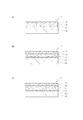
- FIG. 1A is a cross-sectional view showing an example of the photomask blank according to the first aspect of the present invention.
- This photomask blank 1 is formed on a transparent substrate 10 in contact with the transparent substrate 10. 1 film 11 and a second film 12 formed in contact with the first film 11.
- FIG. 1B is a cross-sectional view of an example of a photomask manufactured from the photomask blank shown in FIG.
- FIG. 1B shows a case where the second film is a film that functions as a part of the optical film.
- the mask pattern 11 a of the first film is formed on the transparent substrate 10 in the photomask 101.
- a mask pattern 12a of the second film is formed on the mask pattern 11a of the first film.
- FIG. 1C shows the case where the second film is a processing auxiliary film, and the mask pattern 11 a of the first film is formed on the transparent substrate 10 in the photomask 102.
- the transparent substrate 10 and the first film 11 are shown in contact with each other, but another film, for example, between the transparent substrate and the first film, for example,
- a phase shift film such as a halftone phase shift film, an optical film such as a light shielding film or an antireflection film, a processing auxiliary film such as an etching mask film (hard mask film), an etching stopper film, or the like may be formed.
- a phase shift film is formed between the transparent substrate and the first film, a phase shift film and a light shielding film are sequentially formed from the transparent substrate side, a phase shift film, Examples include an etching stopper film and a light shielding film formed in order.
- FIG. 2 (A) and FIG. 2 (B) are cross-sectional views showing other examples of the photomask blank according to the first aspect of the present invention.
- the photomask blank 1 of FIG. On top, the phase shift film 14 formed in contact with the transparent substrate 10, the first film 11 formed in contact with the phase shift film 14, and the second film formed in contact with the first film 11 12.
- the photomask blank 1 in FIG. 2B includes a phase shift film 14 formed on the transparent substrate 10 in contact with the transparent substrate 10, a light shielding film 15 formed in contact with the phase shift film 14, A first film 11 formed in contact with the light shielding film 15 and a second film 12 formed in contact with the first film 11 are provided.
- the photomask blank of the present invention may further have a photoresist film formed in contact with the second film.
- This case is the photomask blank of the second aspect.
- a photomask blank shown in FIG. FIG. 3A is a cross-sectional view showing an example of the photomask blank according to the second aspect of the present invention.
- This photomask blank 1 is formed on the transparent substrate 10 in contact with the transparent substrate 10.
- examples of the photomask manufactured from the photomask blank shown in FIG. 3A include the same ones as shown in FIGS. 1B and 1C.
- FIG. 3 (A) the transparent substrate 10 and the first film 11 formed in contact with each other are shown.
- another film similar to the photomask blank of the first aspect may be formed.
- membrane is mentioned.
- FIGS. 3B and 3C are cross-sectional views showing other examples of the photomask blank of the second aspect of the present invention.
- the photomask blank 1 of FIG. On top, the phase shift film 14 formed in contact with the transparent substrate 10, the first film 11 formed in contact with the phase shift film 14, and the second film formed in contact with the first film 11 12 and a photoresist film 13 formed in contact with the second film 12.
- 3C includes a phase shift film 14 formed on the transparent substrate 10 in contact with the transparent substrate 10, a light shielding film 15 formed in contact with the phase shift film 14, A first film 11 formed in contact with the light shielding film 15, a second film 12 formed in contact with the first film 11, and a photoresist film 13 formed in contact with the second film 12. Is provided.
- a surface treatment agent or the like may be applied between the second film and the photoresist film, but between these, an optical film used for a photomask blank or a processing aid No other film corresponding to a film or the like is provided.
- no other film corresponding to an optical film or a processing auxiliary film used for a photomask blank is provided between the first film and the second film.
- the transparent substrate of the present invention is a substrate used for a photomask blank, and may be a substrate formed of a material that is transparent to exposure light in photolithography using a photomask.
- the transparent substrate is not particularly limited as long as the deformation at the processing temperature in the process of producing the photomask from the photomask blank is small, and a quartz substrate is preferable as such a substrate.
- the first film of the present invention is for processing an optical film such as a light-shielding film and an antireflection film provided on a photomask blank, a film formed under the first film (on the transparent substrate side), and a transparent substrate.
- Etching mask film (hard mask film) a processing auxiliary film such as an etching stopper film for processing a film formed above the first film (on the side away from the transparent substrate).
- the optical film as the first film may be a film functioning as an etching stopper film for a film formed thereunder, an etching mask film for the transparent substrate (hard mask film), or a film formed thereabove. That is, the mask pattern of the first film of the present invention may be a photomask pattern or an etching mask pattern.
- the first film of the present invention is etched by chlorine oxygen dry etching using a mixed gas of chlorine gas (Cl 2 ) and oxygen gas (O 2 ), and contains fluorine-containing gas (CF 4 , SF 6 Etc.) is made of a material having resistance to fluorine-based dry etching.
- a material containing chromium is suitable.
- the material can be etched by chlorine-oxygen-based dry etching and resistant to fluorine-based dry etching.
- the chromium-containing material may be chromium alone, or in addition to chromium, a chromium compound containing one or more light elements selected from oxygen, nitrogen, and carbon, such as chromium oxide (CrO), chromium nitride (CrN ), Chromium carbide (CrC), chromium oxynitride (CrON), chromium oxycarbide (CrOC), chromium nitride carbide (CrNC), chromium oxynitride carbide (CrONC), and the like.
- chromium oxide CrO
- CrN Chromium carbide
- CrON chromium oxynitride
- CrOC chromium oxycarbide
- CrNC chromium nitride carbide
- CrONC chromium oxynitride carbide
- the chromium compound preferably contains 10 atomic% or more, particularly 30 atomic% or more of chromium, and more preferably contains 95 atomic% or less, particularly 70 atomic% or less of chromium.
- the content of light elements is preferably 60 atomic% or less for oxygen, 60 atomic% or less for nitrogen, particularly 30 atomic% or less, and 40 atomic% or less, particularly 20 atomic% or less for carbon. Note that the values measured by X-ray photoelectron spectroscopy (XPS or ESCA) can be applied to the composition (content ratio and atomic ratio) of the first film, the second film, and the other film constituting the present invention. it can.
- the first film may be composed of one layer, or may be composed of two or more layers.
- each layer is a film having a different function, for example, a light shielding film. Or an antireflection film.
- the first film is composed of two layers or three or more layers including a layer that is a light shielding film and a layer that is an antireflection film provided on the side of the layer that is separated from the transparent substrate, It is preferable that the layer is composed of two layers or three or more layers including a layer having a higher oxygen and / or nitrogen content than the light shielding film provided on the transparent substrate side of the layer.
- the first film is provided on the transparent substrate side of the layer that is the light shielding film, the layer that is the antireflection film provided on the side away from the transparent substrate of the layer, and the layer that is the light shielding film, You may comprise by 3 layers or 4 layers or more including the layer with higher oxygen and / or nitrogen content than a light shielding film.
- the film thickness of the first film varies depending on the type of the first film, but is preferably 1 nm or more, more preferably 10 nm or more, still more preferably 30 nm or more, particularly preferably 40 nm or more, 100 nm or less, particularly 65 nm or less. It is preferable that
- the film formation method by sputtering may be a DC sputtering method or an RF sputtering method, and is not particularly limited.
- a chromium target is used, sputtering using an inert gas such as argon gas as a sputtering gas, or an inert gas such as argon gas, oxygen gas (O 2 gas), nitrogen gas (N 2 ). Gas), nitrogen oxide gas (NO 2 gas, NO gas, N 2 O gas), hydrocarbon gas (CH 4 gas), carbon oxide gas (CO gas, CO 2 gas) and the like are used. It can be formed by reactive sputtering.
- a phase shift film such as a halftone phase shift film, a light shielding film
- an antireflection film or the like it is preferable that these films, particularly at least the film in contact with the first film, have different etching characteristics from the first film.
- the first film of the present invention is etched by chlorine-oxygen dry etching using a mixed gas of chlorine gas (Cl 2 ) and oxygen gas (O 2 ), and contains fluorine (CF 4 , SF 6, etc.). Since the material is made of a material that is resistant to fluorine-based dry etching, the phase shift film, the light shielding film, the antireflection film, etc.
- chlorine gas (Cl 2 ) is made of chlorine gas (Cl 2 ). It is made of a material that is resistant to chlorine-oxygen dry etching by a mixed gas with oxygen gas (O 2 ) and is etched by fluorine-based dry etching with a fluorine-containing gas (CF 4 , SF 6, etc.). Preferably it is.
- the other film is a halftone phase shift film, for example, a film having a phase difference of 160 to 190 °, preferably about 180 ° and a transmittance of 3 to 40% is used.
- a material containing silicon is preferable, for example, silicon, oxygen, nitrogen, and the like.
- silicon-containing materials include silicon oxide (SiO), silicon nitride (SiN), silicon oxynitride (SiON), silicon oxycarbide (SiOC), silicon oxynitride (SiNC), and silicon oxynitride.
- Silicon compounds such as carbide (SiONC), transition metal silicon oxide (MeSiO), transition metal silicon nitride (MeSiN), transition metal silicon oxynitride (MeSiON), transition metal silicon oxycarbide (MeSiOC), transition metal silicon nitride
- Transition metal silicon compounds such as carbide (MeSiNC) and transition metal silicon oxynitride carbide (MeSiONC) are included.
- the transition metal (Me) include molybdenum, tantalum, zirconium, tungsten, titanium, hafnium, and the like. In particular, molybdenum, tantalum, zirconium, tungsten, particularly molybdenum is preferable, and it does not contain chromium. Is preferred.
- At least one silicon-containing target such as a silicon target (Si target) or a transition metal silicon target (MeSi target), and a transition metal target (Me target) as necessary.
- film formation by sputtering using The film formation method by sputtering may be a DC sputtering method or an RF sputtering method, and is not particularly limited.
- an inert gas such as argon gas, oxygen gas (O 2 gas), nitrogen gas (N 2 gas), nitrogen oxide gas (NO 2 gas, NO gas, N 2 O) Gas), carbon oxide gas (CO gas, CO 2 gas), hydrocarbon gas (for example, CH 4 ) and the like, and can be formed by reactive sputtering using a reactive gas.
- an inert gas such as argon gas, oxygen gas (O 2 gas), nitrogen gas (N 2 gas), nitrogen oxide gas (NO 2 gas, NO gas, N 2 O) Gas), carbon oxide gas (CO gas, CO 2 gas), hydrocarbon gas (for example, CH 4 ) and the like, and can be formed by reactive sputtering using a reactive gas.
- the second film of the present invention is a film that functions as a hard mask in the etching of the first film, and a mixture of chlorine gas (Cl 2 ) and oxygen gas (O 2 ) used in the etching of the first film. It is composed of a material that is not substantially etched by chlorine-oxygen-based dry etching with gas, in other words, a material that is resistant to chlorine-oxygen-based dry etching.
- the second film is preferably made of a material that is etched by fluorine-based dry etching with a fluorine-containing gas (CF 4 , SF 6, etc.).
- the second film may be a processing auxiliary film that is peeled off after the mask pattern of the first film is formed, or the mask pattern of the photomask is formed after the mask pattern of the first film is formed. It may be a film (for example, a light shielding film, an antireflection film, a phase shift film, or the like) that remains as a part of the film and functions as a part of the optical film. That is, the mask pattern of the second film of the present invention may be an etching mask pattern or a photomask pattern.
- the second film of the present invention is composed of silicon and oxygen, or silicon, oxygen and nitrogen.
- the material has resistance to chlorine oxygen dry etching and can be etched by fluorine dry etching.
- the second film needs to be made of a material having a Si—Si bond.
- a silicon compound composed of silicon and oxygen, or silicon, oxygen, and nitrogen, and having a Si—Si bond is silicon in which oxygen or oxygen and nitrogen are unsaturated with respect to the stoichiometric amount relative to silicon.
- the atomic ratio O / Si is preferably 1.9 or less, particularly 1.5 or less, particularly 1.3 or less, and preferably 0.1 or more, particularly 0.3 or more.
- the second film is composed of silicon, oxygen, and nitrogen
- the atomic ratio of silicon, oxygen, and nitrogen is (2O + 3N) / Si ⁇ 4.
- This atomic ratio (2O + 3N) / Si is 3.9 or less, particularly 3.0 or less, particularly 2.6 or less, preferably 0.1 or more, particularly 0.5 or more.
- a photoresist film which will be described later, in contact with the second film made of such a material, excellent adhesion can be obtained between the second film and the photoresist film.
- the resist pattern may deteriorate, fall down, or peel off even if a fine resist pattern is formed from the photoresist film.
- a fine mask pattern with good shape and dimensional accuracy can be formed in the subsequent etching of the second film and the first film using the resist pattern without causing this.
- a fine resist pattern can be stably formed as compared with the case of using a silicon compound film having an Si—Si bond. Therefore, it is not preferable because a mask pattern that provides sufficient resolution cannot be obtained in photolithography using a photomask.
- the silicon content in the second film is preferably 34 atomic% or more, particularly 40 atomic% or more, and 95 atomic% or less, particularly preferably 80 atomic% or less.
- oxygen is preferably 1 atom% or more, particularly 10 atom% or more, and 66 atom% or less, particularly preferably 60 atom% or less.
- the nitrogen is preferably 40 atomic% or less, particularly preferably 20 atomic% or less.
- the second film may be composed of one layer, or may be composed of two or more layers. When the second film is composed of two or more layers, the content of silicon, oxygen, and nitrogen in each layer is determined. The range described above is preferable.
- a thinner second film is preferable because the thickness of the photoresist film can be reduced. However, if it is too thin, it will not function sufficiently as the second film.
- it is preferably 2 nm or more, particularly 5 nm or more, 20 nm or less, particularly 10 nm or less.
- the sheet resistance of the second film is preferably 1 ⁇ 10 11 ⁇ / ⁇ or less.
- a sheet resistance of 1 ⁇ 10 11 ⁇ / ⁇ or less is preferable because a photoresist pattern can be drawn with less influence of charge-up when the photoresist film is drawn with an electron beam.
- the film may be formed by CVD using a gas containing silicon, for example, monosilane, dichlorosilane, trichlorosilane, etc., but contains silicon.
- a gas containing silicon for example, monosilane, dichlorosilane, trichlorosilane, etc., but contains silicon.
- Film formation by sputtering using at least one target is preferable because it can be formed easily and with good controllability.
- the film formation method by sputtering may be a DC sputtering method or an RF sputtering method, and is not particularly limited.
- a silicon target is used, and an inert gas such as an argon gas, an oxygen gas (O 2 gas), a nitrogen gas (N 2 gas), a nitrogen oxide gas (NO 2 gas, NO) as a sputtering gas. It can be formed by reactive sputtering using a reactive gas selected from gas, N 2 O gas) and the like.
- an inert gas such as an argon gas, an oxygen gas (O 2 gas), a nitrogen gas (N 2 gas), a nitrogen oxide gas (NO 2 gas, NO) as a sputtering gas.
- the resist material of the photoresist film of the present invention is not particularly limited, but a chemically amplified resist is preferable, and a negative chemically amplified resist is particularly effective.
- a chemically amplified resist, particularly a negative chemically amplified resist is preferably used which is drawn with an electron beam, and preferably contains a hydroxystyrene-based or (meth) acrylic acid-based resin and an acid generator. .
- what contains a crosslinking agent may be included and 1 or more types of components chosen from a quencher and surfactant may be included.
- the film thickness of the photoresist film is preferably 150 nm or less, particularly preferably 100 nm or less.
- the lower limit of the thickness of the photoresist film is not particularly limited, but is usually 50 nm or more.
- a conventionally known method can be applied to form the photoresist film.
- a combination of the above-described second film of the present invention and a photoresist film that is, a second film composed of a silicon-oxygen or silicon-oxygen-nitrogen material and having a Si-Si bond. If a photoresist film made of a chemically amplified resist is provided in contact with the film as a photomask blank or in the manufacturing process when forming the photomask, the effect of improving the adhesion can be obtained.
- Photolithography for forming a fine pattern with a width of 30 nm or less, preferably a width of 20 nm or less, more preferably 10 nm or less using exposure light having a wavelength of 200 nm or less by setting the thickness of the resist film to 150 nm or less, particularly 100 nm or less.
- the mask pattern of the first film has a good shape And it can be formed with dimensional accuracy.
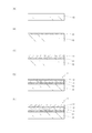
- FIG. 4 shows an outline of an example of a process for manufacturing a photomask blank, and shows cross-sectional views in each process.
- a transparent substrate 10 is prepared, and as shown in FIG. 4B, a first film 11 is formed on the transparent substrate 10 (of the first film). Forming step).
- the second film 12 is formed on the first film 11 (second film forming step), whereby the photo of the first mode shown in FIG. 1A or FIG. Mask blank 1 can be obtained.
- a photoresist film 13 is further formed on the second film 12 (photoresist film forming step), so that FIG. ) Or the photomask blank 1 of the second embodiment shown in FIG. 4D can be obtained.
- FIG. 5 shows an outline of an example of a process for manufacturing a photomask from the photomask blank of the first mode shown in FIG. 4C or the photomask blank of the second mode shown in FIG. 4D. Sectional drawing in each process is shown.
- a photoresist film 13 is formed on the second film 12 (photoresist film forming step).
- the photoresist film 13 is patterned by a known method, for example, a method such as electron beam drawing, and the resist after pattern drawing is formed. Patterning is performed by developing to form a resist pattern 13a (resist pattern forming step).
- FIG. 5 shows an outline of an example of a process for manufacturing a photomask from the photomask blank of the first mode shown in FIG. 4C or the photomask blank of the second mode shown in FIG. 4D. Sectional drawing in each process is shown.
- a photoresist film 13 is formed on the second film 12 (photoresist film forming step).
- the photoresist film 13 is patterned
- the second film 12 is patterned by fluorine-based dry etching using the resist pattern 13a as an etching mask to form a mask pattern 12a of the second film ( (Step of forming mask pattern of second film)
- the resist pattern 13a is peeled off.
- the resist pattern 13a is peeled off after the second film 12 is etched.
- the resist pattern 13a is left without being peeled in this step, and after etching the first film 11 described later. It may be peeled off.
- the first film 11 is patterned by chlorine oxygen dry etching to form a mask pattern 11a of the first film (of the first film).
- Step of forming mask pattern When the resist pattern 13a is left, the resist pattern 13a is peeled off at this stage, and the second film shown in FIG. 1B or FIG. A photomask 101 in the case of a film that functions as a part of the film can be obtained. Further, when the second film is a film that functions as a part of the optical film, a resist pattern is additionally formed as necessary, and then a part of the mask pattern 11a of the second film is peeled off. It is also possible.
- the second film is a processing auxiliary film
- a resist pattern is additionally formed as necessary, and then the entire mask pattern 12a of the second film is peeled off, whereby FIG. Alternatively, a photomask 102 as shown in FIG. 5E can be obtained.
- the photomask of the first and second aspects includes a transparent substrate and a photomask pattern of the first film or a photomask pattern of the first film and a photomask pattern of the second film.
- a transmission type photomask can be manufactured, and the mask pattern of the first film can be formed from the first film formed on the transparent substrate of the photomask blank.
- the photomask blanks of the first and second modes in which a phase shift film such as a halftone phase shift film is formed between the transparent substrate and the first film That is, a method of manufacturing a phase shift mask blank such as a halftone phase shift mask blank, a method of manufacturing a photomask from the photomask blank, and a method of forming a mask pattern of the first film at that time will be described.
- FIG. 6 shows an outline of another example of a process for manufacturing a photomask blank, and shows cross-sectional views in each process.
- a transparent substrate 10 is prepared, and as shown in FIG. 6B, a phase shift film 14 is formed on the transparent substrate 10 (phase shift film forming step). ).
- the first film 11 is formed on the phase shift film 14 (first film forming step).
- the second film 12 is formed over the first film 11 (second film forming step), whereby the photo of the first mode shown in FIG. 2A or FIG. Mask blank 1 can be obtained.
- a photoresist film 13 is further formed on the second film 12 (photoresist film forming step), whereby FIG. ) Or the photomask blank 1 shown in FIG. 6E can be obtained.
- FIG. 7 shows an outline of an example of a process for manufacturing a photomask from the photomask blank of the first mode shown in FIG. 6D or the photomask blank of the second mode shown in FIG. Sectional drawing in each process is shown.
- a photoresist film is formed on the second film 12 (photoresist film forming step).
- the photoresist film 13 is patterned by a known method such as electron beam drawing, and the resist after pattern drawing is formed. Patterning is performed by developing to form a resist pattern 13a (resist pattern forming step).
- FIG. 7 shows an outline of an example of a process for manufacturing a photomask from the photomask blank of the first mode shown in FIG. 6D or the photomask blank of the second mode shown in FIG. Sectional drawing in each process is shown.
- the second film 12 is patterned by fluorine-based dry etching using the resist pattern 13a as an etching mask to form a mask pattern 12a of the second film ( (Step of forming mask pattern of second film)
- the resist pattern 13a is peeled off.
- the resist pattern 13a is peeled off after the second film 12 is etched.
- the resist pattern 13a is left without being peeled in this step, and after etching the first film 11 described later. It may be peeled off.
- the first film 11 is patterned by chlorine-oxygen-based dry etching using the mask pattern 12a of the second film as an etching mask, thereby masking the first film.
- the pattern 11a is formed (step of forming the mask pattern of the first film) and the resist pattern 13a is left, the resist pattern 13a is peeled off at this stage.
- the phase shift film 14 is patterned by fluorine-based dry etching to form the mask pattern 14a of the phase shift film, and the mask pattern of the second film
- the photomask 103 in the case where the first film shown in FIG.
- FIG. 7E is used as a film that functions as part of the optical film can be obtained by peeling 12a.
- a resist pattern is additionally formed as necessary, and then a part of the mask pattern 11a of the first film is peeled off. It is also possible.
- a resist pattern is additionally formed as necessary, and then the entire mask pattern 11a of the first film is peeled off, whereby FIG. A photomask 104 as shown in FIG.
- the photomask of the first and second aspects is a transparent substrate and a phase shift film mask pattern such as a halftone phase shift film, or a phase shift film mask pattern such as a halftone phase shift film, and
- a transmissive photomask having a photomask pattern of a first film that is, a phase shift mask such as a halftone phase shift mask can be manufactured, and the first film formed on the transparent substrate of the photomask blank
- the mask pattern of the first film can be formed.
- the photomask blank of the present invention is a photomask blank for forming a photomask pattern having a width of 45 nm or less on a photomask using exposure light having a wavelength of 200 nm or less, and a width of 40 nm or less on a transfer object. It is suitable as a photomask blank for producing a transmissive photomask used for photolithography (optical lithography) for forming a fine pattern with a width of preferably 30 nm or less, more preferably 20 nm or less, and even more preferably 10 nm or less.
- Example 1 A phase shift film (thickness 75 nm) made of MoSiON was formed by sputtering on a 152 mm square quartz substrate having a thickness of about 6 mm.
- As the sputtering gas oxygen gas, nitrogen gas, and argon gas were used, and as the target, two types of MoSi 2 target and Si target were used, and the film was formed while rotating the substrate at 30 rpm.
- the composition of this phase shift film was measured by ESCA using an X-ray photoelectron spectrometer (K-Alpha manufactured by Thermo Fisher Scientific Co., Ltd.).
- Mo: Si: O: N 1: 4: 1: 4 (atomic ratio).
- a light shielding film consisting of two layers of a CrN layer (thickness 30 nm) and a CrON layer (thickness 20 nm) is sputtered as a first film from the quartz substrate side. Formed by the law.
- the CrN layer was formed using nitrogen gas and argon gas
- the CrON layer was formed using oxygen gas, nitrogen gas and argon gas
- the target was formed using metal chromium while rotating the substrate at 30 rpm.
- HMDS hexamethyldisilazane
- SEBN-1637 a negative type chemically amplified electron beam resist manufactured by Shin-Etsu Chemical Co., Ltd.
Landscapes
- Physics & Mathematics (AREA)
- General Physics & Mathematics (AREA)
- Preparing Plates And Mask In Photomechanical Process (AREA)
Abstract
Description
[1] 被転写物上に、波長200nm以下の露光光を用いてパターンを形成するフォトリソグラフィに用いる透過型フォトマスクを製造するためのフォトマスクブランクであって、
透明基板と、
該透明基板上に形成され、塩素ガスと酸素ガスとの混合ガスによる塩素酸素系ドライエッチングでエッチングされ、かつフッ素を含有するガスによるフッ素系ドライエッチングに耐性を有する材料で構成された第1の膜と、
該第1の膜に接して形成され、ケイ素と酸素、又はケイ素と酸素と窒素とからなり、かつ上記第1の膜をエッチングする上記塩素酸素系ドライエッチングでは実質的にエッチングされない材料で構成された第2の膜とを有し、該第2の膜がSi-Si結合を有する材料で構成されていることを特徴とするフォトマスクブランク。
[2] 更に、上記第2の膜に接して形成され、膜厚が150nm以下のフォトレジスト膜を有し、該フォトレジスト膜が化学増幅型レジスト膜であることを特徴とする[1]記載のフォトマスクブランク。
[3] 上記第2の膜が、酸素を1原子%以上66原子%以下の割合で含有することを特徴とする[1]又は[2]記載のフォトマスクブランク。
[4] 上記第2の膜の膜厚が2nm以上20nm以下であることを特徴とする[1]乃至[3]のいずれかに記載のフォトマスクブランク。
[5] 上記第2の膜のシート抵抗が1×10¹¹Ω/□以下であることを特徴とする[1]乃至[4]のいずれかに記載のフォトマスクブランク。
[6] 上記透明基板と第1の膜との間に、位相シフト膜が形成されていることを特徴とする[1]乃至[5]のいずれかに記載のフォトマスクブランク。
[7] 透明基板上に、塩素ガスと酸素ガスとの混合ガスによる塩素酸素系ドライエッチングでエッチングされ、かつフッ素を含有するガスによるフッ素系ドライエッチングに耐性を有する材料で構成された第1の膜を形成する工程、
該第1の膜に接して、ケイ素と酸素、又はケイ素と酸素と窒素とからなり、Si-Si結合を有し、かつ上記第1の膜をエッチングする上記塩素酸素系ドライエッチングでは実質的にエッチングされない材料で構成された第2の膜を形成する工程、
該第2の膜に接して、膜厚が150nm以下の化学増幅型レジスト膜を形成する工程、
該化学増幅型レジスト膜をパターニングしてレジストパターンを形成する工程、
該レジストパターンをエッチングマスクとして、上記第2の膜を上記フッ素系ドライエッチングによりパターニングして、第2の膜のマスクパターンを形成する工程、及び
上記第2の膜のマスクパターンをエッチングマスクとして、上記第1の膜を上記塩素酸素系ドライエッチングによりパターニングして、第1の膜のマスクパターンを形成する工程
を含むことを特徴とするフォトマスクの製造方法。
[8] 上記透明基板と上記第1の膜との間に、位相シフト膜を形成する工程、及び
上記第1の膜のマスクパターンをエッチングマスクとして、上記位相シフト膜をフッ素系ドライエッチングによりパターニングして、位相シフト膜のマスクパターンを形成する工程
を含むことを特徴とする[7]記載の製造方法。
[9] 被転写物上に、波長200nm以下の露光光を用いて、幅30nm以下の微細パターンを形成するフォトリソグラフィに用いる透過型フォトマスクを製造することを特徴とする[7]又は[8]記載の製造方法。
[10] フォトマスクブランクの透明基板上に形成された膜であり、塩素ガスと酸素ガスとの混合ガスによる塩素酸素系ドライエッチングでエッチングされ、かつフッ素を含有するガスによるフッ素系ドライエッチングに耐性を有する材料で構成された第1の膜から、該第1の膜のマスクパターンを形成する方法であって、
上記第1の膜に接して、ケイ素と酸素、又はケイ素と酸素と窒素とからなり、Si-Si結合を有し、かつ上記第1の膜をエッチングする上記塩素酸素系ドライエッチングでは実質的にエッチングされない材料で構成された第2の膜を形成する工程、
該第2の膜に接して、膜厚が150nm以下の化学増幅型レジスト膜を形成する工程、
該化学増幅型レジスト膜をパターニングしてレジストパターンを形成する工程、
該レジストパターンをエッチングマスクとして、上記第2の膜を上記フッ素系ドライエッチングによりパターニングして、第2の膜のマスクパターンを形成する工程、及び
該第2の膜のマスクパターンをエッチングマスクとして、上記第1の膜を上記塩素酸素系ドライエッチングによりパターニングして、第1の膜のマスクパターンを形成する工程
を含むことを特徴とするマスクパターン形成方法。
本発明の第1の態様のフォトマスクブランクは、透明基板と、透明基板上に形成された第1の膜と、第1の膜に接して形成された第2の膜とを有する。具体的には、図1(A)に示されるフォトマスクブランクが例示される。図1(A)は、本発明の第1の態様のフォトマスクブランクの一例を示す断面図であり、このフォトマスクブランク1は、透明基板10上に、透明基板10に接して形成された第1の膜11と、第1の膜11に接して形成された第2の膜12とを備える。
152mm角、厚さ約6mmの石英基板上に、MoSiONからなる位相シフト膜(厚さ75nm)をスパッタ法で形成した。スパッタガスとしては、酸素ガスと窒素ガスとアルゴンガスとを用い、ターゲットとしては、MoSi2ターゲットとSiターゲットとの2種類を用いて、基板を30rpmで回転させながら成膜した。この位相シフト膜の組成を、X線光電子分光装置(サーモフィッシャーサイエンティフィック(株)製 K-Alpha)を用いたESCAにより測定したところ、Mo:Si:O:N=1:4:1:4(原子比)であった。
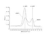
152mm角、厚さ約6mmの石英基板上に、実施例1と同様の位相シフト膜及び遮光膜を形成した。次に、遮光膜の上に、SiO2からなる単層(厚さ5nm)のエッチングマスク膜(ハードマスク膜)をスパッタ法で形成した。スパッタガスとしては、酸素ガスとアルゴンとを用い、ターゲットとしてはSiを用いて、基板を30rpmで回転させながら成膜した。このエッチングマスク膜の組成をESCAで測定したところ、Si:O=1:2(原子比)であった。また、ESCAによるXPSプロファイルを図8に示す。XPSプロファイルから、Si-Si結合の結合エネルギーは確認されず、Si-Si結合が存在しないことが確認された。更に、実施例1と同様にしてフォトレジスト膜を形成して、フォトマスクブランクを得た。
10 透明基板
11 第1の膜
11a 第1の膜のマスクパターン
12 第2の膜
12a 第2の膜のマスクパターン
13 フォトレジスト膜
13a レジストパターン
14 位相シフト膜
14a 位相シフト膜のパターン
15 遮光膜
101,102,103,104 フォトマスク
Claims (10)
- 被転写物上に、波長200nm以下の露光光を用いてパターンを形成するフォトリソグラフィに用いる透過型フォトマスクを製造するためのフォトマスクブランクであって、
透明基板と、
該透明基板上に形成され、塩素ガスと酸素ガスとの混合ガスによる塩素酸素系ドライエッチングでエッチングされ、かつフッ素を含有するガスによるフッ素系ドライエッチングに耐性を有する材料で構成された第1の膜と、
該第1の膜に接して形成され、ケイ素と酸素、又はケイ素と酸素と窒素とからなり、かつ上記第1の膜をエッチングする上記塩素酸素系ドライエッチングでは実質的にエッチングされない材料で構成された第2の膜とを有し、該第2の膜がSi-Si結合を有する材料で構成されていることを特徴とするフォトマスクブランク。 - 更に、上記第2の膜に接して形成され、膜厚が150nm以下のフォトレジスト膜を有し、該フォトレジスト膜が化学増幅型レジスト膜であることを特徴とする請求項1記載のフォトマスクブランク。
- 上記第2の膜が、酸素を1原子%以上66原子%以下の割合で含有することを特徴とする請求項1又は2記載のフォトマスクブランク。
- 上記第2の膜の膜厚が2nm以上20nm以下であることを特徴とする請求項1乃至3のいずれか1項記載のフォトマスクブランク。
- 上記第2の膜のシート抵抗が1×10¹¹Ω/□以下であることを特徴とする請求項1乃至4のいずれか1項記載のフォトマスクブランク。
- 上記透明基板と第1の膜との間に、位相シフト膜が形成されていることを特徴とする請求項1乃至5のいずれか1項記載のフォトマスクブランク。
- 透明基板上に、塩素ガスと酸素ガスとの混合ガスによる塩素酸素系ドライエッチングでエッチングされ、かつフッ素を含有するガスによるフッ素系ドライエッチングに耐性を有する材料で構成された第1の膜を形成する工程、
該第1の膜に接して、ケイ素と酸素、又はケイ素と酸素と窒素とからなり、Si-Si結合を有し、かつ上記第1の膜をエッチングする上記塩素酸素系ドライエッチングでは実質的にエッチングされない材料で構成された第2の膜を形成する工程、
該第2の膜に接して、膜厚が150nm以下の化学増幅型レジスト膜を形成する工程、
該化学増幅型レジスト膜をパターニングしてレジストパターンを形成する工程、
該レジストパターンをエッチングマスクとして、上記第2の膜を上記フッ素系ドライエッチングによりパターニングして、第2の膜のマスクパターンを形成する工程、及び
上記第2の膜のマスクパターンをエッチングマスクとして、上記第1の膜を上記塩素酸素系ドライエッチングによりパターニングして、第1の膜のマスクパターンを形成する工程
を含むことを特徴とするフォトマスクの製造方法。 - 上記透明基板と上記第1の膜との間に、位相シフト膜を形成する工程、及び
上記第1の膜のマスクパターンをエッチングマスクとして、上記位相シフト膜をフッ素系ドライエッチングによりパターニングして、位相シフト膜のマスクパターンを形成する工程
を含むことを特徴とする請求項7記載の製造方法。 - 被転写物上に、波長200nm以下の露光光を用いて、幅30nm以下の微細パターンを形成するフォトリソグラフィに用いる透過型フォトマスクを製造することを特徴とする請求項7又は8記載の製造方法。
- フォトマスクブランクの透明基板上に形成された膜であり、塩素ガスと酸素ガスとの混合ガスによる塩素酸素系ドライエッチングでエッチングされ、かつフッ素を含有するガスによるフッ素系ドライエッチングに耐性を有する材料で構成された第1の膜から、該第1の膜のマスクパターンを形成する方法であって、
上記第1の膜に接して、ケイ素と酸素、又はケイ素と酸素と窒素とからなり、Si-Si結合を有し、かつ上記第1の膜をエッチングする上記塩素酸素系ドライエッチングでは実質的にエッチングされない材料で構成された第2の膜を形成する工程、
該第2の膜に接して、膜厚が150nm以下の化学増幅型レジスト膜を形成する工程、
該化学増幅型レジスト膜をパターニングしてレジストパターンを形成する工程、
該レジストパターンをエッチングマスクとして、上記第2の膜を上記フッ素系ドライエッチングによりパターニングして、第2の膜のマスクパターンを形成する工程、及び
該第2の膜のマスクパターンをエッチングマスクとして、上記第1の膜を上記塩素酸素系ドライエッチングによりパターニングして、第1の膜のマスクパターンを形成する工程
を含むことを特徴とするマスクパターン形成方法。
Priority Applications (5)
| Application Number | Priority Date | Filing Date | Title |
|---|---|---|---|
| EP16758738.5A EP3267253B1 (en) | 2015-03-04 | 2016-02-15 | Photomask blank, method for manufacturing photomask, and mask pattern formation method |
| SG11201705165QA SG11201705165QA (en) | 2015-03-04 | 2016-02-15 | Photomask blank, method for manufacturing photomask, and mask pattern formation method |
| KR1020177025593A KR102140572B1 (ko) | 2015-03-04 | 2016-02-15 | 포토 마스크 블랭크, 포토 마스크의 제조 방법 및 마스크 패턴 형성 방법 |
| US15/542,296 US10585345B2 (en) | 2015-03-04 | 2016-02-15 | Photomask blank, method for manufacturing photomask, and mask pattern formation method |
| CN201680013518.6A CN107430328B (zh) | 2015-03-04 | 2016-02-15 | 光掩模坯、光掩模的制造方法和掩模图案形成方法 |
Applications Claiming Priority (4)
| Application Number | Priority Date | Filing Date | Title |
|---|---|---|---|
| JP2015042216 | 2015-03-04 | ||
| JP2015-042216 | 2015-03-04 | ||
| JP2016021469A JP6601245B2 (ja) | 2015-03-04 | 2016-02-08 | フォトマスクブランク、フォトマスクの製造方法及びマスクパターン形成方法 |
| JP2016-021469 | 2016-02-08 |
Publications (1)
| Publication Number | Publication Date |
|---|---|
| WO2016140044A1 true WO2016140044A1 (ja) | 2016-09-09 |
Family
ID=56848060
Family Applications (1)
| Application Number | Title | Priority Date | Filing Date |
|---|---|---|---|
| PCT/JP2016/054225 Ceased WO2016140044A1 (ja) | 2015-03-04 | 2016-02-15 | フォトマスクブランク、フォトマスクの製造方法及びマスクパターン形成方法 |
Country Status (1)
| Country | Link |
|---|---|
| WO (1) | WO2016140044A1 (ja) |
Cited By (3)
| Publication number | Priority date | Publication date | Assignee | Title |
|---|---|---|---|---|
| EP3415987A1 (en) * | 2017-06-13 | 2018-12-19 | Shin-Etsu Chemical Co., Ltd. | Photomask blank and making method |
| JP2020126223A (ja) * | 2019-02-05 | 2020-08-20 | 凸版印刷株式会社 | クロムブランクス、フォトマスクの製造方法、およびインプリントモールドの製造方法 |
| JP2020154054A (ja) * | 2019-03-18 | 2020-09-24 | Hoya株式会社 | マスクブランク、転写用マスクの製造方法、及び半導体デバイスの製造方法 |
Citations (6)
| Publication number | Priority date | Publication date | Assignee | Title |
|---|---|---|---|---|
| JP2008026500A (ja) * | 2006-07-20 | 2008-02-07 | Dainippon Printing Co Ltd | 高ドライエッチング耐性ポリマー層を付加したフォトマスクブランクスおよびそれを用いたフォトマスクの製造方法 |
| JP2012068314A (ja) * | 2010-09-21 | 2012-04-05 | Shin Etsu Chem Co Ltd | フォトマスクブランク及びその加工方法 |
| WO2012043695A1 (ja) * | 2010-09-30 | 2012-04-05 | Hoya株式会社 | マスクブランク及びその製造方法並びに転写用マスク |
| JP2013238776A (ja) * | 2012-05-16 | 2013-11-28 | Shin Etsu Chem Co Ltd | ハーフトーン位相シフトマスクブランク及びハーフトーン位相シフトマスクの製造方法 |
| JP2014137388A (ja) * | 2013-01-15 | 2014-07-28 | Hoya Corp | マスクブランク、位相シフトマスクおよびこれらの製造方法 |
| JP2016035546A (ja) * | 2013-09-25 | 2016-03-17 | 信越化学工業株式会社 | フォトマスクブランクおよびその製造方法 |
-
2016
- 2016-02-15 WO PCT/JP2016/054225 patent/WO2016140044A1/ja not_active Ceased
Patent Citations (6)
| Publication number | Priority date | Publication date | Assignee | Title |
|---|---|---|---|---|
| JP2008026500A (ja) * | 2006-07-20 | 2008-02-07 | Dainippon Printing Co Ltd | 高ドライエッチング耐性ポリマー層を付加したフォトマスクブランクスおよびそれを用いたフォトマスクの製造方法 |
| JP2012068314A (ja) * | 2010-09-21 | 2012-04-05 | Shin Etsu Chem Co Ltd | フォトマスクブランク及びその加工方法 |
| WO2012043695A1 (ja) * | 2010-09-30 | 2012-04-05 | Hoya株式会社 | マスクブランク及びその製造方法並びに転写用マスク |
| JP2013238776A (ja) * | 2012-05-16 | 2013-11-28 | Shin Etsu Chem Co Ltd | ハーフトーン位相シフトマスクブランク及びハーフトーン位相シフトマスクの製造方法 |
| JP2014137388A (ja) * | 2013-01-15 | 2014-07-28 | Hoya Corp | マスクブランク、位相シフトマスクおよびこれらの製造方法 |
| JP2016035546A (ja) * | 2013-09-25 | 2016-03-17 | 信越化学工業株式会社 | フォトマスクブランクおよびその製造方法 |
Cited By (12)
| Publication number | Priority date | Publication date | Assignee | Title |
|---|---|---|---|---|
| EP3415987A1 (en) * | 2017-06-13 | 2018-12-19 | Shin-Etsu Chemical Co., Ltd. | Photomask blank and making method |
| CN109085737A (zh) * | 2017-06-13 | 2018-12-25 | 信越化学工业株式会社 | 光掩模坯料及制造方法 |
| JP2019002973A (ja) * | 2017-06-13 | 2019-01-10 | 信越化学工業株式会社 | フォトマスクブランク及びその製造方法 |
| US11061319B2 (en) | 2017-06-13 | 2021-07-13 | Shin-Etsu Chemical Co., Ltd. | Photomask blank and making method |
| CN109085737B (zh) * | 2017-06-13 | 2024-07-09 | 信越化学工业株式会社 | 光掩模坯料及制造方法 |
| JP2020126223A (ja) * | 2019-02-05 | 2020-08-20 | 凸版印刷株式会社 | クロムブランクス、フォトマスクの製造方法、およびインプリントモールドの製造方法 |
| JP7491681B2 (ja) | 2019-02-05 | 2024-05-28 | 株式会社トッパンフォトマスク | クロムブランクス、フォトマスクの製造方法、およびインプリントモールドの製造方法 |
| JP2020154054A (ja) * | 2019-03-18 | 2020-09-24 | Hoya株式会社 | マスクブランク、転写用マスクの製造方法、及び半導体デバイスの製造方法 |
| WO2020189168A1 (ja) * | 2019-03-18 | 2020-09-24 | Hoya株式会社 | マスクブランク、転写用マスクの製造方法、及び半導体デバイスの製造方法 |
| US20220214608A1 (en) * | 2019-03-18 | 2022-07-07 | Hoya Corporation | Mask blank, method for manufacturing transfer mask, and method for manufacturing semiconductor device |
| JP7313166B2 (ja) | 2019-03-18 | 2023-07-24 | Hoya株式会社 | マスクブランク、転写用マスクの製造方法、及び半導体デバイスの製造方法 |
| US12153338B2 (en) * | 2019-03-18 | 2024-11-26 | Hoya Corporation | Mask blank, method for manufacturing transfer mask, and method for manufacturing semiconductor device |
Similar Documents
| Publication | Publication Date | Title |
|---|---|---|
| JP6601245B2 (ja) | フォトマスクブランク、フォトマスクの製造方法及びマスクパターン形成方法 | |
| JP5345333B2 (ja) | フォトマスクブランク、フォトマスク及びその製造方法 | |
| US8043771B2 (en) | Phase shift mask blank and method of manufacturing phase shift mask | |
| EP2863258B1 (en) | Photomask blank and method for manufacturing photomask blank | |
| JP5704754B2 (ja) | マスクブランク及び転写用マスクの製造方法 | |
| KR101680865B1 (ko) | 포토마스크의 제조방법 | |
| KR102195696B1 (ko) | 하프톤 위상 시프트형 포토마스크 블랭크 | |
| JP2010079110A (ja) | マスクブランク及び転写用マスクの製造方法 | |
| JP6398927B2 (ja) | フォトマスクブランク、その製造方法及びフォトマスク | |
| TWI613505B (zh) | 空白光罩之製造方法 | |
| WO2019188397A1 (ja) | マスクブランク、位相シフトマスク及び半導体デバイスの製造方法 | |
| JP5294227B2 (ja) | マスクブランク及び転写マスクの製造方法 | |
| WO2016140044A1 (ja) | フォトマスクブランク、フォトマスクの製造方法及びマスクパターン形成方法 | |
| JP2009092823A (ja) | フォトマスクブランクスおよびフォトマスク | |
| JP5701946B2 (ja) | 位相シフトマスクの製造方法 | |
| KR102757115B1 (ko) | 포토마스크의 제조 방법 및 포토마스크 블랭크 | |
| JP2004258456A (ja) | ハーフトーン型位相シフトマスク用ブランク及びそれを用いたハーフトーン型位相シフトマスク |
Legal Events
| Date | Code | Title | Description |
|---|---|---|---|
| 121 | Ep: the epo has been informed by wipo that ep was designated in this application |
Ref document number: 16758738 Country of ref document: EP Kind code of ref document: A1 |
|
| REEP | Request for entry into the european phase |
Ref document number: 2016758738 Country of ref document: EP |
|
| WWE | Wipo information: entry into national phase |
Ref document number: 15542296 Country of ref document: US |
|
| WWE | Wipo information: entry into national phase |
Ref document number: 11201705165Q Country of ref document: SG |
|
| NENP | Non-entry into the national phase |
Ref country code: DE |
|
| ENP | Entry into the national phase |
Ref document number: 20177025593 Country of ref document: KR Kind code of ref document: A |