WO2016143366A1 - 透明導電膜付ガラス基板及びその製造方法 - Google Patents
透明導電膜付ガラス基板及びその製造方法 Download PDFInfo
- Publication number
- WO2016143366A1 WO2016143366A1 PCT/JP2016/050470 JP2016050470W WO2016143366A1 WO 2016143366 A1 WO2016143366 A1 WO 2016143366A1 JP 2016050470 W JP2016050470 W JP 2016050470W WO 2016143366 A1 WO2016143366 A1 WO 2016143366A1
- Authority
- WO
- WIPO (PCT)
- Prior art keywords
- conductive film
- transparent conductive
- glass substrate
- linear portion
- laser
- Prior art date
- Legal status (The legal status is an assumption and is not a legal conclusion. Google has not performed a legal analysis and makes no representation as to the accuracy of the status listed.)
- Ceased
Links
Images


Classifications
-
- C—CHEMISTRY; METALLURGY
- C03—GLASS; MINERAL OR SLAG WOOL
- C03C—CHEMICAL COMPOSITION OF GLASSES, GLAZES OR VITREOUS ENAMELS; SURFACE TREATMENT OF GLASS; SURFACE TREATMENT OF FIBRES OR FILAMENTS MADE FROM GLASS, MINERALS OR SLAGS; JOINING GLASS TO GLASS OR OTHER MATERIALS
- C03C3/00—Glass compositions
- C03C3/04—Glass compositions containing silica
- C03C3/062—Glass compositions containing silica with less than 40% silica by weight
- C03C3/064—Glass compositions containing silica with less than 40% silica by weight containing boron
-
- C—CHEMISTRY; METALLURGY
- C03—GLASS; MINERAL OR SLAG WOOL
- C03C—CHEMICAL COMPOSITION OF GLASSES, GLAZES OR VITREOUS ENAMELS; SURFACE TREATMENT OF GLASS; SURFACE TREATMENT OF FIBRES OR FILAMENTS MADE FROM GLASS, MINERALS OR SLAGS; JOINING GLASS TO GLASS OR OTHER MATERIALS
- C03C17/00—Surface treatment of glass, not in the form of fibres or filaments, by coating
- C03C17/34—Surface treatment of glass, not in the form of fibres or filaments, by coating with at least two coatings having different compositions
-
- B—PERFORMING OPERATIONS; TRANSPORTING
- B23—MACHINE TOOLS; METAL-WORKING NOT OTHERWISE PROVIDED FOR
- B23K—SOLDERING OR UNSOLDERING; WELDING; CLADDING OR PLATING BY SOLDERING OR WELDING; CUTTING BY APPLYING HEAT LOCALLY, e.g. FLAME CUTTING; WORKING BY LASER BEAM
- B23K26/00—Working by laser beam, e.g. welding, cutting or boring
- B23K26/351—Working by laser beam, e.g. welding, cutting or boring for trimming or tuning of electrical components
-
- C—CHEMISTRY; METALLURGY
- C03—GLASS; MINERAL OR SLAG WOOL
- C03C—CHEMICAL COMPOSITION OF GLASSES, GLAZES OR VITREOUS ENAMELS; SURFACE TREATMENT OF GLASS; SURFACE TREATMENT OF FIBRES OR FILAMENTS MADE FROM GLASS, MINERALS OR SLAGS; JOINING GLASS TO GLASS OR OTHER MATERIALS
- C03C17/00—Surface treatment of glass, not in the form of fibres or filaments, by coating
- C03C17/001—General methods for coating; Devices therefor
- C03C17/002—General methods for coating; Devices therefor for flat glass, e.g. float glass
-
- C—CHEMISTRY; METALLURGY
- C03—GLASS; MINERAL OR SLAG WOOL
- C03C—CHEMICAL COMPOSITION OF GLASSES, GLAZES OR VITREOUS ENAMELS; SURFACE TREATMENT OF GLASS; SURFACE TREATMENT OF FIBRES OR FILAMENTS MADE FROM GLASS, MINERALS OR SLAGS; JOINING GLASS TO GLASS OR OTHER MATERIALS
- C03C17/00—Surface treatment of glass, not in the form of fibres or filaments, by coating
- C03C17/34—Surface treatment of glass, not in the form of fibres or filaments, by coating with at least two coatings having different compositions
- C03C17/3411—Surface treatment of glass, not in the form of fibres or filaments, by coating with at least two coatings having different compositions with at least two coatings of inorganic materials
- C03C17/3417—Surface treatment of glass, not in the form of fibres or filaments, by coating with at least two coatings having different compositions with at least two coatings of inorganic materials all coatings being oxide coatings
-
- C—CHEMISTRY; METALLURGY
- C03—GLASS; MINERAL OR SLAG WOOL
- C03C—CHEMICAL COMPOSITION OF GLASSES, GLAZES OR VITREOUS ENAMELS; SURFACE TREATMENT OF GLASS; SURFACE TREATMENT OF FIBRES OR FILAMENTS MADE FROM GLASS, MINERALS OR SLAGS; JOINING GLASS TO GLASS OR OTHER MATERIALS
- C03C19/00—Surface treatment of glass, not in the form of fibres or filaments, by mechanical means
-
- H—ELECTRICITY
- H05—ELECTRIC TECHNIQUES NOT OTHERWISE PROVIDED FOR
- H05B—ELECTRIC HEATING; ELECTRIC LIGHT SOURCES NOT OTHERWISE PROVIDED FOR; CIRCUIT ARRANGEMENTS FOR ELECTRIC LIGHT SOURCES, IN GENERAL
- H05B33/00—Electroluminescent light sources
- H05B33/02—Details
-
- H—ELECTRICITY
- H05—ELECTRIC TECHNIQUES NOT OTHERWISE PROVIDED FOR
- H05B—ELECTRIC HEATING; ELECTRIC LIGHT SOURCES NOT OTHERWISE PROVIDED FOR; CIRCUIT ARRANGEMENTS FOR ELECTRIC LIGHT SOURCES, IN GENERAL
- H05B33/00—Electroluminescent light sources
- H05B33/12—Light sources with substantially two-dimensional [2D] radiating surfaces
- H05B33/26—Light sources with substantially two-dimensional [2D] radiating surfaces characterised by the composition or arrangement of the conductive material used as an electrode
-
- H—ELECTRICITY
- H10—SEMICONDUCTOR DEVICES; ELECTRIC SOLID-STATE DEVICES NOT OTHERWISE PROVIDED FOR
- H10K—ORGANIC ELECTRIC SOLID-STATE DEVICES
- H10K50/00—Organic light-emitting devices
- H10K50/80—Constructional details
-
- H—ELECTRICITY
- H10—SEMICONDUCTOR DEVICES; ELECTRIC SOLID-STATE DEVICES NOT OTHERWISE PROVIDED FOR
- H10K—ORGANIC ELECTRIC SOLID-STATE DEVICES
- H10K50/00—Organic light-emitting devices
- H10K50/80—Constructional details
- H10K50/805—Electrodes
-
- H—ELECTRICITY
- H10—SEMICONDUCTOR DEVICES; ELECTRIC SOLID-STATE DEVICES NOT OTHERWISE PROVIDED FOR
- H10K—ORGANIC ELECTRIC SOLID-STATE DEVICES
- H10K50/00—Organic light-emitting devices
- H10K50/80—Constructional details
- H10K50/85—Arrangements for extracting light from the devices
-
- H—ELECTRICITY
- H10—SEMICONDUCTOR DEVICES; ELECTRIC SOLID-STATE DEVICES NOT OTHERWISE PROVIDED FOR
- H10K—ORGANIC ELECTRIC SOLID-STATE DEVICES
- H10K50/00—Organic light-emitting devices
- H10K50/80—Constructional details
- H10K50/85—Arrangements for extracting light from the devices
- H10K50/858—Arrangements for extracting light from the devices comprising refractive means, e.g. lenses
-
- H—ELECTRICITY
- H10—SEMICONDUCTOR DEVICES; ELECTRIC SOLID-STATE DEVICES NOT OTHERWISE PROVIDED FOR
- H10K—ORGANIC ELECTRIC SOLID-STATE DEVICES
- H10K77/00—Constructional details of devices covered by this subclass and not covered by groups H10K10/80, H10K30/80, H10K50/80 or H10K59/80
- H10K77/10—Substrates, e.g. flexible substrates
-
- B—PERFORMING OPERATIONS; TRANSPORTING
- B32—LAYERED PRODUCTS
- B32B—LAYERED PRODUCTS, i.e. PRODUCTS BUILT-UP OF STRATA OF FLAT OR NON-FLAT, e.g. CELLULAR OR HONEYCOMB, FORM
- B32B2307/00—Properties of the layers or laminate
- B32B2307/20—Properties of the layers or laminate having particular electrical or magnetic properties, e.g. piezoelectric
- B32B2307/202—Conductive
-
- B—PERFORMING OPERATIONS; TRANSPORTING
- B32—LAYERED PRODUCTS
- B32B—LAYERED PRODUCTS, i.e. PRODUCTS BUILT-UP OF STRATA OF FLAT OR NON-FLAT, e.g. CELLULAR OR HONEYCOMB, FORM
- B32B2307/00—Properties of the layers or laminate
- B32B2307/40—Properties of the layers or laminate having particular optical properties
- B32B2307/412—Transparent
-
- C—CHEMISTRY; METALLURGY
- C03—GLASS; MINERAL OR SLAG WOOL
- C03C—CHEMICAL COMPOSITION OF GLASSES, GLAZES OR VITREOUS ENAMELS; SURFACE TREATMENT OF GLASS; SURFACE TREATMENT OF FIBRES OR FILAMENTS MADE FROM GLASS, MINERALS OR SLAGS; JOINING GLASS TO GLASS OR OTHER MATERIALS
- C03C2217/00—Coatings on glass
- C03C2217/70—Properties of coatings
- C03C2217/77—Coatings having a rough surface
-
- C—CHEMISTRY; METALLURGY
- C03—GLASS; MINERAL OR SLAG WOOL
- C03C—CHEMICAL COMPOSITION OF GLASSES, GLAZES OR VITREOUS ENAMELS; SURFACE TREATMENT OF GLASS; SURFACE TREATMENT OF FIBRES OR FILAMENTS MADE FROM GLASS, MINERALS OR SLAGS; JOINING GLASS TO GLASS OR OTHER MATERIALS
- C03C2217/00—Coatings on glass
- C03C2217/90—Other aspects of coatings
- C03C2217/94—Transparent conductive oxide layers [TCO] being part of a multilayer coating
-
- C—CHEMISTRY; METALLURGY
- C03—GLASS; MINERAL OR SLAG WOOL
- C03C—CHEMICAL COMPOSITION OF GLASSES, GLAZES OR VITREOUS ENAMELS; SURFACE TREATMENT OF GLASS; SURFACE TREATMENT OF FIBRES OR FILAMENTS MADE FROM GLASS, MINERALS OR SLAGS; JOINING GLASS TO GLASS OR OTHER MATERIALS
- C03C2218/00—Methods for coating glass
- C03C2218/30—Aspects of methods for coating glass not covered above
- C03C2218/32—After-treatment
- C03C2218/328—Partly or completely removing a coating
-
- H—ELECTRICITY
- H10—SEMICONDUCTOR DEVICES; ELECTRIC SOLID-STATE DEVICES NOT OTHERWISE PROVIDED FOR
- H10K—ORGANIC ELECTRIC SOLID-STATE DEVICES
- H10K50/00—Organic light-emitting devices
- H10K50/80—Constructional details
- H10K50/805—Electrodes
- H10K50/81—Anodes
-
- H—ELECTRICITY
- H10—SEMICONDUCTOR DEVICES; ELECTRIC SOLID-STATE DEVICES NOT OTHERWISE PROVIDED FOR
- H10K—ORGANIC ELECTRIC SOLID-STATE DEVICES
- H10K71/00—Manufacture or treatment specially adapted for the organic devices covered by this subclass
- H10K71/621—Providing a shape to conductive layers, e.g. patterning or selective deposition
-
- Y—GENERAL TAGGING OF NEW TECHNOLOGICAL DEVELOPMENTS; GENERAL TAGGING OF CROSS-SECTIONAL TECHNOLOGIES SPANNING OVER SEVERAL SECTIONS OF THE IPC; TECHNICAL SUBJECTS COVERED BY FORMER USPC CROSS-REFERENCE ART COLLECTIONS [XRACs] AND DIGESTS
- Y02—TECHNOLOGIES OR APPLICATIONS FOR MITIGATION OR ADAPTATION AGAINST CLIMATE CHANGE
- Y02E—REDUCTION OF GREENHOUSE GAS [GHG] EMISSIONS, RELATED TO ENERGY GENERATION, TRANSMISSION OR DISTRIBUTION
- Y02E10/00—Energy generation through renewable energy sources
- Y02E10/50—Photovoltaic [PV] energy
- Y02E10/549—Organic PV cells
-
- Y—GENERAL TAGGING OF NEW TECHNOLOGICAL DEVELOPMENTS; GENERAL TAGGING OF CROSS-SECTIONAL TECHNOLOGIES SPANNING OVER SEVERAL SECTIONS OF THE IPC; TECHNICAL SUBJECTS COVERED BY FORMER USPC CROSS-REFERENCE ART COLLECTIONS [XRACs] AND DIGESTS
- Y02—TECHNOLOGIES OR APPLICATIONS FOR MITIGATION OR ADAPTATION AGAINST CLIMATE CHANGE
- Y02P—CLIMATE CHANGE MITIGATION TECHNOLOGIES IN THE PRODUCTION OR PROCESSING OF GOODS
- Y02P70/00—Climate change mitigation technologies in the production process for final industrial or consumer products
- Y02P70/50—Manufacturing or production processes characterised by the final manufactured product
Definitions
- the present invention relates to a glass substrate with a transparent conductive film and a method for producing the same.
- a transparent conductive film used as an electrode is formed on a transparent substrate such as a glass substrate in a plasma display or an electroluminescent element, and the transparent conductive film is patterned with a laser (Patent Document 1 and Patent Document). 2).
- a base glass layer having a refractive index higher than that of the glass substrate may be provided between the glass substrate and the transparent conductive film in order to increase light extraction efficiency.
- the present inventors have found that when a base glass layer is provided, when the transparent conductive film is patterned with a laser, the transparent conductive film or the base glass layer is likely to be discolored or damaged.
- An object of the present invention is to provide a glass with a transparent conductive film that can suppress discoloration or damage to the transparent conductive film or the base glass layer when the transparent conductive film formed on the base glass layer is patterned with a laser. It is providing a board
- the glass substrate with a transparent conductive film of the present invention has a glass substrate, a base glass layer provided on the glass substrate, and a transparent conductive film provided on the base glass layer and patterned with a laser.
- the glass substrate is an underlying glass layer having an absorptance smaller than that of the transparent conductive film and greater than that of the glass substrate at the wavelength of the laser, and is patterned by the laser to form the transparent conductive film.
- the patterning region from which a part has been removed has a first linear portion, a second linear portion, and a connection portion that connects the first linear portion and the second linear portion, The angle formed by the first linear portion and the second linear portion is 120 ° or less, and the radius of curvature of the connection portion is 0.5 mm or more.
- Examples of the base glass layer include those containing bismuth-based glass.
- Examples of the base glass layer include those having a refractive index higher than that of the glass substrate.
- the laser for example, a femtosecond laser can be used.
- irregularities are formed on the surface of the glass substrate on which the base glass layer is provided.
- the glass substrate with a transparent conductive film of the present invention is used, for example, as a glass substrate for an organic electroluminescence element.
- the production method of the present invention is a method capable of producing the glass substrate with a transparent conductive film of the present invention, wherein a transparent conductive film before patterning is formed on a base glass layer.
- the transparent conductive film formed on the base glass layer is patterned with a laser, it is possible to suppress discoloration or damage to the transparent conductive film or the base glass layer.
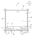
- FIG. 1 is a schematic cross-sectional view showing a glass substrate with a transparent conductive film according to an embodiment of the present invention.
- FIG. 2 is a schematic plan view showing a glass substrate with a transparent conductive film according to an embodiment of the present invention.
- FIG. 3 is a schematic plan view showing the first linear portion, the second linear portion, and the connecting portion shown in FIG. 2 in an enlarged manner.
- FIG. 4 is a schematic plan view showing an enlarged view of the first linear portion, the second linear portion, and the connection portion in the comparative example.
- FIG. 1 is a schematic cross-sectional view showing a glass substrate with a transparent conductive film according to an embodiment of the present invention.
- FIG. 2 is a schematic plan view showing a glass substrate with a transparent conductive film according to an embodiment of the present invention.
- FIG. 1 is a schematic cross-sectional view taken along the line II shown in FIG.
- the glass substrate 6 with a transparent conductive film of the present embodiment includes a glass substrate 1, a base glass layer 2 provided on the main surface 1 a of the glass substrate 1, and a main surface 2 a of the base glass layer 2. And a transparent conductive film 3 provided thereon. Concavities and convexities are formed on the main surface 1 a of the glass substrate 1. Therefore, the base glass layer 2 is provided on the main surface 1a on which irregularities are formed.
- the transparent conductive film 3 is formed with a patterning region 10 which is patterned by a laser and a part of the transparent conductive film 3 is removed.
- the transparent conductive film 3 is divided into a first electrode 4 and a second electrode 5 by a patterning region 10.
- the glass substrate 6 with a transparent conductive film of the present embodiment can be used as, for example, a glass substrate for an organic electroluminescence element.
- an organic electroluminescent layer is provided on the glass substrate 6 with a transparent conductive film.
- the light emitted from the organic electroluminescent layer and emitted from the organic electroluminescent layer passes through the transparent conductive film 3 and the glass substrate 1 and is extracted outside.
- the base glass layer 2 is provided between the transparent conductive film 3 and the glass substrate 1 in order to increase the extraction efficiency of light emitted from the organic electroluminescence layer.
- the refractive index nd of the organic electroluminescence layer is about 1.8 to 1.9
- the refractive index nd of the transparent conductive film 3 is about 1.9 to 2.0
- the rate nd is usually about 1.5.
- the base glass layer 2 is provided between the glass substrate 1 and the transparent conductive film 3, and the refractive index nd of the base glass layer 2 is made close to the refractive index nd of the transparent conductive film 3, thereby Light reflection can be suppressed, and light can be efficiently extracted outside. Therefore, the base glass layer 2 is generally formed of glass having a higher refractive index nd than the glass substrate 1, for example, 1.8 to 2.2. Examples of such glass include bismuth glass. Examples of the bismuth glass include glass containing 10 mol% or more of Bi 2 O 3 as a glass composition.
- the specific composition of the bismuth-based glass is Bi 2 O 3 10 to 35%, B 2 O 3 20 to 35%, SiO 2 over 5 to 35%, Al 2 O 3 0 to 10% in terms of mol%. , ZnO 0 to 10%, ZrO 2 1 to 8% glass, and in terms of mol%, Bi 2 O 3 10 to 35%, B 2 O 3 20 to 35%, SiO 2 + Al 2 O 3 21 to Examples thereof include glass containing 45%, ZnO 0 to 10%, and ZrO 2 0.1 to 10%.
- SiO 2 + Al 2 O 3 means the total content of SiO 2 and Al 2 O 3 .
- the glass substrate 1 with the irregularities formed on the main surface 1a can be produced, for example, by subjecting a glass plate having a flat surface to a method such as sandblasting, sol-gel spraying, or etching. Or it can also produce by press-molding a glass plate with the metal mold
- the surface roughness Ra of the main surface 1a is preferably in the range of 0.05 to 2 ⁇ m, for example, and more preferably in the range of 0.05 to 1.5 ⁇ m. If the surface roughness Ra of the main surface 1a is too small, sufficient light extraction efficiency may not be obtained. Moreover, when the surface roughness Ra of the main surface 1a is too large, sufficient light extraction efficiency cannot be obtained, and the thickness of the underlying glass layer 2 may have to be increased more than necessary.
- the transparent conductive film 3 for example, indium tin oxide (ITO), aluminum zinc oxide (AZO), indium zinc oxide (IZO), a composite having conductivity such as fluorine-doped tin oxide (FTO) is used.
- ITO indium tin oxide
- AZO aluminum zinc oxide
- IZO indium zinc oxide
- FTO fluorine-doped tin oxide
- An oxide thin film can be used.
- indium tin oxide is preferably used.
- the glass substrate 1 is not particularly limited as long as the light extraction efficiency is not reduced.
- the transparent conductive film 3 by patterning the transparent conductive film 3 with a laser, a part of the transparent conductive film 3 is removed and the patterning region 10 is formed.
- a laser a laser having a large absorption rate of the transparent conductive film 3 at the wavelength is used.
- the absorptance increases at a wavelength of 1000 nm or more.
- the ITO film can be removed by laser irradiation to form the patterning region 10.
- the present inventors pattern the transparent conductive film 3 with a laser, and when the transparent conductive film 3 is partially removed by laser irradiation, the transparent conductive film 3 or the underlying glass layer 2 is discolored or damaged. It has been found that may occur. In particular, it has been found that such discoloration and damage are likely to occur at the corner where the laser scanning direction changes in the vertical direction. When this cause was examined, when the laser scanning direction changes to the vertical direction, the scanning speed decreases and the laser irradiation time becomes relatively long, so heat is accumulated in that part, causing discoloration and damage. I found out. Further, it has been found that such a phenomenon occurs because the underlying glass layer 2 also has a large absorption rate at the wavelength of the laser.
- the underlying glass layer 2 has an absorptance smaller than that of the transparent conductive film 3 and larger than that of the glass substrate 1 at the wavelength of the laser.
- the absorptivity of the underlying glass layer 2 at the wavelength of the laser is preferably in the range of 10 to 60%, more preferably in the range of 10 to 30% of the absorptivity of the transparent conductive film 3.
- the wavelength of the laser is not particularly limited as long as the transparent conductive film 3 has a large absorption rate at the wavelength.
- the wavelength of the laser is, for example, preferably 1000 nm or more, more preferably 1300 nm or more, and further preferably 1500 nm or more.
- the upper limit of the laser wavelength is not particularly limited, but the laser wavelength is generally 2000 nm or less.
- the laser is preferably a pulse laser of 10 picoseconds or less, more preferably an ultrashort pulse laser of 1 picosecond or less, and particularly preferably a femtosecond laser.
- a pulse laser of 10 picoseconds or less, more preferably an ultrashort pulse laser of 1 picosecond or less, and particularly preferably a femtosecond laser.
- the laser spot diameter is preferably within the range of 20% to 100% of the width of the patterning region, and more preferably within the range of 50% to 100%.
- a laser is irradiated from the transparent conductive film 3 side in the thickness direction (z direction) of the transparent conductive film 3.
- FIG. 2 is a schematic plan view showing a glass substrate with a transparent conductive film according to an embodiment of the present invention.
- a glass substrate 6 with a transparent conductive film shown in FIG. 2 shows a patterning circuit for the transparent conductive film 3 for one organic electroluminescence element.
- a glass substrate 6 with a transparent conductive film shown in FIG. 2 is one glass substrate among mother glass substrates on which other organic electroluminescence elements are formed adjacent to each other.
- linear patterning regions 30 and 40 are formed so as to extend in the x direction, and the linear patterning regions 50 and 40 extend so as to extend in the y direction orthogonal to these patterning regions 30 and 40. 60 is formed.
- the transparent conductive film 3 is divided from the transparent conductive film of the adjacent element.
- a patterning region 10 shown in FIG. 1 is formed in the transparent conductive film 3.
- the transparent conductive film 3 is divided by the patterning region 10, and the first electrode 4 and the second electrode 5 are formed.
- the first electrode 4 can be used as an anode and the second electrode 5 can be used as a cathode.
- the second electrode can be connected to an electron injection electrode provided on the organic electroluminescence layer.
- the patterning region 10 has a first linear portion 11 extending in the x direction and a second linear portion 12 extending in the y direction.
- the first linear portion 11 and the second linear portion 12 are connected by a connection portion 13.
- the patterning region 10 has a second linear portion 14 extending in the y direction, and the second linear portion 14 and the first linear portion 11 are connected by a connection portion 15.
- the patterning region 10 has a first linear portion 16 extending in the x direction, and the first linear portion 16 and the second linear portion 12 are connected by a connecting portion 17. Further, the patterning region 10 has a first linear portion 18 extending in the x direction, and the first linear portion 18 and the second linear portion 14 are connected by a connection portion 19.
- the patterning region 10 has a second linear portion 21 extending in the y direction, and the second linear portion 21 and the first linear portion 16 are connected by a connection portion 22. Further, the patterning region 10 has a second linear portion 23 extending in the y direction, and the second linear portion 23 and the first linear portion 18 are connected by a connection portion 24.
- FIG. 3 is an enlarged schematic plan view showing the first linear portion 11, the second linear portion 12, and the connecting portion 13 shown in FIG.
- the first linear portion 11 and the second linear portion 12 are formed such that the angle formed by them is ⁇ .
- the angle ⁇ is 90 °.
- the present invention is not limited to this, and the angle ⁇ formed by the first linear portion 11 and the second linear portion 12 may be 120 ° or less.
- the angle ⁇ formed by the first linear portion 11 and the second linear portion 12 is preferably in the range of 80 ° to 100 °.
- the connecting portion 13 that connects the first linear portion 11 and the second linear portion 12 is formed in an arc shape.
- the radius of curvature of the connecting portion 13 is 0.5 mm or more.
- the radius of curvature of the connecting portion 13 is preferably 1.0 mm or more.
- FIG. 4 is a schematic plan view showing an enlarged view of the first linear portion 11, the second linear portion 12, and the connecting portion 34 in the comparative example.
- the connection portion 34 that connects the first linear portion 11 and the second linear portion 12 is not formed in an arc shape having a curvature radius of 0.5 mm or more.
- the first linear portion 11, the connecting portion 34 and the second linear portion 12 are arranged in this order, or the second linear portion 12, the connecting portion 34 and the first linear portion 11 are arranged in this order.
- the connecting portion 13 when the connecting portion 13 is formed in an arc shape having a curvature radius of 0.5 mm or more, the laser always moves in at least one of the x direction and the y direction. Since the laser beam passes through the connecting portion 13, there is no place where the laser stagnates for a long time. For this reason, discoloration or damage to the transparent conductive film 3 or the underlying glass layer 2 can be suppressed.
- connection portion 13 has been described with reference to FIGS. 3 and 4, and the connection portions 15, 17, 19, 22, and 24 shown in FIG.
- the connection portions 15, 17, 19, 22, and 24 shown in FIG.
- the linear portion extending in the x direction is described as the first linear portion, and the linear portion extending in the y direction is described as the second linear portion.
- the linear portion extending in the y direction may be the first linear portion, and the linear portion extending in the x direction may be the second linear portion.
- SYMBOLS 1 Glass substrate 1a ... Main surface 2 ... Base glass layer 2a ... Main surface 3 ... Transparent conductive film 4 ... 1st electrode 5 ... 2nd electrode 6 ... Glass substrate with a transparent conductive film 10, 30, 40, 50, 60 ... patterning regions 11, 16, 18 ... first linear portions 12, 14, 21, 23 ... second linear portions 13, 15, 17, 19, 22 , 24, 34 ... Connection part
Landscapes
- Engineering & Computer Science (AREA)
- Chemical & Material Sciences (AREA)
- Optics & Photonics (AREA)
- Physics & Mathematics (AREA)
- Materials Engineering (AREA)
- Organic Chemistry (AREA)
- Life Sciences & Earth Sciences (AREA)
- Chemical Kinetics & Catalysis (AREA)
- General Chemical & Material Sciences (AREA)
- Geochemistry & Mineralogy (AREA)
- Mechanical Engineering (AREA)
- Plasma & Fusion (AREA)
- Electroluminescent Light Sources (AREA)
- Non-Insulated Conductors (AREA)
- Surface Treatment Of Glass (AREA)
- Laser Beam Processing (AREA)
Abstract
下地ガラス層の上に形成された透明導電膜をレーザーでパターニングする際、透明導電膜または下地ガラス層に変色や損傷が生じるのを抑制することができる透明導電膜付ガラス基板及びその製造方法を提供する。 ガラス基板と、ガラス基板上に設けられる下地ガラス層と、下地ガラス層の上に設けられ、レーザーによりパターニングされた透明導電膜3とを備える透明導電膜付ガラス基板6であって、下地ガラス層は、レーザーの波長において、透明導電膜3の吸収率より小さく、かつガラス基板の吸収率より大きい吸収率を有しており、レーザーによりパターニングされて透明導電膜3の一部が除去されたパターニング領域10は、第1の線状部分11と、第2の線状部分12と、第1の線状部分11と第2の線状部分12とを接続する接続部分13とを有し、第1の線状部分11と第2の線状部分12のなす角度が120°以下であり、接続部分13の曲率半径が0.5mm以上であることを特徴としている。
Description
本発明は、透明導電膜付ガラス基板及びその製造方法に関する。
プラズマディスプレイやエレクトロルミネセンス素子などにおいて、電極として用いる透明導電膜を、ガラス基板などの透明基板上に形成し、透明導電膜をレーザーでパターニングすることが知られている(特許文献1及び特許文献2)。
有機エレクトロルミネセンス素子などにおいては、光の取り出し効率を高めるため、ガラス基板と透明導電膜の間に、ガラス基板よりも屈折率の高い下地ガラス層が設けられる場合がある。
本発明者らは、下地ガラス層を設けた場合、レーザーで透明導電膜をパターニングする際、透明導電膜または下地ガラス層に変色や損傷が生じやすいという課題を見出した。
本発明の目的は、下地ガラス層の上に形成された透明導電膜をレーザーでパターニングする際、透明導電膜または下地ガラス層に変色や損傷が生じるのを抑制することができる透明導電膜付ガラス基板及びその製造方法を提供することにある。
本発明の透明導電膜付ガラス基板は、ガラス基板と、ガラス基板上に設けられる下地ガラス層と、下地ガラス層の上に設けられ、レーザーによりパターニングされた透明導電膜とを備える透明導電膜付ガラス基板であって、下地ガラス層は、レーザーの波長において、透明導電膜の吸収率より小さく、かつガラス基板の吸収率より大きい吸収率を有しており、レーザーによりパターニングされて透明導電膜の一部が除去されたパターニング領域は、第1の線状部分と、第2の線状部分と、第1の線状部分と第2の線状部分とを接続する接続部分とを有し、第1の線状部分と第2の線状部分のなす角度が120°以下であり、接続部分の曲率半径が0.5mm以上であることを特徴としている。
下地ガラス層としては、ビスマス系ガラスを含むものが挙げられる。
下地ガラス層としては、ガラス基板の屈折率より高い屈折率を有するものが挙げられる。
レーザーとしては、例えば、フェムト秒レーザーを用いることができる。
下地ガラス層が設けられているガラス基板の表面には、凹凸が形成されていることが好ましい。
本発明の透明導電膜付ガラス基板は、例えば、有機エレクトロルミネセンス素子用ガラス基板として用いられる。
本発明の製造方法は、上記本発明の透明導電膜付ガラス基板を製造することができる方法であって、パターニングがなされる前の透明導電膜が下地ガラス層の上に形成されたガラス基板を作製する工程と、第1の線状部分、接続部分、及び第2の線状部分の順またはこの逆の順にレーザーを走査して、透明導電膜にレーザーを照射し、パターニング領域を形成する工程とを備えることを特徴としている。
本発明によれば、下地ガラス層の上に形成された透明導電膜をレーザーでパターニングする際、透明導電膜または下地ガラス層に変色や損傷が生じるのを抑制することができる。
以下、好ましい実施形態について説明する。但し、以下の実施形態は単なる例示であり、本発明は以下の実施形態に限定されるものではない。また、各図面において、実質的に同一の機能を有する部材は同一の符号で参照する場合がある。
図1は、本発明の一実施形態の透明導電膜付ガラス基板を示す模式的断面図である。図2は、本発明の一実施形態の透明導電膜付ガラス基板を示す模式的平面図である。図1は、図2に示すI-I線に沿う模式的断面図である。図1に示すように、本実施形態の透明導電膜付ガラス基板6は、ガラス基板1と、ガラス基板1の主面1a上に設けられる下地ガラス層2と、下地ガラス層2の主面2aの上に設けられる透明導電膜3とを備えている。ガラス基板1の主面1aには、凹凸が形成されている。したがって、下地ガラス層2は、凹凸が形成された主面1aの上に設けられている。
透明導電膜3には、レーザーによりパターニングされて透明導電膜3の一部が除去されたパターニング領域10が形成されている。透明導電膜3は、パターニング領域10により第1の電極4と第2の電極5に分割されている。
本実施形態の透明導電膜付ガラス基板6は、例えば、有機エレクトロルミネセンス素子用ガラス基板として用いることができる。有機エレクトロルミネセンス素子用ガラス基板として用いる場合、透明導電膜付ガラス基板6の上には有機エレクトロルミネセンス層が設けられる。有機エレクトロルミネセンス層が発光して、有機エレクトロルミネセンス層から出射された光は、透明導電膜3及びガラス基板1を通り、外部に取り出される。下地ガラス層2は、有機エレクトロルミネセンス層から出射された光の取り出し効率を高めるため、透明導電膜3とガラス基板1の間に設けられている。
すなわち、一般に、有機エレクトロルミネセンス層の屈折率ndは1.8~1.9程度であり、透明導電膜3の屈折率ndは1.9~2.0程度であり、ガラス基板1の屈折率ndは、通常、1.5程度である。このため、下地ガラス層2が設けられていない場合、ガラス基板1と透明導電膜3の屈折率差が大きいので、ガラス基板1と透明導電膜3の界面で、有機エレクトロルミネセンス層からの光が反射されてしまい、光を効率良く外部に取り出すことができない。
本実施形態のように、ガラス基板1と透明導電膜3の間に下地ガラス層2を設け、下地ガラス層2の屈折率ndを、透明導電膜3の屈折率ndに近づけることにより、上記の光反射を抑制することができ、光を効率良く外部に取り出すことができる。したがって、下地ガラス層2は、一般に、ガラス基板1より高い屈折率nd、例えば、1.8~2.2を有するガラスから形成される。このようなガラスとしては、ビスマス系ガラスが挙げられる。ビスマス系ガラスとしては、ガラス組成としてBi2O3を10モル%以上含有するガラスが挙げられる。
ビスマス系ガラスの具体的な組成としては、モル%表示で、Bi2O3 10~35%、B2O3 20~35%、SiO2 5超~35%、Al2O3 0~10%、ZnO 0~10%、ZrO2 1~8%を含有するガラス、及びモル%表示で、Bi2O3 10~35%、B2O3 20~35%、SiO2+Al2O3 21~45%、ZnO 0~10%、ZrO2 0.1~10%を含有するガラスなどが挙げられる。ここで「SiO2+Al2O3」とは、SiO2とAl2O3の含有量の合計を意味する。
また、本実施形態のように、ガラス基板1の主面1aに凹凸を形成することによって、下地ガラス層2とガラス基板1の界面での光の反射を低減でき、さらに効率良く光を外部に取り出すことができる。主面1aに凹凸が形成されたガラス基板1は、例えば、平坦な表面を有するガラス板に対して、サンドブラスト法、ゾルゲルスプレー法、エッチング法などの方法を施すことにより作製することができる。或いは表面に凹凸が形成された金型でガラス板をプレス成形したり、表面に凹凸が形成されたロールで溶融ガラスをロール成板したりすることにより作製することもできる。
主面1aの表面粗さRaは、例えば、0.05~2μmの範囲とすることが好ましく、さらに好ましくは、0.05~1.5μmの範囲である。主面1aの表面粗さRaが小さすぎると、十分な光取り出し効率が得られない場合がある。また、主面1aの表面粗さRaが大きすぎると、十分な光取り出し効率が得られないとともに、下地ガラス層2の厚みを必要以上に厚くしなければならない場合がある。
透明導電膜3としては、例えば、インジウム錫酸化物(ITO)、アルミニウム亜鉛酸化物(AZO)、インジウム亜鉛酸化物(IZO)、フッ素をドープした錫酸化物(FTO)などの導電性を有する複合酸化物薄膜を用いることができる。特に、インジウム錫酸化物が好ましく用いられる。
ガラス基板1としては、特に限定されるものではなく、光の取り出し効率が低減されないものであればよい。
本発明においては、透明導電膜3をレーザーでパターニングすることにより、透明導電膜3の一部を除去して、パターニング領域10を形成する。レーザーとしては、その波長における透明導電膜3の吸収率が大きいレーザーが用いられる。例えば、ITO膜の場合、1000nm以上の波長において、吸収率が大きくなる。このため、1000nm以上の波長のレーザーを用いてパターニングすることにより、ITO膜をレーザー照射で除去してパターニング領域10を形成することができる。
上述のように、本発明者らは、透明導電膜3をレーザーでパターニングして、透明導電膜3の一部をレーザー照射で除去する際、透明導電膜3または下地ガラス層2に変色や損傷を生じる場合があることを見出した。特に、レーザーの走査方向が垂直方向に変化するコーナー部において、このような変色や損傷が生じやすいことを見出した。この原因について検討したところ、レーザーの走査方向が垂直方向に変化する際、走査速度が減少し、レーザーの照射時間が相対的に長くなるため、その部分において熱が蓄積され、変色や損傷が生じていることがわかった。また、レーザーの波長において、下地ガラス層2も大きな吸収率を有するため、このような現象が生じていることがわかった。
したがって、本発明において、下地ガラス層2は、レーザーの波長において、透明導電膜3の吸収率より小さく、かつガラス基板1の吸収率より大きい吸収率を有している。レーザーの波長における下地ガラス層2の吸収率は、透明導電膜3の吸収率の10~60%の範囲であることが好ましく、さらに好ましくは10~30%の範囲内である。
レーザーの波長は、透明導電膜3がその波長において大きな吸収率を有するものであれば、特に限定されない。レーザーの波長は、例えば、1000nm以上であることが好ましく、1300nm以上であることがより好ましく、1500nm以上であることがさらに好ましい。レーザーの波長の上限値は、特に限定されるものではないが、レーザーの波長は、2000nm以下であることが一般的である。
レーザーは、10ピコ秒以下のパルスレーザーであることが好ましく、より好ましくは、1ピコ秒以下の超短パルスレーザーであり、特に好ましくは、フェムト秒レーザーである。このようなパルス幅の小さいレーザーを用いることにより、多光子吸収現象を生じさせ、周辺部分に熱を拡散させることなくパターニングすることができる。
レーザーのスポット径は、パターニング領域の幅の20%~100%の範囲内であることが好ましく、50%~100%の範囲内であることがさらに好ましい。
なお、レーザーは、一般に透明導電膜3の厚み方向(z方向)に、透明導電膜3側から照射される。
図2は、本発明の一実施形態の透明導電膜付ガラス基板を示す模式的平面図である。図2に示す透明導電膜付ガラス基板6は、有機エレクトロルミネセンス素子1個分の透明導電膜3のパターニング回路を示している。図2に示す透明導電膜付ガラス基板6は、隣接して他の有機エレクトロルミネセンス素子が形成されているマザーガラス基板の中の1つのガラス基板である。
図2に示すように、直線状のパターニング領域30及び40がx方向に延びるように形成されており、これらのパターニング領域30及び40と直交するy方向に延びるように直線状のパターニング領域50及び60が形成されている。これらのパターニング領域30、40、50及び60により、透明導電膜3は、隣接する素子の透明導電膜と分割されている。
透明導電膜3には、図1に示すパターニング領域10が形成されている。パターニング領域10により、透明導電膜3が分割され、第1の電極4及び第2の電極5が形成されている。例えば、第1の電極4を陽極、第2の電極5を陰極として用いることができる。第2の電極は、有機エレクトロルミネセンス層の上に設けられる電子注入電極と接続することができる。
図2に示すように、パターニング領域10は、x方向に延びる第1の線状部分11とy方向に延びる第2の線状部分12を有する。第1の線状部分11と第2の線状部分12とは、接続部分13により接続されている。また、パターニング領域10は、y方向に延びる第2の線状部分14を有し、第2の線状部分14と第1の線状部分11とは、接続部分15により接続されている。
また、パターニング領域10は、x方向に延びる第1の線状部分16を有し、第1の線状部分16と第2の線状部分12とは、接続部分17により接続されている。また、パターニング領域10は、x方向に延びる第1の線状部分18を有し、第1の線状部分18と第2の線状部分14とは、接続部分19により接続されている。
また、パターニング領域10は、y方向に延びる第2の線状部分21を有し、第2の線状部分21と第1の線状部分16とは、接続部分22により接続されている。また、パターニング領域10は、y方向に延びる第2の線状部分23を有し、第2の線状部分23と第1の線状部分18とは、接続部分24により接続されている。
図3は、図2に示す第1の線状部分11、第2の線状部分12、及び接続部分13を拡大して示す模式的平面図である。図3に示すように、第1の線状部分11と第2の線状部分12は、それらのなす角度がθとなるように形成されている。本実施形態において、角度θは、90°である。本発明はこれに限定されるものではなく、第1の線状部分11と第2の線状部分12のなす角度θは、120°以下であればよい。第1の線状部分11と第2の線状部分12のなす角度θは、好ましくは、80°~100°の範囲内である。
第1の線状部分11と第2の線状部分12とを接続する接続部分13は、本実施形態において、円弧状に形成されている。本発明において、接続部分13の曲率半径は、0.5mm以上である。接続部分13の曲率半径は、好ましくは、1.0mm以上である。接続部分13の曲率半径をこのような範囲にすることにより、透明導電膜3または下地ガラス層2に変色や損傷を生じるのをより効果的に抑制することができる。接続部分13の曲率半径が大きくなりすぎると、パターニング領域の形成が困難になる場合がある。したがって、接続部分13の曲率半径は、5.0mm以下であることが好ましく、3.0mm以下であることがさらに好ましい。
図4は、比較例における第1の線状部分11、第2の線状部分12、及び接続部分34を拡大して示す模式的平面図である。図4に示す比較例では、第1の線状部分11と第2の線状部分12とを接続する接続部分34が、曲率半径0.5mm以上の円弧状に形成されていない。このような場合、第1の線状部分11、接続部分34及び第2の線状部分12の順、あるいは第2の線状部分12、接続部分34及び第1の線状部分11の順で、レーザーが走査された際、接続部分34でレーザーがx方向及びy方向のいずれにも移動しない瞬間が生じる。このため、レーザーが長い時間停滞する箇所が生じ、その部分において熱が蓄積され、透明導電膜3または下地ガラス層2に変色や損傷が生じる。
これに対し、図3に示すように、接続部分13が、曲率半径0.5mm以上の円弧状に形成されている場合、常にx方向及びy方向の少なくともいずれかの方向にレーザーが移動しながら接続部分13を通過するので、レーザーが長い時間停滞する箇所を生じない。このため、透明導電膜3または下地ガラス層2に変色や損傷を生じるのを抑制することができる。
図3及び図4を参照して、接続部分13について説明したが、図2に示す接続部分15、17、19、22、及び24についても、接続部分13と同様に、曲率半径0.5mm以上の円弧状に形成することにより、これらの部分において、透明導電膜3または下地ガラス層2に変色や損傷を生じるのを抑制することができる。
図2においては、x方向に延びる線状部分を第1の線状部分、y方向に延びる線状部分を第2の線状部分として説明したが、本発明はこれに限定されるものではない。y方向に延びる線状部分を第1の線状部分、x方向に延びる線状部分を第2の線状部分としてもよい。
1……ガラス基板
1a……主面
2……下地ガラス層
2a……主面
3……透明導電膜
4……第1の電極
5……第2の電極
6……透明導電膜付ガラス基板
10,30,40,50,60……パターニング領域
11,16,18……第1の線状部分
12,14,21,23……第2の線状部分
13,15,17,19,22,24,34……接続部分
1a……主面
2……下地ガラス層
2a……主面
3……透明導電膜
4……第1の電極
5……第2の電極
6……透明導電膜付ガラス基板
10,30,40,50,60……パターニング領域
11,16,18……第1の線状部分
12,14,21,23……第2の線状部分
13,15,17,19,22,24,34……接続部分
Claims (7)
- ガラス基板と、前記ガラス基板上に設けられる下地ガラス層と、前記下地ガラス層の上に設けられ、レーザーによりパターニングされた透明導電膜とを備える透明導電膜付ガラス基板であって、
前記下地ガラス層は、前記レーザーの波長において、前記透明導電膜の吸収率より小さく、かつ前記ガラス基板の吸収率より大きい吸収率を有しており、
前記レーザーによりパターニングされて前記透明導電膜の一部が除去されたパターニング領域は、第1の線状部分と、第2の線状部分と、前記第1の線状部分と前記第2の線状部分とを接続する接続部分とを有し、前記第1の線状部分と前記第2の線状部分のなす角度が120°以下であり、前記接続部分の曲率半径が0.5mm以上である、透明導電膜付ガラス基板。 - 前記下地ガラス層は、ビスマス系ガラスを含む、請求項1に記載の透明導電膜付ガラス基板。
- 前記下地ガラス層は、前記ガラス基板の屈折率より高い屈折率を有する、請求項1または2に記載の透明導電膜付ガラス基板。
- 前記レーザーが、フェムト秒レーザーである、請求項1~3のいずれか一項に記載の透明導電膜付ガラス基板。
- 前記下地ガラス層が設けられている前記ガラス基板の表面に、凹凸が形成されている、請求項1~4のいずれか一項に記載の透明導電膜付ガラス基板。
- 有機エレクトロルミネセンス素子用ガラス基板である、請求項1~5のいずれか一項に記載の透明導電膜付ガラス基板。
- 請求項1~6のいずれか一項に記載の透明導電膜付ガラス基板を製造する方法であって、
前記パターニングがなされる前の前記透明導電膜が前記下地ガラス層の上に形成された前記ガラス基板を作製する工程と、
前記第1の線状部分、前記接続部分、及び前記第2の線状部分の順またはこの逆の順に前記レーザーを走査して、前記透明導電膜に前記レーザーを照射し、前記パターニング領域を形成する工程とを備える、透明導電膜付ガラス基板の製造方法。
Priority Applications (4)
| Application Number | Priority Date | Filing Date | Title |
|---|---|---|---|
| US15/535,744 US10651404B2 (en) | 2015-03-10 | 2016-01-08 | Transparent conductive film-equipped glass substrate and method for manufacturing same |
| KR1020177013338A KR20170125317A (ko) | 2015-03-10 | 2016-01-08 | 투명 도전막이 형성된 유리 기판 및 그 제조 방법 |
| EP16761338.9A EP3269689B1 (en) | 2015-03-10 | 2016-01-08 | Transparent conductive film-equipped glass substrate and method for manufacturing same |
| CN201680014557.8A CN107406307A (zh) | 2015-03-10 | 2016-01-08 | 附有透明导电膜的玻璃基板及其制造方法 |
Applications Claiming Priority (2)
| Application Number | Priority Date | Filing Date | Title |
|---|---|---|---|
| JP2015047169A JP6507729B2 (ja) | 2015-03-10 | 2015-03-10 | 透明導電膜付ガラス基板及びその製造方法 |
| JP2015-047169 | 2015-03-10 |
Publications (1)
| Publication Number | Publication Date |
|---|---|
| WO2016143366A1 true WO2016143366A1 (ja) | 2016-09-15 |
Family
ID=56880261
Family Applications (1)
| Application Number | Title | Priority Date | Filing Date |
|---|---|---|---|
| PCT/JP2016/050470 Ceased WO2016143366A1 (ja) | 2015-03-10 | 2016-01-08 | 透明導電膜付ガラス基板及びその製造方法 |
Country Status (7)
| Country | Link |
|---|---|
| US (1) | US10651404B2 (ja) |
| EP (1) | EP3269689B1 (ja) |
| JP (1) | JP6507729B2 (ja) |
| KR (1) | KR20170125317A (ja) |
| CN (1) | CN107406307A (ja) |
| TW (1) | TWI672712B (ja) |
| WO (1) | WO2016143366A1 (ja) |
Cited By (1)
| Publication number | Priority date | Publication date | Assignee | Title |
|---|---|---|---|---|
| CN114573246A (zh) * | 2022-03-05 | 2022-06-03 | 安徽方兴光电新材料科技有限公司 | 可双面激光蚀刻导电玻璃及制备方法 |
Families Citing this family (3)
| Publication number | Priority date | Publication date | Assignee | Title |
|---|---|---|---|---|
| US11997780B2 (en) | 2020-06-26 | 2024-05-28 | ColdQuanta, Inc. | Vacuum cell with electric-field control |
| US20220262929A1 (en) * | 2021-02-17 | 2022-08-18 | ColdQuanta, Inc. | Pulsed-laser modification of quantum-particle cells |
| DE102020133629A1 (de) | 2020-12-15 | 2022-06-15 | Trumpf Laser- Und Systemtechnik Gmbh | Verfahren zum Fügen mindestens zweier Fügepartner |
Citations (2)
| Publication number | Priority date | Publication date | Assignee | Title |
|---|---|---|---|---|
| JP2010198797A (ja) * | 2009-02-23 | 2010-09-09 | Nippon Electric Glass Co Ltd | 有機el素子用ガラス基板及びその製造方法 |
| WO2014010621A1 (ja) * | 2012-07-13 | 2014-01-16 | 日本電気硝子株式会社 | 光取り出し層形成用ガラス、これを用いた、光取り出し層形成用ガラス粉末、光取り出し層の形成方法、光取り出し層形成用材料、光取り出し層形成用ガラスペースト、有機el素子用ガラス基板、有機el素子及び有機el素子用ガラス基板の製造方法 |
Family Cites Families (19)
| Publication number | Priority date | Publication date | Assignee | Title |
|---|---|---|---|---|
| US5432015A (en) * | 1992-05-08 | 1995-07-11 | Westaim Technologies, Inc. | Electroluminescent laminate with thick film dielectric |
| US5702656A (en) * | 1995-06-07 | 1997-12-30 | United States Surgical Corporation | Process for making polymeric articles |
| JP2001266654A (ja) | 2000-01-11 | 2001-09-28 | Sanyo Electric Co Ltd | 透明電極及び透明電極のパターニング方法及びそれを用いた半導体素子の製造方法 |
| JP4738860B2 (ja) | 2005-03-25 | 2011-08-03 | 株式会社リコー | エレクトロクロミック表示素子 |
| DE602005019384D1 (de) | 2005-04-21 | 2010-04-01 | Fiat Ricerche | Durchsichtige LED-Anzeigevorrichtung |
| JP4872585B2 (ja) * | 2005-12-06 | 2012-02-08 | 旭硝子株式会社 | レーザーパターニング用透明導電膜付き基板およびその製造方法 |
| JP4803726B2 (ja) | 2006-02-01 | 2011-10-26 | 旭硝子株式会社 | 電子回路及びその製造方法 |
| TWI424479B (zh) * | 2008-02-29 | 2014-01-21 | Ind Tech Res Inst | 利用飛秒雷射圖案化多晶氧化銦錫之方法 |
| JPWO2009116531A1 (ja) * | 2008-03-18 | 2011-07-21 | 旭硝子株式会社 | 電子デバイス用基板、有機led素子用積層体及びその製造方法、有機led素子及びその製造方法 |
| WO2011108494A1 (ja) | 2010-03-01 | 2011-09-09 | Jsr株式会社 | 導電性積層フィルムおよびそれを用いたタッチパネル |
| US8933906B2 (en) * | 2011-02-02 | 2015-01-13 | 3M Innovative Properties Company | Patterned substrates with non-linear conductor traces |
| JP2012170955A (ja) | 2011-02-17 | 2012-09-10 | Dainippon Screen Mfg Co Ltd | パターン形成方法 |
| ES2548048T3 (es) | 2012-09-28 | 2015-10-13 | Saint-Gobain Glass France | Método de para producir un sustrato OLED difusor transparente |
| US9368756B2 (en) * | 2012-10-12 | 2016-06-14 | Samsung Electronics Co., Ltd. | Organic electroluminescence device and method of manufacturing the same |
| US9574091B2 (en) | 2012-10-19 | 2017-02-21 | Namics Corporation | Conductive paste |
| JP6327579B2 (ja) | 2013-02-07 | 2018-05-23 | 日本電気硝子株式会社 | 有機el素子用ガラス基板の製造方法 |
| EP2995595B1 (en) * | 2013-05-09 | 2020-11-25 | AGC Inc. | Translucent substrate, organic led element and method of manufacturing translucent substrate |
| US20140347319A1 (en) | 2013-05-27 | 2014-11-27 | Wintek Corporation | Touch panel |
| TWI532560B (zh) * | 2015-01-09 | 2016-05-11 | 位元奈米科技股份有限公司 | 透明導電板的雷射蝕刻方法及其所製成的透明導電板 |
-
2015
- 2015-03-10 JP JP2015047169A patent/JP6507729B2/ja not_active Expired - Fee Related
-
2016
- 2016-01-08 EP EP16761338.9A patent/EP3269689B1/en active Active
- 2016-01-08 KR KR1020177013338A patent/KR20170125317A/ko not_active Withdrawn
- 2016-01-08 US US15/535,744 patent/US10651404B2/en not_active Expired - Fee Related
- 2016-01-08 WO PCT/JP2016/050470 patent/WO2016143366A1/ja not_active Ceased
- 2016-01-08 CN CN201680014557.8A patent/CN107406307A/zh active Pending
- 2016-01-18 TW TW105101411A patent/TWI672712B/zh not_active IP Right Cessation
Patent Citations (2)
| Publication number | Priority date | Publication date | Assignee | Title |
|---|---|---|---|---|
| JP2010198797A (ja) * | 2009-02-23 | 2010-09-09 | Nippon Electric Glass Co Ltd | 有機el素子用ガラス基板及びその製造方法 |
| WO2014010621A1 (ja) * | 2012-07-13 | 2014-01-16 | 日本電気硝子株式会社 | 光取り出し層形成用ガラス、これを用いた、光取り出し層形成用ガラス粉末、光取り出し層の形成方法、光取り出し層形成用材料、光取り出し層形成用ガラスペースト、有機el素子用ガラス基板、有機el素子及び有機el素子用ガラス基板の製造方法 |
Non-Patent Citations (1)
| Title |
|---|
| See also references of EP3269689A4 * |
Cited By (1)
| Publication number | Priority date | Publication date | Assignee | Title |
|---|---|---|---|---|
| CN114573246A (zh) * | 2022-03-05 | 2022-06-03 | 安徽方兴光电新材料科技有限公司 | 可双面激光蚀刻导电玻璃及制备方法 |
Also Published As
| Publication number | Publication date |
|---|---|
| CN107406307A (zh) | 2017-11-28 |
| TW201633330A (zh) | 2016-09-16 |
| JP2016166110A (ja) | 2016-09-15 |
| TWI672712B (zh) | 2019-09-21 |
| US10651404B2 (en) | 2020-05-12 |
| EP3269689A4 (en) | 2018-11-14 |
| JP6507729B2 (ja) | 2019-05-08 |
| EP3269689B1 (en) | 2019-11-27 |
| EP3269689A1 (en) | 2018-01-17 |
| US20180351116A1 (en) | 2018-12-06 |
| KR20170125317A (ko) | 2017-11-14 |
Similar Documents
| Publication | Publication Date | Title |
|---|---|---|
| JP6182354B2 (ja) | ディスプレイ用多孔性ガラス基板及びその製造方法 | |
| WO2016143366A1 (ja) | 透明導電膜付ガラス基板及びその製造方法 | |
| JP2016532994A (ja) | 発光装置用積層体及びその作製方法 | |
| JP2011181403A (ja) | 照明装置及びその製造方法 | |
| JP2012506607A (ja) | 電極を備えたガラス基板、特に有機発光ダイオード素子に用いられる基板 | |
| JP6519277B2 (ja) | 透明導電膜付基板 | |
| KR101387918B1 (ko) | 유기전계발광표시장치 및 그 제조 방법 | |
| CN103824967A (zh) | 一种具有内光取出结构的基板及其制造方法 | |
| KR101466833B1 (ko) | 유기발광소자용 광추출 기판, 그 제조방법 및 이를 포함하는 유기발광소자 | |
| KR20140109122A (ko) | 광추출 효율이 향상된 유기발광소자용 기판, 그 제조방법 및 이를 포함하는 유기발광소자 | |
| KR20140074446A (ko) | 광추출 효율이 향상된 발광 소자 및 그 제조 방법 | |
| KR101470293B1 (ko) | 유기발광소자용 광추출 기판 제조방법 | |
| US20210104699A1 (en) | Organic el device substrate, organic el device, and method for manufacturing organic el device substrate | |
| KR101862318B1 (ko) | 투광성 기판 및 이의 제조방법 | |
| KR101602470B1 (ko) | 디스플레이용 다공성 유리 기판 및 그 제조방법 | |
| US9985253B2 (en) | Method of manufacturing light scattering layer and organic light-emitting diode | |
| KR101551651B1 (ko) | 나노 요철 구조가 형성된 기판의 제조방법 | |
| US8330040B2 (en) | Photovoltaic cells including spaced ramps and methods of manufacture | |
| JP2015088425A (ja) | 有機el素子、その製造方法、画像表示装置及び照明装置 | |
| US10453891B2 (en) | Substrate with conductive film | |
| JP2016031860A (ja) | 有機エレクトロルミネッセンス素子及び透明電極板の製造方法 | |
| JP2017022008A (ja) | 有機el素子及びその製造方法 | |
| TWI422048B (zh) | 包括間隔斜坡之光伏電池及其製造方法 | |
| JP2016213056A (ja) | 透明導電膜付基板の製造方法 | |
| JP2015088367A (ja) | 連通孔の形成方法および有機el素子の製造方法 |
Legal Events
| Date | Code | Title | Description |
|---|---|---|---|
| 121 | Ep: the epo has been informed by wipo that ep was designated in this application |
Ref document number: 16761338 Country of ref document: EP Kind code of ref document: A1 |
|
| ENP | Entry into the national phase |
Ref document number: 20177013338 Country of ref document: KR Kind code of ref document: A |
|
| REEP | Request for entry into the european phase |
Ref document number: 2016761338 Country of ref document: EP |
|
| NENP | Non-entry into the national phase |
Ref country code: DE |