WO2016147695A1 - コネクタ装置及び通信システム - Google Patents
コネクタ装置及び通信システム Download PDFInfo
- Publication number
- WO2016147695A1 WO2016147695A1 PCT/JP2016/051404 JP2016051404W WO2016147695A1 WO 2016147695 A1 WO2016147695 A1 WO 2016147695A1 JP 2016051404 W JP2016051404 W JP 2016051404W WO 2016147695 A1 WO2016147695 A1 WO 2016147695A1
- Authority
- WO
- WIPO (PCT)
- Prior art keywords
- connector
- yoke
- waveguides
- waveguide
- magnet
- Prior art date
- Legal status (The legal status is an assumption and is not a legal conclusion. Google has not performed a legal analysis and makes no representation as to the accuracy of the status listed.)
- Ceased
Links
Images


Classifications
-
- H—ELECTRICITY
- H01—ELECTRIC ELEMENTS
- H01P—WAVEGUIDES; RESONATORS, LINES, OR OTHER DEVICES OF THE WAVEGUIDE TYPE
- H01P1/00—Auxiliary devices
- H01P1/04—Fixed joints
- H01P1/042—Hollow waveguide joints
-
- H—ELECTRICITY
- H01—ELECTRIC ELEMENTS
- H01P—WAVEGUIDES; RESONATORS, LINES, OR OTHER DEVICES OF THE WAVEGUIDE TYPE
- H01P5/00—Coupling devices of the waveguide type
- H01P5/02—Coupling devices of the waveguide type with invariable factor of coupling
-
- H—ELECTRICITY
- H01—ELECTRIC ELEMENTS
- H01P—WAVEGUIDES; RESONATORS, LINES, OR OTHER DEVICES OF THE WAVEGUIDE TYPE
- H01P1/00—Auxiliary devices
- H01P1/04—Fixed joints
-
- H—ELECTRICITY
- H01—ELECTRIC ELEMENTS
- H01P—WAVEGUIDES; RESONATORS, LINES, OR OTHER DEVICES OF THE WAVEGUIDE TYPE
- H01P3/00—Waveguides; Transmission lines of the waveguide type
- H01P3/16—Dielectric waveguides, i.e. without a longitudinal conductor
- H01P3/165—Non-radiating dielectric waveguides
-
- H—ELECTRICITY
- H01—ELECTRIC ELEMENTS
- H01P—WAVEGUIDES; RESONATORS, LINES, OR OTHER DEVICES OF THE WAVEGUIDE TYPE
- H01P5/00—Coupling devices of the waveguide type
- H01P5/02—Coupling devices of the waveguide type with invariable factor of coupling
- H01P5/022—Transitions between lines of the same kind and shape, but with different dimensions
- H01P5/026—Transitions between lines of the same kind and shape, but with different dimensions between coaxial lines
-
- H—ELECTRICITY
- H01—ELECTRIC ELEMENTS
- H01R—ELECTRICALLY-CONDUCTIVE CONNECTIONS; STRUCTURAL ASSOCIATIONS OF A PLURALITY OF MUTUALLY-INSULATED ELECTRICAL CONNECTING ELEMENTS; COUPLING DEVICES; CURRENT COLLECTORS
- H01R13/00—Details of coupling devices of the kinds covered by groups H01R12/70 or H01R24/00 - H01R33/00
- H01R13/46—Bases; Cases
-
- H—ELECTRICITY
- H01—ELECTRIC ELEMENTS
- H01R—ELECTRICALLY-CONDUCTIVE CONNECTIONS; STRUCTURAL ASSOCIATIONS OF A PLURALITY OF MUTUALLY-INSULATED ELECTRICAL CONNECTING ELEMENTS; COUPLING DEVICES; CURRENT COLLECTORS
- H01R13/00—Details of coupling devices of the kinds covered by groups H01R12/70 or H01R24/00 - H01R33/00
- H01R13/62—Means for facilitating engagement or disengagement of coupling parts or for holding them in engagement
- H01R13/639—Additional means for holding or locking coupling parts together, after engagement, e.g. separate keylock, retainer strap
-
- H—ELECTRICITY
- H01—ELECTRIC ELEMENTS
- H01P—WAVEGUIDES; RESONATORS, LINES, OR OTHER DEVICES OF THE WAVEGUIDE TYPE
- H01P3/00—Waveguides; Transmission lines of the waveguide type
- H01P3/12—Hollow waveguides
Definitions
- the present disclosure relates to a connector device and a communication system.
- a communication system that transmits signals between two electronic devices (communication devices), electrical connection is established via a connector device (see, for example, Patent Document 1).
- An example of this type of communication system is a communication system in which one of two electronic devices is composed of a mobile terminal device and the other is composed of a stand-type expansion device called a cradle.
- this communication system is an example and is not limited to this.
- the communication system described in Patent Document 1 employs a method of connecting high-speed transmission lines with waveguides, and this method is effective from the viewpoint of improving the strength against electrical breakdown.
- the connector device for electrical connection has a so-called plug-type configuration consisting of a combination of a plug and a receptacle, so that physical destruction is likely to occur during insertion / removal. There is a problem of weakness.
- the present disclosure provides a connector device that is strong against electrical breakdown while increasing strength against electrical breakdown, and communication that establishes electrical connection between two electronic devices via the connector apparatus.
- the purpose is to provide a system.
- a connector device of the present disclosure includes: A first connector portion having a waveguide for transmitting a high-frequency signal; A waveguide for transmitting a high-frequency signal, a yoke provided so as to cover the waveguide, and a magnet that forms a magnetic circuit with the yoke, and can be coupled to the first connector portion by the magnet's adsorption force A second connector portion; Is a connector device.
- a communication system of the present disclosure includes: Two communication devices; A connector device that transmits a high-frequency signal between the two communication devices; Connector device A first connector portion having a waveguide for transmitting a high-frequency signal; A waveguide for transmitting a high-frequency signal, a yoke provided so as to cover the waveguide, and a magnet that forms a magnetic circuit with the yoke, and can be coupled to the first connector portion by the magnet's adsorption force A second connector part, It is a communication system.
- the second connector portion can be coupled to the first connector portion by the attraction force of the yoke, and is weak against physical destruction. There is no insertion / extraction part at the joint where the strength is weak.
- the coupling structure is a combination of a magnet and a yoke, the second connector portion can be easily attached and detached (attached / detached) to the first connector portion while realizing a reduction in size, and the first connector portion. And the second connector portion can be reliably coupled.
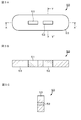
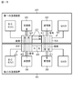
- FIG. 1 is a plan view including a partial cross section showing a basic configuration of a communication system according to an embodiment of the present disclosure.
- FIG. 2A is a block diagram illustrating an example of a specific configuration of the transmission unit
- FIG. 2B is a block diagram illustrating an example of a specific configuration of the reception unit.
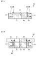
- 3A is a top view illustrating the first connector portion according to the first embodiment
- FIG. 3B is a cross-sectional view taken along the line XX ′ of FIG. 3A
- FIG. 3C is a cross-sectional view of FIG.
- FIG. 6 is a cross-sectional view taken along line YY ′.
- 4A is a top view illustrating a second connector portion according to the first embodiment
- FIG. 4B is a cross-sectional view taken along the line XX ′ of FIG. 4A
- FIG. 4C is a cross-sectional view of FIG.
- FIG. 6 is a cross-sectional view taken along line YY ′.
- FIG. 5A is a diagram illustrating a state in which magnetic lines of force concentrate on a coupling portion between the second connector portion and the first connector portion
- FIG. 5B illustrates a coupling state of the second connector portion with respect to the first connector portion. It is sectional drawing shown.
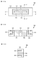
- FIG. 6 is a cross-sectional view illustrating the first connector portion and the second connector portion before coupling in the connector device according to the second embodiment.
- FIG. 5A is a diagram illustrating a state in which magnetic lines of force concentrate on a coupling portion between the second connector portion and the first connector portion
- FIG. 5B illustrates a coupling state of the second connector portion with respect to the first connector portion. It is sectional drawing shown.
- FIG. 6 is a cross-
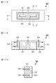
- FIG. 7 is a cross-sectional view illustrating the first connector portion and the second connector portion before being coupled in the connector device according to the third embodiment.
- 8A is a top view illustrating a first connector portion according to the fourth embodiment
- FIG. 8B is a cross-sectional view taken along the line XX ′ in FIG. 8A
- FIG. 8C is a cross-sectional view of FIG.
- FIG. 6 is a cross-sectional view taken along line YY ′.
- 9A is a top view illustrating a second connector portion according to the fourth embodiment
- FIG. 9B is a cross-sectional view taken along line XX ′ of FIG. 9A
- FIG. 9C is a cross-sectional view of FIG. 9A.
- FIG. 9A is a top view illustrating a second connector portion according to the fourth embodiment
- FIG. 9B is a cross-sectional view taken along line XX ′ of FIG. 9A
- FIG. 9C is a cross-sectional
- FIG. 6 is a cross-sectional view taken along line YY ′.
- 10A is a top view illustrating a first connector portion according to the fifth embodiment
- FIG. 10B is a cross-sectional view taken along the line XX ′ of FIG. 10A
- FIG. 10C is a cross-sectional view of FIG.
- FIG. 6 is a cross-sectional view taken along line YY ′.
- 11A is a top view illustrating a second connector portion according to the fifth embodiment
- FIG. 11B is a cross-sectional view taken along the line XX ′ in FIG. 11A
- FIG. 11C is a cross-sectional view of FIG.
- FIG. 6 is a cross-sectional view taken along line YY ′.
- FIG. 12A is a top view illustrating the first connector unit 50 according to the sixth embodiment, and FIG. 12B is a cross-sectional view taken along line X-X ′ in FIG. 12A.
- FIG. 13A is a top view illustrating the second connector unit 60 according to the sixth embodiment, and FIG. 13B is a cross-sectional view taken along line X-X ′ in FIG. 13A.
- FIG. 14 is a schematic diagram illustrating the configuration of the connector device according to the seventh embodiment.
- FIG. 15 is a schematic diagram illustrating the configuration of the connector device according to the eighth embodiment.
- FIG. 16 is a schematic diagram illustrating the configuration of the connector device according to the ninth embodiment.
- FIG. 17A is a diagram illustrating a relationship between a waveguide and an annular groove when a waveguide has a horizontally long rectangular shape
- FIG. 17B illustrates a waveguide and a circular shape when a waveguide has a vertically long rectangular shape. It is a figure which shows the relationship with a groove
- FIG. 18 is a schematic diagram illustrating the configuration of the connector device according to the tenth embodiment.
- FIG. 19 is a schematic diagram illustrating the configuration of the connector device according to the eleventh embodiment.
- FIG. 20 is a schematic diagram illustrating the configuration of the connector device according to the twelfth embodiment.
- Example 2 (Modification of Example 1) 3-3.
- Example 3 (another modification of Example 1) 3-4.
- Example 4 (another modification of Example 1) 3-5.
- Example 5 (an example in which both the electronic device side and the peripheral device side include magnets) 3-6.
- Example 6 (equipped with a power connector) 3-7.
- Example 7 (Modification of Example 6) 3-8.
- Example 8 (Modification of Example 7) 3-9.
- Example 9 (Example having a choke structure for suppressing unwanted radiation) 3-10.
- Example 10 (Example in which the attractive force is improved by changing the arrangement of the magnet and the yoke) 3-11.
- Example 11 (modified example of Example 10) 3-12.
- Example 12 (Example of structure capable of reverse insertion) 4). Modified example
- the second connector portion includes a shield member made of a rubber-like elastic body provided between the yoke and the magnet so as to protrude from the end surface of the yoke and the magnet. It can be configured. Moreover, it can be set as the structure covered with the shielding material which consists of a magnetic body about the waveguide of a 1st connector part.
- the first connector portion may have a configuration in which a part of the yoke is provided so as to cover the periphery of the magnet.
- the first connector portion is provided so that the magnet surrounds the periphery of the yoke, and the shield member is formed of a rubber-like elastic body between the yoke and the magnet. It can be set as the structure which has these. At this time, it can be set as the structure provided in the state which does not protrude from the end surface of a yoke and a magnet about a shield member.
- the first connector unit and the second connector unit may include a power supply terminal that supplies power between the two.
- the shield material of the first connector part and the yoke of the second connector part can also be configured to serve as a power supply terminal that supplies power between the first connector part and the second connector part. .
- a groove is provided around the waveguide in an annular shape with respect to at least one yoke of the first connector portion and the second connector portion. It can be set as the structure which has the chalk structure comprised. At this time, the depth of the groove of the choke structure is preferably set to 1 ⁇ 4 of the wavelength of the high frequency signal.
- the first connector portion two waveguides, two yokes covering each of the two waveguides, an intermediate yoke provided between the two yokes, and A structure having a coupling yoke for magnetically coupling the two yokes and the intermediate yoke can be adopted.
- the second connector part two waveguides corresponding to the two waveguides of the first connector part, two yokes covering each of the two waveguides, and an intermediate yoke of the first connector part
- the attracting portion of the second connector portion is composed of a magnet provided between two yokes and a yoke for magnetically coupling each of the two yokes to the magnet, or alternatively composed of a yoke. It can be configured.
- the connector device and the communication system for the first connector portion, three waveguides, three yokes covering each of the three waveguides, and three yokes are magnetically coupled. It is possible to use a configuration in which an intermediate waveguide of the three waveguides is used for reception or transmission, and one of the waveguides at both ends is used for transmission or reception.
- the second connector part three waveguides corresponding to the three waveguides of the first connector part, three yokes covering each of the three waveguides, and 2 provided between the three yokes It can be set as the structure which has two magnets.
- the second connector portion uses the intermediate waveguide of the three waveguides for transmission and both the waveguides for reception. It can be set as the structure used as.
- the first connector unit uses the intermediate waveguide for transmission
- the second connector unit uses the intermediate waveguide of the three three waveguides for reception and the waveguides at both ends. Both can be configured to be used for transmission.
- the other of the waveguides at both ends of the first connector portion preferably has a termination structure in which the side opposite to the side coupled to the second connector portion is closed.
- a high frequency signal can be a millimeter wave band signal.
- the communication form is communication using a millimeter wave band signal as a high frequency signal, so-called millimeter wave communication, and has the following advantages. a) Since the millimeter wave communication can take a wide communication band, it is easy to increase the data rate. b) The frequency used for transmission can be separated from the frequency of other baseband signal processing, and interference between the millimeter wave and the frequency of the baseband signal hardly occurs. c) Since the millimeter wave band has a short wavelength, the coupling structure and the waveguide structure determined according to the wavelength can be reduced.
- the stability of a carrier wave has strict regulations to prevent interference and the like.
- a highly stable external frequency reference component, a multiplier circuit, a PLL (phase locked loop circuit), and the like are used, and the circuit scale increases.
- a carrier with low stability can be used for transmission, and an increase in circuit scale can be suppressed. Can do.
- FIG. 1 is a plan view including a partial cross section showing a basic configuration of a communication system to which the technology of the present disclosure is applied.
- the communication system 10 according to this application example is between two electronic devices (hereinafter referred to as “communication devices”), specifically, between the first communication device 20 and the second communication device 30. In this configuration, signal transmission (communication) is performed through a high-speed transmission path.
- the first communication device 20 has a configuration in which a transmitter 22 and a waveguide 23 are housed in a housing 21.
- the second communication device 30 has a configuration in which the receiving unit 32 and the waveguide 33 are housed in the housing 31.
- the casing 21 of the first communication device 20 and the casing 31 of the second communication device 30 have a rectangular shape, for example, and are a dielectric, for example, a dielectric constant of about 3 and a thickness of about 0.2 [mm].
- the communication system 10 including the first communication device 20 and the second communication device 30 performs communication between the communication devices 20 and 30 using a high-frequency signal, for example, a millimeter-wave band signal, via the connector device 40. Do. That is, the connector device 40 performs an electrical connection between the first communication device 20 and the second communication device 30.
- the connector device 40 includes a first connector portion 24 on the first communication device 20 side and a second connector portion 34 on the second communication device 30 side.
- a waveguide that forms a transmission path for transmitting a millimeter-wave band signal transmitted from the transmission unit 22 between the output end of the transmission unit 22 and the first connector unit 24. 23 is provided.
- a waveguide 33 that forms a transmission path for transmitting a millimeter-wave band signal to be received is provided between the input end of the receiving unit 32 and the second connector unit 34. Is provided.
- Examples of the types of waveguides include hollow waveguides and dielectric waveguides.
- a hollow waveguide in particular, a rectangular waveguide having a rectangular cross section is used.
- a waveguide having a dimensional ratio of 2: 1 between the long side and the short side of the cross section is preferable.
- the 2: 1 rectangular waveguide has the advantage of preventing high-order modes from occurring and transmitting efficiently.
- the waveguides 23 and 33 do not exclude the use of a waveguide whose cross-sectional shape is other than rectangular, for example, a waveguide whose cross-sectional shape is square or circular.
- the transmission unit 22 converts the signal to be transmitted into a millimeter-wave band signal and outputs the signal to the waveguide 23.
- the waveguide 23 transmits the millimeter waveband signal output from the transmission unit 22 to the second communication device 30 via the connector device 40.
- the reception unit 32 receives a millimeter-wave band signal transmitted from the first communication device 20 side through the connector device 40 and the waveguide 33, and returns the signal to the original transmission target signal. Perform (restore) processing.
- FIG. 2A illustrates an example of a specific configuration of the transmission unit 22
- FIG. 2B illustrates an example of a specific configuration of the reception unit 32.
- the transmission unit 22 includes, for example, a signal generation unit 221 that processes a signal to be transmitted to generate a millimeter-wave band signal.
- the signal generation unit 221 is a signal conversion unit that converts a signal to be transmitted into a millimeter waveband signal, and includes, for example, an ASK (Amplitude Shift Keying) modulation circuit. Specifically, the signal generation unit 221 generates a millimeter-wave band ASK modulated wave by multiplying the millimeter-wave band signal supplied from the oscillator 222 and the transmission target signal by the multiplier 223, and sets the buffer 224. Output.
- ASK Amplitude Shift Keying
- a connector device 25 is interposed between the transmitter 22 and the waveguide 23.
- the connector device 25 couples the transmission unit 22 and the waveguide 23 by, for example, capacitive coupling, electromagnetic induction coupling, electromagnetic field coupling, resonator coupling, or the like.
- the waveguide 23 is provided between the connector device 25 and the first connector portion 24.
- the receiving unit 32 includes, for example, a signal restoring unit 321 that processes a millimeter waveband signal given through the waveguide 33 and restores the original transmission target signal.
- the signal restoration unit 321 is a signal conversion unit that converts a received millimeter-wave band signal into an original signal to be transmitted, and includes, for example, a square (square) detection circuit. Specifically, the signal restoration unit 321 converts the millimeter waveband signal (ASK modulated wave) given through the buffer 322 into the original transmission target signal by squaring with the multiplier 323, and outputs the signal through the buffer 324. It has a configuration.
- a connector device 35 is interposed between the waveguide 33 and the receiving unit 32.
- the connector device 35 couples the waveguide 33 and the receiving unit 32 by, for example, capacitive coupling, electromagnetic induction coupling, electromagnetic field coupling, resonator coupling, or the like.
- the waveguide 33 is provided between the second connector portion 34 and the connector device 35.
- the communication system 10 uses a millimeter-wave band signal as a high-frequency signal between the first communication device 20 and the second communication device 30.
- This is millimeter wave communication in which communication is performed via the connector device 40.
- the first communication device 20 is composed of an electronic device, for example, a portable terminal device such as a notebook personal computer, a tablet, or a smartphone
- the second communication device 30 is a peripheral device of the electronic device,
- a system configuration including a stand-type expansion device called a cradle can be exemplified.
- the system configuration illustrated here is an example, and the present invention is not limited to this.
- the communication system 10 having the above-described configuration that is, the communication system 10 that performs communication using a high-frequency signal, preferably a millimeter-wave band signal, increases the strength against electrical breakdown while maintaining physical strength. This is made in order to realize a connector device 40 that is resistant to general destruction.
- the connector apparatus 40 which concerns on this embodiment is the 1st connector corresponded to the 1st connector part 24 of FIG. 1 provided in the 1st communication apparatus 20 side, as shown in FIG.3 and FIG.4. Part 50 and a second connector part 60 corresponding to the second connector part 34 of FIG. 1 provided on the second communication device 30 side.
- each of the first connector unit 50 and the second connector unit 60 is a waveguide (waveguide) that transmits a millimeter-wave band signal that is an example of a high-frequency signal (high-speed signal).
- a millimeter-wave band signal is transmitted by electromagnetic coupling instead of current. Therefore, even if the connecting portion between the first connector portion 50 and the second connector portion 60 of the connector device 40 is not completely in contact, that is, there is a gap between them, or the reliability of the joint portion is high. Even if it is bad, the influence on the transmission of millimeter-wave signals is small.
- the second connector portion 60 includes a waveguide that transmits a millimeter-wave band signal, a yoke provided to cover the waveguide, and a magnet that forms a magnetic circuit with the yoke.
- the first connector portion 50 can be coupled by the magnet's attractive force.
- a through-hole in the signal transmission direction is formed in the yoke, and a millimeter-wave band signal is transmitted using the through-hole as a waveguide (waveguide).
- the second connector portion 60 can be coupled to the first connector portion 50 by the magnet's attractive force, and is weak against physical destruction. That is, there is no insertion / extraction portion with a weak physical strength in the joint portion. Moreover, it is a coupling structure by a combination of a magnet and a yoke. Accordingly, since the number of parts is small, the connector device 40 can be downsized. In particular, by using a high-frequency signal such as a millimeter wave band as a high-frequency signal (high-speed signal), the waveguide size (yoke size) can be reduced, so the connector device 40 can be further downsized. Is possible.
- the coupling structure is a combination of a magnet and a yoke, it is easy to attach / detach (attach / remove) the second connector part 60 to / from the first connector part 50, and the first connector part 50 and the second connector part
- the connector portion 60 can be securely coupled. Therefore, according to the connector device 40 according to the present embodiment, it is possible to increase the strength against physical breakdown while increasing the strength against electrical breakdown.
- the magnetic flux passes through the waveguide, it is possible to reliably perform alignment between the waveguides of both the first connector portion 50 and the second connector portion 60, or to guide both of them.
- the positional deviation of the waveguide can be minimized. Incidentally, in the case of a waveguide (a structure in which a waveguide and a magnet are separately provided), the positional deviation (tolerance) becomes larger than that in the case of an integrated structure.
- each of the first connector unit 50 and the second connector unit 60 has two waveguides in order to realize bidirectional communication.
- the first connector unit 50 is a connector unit on the electronic device side such as a notebook personal computer, a tablet, or a smartphone
- the second connector unit 60 is a cradle or the like.
- the case of the peripheral device side connector portion will be described as an example.
- Example 1 3A is a top view illustrating the first connector unit 50 according to the first embodiment, FIG. 3B is a cross-sectional view taken along the line XX ′ of FIG. 3A, and FIG. 3C is a cross-sectional view of FIG. FIG. 6 is a cross-sectional view taken along line YY ′.
- the first connector unit 50 includes, for example, two millimeter wave waveguides (millimeter wave waveguides) 51 and 52.
- the millimeter wave waveguides 51 and 52 are made of a dielectric, for example.
- the two millimeter wave waveguides 51 and 52 are covered with a millimeter wave shield material 53 made of a magnetic material such as 400 series (chromium) stainless steel.
- the millimeter wave shield material 53 has a structure integrated with the dielectric waveguide including the millimeter wave waveguides 51 and 52.
- 400 series stainless steel is a ferromagnetic material.
- FIG. 4A is a top view showing the second connector portion 60 according to the first embodiment
- FIG. 4B is a cross-sectional view taken along the line XX ′ of FIG. 4A
- FIG. 4C is a cross-sectional view of FIG.
- FIG. 6 is a cross-sectional view taken along line YY ′.
- the second connector section 60 has two millimeter wave waveguides 61 and 62 corresponding to the millimeter wave waveguides 51 and 52 of the first connector section 50.
- the millimeter wave waveguides 61 and 62 are covered with, for example, a flange-shaped yoke 63 made of a magnetic material such as 400 series stainless steel.
- the yoke 63 has a structure integrated with the dielectric waveguide including the millimeter wave waveguides 61 and 62.
- the yoke 63 also serves as a millimeter wave shield material.
- a magnet 64 having a rectangular annular shape is disposed on the flange portion of the yoke 63.
- an anisotropic magnet having a feature of strongly magnetizing only in a specific direction can be used.
- the magnet 64 has a vertical arrangement in which the S pole and the N pole are arranged in the direction of transmitting the millimeter wave band signals of the millimeter wave waveguides 61 and 62, so that the magnet 64 and the yoke 63 together with the magnetic field lines.
- a magnetic circuit that is a path of magnetic flux that is a bundle is formed.
- the magnet 64 is not limited to the vertical arrangement example of the S pole and the N pole, and may be a horizontal arrangement example in which the S pole and the N pole are arranged inside and outside the rectangular ring.
- the magnet 64 may be arranged so long as it can form a magnetic circuit together with the yoke 63.
- a shield member 65 made of a rubber-like elastic body such as a carbon-based conductive rubber material is provided between the yoke 63 and the magnet 64 so as to surround the yoke 63. As shown in FIGS. 4B and 4C, the shield member 65 is provided in a state of protruding from the end surfaces of the yoke 63 and the magnet 64.
- the shield member 65 functions as a shield material for preventing leakage of millimeter wave band signals to the outside, and also serves to prevent a short circuit between the S pole and the N pole of the magnet 64.
- the connector device 40 according to the first embodiment including the first connector portion 50 and the second connector portion 60 having the above-described configuration
- the first connector portion 50 is brought into contact with the first connector portion 50 by the attractive force of the magnet 64 that forms a magnetic circuit together with the yoke 63.
- the 2nd connector part 60 couple
- the connector device 40 according to the first embodiment has a structure in which the shield material (yoke 63) serving as a guide for the millimeter wave waveguides 61 and 62 and the magnetic circuit are integrated in the second connector portion 60. There is no connector insertion / removal part, and it is difficult to be physically damaged. In addition, since there is no insertion / removal portion weak in physical strength at the coupling portion, the connector device 40 can be reduced in size and thickness.
- the magnetic force line of the magnet 64 is shown in the connection surface (contact surface) with the 1st connector part 50, as shown to FIG. 5A. Since they can be concentrated, the attractive force of the yoke 63 based on the magnetic lines of force of the magnet 64 can be increased. As a result, it is possible to compensate for a decrease in the attractive force due to a decrease in the area of the magnetic force generation surface, which is a disadvantage of the connector device 40 being reduced in size and thickness.
- the first connector can be obtained with a sufficient suction force.
- the second connector part 60 can be coupled to the part 50.
- the second connector portion 60 is coupled to the first connector portion 50, as shown in FIG. 5B, the projecting portion of the shield member 65 is crushed and the millimeter wave of the first connector portion 50 is collapsed.
- the distance between the shield material 53 is reduced, and the gap between the millimeter wave shield material 53 is filled.
- the magnetic field lines in the coupling portion are strengthened, the attractive force of the yoke 63 based on the magnetic field lines of the magnet 64 is increased, and the millimeter wave waveguides 51 and 52 on the first connector unit 50 side and the second connector unit 60 side Leakage of radio waves between the millimeter wave waveguides 61 and 62 can be prevented.
- the data communication in the millimeter wave band using the connector device 40 according to the first embodiment is, for example, about 5 G [bps] in a process of 40 [nm] per channel. Is possible.
- the connector device 40 according to the first embodiment has a structure that prevents radio wave leakage between the first connector unit 50 and the second connector unit 60, and therefore, by repeating the same structure as the connector structure. It is possible to increase the bandwidth by providing a plurality of waveguides. Similarly, full-duplex bidirectional communication can also be performed by allocating the transmission side and the reception side to each of a plurality of waveguides.
- FIG. 6 is a cross-sectional view illustrating the first connector portion 50 and the second connector portion 60 before being coupled in the connector device 40 according to the second embodiment.
- the first connector unit 50 is directly attached to the millimeter wave module 71 on the transmission side, and the millimeter wave module 72 on the reception side is connected to the second connector unit 60. It has a configuration directly attached to.
- the millimeter wave module 71 on the transmission side is configured to include the transmission unit 22 and the like shown in FIG.
- the receiving-side millimeter wave module 72 includes the receiving unit 32 and the like shown in FIG. 2B. For example, it is electrically connected to a main board (not shown) via a flexible cable 74.
- FIG. 7 is a cross-sectional view illustrating the first connector portion 50 and the second connector portion 60 before being coupled in the connector device 40 according to the third embodiment.
- the connector device 40 connects the first connector unit 50 to the transmitting-side millimeter wave module 71 via the waveguides 75 and 76, and the second connector unit. 60 is connected to the receiving-side millimeter-wave module 72 via waveguides 77 and 78.
- the transmission-side millimeter wave module 71 and the reception-side millimeter wave module 72 are each mounted on a main board (not shown).
- the waveguides 75 and 76 are shielded waveguides covered with shield members 79 and 80, and are integrated with the waveguides 51 and 52 of the first connector unit 50.
- a conductive plastic member 81 is provided at a connection portion between the shielded waveguides 75 and 76 and the first connector portion 50.
- the waveguides 77 and 78 are shielded waveguides covered with the shield members 82 and 83, and are integrated with the waveguides 61 and 62 of the second connector unit 60.
- a conductive plastic member 84 is provided at a connection portion between the shielded waveguides 77 and 78 and the second connector portion 60.
- the fourth embodiment is a further modification of the first embodiment, and has a structure in which the suction force is further increased than that of the first embodiment.
- FIG. 8A is a top view illustrating the first connector unit 50 according to the fourth embodiment
- FIG. 8B is a cross-sectional view taken along the line XX ′ of FIG. 8A
- FIG. 8C is a cross-sectional view of FIG.
- FIG. 6 is a cross-sectional view taken along line YY ′.
- the first connector unit 50 according to the fourth embodiment has basically the same configuration as the first connector unit 50 according to the first embodiment. That is, the first connector unit 50 according to the fourth embodiment includes two millimeter wave waveguides 51 and 52 made of, for example, a dielectric, and the millimeter wave waveguides 51 and 52 are made of a magnetic material such as 400 series stainless steel. The structure is covered with the wave shield material 53. The only difference from the first connector portion 50 according to the first embodiment is that the surface area of the millimeter wave shield material 53 covering the millimeter wave waveguides 51 and 52 is larger than that in the first embodiment.
- FIG. 9A is a top view showing the second connector unit 60 according to the fourth embodiment
- FIG. 9B is a cross-sectional view taken along the line XX ′ of FIG. 9A
- FIG. 9C is a cross-sectional view of FIG. FIG. 6 is a cross-sectional view taken along line YY ′.
- the second connector unit 60 according to the fourth embodiment has basically the same configuration as the second connector unit 60 according to the first embodiment. That is, the second connector unit 60 according to the fourth embodiment includes two millimeter wave waveguides 61 and 62 corresponding to the millimeter wave waveguides 51 and 52 of the first connector unit 50, and these millimeter wave waveguides 61 and 62. Is covered with, for example, a flange-shaped yoke 63 made of a magnetic material such as 400 series stainless steel. A magnet 64 having, for example, a rectangular annular shape is disposed on the flange portion of the yoke 63.
- a shield member 65 made of a rubber-like elastic body such as a carbon-based conductive rubber material surrounds the yoke 63, and part of the yoke 63 and the magnet 64 are included. It is provided in a state of protruding from the end face of.
- the yoke 63 has a flange portion extending outside the magnet 64 and the outermost peripheral portion standing up, so that a portion 63A of the yoke 63 is provided.
- a part (outer peripheral part) 63A of the yoke 63 has a yoke structure that covers the outer periphery of the magnet 64, so that a part 63A of the yoke 63 does not have a yoke structure that covers the outer periphery of the magnet 64.
- the suction force of the second connector portion 60 with respect to the first connector portion 50 can be further increased.
- the connector device 40 according to the first embodiment is an example in which only the connector portion (second connector portion 60) on the peripheral device side includes a magnet, whereas the connector device 40 according to the fifth embodiment is an electronic device. This is an example in which both the connector portions on the side and the peripheral device side are provided with magnets.
- FIG. 10A is a top view illustrating the first connector unit 50 according to the fifth embodiment
- FIG. 10B is a cross-sectional view taken along line XX ′ of FIG. 10A
- FIG. 10C is a cross-sectional view of FIG.
- FIG. 6 is a cross-sectional view taken along line YY ′.
- the first connector unit 50 according to the fifth embodiment has basically the same configuration as the second connector unit 60 according to the first embodiment. That is, the first connector unit 50 according to the fifth embodiment includes two millimeter wave waveguides 51 and 52, and the millimeter wave waveguides 51 and 52 are made of a magnetic material such as 400 series stainless steel, for example, a flange-shaped yoke 54. It is the structure covered with. An anisotropic magnet 55 having, for example, a rectangular annular shape is disposed on the flange portion of the yoke 54.
- a shield member 56 made of a rubber-like elastic material such as a carbon-based conductive rubber material is provided between the yoke 54 and the magnet 55 so as to surround the yoke 54.
- the first connector portion 50 is different from the second connector portion 60 according to the first embodiment in that the shield member 56 does not protrude from the end surfaces of the yoke 63 and the magnet 64, that is, from the end surfaces of the yoke 63 and the magnet 64. It is only a point provided with no protrusion.
- the protrusion of the shield member 56 from the end surfaces of the yoke 63 and the magnet 64 is eliminated, the distance between the first connector portion 50 and the second connector portion 60 in the coupled state has a protrusion. Can be close compared to.
- FIG. 11A is a top view showing the second connector portion 60 according to the fifth embodiment
- FIG. 11B is a cross-sectional view taken along the line XX ′ in FIG. 11A
- FIG. FIG. 6 is a cross-sectional view taken along line YY ′.
- the second connector unit 60 according to the fifth embodiment has the same configuration as the second connector unit 60 according to the first embodiment. That is, the second connector unit 60 according to the fifth embodiment includes two millimeter wave waveguides 61 and 62 corresponding to the millimeter wave waveguides 51 and 52 of the first connector unit 50, and these millimeter wave waveguides 61 and 62. Is covered with, for example, a flange-shaped yoke 63 made of a magnetic material such as 400 series stainless steel. A magnet 64 having, for example, a rectangular annular shape is disposed on the flange portion of the yoke 63.
- a shield member 65 made of a rubber-like elastic body such as a carbon-based conductive rubber material surrounds the yoke 63, and part of the yoke 63 and the magnet 64 are included. It is provided in a state of protruding from the end face of.
- the magnet 55 on the first connector unit 50 side and the magnet on the second connector unit 60 side are provided so that different magnetic poles face each other. Thereby, the attraction
- the distance between the first connector portion 50 and the second connector portion 60 in the coupled state is reduced by eliminating the protrusion of the shield member 65 on the first connector portion 50 side.
- the protrusion of the shield member 65 on the second connector portion 60 side may be eliminated.
- the shield structure of the fourth embodiment that is, the shield structure in which a part of the yoke 63 covers the outer periphery of the magnet 64 can be applied.
- the connector device 40 according to the sixth embodiment is configured to integrally include a power supply connector based on, for example, the configurations of the first connector portion 50 and the second connector portion 60 according to the first embodiment.
- FIG. 12A is a top view showing the first connector unit 50 according to the sixth embodiment
- FIG. 12B is a cross-sectional view taken along the line X-X ′ of FIG. 12A.
- the first connector unit 50 according to the sixth embodiment is a constituent element of the first connector unit 50 according to the first embodiment that is a base, that is, two millimeter wave waveguides 51 and 52 and a millimeter wave shield material 53 covering them. However, it is configured to be fitted into the through hole 57A in the center of the insulating base 57 such as plastic.
- power supply terminals for example, jacks
- 58A and 58B for supplying power between the first connector portion 50 and the second connector portion 60 are provided on the convex portions 57B and 57C at both ends in the longitudinal direction of the base 57. Is provided.
- FIG. 13A is a top view showing the second connector portion 60 according to the sixth embodiment
- FIG. 13B is a cross-sectional view taken along line X-X ′ in FIG. 13A.
- the second connector portion 60 according to the sixth embodiment is a constituent element of the second connector portion 60 according to the first embodiment that is a base, that is, two millimeter wave waveguides 61 and 62, a yoke 63, a magnet 64, and the like. However, it is configured to be fitted into the through hole 66A in the center of the insulating base 66 such as plastic.
- Power supply terminals for example, plugs
- 67A and 67B for supplying power between the first connector part 50 and the second connector part 60 are provided at both ends of the base body 66 in the longitudinal direction.
- annular mounting portions 66B and 66C that are elastically detachable with respect to the convex portions 57B and 57C of the base 57 in the first connector portion 50 are provided.
- the power terminals 58A and 58B on the first connector portion 50 side and the second connector portion 60 are connected.
- a power connector is constituted by the power terminals 67A and 67B.
- the case where the configurations of the first connector portion 50 and the second connector portion 60 according to the first embodiment are used as a base has been described as an example.
- the configuration of the first connector unit 50 and the second connector unit 60 may be used as a base.
- the technique of the present embodiment can be applied to the connector device 40 according to the second to fifth embodiments.
- the seventh embodiment is a modification of the sixth embodiment.
- a configuration is adopted in which the magnetic poles are arranged such that the S pole and the N pole of the magnet 64 are aligned in the signal transmission direction of the millimeter wave waveguides 61 and 62 (direction in which millimeter wave band signals are transmitted). It was.
- the magnetic pole arrangement is such that the south pole and the north pole of the magnet 64 are arranged in a direction orthogonal to the signal transmission direction.
- FIG. 14 is a schematic diagram illustrating the configuration of the connector device 40 according to the seventh embodiment.
- the first communication device 20 has a reception unit 26 in addition to the transmission unit 22, and the second communication device 30 is added to the reception unit 32.
- the transmission unit 36 is included.
- the receiving unit 26 of the first communication device 20 the same configuration as the receiving unit 32 of the second communication device 30 can be used.
- the transmission unit 36 of the second communication device 30 the same configuration as that of the transmission unit 22 of the first communication device 20 can be used.
- the inside of the waveguides 51 and 52 and the waveguides 61 and 62 A magnetic circuit through which the magnetic flux passes can be formed.
- the magnetic flux passes through the waveguides 51 and 52 and the waveguides 61 and 62, between the waveguides 51, 52/61 and 62 of both the first connector unit 50 and the second connector unit 60.
- the alignment can be performed reliably, or the positional deviation between the two waveguides 51, 52/61, 62 can be minimized.
- millimeter waveband signals are transmitted from the transmission unit 22 to the reception unit 32 through the waveguide 51 and the waveguide 61 between the first communication device 20 and the second communication device 30. Then, millimeter wave band signals are transmitted from the transmission unit 36 to the reception unit 26 through the waveguide 62 and the waveguide 52. That is, bidirectional communication is performed between the first communication device 20 and the second communication device 30. Also, for example, DC5 [V] power is transmitted between the power terminal 58A on the first connector section 50 side and the power terminal 67A of the second connector section 60, and the power terminal 58B and the power terminal 67B are transmitted. The ground potential (GND) is transmitted between the two.
- DC5 [V] power is transmitted between the power terminal 58A on the first connector section 50 side and the power terminal 67A of the second connector section 60, and the power terminal 58B and the power terminal 67B are transmitted.
- the ground potential (GND) is transmitted between the two.
- Example 8 The eighth embodiment is a modification of the seventh embodiment.
- the millimeter-wave shield 53 and the yoke 63 that also serve as a waveguide (waveguide) can transmit millimeter-wave band signals through the waveguides 51 and 52 and the waveguides 61 and 62, and can also pass a DC current. Is possible.
- Example 8 was made paying attention to this point.
- FIG. 15 is a schematic diagram illustrating the configuration of the connector device 40 according to the eighth embodiment.
- the connector device 40 according to the eighth embodiment has a configuration in which the millimeter wave shield material 53 and the yoke 63 are also used as power supply terminals.
- the connector device 40 can be reduced in size as compared with the seventh embodiment.
- the waveguide 51 side and the waveguide 52 side of the millimeter wave shield material 53 are separated by the insulating material 27 on the first communication device 20 side. Must be electrically isolated.
- the millimeter-wave shield 53 and the yoke 63 that also serve as a waveguide can transmit a millimeter-wave band signal, which is a high-speed signal, and can also flow a DC current. Accordingly, since the millimeter wave shield material 53 and the yoke 63 are also used as the power supply terminals and the power supply voltage (DC5 [V] in this example) is superposed, a dedicated power supply terminal becomes unnecessary. It is possible to reduce the size and the number of parts.
- the connector device 40 according to the ninth embodiment has a configuration in which a choke structure is formed in the millimeter wave shield material 53 that also serves as a waveguide and the yoke 63 to suppress unnecessary radiation (radio wave leakage).
- the basic structure is based on the connector device 40 according to the seventh embodiment shown in FIG.
- FIG. 16 is a schematic diagram illustrating the configuration of the connector device 40 according to the eighth embodiment.
- grooves 59A and 59B are formed in an annular shape (for example, an elliptical annular shape) around the central axis of the waveguides 51 and 52 on the end surface of the millimeter wave shield material 53 facing the yoke 63.
- the annular grooves 59A and 59B form a choke structure 59 on the first connector portion 50 side that suppresses unnecessary radiation (radio wave leakage).
- 17A and 17B show the relationship between the waveguide 51 (52) and the annular groove 59A (59B).
- 17A shows a case where the shape of the waveguide 51 (52) is a horizontally long rectangle
- FIG. 17B shows a case where the shape of the waveguide 51 (52) is a vertically long rectangle.
- the end surface of the yoke 63 on the side facing the millimeter wave shield material 53 is around the central axis of the waveguides 61 and 62.
- Grooves 68A and 68B are formed in an annular shape (for example, an elliptical annular shape). The annular grooves 68A and 68B form a choke structure 68 on the second connector portion 60 side that suppresses unnecessary radiation.
- the depth of the annular grooves 59A and 59B is 1 ⁇ 4 of the wavelength ⁇ of the high frequency (in this example, millimeter wave) transmitted by the waveguides 51 and 52 ( ⁇ / 4) is preferably set.
- the depth of the annular grooves 68A and 68B of the choke structure 68 on the second connector portion 60 side is also preferably set to ⁇ / 4.
- the pitches of the grooves 59A and 59B and the grooves 68A and 68B are preferably set to ⁇ / 4.
- “ ⁇ / 4” means not only strictly ⁇ / 4 but also substantially ⁇ / 4, and the presence of various variations in design or manufacturing is acceptable. Is done.
- the choke structure 59 and the choke structure can be obtained simply by digging the grooves 59A and 59B and the grooves 68A and 68B in the end surfaces (contact surfaces) of the millimeter wave shield material 53 and the yoke 63. 68 can be formed. Accordingly, since a dedicated component (separate component) for suppressing unnecessary radiation is not required, unnecessary radiation can be suppressed while miniaturizing the connector device 40 and reducing the number of components.
- the effect of suppressing unwanted radiation by the choke structures 59 and 68 enables more stable signal transmission even when the reliability of the contact portion between the first connector portion 50 and the second connector portion 60 is poor. Become. Accordingly, even if dust enters between the first connector portion 50 and the second connector portion 60 or a configuration in which a non-metallic sheet such as plastic, glass, or ceramic is sandwiched, the first Signal transmission between the connector part 50 and the second connector part 60 becomes possible.
- the choke structure 59 and the choke structure 68 are provided in both the first connector part 50 and the second connector part 60.
- the first connector part 50 and the second connector part 60 are not provided. It is also possible to adopt a configuration in which only one of them is provided.
- the choke structures 59 and 68 are not limited to those having the above configuration. Specifically, in the above configuration, the configuration in which the number of the grooves 59A and 59B and the grooves 68A and 68B is one (single) is illustrated, but a multi-stage configuration having two or more stages may be used. A larger number of grooves 59A and 59B and grooves 68A and 68B have a greater effect of suppressing unwanted radiation, and transmission of signals is possible even with a thicker non-metallic sheet.
- Embodiments 1 to 8. the technology for suppressing unnecessary radiation (radio wave leakage) by forming a choke structure in the millimeter wave shield material 53 and the yoke 63 that also serve as a waveguide is described in Embodiments 1 to 8. The same applies to the connector device 40.
- the connector device 40 according to the tenth embodiment has a configuration in which the attractive force of the second connector portion 60 with respect to the first connector portion 50 is improved by changing the arrangement of the magnet and the yoke.
- the basic structure is based on the connector device 40 according to the seventh embodiment shown in FIG.
- FIG. 18 is a schematic diagram illustrating the configuration of the connector device 40 according to the tenth embodiment.
- the millimeter wave shield material 53 includes a yoke 53A covering the waveguide 51, a yoke 53B covering the waveguide 52, an intermediate yoke 53C provided between the yoke 53A and the yoke 53B, and a yoke
- the coupling yoke 53D magnetically couples 53A, the yoke 53B, and the intermediate yoke 53C.
- the yoke 63 includes a yoke 63A that covers the waveguide 61, a yoke 63B that covers the waveguide 62, and a yoke 63C that magnetically couples the yoke 63A and the yoke 63B.
- the magnet 64 is arranged at a position facing the intermediate yoke 53C of the first connector unit 50 so that the N pole and the S pole are aligned along the signal transmission direction.
- the magnet 64 and the yoke 63C constitute an attracting portion that generates an attracting force with respect to the intermediate yoke 53C of the first connector portion 50.
- a closed loop of magnetic flux indicated by a broken arrow in FIG. 18 is formed.
- the magnetic flux emitted from the N pole of the magnet 64 passes through the yoke 53C and then branches in the left-right direction in the figure by the yoke 53D to reach the yoke 53A and the yoke 53B. Thereafter, a closed loop of magnetic flux that passes through the yoke 63A and the yoke 63B and returns to the S pole of the magnet 64 through the yoke 63C is formed.
- the connector device 40 according to the tenth embodiment having the configuration described above, not only between the yoke 53A and the yoke 63A and between the yoke 53B and the yoke 63B but also between the intermediate yoke 53C and the magnet 64. Force is generated. Therefore, according to the connector device 40 according to the tenth embodiment, compared with the connector device 40 according to the seventh embodiment in which an attracting force is generated only between the yoke 53A and the yoke 63A and between the yoke 53B and the yoke 63B. Thus, the suction force of the second connector part 60 with respect to the first connector part 50 can be improved.
- FIG. 19 is a schematic diagram illustrating the configuration of the connector device 40 according to the eleventh embodiment.
- the coupling yoke 53D that magnetically couples the yoke 53A, the yoke 53B, and the intermediate yoke 53C includes the yoke 53D- 1 between the yoke 53A and the yoke 53B, the yoke 53B, and the yoke 53C. And the yoke 53D- 2 between them. Then, between the yoke 53D -1 and yoke 53A and the yoke 53C is electrically insulated by an insulating material 27 -1, between the yoke 53D -2 and yoke 53B and the yoke 53C electrically by an insulating material 27 -2 Is insulated.
- an intermediate yoke 63D is provided at an intermediate position between the yoke 63A and the yoke 63B, that is, a position facing the intermediate yoke 53C of the first connector portion 50.
- a magnet 64-1 is arranged between the yoke 63A and the intermediate yoke 63D so that the south pole and the north pole are arranged in a direction orthogonal to the signal transmission direction, and a signal is provided between the yoke 63B and the intermediate yoke 63D.
- the magnet 64-2 is arranged so that the N pole and the S pole are aligned in a direction orthogonal to the transmission direction.
- the magnet 64-1 and the magnet 64-2 are arranged such that the same magnetic poles (in this example, the S poles) face each other.
- the intermediate yoke 63 ⁇ / b> D and the two magnets 64 ⁇ 1 and 64 ⁇ 2 constitute a suction portion that generates a suction force with respect to the intermediate yoke 53 ⁇ / b> C of the first connector portion 50. ing.
- a closed loop of magnetic flux indicated by a broken arrow in FIG. 19 is formed. Specifically, after the magnetic flux from the N pole of the magnet 64 -1 through the yoke 63A and the yoke 53A, the yoke 53D -1, yoke 53C, and, via the yoke 63D to the S pole of the magnet 64 -1 A closed loop of returning magnetic flux is formed.
- the yokes 53A and 63A and the yokes 53B and 63B are also used as power terminals for the ground potential (GND) between the first connector portion 50 and the second connector portion 60.
- 53C and 63D are also used as power terminals for DC5 [V], for example.
- the adsorption force is not only between the yoke 53A and the yoke 63A and between the yoke 53B and the yoke 63B, but also between the yoke 53C and the yoke 63D. Therefore, the suction force of the second connector part 60 with respect to the first connector part 50 can be improved.
- the connector device 40 according to the twelfth embodiment has a configuration in which the second connector portion 60 can be reversely inserted into the first connector portion 50.
- FIG. 20 is a schematic diagram illustrating the configuration of the connector device 40 according to the twelfth embodiment.
- the first connector unit 50 includes three yokes 53A, 53B, 53E that cover each of the three waveguides 51, 52, 91, three waveguides 51, 52, 91, and 3
- the intermediate waveguide 52 of the three waveguides 51, 52, 91 is used for reception, for example, and one of the waveguides 51, 91 at both ends (for example, the waveguide 51) is used for transmission. ing.
- the second connector unit 60 covers each of the three waveguides 61, 62, 92 and the three waveguides 61, 62, 92 corresponding to the three waveguides 51, 52, 91 of the first connector unit 50.
- three yokes 63A, 63B, 63E, and three yokes 63A, 63B, 2 one magnet 64 -1 provided between 63E each other, and a 64 -2.
- the second connector unit 60 uses the intermediate waveguide 62 for transmission and the waveguides 61 and 92 at both ends. Both are configured to be used for reception.
- the second connector portion 50 is second in relation to the first connector portion 50. Even if the connector portion 60 is attached in the opposite direction (so-called reverse insertion), communication is possible.
- reverse direction means a mounting state (state of FIG. 20) in which the transmission waveguide 51 of the first connector unit 50 and the reception waveguide 61 of the second connector unit 60 face each other. In the forward direction, it refers to a mounted state in which the transmission waveguide 51 of the first connector unit 50 and the reception waveguide 92 of the second connector unit 60 face each other.
- the connector device 40 is easy to use. Further, in the first connector portion 50, the waveguide on the unused side, in this example, the waveguide 91, is closed on the opposite side to the side coupled to the second connector portion 60 to form a termination structure. The transmission characteristics can be improved compared to the case where the termination structure is not used.
- the intermediate waveguide 52 is used for reception in the first connector unit 50, but it can also be used for transmission.
- the intermediate waveguide 62 is used for reception and the waveguides 61 and 92 at both ends are used for transmission.
- the technique of this indication is not limited to the said embodiment.
- the configurations and structures of the connector device and the communication system described in the embodiments are merely examples, and can be changed as appropriate.
- the first connector unit 50 and the second connector unit 60 have two waveguides 51, 52/61, and 62, respectively, thereby realizing bidirectional communication as an example.
- the present invention is not limited to application to bidirectional communication. In other words, if it can be applied to single-sided communication, it is possible to increase the number of waveguides to achieve multichanneling. Then, radio wave interference between multi-channels in the case of multi-channel can be prevented by the shield member 65 made of a rubber-like elastic body, the choke structures 59 and 68, and the like.
- this indication can also take the following structures.
- a first connector having a waveguide for transmitting a high-frequency signal;
- a second connector portion comprising: [2]
- the second connector portion includes a shield member made of a rubber-like elastic body provided in a state of protruding from the yoke and the end face of the magnet between the yoke and the magnet.
- the waveguide of the first connector portion is covered with a shield material made of a magnetic material.
- the yoke of the second connector part is provided so that a part thereof covers the periphery of the magnet.
- the first connector portion is provided so that the magnet surrounds the periphery of the yoke, and has a shield member made of a rubber-like elastic body between the yoke and the magnet.
- the shield member of the first connector portion is provided so as not to protrude from the end surfaces of the yoke and the magnet.
- the first connector portion and the second connector portion include a power supply terminal for supplying power between them.
- the shield material of the first connector part and the yoke of the second connector part also serve as a power supply terminal for supplying power between the first connector part and the second connector part.
- At least one yoke of the first connector portion and the second connector portion has a choke structure in which a groove is annularly provided around the waveguide.
- the groove depth of the choke structure is 1/4 of the wavelength of the high frequency signal.
- the first connector portion includes two waveguides, two yokes covering each of the two waveguides, an intermediate yoke provided between the two yokes, and the two yokes and the intermediate yoke. Having a coupling yoke that couples to
- the second connector portion includes two waveguides corresponding to the two waveguides of the first connector portion, two yokes covering each of the two waveguides, and an intermediate yoke of the first connector portion. It has a suction part that generates suction power, The connector device according to [1] above.
- the attracting portion of the second connector portion includes a magnet provided between the two yokes, and a yoke that magnetically couples each of the two yokes to the magnet.
- the connector device includes an intermediate yoke provided between the two yokes, and two magnets provided between the two yokes and the intermediate yoke.
- the connector device according to [11] above.
- the first connector section includes three waveguides, three yokes covering each of the three waveguides, and a coupling yoke that magnetically couples the three yokes.
- the intermediate waveguide is used for reception or transmission, and one of the waveguides at both ends is used for transmission or reception.
- the second connector unit includes three waveguides corresponding to the three waveguides of the first connector unit, three yokes covering each of the three waveguides, and two magnets provided between the three yokes.
- the first connector unit uses the intermediate waveguide for reception
- the second connector unit uses the intermediate waveguide of the three waveguides for transmission, and uses both waveguides for reception.
- the first connector unit uses the intermediate waveguide for transmission
- the second connector unit uses the intermediate waveguide of the three waveguides for reception, and uses both waveguides for transmission.
- the connector device according to [1] above. [15]
- the other of the waveguides at both ends of the first connector portion has a termination structure in which the side opposite to the side coupled to the second connector portion is closed.
- the connector device according to [14] above.
- the high-frequency signal is a millimeter-wave band signal.
- the connector device according to any one of [1] to [15].
- the high-frequency signal is a millimeter-wave band signal.
- the communication system according to [17] above.
Landscapes
- Details Of Connecting Devices For Male And Female Coupling (AREA)
Abstract
本開示のコネクタ装置は、高周波の信号を伝送する導波路を有する第1のコネクタ部と、高周波の信号を伝送する導波路、導波路を覆うように設けられたヨーク、及び、ヨークと磁気回路を形成する磁石を有し、第1のコネクタ部に対して磁石の吸着力によって結合可能な第2のコネクタ部と、を備える。また、本開示の通信システムは、2つの通信装置と、2つの通信装置間において高周波の信号を伝送するコネクタ装置と、を有し、当該コネクタ装置として上記の構成のコネクタ装置を用いる。
Description
本開示は、コネクタ装置及び通信システムに関する。
2つの電子機器(通信装置)間で信号の伝送を行う通信システムでは、コネクタ装置を介して電気的な接続がとられる(例えば、特許文献1参照)。この種の通信システムとして、2つの電子機器の一方が携帯端末装置から成り、他方がクレードルと称されるスタンド型の拡張機器から成る通信システムを例示することができる。但し、この通信システムとしては一例であり、これに限られるものではない。
特許文献1に記載の通信システムでは、高速伝送路を導波路で接続する手法をとっており、当該手法は電気的な破壊に対しての強度向上の観点からは有効である。しかし、電気的な接続をとるコネクタ装置に関しては、プラグとレセプタクルとの組合せから成る、所謂プラグ型の構成となっているため、抜き差し時に物理的な破壊が生じ易い、即ち、物理的な破壊に対して弱いという問題がある。
そこで、本開示は、電気的な破壊に対して強度を上げつつ、物理的な破壊に対して強いコネクタ装置、及び、2つの電子機器間で当該コネクタ装置を介して電気的な接続をとる通信システムを提供することを目的とする。
上記の目的を達成するための本開示のコネクタ装置は、
高周波の信号を伝送する導波路を有する第1のコネクタ部と、
高周波の信号を伝送する導波路、導波路を覆うように設けられたヨーク、及び、ヨークと磁気回路を形成する磁石を有し、第1のコネクタ部に対して磁石の吸着力によって結合可能な第2のコネクタ部と、
を備えるコネクタ装置である。
高周波の信号を伝送する導波路を有する第1のコネクタ部と、
高周波の信号を伝送する導波路、導波路を覆うように設けられたヨーク、及び、ヨークと磁気回路を形成する磁石を有し、第1のコネクタ部に対して磁石の吸着力によって結合可能な第2のコネクタ部と、
を備えるコネクタ装置である。
上記の目的を達成するための本開示の通信システムは、
2つの通信装置と、
2つの通信装置間において高周波の信号を伝送するコネクタ装置と、を有し、
コネクタ装置は、
高周波の信号を伝送する導波路を有する第1のコネクタ部と、
高周波の信号を伝送する導波路、導波路を覆うように設けられたヨーク、及び、ヨークと磁気回路を形成する磁石を有し、第1のコネクタ部に対して磁石の吸着力によって結合可能な第2のコネクタ部と、を備える、
通信システムである。
2つの通信装置と、
2つの通信装置間において高周波の信号を伝送するコネクタ装置と、を有し、
コネクタ装置は、
高周波の信号を伝送する導波路を有する第1のコネクタ部と、
高周波の信号を伝送する導波路、導波路を覆うように設けられたヨーク、及び、ヨークと磁気回路を形成する磁石を有し、第1のコネクタ部に対して磁石の吸着力によって結合可能な第2のコネクタ部と、を備える、
通信システムである。
上記の構成のコネクタ装置、あるいは、通信システムにおいて、第2のコネクタ部は、第1のコネクタ部に対してヨークの吸着力によって結合可能であり、物理的な破壊に対して弱い、即ち、物理的な強度が弱い抜き差し部分が結合部に存在しない。また、磁石及びヨークの組合せによる結合構造であるため、小型化を実現しつつ、第1のコネクタ部に対する第2のコネクタ部の着脱(取り付け/取り外し)が容易で、且つ、第1のコネクタ部と第2のコネクタ部とを確実に結合できる。
本開示によれば、物理的な強度が弱い抜き差し部分が結合部に存在しないとともに、磁石の吸着力によってより確実な結合状態が得られるため、電気的な破壊に対して強度を上げつつ、物理的な破壊に対しての強度を上げることができる。
尚、ここに記載された効果に必ずしも限定されるものではなく、本明細書中に記載されたいずれかの効果であってもよい。また、本明細書に記載された効果はあくまで例示であって、これに限定されるものではなく、また付加的な効果があってもよい。
以下、本開示の技術を実施するための形態(以下、「実施形態」と記述する)について図面を用いて詳細に説明する。本開示の技術は実施形態に限定されるものではなく、実施形態における種々の数値や材料などは例示である。以下の説明において、同一要素又は同一機能を有する要素には同一符号を用いることとし、重複する説明は省略する。尚、説明は以下の順序で行う。
1.本開示のコネクタ装置及び通信システム、全般に関する説明
2.本開示の技術が適用される通信システム
2-1.通信システムの基本的な構成
2-2.送信部及び受信部の具体的な構成
3.本開示の一実施形態に係るコネクタ装置
3-1.実施例1(周辺機器側のみが磁石を備える例)
3-2.実施例2(実施例1の変形例)
3-3.実施例3(実施例1の別の変形例)
3-4.実施例4(実施例1の更に別の変形例)
3-5.実施例5(電子機器側及び周辺機器側の両方が磁石を備える例)
3-6.実施例6(電源用コネクタを一体的に備える)
3-7.実施例7(実施例6の変形例)
3-8.実施例8(実施例7の変形例)
3-9.実施例9(不要輻射を抑制するチョーク構造を有する例)
3-10.実施例10(磁石とヨークの配置を変えて吸着力を向上させた例)
3-11.実施例11(実施例10の変形例)
3-12.実施例12(逆挿し可能な構造の例)
4.変形例
<本開示のコネクタ装置及び通信システム、全般に関する説明>
本開示のコネクタ装置及び通信システムにあっては、第2のコネクタ部について、ヨークと磁石との間にヨーク及び磁石の端面から突出した状態で設けられたゴム状弾性体から成るシールド部材を有する構成とすることができる。また、第1のコネクタ部の導波路について、磁性体から成るシールド材によって覆われている構成とすることができる。
本開示のコネクタ装置及び通信システムにあっては、第2のコネクタ部について、ヨークと磁石との間にヨーク及び磁石の端面から突出した状態で設けられたゴム状弾性体から成るシールド部材を有する構成とすることができる。また、第1のコネクタ部の導波路について、磁性体から成るシールド材によって覆われている構成とすることができる。
上述した好ましい構成を含む本開示のコネクタ装置及び通信システムにあっては、第1のコネクタ部について、ヨークの一部が磁石の周囲を覆うように設けられている構成とすることができる。
また、本開示のコネクタ装置及び通信システムにあっては、第1のコネクタ部について、磁石がヨークの周囲を囲むように設けられおり、ヨークと磁石との間にゴム状弾性体から成るシールド部材を有する構成とすることができる。このとき、シールド部材について、ヨーク及び磁石の端面から突出しない状態で設けられている構成とすることができる。
上述した好ましい構成を含む本開示のコネクタ装置及び通信システムにあっては、第1のコネクタ部及び第2のコネクタ部について、両者間で電源供給を行う電源端子を備える構成とすることができる。あるいは又、第1のコネクタ部のシールド材及び第2のコネクタ部のヨークについて、第1のコネクタ部と第2のコネクタ部との間で電源供給を行う電源端子を兼ねる構成とすることができる。
更に、上述した好ましい構成を含む本開示のコネクタ装置及び通信システムにあっては、第1のコネクタ部及び第2のコネクタ部の少なくとも一方のヨークについて、導波路の周りに溝が環状に設けられて成るチョーク構造を有する構成とすることができる。このとき、チョーク構造の溝の深さについて、高周波の信号の波長の1/4に設定することが好ましい。
本開示のコネクタ装置及び通信システムにあっては、第1のコネクタ部について、2つの導波路、2つの導波路の各々を覆う2つのヨーク、2つのヨーク間に設けられた中間ヨーク、及び、2つのヨークと中間ヨークとを磁気的に結合する結合ヨークを有する構成とすることができる。また、第2のコネクタ部について、第1のコネクタ部の2つの導波路に対応する2つの導波路、2つの導波路の各々を覆う2つのヨーク、及び、第1のコネクタ部の中間ヨークに対して吸着力を発生する吸着部を有する構成とすることができる。このとき、第2のコネクタ部の吸着部について、2つのヨーク間に設けられた磁石、及び、2つのヨークの各々と磁石とを磁気的に結合するヨークから成る構成、あるいは又、ヨークから成る構成とすることができる。
あるいは又、本開示のコネクタ装置及び通信システムにあっては、第1のコネクタ部について、3つの導波路、3つの導波路の各々を覆う3つのヨーク、及び、3つのヨークを磁気的に結合する結合ヨークを有し、3つの導波路のうちの中間の導波路を受信用又は送信用として用い、両端の導波路の一方を送信用又は受信用として用いる構成とすることができる。また、第2のコネクタ部について、第1のコネクタ部の3つの導波路に対応する3つの導波路、3つの導波路の各々を覆う3つのヨーク、及び、3つのヨーク間に設けられた2つの磁石を有する構成とすることができる。そして、第1のコネクタ部が中間の導波路を受信用とするとき、第2のコネクタ部について、3つの導波路のうちの中間の導波路を送信用として、両端の導波路を共に受信用として用いる構成とすることができる。あるいは又、第1のコネクタ部が中間の導波路を送信用とするとき、第2のコネクタ部について、3つの3つの導波路のうちの中間の導波路を受信用として、両端の導波路を共に送信用として用いる構成とすることができる。第1のコネクタ部の両端の導波路の他方については、第2のコネクタ部と結合する側と反対側が閉塞された終端構造となっていることが好ましい。
更に、上述した好ましい構成を含む本開示のコネクタ装置及び通信システムにあっては、高周波の信号についてミリ波帯の信号とすることができる。通信の形態が、高周波の信号としてミリ波帯の信号を用いた通信、所謂、ミリ波通信であることで、次のような利点がある。
a)ミリ波通信は通信帯域を広く取れるため、データレートを大きくとることが簡単にできる。
b)伝送に使う周波数が他のベースバンド信号処理の周波数から離すことができ、ミリ波とベースバンド信号の周波数の干渉が起こり難い。
c)ミリ波帯は波長が短いため、波長に応じて決まる結合構造並びに導波構造を小さくできる。加えて、距離減衰が大きく回折も少ないため電磁シールドが行ない易い。
d)通常の無線通信では、搬送波の安定度については、干渉などを防ぐために厳しい規制がある。そのような安定度の高い搬送波を実現するためには、高い安定度の外部周波数基準部品と逓倍回路やPLL(位相同期ループ回路)などが用いられ、回路規模が大きくなる。これに対して、ミリ波通信では、容易に外部に漏れないようにできるとともに、電波が外部に漏れないため、安定度の低い搬送波を伝送に使用することができ、回路規模の増大を抑えることができる。
<本開示の技術が適用される通信システム>
[通信システムの基本的な構成]
図1は、本開示の技術が適用される通信システムの基本的な構成を示す、一部断面を含む平面図である。本適用例に係る通信システム10は、2つの電子機器(以下、「通信装置」と記述する)間において、具体的には、第1の通信装置20と第2の通信装置30との間において、高速伝送路を通して信号の伝送(通信)を行う構成となっている。
[通信システムの基本的な構成]
図1は、本開示の技術が適用される通信システムの基本的な構成を示す、一部断面を含む平面図である。本適用例に係る通信システム10は、2つの電子機器(以下、「通信装置」と記述する)間において、具体的には、第1の通信装置20と第2の通信装置30との間において、高速伝送路を通して信号の伝送(通信)を行う構成となっている。
第1の通信装置20は、筐体21の内部に送信部22及び導波管23を収納した構成となっている。同様に、第2の通信装置30も、筐体31の内部に受信部32及び導波管33を収納した構成となっている。第1の通信装置20の筐体21及び第2の通信装置30の筐体31は、例えば矩形形状を有し、誘電体、例えば、誘電率=3、厚み=0.2[mm]程度の樹脂から成る。すなわち、第1の通信装置20の筐体21及び第2の通信装置30の筐体31は、樹脂性の筐体である。
第1の通信装置20及び第2の通信装置30を含む通信システム10は、両通信装置20,30間において、コネクタ装置40を介して高周波の信号、例えばミリ波帯の信号を用いて通信を行う。すなわち、コネクタ装置40は、第1の通信装置20と第2の通信装置30との間の電気的な接続を行っている。コネクタ装置40は、第1の通信装置20側の第1のコネクタ部24と、第2の通信装置30側の第2のコネクタ部34とから成る構成となっている。
第1の通信装置20において、送信部22の出力端と第1のコネクタ部24との間には、送信部22から送信されるミリ波帯の信号を伝送する伝送路を形成する導波管23が設けられている。第2の通信装置30においても同様に、受信部32の入力端と第2のコネクタ部34との間には、受信するミリ波帯の信号を伝送する伝送路を形成する導波管33が設けられている。
導波管の種類としては、中空導波管や誘電体導波管等を例示することができる。第1の通信装置20側の導波管23及び第2の通信装置30側の導波管33としては、中空導波管及び誘電体導波管のいずれを用いることも可能である。ここでは、中空導波管、特に、断面形状が長方形の矩形導波管を用いることとする。矩形導波管としては、断面の長辺と短辺との寸法比が2:1の導波管が好ましい。2:1の矩形導波管は、高次モードの発生を防ぎ、効率よく伝送できる利点がある。但し、導波管23,33として、断面形状が長方形以外の導波管、例えば、断面形状が正方形又は円形の導波管の使用を排除するものではない。
第1の通信装置20において、送信部22は、伝送対象の信号をミリ波帯の信号に変換し、導波管23へ出力する処理を行う。導波管23は、送信部22から出力されるミリ波帯の信号を、コネクタ装置40を介して第2の通信装置30へ伝送する。第2の通信装置30において、受信部32は、第1の通信装置20側からコネクタ装置40及び導波管33を通して伝送されるミリ波帯の信号を受信し、元の伝送対象の信号に戻す(復元する)処理を行う。
[送信部及び受信部の具体的な構成]
以下に、送信部22及び受信部32の具体的な構成について説明する。図2Aに、送信部22の具体的な構成の一例を示し、図2Bに、受信部32の具体的な構成の一例を示している。
以下に、送信部22及び受信部32の具体的な構成について説明する。図2Aに、送信部22の具体的な構成の一例を示し、図2Bに、受信部32の具体的な構成の一例を示している。
送信部22は、例えば、伝送対象の信号を処理してミリ波帯の信号を生成する信号生成部221を有している。信号生成部221は、伝送対象の信号をミリ波帯の信号に変換する信号変換部であり、例えば、ASK(Amplitude Shift Keying:振幅偏移)変調回路から成る構成となっている。具体的には、信号生成部221は、発振器222から与えられるミリ波帯の信号と伝送対象の信号とを乗算器223で乗算することによってミリ波帯のASK変調波を生成し、バッファ224を介して出力する構成となっている。
送信部22と導波管23との間には、コネクタ装置25が介在している。コネクタ装置25は、例えば、容量結合、電磁誘導結合、電磁界結合、共振器結合などによって、送信部22と導波管23とを結合する。導波管23は、コネクタ装置25と第1のコネクタ部24との間に設けられている。
受信部32は、例えば、導波管33を通して与えられるミリ波帯の信号を処理して元の伝送対象の信号を復元する信号復元部321を有している。信号復元部321は、受信したミリ波帯の信号を、元の伝送対象の信号に変換する信号変換部であり、例えば、自乗(二乗)検波回路から成る構成となっている。具体的には、信号復元部321は、バッファ322を通して与えられるミリ波帯の信号(ASK変調波)を乗算器323で自乗することによって元の伝送対象の信号に変換し、バッファ324を通して出力する構成となっている。
導波管33と受信部32との間には、コネクタ装置35が介在している。コネクタ装置35は、例えば、容量結合、電磁誘導結合、電磁界結合、共振器結合などによって、導波管33と受信部32とを結合する。導波管33は、第2のコネクタ部34とコネクタ装置35との間に設けられている。
上述したように、本適用例に係る通信システム10は、通信の形態が、第1の通信装置20と第2の通信装置30との間で、高周波の信号としてミリ波帯の信号を用いてコネクタ装置40を介して通信を行うミリ波通信である。この種の通信システム10として、例えば、第1の通信装置20が電子機器、例えばノート型パーソナルコンピュータ、タブレット、スマートフォン等の携帯端末装置から成り、第2の通信装置30が電子機器の周辺機器、例えばクレードルと称されるスタンド型の拡張機器から成るシステム構成を例示することができる。但し、ここで例示したシステム構成は一例であり、これに限られるものではない。
<本開示の一実施形態に係るコネクタ装置>
本実施形態は、上述した構成の通信システム10、即ち、高周波の信号、好ましくはミリ波帯の信号を用いて通信を行う通信システム10において、電気的な破壊に対して強度を上げつつ、物理的な破壊に対して強いコネクタ装置40を実現するためになされたものである。そして、本実施形態に係るコネクタ装置40は、図3及び図4に示すように、第1の通信装置20側に設けられた、図1の第1のコネクタ部24に相当する第1のコネクタ部50と、第2の通信装置30側に設けられた、図1の第2のコネクタ部34に相当する第2のコネクタ部60とから成る。
本実施形態は、上述した構成の通信システム10、即ち、高周波の信号、好ましくはミリ波帯の信号を用いて通信を行う通信システム10において、電気的な破壊に対して強度を上げつつ、物理的な破壊に対して強いコネクタ装置40を実現するためになされたものである。そして、本実施形態に係るコネクタ装置40は、図3及び図4に示すように、第1の通信装置20側に設けられた、図1の第1のコネクタ部24に相当する第1のコネクタ部50と、第2の通信装置30側に設けられた、図1の第2のコネクタ部34に相当する第2のコネクタ部60とから成る。
本実施形態に係るコネクタ装置40において、第1のコネクタ部50及び第2のコネクタ部60はそれぞれ、高周波の信号(高速信号)の一例であるミリ波帯の信号を伝送する導波路(導波管)を有し、ミリ波帯の信号を電流ではなく電磁界的な結合によって伝送する。そのため、コネクタ装置40の第1のコネクタ部50と第2のコネクタ部60との結合部が完全に接していなくても、即ち、両者間に隙間が存在する、あるいは、接合部の信頼性が悪くても、ミリ波帯の信号の伝送への影響が小さい。
特に、第2のコネクタ部60が、ミリ波帯の信号を伝送する導波路、導波路を覆うように設けられたヨーク(継鉄)、及び、ヨークと磁気回路を形成する磁石を有し、第1のコネクタ部50に対して磁石の吸着力によって結合可能な構成となっている。換言すれば、ヨークに信号伝送方向の貫通孔を形成し、当該貫通孔を導波路(導波管)としてミリ波帯の信号を伝送する構成となっている。
上記の構成の本実施形態に係るコネクタ装置40において、第2のコネクタ部60は、第1のコネクタ部50に対して磁石の吸着力によって結合可能であり、物理的な破壊に対して弱い、即ち、物理的な強度が弱い抜き差し部分が結合部に存在しない。また、磁石及びヨークの組合せによる結合構造である。従って、部品点数が少なくて済むため、コネクタ装置40の小型化が可能である。特に、高周波の信号(高速信号)としてミリ波帯等の高い周波数の信号を使用することで、導波管サイズ(ヨークサイズ)を小さくすることが可能なため、コネクタ装置40の更なる小型化が可能となる。
また、磁石及びヨークの組合せによる結合構造であるため、第1のコネクタ部50に対する第2のコネクタ部60の着脱(取り付け/取り外し)が容易で、且つ、第1のコネクタ部50と第2のコネクタ部60とを確実に結合できる。従って、本実施形態に係るコネクタ装置40によれば、電気的な破壊に対して強度を上げつつ、物理的な破壊に対しての強度を上げることができる。しかも、導波路内を磁束が通ることになるために、第1のコネクタ部50及び第2のコネクタ部60の両者の導波路間において確実に位置合わせを行うことができる、または、両者の導波路の位置ずれを最小限に抑えることができる。因みに、導波路(導波管と磁石とを別体にした構造の場合は、一体にした構造の場合に比べて位置ずれ(公差)が大きくなる。
以下に、本実施形態に係るコネクタ装置40、即ち第1の通信装置20側の第1のコネクタ部50及び第2の通信装置30側の第2のコネクタ部60の具体的な実施例について説明する。以下に説明する各実施例では、双方向通信を実現するために、第1のコネクタ部50及び第2のコネクタ部60はそれぞれ2つの導波路を有するものとする。
また、以下に説明する各実施例では、例えば、第1のコネクタ部50が、ノート型パーソナルコンピュータ、タブレット、スマートフォン等の電子機器側のコネクタ部であり、第2のコネクタ部60が、クレードル等の周辺機器側のコネクタ部である場合を例に挙げて説明するものとする。
[実施例1]
図3Aは、実施例1に係る第1のコネクタ部50を示す上面図であり、図3Bは、図3AのX-X’線に沿った矢視断面図であり、図3Cは、図3AのY-Y’線に沿った矢視断面図である。
図3Aは、実施例1に係る第1のコネクタ部50を示す上面図であり、図3Bは、図3AのX-X’線に沿った矢視断面図であり、図3Cは、図3AのY-Y’線に沿った矢視断面図である。
第1のコネクタ部50は、例えば2つのミリ波導波路(ミリ波導波管)51,52を有する。ミリ波導波路51,52は、例えば誘電体から成る。2つのミリ波導波路51,52は、400系(クロム系)ステンレスなどの磁性体から成るミリ波シールド材53によって覆われている。これにより、ミリ波シールド材53は、ミリ波導波路51,52を含む誘電体導波管と一体化された構造となっている。400系ステンレスは、強磁性体である。
図4Aは、実施例1に係る第2のコネクタ部60を示す上面図であり、図4Bは、図4AのX-X’線に沿った矢視断面図であり、図4Cは、図4AのY-Y’線に沿った矢視断面図である。
第2のコネクタ部60は、第1のコネクタ部50のミリ波導波路51,52に対応する2つのミリ波導波路61,62を有する。ミリ波導波路61,62は、400系ステンレスなどの磁性体から成る例えばフランジ形状のヨーク63によって覆われている。これにより、ヨーク63は、ミリ波導波路61,62を含む誘電体導波管と一体化された構造となっている。ヨーク63は、ミリ波シールド材を兼ねている。ヨーク63のフランジ部には、例えば矩形環状の形状を有する磁石64が配置されている。磁石64としては、例えば、ある特定の方向のみ強く磁化する特長を持つ異方性磁石を用いることができる。
本実施例では、磁石64について、ミリ波導波路61,62のミリ波帯の信号を伝送する方向にS極とN極が並ぶ縦型配置とすることで、磁石64がヨーク63と共に、磁力線の束である磁束の通路である磁気回路を形成している。但し、この磁石64のS極とN極の縦型の配置例に限られるものではなく、矩形環状の内側と外側にS極とN極が並ぶ横型の配置例であってもよく、要は、磁石64がヨーク63と共に磁気回路を形成できる配置であればよい。
ヨーク63と磁石64との間には、例えば炭素系導電性ゴム材などのゴム状弾性体から成るシールド部材65が、ヨーク63を囲うように設けられている。シールド部材65はその一部が、図4B及び図4Cに示すように、ヨーク63及び磁石64の端面から突出した状態で設けられている。シールド部材65は、ミリ波帯の信号の外部への漏れを防止するシールド材としての機能を持つとともに、磁石64のS極とN極の短絡を防ぐ作用をなす。
上記の構成の第1のコネクタ部50及び第2のコネクタ部60から成る実施例1に係るコネクタ装置40では、ヨーク63と共に磁気回路を形成する磁石64の吸着力によって第1のコネクタ部50に対して第2のコネクタ部60が結合することになる。この実施例1に係るコネクタ装置40は、第2のコネクタ部60において、ミリ波導波路61,62のガイドとなるシールド材(ヨーク63)と磁気回路とを一体化した構造となっているため、コネクタの抜き差し部分が無く、物理的な破壊にさらされにくい。また、結合部に物理的強度に弱い抜き差し部分が存在しないため、コネクタ装置40の小型化、薄型化を実現できる。
また、実施例1に係るコネクタ装置40によれば、第2のコネクタ部60において、磁石64の磁力線を、図5Aに示すように、第1のコネクタ部50との結合面(接触面)に集中させることができるために、磁石64の磁力線に基づくヨーク63の吸着力を高めることができる。これにより、コネクタ装置40の小型化、薄型化によるデメリットである磁力線発生面の面積の低下による吸着力の低下分を補うことができる。換言すれば、コネクタ装置40の小型化、薄型化によって磁力線発生面の面積が低下し、それに伴って吸着力が低下したとしても、本構造によれば、十分な吸着力にて第1のコネクタ部50に対して第2のコネクタ部60を結合させることができる。
また、第1のコネクタ部50に対して第2のコネクタ部60を結合させた際に、図5Bに示すように、シールド部材65の突出部分がつぶれて、第1のコネクタ部50のミリ波シールド材53との間の距離を縮めて、ミリ波シールド材53との間の隙間を埋める。これにより、結合部における磁力線を強くして、磁石64の磁力線に基づくヨーク63の吸着力を高め、且つ、第1のコネクタ部50側のミリ波導波路51,52と第2のコネクタ部60側のミリ波導波路61,62との間における電波の漏れを防ぐことができる。
実施例1に係るコネクタ装置40を用いるミリ波帯でのデータ通信としては、例えば1チャネルあたり40[nm]プロセスで5G[bps]程度であるが、更にプロセス世代が上がれば、更なる広帯域化が可能である。また、実施例1に係るコネクタ装置40は、第1のコネクタ部50と第2のコネクタ部60との間での電波漏れを防ぐ構造となっているため、当該コネクタ構造と同じ構造の繰り返しにより、導波路を複数設けることによって広帯域化を図ることが可能である。また、同様に、送信側と受信側とをそれぞれ、複数の導波路のいずれかに割り振ることで、全二重双方向通信を行うことも可能である。
[実施例2]
実施例2は、実施例1の変形例である。図6は、実施例2に係るコネクタ装置40における結合前の第1のコネクタ部50及び第2のコネクタ部60を示す断面図である。
実施例2は、実施例1の変形例である。図6は、実施例2に係るコネクタ装置40における結合前の第1のコネクタ部50及び第2のコネクタ部60を示す断面図である。
図6に示すように、実施例2に係るコネクタ装置40は、第1のコネクタ部50を送信側のミリ波モジュール71に直付けし、第2のコネクタ部60を受信側のミリ波モジュール72に直付けした構成となっている。送信側のミリ波モジュール71は、図2Aに示す送信部22等を含んで構成され、例えばフレキシブルケーブル73を介して図示せぬメイン基板と電気的に接続される。受信側のミリ波モジュール72は、図2Bに示す受信部32等を含んで構成され。例えばフレキシブルケーブル74を介して図示せぬメイン基板と電気的に接続される。
[実施例3]
実施例3は、実施例1の別の変形例である。図7は、実施例3に係るコネクタ装置40における結合前の第1のコネクタ部50及び第2のコネクタ部60を示す断面図である。
実施例3は、実施例1の別の変形例である。図7は、実施例3に係るコネクタ装置40における結合前の第1のコネクタ部50及び第2のコネクタ部60を示す断面図である。
図7に示すように、実施例3に係るコネクタ装置40は、第1のコネクタ部50を送信側のミリ波モジュール71に対して導波路75,76を介して接続し、第2のコネクタ部60を受信側のミリ波モジュール72に対して導波路77,78を介して接続した構成となっている。実施例3の場合には、例えば、送信側のミリ波モジュール71及び受信側のミリ波モジュール72はそれぞれ、図示せぬメイン基板に搭載される構成がとられる。
導波路75,76は、シールド部材79,80によって覆われたシールド付き導波路であり、第1のコネクタ部50の導波路51,52と一体化されている。このシールド付き導波路75,76と第1のコネクタ部50との接続部には、導電性のプラスチック部材81が設けられている。導波路77,78は、シールド部材82,83によって覆われたシールド付き導波路であり、第2のコネクタ部60の導波路61,62と一体化されている。このシールド付き導波路77,78と第2のコネクタ部60との接続部には、導電性のプラスチック部材84が設けられている。
[実施例4]
実施例4は、実施例1の更に別の変形例であり、実施例1よりも更に吸着力を強めた構造となっている。
実施例4は、実施例1の更に別の変形例であり、実施例1よりも更に吸着力を強めた構造となっている。
図8Aは、実施例4に係る第1のコネクタ部50を示す上面図であり、図8Bは、図8AのX-X’線に沿った矢視断面図であり、図8Cは、図8AのY-Y’線に沿った矢視断面図である。
実施例4に係る第1のコネクタ部50は、基本的に、実施例1に係る第1のコネクタ部50と同じ構成となっている。すなわち、実施例4に係る第1のコネクタ部50は、例えば誘電体から成る2つのミリ波導波路51,52を有し、これらミリ波導波路51,52が400系ステンレスなどの磁性体から成るミリ波シールド材53によって覆われた構成となっている。そして、実施例1に係る第1のコネクタ部50と異なるのは、ミリ波導波路51,52を覆うミリ波シールド材53の表面積が実施例1の場合に比べて大きい点だけである。
図9Aは、実施例4に係る第2のコネクタ部60を示す上面図であり、図9Bは、図9AのX-X’線に沿った矢視断面図であり、図9Cは、図9AのY-Y’線に沿った矢視断面図である。
実施例4に係る第2のコネクタ部60は、基本的に、実施例1に係る第2のコネクタ部60と同様の構成となっている。すなわち、実施例4に係る第2のコネクタ部60は、第1のコネクタ部50のミリ波導波路51,52に対応する2つのミリ波導波路61,62を有し、これらミリ波導波路61,62が400系ステンレスなどの磁性体から成る例えばフランジ形状のヨーク63によって覆われた構成となっている。そして、ヨーク63のフランジ部には、例えば矩形環状の形状を有する磁石64が配置されている。更に、ヨーク63と磁石64との間には、例えば炭素系導電性ゴム材などのゴム状弾性体から成るシールド部材65が、ヨーク63を囲うように、しかもその一部がヨーク63及び磁石64の端面から突出した状態で設けられている。
実施例1に係る第2のコネクタ部60と異なるのは、ヨーク63の構造の点である。具体的には、実施例4に係る第2のコネクタ部60において、ヨーク63はそのフランジ部が磁石64よりも外側に延在し、最外周部が起立することで、ヨーク63の一部63Aが磁石64の外周を覆うヨーク構造となっている。このように、ヨーク63の一部(外周部)63Aが磁石64の外周を覆うヨーク構造となっていることで、ヨーク63の一部63Aが磁石64の外周を覆うヨーク構造となっていない実施例1に比べて、第1のコネクタ部50に対する第2のコネクタ部60の吸着力を更に強めることができる。
[実施例5]
実施例1に係るコネクタ装置40は、周辺機器側のコネクタ部(第2のコネクタ部60)のみが磁石を備える例であったのに対して、実施例5に係るコネクタ装置40は、電子機器側及び周辺機器側の両方のコネクタ部が磁石を備える例である。
実施例1に係るコネクタ装置40は、周辺機器側のコネクタ部(第2のコネクタ部60)のみが磁石を備える例であったのに対して、実施例5に係るコネクタ装置40は、電子機器側及び周辺機器側の両方のコネクタ部が磁石を備える例である。
図10Aは、実施例5に係る第1のコネクタ部50を示す上面図であり、図10Bは、図10AのX-X’線に沿った矢視断面図であり、図10Cは、図10AのY-Y’線に沿った矢視断面図である。
実施例5に係る第1のコネクタ部50は、基本的に、実施例1に係る第2のコネクタ部60と同様の構成となっている。すなわち、実施例5に係る第1のコネクタ部50は、2つのミリ波導波路51,52を有し、これらミリ波導波路51,52が400系ステンレスなどの磁性体から成る例えばフランジ形状のヨーク54によって覆われた構成となっている。そして、ヨーク54のフランジ部には、例えば矩形環状の形状を有する異方性磁石55が配置されている。
更に、ヨーク54と磁石55との間には、例えば炭素系導電性ゴム材などのゴム状弾性体から成るシールド部材56が、ヨーク54を囲うように設けられている。第1のコネクタ部50が実施例1に係る第2のコネクタ部60と異なるのは、シールド部材56がヨーク63及び磁石64の端面から突出しない状態で、即ち、ヨーク63及び磁石64の端面からのはみ出しが無い状態で設けられている点だけである。このように、ヨーク63及び磁石64の端面からのシールド部材56のはみ出しを無くすことで、結合状態における第1のコネクタ部50と第2のコネクタ部60との間の距離を、はみ出しが有る場合に比べて近くできる。
図11Aは、実施例5に係る第2のコネクタ部60を示す上面図であり、図11Bは、図11AのX-X’線に沿った矢視断面図であり、図11Cは、図11AのY-Y’線に沿った矢視断面図である。
実施例5に係る第2のコネクタ部60は、実施例1に係る第2のコネクタ部60と同じ構成となっている。すなわち、実施例5に係る第2のコネクタ部60は、第1のコネクタ部50のミリ波導波路51,52に対応する2つのミリ波導波路61,62を有し、これらミリ波導波路61,62が400系ステンレスなどの磁性体から成る例えばフランジ形状のヨーク63によって覆われた構成となっている。そして、ヨーク63のフランジ部には、例えば矩形環状の形状を有する磁石64が配置されている。更に、ヨーク63と磁石64との間には、例えば炭素系導電性ゴム材などのゴム状弾性体から成るシールド部材65が、ヨーク63を囲うように、しかもその一部がヨーク63及び磁石64の端面から突出した状態で設けられている。
上記の構成の第1のコネクタ部50及び第2のコネクタ部60から成る実施例5に係るコネクタ装置40において、第1のコネクタ部50側の磁石55と、第2のコネクタ部60側の磁石64とは、当然のことながら、異なる磁極が対向するように設けられる。これにより、第1のコネクタ部50と第2のコネクタ部60との間の吸着力を、実施例1のシールド材53と磁石64との組合せの場合よりも強めることができる。
尚、本実施例では、第1のコネクタ部50側のシールド部材65のはみ出しを無くすことで、結合状態における第1のコネクタ部50と第2のコネクタ部60との間の距離を近くするようにしているが、第2のコネクタ部60側のシールド部材65のはみ出しを無くすようにしてもよい。また、本実施例に対しても、実施例4のシールド構造、即ち、ヨーク63の一部が磁石64の外周を覆うシールド構造を適用することが可能である。
[実施例6]
実施例6に係るコネクタ装置40は、例えば実施例1に係る第1のコネクタ部50及び第2のコネクタ部60の構成をベースとして、電源用コネクタを一体的に備える構成となっている。
実施例6に係るコネクタ装置40は、例えば実施例1に係る第1のコネクタ部50及び第2のコネクタ部60の構成をベースとして、電源用コネクタを一体的に備える構成となっている。
図12Aは、実施例6に係る第1のコネクタ部50を示す上面図であり、図12Bは、図12AのX-X’線に沿った矢視断面図である。実施例6に係る第1のコネクタ部50は、ベースとなる実施例1に係る第1のコネクタ部50の構成要素、即ち、2つのミリ波導波路51,52及びこれらを覆うミリ波シールド材53が、プラスチックなどの絶縁性の基体57の中央部の貫通孔57Aに嵌め込まれた構成となっている。そして、基体57の長手方向の両端部の凸部57B,57Cに、第1のコネクタ部50と第2のコネクタ部60との間で電源供給を行う電源端子(例えば、ジャック)58A,58Bが設けられている。
図13Aは、実施例6に係る第2のコネクタ部60を示す上面図であり、図13Bは、図13AのX-X’線に沿った矢視断面図である。実施例6に係る第2のコネクタ部60は、ベースとなる実施例1に係る第2のコネクタ部60の構成要素、即ち、2つのミリ波導波路61,62、ヨーク63、及び、磁石64等が、プラスチックなどの絶縁性の基体66の中央部の貫通孔66Aに嵌め込まれた構成となっている。そして、基体66の長手方向の両端部に、第1のコネクタ部50と第2のコネクタ部60との間で電源供給を行う電源端子(例えば、プラグ)67A,67Bが設けられている。また、電源端子67A,67Bの周りには、第1のコネクタ部50における基体57の凸部57B,57Cに対して弾性的に着脱自在な環状の装着部66B,66Cが設けられている。
上記の構成の第1のコネクタ部50及び第2のコネクタ部60から成る実施例6に係るコネクタ装置40において、第1のコネクタ部50側の電源端子58A,58Bと第2のコネクタ部60の電源端子67A,67Bとによって電源用コネクタが構成されている。そして、第1のコネクタ部50に対して磁石64の吸着力によって第2のコネクタ部60が結合した際に、電源端子58A,58Bと電源端子67A,67Bとが嵌合し、第1のコネクタ部50と第2のコネクタ部60との間で電源供給が可能になる。
尚、本実施例では、実施例1に係る第1のコネクタ部50及び第2のコネクタ部60の構成をベースとした場合を例に挙げて説明したが、実施例2乃至実施例5に係る第1のコネクタ部50及び第2のコネクタ部60の構成をベースとすることも可能である。換言すれば、本実施例の技術を、実施例2乃至実施例5に係るコネクタ装置40に対しても適用することが可能である。
[実施例7]
実施例7は、実施例6の変形例である。実施例1乃至実施例6では、ミリ波導波路61,62の信号伝送方向(ミリ波帯の信号を伝送する方向)に、磁石64のS極とN極が並ぶ磁極配置とする構成を採っていた。これに対して、実施例7では、信号伝送方向に直交する方向に磁石64のS極とN極が並ぶ磁極配置となっている。
実施例7は、実施例6の変形例である。実施例1乃至実施例6では、ミリ波導波路61,62の信号伝送方向(ミリ波帯の信号を伝送する方向)に、磁石64のS極とN極が並ぶ磁極配置とする構成を採っていた。これに対して、実施例7では、信号伝送方向に直交する方向に磁石64のS極とN極が並ぶ磁極配置となっている。
図14は、実施例7に係るコネクタ装置40の構成の概略を示す図である。本実施例では、双方向通信を例示していることから、第1の通信装置20は、送信部22に加えて受信部26を有し、第2の通信装置30は、受信部32に加えて送信部36を有する構成となっている。第1の通信装置20の受信部26としては、第2の通信装置30の受信部32と同様の構成のものを用いることができる。第2の通信装置30の送信部36としては、第1の通信装置20の送信部22と同様の構成のものを用いることができる。
ミリ波帯の信号を伝送する方向に直交する方向に磁石64のS極とN極が並ぶ磁極配置の場合でも、図14に示すように、導波路51,52内及び導波路61,62内を磁束が通る磁気回路を形成することができる。このように、導波路51,52内及び導波路61,62内を磁束が通るため、第1のコネクタ部50及び第2のコネクタ部60の両者の導波路51,52/61,62間において確実に位置合わせを行うことができる、または、両者の導波路51,52/61,62の位置ずれを最小限に抑えることができる。これら点については、実施例1乃至実施例6の場合も同様である。
本実施例においては、第1の通信装置20と第2の通信装置30との間において、送信部22から導波路51及び導波路61を通して受信部32へミリ波帯の信号の伝送が行われ、送信部36から導波路62及び導波路52を通して受信部26へミリ波帯の信号の伝送が行われる。すなわち、第1の通信装置20と第2の通信装置30との間で双方向通信が行われる。また、第1のコネクタ部50側の電源端子58Aと第2のコネクタ部60の電源端子67Aとの間で、例えばDC5[V]の電源の伝送が行われ、電源端子58Bと電源端子67Bとの間で、接地電位(GND)の伝送が行われる。
[実施例8]
実施例8は、実施例7の変形例である。導波路(導波管)を兼ねるミリ波シールド材53及びヨーク63は、導波路51,52及び導波路61,62を通してミリ波帯の信号の伝送が可能であるとともに、DC電流を流すことも可能である。この点に着目してなされたのが実施例8である。
実施例8は、実施例7の変形例である。導波路(導波管)を兼ねるミリ波シールド材53及びヨーク63は、導波路51,52及び導波路61,62を通してミリ波帯の信号の伝送が可能であるとともに、DC電流を流すことも可能である。この点に着目してなされたのが実施例8である。
図15は、実施例8に係るコネクタ装置40の構成の概略を示す図である。図15に示すように、実施例8に係るコネクタ装置40では、ミリ波シールド材53及びヨーク63を電源端子として兼用した構成となっている。これにより、実施例7における電源端子58A,58B及び電源端子67A,67Bを省略することができるため、実施例7の場合に比べてコネクタ装置40の小型化を図ることができる。尚、ミリ波シールド材53及びヨーク63を電源端子として兼用するに当たっては、第1の通信装置20側において、ミリ波シールド材53について、導波路51側と導波路52側とを絶縁材27によって電気的に絶縁する必要がある。
上述したように、導波管を兼ねるミリ波シールド材53及びヨーク63は、高速信号であるミリ波帯の信号の伝送を行うことが可能であるとともに、DC電流を流すことも可能である。従って、ミリ波シールド材53及びヨーク63を電源端子として兼用し、電源電圧(本例では、DC5[V])を重畳することにより、専用の電源端子が不要になるために、コネクタ装置40の小型化、部品点数の削減を図ることができる。
[実施例9]
実施例9に係るコネクタ装置40は、導波管を兼ねるミリ波シールド材53及びヨーク63にチョーク構造を形成し、不要輻射(電波漏れ)を抑制する構成となっている。基本的な構造としては、図14に示す実施例7に係るコネクタ装置40をベースとしている。図16は、実施例8に係るコネクタ装置40の構成の概略を示す図である。
実施例9に係るコネクタ装置40は、導波管を兼ねるミリ波シールド材53及びヨーク63にチョーク構造を形成し、不要輻射(電波漏れ)を抑制する構成となっている。基本的な構造としては、図14に示す実施例7に係るコネクタ装置40をベースとしている。図16は、実施例8に係るコネクタ装置40の構成の概略を示す図である。
図16に示すように、ミリ波シールド材53のヨーク63と対向する側の端面には、導波路51,52の中心軸の周りに、環状(例えば、楕円環状)に溝59A,59Bが形成されている。そして、これら環状の溝59A,59Bによって、不要輻射(電波漏れ)を抑制する第1のコネクタ部50側のチョーク構造59が形成されている。図17A及び図17Bに、導波路51(52)と環状の溝59A(59B)との関係を示す。図17Aは、導波路51(52)の形状が横長の矩形の場合を示し、図17Bは、導波路51(52)の形状が縦長の矩形の場合を示している。
第1のコネクタ部50側と同様に、第2のコネクタ部60側においても、ヨーク63のミリ波シールド材53と対向する側の端面には、導波路61,62の中心軸の周りに、環状(例えば、楕円環状)に溝68A,68Bが形成されている。そして、これら環状の溝68A,68Bによって、不要輻射を抑制する第2のコネクタ部60側のチョーク構造68が形成されている。
第1のコネクタ部50側のチョーク構造59において、環状の溝59A,59Bの深さについては、導波路51,52が伝送する高周波(本例では、ミリ波)の波長λの1/4(λ/4)に設定されることが好ましい。第2のコネクタ部60側のチョーク構造68の環状の溝68A,68Bの深さについても、λ/4に設定されることが好ましい。また、溝59A,59B及び溝68A,68Bのピッチについても、λ/4に設定されることが好ましい。ここで、「λ/4」とは、厳密にλ/4である場合の他、実質的にλ/4である場合も含む意味であり、設計上あるいは製造上生ずる種々のばらつきの存在は許容される。
チョーク構造59及びチョーク構造68にあっては、溝59A,59B及び溝68A,68Bの深さがλ/4のときに、定常状態では、入射波と溝59A,59B及び溝68A,68Bで生じた反射波とが逆相になる。これにより、入射波が溝59A,59B及び溝68A,68Bで生じた反射波で打ち消され、チョーク構造59,68の外側へ進行しなくなるため、実施例9に係るコネクタ装置40にあっては、不要輻射(外部への電波の漏れ)を抑制することができる。
上記の構成の実施例9に係るコネクタ装置40によれば、ミリ波シールド材53及びヨーク63の端面(接触面)に溝59A,59B及び溝68A,68Bを掘るだけでチョーク構造59及びチョーク構造68を形成できる。従って、不要輻射を抑制するための専用の部品(別部品)が不要なために、コネクタ装置40の小型化、部品点数の削減を図りつつ、不要輻射を抑制できる。
また、チョーク構造59,68による不要輻射の抑制効果により、第1のコネクタ部50と第2のコネクタ部60との間の接触部の信頼性が悪くてもより安定した信号の伝送が可能になる。これにより、第1のコネクタ部50と第2のコネクタ部60との間にほこりが入ったり、あるいは、プラスチック、ガラス、セラミック等の非金属のシートを挟む構成を採ったりしても、第1のコネクタ部50と第2のコネクタ部60との間での信号の伝送が可能になる。
また、第1のコネクタ部50と第2のコネクタ部60との接触面に例えばプラスチックのシートを設置することで、第1のコネクタ部50と第2のコネクタ部60との接続部における防水、防塵を図ることができるとともに、セットデザインの自由度の向上を図ることができる。更に、チョーク構造59,68により、外部からの余分な信号の導波路51,52及び導波路61,62への入力を抑制できる、即ち、イミュニティの向上を図ることができる。
尚、本実施例では、第1のコネクタ部50及び第2のコネクタ部60の双方にチョーク構造59及びチョーク構造68を設けるとしたが、第1のコネクタ部50及び第2のコネクタ部60のいずれか一方にのみ設ける構成を採ることも可能である。また、チョーク構造59,68についても、上記の構成のものに限られるものではない。具体的には、上記の構成では、溝59A,59B及び溝68A,68Bの段数が1段(1重)の構成のものを例示したが、2段以上の多段の構成であってもよい。溝59A,59B及び溝68A,68Bの段数が多い方が、不要輻射を抑制する効果が大きいし、より厚い非金属シートを挟んでも信号の伝送が可能になる。
また、本実施例の技術、即ち、導波管を兼ねるミリ波シールド材53及びヨーク63にチョーク構造を形成し、不要輻射(電波漏れ)を抑制する技術は、実施例1乃至実施例8に係るコネクタ装置40に対しても同様に適用可能である。
[実施例10]
実施例10に係るコネクタ装置40は、磁石とヨークの配置を変えることによって、第1のコネクタ部50に対する第2のコネクタ部60の吸着力を向上させた構成となっている。基本的な構造としては、図14に示す実施例7に係るコネクタ装置40をベースとしている。図18は、実施例10に係るコネクタ装置40の構成の概略を示す図である。
実施例10に係るコネクタ装置40は、磁石とヨークの配置を変えることによって、第1のコネクタ部50に対する第2のコネクタ部60の吸着力を向上させた構成となっている。基本的な構造としては、図14に示す実施例7に係るコネクタ装置40をベースとしている。図18は、実施例10に係るコネクタ装置40の構成の概略を示す図である。
第1のコネクタ部50において、ミリ波シールド材53は、導波路51を覆うヨーク53A、導波路52を覆うヨーク53B、ヨーク53Aとヨーク53Bとの間に設けられた中間ヨーク53C、及び、ヨーク53Aとヨーク53Bと中間ヨーク53Cとを磁気的に結合する結合ヨーク53Dから構成されている。第2のコネクタ部60において、ヨーク63は、導波路61を覆うヨーク63A、導波路62を覆うヨーク63B、及び、ヨーク63Aとヨーク63Bとを磁気的に結合するヨーク63Cから構成されている。そして、磁石64は、第1のコネクタ部50の中間のヨーク53Cに対向する位置に、信号伝送方向に沿ってN極とS極が並ぶように配置されている。
ここで、第2のコネクタ部60において、磁石64及びヨーク63Cは、第1のコネクタ部50の中間ヨーク53Cに対して吸着力を発生する吸着部を構成している。この構成により、図18に破線の矢印で示す磁束の閉ループが形成される。具体的には、磁石64のN極が出た磁束がヨーク53Cを経た後、ヨーク53Dで図の左右方向に分岐されてヨーク53A及びヨーク53Bに至る。その後、ヨーク63A及びヨーク63Bを通過し、ヨーク63Cを経て磁石64のS極に戻る磁束の閉ループが形成される。
上記の構成の実施例10に係るコネクタ装置40においては、ヨーク53Aとヨーク63Aとの間、及び、ヨーク53Bとヨーク63Bとの間だけでなく、中間ヨーク53Cと磁石64との間においても吸着力が発生する。従って、実施例10に係るコネクタ装置40によれば、ヨーク53Aとヨーク63Aとの間、及び、ヨーク53Bとヨーク63Bとの間だけで吸着力が発生する実施例7に係るコネクタ装置40に比べて、第1のコネクタ部50に対する第2のコネクタ部60の吸着力を向上できる。
[実施例11]
実施例11は、実施例10の変形例である。図19は、実施例11に係るコネクタ装置40の構成の概略を示す図である。
実施例11は、実施例10の変形例である。図19は、実施例11に係るコネクタ装置40の構成の概略を示す図である。
第1のコネクタ部50において、ヨーク53Aとヨーク53Bと中間ヨーク53Cとを磁気的に結合する結合ヨーク53Dは、ヨーク53Aとヨーク53Bとの間のヨーク53D-1と、ヨーク53Bとヨーク53Cとの間のヨーク53D-2とに分離されている。そして、ヨーク53D-1とヨーク53A及びヨーク53Cとの間は絶縁材27-1によって電気的に絶縁され、ヨーク53D-2とヨーク53B及びヨーク53Cとの間は絶縁材27-2によって電気的に絶縁されている。
第2のコネクタ部60において、ヨーク63Aとヨーク63Bとの中間位置、即ち、第1のコネクタ部50の中間ヨーク53Cに対向する位置に中間ヨーク63Dが設けられている。そして、ヨーク63Aと中間ヨーク63Dとの間に、信号伝送方向に直交する方向にS極とN極が並ぶように磁石64-1が配置され、ヨーク63Bと中間ヨーク63Dとの間に、信号伝送方向に直交する方向にN極とS極が並ぶように磁石64-2が配置されている。磁石64-1と磁石64-2とは同じ磁極同士(本例では、S極同士)が対向するように配置されている。
ここで、第2のコネクタ部60において、中間ヨーク63D及び2つの磁石64-1,64-2は、第1のコネクタ部50の中間ヨーク53Cに対して吸着力を発生する吸着部を構成している。この構成により、図19に破線の矢印で示す磁束の閉ループが形成される。具体的には、磁石64-1のN極から出た磁束がヨーク63A及びヨーク53Aを経た後、ヨーク53D-1、ヨーク53C、及び、ヨーク63Dを経由して磁石64-1のS極に戻る磁束の閉ループが形成される。また、磁石64-2のN極から出た磁束がヨーク63B及びヨーク53Bを経た後、ヨーク53D-2、ヨーク53C、及び、ヨーク63Dを経由して磁石64-2のS極に戻る磁束の閉ループが形成される。
尚、本実施例においては、ヨーク53A,63A及びヨーク53B,63Bが、第1のコネクタ部50と第2のコネクタ部60との間で接地電位(GND)用の電源端子として兼用され、ヨーク53C,63Dが例えばDC5[V]用の電源端子として兼用されている。
上記の構成の実施例11に係るコネクタ装置40においても、ヨーク53Aとヨーク63Aとの間、及び、ヨーク53Bとヨーク63Bとの間だけでなく、ヨーク53Cとヨーク63Dとの間においても吸着力が発生するため、第1のコネクタ部50に対する第2のコネクタ部60の吸着力を向上できる。
[実施例12]
実施例12に係るコネクタ装置40は、第1のコネクタ部50に対する第2のコネクタ部60の逆挿し可能な構成となっている。図20は、実施例12に係るコネクタ装置40の構成の概略を示す図である。
実施例12に係るコネクタ装置40は、第1のコネクタ部50に対する第2のコネクタ部60の逆挿し可能な構成となっている。図20は、実施例12に係るコネクタ装置40の構成の概略を示す図である。
図20に示すように、第1のコネクタ部50は、3つの導波路51,52,91、3つの導波路51,52,91の各々を覆う3つのヨーク53A,53B,53E、及び、3つのヨーク53A,53B,53Eを磁気的に結合する結合ヨーク53D-1,53D-2を有している。そして、3つの導波路51,52,91のうちの中間の導波路52を例えば受信用として用い、両端の導波路51,91の一方(例えば、導波路51)を送信用として用いる構成となっている。
第2のコネクタ部60は、第1のコネクタ部50の3つの導波路51,52,91に対応する3つの導波路61,62,92、3つの導波路61,62,92の各々を覆う3つのヨーク63A,63B,63E、及び、3つのヨーク63A,63B,63E相互間に設けられた2つの磁石64-1,64-2を有している。第1のコネクタ部50が中間の導波路52を受信用として用いるのに対応して、第2のコネクタ部60は、中間の導波路62を送信用として用い、両端の導波路61,92を共に受信用として用いる構成となっている。
上記の構成の実施例12に係るコネクタ装置40によれば、第2のコネクタ部60の両端の導波路61,92が共に受信用であるために、第1のコネクタ部50に対して第2のコネクタ部60を逆向きに装着(所謂、逆挿し)しても通信が可能となる。ここで、「逆向き」とは、第1のコネクタ部50の送信用の導波路51と第2のコネクタ部60の受信用の導波路61とが対向する装着状態(図20の状態)を順向きとするとき、第1のコネクタ部50の送信用の導波路51と第2のコネクタ部60の受信用の導波路92とが対向する装着状態を言う。
このように、順向きでも逆向きでも通信可能であることにより、ユーザは第1のコネクタ部50に対して第2のコネクタ部60を装着する際に、その都度装着の向きを気にする必要がないため、使い勝手のよいコネクタ装置40となる。また、第1のコネクタ部50において、使われない側の導波路、本例では導波路91について、第2のコネクタ部60と結合する側と反対側を閉塞して終端構造とすることで、終端構造としない場合に比べて伝送特性を向上できる。
尚、本実施例では、第1のコネクタ部50において、中間の導波路52を受信用として用いるとしたが、送信用として用いることも可能である。この場合、第2のコネクタ部60にあっては、中間の導波路62を受信用として、両端の導波路61,92を共に送信用として用いることになる。
<変形例>
以上、本開示の技術を好ましい実施形態に基づいて説明したが、本開示の技術は当該実施形態に限定されるものではない。実施形態において説明したコネクタ装置及び通信システムの構成、構造はあくまでも例示に過ぎず、適宜、変更することができる。例えば、上記の実施形態では、第1のコネクタ部50及び第2のコネクタ部60がそれぞれ2つの導波路51,52/61,62を有することで、双方向通信を実現する場合を例に挙げて説明したが、双方向通信への適用に限られるものではない。すなわち、片側通信への適用も可能であると、導波路を増やすことで、マルチチャネル化も可能である。そして、マルチチャネル化した場合のマルチチャネル間の電波干渉については、ゴム状弾性体から成るシールド部材65や、チョーク構造59,68等によって防ぐことができる。
以上、本開示の技術を好ましい実施形態に基づいて説明したが、本開示の技術は当該実施形態に限定されるものではない。実施形態において説明したコネクタ装置及び通信システムの構成、構造はあくまでも例示に過ぎず、適宜、変更することができる。例えば、上記の実施形態では、第1のコネクタ部50及び第2のコネクタ部60がそれぞれ2つの導波路51,52/61,62を有することで、双方向通信を実現する場合を例に挙げて説明したが、双方向通信への適用に限られるものではない。すなわち、片側通信への適用も可能であると、導波路を増やすことで、マルチチャネル化も可能である。そして、マルチチャネル化した場合のマルチチャネル間の電波干渉については、ゴム状弾性体から成るシールド部材65や、チョーク構造59,68等によって防ぐことができる。
尚、本開示は以下のような構成をとることもできる。
[1]高周波の信号を伝送する導波路を有する第1のコネクタ部と、
高周波の信号を伝送する導波路、導波路を覆うように設けられたヨーク、及び、ヨークと磁気回路を形成する磁石を有し、第1のコネクタ部に対して磁石の吸着力によって結合可能な第2のコネクタ部と、
を備えるコネクタ装置。
[2]第2のコネクタ部は、ヨークと磁石との間にヨーク及び磁石の端面から突出した状態で設けられたゴム状弾性体から成るシールド部材を有する、
上記[1]に記載のコネクタ装置。
[3]第1のコネクタ部の導波路は、磁性体から成るシールド材によって覆われている、
上記[2]に記載のコネクタ装置。
[4]第2のコネクタ部のヨークは、その一部が磁石の周囲を覆うように設けられている、
上記[1]から[3]のいずれかに記載のコネクタ装置。
[5]第1のコネクタ部は、磁石がヨークの周囲を囲むように設けられおり、ヨークと磁石との間にゴム状弾性体から成るシールド部材を有する、
上記[1]に記載のコネクタ装置。
[6]第1のコネクタ部のシールド部材は、ヨーク及び磁石の端面から突出しない状態で設けられている、
上記[5]に記載のコネクタ装置。
[7]第1のコネクタ部及び第2のコネクタ部は、両者間で電源供給を行う電源端子を備えている、
上記[1]から[6]のいずれかに記載のコネクタ装置。
[8]第1のコネクタ部のシールド材及び第2のコネクタ部のヨークは、第1のコネクタ部と第2のコネクタ部との間で電源供給を行う電源端子を兼ねる、
上記[3]に記載のコネクタ装置。
[9]第1のコネクタ部及び第2のコネクタ部の少なくとも一方のヨークは、導波路の周りに溝が環状に設けられて成るチョーク構造を有する、
上記[2]から[8]のいずれかに記載のコネクタ装置。
[10]チョーク構造の溝の深さは、高周波の信号の波長の1/4である、
上記[9]に記載のコネクタ装置。
[11]第1のコネクタ部は、2つの導波路、2つの導波路の各々を覆う2つのヨーク、2つのヨーク間に設けられた中間ヨーク、及び、2つのヨークと中間ヨークとを磁気的に結合する結合ヨークを有し、
第2のコネクタ部は、第1のコネクタ部の2つの導波路に対応する2つの導波路、2つの導波路の各々を覆う2つのヨーク、及び、第1のコネクタ部の中間ヨークに対して吸着力を発生する吸着部を有する、
上記[1]に記載のコネクタ装置。
[12]第2のコネクタ部の吸着部は、2つのヨーク間に設けられた磁石、及び、2つのヨークの各々と磁石とを磁気的に結合するヨークから成る、
上記[11]に記載のコネクタ装置。
[13]第2のコネクタ部の吸着部は、2つのヨーク間に設けられた中間ヨーク、及び、2つのヨークと中間ヨークとの間に設けられた2つの磁石から成る、
上記[11]に記載のコネクタ装置。
[14]第1のコネクタ部は、3つの導波路、3つの導波路の各々を覆う3つのヨーク、及び、3つのヨークを磁気的に結合する結合ヨークを有し、3つの導波路のうちの中間の導波路を受信用又は送信用として用い、両端の導波路の一方を送信用又は受信用として用い、
第2のコネクタ部は、第1のコネクタ部の3つの導波路に対応する3つの導波路、3つの導波路の各々を覆う3つのヨーク、及び、3つのヨーク間に設けられた2つの磁石を有し、
第1のコネクタ部が中間の導波路を受信用とするとき、第2のコネクタ部は、3つの導波路のうちの中間の導波路を送信用として、両端の導波路を共に受信用として用い、
第1のコネクタ部が中間の導波路を送信用とするとき、第2のコネクタ部は、3つの導波路のうちの中間の導波路を受信用として、両端の導波路を共に送信用として用いる、
上記[1]に記載のコネクタ装置。
[15]第1のコネクタ部の両端の導波路の他方は、第2のコネクタ部と結合する側と反対側が閉塞された終端構造となっている、
上記[14]に記載のコネクタ装置。
[16]高周波の信号は、ミリ波帯の信号である、
上記[1]から[15]のいずれかに記載のコネクタ装置。
[17]2つの通信装置と、
2つの通信装置間において高周波の信号を伝送するコネクタ装置と、を有し、
コネクタ装置は、
高周波の信号を伝送する導波路を有する第1のコネクタ部と、
高周波の信号を伝送する導波路、導波路を覆うように設けられたヨーク、及び、ヨークと磁気回路を形成する磁石を有し、第1のコネクタ部に対して磁石の吸着力によって結合可能な第2のコネクタ部と、を備える、
通信システム。
[18]高周波の信号は、ミリ波帯の信号である、
上記[17]に記載の通信システム。
10・・・通信システム、20・・・第1の通信装置、30・・・第2の通信装置、21,31・・・筐体、22,36・・・送信部、23,33・・・導波管、24,50・・・第1のコネクタ部、25,35,40・・・コネクタ装置、26,32・・・受信部、34,60・・・第2のコネクタ部、51,52,61,62,91,92…ミリ波導波路(ミリ波導波管)、53・・・ミリ波シールド材、59,68・・・チョーク構造、63・・・ヨーク、64,64-1,64-2・・・磁石、65・・・シールド部材
Claims (18)
- 高周波の信号を伝送する導波路を有する第1のコネクタ部と、
高周波の信号を伝送する導波路、導波路を覆うように設けられたヨーク、及び、ヨークと磁気回路を形成する磁石を有し、第1のコネクタ部に対して磁石の吸着力によって結合可能な第2のコネクタ部と、
を備えるコネクタ装置。 - 第2のコネクタ部は、ヨークと磁石との間にヨーク及び磁石の端面から突出した状態で設けられたゴム状弾性体から成るシールド部材を有する、
請求項1に記載のコネクタ装置。 - 第1のコネクタ部の導波路は、磁性体から成るシールド材によって覆われている、
請求項2に記載のコネクタ装置。 - 第2のコネクタ部のヨークは、その一部が磁石の周囲を覆うように設けられている、
請求項1に記載のコネクタ装置。 - 第1のコネクタ部は、磁石がヨークの周囲を囲むように設けられおり、ヨークと磁石との間にゴム状弾性体から成るシールド部材を有する、
請求項1に記載のコネクタ装置。 - 第1のコネクタ部のシールド部材は、ヨーク及び磁石の端面から突出しない状態で設けられている、
請求項5に記載のコネクタ装置。 - 第1のコネクタ部及び第2のコネクタ部は、両者間で電源供給を行う電源端子を備えている、
請求項1に記載のコネクタ装置。 - 第1のコネクタ部のシールド材及び第2のコネクタ部のヨークは、第1のコネクタ部と第2のコネクタ部との間で電源供給を行う電源端子を兼ねる、
請求項3に記載のコネクタ装置。 - 第1のコネクタ部及び第2のコネクタ部の少なくとも一方のヨークは、導波路の周りに溝が環状に設けられて成るチョーク構造を有する、
請求項2に記載のコネクタ装置。 - チョーク構造の溝の深さは、高周波の信号の波長の1/4である、
請求項9に記載のコネクタ装置。 - 第1のコネクタ部は、2つの導波路、2つの導波路の各々を覆う2つのヨーク、2つのヨーク間に設けられた中間ヨーク、及び、2つのヨークと中間ヨークとを磁気的に結合する結合ヨークを有し、
第2のコネクタ部は、第1のコネクタ部の2つの導波路に対応する2つの導波路、2つの導波路の各々を覆う2つのヨーク、及び、第1のコネクタ部の中間ヨークに対して吸着力を発生する吸着部を有する、
請求項1に記載のコネクタ装置。 - 第2のコネクタ部の吸着部は、2つのヨーク間に設けられた磁石、及び、2つのヨークの各々と磁石とを磁気的に結合するヨークから成る、
請求項11に記載のコネクタ装置。 - 第2のコネクタ部の吸着部は、2つのヨーク間に設けられた中間ヨーク、及び、2つのヨークと中間ヨークとの間に設けられた2つの磁石から成る、
請求項11に記載のコネクタ装置。 - 第1のコネクタ部は、3つの導波路、3つの導波路の各々を覆う3つのヨーク、及び、3つのヨークを磁気的に結合する結合ヨークを有し、3つの導波路のうちの中間の導波路を受信用又は送信用として用い、両端の導波路の一方を送信用又は受信用として用い、
第2のコネクタ部は、第1のコネクタ部の3つの導波路に対応する3つの導波路、3つの導波路の各々を覆う3つのヨーク、及び、3つのヨーク間に設けられた2つの磁石を有し、
第1のコネクタ部が中間の導波路を受信用とするとき、第2のコネクタ部は、3つの導波路のうちの中間の導波路を送信用として、両端の導波路を共に受信用として用い、
第1のコネクタ部が中間の導波路を送信用とするとき、第2のコネクタ部は、3つの導波路のうちの中間の導波路を受信用として、両端の導波路を共に送信用として用いる、
請求項1に記載のコネクタ装置。 - 第1のコネクタ部の両端の導波路の他方は、第2のコネクタ部と結合する側と反対側が閉塞された終端構造となっている、
請求項14に記載のコネクタ装置。 - 高周波の信号は、ミリ波帯の信号である、
請求項1に記載のコネクタ装置。 - 2つの通信装置と、
2つの通信装置間において高周波の信号を伝送するコネクタ装置と、を有し、
コネクタ装置は、
高周波の信号を伝送する導波路を有する第1のコネクタ部と、
高周波の信号を伝送する導波路、導波路を覆うように設けられたヨーク、及び、ヨークと磁気回路を形成する磁石を有し、第1のコネクタ部に対して磁石の吸着力によって結合可能な第2のコネクタ部と、を備える、
通信システム。 - 高周波の信号は、ミリ波帯の信号である、
請求項17に記載の通信システム。
Priority Applications (3)
| Application Number | Priority Date | Filing Date | Title |
|---|---|---|---|
| CN201680014274.3A CN107408746B (zh) | 2015-03-17 | 2016-01-19 | 连接器装置和通信系统 |
| US15/556,499 US10374279B2 (en) | 2015-03-17 | 2016-01-19 | Connector device and communication system |
| EP16764526.6A EP3273528B1 (en) | 2015-03-17 | 2016-01-19 | Connector device and communication system |
Applications Claiming Priority (2)
| Application Number | Priority Date | Filing Date | Title |
|---|---|---|---|
| JP2015-053525 | 2015-03-17 | ||
| JP2015053525 | 2015-03-17 |
Publications (1)
| Publication Number | Publication Date |
|---|---|
| WO2016147695A1 true WO2016147695A1 (ja) | 2016-09-22 |
Family
ID=56919843
Family Applications (1)
| Application Number | Title | Priority Date | Filing Date |
|---|---|---|---|
| PCT/JP2016/051404 Ceased WO2016147695A1 (ja) | 2015-03-17 | 2016-01-19 | コネクタ装置及び通信システム |
Country Status (4)
| Country | Link |
|---|---|
| US (1) | US10374279B2 (ja) |
| EP (1) | EP3273528B1 (ja) |
| CN (1) | CN107408746B (ja) |
| WO (1) | WO2016147695A1 (ja) |
Cited By (3)
| Publication number | Priority date | Publication date | Assignee | Title |
|---|---|---|---|---|
| WO2017033668A1 (ja) * | 2015-08-26 | 2017-03-02 | ソニーセミコンダクタソリューションズ株式会社 | コネクタ装置及び通信装置 |
| JP2017046344A (ja) * | 2015-08-26 | 2017-03-02 | ソニーセミコンダクタソリューションズ株式会社 | コネクタ装置及び通信装置 |
| TWI787701B (zh) * | 2020-11-30 | 2022-12-21 | 大陸商疆域康健創新醫療科技成都有限公司 | 固定結構 |
Families Citing this family (2)
| Publication number | Priority date | Publication date | Assignee | Title |
|---|---|---|---|---|
| US10938153B2 (en) * | 2018-11-06 | 2021-03-02 | Optim Microwave Inc. | Waveguide quick-connect mechanism, waveguide window/seal, and portable antenna |
| TWI854339B (zh) * | 2022-06-12 | 2024-09-01 | 神基科技股份有限公司 | 筆記型電腦的背蓋散熱結構 |
Citations (6)
| Publication number | Priority date | Publication date | Assignee | Title |
|---|---|---|---|---|
| JPS5976102U (ja) * | 1982-11-15 | 1984-05-23 | 三菱電機株式会社 | 導波管装置 |
| JPH06350301A (ja) * | 1993-06-07 | 1994-12-22 | Nippon Valqua Ind Ltd | 導波管接続用ゴムガスケットおよびそれを用いた導波管の接続構造 |
| JP2005192038A (ja) * | 2003-12-26 | 2005-07-14 | Shimada Phys & Chem Ind Co Ltd | 断熱導波管 |
| JP2009218794A (ja) * | 2008-03-10 | 2009-09-24 | Nec Corp | フランジ装置、及びチョークフランジ |
| WO2012070536A1 (ja) * | 2010-11-24 | 2012-05-31 | 古河C&B株式会社 | 導波管用カップリング |
| JP2015049717A (ja) * | 2013-09-02 | 2015-03-16 | タイコエレクトロニクスジャパン合同会社 | コネクタ、コネクタ組立体及び無線通信モジュール |
Family Cites Families (7)
| Publication number | Priority date | Publication date | Assignee | Title |
|---|---|---|---|---|
| US6358086B1 (en) * | 2000-12-22 | 2002-03-19 | Tyco Electronics Corporation | Connector assembly |
| US7351066B2 (en) * | 2005-09-26 | 2008-04-01 | Apple Computer, Inc. | Electromagnetic connector for electronic device |
| US7329128B1 (en) * | 2007-01-26 | 2008-02-12 | The General Electric Company | Cable connector |
| US9300081B2 (en) * | 2010-02-02 | 2016-03-29 | Charles Albert Rudisill | Interposer connectors with magnetic components |
| FR2991111B1 (fr) * | 2012-05-24 | 2014-05-02 | Schneider Electric Ind Sas | Ensemble de prises electriques |
| JP5729430B2 (ja) | 2013-08-07 | 2015-06-03 | ソニー株式会社 | コネクタ装置および信号伝送システム |
| JP6307301B2 (ja) * | 2014-02-19 | 2018-04-04 | モレックス エルエルシー | 接続装置 |
-
2016
- 2016-01-19 WO PCT/JP2016/051404 patent/WO2016147695A1/ja not_active Ceased
- 2016-01-19 CN CN201680014274.3A patent/CN107408746B/zh not_active Expired - Fee Related
- 2016-01-19 US US15/556,499 patent/US10374279B2/en active Active
- 2016-01-19 EP EP16764526.6A patent/EP3273528B1/en active Active
Patent Citations (6)
| Publication number | Priority date | Publication date | Assignee | Title |
|---|---|---|---|---|
| JPS5976102U (ja) * | 1982-11-15 | 1984-05-23 | 三菱電機株式会社 | 導波管装置 |
| JPH06350301A (ja) * | 1993-06-07 | 1994-12-22 | Nippon Valqua Ind Ltd | 導波管接続用ゴムガスケットおよびそれを用いた導波管の接続構造 |
| JP2005192038A (ja) * | 2003-12-26 | 2005-07-14 | Shimada Phys & Chem Ind Co Ltd | 断熱導波管 |
| JP2009218794A (ja) * | 2008-03-10 | 2009-09-24 | Nec Corp | フランジ装置、及びチョークフランジ |
| WO2012070536A1 (ja) * | 2010-11-24 | 2012-05-31 | 古河C&B株式会社 | 導波管用カップリング |
| JP2015049717A (ja) * | 2013-09-02 | 2015-03-16 | タイコエレクトロニクスジャパン合同会社 | コネクタ、コネクタ組立体及び無線通信モジュール |
Cited By (4)
| Publication number | Priority date | Publication date | Assignee | Title |
|---|---|---|---|---|
| WO2017033668A1 (ja) * | 2015-08-26 | 2017-03-02 | ソニーセミコンダクタソリューションズ株式会社 | コネクタ装置及び通信装置 |
| JP2017046344A (ja) * | 2015-08-26 | 2017-03-02 | ソニーセミコンダクタソリューションズ株式会社 | コネクタ装置及び通信装置 |
| US10283833B2 (en) | 2015-08-26 | 2019-05-07 | Sony Semiconductor Solutions Corporation | Connector device and communication device |
| TWI787701B (zh) * | 2020-11-30 | 2022-12-21 | 大陸商疆域康健創新醫療科技成都有限公司 | 固定結構 |
Also Published As
| Publication number | Publication date |
|---|---|
| CN107408746B (zh) | 2020-10-20 |
| EP3273528B1 (en) | 2021-08-11 |
| CN107408746A (zh) | 2017-11-28 |
| US10374279B2 (en) | 2019-08-06 |
| EP3273528A4 (en) | 2018-11-21 |
| US20180076501A1 (en) | 2018-03-15 |
| EP3273528A1 (en) | 2018-01-24 |
Similar Documents
| Publication | Publication Date | Title |
|---|---|---|
| US9634439B2 (en) | Contactless plug connector and contactless plug connector system | |
| WO2016147695A1 (ja) | コネクタ装置及び通信システム | |
| US10446977B2 (en) | Lens surrounded by magnet | |
| JP5671933B2 (ja) | 信号伝送装置 | |
| US9825673B2 (en) | Contactless plug connector and contactless plug connector system | |
| EP2868011B1 (en) | A communication link | |
| US11128346B2 (en) | Antenna module and transmission system | |
| JP2015177499A (ja) | コネクタ装置、通信装置、及び、通信システム | |
| JP6138076B2 (ja) | 通信装置、通信システム、及び、通信方法 | |
| CN102592166A (zh) | 信号传输设备、电子设备以及信号传输方法 | |
| CN102918775A (zh) | 信号传输系统、连接器装置、电子设备和信号传输方法 | |
| US10283833B2 (en) | Connector device and communication device | |
| US11824315B2 (en) | Coaxial connector and cable assembly | |
| WO2017033668A1 (ja) | コネクタ装置及び通信装置 | |
| WO2014174991A1 (ja) | コネクタ装置及び無線伝送システム | |
| CN110581010B (zh) | 非接触式连接器 | |
| WO2025007841A1 (zh) | 具有损耗型波导的光信号转接组件和光信号转接系统 | |
| JP2017127037A (ja) | 通信装置、通信システム、及び、通信方法 | |
| GB2508154A (en) | A differential signal data cable |
Legal Events
| Date | Code | Title | Description |
|---|---|---|---|
| 121 | Ep: the epo has been informed by wipo that ep was designated in this application |
Ref document number: 16764526 Country of ref document: EP Kind code of ref document: A1 |
|
| WWE | Wipo information: entry into national phase |
Ref document number: 15556499 Country of ref document: US |
|
| REEP | Request for entry into the european phase |
Ref document number: 2016764526 Country of ref document: EP |
|
| NENP | Non-entry into the national phase |
Ref country code: DE |
|
| NENP | Non-entry into the national phase |
Ref country code: JP |