WO2016153005A1 - メモリコントローラ - Google Patents
メモリコントローラ Download PDFInfo
- Publication number
- WO2016153005A1 WO2016153005A1 PCT/JP2016/059472 JP2016059472W WO2016153005A1 WO 2016153005 A1 WO2016153005 A1 WO 2016153005A1 JP 2016059472 W JP2016059472 W JP 2016059472W WO 2016153005 A1 WO2016153005 A1 WO 2016153005A1
- Authority
- WO
- WIPO (PCT)
- Prior art keywords
- replacement
- pattern
- bit string
- data
- memory
- Prior art date
- Legal status (The legal status is an assumption and is not a legal conclusion. Google has not performed a legal analysis and makes no representation as to the accuracy of the status listed.)
- Ceased
Links
Images


Classifications
-
- G—PHYSICS
- G06—COMPUTING OR CALCULATING; COUNTING
- G06F—ELECTRIC DIGITAL DATA PROCESSING
- G06F3/00—Input arrangements for transferring data to be processed into a form capable of being handled by the computer; Output arrangements for transferring data from processing unit to output unit, e.g. interface arrangements
- G06F3/06—Digital input from, or digital output to, record carriers, e.g. RAID, emulated record carriers or networked record carriers
- G06F3/0601—Interfaces specially adapted for storage systems
- G06F3/0628—Interfaces specially adapted for storage systems making use of a particular technique
- G06F3/0638—Organizing or formatting or addressing of data
- G06F3/064—Management of blocks
-
- G—PHYSICS
- G06—COMPUTING OR CALCULATING; COUNTING
- G06F—ELECTRIC DIGITAL DATA PROCESSING
- G06F13/00—Interconnection of, or transfer of information or other signals between, memories, input/output devices or central processing units
- G06F13/14—Handling requests for interconnection or transfer
- G06F13/16—Handling requests for interconnection or transfer for access to memory bus
- G06F13/1668—Details of memory controller
-
- G—PHYSICS
- G06—COMPUTING OR CALCULATING; COUNTING
- G06F—ELECTRIC DIGITAL DATA PROCESSING
- G06F11/00—Error detection; Error correction; Monitoring
-
- G—PHYSICS
- G06—COMPUTING OR CALCULATING; COUNTING
- G06F—ELECTRIC DIGITAL DATA PROCESSING
- G06F13/00—Interconnection of, or transfer of information or other signals between, memories, input/output devices or central processing units
- G06F13/14—Handling requests for interconnection or transfer
- G06F13/16—Handling requests for interconnection or transfer for access to memory bus
-
- G—PHYSICS
- G06—COMPUTING OR CALCULATING; COUNTING
- G06F—ELECTRIC DIGITAL DATA PROCESSING
- G06F3/00—Input arrangements for transferring data to be processed into a form capable of being handled by the computer; Output arrangements for transferring data from processing unit to output unit, e.g. interface arrangements
- G06F3/06—Digital input from, or digital output to, record carriers, e.g. RAID, emulated record carriers or networked record carriers
- G06F3/0601—Interfaces specially adapted for storage systems
- G06F3/0602—Interfaces specially adapted for storage systems specifically adapted to achieve a particular effect
- G06F3/0614—Improving the reliability of storage systems
- G06F3/0619—Improving the reliability of storage systems in relation to data integrity, e.g. data losses, bit errors
-
- G—PHYSICS
- G06—COMPUTING OR CALCULATING; COUNTING
- G06F—ELECTRIC DIGITAL DATA PROCESSING
- G06F3/00—Input arrangements for transferring data to be processed into a form capable of being handled by the computer; Output arrangements for transferring data from processing unit to output unit, e.g. interface arrangements
- G06F3/06—Digital input from, or digital output to, record carriers, e.g. RAID, emulated record carriers or networked record carriers
- G06F3/0601—Interfaces specially adapted for storage systems
- G06F3/0628—Interfaces specially adapted for storage systems making use of a particular technique
- G06F3/0655—Vertical data movement, i.e. input-output transfer; data movement between one or more hosts and one or more storage devices
- G06F3/0659—Command handling arrangements, e.g. command buffers, queues, command scheduling
-
- G—PHYSICS
- G06—COMPUTING OR CALCULATING; COUNTING
- G06F—ELECTRIC DIGITAL DATA PROCESSING
- G06F3/00—Input arrangements for transferring data to be processed into a form capable of being handled by the computer; Output arrangements for transferring data from processing unit to output unit, e.g. interface arrangements
- G06F3/06—Digital input from, or digital output to, record carriers, e.g. RAID, emulated record carriers or networked record carriers
- G06F3/0601—Interfaces specially adapted for storage systems
- G06F3/0668—Interfaces specially adapted for storage systems adopting a particular infrastructure
- G06F3/0671—In-line storage system
- G06F3/0673—Single storage device
-
- H—ELECTRICITY
- H03—ELECTRONIC CIRCUITRY
- H03M—CODING; DECODING; CODE CONVERSION IN GENERAL
- H03M5/00—Conversion of the form of the representation of individual digits
- H03M5/02—Conversion to or from representation by pulses
- H03M5/04—Conversion to or from representation by pulses the pulses having two levels
- H03M5/14—Code representation, e.g. transition, for a given bit cell depending on the information in one or more adjacent bit cells, e.g. delay modulation code, double density code
-
- H—ELECTRICITY
- H04—ELECTRIC COMMUNICATION TECHNIQUE
- H04L—TRANSMISSION OF DIGITAL INFORMATION, e.g. TELEGRAPHIC COMMUNICATION
- H04L25/00—Baseband systems
- H04L25/38—Synchronous or start-stop systems, e.g. for Baudot code
- H04L25/40—Transmitting circuits; Receiving circuits
- H04L25/49—Transmitting circuits; Receiving circuits using code conversion at the transmitter; using predistortion; using insertion of idle bits for obtaining a desired frequency spectrum; using three or more amplitude levels ; Baseband coding techniques specific to data transmission systems
Definitions
- the present invention relates to a memory controller that transmits data to a memory via a signal line.
- each bit of a signal line (data bus in the reference) is converted into transfer data of 2 bits or more by an encoding circuit and sent to the data bus.
- Patent Document 1 an extreme change in which a plurality of bits of transfer data simultaneously change from a “1” or “0” state to a “0” or “1” state is avoided. Prevents the generation of noise against the power supply and ground potential.
- the data sent to the data bus consists of a combination of “1” and “0”.
- “1” and “0” alternately It has been difficult to suppress the occurrence of noise at a specific frequency, which is caused by signal changes repeatedly occurring at a constant period as in the case of transmission.
- Patent Document 1 In the technique of Patent Document 1, in order to support both writing and reading from the memory controller to the memory, an encoding circuit for generating transfer data and the transfer data are restored to the original data. Therefore, a decoding circuit is required for both the memory controller and the memory. Furthermore, since the technique of Patent Document 1 requires a clock signal having a frequency twice or more the signal change, it is necessary to provide a dedicated clock generation circuit for both the memory controller and the memory. In addition, since both the memory controller and the memory are provided with the encoding circuit and the decoding circuit, software settings for both the encoding and decoding are required for both the memory controller and the memory. There must be many. From the above, the technology of Patent Document 1 not only increases the cost of both the memory controller and the memory, but also secures a circuit board space for arranging the encoding circuit and the decoding circuit in both of them. There is a problem that is necessary.
- the technical feature of the memory controller in view of the above is that a writing unit for designating an address of the memory and writing data to the memory via a signal line, and a data from the memory via the signal line for designating the address of the memory.
- a reading unit for reading The writing unit writes to the memory when the sequence of “1” and “0” of the bit string of the transmission data written to the memory via the signal line is a target pattern set as a replacement target Previously, comprising a replacement unit that replaces the initial bit string of the target pattern with a replacement bit string that is a replacement pattern in which the sequence of “1” and “0” is different from the target pattern,
- the reading unit includes a restoration unit that restores the replacement bit string of the data read from the memory to the initial bit string.
- the bit string pattern that generates the noise that causes the problem can be replaced with another pattern.
- noise generated in the signal line can be reduced.
- noises of various frequencies can be reduced only by changing the setting of the target pattern and the replacement pattern in software. Therefore, for example, a noise frequency to be reduced can be easily changed as compared with a case where a shield is provided to cover a signal line or noise countermeasures are taken by circuit design. Therefore, noise countermeasures can be flexibly implemented according to the usage environment of the memory and the memory controller.
- the software setting procedure since only the memory controller needs to be set, the software setting procedure can be simplified.
- FIG. 3 is a diagram schematically showing an initial bit string and a replacement bit string. It is a figure which shows a some bit sequence. It is a flowchart of a writing process. It is a flowchart of a reading process. It is a figure which shows typically the data structure of an appearance frequency table. It is the graph showing an example of the appearance frequency of the bit string pattern for every frequency. It is a figure which shows typically the data structure of pattern specific information. It is a block circuit diagram which shows the structure of a noise analyzer. It is a flowchart of an analysis process.
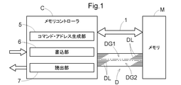
- FIG. 1 shows a memory controller C that reads and writes data from and to the memory M.
- the memory M and the memory controller C are not limited to personal computers, but are intended for audio devices, in-vehicle car navigation devices, portable communication devices, and the like.
- the memory M is assumed to be a DRAM capable of reading and writing data in a burst mode via a 16-bit data bus D (an example of a data transmission lane). That is, for the memory M, a general memory having no special function can be used.
- a command / address line 1 is provided between the memory M and the memory controller C.
- the data bus D has a plurality (16) of signal lines DL arranged in parallel. Note that the data bus D is not limited to 16 bits, and may be 16 bits or more or less.
- the data bus D has a structure in which a first transmission lane DG1 and a second transmission lane DG2 which are 8-bit buses are arranged in parallel, and is configured such that the memory controller C can manage each independently. .
- data is transmitted in synchronization with a reference clock for data transmission.
- a reference clock for data transmission.
- noise having a frequency synchronized with the reference clock is generated.
- FIG. 4A when a bit string in which two “1” s and “0” s are alternately continued is generated, noise having a frequency half that of the reference clock is generated.
- various patterns of bit strings can appear, such as those shown as examples in FIGS. 4B and 4C.
- noise is an electromagnetic wave, there is a possibility of causing problems such as generating unintended signals in peripheral circuits.
- a bit string pattern having a high appearance frequency may generate more noise. Even when the appearance frequency is not high, noise of a specific frequency may easily cause a problem depending on the configuration of peripheral circuits.
- the memory controller C indicates as “replacement bit string” in FIG. It has a function of converting to a bit string having another frequency.
- the “1” and “0” to be replaced are replaced with three “replacement bit strings” that are alternately and continuously arranged. Thereby, noise having the same frequency as that of the reference clock generated in the signal line DL is reduced.
- the replacement bit string written in the memory M is read, the original bit string is restored by the restoration process.
- the bit string in which “1” and “0” in the transmission data received by the memory controller C for writing in the memory M is referred to as an initial bit string.
- an arrangement of “1” and “0” set as replacement targets is referred to as a target pattern.
- a pattern set to be different from the target pattern by replacement is referred to as a post-replacement pattern, and an array of “1” and “0” of this post-replacement pattern is referred to as a replacement bit string.
- a bit string in which “1” and “0” are alternately continued is set as the target pattern, and a bit string in which “1” and “0” are alternately repeated in three is used as the replacement pattern. It is set.
- the data transmitted to the signal line DL It is possible to reduce noise of a specific frequency, that is, noise of a frequency generated by a bit string set in the target pattern. Note that how to set the target pattern will be described later.
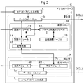
- the memory controller C includes a command / address generation unit 5 that designates a data read / write command and an address, a writing unit 6 that writes transmission data to the memory M, and a memory M And a reading unit 7 for reading data.
- This memory controller C has a function of executing a predetermined process by a program as in the case of a microprocessor, a DSP or the like. By using this function, the memory controller C realizes replacement processing and restoration processing described later. That is, in this embodiment, both the function of the writing unit 6 including the replacement unit that performs the replacement process and the function of the reading unit 7 including the recovery unit that performs the recovery process are realized by a program in the memory controller C. . Therefore, according to the configuration of the present embodiment, a general memory is used as the memory M, and only the functions of the writing unit 6 and the reading unit 7 described below are added to the program of the memory controller C. The structure which can suppress effectively is implement
- the writing unit 6 includes a data write unit 6a and a replacement unit 6b.
- the replacement unit 6b is configured to write before the data is written in the memory M when the arrangement of bit strings “1” and “0” of the transmission data written to the memory M via the signal line DL is the target pattern set as the replacement target.
- processing is performed to replace the initial bit string of the target pattern with a replacement bit string in which the arrangement of “1” and “0” is a post-replacement pattern different from the target pattern.
- the replacement unit 6 b includes a replacement module 11, a pattern determination module 12, an appearance frequency table 13, a storage module 14, and a storage circuit 15.
- the pattern determination module 12 determines whether the sequence of “1” and “0” in the bit string of the transmission data is a target pattern.
- the replacement module 11 replaces the initial bit string of the target pattern with a replacement bit string.
- the storage module 14 stores the target pattern and the address data for specifying the address of the memory M to which the replacement bit string is written in the storage circuit 15 in association with each other.
- the storage circuit 15 is provided inside, but the target for storing data by the storage module 14 may be a partial area of the memory M.
- the reading unit 7 includes a data read unit 7a and a restoration unit 7b.
- the restoration unit 7b performs processing for restoring the replacement bit string of the data read from the memory M to the initial bit string.
- the restoration unit 7 b includes a restoration module 21 and a specific module 22.
- the specifying module 22 specifies a replacement bit string included in the data read from the memory M based on the address data stored in the storage circuit 15.
- the restoration module 21 restores the replacement bit string to the initial bit string before replacement based on the target pattern associated with the address data stored in the storage circuit 15.
- the data write unit 6a writes transmission data to the memory M based on information from the command / address generator 5.
- two command / address generation units 5 are shown for ease of understanding. However, normally, one command / address generation unit 5 may be provided in the memory controller C.
- FIG. This figure shows a data structure in which a plurality of target patterns are stored in the order of appearance frequency, pattern (01), pattern (02)... Pattern (20).
- bit string information is associated with each pattern in order to identify each pattern, and a reference value E is set for distinguishing a plurality of target patterns based on the appearance frequency. Yes.
- This appearance frequency table 13 can be obtained by analysis by a noise analyzer AN described later.
- FIG. 8 is a graph showing an example of the appearance frequency of a bit string pattern that causes noise for each frequency, with the frequency as the horizontal axis and the appearance frequency as the vertical axis.
- the reference value E can be set to, for example, an average value of appearance frequencies for each predetermined frequency range. In place of the average value, the reference value E may be set based on another reference such as the maximum value or the median value.
- the appearance frequency of the bit string pattern that causes noise at each frequency substantially corresponds to the magnitude of noise at each frequency, the vertical axis in the graph of FIG. 8 can be replaced with the noise level.
- the bit length of the bit string of the target pattern is preferably set to be the same as the bit length transferred in the burst mode, but shorter than the bit length transferred in the burst mode. It may be set to a bit string.
- the replacement module 11 acquires initial transmission data to be written to the memory M by the memory controller C, and provides it to the pattern determination module 12.
- the pattern determination module 12 refers to the appearance frequency table 13 to determine whether the arrangement of “1” and “0” of the transmission data of the data transferred to the plurality of data transmission lanes (DG1, DG2) is the target pattern. Determine whether or not.
- a pattern having a lower appearance frequency than the reference value E is set as a post-replacement pattern.
- a processing form is performed so that a bit string that is not stored in the appearance frequency table 13 is a replacement bit string. May be set.
- all patterns having an appearance frequency higher than the reference value E in the appearance frequency table 13 shown in FIG. 7 may be set as the target pattern. In this case, in this determination, whether the bit string information associated with each pattern having an appearance frequency higher than the reference value E in the appearance frequency table 13 matches the target pattern by comparing the initial bit string of the transmission data. A determination is made.
- the replacement module 11 executes replacement processing for replacing the initial bit string of the target pattern with a replacement bit string corresponding to the post-replacement pattern based on the post-replacement pattern set as described above. Then, in association with the replacement, the storage module 14 stores the target pattern in association with the address data for specifying the address of the memory M to which the replacement bit string replaced as matching with the target pattern is written. Store in circuit 15. Then, the replacement bit string after the replacement is written in the memory M. Note that data of an initial bit string having a pattern different from the target pattern is written in the memory M as it is (steps # 103 to # 105).
- the storage module 14 acquires the target pattern related to the initial bit string replaced by the replacement module 11 from the replacement module 11 or the pattern determination module 12, and specifies the address of the memory M in which the replacement bit string is written. Address data is acquired from the data write unit 6a. After this acquisition, these are written in the storage circuit 15 in a state of being associated with each other.
- the address data is generally a combination of the start address of the area in the memory M where the replacement bit string is written and the bit length data.
- a bit string that is the same pattern as the replaced pattern in the state of the initial bit string that has not been subjected to the replacement process by the replacement module 11 is a target bit string for storing an address, and a memory in which the target bit string is written
- the data specifying the address of M is also suitable as the address data.
- the target pattern is often set to a pattern having a high appearance frequency
- the replacement pattern is often set to a pattern having a low appearance frequency.
- the latter is more likely to be smaller in the number of occurrences of bit strings that match the target pattern and the number of occurrences of bit strings that are the same pattern as the replacement pattern in the initial bit string state. Therefore, it is necessary to store the address of the bit string that is the same pattern as the post-replacement pattern in the initial bit string state in the storage circuit 15 as compared with the address information of the address of the bit string that matches the target pattern.
- the number of address information, that is, the data amount can be reduced.
- DG1, DG2 When a plurality of data transmission lanes (DG1, DG2) are provided as in this embodiment, it is preferable to set different post-substitution patterns for each of the plurality of data transmission lanes (DG1, DG2). . In this case, it is preferable to set the post-replacement pattern so that the on / off frequencies of the post-replacement bit string transmitted through each of the plurality of data transmission lanes (DG1, DG2) are different from each other. Thereby, it can suppress that the noise of a specific frequency increases by the replacement process by the replacement unit 6b.
- the replacement unit 6b includes an on / off frequency generated by a sequence of “1” and “0” of the replacement bit string transmitted via the first transmission lane DG1, and the second transmission lane DG2.
- Different permutation patterns are set in the first transmission lane DG1 and the second transmission lane DG2 so that the on / off frequencies generated due to the sequence of “1” and “0” in the permutation bit string to be transmitted are different. For example, if the replacement pattern of the first transmission lane DG1 is the bit string pattern shown in FIG. 4B and the replacement pattern of the second transmission lane DG2 is the bit string pattern shown in FIG.
- the on / off frequency based on the bit string after replacement of the lane DG1 is 1/4 of the reference clock
- the on / off frequency based on the bit string after replacement of the second transmission lane DG2 is 1/8 of the reference clock.
- the target pattern for the first transmission lane DG1 and the target pattern for the second transmission lane DG2 may be the same or different.
- it is preferable that the on / off frequencies of the replacement bit strings transmitted in the respective data transmission lanes are different from each other.
- the replacement bit strings for some data transmission lanes This does not prevent the on / off frequencies of the signals from becoming the same.
- the replacement unit 6b is transmitted via the second transmission lane DG2 and the timing of the boundary between the replacement bit string “1” and “0” transmitted via the first transmission lane DG1.
- Different replacement patterns are set in the first transmission lane DG1 and the second transmission lane DG2 so that the timing of the boundary between “1” and “0” in the replacement bit string differs.
- the replacement pattern of the first transmission lane DG1 is the bit string pattern shown in FIG. 4D and the replacement pattern of the second transmission lane DG2 is the bit string pattern shown in FIG.
- the permutation bit string of the lane DG1 and the permutation bit string of the second transmission lane DG2 have different timings at the boundary between “1” and “0”, and have different on / off frequencies.
- the replacement pattern of the first transmission lane DG1 is the bit string pattern shown in FIG.
- the replacement pattern of the second transmission lane DG2 is the bit string pattern shown in FIG.
- the bit string after replacement of the first transmission lane DG1 and the bit string after replacement of the second transmission lane DG2 have the same on / off frequency, but have different timings at the boundary between “1” and “0”.
- the target pattern for the first transmission lane DG1 and the target pattern for the second transmission lane DG2 may be the same or different.
- it is preferable that the timing of the boundary between “1” and “0” of the replacement bit string transmitted in each is set to be different from each other. This does not prevent the timing of the boundary between “1” and “0” of the replacement bit string for the data transmission lane from being the same.
- the replacement unit 6b performs a replacement process for replacing the initial bit string of the target pattern with the replacement bit string of the replaced pattern for each corresponding data transmission lane (DG1, DG2).
- the data read by the data read unit 7a is given to the restoration module 21.
- the data read unit 7 a gives information on the designated address to the specific module 22, and the specific module 22 compares it with the address specified by the address data stored in the storage circuit 15. In this comparison, it is determined whether the designated address corresponds to an address specified by the address data stored in the storage circuit 15.
- the specification module 22 determines the address specified by the corresponding address data among the data read from the memory M. And the information of the target pattern associated with the address data are given to the restoration module 21. As a result, the restoration module 21 restores the data read from the memory M and transfers the restored data to the request source. If restoration is not necessary, the acquired data is transmitted as it is (steps # 203 to # 206).
- the appearance frequency table 13 determines whether a bit string “1” or “0” of transfer data transferred to the memory M via the signal line DL is included in any of a plurality of preset target patterns; If it is included, it is used to determine which target pattern it is.
- the appearance frequency table 13 has a data structure that stores patterns having a high appearance frequency and patterns having a low appearance frequency.
- This appearance frequency is set based on the appearance frequency information acquired in advance by the noise analyzer AN shown in FIG.
- the memory controller C implements a process according to a program in the same manner as a microprocessor, a DSP, or the like.
- the noise analyzer AN shown in FIG. 10 is configured by setting the program of the memory controller C using this configuration.
- a dedicated computer or the like is connected, and the output appearance frequency information is acquired by the dedicated computer or the like and stored in the appearance frequency table 13.
- the noise analyzer AN itself may be configured to generate the appearance frequency table 13 or update it as needed based on the appearance frequency information.
- the noise analyzer AN includes a data read unit 31, a data write unit 32, a pattern determination unit 33, a determination pattern table 34, an integration processing unit 35, a frequency output unit 37, and a device identification unit. 38 and an output timing setting unit 39.
- the pattern determination unit 33 matches the pattern of arrangement of “1” and “0” of the bit string of the transmission data read / written to / from the memory M via the signal line DL with at least one set determination pattern. It is determined whether or not.
- the determination pattern table 34 stores information on at least one set determination pattern, specifically a bit string of the determination pattern.
- the integration processing unit 35 acquires the number of appearances of the determination pattern determined by the pattern determination unit 33 as an integrated value.
- the frequency output unit 37 outputs the appearance frequency information in which the integrated value acquired by the integration processing unit 35 and the pattern specifying information for specifying the determination pattern represented by the integrated value are associated with each other.
- the noise analyzer AN when various devices actually access the data stored in the memory M, the pattern of “1” and “0” transmitted through the signal line DL is acquired. The frequency of appearance of each pattern is acquired.
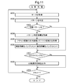
- the flowchart of FIG. 11 shows an outline of the processing. Further, the target of obtaining the appearance frequency information is a bit string of transmission data that matches at least one determination pattern set as an analysis target.
- the pattern determination unit 33 acquires the transmission data. Then, based on the data of the determination pattern table 34, it is determined whether or not it matches at least one set determination pattern (steps # 301 to # 303).
- the integration processing unit 35 acquires the number of appearances of the determination pattern determined by the pattern determination unit 33 as an integrated value.
- the integration processing unit 35 acquires pattern specifying information for specifying the determination pattern for transmission data determined to match the determination pattern by the pattern determination unit 33, and integrates the number of appearances for each determination pattern.
- the integration processing unit 35 acquires the integration value by distinguishing between the case where data is written to the memory M and the case where data is read from the memory M.
- the integration processing unit 35 calculates an integrated value for each segment area according to which of the plurality of segment areas in the storage area of the memory M the address in the memory M to which transmission data is written belongs. get.
- the integration processing unit 35 acquires an integration value for each device, depending on which of the plurality of devices that can access the memory M is the transmission data transmission source device. For this purpose, the integration processing unit 35 acquires attribute information including access information, segmented region information, and device information for transmission data determined as a determination pattern by the pattern determination unit 33. Then, the attribute information is associated with the acquired pattern specifying information, the number of appearances of each determination pattern is integrated, and acquired as an integrated value (steps # 304 to # 306).
- FIG. 9 shows an example of integrated value data associated with the pattern specifying information and attribute information acquired by the integration processing unit 35.
- each piece of integrated value data uses pattern specifying information as an index, and attribute information includes access information indicated by (R) and (W), (A1 To A3) and segment information (D1 to D3).
- the pattern specifying information is associated with bit string information of a determination pattern specified by the pattern specifying information.
- the access information (R) and (W) is distinguished between when data (bit string information) is written to the memory M (R) and when data (bit string information) is read from the memory M (W).
- the divided area information (A1 to A3) is an address in the memory M to which the transmission data (bit string information) of the determination pattern is written, which of the divided areas (A1 to A3) in the storage area of the memory M. It belongs to.
- Device information (D1 to D3) indicates which of the plurality of devices (D1 to D3) that can access the memory M is the transmission source device of the transmission data (bit string information) of the determination pattern. Yes.
- which device is the transmission source is identified by the device identification unit 38, and the identification information is given to the integration processing unit 36.
- the segment area information is not limited to the above three areas, and the number of devices is not limited to three.
- the integration processing unit 35 integrates the number of appearances for each determination pattern specified by the pattern specifying information and for each attribute information, and increments the integrated value (step # 306). Specifically, every time the bit string of the transmission data read / written to / from the memory M matches the determination pattern, the integration processing unit 35 uses the pattern specifying information about the transmission data (bit string information) and ( Access information indicated by (R) and (W), segmented area information indicated by (A1 to A3), and device information indicated by (D1 to D3) are acquired. Then, according to the acquired information, the integration processing unit 35 uses the access information (R) for the integrated value data as shown in FIG. 9 and the pattern identification information for specifying the determination pattern. And any value of (W) is incremented, any value of (A1 to A3) of the segment area information is incremented, and any of (D1 to D3) of the device information is incremented.
- the frequency output unit 37 outputs appearance frequency information at a preset output timing (steps # 307 and # 308).
- the appearance frequency information is information in which the integrated value acquired by the integration processing unit 35 is associated with pattern specifying information for specifying the determination pattern represented by the integrated value.
- the appearance frequency information is also attribute information including access information, segmented area information, and device information that is associated with the integrated value and the pattern specifying information.
- the frequency output unit 37 acquires the integrated value data (see FIG. 9) at the time when the output timing comes from the integration processing unit 35, and outputs the integrated value data at that time as appearance frequency information. To do. Further, the processes in steps # 301 to # 308 are repeatedly executed until reset (step # 309).
- the output timing setting unit 39 gives output trigger information to the frequency output unit 37 in accordance with the set output timing.
- the frequency output unit 37 outputs appearance frequency information according to the trigger information.
- the output timing setting unit 39 is a frequency output unit every time the integrated value by the integration processing unit 35 exceeds a preset output threshold value or every time the integration period of the integrated value exceeds a preset output period.
- 37 gives output trigger information.
- the output timing setting unit 39 integrates the integrated value data every time the integrated value of each item of the integrated value data shown in FIG. 9 exceeds the preset output threshold.
- trigger information is output to the frequency output unit 37.
- the output timing setting unit 39 is triggered whenever both a value condition that the preset output threshold is exceeded and a period condition that the integration period of the integration value of the integration value data exceeds the preset output period are satisfied. It may be configured to output information.
- the appearance frequency information obtained by this analysis process Based on the appearance frequency information obtained by this analysis process, by sorting the integrated values of each attribute information, the appearance frequency based on any one of the access information and the segmented area information device information or a combination thereof can be obtained. Obtainable.
- the storage area of the memory M is divided into a plurality of divided areas in advance, and different types of data are stored for each divided area.
- map information is stored in the first partitioned area
- still image information is stored in the second partitioned area
- audio information is stored in the third partitioned area
- a program is stored in the fourth partitioned area.
- the division area stored for each data type is determined in advance.
- different types of data may be transmitted for each device.
- the map drawing device transmits map data
- the image display device transmits still image data
- the audio playback device transmits audio information.
- different types of data transmission may be performed for each device that accesses the memory M, such as an arithmetic processing device transmitting program data.
- the frequency of appearance of the combination pattern of “1” and “0” of the bit string of data transmitted between the memory controller C and the memory M is also biased. A certain tendency may appear in Therefore, the pattern having a high appearance frequency in the bit string of the transmission data may be different for each divided area in the memory M or for each device accessing the memory M.
- the target pattern and the post-replacement pattern is made different depending on which of the devices. For example, on the basis of the above-described appearance frequency information, the appearance frequency for each partition area of the memory M is acquired, and at least one of the patterns whose appearance frequency is higher than the reference value E for each partition area to which the address to which the transmission data is written belongs. One may be set as the target pattern, and at least one of the patterns having an appearance frequency lower than the reference value E may be set as the replacement pattern.
- the appearance frequency of each transmission data transmission source device is obtained, and at least one of the patterns having the appearance frequency higher than the reference value E is obtained for each transmission data transmission source device. It may be set as a target pattern, and at least one of patterns whose appearance frequency is lower than the reference value E may be set as a replacement pattern.
- each of the data transmission lanes (DG1, DG2) includes a plurality of signal lines DL has been described as an example.
- each of the data transmission lanes (DG1, DG2) may be configured by one signal line DL.
- the target pattern and the post-replacement pattern may be set for each signal line DL.
- the post-replacement pattern is set from patterns whose appearance frequency is lower than the reference value E has been described as an example.
- the post-replacement pattern may be a bit string in which only “0” is continuous or a bit string in which only “1” is continuous.
- all the replacement bit strings have the same potential in the signal line DL, so that noise can be effectively reduced.
- the target pattern is set to at least one of patterns whose appearance frequency is higher than the reference value E
- the replacement pattern is set to at least one of the patterns whose appearance frequency is lower than the reference value E.
- the target pattern and the post-replacement pattern may be set based on a criterion other than the appearance frequency. For example, at least one of the patterns in which the sequence of bit strings “1” and “0” included in the data before replacement by the replacement unit 6b generates noise in a predetermined noise frequency range is targeted. It is also preferable that the pattern is set and at least one of the patterns other than the pattern that generates noise in the noise frequency range is set as the replacement pattern.
- the appearance frequency information output by the frequency output unit 37 is information in which the integrated value, the pattern specifying information, and the attribute information are associated with each other.
- the appearance frequency information may be information obtained by associating the integrated value with the pattern specifying information.
- the attribute information may be configured to include only a part of these, or may be configured to include information other than these.
- the memory controller (C) designates the address of the memory (M) and designates the address of the memory (M) and the writing unit (6) for writing data to the memory (M) via the signal line (DL).
- a reading section (7) for reading data from the memory (M) via the signal line (DL);
- the replacement before writing to the memory (M), the replacement is performed by replacing the initial bit string of the target pattern with a replacement bit string in which the arrangement of “1” and “0” is different from the target pattern.
- a unit (6b) The reading unit (7) includes a restoration unit (7b) that restores the replacement bit string of the data read from the memory (M) to the initial bit string.
- noise generated in the signal line (DL) can be reduced.
- noises of various frequencies can be reduced only by changing the setting of the target pattern and the replacement pattern in software. Therefore, for example, a noise frequency to be reduced can be easily changed as compared with a case where a shield is provided to cover the signal line (DL) or noise countermeasures are taken by circuit design. Therefore, noise countermeasures can be flexibly implemented according to the usage environment of the memory (M) and the memory controller (C).
- the replacement unit (6b) A pattern determination module (12) for determining whether the sequence of “1” and “0” of the bit string of the transmission data is the target pattern; A replacement module (11) that replaces the initial bit string with the replacement bit string when the pattern determination module (12) determines that the pattern is the target pattern; When the replacement by the replacement module (11) is performed, a storage module (in which the target pattern and address data for specifying the address of the memory (M) to which the replacement bit string is written are stored in association with each other.
- the restoration unit (7b) A specifying module (22) for specifying the replacement bit string included in the data read from the memory (M) based on the address data; A restoration module (21) that restores the replacement bit string to the initial bit string before replacement based on the target pattern associated with the address data is preferably provided.
- the replacement module (11) replaces the initial bit string of the target pattern with the replacement bit string.
- the replacement bit string rewritten in this way is written into the memory (M).
- the target pattern and the address data are associated with each other and stored in a predetermined storage unit or the like by the storage module (14).
- the specific module (22) determines that the replacement bit string is included in the data read from the memory (M)
- the replacement bit string is restored to the initial bit string by the restoration module (21).
- the appearance frequency of the pattern of “1” and “0” in the bit string included in the data before replacement by the replacement unit (6b) is higher than a predetermined reference value (E). At least one is set as the target pattern, It is preferable that at least one of the patterns whose appearance frequency is lower than the reference value (E) is set as the replacement pattern.
- the signal line (DL) can be transmitted by replacing the bit string pattern whose appearance frequency is higher than the reference value (E) with the bit string whose pattern appearance frequency is lower than the reference value (E). Accordingly, it is possible to reduce the number of bit string patterns that are highly likely to generate noise due to high appearance frequency, and to reduce noise generated in the signal line (DL).
- At least one of the patterns in which the arrangement of bit strings “1” and “0” included in the data before replacement by the replacement unit (6b) generates noise in a predetermined noise frequency range. is set to the target pattern, It is preferable that at least one of the patterns other than the pattern that generates noise in the noise frequency range is set as the replacement pattern.
- a signal line (DL) can be transmitted by replacing a bit string pattern that generates noise in a predetermined noise frequency range with a bit string having a pattern that does not generate noise in the frequency range. Therefore, it is possible to reduce the number of bit string patterns that generate noise in a specific frequency region that is desired to be reduced, and it is possible to reduce noise in the specific frequency region that is generated in the signal line (DL). When the frequency range where noise is desired to be reduced has already been determined, it is possible to effectively reduce noise by using such a setting.
- a plurality of signal lines (DL), and a plurality of signal lines (DL) constitute a plurality of data transmission lanes including at least a first transmission lane (DG1) and a second transmission lane (DG2);
- the replacement unit (6b) includes an on / off frequency generated by a sequence of “1” and “0” of the replacement bit string transmitted via the first transmission lane (DG1), and via the second transmission lane.
- the first transmission lane (DG1) and the second transmission lane (DG2) are different so that the on / off frequency generated by the “1” and “0” of the replacement bit string to be transmitted is different. It is preferable to set a pattern.
- a plurality of signal lines (DL), and a plurality of signal lines (DL) constitute a plurality of data transmission lanes including at least a first transmission lane (DG1) and a second transmission lane (DG2);
- the replacement unit (6b) includes a timing of a boundary between “1” and “0” of the replacement bit string transmitted via the first transmission lane (DG1), and the second transmission lane (DG2).
- the post-replacement patterns that are different in the first transmission lane (DG1) and the second transmission lane (DG2) so that the timing of the boundary between “1” and “0” of the permutation bit string transmitted in different ways Is preferably set.
- the timing of the boundary between “1” and “0” of the bit string after replacement in the plurality of data transmission lanes (DG1, DG2) is the same. It is possible to suppress an increase in noise at the timing due to the above.
- the writing unit (6) determines whether the address to which the transmission data is written belongs to which of a plurality of divided areas in the storage area of the memory (M) or the transmission data It is preferable that at least one of the target pattern and the replacement pattern is made different depending on which of the plurality of devices that can access the memory (M) is a transmission source device.
- the storage area of the memory (M) may be divided into a plurality of divided areas in advance, and different types of data may be stored for each divided area. Further, there are cases where there are a plurality of devices accessible to the memory (M), and different types of data may be transmitted for each device. And according to such data type, there is also a bias in the appearance frequency of the combination pattern of “1” and “0” of the bit string of data transmitted between the memory controller (C) and the memory (M). May occur, and a certain tendency may appear in the bias. Therefore, the pattern having a high appearance frequency in the bit string of the transmission data may be different for each divided area in the memory (M) or for each device accessing the memory (M). According to the above configuration, it is possible to appropriately set at least one of the target pattern and the post-replacement pattern according to such a bias for each data type. Accordingly, noise generated in the signal line (DL) can be effectively reduced.
- the post-replacement pattern is a bit string in which only “0” is continuous or a bit string in which only “1” is continuous.
- the replacement bit strings all have the same potential in the signal line (DL), noise can be effectively reduced. Also, when such a post-replacement pattern is used, it is possible to replace all of the initial bit strings of a plurality of patterns that are likely to generate noise with a replacement bit string in which only “0” or “1” is continuous. Accordingly, it is possible to improve the processing speed by simplifying the processing in the replacement unit (6b).
- the technology according to the present disclosure can be used for a memory controller that transmits data to a memory via a signal line.
Landscapes
- Engineering & Computer Science (AREA)
- Theoretical Computer Science (AREA)
- Physics & Mathematics (AREA)
- General Engineering & Computer Science (AREA)
- General Physics & Mathematics (AREA)
- Human Computer Interaction (AREA)
- Quality & Reliability (AREA)
- Spectroscopy & Molecular Physics (AREA)
- Computer Networks & Wireless Communication (AREA)
- Signal Processing (AREA)
- Computer Security & Cryptography (AREA)
- Dc Digital Transmission (AREA)
- Techniques For Improving Reliability Of Storages (AREA)
- Communication Control (AREA)
- Memory System (AREA)
Abstract
メモリにデータを転送する際に発生するノイズを抑制する。 メモリコントローラ(C)が、メモリに伝送データを書き込む書込部(6)と、メモリからデータを読み出す読出部(7)とを備えている。書込部(6)が、信号ライン(DL)に伝送されるデータを構成するビット列の「1」と「0」との並びパターンが、置換対象として設定された対象パターンである場合に、メモリに書き込む以前に、そのビット列をノイズが抑制される置換ビット列に置き換える置換ユニット(6b)を備えている。読出部(7)が、メモリから読み出した置換ビット列を初期ビット列に復元する復元ユニット(7b)を備えている。
Description
本発明は、メモリに対して信号ラインを介してデータ伝送を行うメモリコントローラに関する。
上記の技術として、例えば、下記の特許文献1には、信号ライン(引例ではデータバス)の各ビットを、符号化回路により2ビット以上の転送データに変換してデータバスに送り出し、データバスを送られた転送データを、復号回路により元のデータに復元することでバスノイズを低減するものが開示されている。
この特許文献1の技術では、転送データの複数のビットが同時に「1」又は「0」の状態から「0」又は「1」の状態へ変化するというような極端な変化が回避されることにより、電源や接地電位に対するノイズの発生を防止している。
しかし、メモリコントローラとメモリとの間のデータバスを考えると、データバスに送られるデータは「1」と「0」との組み合わせで成るため、例えば、「1」と「0」とが交互に伝送される場合等のように信号変化が一定周期で繰り返し発生することに起因する、特定周波数のノイズの発生を抑制することは困難であった。
また、特許文献1の技術では、メモリコントローラからメモリに対しての書込みと読出しの双方に対応するためには、転送データを生成するための符号化回路と、転送データを元のデータに復元するための復号回路とが、メモリコントローラとメモリの双方に必要となる。更に、特許文献1の技術では、信号変化の2倍以上の周波数のクロック信号が必要であるため、メモリコントローラとメモリの双方に専用のクロック生成回路を備える必要がある。また符号化回路と復号回路とをメモリコントローラとメモリの双方に備えるため、符号化と復号の双方についてのソフトウエア設定も、メモリコントローラとメモリの双方に必要となり、これらのソフトウエア設定の手順が多くならざるを得ない。以上のことから、特許文献1の技術では、メモリコントローラとメモリの双方のコストが上昇するだけでなく、これらの双方に符号化回路と復号回路とを配置するための回路基板のスペースの確保を必要とする課題がある。
また、ノイズの影響を抑制するために、金属性のシールドを回路基板に設けたり、回路設計を変更したりすることなども行われているが、このような対策はコストの上昇の要因になると共に、変更が容易ではないために、様々な使用環境やノイズ要因に応じて柔軟に対策をとることが困難であるという問題があった。
そこで、メモリに対して信号ラインを介してデータ伝送を行う構成において、信号ラインで発生するノイズを効果的に抑制することができる技術が求められる。
上記に鑑みたメモリコントローラの技術的特徴は、メモリのアドレスを指定し信号ラインを介してメモリにデータを書き込む書込部と、前記メモリのアドレスを指定し前記信号ラインを介して前記メモリからデータを読み出す読出部とを備え、
前記書込部が、前記信号ラインを介して前記メモリに書き込まれる伝送データのビット列の「1」と「0」との並びが置換対象として設定された対象パターンである場合に、前記メモリに書き込む以前に、前記対象パターンの初期ビット列を、「1」と「0」との並びが前記対象パターンとは異なる置換後パターンとなる置換ビット列に置き換える置換ユニットを備え、
前記読出部が、前記メモリから読み出したデータの前記置換ビット列を前記初期ビット列に復元する復元ユニットを備えている点にある。
前記書込部が、前記信号ラインを介して前記メモリに書き込まれる伝送データのビット列の「1」と「0」との並びが置換対象として設定された対象パターンである場合に、前記メモリに書き込む以前に、前記対象パターンの初期ビット列を、「1」と「0」との並びが前記対象パターンとは異なる置換後パターンとなる置換ビット列に置き換える置換ユニットを備え、
前記読出部が、前記メモリから読み出したデータの前記置換ビット列を前記初期ビット列に復元する復元ユニットを備えている点にある。
この構成によれば、対象パターン及び置換後パターンを適切に設定することにより、問題となるノイズを発生させるビット列のパターンを別のパターンに置き換えることができるため、メモリに対してデータを書き込む場合とメモリからデータを読み出す場合の双方において、信号ラインで発生するノイズを低減することが可能となる。
またこの際、ソフトウエア的に対象パターン及び置換後パターンの設定を変更するだけで様々な周波数のノイズを低減することができる。従って、例えば信号ラインを覆うシールドを設け、或いは、回路設計によりノイズ対策を行う場合に比べ、容易に低減対象のノイズ周波数を変更することができる。従って、メモリ及びメモリコントローラの使用環境に応じて柔軟にノイズ対策を実施できる。
更に、この構成によれば、置換ユニットの機能と復元ユニットの機能とをメモリコントローラに装備させるだけでよく、メモリについては一般的なものを使用することが可能である。ソフトウエア設定についても、メモリコントローラのみの設定で済むため、ソフトウエア設定手順を簡略化することが可能である。
以下、本発明の実施形態を図面に基づいて説明する。
1.実施形態
〔基本構成〕
メモリコントローラCの実施形態について図面に基づいて説明する。図1にはメモリMに対してデータの読み書きを行うメモリコントローラCを示している。このメモリMとメモリコントローラCとは、パーソナルコンピュータに限らず、オーディオ機器や、車載のカーナビゲーション機器、携帯通信機器等に備えられるものを対象としている。
1.実施形態
〔基本構成〕
メモリコントローラCの実施形態について図面に基づいて説明する。図1にはメモリMに対してデータの読み書きを行うメモリコントローラCを示している。このメモリMとメモリコントローラCとは、パーソナルコンピュータに限らず、オーディオ機器や、車載のカーナビゲーション機器、携帯通信機器等に備えられるものを対象としている。
メモリMは、16ビットのデータバスD(データ伝送レーンの一例)を介し、バーストモードでのデータの読み書きが可能なDRAMを想定している。すなわち、メモリMについては特別な機能を有しない一般的なメモリを用いることができる。メモリMとメモリコントローラCとの間には、コマンド・アドレスライン1を備えている。データバスDは複数(16本)の信号ラインDLを並列に配置したものである。尚、データバスDは16ビットに限らず、16ビット以上や、これ未満のビット数でも良い。
また、データバスDは、8ビットのバスとなる第1伝送レーンDG1と第2伝送レーンDG2とを並列した構造を有し、メモリコントローラCが各々を独立して管理できるように構成されている。
データバスD(データ伝送レーン)を構成する複数の信号ラインDLでは、データ伝送の基準クロックに同期してデータを伝送するめ、例えば、図3に「初期ビット列」として示すように、データが「1」と「0」とが交互に連続するビット列となる場合には、基準クロックに同期した周波数のノイズが発生する。また、例えば図4(a)に示すように、「1」と「0」とが2個ずつ交互に連続するビット列となる場合には、基準クロックの半分の周波数のノイズが発生する。尚、伝送されるビット列の具体例は、これらの他にも、例えば図4において(b)、(c)として例を挙げたもののように、様々なパターンのビット列が出現し得る。ノイズは電磁波であるため、周辺の回路に意図しない信号を発生させるなどの問題を生じさせる可能性もある。前記のようなビット列のパターンに応じて生じる各周波数のノイズのうちで、出現頻度が高いビット列のパターンが、より多くのノイズを発生させる可能性がある。また、出現頻度が高くない場合であっても、周辺の回路の構成等によって特定の周波数のノイズが特に問題を生じさせ易い場合もあり得る。
このような理由から、メモリコントローラCは、例えば図3に示すように、「初期ビット列」が特定の周波数のノイズを発生させるビット列である場合には、同図に「置換ビット列」として示すように他の周波数となるビット列に変換する機能を有している。尚、図3に示す例では、基準クロックと同じ周波数のノイズを発生させる「1」と「0」とが交互に連続する「初期ビット列」を、基準クロックの1/3の周波数のノイズを発生させる「1」と「0」とが3個ずつ交互に連続する「置換ビット列」に置換している。これにより、信号ラインDLで発生する基準クロックと同じ周波数のノイズを低減している。更に、このメモリコントローラCでは、メモリMに書き込まれた置換ビット列を読み出した場合には、復元処理により元のビット列に復元される。
この実施形態では、メモリMに書き込むためメモリコントローラCが受け取った伝送データの「1」と「0」との並びのビット列を初期ビット列と称している。また、初期ビット列のうち、置換対象に設定された「1」と「0」との並びを対象パターンと称している。更に、置換により対象パターンと異なるように設定されたパターンを置換後パターンと称し、この置換後パターンの「1」と「0」との並びを置換ビット列と称している。図3に示す例では、「1」と「0」とが交互に連続するビット列を対象パターンに設定し、「1」と「0」とが3個ずつ交互に連続するビット列を置換後パターンに設定している。
これにより、メモリMにデータが伝送される場合(書き込まれる場合)と、メモリMからデータが伝送される場合(読み出される場合)との何れの場合にも、信号ラインDLに伝送されるデータにおける特定の周波数のノイズ、すなわち対象パターンに設定されたビット列により生じる周波数のノイズの低減を行うことができる。なお、対象パターンをどのように設定するかについては、後述する。
〔メモリコントローラ〕
図1に示すように、メモリコントローラCは、データの読み書きのコマンドとアドレスを指定するコマンド・アドレス生成部5と、メモリMへの伝送データの書き込みを実行する書込部6と、メモリMからデータの読み出しを実行する読出部7とを備えている。
図1に示すように、メモリコントローラCは、データの読み書きのコマンドとアドレスを指定するコマンド・アドレス生成部5と、メモリMへの伝送データの書き込みを実行する書込部6と、メモリMからデータの読み出しを実行する読出部7とを備えている。
このメモリコントローラCは、マイクロプロセッサやDSP等と同様にプログラムにより所定の処理を実行する機能を有するものである。この機能を利用することにより、メモリコントローラCは、後述する置換処理と復元処理とを実現する。すなわち、本実施形態では、置換処理を行う置換ユニットを含む書込部6の機能と、復元処理を行う復元ユニットを含む読出部7の機能とは、いずれもメモリコントローラCにおけるプログラムにより実現される。従って、本実施形態の構成によれば、メモリMとしては一般的なものを用い、メモリコントローラCのプログラムに、以下で説明する書込部6と読出部7の機能を追加するだけで、ノイズを効果的に抑制することができる構成が実現される。
図2に示すように、書込部6は、データライトユニット6aと、置換ユニット6bとを備えている。置換ユニット6bは、信号ラインDLを介してメモリMに書き込まれる伝送データのビット列の「1」と「0」との並びが置換対象として設定された対象パターンである場合に、メモリMに書き込む以前に、対象パターンの初期ビット列を、「1」と「0」との並びが対象パターンとは異なる置換後パターンとなる置換ビット列に置き換える処理を行う。そのために、置換ユニット6bは、置換モジュール11と、パターン判定モジュール12と、出現頻度テーブル13と、記憶モジュール14と、記憶回路15とを備えている。パターン判定モジュール12は、伝送データのビット列の「1」と「0」との並びが設定された対象パターンであるかを判定する。置換モジュール11は、パターン判定モジュール12で対象パターンであることを判定した場合に、当該対象パターンの初期ビット列を置換ビット列に置き換える。記憶モジュール14は、置換モジュール11での置き換えを行った場合に、対象パターンと、置換ビット列が書き込まれるメモリMのアドレスを特定するためのアドレスデータと、を関連付けて記憶回路15に記憶させる。本実施形態のメモリコントローラCでは、内部に記憶回路15を備えているが、記憶モジュール14によりデータを記憶する対象がメモリMの一部の領域であっても良い。
読出部7は、データリードユニット7aと、復元ユニット7bとを備えている。復元ユニット7bは、メモリMから読み出したデータの置換ビット列を初期ビット列に復元する処理を行う。そのために、復元ユニット7bは、復元モジュール21と特定モジュール22とで構成されている。特定モジュール22は、記憶回路15に記憶されたアドレスデータに基づいて、メモリMから読み出したデータの中に含まれる置換ビット列を特定する。
復元モジュール21は、記憶回路15に記憶されたアドレスデータに関連付けられている対象パターンに基づいて、置換ビット列を置き換え前の初期ビット列に復元する。
復元モジュール21は、記憶回路15に記憶されたアドレスデータに関連付けられている対象パターンに基づいて、置換ビット列を置き換え前の初期ビット列に復元する。
データライトユニット6aは、コマンド・アドレス生成部5からの情報に基づいて伝送データのメモリMへの書き込みを実行する。尚、同図では、理解を容易にするため2つのコマンド・アドレス生成部5を示しているが、通常、このコマンド・アドレス生成部5は、メモリコントローラCに1つ備えられていればよい。
出現頻度テーブル13のデータ構造の一例を図7に示している。同図では、出現頻度が高いものからパターン(01)、パターン(02)‥‥パターン(20)となる順序で複数の対象パターンを記憶したデータ構造であることを示している。また、この出現頻度テーブル13では、各々のパターンを識別するため、各々のパターンにビット列情報が関連付けられており、複数の対象パターンを出現頻度に基づいて区別するための基準値Eが設定されている。この出現頻度テーブル13は、後述するノイズ分析装置ANによる分析により得られたものとすることができる。
図8は、周波数を横軸とし、出現頻度を縦軸として、周波数毎のノイズを生じさせるビット列パターンの出現頻度の一例を表したグラフである。この例では、基準クロックと同じ周波数(周波数=n)のノイズを生じさせるビット列パターンの出現頻度が最も高く、基準値Eを超えている。そこで、本実施形態においては、基準クロックと同じ周波数(周波数=n)のノイズを生じさせる単数又は複数のビット列パターンの少なくとも一つを対象パターンに設定している。また、図8の例では、基準クロックの1/4の周波数(周波数=n/4)のノイズを生じさせるビット列パターンの一つを置換後パターンに設定している。これにより、基準クロックの1/4の周波数(周波数=n/4)のノイズを増加させる代わりに、出現頻度が基準値Eを超えている基準クロック周波数(周波数=n)のノイズを低減することができており、結果的に、全ての周波数において出現頻度が基準値E以下に抑えられている。ここで、基準値Eは、例えば、予め定められた周波数域毎の出現頻度の平均値に設定することができる。なお、平均値に代えて、最多値、中央値等、他の基準に基づいて基準値Eを設定してもよい。また、各周波数のノイズを生じさせるビット列パターンの出現頻度は、実質的に各周波数のノイズの大きさに対応しているため、図8のグラフにおいて、縦軸をノイズレベルと置き換えることもできる。
〔処理形態〕
図5のフローチャートには、書込部6での書き込み処理の概要を示しており、図6のフローチャートには、読出部7での読み出し処理の概要を示している。
図5のフローチャートには、書込部6での書き込み処理の概要を示しており、図6のフローチャートには、読出部7での読み出し処理の概要を示している。
書き込みを実行する場合には、メモリMにバーストモードで書き込むためにメモリコントローラCに与えられた全てのデータについて、対象パターンのビット列であるかの判定が行われる。この判定は、データバスDを構成する複数のデータ伝送レーン(DG1、DG2)の各々について行われ、判定の結果、対象パターンの初期ビット列(対象ビット列)を、置換後パターンのビット列である置換ビット列に置き換える処理が行われる。
なお、バーストモードで書き込みが行われる場合には、対象パターンのビット列のビット長は、バーストモードで転送されるビット長と同じに設定すると好適であるが、バーストモードで転送されるビット長より短いビット列に設定してもよい。
〔処理形態:書き込み処理〕
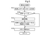
メモリコントローラCに伝送データを伝送してメモリMへの書き込み要求があった場合には、図5のフローチャートに示す書き込み処理が実行される。この書き込み処理では、複数のデータ伝送レーン(DG1、DG2)での伝送データのビット列(初期ビット列)が取得され、各々のパターンの判定が行われる。この判定の結果、予め設定されている対象パターンである場合には置き換え対象に設定する(#101、#102ステップ)。
メモリコントローラCに伝送データを伝送してメモリMへの書き込み要求があった場合には、図5のフローチャートに示す書き込み処理が実行される。この書き込み処理では、複数のデータ伝送レーン(DG1、DG2)での伝送データのビット列(初期ビット列)が取得され、各々のパターンの判定が行われる。この判定の結果、予め設定されている対象パターンである場合には置き換え対象に設定する(#101、#102ステップ)。
この処理では、置換モジュール11が、メモリコントローラCがメモリMに書き込むべき初期の伝送データを取得し、パターン判定モジュール12に与える。パターン判定モジュール12は出現頻度テーブル13を参照することにより、複数のデータ伝送レーン(DG1、DG2)に転送されるデータの伝送データの「1」と「0」との並びが対象パターンであるか否かの判定を行う。
つまり、この判定では、伝送データの初期ビット列が、図7に示す複数のパターンのうち基準値Eより出現頻度が高いものの中から設定された対象パターンと合致した場合に、その初期ビット列を対象パターンのビット列であると判定する。そして、基準値Eより出現頻度が低いパターンの中から設定された置換後パターンのビット列に置き換える。すなわち、本実施形態では、出現頻度が基準値Eより高いパターンの中の少なくとも1つを対象パターンに設定し、出現頻度が基準値Eより低いパターンの中の少なくとも1つを置換後パターンに設定している。以下では、説明の簡略化のため、データ伝送レーン(DG1、DG2)毎に1つの対象パターンと1つの置換後パターンを設定する場合を例として説明する。この処理では、基準値Eより出現頻度が低いパターンを置換後パターンに設定するものであるが、これに代えて、出現頻度テーブル13には記憶されていないビット列を置換ビット列とするように処理形態を設定しても良い。また、例えば、図7に示す出現頻度テーブル13において基準値Eより出現頻度が高いパターンの全てを対象パターンに設定してもよい。その場合には、この判定では出現頻度テーブル13において基準値Eより出現頻度が高い各パターンに関連付けられたビット列情報と、伝送データの初期ビット列との比較により対象パターンに合致するものか否かの判定が行われる。
置換モジュール11は、上記のように設定された置換後パターンに基づいて、対象パターンの初期ビット列を、置換後パターンに対応する置換ビット列に置き換える置換処理を実行する。そして、置き換えに連係して、記憶モジュール14が、対象パターンと、当該対象パターンに合致するとして置き換えられた置換ビット列が書き込まれるメモリMのアドレスを特定するためのアドレスデータとを関連付けた状態で記憶回路15に記憶する。
そして、置換された後の置換ビット列がメモリMに書き込まれる。なお、対象パターンとは異なるパターンの初期ビット列のデータは、そのままメモリMに書き込まれる(#103~#105ステップ)。
そして、置換された後の置換ビット列がメモリMに書き込まれる。なお、対象パターンとは異なるパターンの初期ビット列のデータは、そのままメモリMに書き込まれる(#103~#105ステップ)。
本例では、この処理において、記憶モジュール14が、置換モジュール11により置換した初期ビット列に係る対象パターンを置換モジュール11又はパターン判定モジュール12から取得し、置換ビット列が書き込まれるメモリMのアドレスを特定するためのアドレスデータをデータライトユニット6aから取得する。この取得の後に、これらを互いに関連付けた状態で記憶回路15に書き込む。
アドレスデータは、置換ビット列が書き込まれるメモリM内の領域の先頭アドレスと、ビット長のデータとの組み合わせとするのが一般的である。一方、別の例として、置換モジュール11による置換処理を行っていない初期ビット列の状態で置換後パターンと同じパターンであるビット列を、アドレスを記憶する対象のビット列とし、当該対象のビット列が書き込まれるメモリMのアドレスを特定するデータをアドレスデータとしても好適である。上記のとおり、対象パターンは、出現頻度が高いパターンに設定され、置換後パターンは出現頻度が低いパターンに設定されることが多い。そのような場合、対象パターンに合致するビット列の出現数と、初期ビット列の状態で置換後パターンと同じパターンであるビット列の出現数とでは、後者の方が少なくなる可能性が高い。従って、初期ビット列の状態で置換後パターンと同じパターンであるビット列のアドレスをアドレス情報とする方が、対象パターンに合致するビット列のアドレスをアドレス情報とする場合よりも、記憶回路15に記憶する必要があるアドレス情報の数、すなわちデータ量を低減することができる。
本実施形態のように、複数のデータ伝送レーン(DG1、DG2)を備える場合には、当該の複数のデータ伝送レーン(DG1、DG2)のそれぞれについて、互いに異なる置換後パターンを設定すると好適である。この場合において、複数のデータ伝送レーン(DG1、DG2)のそれぞれを伝送される置換後ビット列によるオンオフ周波数が、互いに異なるオンオフ周波数となるように、置換後パターンを設定すると好適である。これにより、置換ユニット6bによる置換処理によって、特定の周波数のノイズが増加することを抑制できる。そこで、本実施形態では、置換ユニット6bは、第1伝送レーンDG1を介して伝送される置換ビット列の「1」と「0」との並びにより生じるオンオフ周波数と、第2伝送レーンDG2を介して伝送される置換ビット列の「1」と「0」との並びにより生じるオンオフ周波数とが異なるように、第1伝送レーンDG1と第2伝送レーンDG2とで異なる置換後パターンを設定している。例えば、第1伝送レーンDG1の置換後パターンを図4(b)に示すビット列のパターンとし、第2伝送レーンDG2の置換後パターンを図4(c)に示すビット列のパターンとすると、第1伝送レーンDG1の置換後ビット列によるオンオフ周波数が基準クロックの1/4の周波数となり、第2伝送レーンDG2の置換後ビット列によるオンオフ周波数が基準クロックの1/8の周波数となる。この場合において、第1伝送レーンDG1についての対象パターンと、第2伝送レーンDG2についての対象パターンとが、同じであっても良いし、異なっていても良い。なお、データ伝送レーンが3つ以上ある場合、それぞれにおいて伝送される置換ビット列のオンオフ周波数が、互いに異なる周波数となるように設定されると好適であるが、一部のデータ伝送レーンについての置換ビット列のオンオフ周波数が同じになることを妨げるものではない。
また、複数のデータ伝送レーン(DG1、DG2)のそれぞれを伝送される置換後ビット列の「1」と「0」との境界のタイミングが互いに異なるように、置換後パターンを設定すると好適である。これにより、置換ユニット6bによる置換処理の後、複数のデータ伝送レーン(DG1、DG2)での置換後ビット列の「1」と「0」との境界のタイミングが同じになることに起因して当該タイミングでノイズが増加することを抑制できる。そこで、本実施形態では、置換ユニット6bは、第1伝送レーンDG1を介して伝送される置換ビット列の「1」と「0」との境界のタイミングと、第2伝送レーンDG2を介して伝送される置換ビット列の「1」と「0」との境界のタイミングとが異なるように、第1伝送レーンDG1と第2伝送レーンDG2とで異なる置換後パターンを設定している。例えば、第1伝送レーンDG1の置換後パターンを図4(d)に示すビット列のパターンとし、第2伝送レーンDG2の置換後パターンを図4(e)に示すビット列のパターンとすると、第1伝送レーンDG1の置換後ビット列と第2伝送レーンDG2の置換後ビット列とは、「1」と「0」との境界のタイミングが互いに異なると共に、オンオフ周波数も互いに異なるものとなる。また、例えば、第1伝送レーンDG1の置換後パターンを図4(c)に示すビット列のパターンとし、第2伝送レーンDG2の置換後パターンを図4(e)に示すビット列のパターンとすると、第1伝送レーンDG1の置換後ビット列と第2伝送レーンDG2の置換後ビット列とは、オンオフ周波数が同じであるが、「1」と「0」との境界のタイミングが互いに異なるものとなる。この場合において、第1伝送レーンDG1についての対象パターンと、第2伝送レーンDG2についての対象パターンとが、同じであっても良いし、異なっていても良い。なお、データ伝送レーンが3つ以上ある場合、それぞれにおいて伝送される置換ビット列の「1」と「0」との境界のタイミングが、互いに異なるように設定されると好適であるが、一部のデータ伝送レーンについての置換ビット列の「1」と「0」との境界のタイミングが同じになることを妨げるものではない。
いずれにしても、置換ユニット6bは、対応するデータ伝送レーン(DG1、DG2)毎に、対象パターンの初期ビット列を、置換後パターンの置換ビット列に置き換える置換処理を実行する。
〔処理形態:読み出し処理〕
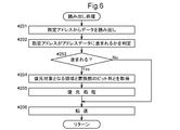
図6に示すように、読み出し処理では、指定されたアドレス領域(指定アドレス領域)からデータが読み出された場合には、指定アドレス領域が記憶回路15に記憶されているアドレスデータにより特定されるアドレスに該当するかの判定が行われる(#201、#202ステップ)。
図6に示すように、読み出し処理では、指定されたアドレス領域(指定アドレス領域)からデータが読み出された場合には、指定アドレス領域が記憶回路15に記憶されているアドレスデータにより特定されるアドレスに該当するかの判定が行われる(#201、#202ステップ)。
この処理では、メモリコントローラCに読み出しの要求があり、データリードユニット7aがメモリMからデータを読み出した場合には、データリードユニット7aで読み出したデータが復元モジュール21に与えられる。これと連係して、データリードユニット7aは、特定モジュール22に指定アドレスの情報を与え、特定モジュール22は、記憶回路15に記憶されているアドレスデータにより特定されるアドレスと比較する。この比較では、指定アドレスが、記憶回路15に記憶されているアドレスデータにより特定されるアドレスに該当するかの判定が行われる。
指定アドレスが記憶回路15に記憶されているアドレスデータにより特定されるアドレスに該当すると判定した場合には、特定モジュール22は、メモリMから読み出したデータのうち、対応するアドレスデータにより特定されるアドレスの情報と、当該アドレスデータに関連付けられている対象パターンの情報とを復元モジュール21に与える。これにより、復元モジュール21は、メモリMから読み出したデータを復元処理し、要求元に対して復元されたデータを転送する。また、復元が不要である場合には、取得したデータを、そのまま伝送する(#203~#206ステップ)。
ここでは、1つのデータ伝送レーンについての読み出し処理の形態を説明したが、当然のことながら、本実施形態のように、複数のデータ伝送レーン(DG1、DG2)を備える場合には、当該の複数のデータ伝送レーン(DG1、DG2)それぞれについて、この読み出し処理が行われる。
〔出現頻度テーブルの設定〕
出現頻度テーブル13は、信号ラインDLを介してメモリMに転送される転送データの「1」と「0」のビット列が予め設定された複数の対象パターンの何れかに含まれるかの判定と、含まれる場合には何れの対象パターンであるかの判定とに用いられる。この出現頻度テーブル13は、出現頻度の高いパターンと、出現頻度が低いパターンとを記憶したデータ構造を有している。
出現頻度テーブル13は、信号ラインDLを介してメモリMに転送される転送データの「1」と「0」のビット列が予め設定された複数の対象パターンの何れかに含まれるかの判定と、含まれる場合には何れの対象パターンであるかの判定とに用いられる。この出現頻度テーブル13は、出現頻度の高いパターンと、出現頻度が低いパターンとを記憶したデータ構造を有している。
この出現頻度は、図10に示すノイズ分析装置ANによって予め取得された出現頻度情報に基づいて設定される。前述したように、メモリコントローラCは、マイクロプロセッサやDSP等と同様にプログラムに従う処理を実現するものである。この構成を利用して、メモリコントローラCのプログラムを設定することで、図10に示すノイズ分析装置ANが構成される。このノイズ分析装置ANでは、専用のコンピュータ等が接続され、出力された出現頻度情報は、専用のコンピュータ等で取得され、出現頻度テーブル13に記憶されることになる。或いは、ノイズ分析装置AN自体が、出現頻度情報に基づいて、出現頻度テーブル13を生成したり、随時更新したりする構成とされても好適である。
本実施形態では、ノイズ分析装置ANは、データリード部31と、データライト部32と、パターン判定部33と、判定パターンテーブル34と、積算処理部35と、頻度出力部37と、デバイス識別部38と、出力タイミング設定部39とを備えている。ここで、パターン判定部33は、信号ラインDLを介してメモリMに読み書きされる伝送データのビット列の「1」と「0」の並びのパターンが、設定された少なくとも1つの判定パターンに合致するか否かを判定する。判定パターンテーブル34には、設定された少なくとも1つの判定パターンの情報、具体的には判定パターンのビット列が記憶されている。積算処理部35は、パターン判定部33で判定された判定パターンの出現回数を積算値として取得する。頻度出力部37は、積算処理部35により取得された積算値と、当該積算値が表す判定パターンを特定するパターン特定情報と、を関連付けた出現頻度情報を出力する。
このノイズ分析装置ANでは、各種のデバイスが、メモリMに記憶されたデータに対して現実にアクセスする場合に、信号ラインDLを伝送される「1」と「0」のビット列のパターンを取得し、各パターンの出現頻度を取得する。図11のフローチャートには、その処理の概要を示している。また、出現頻度情報を取得する対象は、分析対象として設定された少なくとも一つの判定パターンに合致する伝送データのビット列である。
つまり、データリード部31又はデータライト部32を介して、メモリMに読み書きされる伝送データのビット列が信号ラインDLを介して伝送された場合には、パターン判定部33が当該伝送データを取得し、判定パターンテーブル34のデータに基づき、設定された少なくとも一つの判定パターンに合致するか否かの判定を行う(#301~#303ステップ)。
次に、積算処理部35が、パターン判定部33で判定された判定パターンの出現回数を積算値として取得する。この際、積算処理部35は、パターン判定部33で判定パターンに合致すると判定された伝送データについて、その判定パターンを特定するパターン特定情報を取得し、判定パターン毎の出現回数を積算する。また、本実施形態では、積算処理部35は、メモリMにデータを書き込む場合と、メモリMからデータを読み出す場合とを区別して積算値を取得する。また、積算処理部35は、伝送データが書き込まれるメモリM内のアドレスが、メモリMの記憶領域の中にある複数の区分領域のいずれに属するかに応じて、当該区分領域毎に積算値を取得する。更に、積算処理部35は、伝送データの送信元のデバイスが、メモリMにアクセス可能な複数のデバイスの中の何れであるかに応じて、当該デバイス毎に積算値を取得する。そのために、積算処理部35は、パターン判定部33で判定パターンと判定された伝送データについて、アクセス情報と、区分領域情報と、デバイス情報と、を含む属性情報を取得する。そして、取得したパターン特定情報に、当該属性情報を関連付けて、各判定パターンの出現回数を積算し、積算値として取得する(#304~#306ステップ)。
図9は、積算処理部35が取得する、パターン特定情報と属性情報とに関連付けられた積算値データの一例を示している。同図に示すように複数種の判定パターンを識別するため、積算値データのそれぞれは、パターン特定情報をインデックスとしており、属性情報として、(R)と(W)とで示すアクセス情報、(A1~A3)で示す区分領域情報、(D1~D3)で示すデバイス情報、の各々を備えている。また、このパターン特定情報には、当該パターン特定情報により特定される判定パターンのビット列情報が関連付けられている。
具体的には、アクセス情報の(R)と(W)は、メモリMにデータ(ビット列情報)を書き込む場合(R)と、メモリMからデータ(ビット列情報)を読み出す場合(W)との区別を示している。区分領域情報の(A1~A3)は、判定パターンの伝送データ(ビット列情報)が書き込まれるメモリM内のアドレスが、メモリMの記憶領域の中にある複数の区分領域(A1~A3)のいずれに属するかを示している。デバイス情報の(D1~D3)は、判定パターンの伝送データ(ビット列情報)の送信元のデバイスが、メモリMにアクセス可能な複数のデバイス(D1~D3)の中の何れであるかを示している。ここで、送信元のデバイスが何れであるかは、デバイス識別部38により識別され、その識別情報が積算処理部36に与えられる。尚、区分領域情報は上記した3つの領域に限らず、デバイスの数も3つに限らない。
そして、積算処理部35は、パターン特定情報により特定された判定パターン毎、及び各属性情報毎に、出現回数を積算し、その積算値をインクリメントする(#306ステップ)。具体的には、メモリMに読み書きされる伝送データのビット列が判定パターンに合致する毎に、積算処理部35は、当該の伝送データ(ビット列情報)についてのパターン特定情報と、属性情報としての(R)と(W)とで示すアクセス情報、(A1~A3)で示す区分領域情報、及び(D1~D3)で示すデバイス情報を取得する。そして、積算処理部35は、当該取得した情報に応じて、図9に示すような、積算値データであって、当該判定パターンを特定するパターン特定情報を有するデータについて、アクセス情報の(R)と(W)の何れかの値をインクリメントし、区分領域情報の(A1~A3)の何れかの値をインクリメントし、デバイス情報の(D1~D3)の何れかの値をインクリメントする。
そして、頻度出力部37が、予め設定された出力タイミングで、出現頻度情報を出力する(#307、#308ステップ)。ここで、出現頻度情報は、積算処理部35により取得された積算値と、当該積算値が表す判定パターンを特定するパターン特定情報と、を関連付けた情報である。本実施形態では、出現頻度情報は、更に、アクセス情報と、区分領域情報と、デバイス情報と、を含む属性情報も、積算値及びパターン特定情報に関連付けた情報となっている。具体的には、頻度出力部37は、出力タイミングとなった時点での上記積算値データ(図9参照)を積算処理部35から取得し、その時点での積算値データを出現頻度情報として出力する。また、これらの#301~#308ステップの処理は、リセットされるまで反復して実行される(#309ステップ)。
出力タイミング設定部39は、設定された出力タイミングに従って、頻度出力部37に対して出力のトリガー情報を与える。頻度出力部37は、このトリガー情報に応じて出現頻度情報を出力する。本実施形態では、出力タイミング設定部39は、積算処理部35による積算値が予め設定した出力閾値を超える毎、又は当該積算値の積算期間が予め設定した出力期間を超える毎に、頻度出力部37に出力のトリガー情報を与える。具体的には、出力タイミング設定部39は、図9に示す積算値データの各項目の積算値の中でも最も値が大きいものが、予め設定した出力閾値を超える毎、又は、積算値データの積算値の積算期間が予め設定した出力期間を超える毎に、トリガー情報を頻度出力部37に対して出力する。尚、出力タイミング設定部39は、予め設定した出力閾値を超えるという値条件と、積算値データの積算値の積算期間が予め設定した出力期間を超えるという期間条件と、の双方を満たす毎にトリガー情報を出力する構成とされてもよい。
この分析処理により得られる出現頻度情報に基づいて、各属性情報の積算値をソートすることにより、アクセス情報と区分領域情報デバイス情報との何れか1つ又はこれらの組み合わせを基準にした出現頻度を得ることができる。
例えば、車載のカーナビゲーション機器等、メモリMが使用される機器によっては、メモリMの記憶領域が予め複数の区分領域に区分され、区分領域毎に異なる種類のデータが記憶される構成となっている場合がある。例えば、第1の区分領域には地図情報を記憶し、第2の区分領域には静止画像情報を記憶し、第
3の区分領域には音声情報を記憶し、第4の区分領域にはプログラムの情報を記憶する等、データ種別毎に記憶される区分領域が予め定まっている場合がある。同様に、メモリMに対してアクセス可能なデバイスが複数存在する場合であって、デバイス毎に異なる種類のデータが伝送される場合がある。例えば、メモリコントローラCを介してメモリMにアクセス可能に構成された複数のデバイスのうち、地図描画デバイスが地図データを伝送し、画像表示デバイスが静止画データを伝送し、オーディオ再生デバイスが音声情報を伝送し、演算処理デバイスがプログラムデータを伝送する等、メモリMにアクセスするデバイス毎に異なる種別のデータ伝送が行われる場合がある。そして、このようなデータ種別に応じて、メモリコントローラCとメモリMとの間で伝送されるデータのビット列の「1」と「0」との組み合せパターンの出現頻度にも偏りが生じ、その偏りに一定の傾向が現れる場合がある。従って、伝送データのビット列の中で出現頻度が高いパターンも、メモリMの中の区分領域毎、或いは、メモリMにアクセスするデバイス毎に異なる場合がある。
3の区分領域には音声情報を記憶し、第4の区分領域にはプログラムの情報を記憶する等、データ種別毎に記憶される区分領域が予め定まっている場合がある。同様に、メモリMに対してアクセス可能なデバイスが複数存在する場合であって、デバイス毎に異なる種類のデータが伝送される場合がある。例えば、メモリコントローラCを介してメモリMにアクセス可能に構成された複数のデバイスのうち、地図描画デバイスが地図データを伝送し、画像表示デバイスが静止画データを伝送し、オーディオ再生デバイスが音声情報を伝送し、演算処理デバイスがプログラムデータを伝送する等、メモリMにアクセスするデバイス毎に異なる種別のデータ伝送が行われる場合がある。そして、このようなデータ種別に応じて、メモリコントローラCとメモリMとの間で伝送されるデータのビット列の「1」と「0」との組み合せパターンの出現頻度にも偏りが生じ、その偏りに一定の傾向が現れる場合がある。従って、伝送データのビット列の中で出現頻度が高いパターンも、メモリMの中の区分領域毎、或いは、メモリMにアクセスするデバイス毎に異なる場合がある。
そこで、伝送データが書き込まれるアドレスが、メモリMの記憶領域の中にある複数の区分領域のいずれに属するかに応じて、或いは、伝送データの送信元のデバイスが、メモリMにアクセス可能な複数のデバイスの中のいずれであるかに応じて、対象パターン及び置換後パターンの少なくとも一方を異ならせると好適である。例えば、上述した出現頻度情報に基づいて、メモリMの区分領域毎の出現頻度を取得し、伝送データが書き込まれるアドレスが属する区分領域毎に、出現頻度が基準値Eより高いパターンの中の少なくとも一つを対象パターンに設定し、出現頻度が基準値Eより低いパターンの中の少なくとも一つを置換後パターンに設定するとよい。或いは、出現頻度情報に基づいて、伝送データの送信元のデバイス毎の出現頻度を取得し、伝送データの送信元のデバイス毎に、出現頻度が基準値Eより高いパターンの中の少なくとも一つを対象パターンに設定し、出現頻度が基準値Eより低いパターンの中の少なくとも一つを置換後パターンに設定してもよい。
2.その他の実施形態
(1)上記の実施形態では、複数のデータ伝送レーン(DG1、DG2)を備える場合に、データ伝送レーン(DG1、DG2)毎に1つの対象パターンと1つの置換後パターンを設定する場合を例として説明した。しかし、当然ながら、データ伝送レーン(DG1、DG2)毎に複数の対象パターンを設定すると共に、複数の対象パターンのそれぞれに対応して置換後パターンを設定しても好適である。当然ながら、データ伝送レーンが1つの場合に、複数の対象パターンと複数の置換後パターンを設定しても好適である。また、全てのデータ伝送レーン(DG1、DG2)について共通の1つ又は複数の対象パターンを設定してもよい。
(1)上記の実施形態では、複数のデータ伝送レーン(DG1、DG2)を備える場合に、データ伝送レーン(DG1、DG2)毎に1つの対象パターンと1つの置換後パターンを設定する場合を例として説明した。しかし、当然ながら、データ伝送レーン(DG1、DG2)毎に複数の対象パターンを設定すると共に、複数の対象パターンのそれぞれに対応して置換後パターンを設定しても好適である。当然ながら、データ伝送レーンが1つの場合に、複数の対象パターンと複数の置換後パターンを設定しても好適である。また、全てのデータ伝送レーン(DG1、DG2)について共通の1つ又は複数の対象パターンを設定してもよい。
(2)上記の実施形態では、データ伝送レーン(DG1、DG2)のそれぞれが、複数の信号ラインDLを備えている場合を例として説明した。しかし、当然ながら、データ伝送レーン(DG1、DG2)のそれぞれが、1本の信号ラインDLにより構成されていてもよい。すなわち、信号ラインDL毎に、対象パターンと置換後パターンを設定してもよい。
(3)上記の実施形態では、置換後パターンを、出現頻度が基準値Eより低いパターンの中から設定する場合を例として説明した。しかし、これ以外の構成とすることもできる。
例えば、置換後パターンを、「0」だけが連続するビット列、又は、「1」だけが連続するビット列としても好適である。このような置換後パターンを設定することにより、置換ビット列が、信号ラインDLにおいて全て同じ電位となるため、ノイズを有効に低減させることができる。また、このような置換後パターンを用いる場合、ノイズを発生させやすい複数のパターンの初期ビット列の全てを「0」又は「1」だけが連続する置換ビット列に置換することも可能となる。従って、置換ユニット6bでの処理を単純にして処理速度の向上を図ることも可能となる。
例えば、置換後パターンを、「0」だけが連続するビット列、又は、「1」だけが連続するビット列としても好適である。このような置換後パターンを設定することにより、置換ビット列が、信号ラインDLにおいて全て同じ電位となるため、ノイズを有効に低減させることができる。また、このような置換後パターンを用いる場合、ノイズを発生させやすい複数のパターンの初期ビット列の全てを「0」又は「1」だけが連続する置換ビット列に置換することも可能となる。従って、置換ユニット6bでの処理を単純にして処理速度の向上を図ることも可能となる。
(4)上記の実施形態では、対象パターンを、出現頻度が基準値Eより高いパターンの中の少なくとも1つに設定し、置換後パターンを、出現頻度が基準値Eより低いパターンの中の少なくとも1つに設定する場合について説明した。しかし、これに限定されず、対象パターン及び置換後パターンを、出現頻度以外の他の基準に基づいて設定してもよい。例えば、置換ユニット6bによる置き換え前のデータに含まれるビット列の「1」と「0」の並びのパターンが、予め定められたノイズ周波数域のノイズを発生させるパターンの中の少なくとも一つを、対象パターンに設定し、当該ノイズ周波数域のノイズを発生させるパターン以外のパターンの中の少なくとも一つを、置換後パターンに設定しても好適である。ノイズを低減したい周波数域が既に決まっている場合には、このような設定とすることで、有効にノイズを低減することができる。なお、低減したい周波数域のノイズを発生させるビット列のパターンが複数存在する場合には、それらの一部または全部のパターンを対象パターンに設定するとよい。
(5)上記実施形態では、頻度出力部37により出力される出現頻度情報が、積算値と、パターン特定情報と、属性情報とを関連付けた情報である場合を例として説明した。しかし、出現頻度情報が、積算値と、パターン特定情報と、を関連付けただけの情報であってもよい。また、上記の実施形態では、属性情報として、アクセス情報と、区分領域情報と、デバイス情報と、が含まれる場合を例として説明した。しかし、属性情報として、これらの一部のみが含まれる構成としてもよいし、これら以外の情報が含まれる構成としてもよい。
(6)なお、上述した各実施形態で開示された構成は、矛盾が生じない限り、他の実施形態で開示された構成と組み合わせて適用することも可能である。その他の構成に関しても、本明細書において開示された実施形態は全ての点で単なる例示に過ぎない。従って、本開示の趣旨を逸脱しない範囲内で、適宜、種々の改変を行うことが可能である。
3.上記実施形態の概要
以下、上記において説明したメモリコントローラの概要について説明する。
以下、上記において説明したメモリコントローラの概要について説明する。
メモリコントローラ(C)は、メモリ(M)のアドレスを指定し信号ライン(DL)を介してメモリ(M)にデータを書き込む書込部(6)と、前記メモリ(M)のアドレスを指定し前記信号ライン(DL)を介して前記メモリ(M)からデータを読み出す読出部(7)とを備え、
前記書込部(M)が、前記信号ライン(DL)を介して前記メモリ(M)に書き込まれる伝送データのビット列の「1」と「0」との並びが置換対象として設定された対象パターンである場合に、前記メモリ(M)に書き込む以前に、前記対象パターンの初期ビット列を、「1」と「0」との並びが前記対象パターンとは異なる置換後パターンとなる置換ビット列に置き換える置換ユニット(6b)を備え、
前記読出部(7)が、前記メモリ(M)から読み出したデータの前記置換ビット列を前記初期ビット列に復元する復元ユニット(7b)を備えている。
前記書込部(M)が、前記信号ライン(DL)を介して前記メモリ(M)に書き込まれる伝送データのビット列の「1」と「0」との並びが置換対象として設定された対象パターンである場合に、前記メモリ(M)に書き込む以前に、前記対象パターンの初期ビット列を、「1」と「0」との並びが前記対象パターンとは異なる置換後パターンとなる置換ビット列に置き換える置換ユニット(6b)を備え、
前記読出部(7)が、前記メモリ(M)から読み出したデータの前記置換ビット列を前記初期ビット列に復元する復元ユニット(7b)を備えている。
この構成によれば、対象パターン及び置換後パターンを適切に設定することにより、問題となるノイズを発生させるビット列のパターンを別のパターンに置き換えることができるため、メモリ(M)に対してデータを書き込む場合とメモリ(M)からデータを読み出す場合の双方において、信号ライン(DL)で発生するノイズを低減することが可能となる。
またこの際、ソフトウエア的に対象パターン及び置換後パターンの設定を変更するだけで様々な周波数のノイズを低減することができる。従って、例えば信号ライン(DL)を覆うシールドを設け、或いは、回路設計によりノイズ対策を行う場合に比べ、容易に低減対象のノイズ周波数を変更することができる。従って、メモリ(M)及びメモリコントローラ(C)の使用環境に応じて柔軟にノイズ対策を実施できる。
更に、この構成によれば、置換ユニット(6b)の機能と復元ユニット(7b)の機能とをメモリコントローラ(C)に装備させるだけでよく、メモリ(M)については一般的なものを使用することが可能である。ソフトウエア設定についても、メモリコントローラ(C)のみの設定で済むため、ソフトウエア設定手順を簡略化することが可能である。
また、前記置換ユニット(6b)が、
前記伝送データのビット列の「1」と「0」との並びが前記対象パターンであるかを判定するパターン判定モジュール(12)と、
前記パターン判定モジュール(12)で前記対象パターンであることを判定した場合に、前記初期ビット列を前記置換ビット列に置き換える置換モジュール(11)と、
前記置換モジュール(11)での置き換えを行った場合に、前記対象パターンと、前記置換ビット列が書き込まれる前記メモリ(M)のアドレスを特定するためのアドレスデータと、を関連付けて記憶させる記憶モジュール(14)と、を備え、
前記復元ユニット(7b)が、
前記アドレスデータに基づいて、前記メモリ(M)から読み出したデータの中に含まれる前記置換ビット列を特定する特定モジュール(22)と、
前記アドレスデータに関連付けられている前記対象パターンに基づいて、前記置換ビット列を置き換え前の前記初期ビット列に復元する復元モジュール(21)と、を備えると好適である。
この構成によれば、メモリ(M)に書き込まれる伝送データが対象パターンであることをパターン判定モジュール(12)が判定した場合には、置換モジュール(11)が、対象パターンの初期ビット列を置換ビット列に置き換え、このように書き換えられた置換ビット列がメモリ(M)に書き込まれる。また、置き換え時には、対象パターンとアドレスデータとが関連付けられて記憶モジュール(14)により所定の記憶部等に記憶される。
この後にメモリ(M)から読み出されたデータに置換ビット列が含まれることを、特定モジュール(22)が判定した場合には、その置換ビット列が復元モジュール(21)で初期ビット列に復元される。
この後にメモリ(M)から読み出されたデータに置換ビット列が含まれることを、特定モジュール(22)が判定した場合には、その置換ビット列が復元モジュール(21)で初期ビット列に復元される。
また、前記置換ユニット(6b)による置き換え前のデータに含まれるビット列の「1」と「0」の並びのパターンの出現頻度が、予め定められた基準値(E)よりも高いパターンの中の少なくとも一つを、前記対象パターンに設定し、
前記出現頻度が、前記基準値(E)よりも低いパターンの中の少なくとも一つを、前記置換後パターンに設定すると好適である。
前記出現頻度が、前記基準値(E)よりも低いパターンの中の少なくとも一つを、前記置換後パターンに設定すると好適である。
この構成によれば、出現頻度が基準値(E)より高いビット列のパターンを、出現頻度が基準値(E)より低いパターンのビット列に置き換えて信号ライン(DL)を伝送させることができる。従って、出現頻度が高いためにノイズを発生させる可能性が高いビット列のパターンを少なくすることができ、信号ライン(DL)で発生するノイズを低減することが可能となる。
或いは、前記置換ユニット(6b)による置き換え前のデータに含まれるビット列の「1」と「0」の並びのパターンが、予め定められたノイズ周波数域のノイズを発生させるパターンの中の少なくとも一つを、前記対象パターンに設定し、
前記ノイズ周波数域のノイズを発生させるパターン以外のパターンの中の少なくとも一つを、前記置換後パターンに設定すると好適である。
前記ノイズ周波数域のノイズを発生させるパターン以外のパターンの中の少なくとも一つを、前記置換後パターンに設定すると好適である。
この構成によれば、予め定められたノイズ周波数域のノイズを発生させるビット列のパターンを、当該周波数域のノイズを発生させないパターンのビット列に置き換えて信号ライン(DL)を伝送させることができる。従って、低減させたい特定周波数域のノイズを発生させるビット列のパターンを少なくすることができ、信号ライン(DL)で発生する当該特定周波数域のノイズを低減することが可能となる。ノイズを低減したい周波数域が既に決まっている場合には、このような設定とすることで、有効にノイズを低減することができる。
また、前記信号ライン(DL)を複数備えると共に、複数の前記信号ライン(DL)により第1伝送レーン(DG1)と第2伝送レーン(DG2)とを少なくとも含む複数のデータ伝送レーンが構成され、
前記置換ユニット(6b)は、前記第1伝送レーン(DG1)を介して伝送される前記置換ビット列の「1」と「0」との並びにより生じるオンオフ周波数と、前記第2伝送レーンを介して伝送される前記置換ビット列の「1」と「0」との並びにより生じるオンオフ周波数とが異なるように、前記第1伝送レーン(DG1)と前記第2伝送レーン(DG2)とで異なる前記置換後パターンを設定すると好適である。
前記置換ユニット(6b)は、前記第1伝送レーン(DG1)を介して伝送される前記置換ビット列の「1」と「0」との並びにより生じるオンオフ周波数と、前記第2伝送レーンを介して伝送される前記置換ビット列の「1」と「0」との並びにより生じるオンオフ周波数とが異なるように、前記第1伝送レーン(DG1)と前記第2伝送レーン(DG2)とで異なる前記置換後パターンを設定すると好適である。
この構成によれば、複数のデータ伝送レーンにおける置換ビット列のオンオフ周波数を分散させることができるので、置換ユニット(6b)による置換処理によって特定の周波数のノイズが増加することを抑制できる。
また、前記信号ライン(DL)を複数備えると共に、複数の前記信号ライン(DL)により第1伝送レーン(DG1)と第2伝送レーン(DG2)とを少なくとも含む複数のデータ伝送レーンが構成され、
前記置換ユニット(6b)は、前記第1伝送レーン(DG1)を介して伝送される前記置換ビット列の「1」と「0」との境界のタイミングと、前記第2伝送レーン(DG2)を介して伝送される前記置換ビット列の「1」と「0」との境界のタイミングとが異なるように、前記第1伝送レーン(DG1)と前記第2伝送レーン(DG2)とで異なる前記置換後パターンを設定すると好適である。
前記置換ユニット(6b)は、前記第1伝送レーン(DG1)を介して伝送される前記置換ビット列の「1」と「0」との境界のタイミングと、前記第2伝送レーン(DG2)を介して伝送される前記置換ビット列の「1」と「0」との境界のタイミングとが異なるように、前記第1伝送レーン(DG1)と前記第2伝送レーン(DG2)とで異なる前記置換後パターンを設定すると好適である。
この構成によれば、置換ユニット(6b)による置換処理の後、複数のデータ伝送レーン(DG1、DG2)での置換後ビット列の「1」と「0」との境界のタイミングが同じになることに起因して、当該タイミングでノイズが増加することを抑制できる。
前記書込部(6)は、前記伝送データが書き込まれる前記アドレスが、前記メモリ(M)の記憶領域の中にある複数の区分領域のいずれに属するかに応じて、或いは、前記伝送データの送信元のデバイスが、前記メモリ(M)にアクセス可能な複数のデバイスの中のいずれであるかに応じて、前記対象パターン及び前記置換後パターンの少なくとも一方を異ならせると好適である。
メモリ(M)が使用される機器によっては、メモリ(M)の記憶領域が予め複数の区分領域に区分され、区分領域毎に異なる種類のデータが記憶される構成となっている場合がある。また、メモリ(M)に対してアクセス可能なデバイスが複数存在する場合であって、デバイス毎に異なる種類のデータが伝送される場合がある。そして、このようなデータ種別に応じて、メモリコントローラ(C)とメモリ(M)との間で伝送されるデータのビット列の「1」と「0」との組み合せパターンの出現頻度にも偏りが生じ、その偏りに一定の傾向が現れる場合がある。従って、伝送データのビット列の中で出現頻度が高いパターンも、メモリ(M)の中の区分領域毎、或いは、メモリ(M)にアクセスするデバイス毎に異なる場合がある。上記の構成によれば、このようなデータ種別毎の偏りに応じて、対象パターン及び置換後パターンの少なくとも一方を適切に設定することができる。従って、信号ライン(DL)で発生するノイズを効果的に低減することができる。
また、前記置換後パターンが、「0」だけが連続するビット列、又は、「1」だけが連続するビット列であっても好適である。
この構成によれば、置換ビット列が、信号ライン(DL)において全て同じ電位となるため、ノイズを有効に低減させることができる。また、このような置換後パターンを用いる場合、ノイズを発生させやすい複数のパターンの初期ビット列の全てを「0」又は「1」だけが連続する置換ビット列に置換することも可能となる。従って、置換ユニット(6b)での処理を単純にして処理速度の向上を図ることも可能となる。
本開示に係る技術は、メモリに対して信号ラインを介してデータ伝送を行うメモリコントローラに利用することができる。
6 書込部
6b 置換ユニット
7 読出部
7b 復元ユニット
11 置換モジュール
12 パターン判定モジュール
14 記憶処理モジュール
21 復元モジュール
D データバス
DL 信号ライン
DG1 第1伝送レーン
DG2 第2伝送レーン
E 基準値
M メモリ
6b 置換ユニット
7 読出部
7b 復元ユニット
11 置換モジュール
12 パターン判定モジュール
14 記憶処理モジュール
21 復元モジュール
D データバス
DL 信号ライン
DG1 第1伝送レーン
DG2 第2伝送レーン
E 基準値
M メモリ
Claims (8)
- メモリのアドレスを指定し信号ラインを介してメモリにデータを書き込む書込部と、前記メモリのアドレスを指定し前記信号ラインを介して前記メモリからデータを読み出す読出部とを備え、
前記書込部が、前記信号ラインを介して前記メモリに書き込まれる伝送データのビット列の「1」と「0」との並びが置換対象として設定された対象パターンである場合に、前記メモリに書き込む以前に、前記対象パターンの初期ビット列を、「1」と「0」との並びが前記対象パターンとは異なる置換後パターンとなる置換ビット列に置き換える置換ユニットを備え、
前記読出部が、前記メモリから読み出したデータの前記置換ビット列を前記初期ビット列に復元する復元ユニットを備えているメモリコントローラ。 - 前記置換ユニットが、
前記伝送データのビット列の「1」と「0」との並びが前記対象パターンであるかを判定するパターン判定モジュールと、
前記パターン判定モジュールで前記対象パターンであることを判定した場合に、前記初期ビット列を前記置換ビット列に置き換える置換モジュールと、
前記置換モジュールでの置き換えを行った場合に、前記対象パターンと、前記置換ビット列が書き込まれる前記メモリのアドレスを特定するためのアドレスデータと、を関連付けて記憶させる記憶モジュールと、を備え、
前記復元ユニットが、
前記アドレスデータに基づいて、前記メモリから読み出したデータの中に含まれる前記置換ビット列を特定する特定モジュールと、
前記アドレスデータに関連付けられている前記対象パターンに基づいて、前記置換ビット列を置き換え前の前記初期ビット列に復元する復元モジュールと、を備えている請求項1に記載のメモリコントローラ。 - 前記置換ユニットによる置き換え前のデータに含まれるビット列の「1」と「0」の並びのパターンの出現頻度が、予め定められた基準値よりも高いパターンの中の少なくとも一つを、前記対象パターンに設定し、
前記出現頻度が、前記基準値よりも低いパターンの中の少なくとも一つを、前記置換後パターンに設定している請求項1又は2に記載のメモリコントローラ。 - 前記置換ユニットによる置き換え前のデータに含まれるビット列の「1」と「0」の並びのパターンが、予め定められたノイズ周波数域のノイズを発生させるパターンの中の少なくとも一つを、前記対象パターンに設定し、
前記ノイズ周波数域のノイズを発生させるパターン以外のパターンの中の少なくとも一つを、前記置換後パターンに設定している請求項1又は2に記載のメモリコントローラ。 - 前記信号ラインを複数備えると共に、複数の前記信号ラインにより第1伝送レーンと第2伝送レーンとを少なくとも含む複数のデータ伝送レーンが構成され、
前記置換ユニットは、前記第1伝送レーンを介して伝送される前記置換ビット列の「1」と「0」との並びにより生じるオンオフ周波数と、前記第2伝送レーンを介して伝送される前記置換ビット列の「1」と「0」との並びにより生じるオンオフ周波数とが異なるように、前記第1伝送レーンと前記第2伝送レーンとで異なる前記置換後パターンを設定している請求項1から4のいずれか一項に記載のメモリコントローラ。 - 前記信号ラインを複数備えると共に、複数の前記信号ラインにより第1伝送レーンと第2伝送レーンとを少なくとも含む複数のデータ伝送レーンが構成され、
前記置換ユニットは、前記第1伝送レーンを介して伝送される前記置換ビット列の「1」と「0」との境界のタイミングと、前記第2伝送レーンを介して伝送される前記置換ビット列の「1」と「0」との境界のタイミングとが異なるように、前記第1伝送レーンと前記第2伝送レーンとで異なる前記置換後パターンを設定している請求項1から4のいずれか一項に記載のメモリコントローラ。 - 前記書込部は、前記伝送データが書き込まれる前記アドレスが、前記メモリの記憶領域の中にある複数の区分領域のいずれに属するかに応じて、或いは、前記伝送データの送信元のデバイスが、前記メモリにアクセス可能な複数のデバイスの中のいずれであるかに応じて、前記対象パターン及び前記置換後パターンの少なくとも一方を異ならせている請求項1から6のいずれか一項に記載のメモリコントローラ。
- 前記置換後パターンが、「0」だけが連続するビット列、又は、「1」だけが連続するビット列である請求項1から7のいずれか一項に記載のメモリコントローラ。
Priority Applications (3)
| Application Number | Priority Date | Filing Date | Title |
|---|---|---|---|
| US15/552,337 US20180024747A1 (en) | 2015-03-25 | 2016-03-24 | Memory controller |
| CN201680016795.2A CN107408066B (zh) | 2015-03-25 | 2016-03-24 | 存储器控制器 |
| EP16768908.2A EP3242211B1 (en) | 2015-03-25 | 2016-03-24 | Memory controller |
Applications Claiming Priority (2)
| Application Number | Priority Date | Filing Date | Title |
|---|---|---|---|
| JP2015063178A JP6414497B2 (ja) | 2015-03-25 | 2015-03-25 | メモリコントローラ |
| JP2015-063178 | 2015-03-25 |
Publications (1)
| Publication Number | Publication Date |
|---|---|
| WO2016153005A1 true WO2016153005A1 (ja) | 2016-09-29 |
Family
ID=56977612
Family Applications (1)
| Application Number | Title | Priority Date | Filing Date |
|---|---|---|---|
| PCT/JP2016/059472 Ceased WO2016153005A1 (ja) | 2015-03-25 | 2016-03-24 | メモリコントローラ |
Country Status (5)
| Country | Link |
|---|---|
| US (1) | US20180024747A1 (ja) |
| EP (1) | EP3242211B1 (ja) |
| JP (1) | JP6414497B2 (ja) |
| CN (1) | CN107408066B (ja) |
| WO (1) | WO2016153005A1 (ja) |
Families Citing this family (1)
| Publication number | Priority date | Publication date | Assignee | Title |
|---|---|---|---|---|
| JP7211273B2 (ja) | 2019-06-17 | 2023-01-24 | 株式会社アイシン | 半導体記憶装置 |
Citations (2)
| Publication number | Priority date | Publication date | Assignee | Title |
|---|---|---|---|---|
| JP2008102705A (ja) * | 2006-10-18 | 2008-05-01 | Canon Inc | メモリアクセス制御回路及びその方法 |
| WO2012120813A1 (ja) * | 2011-03-08 | 2012-09-13 | ルネサスエレクトロニクス株式会社 | ビットパターン逆置換装置、コンピュータ装置、ビットパターン置換装置、ライタ装置、ビットパターン変換方法、及びプログラム |
Family Cites Families (13)
| Publication number | Priority date | Publication date | Assignee | Title |
|---|---|---|---|---|
| JP2004096376A (ja) * | 2002-08-30 | 2004-03-25 | Matsushita Electric Ind Co Ltd | データ圧縮方法、データ通信方法および半導体装置 |
| JP4921080B2 (ja) * | 2006-09-01 | 2012-04-18 | キヤノン株式会社 | メモリ制御回路及びメモリ制御方法 |
| JP5233165B2 (ja) * | 2007-05-24 | 2013-07-10 | 富士ゼロックス株式会社 | データ伝送装置 |
| JP2011015322A (ja) * | 2009-07-06 | 2011-01-20 | Renesas Electronics Corp | 半導体装置 |
| JP5650497B2 (ja) * | 2010-10-29 | 2015-01-07 | パナソニック株式会社 | リフレッシュ制御装置、無線受信機および半導体集積回路 |
| JP2012128778A (ja) * | 2010-12-17 | 2012-07-05 | Sony Corp | データ転送装置、メモリ制御装置、およびメモリシステム |
| US8666068B2 (en) * | 2011-10-20 | 2014-03-04 | Sandisk Technologies Inc. | Method for scrambling shaped data |
| WO2014010763A1 (ko) * | 2012-07-11 | 2014-01-16 | 한양대학교 산학협력단 | 쓰기 데이터 패턴 인식에 의한 플래시 메모리 관리 장치 및 방법 |
| US9311181B2 (en) * | 2012-11-15 | 2016-04-12 | Samsung Electronics Co., Ltd. | Memory controller changing partial data in memory device and method for changing partial data thereof |
| CN103019873B (zh) * | 2012-12-03 | 2016-08-10 | 华为技术有限公司 | 一种存储器故障单元的替换方法及装置、数据存储系统 |
| JP6317550B2 (ja) * | 2013-07-03 | 2018-04-25 | 株式会社メガチップス | Emi対策回路 |
| JP6398801B2 (ja) * | 2015-03-09 | 2018-10-03 | 沖電気工業株式会社 | メモリ装置へのデータ書き込み/読み出し制御方法及びメモリ装置 |
| JP6394458B2 (ja) * | 2015-03-25 | 2018-09-26 | アイシン・エィ・ダブリュ株式会社 | ノイズ分析装置およびメモリコントローラ |
-
2015
- 2015-03-25 JP JP2015063178A patent/JP6414497B2/ja not_active Expired - Fee Related
-
2016
- 2016-03-24 CN CN201680016795.2A patent/CN107408066B/zh not_active Expired - Fee Related
- 2016-03-24 EP EP16768908.2A patent/EP3242211B1/en not_active Not-in-force
- 2016-03-24 WO PCT/JP2016/059472 patent/WO2016153005A1/ja not_active Ceased
- 2016-03-24 US US15/552,337 patent/US20180024747A1/en not_active Abandoned
Patent Citations (2)
| Publication number | Priority date | Publication date | Assignee | Title |
|---|---|---|---|---|
| JP2008102705A (ja) * | 2006-10-18 | 2008-05-01 | Canon Inc | メモリアクセス制御回路及びその方法 |
| WO2012120813A1 (ja) * | 2011-03-08 | 2012-09-13 | ルネサスエレクトロニクス株式会社 | ビットパターン逆置換装置、コンピュータ装置、ビットパターン置換装置、ライタ装置、ビットパターン変換方法、及びプログラム |
Non-Patent Citations (1)
| Title |
|---|
| See also references of EP3242211A4 * |
Also Published As
| Publication number | Publication date |
|---|---|
| CN107408066A (zh) | 2017-11-28 |
| US20180024747A1 (en) | 2018-01-25 |
| EP3242211B1 (en) | 2018-11-21 |
| EP3242211A1 (en) | 2017-11-08 |
| JP6414497B2 (ja) | 2018-10-31 |
| EP3242211A4 (en) | 2017-12-27 |
| CN107408066B (zh) | 2020-10-23 |
| JP2016184233A (ja) | 2016-10-20 |
Similar Documents
| Publication | Publication Date | Title |
|---|---|---|
| CN114860329B (zh) | 动态一致性偏置配置引擎及方法 | |
| US10387305B2 (en) | Techniques for compression memory coloring | |
| US8583856B2 (en) | Memory system | |
| US8868844B2 (en) | System and method for a software managed cache in a multiprocessing environment | |
| KR20150022630A (ko) | 스토리지 디바이스 및 데이터 처리 방법 | |
| JP2004280752A (ja) | データ記憶装置、およびデータ記憶装置における管理情報更新方法、並びにコンピュータ・プログラム | |
| US20170300507A1 (en) | Computer readable recording medium, index generation device and index generation method | |
| CN111857552A (zh) | 存储管理方法、电子设备和计算机程序产品 | |
| US11307991B2 (en) | Apparatus and method and computer program product for generating a storage mapping table | |
| JP5658336B1 (ja) | ストアマージ処理装置、ストアマージ処理システム、ストアマージ処理方法、及び、ストアマージ処理プログラム | |
| JP6414497B2 (ja) | メモリコントローラ | |
| JP6394458B2 (ja) | ノイズ分析装置およびメモリコントローラ | |
| KR102628851B1 (ko) | 반도체 장치 및 그것을 구비한 반도체 시스템 | |
| US20130238881A1 (en) | Data transmission device, data transmission method, and computer program product | |
| US20220226735A1 (en) | Information processing device | |
| JP5953808B2 (ja) | 乱数処理装置、乱数処理方法、及びプログラム | |
| US20170039110A1 (en) | Computer | |
| WO2017087002A1 (en) | Shared memory for distributed data | |
| KR20240014431A (ko) | 스토리지 장치를 위한 적응형 캐시 인덱싱 | |
| CN111061724B (zh) | 用于配电自动化系统的高速实时数据库管理方法和装置 | |
| US20170278569A1 (en) | Duo Content Addressable Memory (CAM) Using A Single CAM | |
| US12499245B2 (en) | Methods and apparatus for selective encryption of execute in place (XIP) data | |
| WO2020039927A1 (ja) | 不揮発性記憶装置、ホスト装置、及びデータ記憶システム | |
| JP7168731B1 (ja) | メモリアクセス制御装置、メモリアクセス制御方法、及び、メモリアクセス制御プログラム | |
| US20150012492A1 (en) | Method and apparatus for replicating data |
Legal Events
| Date | Code | Title | Description |
|---|---|---|---|
| 121 | Ep: the epo has been informed by wipo that ep was designated in this application |
Ref document number: 16768908 Country of ref document: EP Kind code of ref document: A1 |
|
| REEP | Request for entry into the european phase |
Ref document number: 2016768908 Country of ref document: EP |
|
| WWE | Wipo information: entry into national phase |
Ref document number: 15552337 Country of ref document: US |
|
| NENP | Non-entry into the national phase |
Ref country code: DE |