WO2016157554A1 - 電磁波シールド材 - Google Patents
電磁波シールド材 Download PDFInfo
- Publication number
- WO2016157554A1 WO2016157554A1 PCT/JP2015/067662 JP2015067662W WO2016157554A1 WO 2016157554 A1 WO2016157554 A1 WO 2016157554A1 JP 2015067662 W JP2015067662 W JP 2015067662W WO 2016157554 A1 WO2016157554 A1 WO 2016157554A1
- Authority
- WO
- WIPO (PCT)
- Prior art keywords
- thickness
- insulating layer
- metal foil
- shielding material
- electromagnetic
- Prior art date
- Legal status (The legal status is an assumption and is not a legal conclusion. Google has not performed a legal analysis and makes no representation as to the accuracy of the status listed.)
- Ceased
Links
Classifications
-
- H—ELECTRICITY
- H05—ELECTRIC TECHNIQUES NOT OTHERWISE PROVIDED FOR
- H05K—PRINTED CIRCUITS; CASINGS OR CONSTRUCTIONAL DETAILS OF ELECTRIC APPARATUS; MANUFACTURE OF ASSEMBLAGES OF ELECTRICAL COMPONENTS
- H05K9/00—Screening of apparatus or components against electric or magnetic fields
- H05K9/0073—Shielding materials
- H05K9/0081—Electromagnetic shielding materials, e.g. EMI, RFI shielding
- H05K9/0084—Electromagnetic shielding materials, e.g. EMI, RFI shielding comprising a single continuous metallic layer on an electrically insulating supporting structure, e.g. metal foil, film, plating coating, electro-deposition, vapour-deposition
-
- B—PERFORMING OPERATIONS; TRANSPORTING
- B32—LAYERED PRODUCTS
- B32B—LAYERED PRODUCTS, i.e. PRODUCTS BUILT-UP OF STRATA OF FLAT OR NON-FLAT, e.g. CELLULAR OR HONEYCOMB, FORM
- B32B15/00—Layered products comprising a layer of metal
- B32B15/04—Layered products comprising a layer of metal comprising metal as the main or only constituent of a layer, which is next to another layer of the same or of a different material
- B32B15/08—Layered products comprising a layer of metal comprising metal as the main or only constituent of a layer, which is next to another layer of the same or of a different material of synthetic resin
-
- C—CHEMISTRY; METALLURGY
- C23—COATING METALLIC MATERIAL; COATING MATERIAL WITH METALLIC MATERIAL; CHEMICAL SURFACE TREATMENT; DIFFUSION TREATMENT OF METALLIC MATERIAL; COATING BY VACUUM EVAPORATION, BY SPUTTERING, BY ION IMPLANTATION OR BY CHEMICAL VAPOUR DEPOSITION, IN GENERAL; INHIBITING CORROSION OF METALLIC MATERIAL OR INCRUSTATION IN GENERAL
- C23C—COATING METALLIC MATERIAL; COATING MATERIAL WITH METALLIC MATERIAL; SURFACE TREATMENT OF METALLIC MATERIAL BY DIFFUSION INTO THE SURFACE, BY CHEMICAL CONVERSION OR SUBSTITUTION; COATING BY VACUUM EVAPORATION, BY SPUTTERING, BY ION IMPLANTATION OR BY CHEMICAL VAPOUR DEPOSITION, IN GENERAL
- C23C28/00—Coating for obtaining at least two superposed coatings either by methods not provided for in a single one of groups C23C2/00 - C23C26/00 or by combinations of methods provided for in subclasses C23C and C25C or C25D
-
- C—CHEMISTRY; METALLURGY
- C23—COATING METALLIC MATERIAL; COATING MATERIAL WITH METALLIC MATERIAL; CHEMICAL SURFACE TREATMENT; DIFFUSION TREATMENT OF METALLIC MATERIAL; COATING BY VACUUM EVAPORATION, BY SPUTTERING, BY ION IMPLANTATION OR BY CHEMICAL VAPOUR DEPOSITION, IN GENERAL; INHIBITING CORROSION OF METALLIC MATERIAL OR INCRUSTATION IN GENERAL
- C23C—COATING METALLIC MATERIAL; COATING MATERIAL WITH METALLIC MATERIAL; SURFACE TREATMENT OF METALLIC MATERIAL BY DIFFUSION INTO THE SURFACE, BY CHEMICAL CONVERSION OR SUBSTITUTION; COATING BY VACUUM EVAPORATION, BY SPUTTERING, BY ION IMPLANTATION OR BY CHEMICAL VAPOUR DEPOSITION, IN GENERAL
- C23C8/00—Solid state diffusion of only non-metal elements into metallic material surfaces; Chemical surface treatment of metallic material by reaction of the surface with a reactive gas, leaving reaction products of surface material in the coating, e.g. conversion coatings, passivation of metals
- C23C8/06—Solid state diffusion of only non-metal elements into metallic material surfaces; Chemical surface treatment of metallic material by reaction of the surface with a reactive gas, leaving reaction products of surface material in the coating, e.g. conversion coatings, passivation of metals using gases
- C23C8/08—Solid state diffusion of only non-metal elements into metallic material surfaces; Chemical surface treatment of metallic material by reaction of the surface with a reactive gas, leaving reaction products of surface material in the coating, e.g. conversion coatings, passivation of metals using gases only one element being applied
- C23C8/10—Oxidising
-
- H—ELECTRICITY
- H05—ELECTRIC TECHNIQUES NOT OTHERWISE PROVIDED FOR
- H05K—PRINTED CIRCUITS; CASINGS OR CONSTRUCTIONAL DETAILS OF ELECTRIC APPARATUS; MANUFACTURE OF ASSEMBLAGES OF ELECTRICAL COMPONENTS
- H05K9/00—Screening of apparatus or components against electric or magnetic fields
-
- H—ELECTRICITY
- H05—ELECTRIC TECHNIQUES NOT OTHERWISE PROVIDED FOR
- H05K—PRINTED CIRCUITS; CASINGS OR CONSTRUCTIONAL DETAILS OF ELECTRIC APPARATUS; MANUFACTURE OF ASSEMBLAGES OF ELECTRICAL COMPONENTS
- H05K9/00—Screening of apparatus or components against electric or magnetic fields
- H05K9/0073—Shielding materials
-
- B—PERFORMING OPERATIONS; TRANSPORTING
- B32—LAYERED PRODUCTS
- B32B—LAYERED PRODUCTS, i.e. PRODUCTS BUILT-UP OF STRATA OF FLAT OR NON-FLAT, e.g. CELLULAR OR HONEYCOMB, FORM
- B32B2250/00—Layers arrangement
- B32B2250/05—5 or more layers
-
- B—PERFORMING OPERATIONS; TRANSPORTING
- B32—LAYERED PRODUCTS
- B32B—LAYERED PRODUCTS, i.e. PRODUCTS BUILT-UP OF STRATA OF FLAT OR NON-FLAT, e.g. CELLULAR OR HONEYCOMB, FORM
- B32B2250/00—Layers arrangement
- B32B2250/42—Alternating layers, e.g. ABAB(C), AABBAABB(C)
-
- B—PERFORMING OPERATIONS; TRANSPORTING
- B32—LAYERED PRODUCTS
- B32B—LAYERED PRODUCTS, i.e. PRODUCTS BUILT-UP OF STRATA OF FLAT OR NON-FLAT, e.g. CELLULAR OR HONEYCOMB, FORM
- B32B2307/00—Properties of the layers or laminate
- B32B2307/20—Properties of the layers or laminate having particular electrical or magnetic properties, e.g. piezoelectric
- B32B2307/206—Insulating
-
- B—PERFORMING OPERATIONS; TRANSPORTING
- B32—LAYERED PRODUCTS
- B32B—LAYERED PRODUCTS, i.e. PRODUCTS BUILT-UP OF STRATA OF FLAT OR NON-FLAT, e.g. CELLULAR OR HONEYCOMB, FORM
- B32B2457/00—Electrical equipment
Definitions
- the present invention relates to an electromagnetic shielding material.
- the present invention relates to a covering material or an exterior material for an electric / electronic device.
- electromagnetic waves are radiated not only from automobiles but also from many electric / electronic devices including communication devices, displays and medical devices. Electromagnetic waves can cause malfunction of precision equipment, and there is also concern about the effects on the human body. For this reason, various techniques for reducing the influence of electromagnetic waves using electromagnetic shielding materials have been developed.
- a copper foil composite formed by laminating a copper foil and a resin film is used as an electromagnetic shielding material (Japanese Patent Laid-Open No. 7-290449).
- the copper foil has electromagnetic shielding properties, and the resin film is laminated for reinforcing the copper foil.
- An electromagnetic wave shield structure in which metal layers are laminated on the inner side and the outer side of an intermediate layer made of an insulating material (Japanese Patent No. 4602680).
- An electromagnetic wave shielding optical member comprising: a base substrate; and a laminated member formed on one surface of the base substrate and including a plurality of repeating unit films including a metal layer and a high refractive index layer (niobium pentoxide).
- niobium pentoxide high refractive index layer
- the present invention was created in view of the above circumstances, and has an object to provide an electromagnetic wave shielding material excellent in electromagnetic wave shielding characteristics, light weight characteristics, and molding processability, and in particular, a covering material for electric / electronic equipment or It is an object to provide an electromagnetic wave shielding material suitable as an exterior material.
- the present inventor made extensive studies to solve the above problems, and found that the electromagnetic wave shielding effect was remarkably improved by laminating three or more metal foils through an insulating layer. And it discovered that the electromagnetic wave shielding effect especially excellent was shown by combining suitably the electrical conductivity and thickness of metal foil, and the thickness of an insulating layer in this case.
- This invention is completed based on the said knowledge, and can be specified as follows.
- An electromagnetic wave shielding material having a structure in which at least three metal foils are laminated via an insulating layer, and all combinations of the metal foil and the insulating layer constituting the electromagnetic wave shielding material are ⁇ M ⁇ d M ⁇ d
- An electromagnetic shielding material satisfying R ⁇ 3 ⁇ 10 ⁇ 3 R ⁇ 3 ⁇ 10 ⁇ 3 .
- the symbol in a formula shows the following.
- ⁇ M conductivity of metal foil at 20 ° C.
- d M Metal foil thickness (m)
- R thickness of insulating layer (m)
- the electrical conductivity of each metal foil at 20 ° C. is 1.0 ⁇ 10 6 S / m or more.
- the thickness of each metal foil is 4 to 100 ⁇ m.
- the relative dielectric constant at 20 ° C. of each insulating layer is 2.0 to 10.0.
- the thickness of each insulating layer is 4 to 500 ⁇ m.
- the total thickness of the metal foil is 15 to 150 ⁇ m.
- the present invention is a covering material or an exterior material for an electric / electronic device provided with the electromagnetic wave shielding material according to the present invention.
- the present invention is an electric / electronic device including the covering material or the exterior material according to the present invention.
- the electromagnetic wave shielding material according to the present invention an excellent electromagnetic wave shielding effect is obtained while reducing the total thickness of the metal foil to be used by laminating three or more metal foils under a predetermined condition through an insulating layer. It becomes possible. Thereby, weight reduction can be achieved and molding processability can be secured. Moreover, the electromagnetic wave shielding material according to the present invention can be constructed with a simple configuration of a metal foil and an insulating layer, and is excellent in economic efficiency.
- Metal foil Although there is no restriction
- Such metals include iron conductivity of about 9.9 ⁇ 10 6 S / m, the conductivity of about 14.5 ⁇ 10 6 S / m of nickel, the conductivity of about 39.6 ⁇ 10 6 S Aluminum having a conductivity of about 58.0 ⁇ 10 6 S / m, and silver having a conductivity of about 61.4 ⁇ 10 6 S / m. In consideration of both electrical resistivity and cost, it is preferable in practical use to use aluminum or copper. All the metal foils used in the electromagnetic wave shielding material according to the present invention may be the same metal, or different metals may be used for each layer. Moreover, the metal alloy mentioned above can also be used. Various surface treatment layers for the purpose of adhesion promotion, environmental resistance, heat resistance and rust prevention may be formed on the surface of the metal foil.
- Au plating, Ag plating, Sn plating, Ni plating, Zn plating, Sn alloy plating (Sn—Ag) for the purpose of improving the environmental resistance and heat resistance required when the metal surface is the outermost layer.
- Sn—Ni, Sn—Cu, etc. Sn—Ni, Sn—Cu, etc.
- chromate treatment Sn plating or Sn alloy plating is preferable.
- chromate treatment roughening treatment, Ni plating and the like can be performed. These processes may be combined. Roughening treatment is preferable because adhesion can be easily obtained.
- a metal layer having a high relative permeability can be provided for the purpose of enhancing the shielding effect against a DC magnetic field.
- the metal layer having a high relative magnetic permeability include Fe—Ni alloy plating and Ni plating.
- the shielding performance improves, a thing with high purity is preferable, and purity is preferably 99.5 mass% or more, More preferably, it is 99.8 mass% or more.
- a rolled copper foil, an electrolytic copper foil, a copper foil by metallization, or the like can be used, and a rolled copper foil excellent in flexibility and moldability is preferable.
- alloy elements are added to the copper foil to obtain a copper alloy foil, the total content of these elements and inevitable impurities may be less than 0.5% by mass.
- the copper foil contains at least one selected from the group consisting of Sn, Mn, Cr, Zn, Zr, Mg, Ni, Si, and Ag in a total amount of 200 to 2000 ppm by mass
- a pure copper foil having the same thickness This is preferable because the elongation is further improved.
- the thickness of the metal foil used for the electromagnetic wave shielding material according to the present invention is preferably 4 ⁇ m or more per sheet. If it is less than 4 ⁇ m, the ductility of the metal foil is remarkably lowered, and the molding processability of the shield material may be insufficient. Further, if the thickness of the foil per sheet is less than 4 ⁇ m, it is necessary to laminate a large number of metal foils in order to obtain an excellent electromagnetic wave shielding effect, which causes a problem that the manufacturing cost increases. From such a viewpoint, the thickness of the metal foil is more preferably 10 ⁇ m or more, still more preferably 15 ⁇ m or more, still more preferably 20 ⁇ m or more, and further preferably 25 ⁇ m or more.
- the thickness of the foil is preferably 100 ⁇ m or less, more preferably 50 ⁇ m or less, and more preferably 45 ⁇ m because the moldability deteriorates even if the thickness of the foil per sheet exceeds 100 ⁇ m. It is still more preferable that it is below, and it is still more preferable that it is 40 micrometers or less.
- the metal foil it is necessary for the metal foil to be present in at least three layers in the electromagnetic shielding material from the viewpoint of securing excellent electromagnetic shielding characteristics while reducing the total thickness of the metallic foil. If the number of metal foil layers is one or two, the total thickness of the metal foil necessary for obtaining a magnetic field shielding characteristic of 30 dB or more in a low frequency region with a frequency of about 1 MHz will increase. Since the thickness of the metal foil is increased, the moldability is adversely affected. Further, by laminating three or more metal foils, even when the total thickness of the metal foils is the same, the shielding effect is remarkably improved as compared with the case where the metal foil is a single layer or two layers.
- the number of metal foils in the shield material is preferably 5 or less, and more preferably 4 or less.
- the total thickness of the metal foil can be 15 to 150 ⁇ m, can be 100 ⁇ m or less, can be 80 ⁇ m or less, and can be 60 ⁇ m or less. You can also
- the dielectric constant of the insulating layer is small. Specifically, it is preferably 10 or less (the value at 20 ° C., the same shall apply hereinafter) or less, and 5.0 or less. Is more preferable, and it is still more preferable that it is 3.5 or less.
- the dielectric constant is never less than 1.0. Generally, it is about 2.0 at least for materials that can be obtained, and even if it is further lowered and approaches 1.0, the increase in shielding effect is limited, but the material itself becomes special and expensive. It becomes. Considering the balance between cost and action, the relative dielectric constant is preferably 2.0 or more, and more preferably 2.2 or more.
- examples of the material constituting the insulating layer include glass, metal oxide, paper, natural resin, and synthetic resin, and synthetic resin is preferable from the viewpoint of processability. These materials can be mixed with fiber reinforcing materials such as carbon fiber, glass fiber and aramid fiber. Synthetic resins include polyesters such as PET (polyethylene terephthalate), PEN (polyethylene naphthalate) and PBT (polybutylene terephthalate), olefinic resins such as polyethylene and polypropylene, polyamides, from the viewpoint of availability and processability.
- Polyimide liquid crystal polymer, polyacetal, fluorine resin, polyurethane, acrylic resin, epoxy resin, silicone resin, phenol resin, melamine resin, ABS resin, polyvinyl alcohol, urea resin, polyvinyl chloride, polycarbonate, polystyrene, styrene butadiene rubber, etc.
- PET, PEN, polyamide, and polyimide are preferred for reasons of processability and cost.
- the synthetic resin may be an elastomer such as urethane rubber, chloroprene rubber, silicone rubber, fluoro rubber, styrene, olefin, vinyl chloride, urethane, and amide.
- the synthetic resin itself may serve as an adhesive, and in this case, a structure in which metal foils are laminated via the adhesive is obtained.
- the adhesive is not particularly limited, but acrylic resin, epoxy resin, urethane, polyester, silicone resin, vinyl acetate, styrene butadiene rubber, nitrile rubber, phenol resin, cyanoacrylate, etc. For reasons of ease of production and cost, urethane, polyester, and vinyl acetate are preferred.
- Resin material can be laminated in the form of a film or fiber. Further, the resin layer may be formed by applying an uncured resin composition to the metal foil and then curing the resin composition, but it is preferable to make a resin film that can be applied to the metal foil for ease of manufacture.
- a PET film can be suitably used.
- the strength of the shield material can be increased by using a biaxially stretched film as the PET film.
- the thickness of the insulating layer is not particularly limited, but if the thickness per sheet is less than 4 ⁇ m, the (elongation) breaking strain of the shield material tends to decrease, so the thickness per insulating layer is 4 ⁇ m or more. It is preferably 7 ⁇ m or more, more preferably 10 ⁇ m or more, even more preferably 20 ⁇ m or more, still more preferably 40 ⁇ m or more, and further preferably 80 ⁇ m or more. And more preferably 100 ⁇ m or more. On the other hand, even if the thickness per sheet exceeds 600 ⁇ m, the (elongation) breaking strain of the shielding material tends to decrease. Therefore, the thickness per insulating layer is preferably 600 ⁇ m or less, and more preferably 500 ⁇ m or less.
- ⁇ M conductivity of metal foil at 20 ° C.
- S / m Metal foil thickness (m)
- ⁇ R dielectric constant of insulating layer at 20 ° C.
- the electromagnetic wave shielding material according to the present invention can be manufactured by laminating the metal foil and the insulating layer described above. At this time, selecting the metal foil and the insulating layer so that all combinations of the metal foil and the insulating layer constituting the electromagnetic wave shielding material satisfy ⁇ M ⁇ d M ⁇ d R ⁇ 3 ⁇ 10 ⁇ 3 , This is important from the viewpoint of significantly enhancing the electromagnetic shielding effect.
- the shield effect (SE) can be expressed by the following equation using the Schelkunoff equation.
- the shield characteristic when the shield materials are laminated is theoretically obtained by the product of the four-terminal matrix corresponding to each layer.
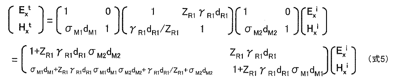
- an incident wave and a transmitted wave when a shield material is configured by a laminated structure of metal (M1) / resin (R1) / metal (M2) can be expressed by the following equations.
- the incident wave and the transmitted wave when the shield material is configured by a laminated structure of metal (M1) / resin (R1) / metal (M2) / resin (R2) / metal (M3) can be expressed by the following equations. it can.
- the shielding effect in the laminate of the metal foil and the insulating layer is obtained by increasing ⁇ M ⁇ d M ⁇ Z R ⁇ ⁇ R ⁇ d R for all combinations of the metal foil and the insulating layer to be used. It can be theoretically understood that it can be improved. However, as described in, for example, “Kenichi Hatakeyama,“ Electromagnetic shielding course for the first time ”Science Information Publishing (2013), p. 56”, conventionally (Z R ⁇ ⁇ R ⁇ d R ) is in the low frequency range. Therefore, according to this concept, ⁇ M ⁇ d M ⁇ Z R ⁇ ⁇ R ⁇ d R is also a parameter that can be approximated to 0.
- ⁇ M ⁇ d M ⁇ Z R ⁇ ⁇ R ⁇ d R becomes a large value that cannot be approximated to 0, and is low. It was found that there was a significant effect even in the frequency domain.
- the present inventor repeats the experiment of the shielding effect in the laminate of the metal foil and the insulating layer, and that ⁇ M ⁇ d M ⁇ d R has a significant influence even in a low frequency region of about 1 MHz.
- the shielding effect is that the metal foil and the insulating layer are selected so that all combinations of the metal foil and the insulating layer constituting the heading and the electromagnetic wave shielding material satisfy ⁇ M ⁇ d M ⁇ d R ⁇ 3 ⁇ 10 ⁇ 3.
- all combinations of the metal foil and the insulating layer constituting the electromagnetic wave shielding material satisfy ⁇ M ⁇ d M ⁇ d R ⁇ 1 ⁇ 10 ⁇ 2 , and ⁇ M ⁇ d M ⁇ d R ⁇ 4 ⁇ 10 ⁇ . 2 is more preferable, ⁇ M ⁇ d M ⁇ d R ⁇ 8 ⁇ 10 ⁇ 2 is still more preferable, and ⁇ M ⁇ d M ⁇ d R ⁇ 1 ⁇ 10 ⁇ 1 is even more preferable. preferable.
- ⁇ M ⁇ d M ⁇ d R No particular upper limit is set for ⁇ M ⁇ d M ⁇ d R , but usually ⁇ M ⁇ for all combinations of the metal foil and the insulating layer constituting the electromagnetic wave shielding material in consideration of the thickness and the material used.
- d M ⁇ d R ⁇ 10 typically ⁇ M ⁇ d M ⁇ d R ⁇ 1.
- an adhesive may be used between the insulating layer and the metal foil, or the insulating layer may be thermocompression bonded to the metal foil without using the adhesive. It is possible to simply overlap without using an adhesive, but considering the integrity of the electromagnetic shielding material, at least the edges (for example, each side when the shielding material is a square) should be joined with an adhesive or by thermocompression bonding. Is preferred. However, it is preferable to use an adhesive from the viewpoint of not applying excessive heat to the insulating layer.
- the adhesive is the same as described above, and there is no particular limitation, but acrylic resin, epoxy resin, urethane, polyester, silicone resin, vinyl acetate, styrene butadiene rubber, nitrile rubber, phenol Resin-based, cyanoacrylate-based and the like can be mentioned, and urethane-based, polyester-based, and vinyl acetate-based are preferable for ease of production and cost.
- the thickness of the adhesive layer is preferably 6 ⁇ m or less. When the thickness of the adhesive layer exceeds 6 ⁇ m, only the metal foil is easily broken after being laminated on the metal foil composite. However, when the adhesive layer as described above also serves as the insulating layer, the thickness is not limited to this, and the thickness described in the description of the insulating layer can be used.
- the electromagnetic wave shielding material according to the present invention needs to have a structure in which at least three metal foils are laminated via an insulating layer.
- the following is mentioned as an example of the laminated structure which comprises the said requirements.
- the layer indicated in parentheses may be added as appropriate.
- one “metal foil” can be formed by laminating a plurality of metal foils without using an insulating layer, and one “insulating layer” can also be used without using a metal foil.
- a plurality of insulating layers can be stacked.
- layers other than an insulating layer and metal foil can also be provided.
- the total thickness of the electromagnetic wave shielding material can be 50 to 1500 ⁇ m, can be 1000 ⁇ m or less, can be 600 ⁇ m or less, and can be 400 ⁇ m or less. It can also be 200 micrometers or less.
- the electromagnetic wave shielding material according to the present invention is particularly used for electric / electronic devices (for example, inverters, communication devices, resonators, electron tubes / discharge lamps, electric heating devices, electric motors, generators, electronic components, printed circuits, medical devices, etc.). Used for various electromagnetic shielding applications such as coating materials or exterior materials, harnesses and communication cable coating materials connected to electrical / electronic devices, electromagnetic shielding sheets, electromagnetic shielding panels, electromagnetic shielding bags, electromagnetic shielding boxes, electromagnetic shielding rooms, etc. It is possible.
- electric / electronic devices for example, inverters, communication devices, resonators, electron tubes / discharge lamps, electric heating devices, electric motors, generators, electronic components, printed circuits, medical devices, etc.
- electromagnetic shielding applications such as coating materials or exterior materials, harnesses and communication cable coating materials connected to electrical / electronic devices, electromagnetic shielding sheets, electromagnetic shielding panels, electromagnetic shielding bags, electromagnetic shielding boxes, electromagnetic shielding rooms, etc. It is possible.
- the electromagnetic wave shielding material it is possible to have a magnetic field shielding characteristic of 36 dB or more (how much the signal is attenuated on the receiving side) at 1 MHz, and preferably a magnetic field shielding characteristic of 40 dB or more. More preferably 50 dB or more, even more preferably 60 dB or more, even more preferably 70 dB or more. For example, it can have a magnetic field shielding characteristic of 36 to 90 dB.
- the magnetic field shield characteristic is measured by the KEC method.
- the KEC method refers to the “electromagnetic shielding characteristic measurement method” at the Kansai Electronics Industry Promotion Center.
- Comparative Example 3 Magnetic field shielding effect when three metal foils are laminated
- Comparative Example 1 was prepared by preparing three rolled copper foils (thickness: 33 ⁇ m), simply laminating them without using an adhesive, and installing them on a magnetic field shielding effect evaluation device (Techno Science Japan, Model TSES-KEC). The magnetic field shielding effect was evaluated by the same method.
- Comparative example 4 Magnetic shielding effect when two metal foils are laminated via an insulating layer
- PET polyethylene terephthalate
- a rolled copper foil with a thickness of 7 ⁇ m as a metal foil By using a polyethylene terephthalate (PET) film with a thickness of 250 ⁇ m as an insulating layer, a rolled copper foil with a thickness of 7 ⁇ m as a metal foil, and simply laminating without using an adhesive, the laminated structure shown in Table 1 is obtained. An electromagnetic shielding material was produced. This electromagnetic shielding material was installed in a magnetic field shielding effect evaluation apparatus (Techno Science Japan Model TSES-KEC), and the magnetic field shielding effect was evaluated in the same manner as in Comparative Example 1.
- a magnetic field shielding effect evaluation apparatus Techno Science Japan Model TSES-KEC
- Comparative Example 5 Magnetic field shielding effect when two metal foils are laminated via an insulating layer
- PET polyethylene terephthalate
- a rolled copper foil having a thickness of 8 ⁇ m as a metal foil By using a polyethylene terephthalate (PET) film having a thickness of 100 ⁇ m as an insulating layer, a rolled copper foil having a thickness of 8 ⁇ m as a metal foil, and simply laminating without using an adhesive, the laminated structure shown in Table 1 is obtained. An electromagnetic shielding material was produced. This electromagnetic shielding material was installed in a magnetic field shielding effect evaluation apparatus (Techno Science Japan Model TSES-KEC), and the magnetic field shielding effect was evaluated in the same manner as in Comparative Example 1.
- a magnetic field shielding effect evaluation apparatus Techno Science Japan Model TSES-KEC
- Comparative Example 6 Magnetic field shielding effect when two metal foils are installed via an air layer
- Air was used as the insulating layer, and aluminum foils having a thickness of 6 ⁇ m and 30 ⁇ m were used as the metal foils, and electromagnetic wave shielding materials having the laminated structure shown in Table 1 were produced.
- the two aluminum foils were arranged in parallel at an interval of 50 ⁇ m in the air with a copper plate having a large square opening at the center.
- This electromagnetic shielding material was installed in a magnetic field shielding effect evaluation apparatus (Techno Science Japan Model TSES-KEC), and the magnetic field shielding effect was evaluated in the same manner as in Comparative Example 1.
- Example 1 By using a polyimide (PI) film with a thickness of 100 ⁇ m as an insulating layer, a rolled copper foil with a thickness of 17 ⁇ m as a metal foil, and simply laminating without using an adhesive, an electromagnetic wave having the laminated structure shown in Table 1 A shield material was produced. This electromagnetic shielding material was installed in a magnetic field shielding effect evaluation apparatus (Techno Science Japan Model TSES-KEC), and the magnetic field shielding effect was evaluated in the same manner as in Comparative Example 1.
- PI polyimide
- Example 2 By using a polyethylene terephthalate (PET) film with a thickness of 100 ⁇ m as an insulating layer, an aluminum foil with a thickness of 20 ⁇ m as a metal foil, and simply laminating without using an adhesive, an electromagnetic wave having the laminated structure shown in Table 1 A shield material was produced. This electromagnetic shielding material was installed in a magnetic field shielding effect evaluation apparatus (Techno Science Japan Model TSES-KEC), and the magnetic field shielding effect was evaluated in the same manner as in Comparative Example 1.
- PET polyethylene terephthalate
- Example 3 By using a polyethylene terephthalate (PET) film having a thickness of 100 ⁇ m as an insulating layer, an electrolytic copper foil having a thickness of 30 ⁇ m as a metal foil, and simply laminating without using an adhesive, the laminated structure shown in Table 1 is obtained. An electromagnetic shielding material was produced. This electromagnetic shielding material was installed in a magnetic field shielding effect evaluation apparatus (Techno Science Japan Model TSES-KEC), and the magnetic field shielding effect was evaluated in the same manner as in Comparative Example 1.
- a magnetic field shielding effect evaluation apparatus Techno Science Japan Model TSES-KEC
- Example 4 By using a polyethylene terephthalate (PET) film having a thickness of 100 ⁇ m as an insulating layer, a nickel foil having a thickness of 50 ⁇ m as a metal foil, and simply laminating without using an adhesive, electromagnetic waves having the laminated structure shown in Table 1 A shield material was produced. This electromagnetic shielding material was installed in a magnetic field shielding effect evaluation apparatus (Techno Science Japan Model TSES-KEC), and the magnetic field shielding effect was evaluated in the same manner as in Comparative Example 1.
- PET polyethylene terephthalate
- a nickel foil having a thickness of 50 ⁇ m as a metal foil
- Example 5 By using a polyethylene terephthalate (PET) film having a thickness of 100 ⁇ m as an insulating layer, a soft iron foil having a thickness of 50 ⁇ m as a metal foil, and simply laminating without using an adhesive, an electromagnetic wave having a laminated structure described in Table 1 A shield material was produced. This electromagnetic shielding material was installed in a magnetic field shielding effect evaluation apparatus (Techno Science Japan Model TSES-KEC), and the magnetic field shielding effect was evaluated in the same manner as in Comparative Example 1.
- PET polyethylene terephthalate
- Example 6 By using a polytetrafluoroethylene (PTFE) film having a thickness of 500 ⁇ m as an insulating layer, a stainless steel foil having a thickness of 50 ⁇ m as a metal foil, and simply laminating without using an adhesive, the laminated structure shown in Table 1 is obtained. An electromagnetic wave shielding material having the same was produced. This electromagnetic shielding material was installed in a magnetic field shielding effect evaluation apparatus (Techno Science Japan Model TSES-KEC), and the magnetic field shielding effect was evaluated in the same manner as in Comparative Example 1.
- PTFE polytetrafluoroethylene
- Example 7 By using a polyethylene terephthalate (PET) film having a thickness of 100 ⁇ m as an insulating layer, a rolled copper foil having a thickness of 6 ⁇ m as a metal foil, and simply laminating without using an adhesive, the laminated structure shown in Table 1 is obtained. An electromagnetic shielding material was produced. This electromagnetic shielding material was installed in a magnetic field shielding effect evaluation apparatus (Techno Science Japan Model TSES-KEC), and the magnetic field shielding effect was evaluated in the same manner as in Comparative Example 1.
- a magnetic field shielding effect evaluation apparatus Techno Science Japan Model TSES-KEC
- Example 8 By using a polyethylene terephthalate (PET) film having a thickness of 100 ⁇ m as an insulating layer, a rolled copper foil having a thickness of 17 ⁇ m as a metal foil, and simply laminating without using an adhesive, the laminated structure shown in Table 1 is obtained. An electromagnetic shielding material was produced. This electromagnetic shielding material was installed in a magnetic field shielding effect evaluation apparatus (Techno Science Japan Model TSES-KEC), and the magnetic field shielding effect was evaluated in the same manner as in Comparative Example 1.
- a magnetic field shielding effect evaluation apparatus Techno Science Japan Model TSES-KEC
- Example 9 By using a polyethylene terephthalate (PET) film having a thickness of 100 ⁇ m as an insulating layer, a rolled copper foil having a thickness of 33 ⁇ m as a metal foil, and simply laminating without using an adhesive, the laminated structure shown in Table 1 is obtained. An electromagnetic shielding material was produced. This electromagnetic shielding material was installed in a magnetic field shielding effect evaluation apparatus (Techno Science Japan Model TSES-KEC), and the magnetic field shielding effect was evaluated in the same manner as in Comparative Example 1.
- PET polyethylene terephthalate
- Example 10 By using a polyethylene terephthalate (PET) film with a thickness of 9 ⁇ m as an insulating layer, a rolled copper foil with a thickness of 7 ⁇ m and 33 ⁇ m as a metal foil, and simply laminating without using an adhesive, the laminated structure described in Table 1 An electromagnetic shielding material having a thickness of 10 was prepared. This electromagnetic shielding material was installed in a magnetic field shielding effect evaluation apparatus (Techno Science Japan Model TSES-KEC), and the magnetic field shielding effect was evaluated in the same manner as in Comparative Example 1.
- a magnetic field shielding effect evaluation apparatus Techno Science Japan Model TSES-KEC
- Example 11 By using a polyethylene terephthalate (PET) film having a thickness of 500 ⁇ m as an insulating layer, a rolled copper foil having a thickness of 17 ⁇ m as a metal foil, and simply laminating without using an adhesive, the laminated structure shown in Table 1 is obtained. An electromagnetic shielding material was produced. This electromagnetic shielding material was installed in a magnetic field shielding effect evaluation apparatus (Techno Science Japan Model TSES-KEC), and the magnetic field shielding effect was evaluated in the same manner as in Comparative Example 1.
- PET polyethylene terephthalate
- Example 12 By using a polytetrafluoroethylene (PTFE) film having a thickness of 100 ⁇ m as an insulating layer, a rolled copper foil having a thickness of 17 ⁇ m as a metal foil, and simply laminating without using an adhesive, the laminated structure shown in Table 1 An electromagnetic shielding material having a thickness of 10 was prepared. This electromagnetic shielding material was installed in a magnetic field shielding effect evaluation apparatus (Techno Science Japan Model TSES-KEC), and the magnetic field shielding effect was evaluated in the same manner as in Comparative Example 1.
- PTFE polytetrafluoroethylene
- Example 13 An electromagnetic wave having a laminated structure shown in Table 1 by using a polyamide (PA) film having a thickness of 100 ⁇ m as an insulating layer, a rolled copper foil having a thickness of 17 ⁇ m as a metal foil, and simply laminating without using an adhesive. A shield material was produced. This electromagnetic shielding material was installed in a magnetic field shielding effect evaluation apparatus (Techno Science Japan Model TSES-KEC), and the magnetic field shielding effect was evaluated in the same manner as in Comparative Example 1.
- PA polyamide
- TSES-KEC Magnetic field shielding effect evaluation apparatus
- Example 14 By using a polyethylene terephthalate (PET) film having a thickness of 100 ⁇ m as the insulating layer, a rolled copper foil having a thickness of 33 ⁇ m and a nickel foil having a thickness of 30 ⁇ m as the metal foil, and simply laminating without using an adhesive, Table 1 An electromagnetic shielding material having the described laminated structure was produced. This electromagnetic shielding material was installed in a magnetic field shielding effect evaluation apparatus (Techno Science Japan Model TSES-KEC), and the magnetic field shielding effect was evaluated in the same manner as in Comparative Example 1.
- a magnetic field shielding effect evaluation apparatus Techno Science Japan Model TSES-KEC
- Example 15 By using a polyethylene terephthalate (PET) film having a thickness of 12 ⁇ m as the insulating layer, a rolled copper foil having a thickness of 12 ⁇ m and a rolled copper foil having a thickness of 17 ⁇ m as the metal foil, and simply laminating without using an adhesive, Table 1 An electromagnetic shielding material having the laminated structure described in 1 was produced. This electromagnetic shielding material was installed in a magnetic field shielding effect evaluation apparatus (Techno Science Japan Model TSES-KEC), and the magnetic field shielding effect was evaluated in the same manner as in Comparative Example 1.
- a magnetic field shielding effect evaluation apparatus Techno Science Japan Model TSES-KEC
- Example 16 By using a polyethylene terephthalate (PET) film having a thickness of 100 ⁇ m as an insulating layer, a rolled copper foil having a thickness of 12 ⁇ m as a metal foil, and simply laminating without using an adhesive, the laminated structure shown in Table 1 is obtained. An electromagnetic shielding material was produced. This electromagnetic shielding material was installed in a magnetic field shielding effect evaluation apparatus (Techno Science Japan Model TSES-KEC), and the magnetic field shielding effect was evaluated in the same manner as in Comparative Example 1.
- PET polyethylene terephthalate
- Example 17 By using a polyethylene terephthalate (PET) film with a thickness of 9 ⁇ m as an insulating layer, an aluminum foil with a thickness of 20 ⁇ m as a metal foil, and simply laminating without using an adhesive, an electromagnetic wave having the laminated structure shown in Table 1 A shield material was produced. This electromagnetic shielding material was installed in a magnetic field shielding effect evaluation apparatus (Techno Science Japan Model TSES-KEC), and the magnetic field shielding effect was evaluated in the same manner as in Comparative Example 1.
- PET polyethylene terephthalate
- Example 1 in which three metal foils are laminated via an insulating layer, and ⁇ M ⁇ d M ⁇ d R is 3 ⁇ 10 ⁇ 3 or more for all combinations of the metal foil and the insulating layer. It can be understood that the shielding effect is remarkably excellent. For example, in contrast to Comparative Example 1 in which a thickness of 150 ⁇ m was required to obtain a shielding effect of 31.1 dB with a single copper foil, Example 1 uses only a copper foil having a thickness of about 1/3. Nevertheless, the shielding effect is improved by about 26 dB.
- Example 2 uses only an aluminum foil having a thickness of 1/5. Nevertheless, the shielding effect is improved by about 19 dB.
- the minimum sigma M d M d prefer R is higher in the combination of the metal foil and the insulating layer, it can understand that a high shielding effect while reducing the total thickness of the metal foil can be obtained.
- the total thickness of the copper foil is 51 ⁇ m, but it can be seen that there is a large difference in the shielding effect due to the difference in the minimum ⁇ M d M d R.
Landscapes
- Chemical & Material Sciences (AREA)
- Engineering & Computer Science (AREA)
- Microelectronics & Electronic Packaging (AREA)
- Chemical Kinetics & Catalysis (AREA)
- Materials Engineering (AREA)
- Mechanical Engineering (AREA)
- Metallurgy (AREA)
- Organic Chemistry (AREA)
- Physics & Mathematics (AREA)
- Electromagnetism (AREA)
- Shielding Devices Or Components To Electric Or Magnetic Fields (AREA)
- Laminated Bodies (AREA)
Abstract
Description
少なくとも3枚の金属箔が絶縁層を介して積層された構造を有する電磁波シールド材であって、当該電磁波シールド材を構成する金属箔と絶縁層のすべての組み合わせが、σM×dM×dR≧3×10⁻³を満たす電磁波シールド材。
但し、式中の記号は以下を示す。
σM:金属箔の20℃における導電率(S/m)
dM:金属箔の厚み(m)
dR:絶縁層の厚み(m)
本発明に係る電磁波シールド材に使用する金属箔の材料としては特に制限はないが、交流磁界や交流電界に対するシールド特性を高める観点からは、導電性に優れた金属材料とすることが好ましい。具体的には、導電率が1.0×10⁶S/m(20℃の値。以下同じ。)以上の金属によって形成することが好ましく、金属の導電率が10.0×106S/m以上であるとより好ましく、30.0×106S/m以上であると更により好ましく、50.0×106S/m以上であると最も好ましい。このような金属としては、導電率が約9.9×106S/mの鉄、導電率が約14.5×106S/mのニッケル、導電率が約39.6×106S/mのアルミニウム、導電率が約58.0×106S/mの銅、及び導電率が約61.4×106S/mの銀が挙げられる。電気抵抗率とコストの双方を考慮すると、アルミニウム又は銅を採用することが実用性上好ましい。本発明に係る電磁波シールド材中に使用する金属箔はすべて同一の金属であってもよいし、層毎に異なる金属を使用してもよい。また、上述した金属の合金を使用することもできる。金属箔表面には接着促進、耐環境性、耐熱及び防錆などを目的とした各種の表面処理層が形成されていてもよい。
本発明に係る電磁波シールド材において、複数枚の金属箔を積層することによる電磁波シールド効果の顕著な改善は、金属箔と金属箔の間に絶縁層を挟み込むことで得られる。金属箔同士を直接重ねても、金属箔の合計厚みが増えることでシールド効果が向上するものの、顕著な向上効果は得られない。これは、金属箔間に絶縁層が存在することで電磁波の反射回数が増えて、電磁波が減衰されることによると考えられる。
本明細書で使用する各種記号は以下のように定義される。
σM:金属箔の20℃における導電率(S/m)
dM:金属箔の厚み(m)
ZR:絶縁層のインピーダンス(Ω)=Z0×√(1/εR)
εR:絶縁層の20℃における比誘電率
γR:伝搬定数=j×2π√(εR/λ);jは虚数単位
λ:波長(m):1MHzでは300m
dR:絶縁層の厚み(m)
Zo:真空のインピーダンス=377Ω
本発明に係る電磁波シールド材は、上述した金属箔と絶縁層を積層することで製造可能である。この際、電磁波シールド材を構成する金属箔と絶縁層のすべての組み合わせが、σM×dM×dR≧3×10⁻³を満たすように、金属箔と絶縁層を選択することが、電磁波シールド効果を顕著に高める観点から重要となる。






A=1+ZR1γR1dR1σM2dM2+ZR2γR2dR2σM3dM3+ZR1γR1dR1σM3dM3+ZR1γR1dR1ZR2γR2dR2σM2dM2σM3dM3
B=ZR2γR2dR2+ZR1γR1dR1ZR2γR2dR2σM2dM2+ZR1γR1dR1
C=σM1dM1+σM2dM2+σM3dM3+γR1dR1/ZR1+γR2dR2/ZR2+ZR1γR1dR1σM1dM1+ZR1γR1dR1σM1dM1σM3dM3+ZR1γR1dR1ZR2γR2dR2σM1dM1σM2dM2σM3dM3+ZR2γR2dR2σM2dM2σM3dM3+ZR2γR2dR2σM3dM3γR1dR1/ZR1
D=ZR2γR2dR2σM1dM1+ZR2γR2dR2σM1dM1σM2dM2+ZR2γR2dR2σM2dM2+ZR1γR1dR1σM1dM1+ZR2γR2dR2γR1dR1/ZR1
(1)(絶縁層)/金属箔/絶縁層/金属箔/絶縁層/金属層/(絶縁層)
(2)(絶縁層)/金属箔/絶縁層/金属箔/絶縁層/金属箔/絶縁層/金属箔/(絶縁層)
(1)及び(2)においては、一つの「金属箔」は絶縁層を介することなく複数の金属箔を積層して構成することができ、一つの「絶縁層」も金属箔を介することなく複数の絶縁層を積層して構成することができる。また、絶縁層や金属箔以外の層を設けることもできる。
Cu:圧延銅箔(20℃での導電率:58.0×10⁶S/m)
Al:アルミ箔(20℃での導電率:39.6×10⁶S/m)
電解Cu:電解銅箔(20℃での導電率:56.0×10⁶S/m)
Ni:ニッケル箔(20℃での導電率:14.5×10⁶S/m)
Fe:軟鉄箔(20℃での導電率:9.9×10⁶S/m)
sus:ステンレス箔(20℃での導電率:1.4×10⁶S/m)
PI:ポリイミドフィルム(20℃での比誘電率:3.5)
PET:ポリエチレンテレフタレートフィルム(20℃での比誘電率:3.0)
PTFE:ポリテトラフルオロエチレンフィルム(20℃での比誘電率:2.1)
PA:ポリアミドフィルム(20℃での比誘電率:6.0)
空隙:金属箔同士を空気で隔てた(20℃での比誘電率:1.0)
圧延銅箔(厚み:150μm)及びアルミ箔(厚み:300μm)について、単層での磁界シールド効果を調査した。用意した金属材料を磁界シールド効果評価装置(テクノサイエンスジャパン社 型式TSES-KEC)に設置して、周波数を1MHzとし、20℃の条件下で、KEC法により磁界シールド効果を評価した。
圧延銅箔(厚み:33μm)を3枚用意し、これを接着剤を介することなく単純に積層し、磁界シールド効果評価装置(テクノサイエンスジャパン社 型式TSES-KEC)に設置して、比較例1と同様の方法で磁界シールド効果を評価した。
絶縁層として厚さ250μmのポリエチレンテレフタレート(PET)フィルムを用い、金属箔として厚み7μmの圧延銅箔を用い、接着剤を使用せずに単に積層することで、表1に記載の積層構造をもつ電磁波シールド材を作製した。この電磁波シールド材を磁界シールド効果評価装置(テクノサイエンスジャパン社 型式TSES-KEC)に設置して、比較例1と同様の方法で磁界シールド効果を評価した。
絶縁層として厚さ100μmのポリエチレンテレフタレート(PET)フィルムを用い、金属箔として厚み8μmの圧延銅箔を用い、接着剤を使用せずに単に積層することで、表1に記載の積層構造をもつ電磁波シールド材を作製した。この電磁波シールド材を磁界シールド効果評価装置(テクノサイエンスジャパン社 型式TSES-KEC)に設置して、比較例1と同様の方法で磁界シールド効果を評価した。
絶縁層として空気を用い、金属箔として厚み6μm及び30μmのアルミ箔を用い、表1に記載の積層構造をもつ電磁波シールド材を作製した。この例において、2枚のアルミ箔は中央部に正方形状の大きな開口部を有する銅板を挟んで空気中で50μmの間隔で平行に配置した。この電磁波シールド材を磁界シールド効果評価装置(テクノサイエンスジャパン社 型式TSES-KEC)に設置して、比較例1と同様の方法で磁界シールド効果を評価した。
絶縁層として厚さ9μmのポリイミド(PI)フィルムを用い、金属箔として厚み6μmのアルミ箔を用い、接着剤を使用せずに単に積層することで、表1に記載の積層構造をもつ電磁波シールド材を作製した。この電磁波シールド材を磁界シールド効果評価装置(テクノサイエンスジャパン社 型式TSES-KEC)に設置して、比較例1と同様の方法で磁界シールド効果を評価した。
絶縁層として厚さ100μmのポリイミド(PI)フィルムを用い、金属箔として厚み17μmの圧延銅箔を用い、接着剤を使用せずに単に積層することで、表1に記載の積層構造をもつ電磁波シールド材を作製した。この電磁波シールド材を磁界シールド効果評価装置(テクノサイエンスジャパン社 型式TSES-KEC)に設置して、比較例1と同様の方法で磁界シールド効果を評価した。
絶縁層として厚さ100μmのポリエチレンテレフタレート(PET)フィルムを用い、金属箔として厚み20μmのアルミ箔を用い、接着剤を使用せずに単に積層することで、表1に記載の積層構造をもつ電磁波シールド材を作製した。この電磁波シールド材を磁界シールド効果評価装置(テクノサイエンスジャパン社 型式TSES-KEC)に設置して、比較例1と同様の方法で磁界シールド効果を評価した。
絶縁層として厚さ100μmのポリエチレンテレフタレート(PET)フィルムを用い、金属箔として厚み30μmの電解銅箔を用い、接着剤を使用せずに単に積層することで、表1に記載の積層構造をもつ電磁波シールド材を作製した。この電磁波シールド材を磁界シールド効果評価装置(テクノサイエンスジャパン社 型式TSES-KEC)に設置して、比較例1と同様の方法で磁界シールド効果を評価した。
絶縁層として厚さ100μmのポリエチレンテレフタレート(PET)フィルムを用い、金属箔として厚み50μmのニッケル箔を用い、接着剤を使用せずに単に積層することで、表1に記載の積層構造をもつ電磁波シールド材を作製した。この電磁波シールド材を磁界シールド効果評価装置(テクノサイエンスジャパン社 型式TSES-KEC)に設置して、比較例1と同様の方法で磁界シールド効果を評価した。
絶縁層として厚さ100μmのポリエチレンテレフタレート(PET)フィルムを用い、金属箔として厚み50μmの軟鉄箔を用い、接着剤を使用せずに単に積層することで、表1に記載の積層構造をもつ電磁波シールド材を作製した。この電磁波シールド材を磁界シールド効果評価装置(テクノサイエンスジャパン社 型式TSES-KEC)に設置して、比較例1と同様の方法で磁界シールド効果を評価した。
絶縁層として厚さ500μmのポリテトラフルオロエチレン(PTFE)フィルムを用い、金属箔として厚み50μmのステンレス箔を用い、接着剤を使用せずに単に積層することで、表1に記載の積層構造をもつ電磁波シールド材を作製した。この電磁波シールド材を磁界シールド効果評価装置(テクノサイエンスジャパン社 型式TSES-KEC)に設置して、比較例1と同様の方法で磁界シールド効果を評価した。
絶縁層として厚さ100μmのポリエチレンテレフタレート(PET)フィルムを用い、金属箔として厚み6μmの圧延銅箔を用い、接着剤を使用せずに単に積層することで、表1に記載の積層構造をもつ電磁波シールド材を作製した。この電磁波シールド材を磁界シールド効果評価装置(テクノサイエンスジャパン社 型式TSES-KEC)に設置して、比較例1と同様の方法で磁界シールド効果を評価した。
絶縁層として厚さ100μmのポリエチレンテレフタレート(PET)フィルムを用い、金属箔として厚み17μmの圧延銅箔を用い、接着剤を使用せずに単に積層することで、表1に記載の積層構造をもつ電磁波シールド材を作製した。この電磁波シールド材を磁界シールド効果評価装置(テクノサイエンスジャパン社 型式TSES-KEC)に設置して、比較例1と同様の方法で磁界シールド効果を評価した。
絶縁層として厚さ100μmのポリエチレンテレフタレート(PET)フィルムを用い、金属箔として厚み33μmの圧延銅箔を用い、接着剤を使用せずに単に積層することで、表1に記載の積層構造をもつ電磁波シールド材を作製した。この電磁波シールド材を磁界シールド効果評価装置(テクノサイエンスジャパン社 型式TSES-KEC)に設置して、比較例1と同様の方法で磁界シールド効果を評価した。
絶縁層として厚さ9μmのポリエチレンテレフタレート(PET)フィルムを用い、金属箔として厚み7μm及び33μmの圧延銅箔を用い、接着剤を使用せずに単に積層することで、表1に記載の積層構造をもつ電磁波シールド材を作製した。この電磁波シールド材を磁界シールド効果評価装置(テクノサイエンスジャパン社 型式TSES-KEC)に設置して、比較例1と同様の方法で磁界シールド効果を評価した。
絶縁層として厚さ500μmのポリエチレンテレフタレート(PET)フィルムを用い、金属箔として厚み17μmの圧延銅箔を用い、接着剤を使用せずに単に積層することで、表1に記載の積層構造をもつ電磁波シールド材を作製した。この電磁波シールド材を磁界シールド効果評価装置(テクノサイエンスジャパン社 型式TSES-KEC)に設置して、比較例1と同様の方法で磁界シールド効果を評価した。
絶縁層として厚さ100μmのポリテトラフルオロエチレン(PTFE)フィルムを用い、金属箔として厚み17μmの圧延銅箔を用い、接着剤を使用せずに単に積層することで、表1に記載の積層構造をもつ電磁波シールド材を作製した。この電磁波シールド材を磁界シールド効果評価装置(テクノサイエンスジャパン社 型式TSES-KEC)に設置して、比較例1と同様の方法で磁界シールド効果を評価した。
絶縁層として厚さ100μmのポリアミド(PA)フィルムを用い、金属箔として厚み17μmの圧延銅箔を用い、接着剤を使用せずに単に積層することで、表1に記載の積層構造をもつ電磁波シールド材を作製した。この電磁波シールド材を磁界シールド効果評価装置(テクノサイエンスジャパン社 型式TSES-KEC)に設置して、比較例1と同様の方法で磁界シールド効果を評価した。
絶縁層として厚さ100μmのポリエチレンテレフタレート(PET)フィルムを用い、金属箔として厚み33μmの圧延銅箔と厚み30μmのニッケル箔を用い、接着剤を使用せずに単に積層することで、表1に記載の積層構造をもつ電磁波シールド材を作製した。この電磁波シールド材を磁界シールド効果評価装置(テクノサイエンスジャパン社 型式TSES-KEC)に設置して、比較例1と同様の方法で磁界シールド効果を評価した。
絶縁層として厚さ12μmのポリエチレンテレフタレート(PET)フィルムを用い、金属箔として厚み12μmの圧延銅箔と厚み17μmの圧延銅箔を用い、接着剤を使用せずに単に積層することで、表1に記載の積層構造をもつ電磁波シールド材を作製した。この電磁波シールド材を磁界シールド効果評価装置(テクノサイエンスジャパン社 型式TSES-KEC)に設置して、比較例1と同様の方法で磁界シールド効果を評価した。
絶縁層として厚さ100μmのポリエチレンテレフタレート(PET)フィルムを用い、金属箔として厚み12μmの圧延銅箔を用い、接着剤を使用せずに単に積層することで、表1に記載の積層構造をもつ電磁波シールド材を作製した。この電磁波シールド材を磁界シールド効果評価装置(テクノサイエンスジャパン社 型式TSES-KEC)に設置して、比較例1と同様の方法で磁界シールド効果を評価した。
絶縁層として厚さ9μmのポリエチレンテレフタレート(PET)フィルムを用い、金属箔として厚み20μmのアルミ箔を用い、接着剤を使用せずに単に積層することで、表1に記載の積層構造をもつ電磁波シールド材を作製した。この電磁波シールド材を磁界シールド効果評価装置(テクノサイエンスジャパン社 型式TSES-KEC)に設置して、比較例1と同様の方法で磁界シールド効果を評価した。

Claims (8)
- 少なくとも3枚の金属箔が絶縁層を介して積層された構造を有する電磁波シールド材であって、当該電磁波シールド材を構成する金属箔と絶縁層のすべての組み合わせが、σM×dM×dR≧3×10⁻³を満たす電磁波シールド材。
但し、式中の記号は以下を示す。
σM:金属箔の20℃における導電率(S/m)
dM:金属箔の厚み(m)
dR:絶縁層の厚み(m) - 各金属箔の20℃における導電率が1.0×10⁶S/m以上である請求項1に記載の電磁波シールド材。
- 各金属箔の厚みが4~100μmである請求項1又は2に記載の電磁波シールド材。
- 各絶縁層の20℃における比誘電率が2.0~10.0である請求項1~3の何れか一項に記載の電磁波シールド材。
- 各絶縁層の厚みが4~500μmである請求項1~4の何れか一項に記載の電磁波シールド材。
- 金属箔の合計厚みが15~150μmである請求項1~5の何れか一項に記載の電磁波シールド材。
- 請求項1~6の何れか一項に記載の電磁波シールド材を備えた電気・電子機器用の被覆材又は外装材。
- 請求項7に記載の被覆材又は外装材を備えた電気・電子機器。
Priority Applications (5)
| Application Number | Priority Date | Filing Date | Title |
|---|---|---|---|
| KR1020197006346A KR102245327B1 (ko) | 2015-03-30 | 2015-06-18 | 전자파 실드재 |
| US15/562,472 US10442159B2 (en) | 2015-03-30 | 2015-06-18 | Electromagnetic shielding material |
| CN201580078485.9A CN107409482B (zh) | 2015-03-30 | 2015-06-18 | 电磁波屏蔽材料 |
| KR1020177026932A KR20170127474A (ko) | 2015-03-30 | 2015-06-18 | 전자파 실드재 |
| EP15887696.1A EP3280236B1 (en) | 2015-03-30 | 2015-06-18 | Electromagnetic shielding material |
Applications Claiming Priority (2)
| Application Number | Priority Date | Filing Date | Title |
|---|---|---|---|
| JP2015070091A JP6278922B2 (ja) | 2015-03-30 | 2015-03-30 | 電磁波シールド材 |
| JP2015-070091 | 2015-03-30 |
Publications (1)
| Publication Number | Publication Date |
|---|---|
| WO2016157554A1 true WO2016157554A1 (ja) | 2016-10-06 |
Family
ID=57004869
Family Applications (1)
| Application Number | Title | Priority Date | Filing Date |
|---|---|---|---|
| PCT/JP2015/067662 Ceased WO2016157554A1 (ja) | 2015-03-30 | 2015-06-18 | 電磁波シールド材 |
Country Status (7)
| Country | Link |
|---|---|
| US (1) | US10442159B2 (ja) |
| EP (1) | EP3280236B1 (ja) |
| JP (1) | JP6278922B2 (ja) |
| KR (2) | KR102245327B1 (ja) |
| CN (1) | CN107409482B (ja) |
| TW (2) | TW201945184A (ja) |
| WO (1) | WO2016157554A1 (ja) |
Families Citing this family (10)
| Publication number | Priority date | Publication date | Assignee | Title |
|---|---|---|---|---|
| JP6379071B2 (ja) * | 2015-06-15 | 2018-08-22 | Jx金属株式会社 | 電磁波シールド材 |
| JP6341948B2 (ja) * | 2016-03-31 | 2018-06-13 | Jx金属株式会社 | 電磁波シールド材 |
| JP6883449B2 (ja) * | 2017-03-13 | 2021-06-09 | Jx金属株式会社 | 電磁波シールド材 |
| KR102274518B1 (ko) | 2017-09-29 | 2021-07-06 | 주식회사 엘지에너지솔루션 | 전지 셀 표면 냉각을 위한 불균일 유로를 구비한 쿨링 자켓 및 이를 포함하는 배터리 모듈 |
| CN115559148A (zh) * | 2018-09-19 | 2023-01-03 | 三菱制纸株式会社 | 电磁波屏蔽材料用无纺布及电磁波屏蔽材料 |
| WO2021199477A1 (ja) * | 2020-03-30 | 2021-10-07 | タツタ電線株式会社 | 電磁波シールド材料およびその製造方法 |
| JP7008121B1 (ja) | 2020-12-09 | 2022-01-25 | Jx金属株式会社 | 電磁波シールド材 |
| JP2022153032A (ja) | 2021-03-29 | 2022-10-12 | Jx金属株式会社 | 積層体及びその製造方法 |
| CN115401960A (zh) * | 2022-09-01 | 2022-11-29 | 哈尔滨玻璃钢研究院有限公司 | 一种高电磁屏蔽效能树脂基复合材料及其成型方法和应用 |
| US20260075786A1 (en) * | 2022-11-08 | 2026-03-12 | Jx Advanced Metals Corporation | Electromagnetic Wave Shielding Material, Covering Material or Exterior Material, and Electric/Electronic Apparatus |
Citations (5)
| Publication number | Priority date | Publication date | Assignee | Title |
|---|---|---|---|---|
| JP2003060387A (ja) * | 2001-08-17 | 2003-02-28 | Furukawa Techno Research Kk | 電磁波シールド材 |
| JP2006135020A (ja) * | 2004-11-04 | 2006-05-25 | Kitagawa Ind Co Ltd | 電磁波シールドフィルム |
| JP2006156946A (ja) * | 2004-11-04 | 2006-06-15 | Kitagawa Ind Co Ltd | 電磁波シールドフィルム |
| JP2010168605A (ja) * | 2009-01-20 | 2010-08-05 | Nippon Mining & Metals Co Ltd | 水濡れ性に優れた銅箔及びその製造方法 |
| WO2011121801A1 (ja) * | 2010-03-30 | 2011-10-06 | Jx日鉱日石金属株式会社 | 電磁波シールド用複合体 |
Family Cites Families (38)
| Publication number | Priority date | Publication date | Assignee | Title |
|---|---|---|---|---|
| JPS462680Y1 (ja) | 1968-11-05 | 1971-01-29 | ||
| US4507359A (en) * | 1980-12-22 | 1985-03-26 | Chomerics, Inc. | Electromagnetic shielding |
| US4412255A (en) * | 1981-02-23 | 1983-10-25 | Optical Coating Laboratory, Inc. | Transparent electromagnetic shield and method of manufacturing |
| DE3430406A1 (de) * | 1983-08-20 | 1985-03-14 | Riken EMC Co., Ltd., Nagoya, Aichi | Transparente platte fuer optische zeichenwiedergabevorrichtung |
| JPS60125125U (ja) * | 1984-02-03 | 1985-08-23 | 藤森工業株式会社 | 電磁波シ−ルド用積層材 |
| DE3777172D1 (de) * | 1987-05-20 | 1992-04-09 | Shimizu Construction Co Ltd | Elektromagnetische schirmstruktur fuer fenster von gebaeuden. |
| EP0322720A3 (en) * | 1987-12-25 | 1990-01-17 | Asahi Glass Company Ltd. | Electromagnetic wave shielding transparent body |
| US4965408A (en) | 1989-02-01 | 1990-10-23 | Borden, Inc. | Composite sheet material for electromagnetic radiation shielding |
| GB8918859D0 (en) * | 1989-08-18 | 1989-09-27 | Pilkington Plc | Electromagnetic shielding panel |
| US5260128A (en) * | 1989-12-11 | 1993-11-09 | Kabushiki Kaisha Riken | Electromagnetic shielding sheet |
| JPH03280500A (ja) * | 1990-03-28 | 1991-12-11 | Fujita Corp | 電磁波シールド内装材 |
| US5401901A (en) * | 1991-09-19 | 1995-03-28 | W. L. Gore & Associates, Inc. | Weather-resistant electromagnetic interference shielding for electronic equipment enclosures |
| DE69211009T2 (de) * | 1991-10-23 | 1996-11-28 | Gore & Ass | Abschirmungsfilter gegen elektromagnetische interferenz |
| JPH07290449A (ja) | 1994-04-27 | 1995-11-07 | Matsushita Electric Works Ltd | シート状の電磁波シールド成形材料及びその製造方法 |
| JP3017484B1 (ja) * | 1998-11-30 | 2000-03-06 | 東日電線株式会社 | 磁性箔とプラスチックの積層テープ及びそれを用いた電線 |
| JP2001283664A (ja) * | 2000-03-30 | 2001-10-12 | Kazuo Okabe | 柔軟な絶縁シールドカバー材 |
| US20040219328A1 (en) * | 2001-08-31 | 2004-11-04 | Kazunori Tasaki | Laminated soft magnetic member, soft magnetic sheet and production method for laminated soft magnetic member |
| JP4235396B2 (ja) | 2002-03-29 | 2009-03-11 | 真和工業株式会社 | インバータカバー |
| KR20050029312A (ko) * | 2002-08-08 | 2005-03-25 | 다이니폰 인사츠 가부시키가이샤 | 전자파 차폐용 시트 |
| FR2854940B1 (fr) | 2003-05-16 | 2005-07-15 | A T I | Isolant multicouche |
| JP4602680B2 (ja) | 2004-03-22 | 2010-12-22 | 株式会社オーツカ | 電磁波シールド構造 |
| US7113410B2 (en) * | 2004-04-01 | 2006-09-26 | Lucent Technologies, Inc. | Electromagnetic shield assembly with opposed hook flanges |
| US8134084B2 (en) | 2006-06-30 | 2012-03-13 | Shin-Etsu Polymer Co., Ltd. | Noise-suppressing wiring-member and printed wiring board |
| KR100962924B1 (ko) | 2006-07-14 | 2010-06-10 | 삼성코닝정밀소재 주식회사 | 전자파 차폐용 광학 부재, 이를 포함하는 광학 필터 및디스플레이 장치 |
| JPWO2008029776A1 (ja) | 2006-09-04 | 2010-01-21 | 東レ株式会社 | 光透過性電磁波シールド部材およびその製造方法 |
| WO2008126690A1 (ja) * | 2007-03-29 | 2008-10-23 | Kabushiki Kaisha Asahi Rubber | 電磁波シールドシート及びrfidプレート |
| US20100214713A1 (en) * | 2007-04-24 | 2010-08-26 | Nano Interface Technology | Laminate sheet for electromagnetic radiation shielding and grounding |
| WO2010064630A1 (ja) * | 2008-12-02 | 2010-06-10 | 大日本印刷株式会社 | 電磁波シールド材、及びその製造方法 |
| JP5268748B2 (ja) * | 2009-03-31 | 2013-08-21 | Jx日鉱日石金属株式会社 | Sn又はSn合金めっき被膜、及びそれを有する複合材料 |
| EP2416639B1 (en) | 2009-03-31 | 2018-11-28 | JX Nippon Mining & Metals Corporation | Electromagnetic shielding material and process for producing electromagnetic shielding material |
| JP5722775B2 (ja) * | 2009-07-24 | 2015-05-27 | 旭化成せんい株式会社 | 電磁波シールドシート |
| US20140113121A1 (en) * | 2011-03-31 | 2014-04-24 | Jx Nippon Mining & Metals Corporation | Metal foil composite, flexible printed circuit, formed product and method of producing the same |
| DE102011056807A1 (de) * | 2011-12-21 | 2013-06-27 | Thyssenkrupp Electrical Steel Gmbh | Magnetfeldabschirmung für elektromagnetische Felder und Fahrzeug mit integrierter Magnetfeldabschirmung |
| JP2013145778A (ja) * | 2012-01-13 | 2013-07-25 | Zippertubing (Japan) Ltd | 積層体及び電磁波シールドカバー |
| JP6061177B2 (ja) * | 2012-05-14 | 2017-01-18 | 株式会社北電子 | 遊技機及び不正検出装置 |
| WO2013183632A1 (ja) * | 2012-06-07 | 2013-12-12 | タツタ電線株式会社 | シールドフィルム、及び、シールドプリント配線板 |
| JP5497949B1 (ja) | 2013-07-03 | 2014-05-21 | Jx日鉱日石金属株式会社 | 電磁波シールド用金属箔、電磁波シールド材及びシールドケーブル |
| JP5887305B2 (ja) * | 2013-07-04 | 2016-03-16 | Jx金属株式会社 | 電磁波シールド用金属箔、電磁波シールド材、及びシールドケーブル |
-
2015
- 2015-03-30 JP JP2015070091A patent/JP6278922B2/ja active Active
- 2015-06-18 US US15/562,472 patent/US10442159B2/en active Active
- 2015-06-18 CN CN201580078485.9A patent/CN107409482B/zh active Active
- 2015-06-18 KR KR1020197006346A patent/KR102245327B1/ko active Active
- 2015-06-18 KR KR1020177026932A patent/KR20170127474A/ko not_active Ceased
- 2015-06-18 EP EP15887696.1A patent/EP3280236B1/en active Active
- 2015-06-18 WO PCT/JP2015/067662 patent/WO2016157554A1/ja not_active Ceased
- 2015-07-02 TW TW108134276A patent/TW201945184A/zh unknown
- 2015-07-02 TW TW104121458A patent/TWI679106B/zh active
Patent Citations (5)
| Publication number | Priority date | Publication date | Assignee | Title |
|---|---|---|---|---|
| JP2003060387A (ja) * | 2001-08-17 | 2003-02-28 | Furukawa Techno Research Kk | 電磁波シールド材 |
| JP2006135020A (ja) * | 2004-11-04 | 2006-05-25 | Kitagawa Ind Co Ltd | 電磁波シールドフィルム |
| JP2006156946A (ja) * | 2004-11-04 | 2006-06-15 | Kitagawa Ind Co Ltd | 電磁波シールドフィルム |
| JP2010168605A (ja) * | 2009-01-20 | 2010-08-05 | Nippon Mining & Metals Co Ltd | 水濡れ性に優れた銅箔及びその製造方法 |
| WO2011121801A1 (ja) * | 2010-03-30 | 2011-10-06 | Jx日鉱日石金属株式会社 | 電磁波シールド用複合体 |
Non-Patent Citations (1)
| Title |
|---|
| See also references of EP3280236A4 * |
Also Published As
| Publication number | Publication date |
|---|---|
| EP3280236B1 (en) | 2019-09-11 |
| TW201945184A (zh) | 2019-12-01 |
| KR20170127474A (ko) | 2017-11-21 |
| TW201634268A (zh) | 2016-10-01 |
| US20180079177A1 (en) | 2018-03-22 |
| CN107409482A (zh) | 2017-11-28 |
| CN107409482B (zh) | 2019-11-26 |
| KR20190025760A (ko) | 2019-03-11 |
| KR102245327B1 (ko) | 2021-04-28 |
| TWI679106B (zh) | 2019-12-11 |
| US10442159B2 (en) | 2019-10-15 |
| EP3280236A4 (en) | 2019-02-13 |
| JP6278922B2 (ja) | 2018-02-14 |
| EP3280236A1 (en) | 2018-02-07 |
| JP2016192427A (ja) | 2016-11-10 |
Similar Documents
| Publication | Publication Date | Title |
|---|---|---|
| JP6278922B2 (ja) | 電磁波シールド材 | |
| JP6379071B2 (ja) | 電磁波シールド材 | |
| JP6341948B2 (ja) | 電磁波シールド材 | |
| CN116547140A (zh) | 电磁波屏蔽材料 | |
| JP6129232B2 (ja) | 電磁波シールド材 | |
| JP2025065241A (ja) | 金属樹脂複合電磁波シールド材料 | |
| JP6563741B2 (ja) | 電磁波シールド品 | |
| JP6557551B2 (ja) | 電磁波シールド材 | |
| JP2016076664A (ja) | 電磁波シールド材 | |
| JP7567095B2 (ja) | 金属樹脂複合電磁波シールド材料 |
Legal Events
| Date | Code | Title | Description |
|---|---|---|---|
| 121 | Ep: the epo has been informed by wipo that ep was designated in this application |
Ref document number: 15887696 Country of ref document: EP Kind code of ref document: A1 |
|
| ENP | Entry into the national phase |
Ref document number: 20177026932 Country of ref document: KR Kind code of ref document: A |
|
| REEP | Request for entry into the european phase |
Ref document number: 2015887696 Country of ref document: EP |
|
| WWE | Wipo information: entry into national phase |
Ref document number: 15562472 Country of ref document: US |
|
| NENP | Non-entry into the national phase |
Ref country code: DE |