WO2016167080A1 - 光ファイバ設計方法 - Google Patents
光ファイバ設計方法 Download PDFInfo
- Publication number
- WO2016167080A1 WO2016167080A1 PCT/JP2016/058864 JP2016058864W WO2016167080A1 WO 2016167080 A1 WO2016167080 A1 WO 2016167080A1 JP 2016058864 W JP2016058864 W JP 2016058864W WO 2016167080 A1 WO2016167080 A1 WO 2016167080A1
- Authority
- WO
- WIPO (PCT)
- Prior art keywords
- pcf
- fiber
- mode
- propagation
- calculating
- Prior art date
- Legal status (The legal status is an assumption and is not a legal conclusion. Google has not performed a legal analysis and makes no representation as to the accuracy of the status listed.)
- Ceased
Links
Images







Classifications
-
- G—PHYSICS
- G02—OPTICS
- G02B—OPTICAL ELEMENTS, SYSTEMS OR APPARATUS
- G02B6/00—Light guides; Structural details of arrangements comprising light guides and other optical elements, e.g. couplings
- G02B6/02—Optical fibres with cladding with or without a coating
- G02B6/028—Optical fibres with cladding with or without a coating with core or cladding having graded refractive index
- G02B6/0288—Multimode fibre, e.g. graded index core for compensating modal dispersion
-
- G—PHYSICS
- G02—OPTICS
- G02B—OPTICAL ELEMENTS, SYSTEMS OR APPARATUS
- G02B6/00—Light guides; Structural details of arrangements comprising light guides and other optical elements, e.g. couplings
- G02B6/02—Optical fibres with cladding with or without a coating
- G02B6/02004—Optical fibres with cladding with or without a coating characterised by the core effective area or mode field radius
- G02B6/02009—Large effective area or mode field radius, e.g. to reduce nonlinear effects in single mode fibres
-
- G—PHYSICS
- G02—OPTICS
- G02B—OPTICAL ELEMENTS, SYSTEMS OR APPARATUS
- G02B6/00—Light guides; Structural details of arrangements comprising light guides and other optical elements, e.g. couplings
- G02B6/02—Optical fibres with cladding with or without a coating
- G02B6/02295—Microstructured optical fibre
- G02B6/02314—Plurality of longitudinal structures extending along optical fibre axis, e.g. holes
-
- G—PHYSICS
- G02—OPTICS
- G02B—OPTICAL ELEMENTS, SYSTEMS OR APPARATUS
- G02B6/00—Light guides; Structural details of arrangements comprising light guides and other optical elements, e.g. couplings
- G02B6/02—Optical fibres with cladding with or without a coating
- G02B6/02295—Microstructured optical fibre
- G02B6/02314—Plurality of longitudinal structures extending along optical fibre axis, e.g. holes
- G02B6/02319—Plurality of longitudinal structures extending along optical fibre axis, e.g. holes characterised by core or core-cladding interface features
- G02B6/02333—Core having higher refractive index than cladding, e.g. solid core, effective index guiding
-
- G—PHYSICS
- G02—OPTICS
- G02B—OPTICAL ELEMENTS, SYSTEMS OR APPARATUS
- G02B6/00—Light guides; Structural details of arrangements comprising light guides and other optical elements, e.g. couplings
- G02B6/02—Optical fibres with cladding with or without a coating
- G02B6/02295—Microstructured optical fibre
- G02B6/02314—Plurality of longitudinal structures extending along optical fibre axis, e.g. holes
- G02B6/02342—Plurality of longitudinal structures extending along optical fibre axis, e.g. holes characterised by cladding features, i.e. light confining region
- G02B6/02357—Property of longitudinal structures or background material varies radially and/or azimuthally in the cladding, e.g. size, spacing, periodicity, shape, refractive index, graded index, quasiperiodic, quasicrystals
-
- G—PHYSICS
- G02—OPTICS
- G02B—OPTICAL ELEMENTS, SYSTEMS OR APPARATUS
- G02B6/00—Light guides; Structural details of arrangements comprising light guides and other optical elements, e.g. couplings
- G02B6/02—Optical fibres with cladding with or without a coating
- G02B6/02295—Microstructured optical fibre
- G02B6/02314—Plurality of longitudinal structures extending along optical fibre axis, e.g. holes
- G02B6/02342—Plurality of longitudinal structures extending along optical fibre axis, e.g. holes characterised by cladding features, i.e. light confining region
- G02B6/02361—Longitudinal structures forming multiple layers around the core, e.g. arranged in multiple rings with each ring having longitudinal elements at substantially the same radial distance from the core, having rotational symmetry about the fibre axis
-
- G—PHYSICS
- G02—OPTICS
- G02B—OPTICAL ELEMENTS, SYSTEMS OR APPARATUS
- G02B6/00—Light guides; Structural details of arrangements comprising light guides and other optical elements, e.g. couplings
- G02B6/02—Optical fibres with cladding with or without a coating
- G02B6/02295—Microstructured optical fibre
- G02B6/02314—Plurality of longitudinal structures extending along optical fibre axis, e.g. holes
- G02B6/02342—Plurality of longitudinal structures extending along optical fibre axis, e.g. holes characterised by cladding features, i.e. light confining region
- G02B6/02366—Single ring of structures, e.g. "air clad"
-
- G—PHYSICS
- G02—OPTICS
- G02B—OPTICAL ELEMENTS, SYSTEMS OR APPARATUS
- G02B6/00—Light guides; Structural details of arrangements comprising light guides and other optical elements, e.g. couplings
- G02B6/02—Optical fibres with cladding with or without a coating
- G02B6/02295—Microstructured optical fibre
- G02B6/02314—Plurality of longitudinal structures extending along optical fibre axis, e.g. holes
- G02B6/02342—Plurality of longitudinal structures extending along optical fibre axis, e.g. holes characterised by cladding features, i.e. light confining region
- G02B6/02371—Cross section of longitudinal structures is non-circular
-
- G—PHYSICS
- G02—OPTICS
- G02B—OPTICAL ELEMENTS, SYSTEMS OR APPARATUS
- G02B6/00—Light guides; Structural details of arrangements comprising light guides and other optical elements, e.g. couplings
- G02B6/02—Optical fibres with cladding with or without a coating
- G02B6/028—Optical fibres with cladding with or without a coating with core or cladding having graded refractive index
- G02B6/0283—Graded index region external to the central core segment, e.g. sloping layer or triangular or trapezoidal layer
-
- G—PHYSICS
- G02—OPTICS
- G02B—OPTICAL ELEMENTS, SYSTEMS OR APPARATUS
- G02B6/00—Light guides; Structural details of arrangements comprising light guides and other optical elements, e.g. couplings
- G02B6/02—Optical fibres with cladding with or without a coating
- G02B6/02295—Microstructured optical fibre
- G02B6/02314—Plurality of longitudinal structures extending along optical fibre axis, e.g. holes
- G02B6/02342—Plurality of longitudinal structures extending along optical fibre axis, e.g. holes characterised by cladding features, i.e. light confining region
- G02B6/02347—Longitudinal structures arranged to form a regular periodic lattice, e.g. triangular, square, honeycomb unit cell repeated throughout cladding
Definitions
- the present invention relates to an optical fiber design method for propagating light with high output and high quality.
- a single mode optical fiber used in laser processing it is generally considered that the value of M 2 , which is a measure of beam quality, is 2 or less. Accordingly, propagation of the emitted light from the fiber laser using a single mode optical fiber has a higher processing quality because the beam quality is better than that of a multimode optical fiber.
- the output power and the propagation distance are limited by nonlinear optical phenomena, particularly stimulated Raman scattering (SRS). For example, when propagating a light wave of 1 kW or more, the propagation distance is limited to several m. End up.
- SRS stimulated Raman scattering
- Non-Patent Document 1 a single-mode fiber laser that can obtain an output of about 10 kW has been realized, but the length of the delivery fiber (feeding fiber) is limited to several tens of meters. ing.
- a eff effective core area
- the optical fiber proposed in the prior art document defines the value of A eff , the propagation distance that can be used for the output power is not clarified. Whether it is possible to propagate several tens to several hundreds of meters is not clear. Furthermore, the fiber design flow and the range of the optical fiber outer diameter considering the practicality have not been clarified.
- the fiber structure is provisionally determined by calculating A eff from the desired specification of the optical fiber, and the fiber structure is modified in consideration of the relationship with the bending loss values of the fundamental mode and higher-order modes. I decided to go.
- the optical fiber design method includes: Determination of specification values for determining fiber loss and Raman gain coefficient of photonic crystal fiber (PCF) to be used, wavelength used for propagating light, beam quality M 2 after propagation of PCF, laser output value, propagation distance, and minimum bending radius Steps, A maximum propagation mode number calculating step for calculating the maximum propagation mode number n that can be propagated using Equation 1, An effective core area calculating step for calculating an effective core area A eff from the fiber loss and the Raman gain coefficient using Equation 2, A fiber structure calculating step of calculating a diameter d and a distance ⁇ of PCF holes satisfying the A eff ; A bending loss calculating step of calculating a bending loss at a minimum bending radius with the PCF of the structure calculated in the fiber structure calculating step, and calculating a bending loss of a propagation length from the propagation distance; Confirming that the bending loss of the propagation length is less than a predetermined value, and confirming the structure of the PCF
- the optical fiber design method calculates the required A eff of the optical fiber from the required conditions, temporarily sets the structure of the photonic crystal fiber (PCF) that satisfies this requirement, and the bending loss is less than the specified value.
- the structure of the PCF is finely adjusted so that
- the fiber structure can also be determined by the following method. That is, the optical fiber design method according to the present invention is: Specification value determining step for determining a fiber loss and a Raman gain coefficient of a photonic crystal fiber (PCF) to be used, a wavelength used for propagating light, a beam quality M2 after propagation of the PCF, a laser output value, a propagation distance, and a minimum bending radius.
- PCF photonic crystal fiber
- a maximum propagation mode number calculating step for calculating the maximum propagation mode number n that can be propagated using Equation 1 An effective core area calculating step for calculating an effective core area A eff from the fiber loss and the Raman gain coefficient using Equation 2
- the bending loss at the minimum bending radius of the minimum higher-order mode to be cut off by the PCF is calculated from the hole diameter d and the interval ⁇ of the PCF, and the bending loss is shown in the graph of the horizontal axis d / ⁇ and the vertical axis ⁇ .
- the present invention can provide an optical fiber design method that can satisfy the requirements of desired output power, propagation distance, and beam quality.
- the PCF is a 1-cell PCF in which holes having a diameter d are arranged at intervals ⁇ in the light propagation direction,
- It has a feature of having a hole with a diameter d and an interval ⁇ in a region surrounded by a polygon having a vertex.
- a eff can be made as large as possible while sufficiently cutting off the first higher-order mode or higher.
- the PCF is a 1-cell PCF in which holes having a diameter d are arranged at intervals ⁇ in the light propagation direction,
- It has a feature of having a hole with a diameter d and an interval ⁇ in a region surrounded by a polygon having a vertex.
- a eff can be made as large as possible while sufficiently cutting off the third and higher modes.
- the PCF is a 7-cell PCF in which holes having a diameter d are arranged at intervals ⁇ in the light propagation direction,
- A1 (0.20, 10.98)
- B (0.20, 4.95)
- C1 (0.25, 5.27)
- D (0.29, 9.87)
- E (0.40, 12.25)
- F (0.40, 13.52)
- G (0.49, 14.15)
- H (0.49, 15.74)
- I (0.50, 18.12)
- J 0.58, 18.12) K (0.58, 19.86) C3 (0.60, 20.34)
- L (0.60, 23.03)
- M (0.68, 23.99)
- N (0.68, 31.60)
- O (0.79, 48.73)
- P (0.80, 50.00)
- It has a feature of having a hole with a diameter d and an interval ⁇ in a region surrounded by a polygon having a vertex.
- a eff can be made as
- the PCF is a 7-cell PCF in which holes having a diameter d are arranged at intervals ⁇ in the light propagation direction,
- A1 (0.20, 10.98)
- B (0.20, 5.11)
- C1 (0.40, 5.90)
- D (0.40, 10.03)
- E (0.50, 11.93)
- F (0.50, 14.47)
- C3 (0.60, 20.18)
- G (0.69, 22.08) H (0.68, 23.67,)
- I (0.70, 24.30)
- J (0.70, 32.87) K (0.80, 50.00
- It has a feature of having a hole with a diameter d and an interval ⁇ in a region surrounded by a polygon having a vertex.
- a eff can be made as large as possible while sufficiently cutting off the third and higher modes.
- the PCF is a 7-cell PCF in which holes having a diameter d are arranged at intervals ⁇ in the light propagation direction,
- A1 (0.20, 10.98)
- B (0.20, 5.11) C (0.50, 6.23)
- D (0.50, 10.00)
- E (0.60, 15.18)
- F (0.60, 17.76)
- G (0.65, 20.12)
- H (0.70, 20.35)
- I (0.79, 25.06)
- J (0.79, 29.53)
- K (0.78, 29.76)
- L (0.78, 38.29)
- M (0.80, 40.12)
- N (0.80, 50.00
- It has a feature of having a hole with a diameter d and an interval ⁇ in a region surrounded by a polygon having a vertex.
- Aeff can be made as large as possible while sufficiently cutting off the fourth and higher modes.
- This beam propagation method is a beam propagation method in which light of 1 kW or more from a laser is propagated by 10 m or more and output from the output end, From the laser to the output end is connected by a two-mode fiber having a propagation mode number of 2 at the wavelength of the light, The light is propagated by setting the excitation ratio of the first higher-order mode of the two-mode fiber to 50% or less.
- a 2-mode fiber has a larger A eff than a single-mode fiber. For this reason, since SRS can be suppressed, the transmission distance of high output light can be extended. Furthermore, since the excitation ratio of the first higher-order mode of the two-mode fiber can be adjusted by the optical axis of the laser and the optical fiber, high-power light can be transmitted with a desired beam quality.
- the beam propagation method according to the present invention is a beam propagation method in which light of 1 kW or more from a laser is propagated by 10 m or more and output from an output end, From the laser to the output end, a four-mode fiber having a propagation mode number of 4 or less at the wavelength of the light is connected, The light is propagated by setting the excitation rate of the third higher-order mode of the four-mode fiber to 30% or less.
- the 4-mode fiber has a larger A eff than the single-mode fiber. For this reason, since SRS can be suppressed, the transmission distance of high output light can be extended. Furthermore, the excitation ratio of the first higher-order mode and the second higher-order mode of the four-mode fiber is reduced at the optical axis of the laser and the optical fiber, and the excitation ratio of the third higher-order mode is reduced to the mode field diameter of the optical fiber and the optical fiber. Since it can be adjusted by the spot size of light coupled to the fiber, high-power light can be transmitted with a desired beam quality.
- the present invention can provide an optical fiber design method for designing an optical fiber that can satisfy the requirements of desired output power, propagation distance, and beam quality, and the optical fiber.
- ⁇ and A eff (1600 ⁇ m 2 or more).
- the area indicated by diagonal lines is an area where 1000 W output and 300 m transmission are possible.
- d / ⁇ satisfying (a) M 2 ⁇ 2.0, (b) M 2 ⁇ 3.3, and (c) the number of propagation modes is 4 or less.
- ⁇ and A eff (3200 ⁇ m 2 or more).
- the area indicated by diagonal lines is an area where 2000 W output and 300 m transmission are possible.
- the feature of the present invention is to improve the output power and extend the transmission distance by enlarging A eff .
- the major difference from the prior art of the present invention is that the optical fiber has a structure capable of propagating a plurality of modes.
- the present invention clarifies a region where M 2 can be set to a sufficiently small value by sufficiently reducing the efficiency with which higher-order modes are excited in the input unit, and a value that A eff cannot be realized in the past. Made it possible to
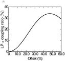
- the M 2 value of each waveguide mode of the optical fiber is 1.1 for the fundamental mode, 3.3 for the first higher-order mode, and for the second higher-order mode. 3.3, it is shown to be 3.1 for the third higher order mode. Further, when the fundamental mode and the first higher-order mode coexist, it is shown that the M 2 value changes depending on the phase relationship between the excitation ratio of the first higher-order mode and the fundamental mode. It can be seen that when the excitation ratio of the next mode is less than about 50%, the M 2 value is 2.0 or less.
- the first beam propagation method of the present embodiment is a beam propagation method in which light of 1 kW or more from a laser is propagated by 10 m or more and output from an output end, From the laser to the output end is connected by a two-mode fiber having a propagation mode number of 2 at the wavelength of the light, The light is propagated by setting the excitation ratio of the first higher-order mode of the two-mode fiber to 50% or less.
- the excitation ratio changes according to the amount of axial deviation from the center of the optical fiber.
- the reduction of the excitation ratio of the first higher-order mode to 50% or less can be sufficiently realized by the existing alignment (optical axis alignment) technique related to optical input / output.
- the second higher-order mode is cut off and a two-mode fiber having only the fundamental mode and the first higher-order mode is used, it is impossible to realize the conventional multi-mode fiber by appropriately controlling the excitation ratio.
- high-quality beam transmission with an M 2 value of 2.0 or less is possible, and a fiber design that greatly exceeds A eff, which has not been possible with conventional single-mode fibers, can be realized.
- the worst value of the M 2 value of the two-mode fiber in which only the fundamental mode and the first higher-order mode exist is 3.3, which enables relatively high-quality beam propagation compared to the multi-mode optical fiber. Fiber design is possible.
- the basis of the worst value of the M 2 value of the two-mode fiber is shown in FIG.
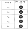
- LP01 fundamental mode
- LP11 mode M 2 is shown with respect to the excitation ratio of the LP11 mode when the (first higher order mode) are mixed
- alpha LP11 mode of the excitation ratio
- M is 0.0
- M 2 is 3.3. Since the LP11 mode is not excited 100% unless the LP11 mode is intentionally excited, the worst value of the M 2 value of the two-mode fiber is 3.3.
- the second beam propagation method of this embodiment is a beam propagation method in which light of 1 kW or more from a laser is propagated by 10 m or more and output from the output end, From the laser to the output end is connected by a 4-mode fiber having a propagation mode number of 4 at the wavelength of the light, The light is propagated by setting the excitation rate of the third higher-order mode of the four-mode fiber to 30% or less.
- Non-Patent Document 6 also shows the M 2 value when the basic mode and the third higher-order mode coexist. If the excitation ratio of the third higher-order mode falls below approximately 30%, the M 2 value becomes 2 It turns out that it becomes the following.
- the fundamental mode and the third higher-order mode are modes having an electric field peak at the center of the fiber, and the coupling efficiency changes depending on the spot size (MFD2) of light input to the fiber having the mode field diameter (MFD1).
- the vertical axis represents the efficiency with which the third higher-order mode is excited
- the horizontal axis represents the MFD difference ((MFD2 ⁇ MFD1) / MFD1) input to the fiber, and the third higher-order mode with respect to the MFD difference is excited. It is the figure which showed the relationship with the efficiency (occurrence rate of a 3rd higher mode).
- the third higher-order mode is generated according to the distance between the optical fibers (corresponding to the difference in beam diameter between the input light and the fundamental mode of the four-mode optical fiber), the fiber laser and the four-mode optical fiber And adjust the distance.
- the first higher-order mode and the second higher-order mode are higher-order modes that are generated due to the axis deviation of the fiber laser and the optical fiber, and can be sufficiently suppressed from the results of the axis deviation and the excitation amount of the first higher-order mode. is there.
- This design method determines the fiber loss and Raman gain coefficient of the photonic crystal fiber (PCF) to be used, the wavelength used for propagating light, the beam quality M2 after the PCF propagation, the laser output value, the propagation distance, and the minimum bending radius.
- PCF photonic crystal fiber
- a specification value determining step A maximum propagation mode number calculating step for calculating the maximum propagation mode number n that can be propagated using Equation 1
- An effective core area calculating step for calculating an effective core area A eff from the fiber loss and the Raman gain coefficient using Equation 2
- the bending loss at the minimum bending radius of the minimum higher-order mode to be cut off by the PCF is calculated from the hole diameter d and the interval ⁇ of the PCF, and the bending loss is shown in the graph of the horizontal axis d / ⁇ and the vertical axis ⁇ .
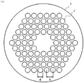
- the optical fiber according to the present embodiment has a core part and a clad part surrounding the core part, and the core part and the clad part are made of a medium having a uniform optical refractive index.
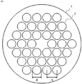
- This is a 1-cell structure photonic crystal fiber (PCF: Photonic Crystal Fiber) in which a plurality of uniform holes 2 are formed along the longitudinal direction.
- the 1-cell structure in the present invention refers to a structure of a photonic crystal having one defect in which only the central hole of the photonic crystal formed of holes arranged in a triangular lattice pattern is made of quartz. .
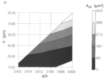
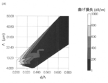
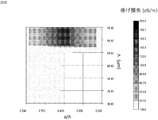
- FIG. 5 shows the range of A eff of the PCF in the region where the bending loss of the fundamental mode with a bending radius of 140 mm is 1.0 dB / m or less, where the horizontal axis is d / ⁇ and the vertical axis is ⁇ .
- the bending radius and the bending loss value in the fundamental mode are not limited to the definition or specified value of the present invention, and parameters used in the design can be determined according to necessary characteristics.
- a eff is obtained using the following equation.
- E is the electric field of light
- x and y are coordinates in the fiber cross section (assuming x and y planes), respectively.
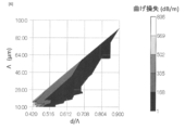
- FIG. 6 shows the bending loss of the first higher-order mode when the horizontal axis is d / ⁇ and the vertical axis is ⁇ , and the bending radius is 140 mm of the 1-cell structure PCF in light having a wavelength of 1070 nm.
- the plot range in the figure indicates a range where the bending loss in the first higher-order mode is 1 dB / m or more (a range in which the cut-off occurs).
- a (0.42, 16) B (0.42, 10) C (0.53, 10) D (0.80, 56) are set to d and ⁇ in a region surrounded by a polygon having four vertices as vertices. More specifically, when d / ⁇ is 0.724 in FIG. 6 and ⁇ is about 45 ⁇ m, Aeff is 1400 ⁇ m 2 , and the bending loss of the first higher-order mode is 40 dB / m or more, which is effectively a single mode. It turns out that it is the structure which becomes.
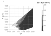
- FIG. 8 shows the third higher-order mode bending loss (1 dB / m or more) with a bending radius of 140 mm of the 1-cell structure PCF in light with a wavelength of 1070 nm, where the horizontal axis is d / ⁇ and the vertical axis is ⁇ . It is a thing.
- d / ⁇ and ⁇ that overlap the range shown in FIG. 5 and the range shown in FIG. 8, it is possible to sufficiently cut off the third higher mode and select a region where A eff is large. It becomes possible.
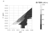
- FIG. 9 shows the fourth higher-order mode bending loss (1 dB / m or more) with a bending radius of 140 mm of the 1-cell structure PCF in the light of wavelength 1070 nm with the horizontal axis d / ⁇ and the vertical axis ⁇ . It is a thing.
- d / ⁇ and ⁇ that overlap the range shown in FIG. 5 and the range shown in FIG. 9, it is possible to select a region where the fourth higher-order mode or higher is sufficiently cut off and A eff is large. It becomes possible.
- the second higher-order mode or higher overlaps the range shown in FIG. 7, FIG. 8, or FIG. 9, the second higher-order mode or higher, the third higher-order mode or higher, The fourth higher-order mode or higher is sufficiently cut off, and it is possible to select a region where A eff is large.
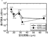
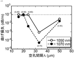
- FIG. 10 shows the wavelength dependence of the bending loss of a 1-cell PCF.
- the solid line (white circle) indicates the dependence of the fundamental mode bending loss on the gap interval ⁇ , with the wavelength of 1050 nm and the broken line (black circle) indicates the value of wavelength 7070 nm.
- the value of ⁇ is shown.
- PCF is generally known to have a characteristic that A eff is almost the same value regardless of the transmission wavelength, and the bending loss increases as the wavelength becomes shorter.
- the structure shown in FIG. 10 shows that the fundamental mode bending loss is 0.1 dB / m or less at any wavelength of 1050 nm, and that this design is effective at wavelengths of 1050 nm or more. Show.
- the optical fiber according to the present embodiment has a core part and a clad part surrounding the core part, and the core part and the clad part are made of a medium having a uniform optical refractive index.
- the PCF has a 7-cell structure in which a plurality of uniform holes 2 are formed along the longitudinal direction.
- the 7-cell structure in the present invention refers to 7 defects in which one hole in the central portion of the photonic crystal formed of holes arranged in a triangular lattice and six holes around it are made of quartz.
- FIG. 12 is a diagram illustrating A eff in a region where the horizontal axis is d / ⁇ , the vertical axis is ⁇ , and the bending loss of the fundamental mode at a bending radius of 140 mm is 1.0 dB / m or less.
- the PCF of this example has a 7-cell structure, it is advantageous in that the outer diameter of the fiber can be reduced in a region where A eff is 1000 ⁇ m 2 or more, compared with the three-layer structure of the 1-cell structure of Example 1.
- the cladding diameter needs to be 500 ⁇ m, whereas in the four-layer 7-cell structure, it can be realized with an outer diameter of about 200 ⁇ m.
- the definition of the bending loss value and the cut-off in the basic mode is not limited to the definition or specified value of the present invention, and parameters used for the design can be determined according to necessary characteristics.
- FIG. 13 shows the bending loss of the first higher-order (LP11) mode at a bending radius of 140 mm of the 7-cell structure PCF in light with a wavelength of 1070 nm, where the horizontal axis is d / ⁇ and the vertical axis is ⁇ .
- the plot range in the figure indicates a range where the bending loss in the first higher-order mode is 1 dB / m or more (a range in which the cut-off occurs).
- a (0.20, 7.80) B (0.34, 10.82) C (0.78, 48.42) are set to d / ⁇ and ⁇ in a region surrounded by a triangle having three vertices as vertices. More specifically, when d / ⁇ is 0.68 and ⁇ is about 40 ⁇ m, A eff is 5700 ⁇ m 2 , and the bending loss of the first higher-order mode is 20 dB / m or more, effectively becoming a single mode. It turns out that it is a structure.
- FIG. 14 is a graph showing the second higher-order mode bending loss (1 dB / m or more) at a bending radius of 140 mm of the 7-cell structure PCF in light of wavelength 1070 nm, where the horizontal axis is d / ⁇ and the vertical axis is ⁇ . It is.
- d / ⁇ and ⁇ that overlap the range shown in FIG. 12 and the range shown in FIG. 14, it is possible to sufficiently cut off the second higher-order mode and select a region where A eff is large. It becomes possible.
- FIG. 15 shows the third higher-order mode bending loss (1 dB / m or more) with a bending radius of 140 mm of the 1-cell structure PCF in light with a wavelength of 1070 nm, where the horizontal axis is d / ⁇ and the vertical axis is ⁇ . It is a thing.
- d / ⁇ and ⁇ that overlap the range shown in FIG. 12 and the range shown in FIG. 15, it is possible to sufficiently cut off the third higher-order mode and select a region where A eff is large. It becomes possible.
- FIG. 16 shows the fourth higher-order mode bending loss (1 dB / m or more) when the horizontal axis is d / ⁇ and the vertical axis is ⁇ , and the bending radius is 140 mm of the 1-cell structure PCF in light having a wavelength of 1070 nm. It is a thing.
- d / ⁇ and ⁇ that overlap the range shown in FIG. 12 and the range shown in FIG. 16, it is possible to select a region where the fourth higher-order mode or higher is sufficiently cut off and A eff is large. It becomes possible.
- the second higher-order mode or higher overlaps the range shown in FIG. 14, FIG. 15, or FIG. 16, the second higher-order mode or higher, the third higher-order mode or higher, The fourth higher-order mode or higher is sufficiently cut off, and it is possible to select a region where A eff is large.
- FIG. 17 shows the wavelength dependence of the bending loss of a 7-cell PCF.
- the solid line (white circle) indicates the dependence of the fundamental mode bending loss on the gap interval ⁇ , with the wavelength of 1050 nm and the broken line (black circle) indicates the value of wavelength 7070 nm.
- the value of ⁇ is shown.
- PCF is generally known to have a characteristic that A eff is almost the same value regardless of the transmission wavelength, and the bending loss increases as the wavelength becomes shorter.
- the structure shown in FIG. 17 shows that the fundamental mode bending loss is 0.1 dB / m or less at any wavelength of 1050 nm, and that this design is effective at wavelengths of 1050 nm or more. Show.
- the optical fiber design method of this embodiment is Determination of specification values for determining fiber loss and Raman gain coefficient of photonic crystal fiber (PCF) to be used, wavelength used for propagating light, beam quality M 2 after propagation of PCF, laser output value, propagation distance, and minimum bending radius Steps, A maximum propagation mode number calculating step for calculating the maximum propagation mode number n that can be propagated using Equation 1, An effective core area calculating step for calculating an effective core area A eff from the fiber loss and the Raman gain coefficient using Equation 2, A fiber structure calculating step for calculating the diameter and interval of the holes of the PCF satisfying the A eff ; A bending loss calculating step of calculating a bending loss at a minimum bending radius with the PCF of the structure calculated in the fiber structure calculating step, and calculating
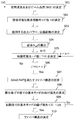
- FIG. 18 is a flowchart showing the procedure of the optical fiber design method of the present embodiment.
- step S01 specifically value determining step determines the beam quality to use wavelength and the target (M 2 value).
- step S02 largest propagation mode number calculation step
- step S04 calculates the largest number propagation mode which can satisfy M 2 value of step S01 from Equation (1) (wherein the non-patent document 6 (17))
- the most propagation mode number n is determined.
- the output power and propagation distance used in step S03 are determined, and in step S04 (effective core area calculation step), equation (2) (shown in Non-Patent Document 7).
- the required effective core area (A eff ) is calculated using the SRS threshold definition formula (8.1.13)).
- step S05 the number of modes that can be propagated (1 + k) is determined.
- step S08 bending loss calculation step
- the bending loss of the fundamental mode at the minimum bending radius used in the fiber structure designed in step S07 is calculated.
- step S09 If the specified value in step S09 is exceeded, the process returns to step S05 and the propagation possible mode The number is incremented by 1 and the procedure up to step S09 is repeated (mode increasing step). At this time, if the number of modes 1 + k exceeds the maximum number of propagation modes n in step S06, there is no solution of the fiber structure that satisfies the set beam quality with the output power and propagation distance, so the process returns to step S01 to return the beam quality (M review the specification value of 2 values) and the like, to determine the fiber structure by repeating the steps S02 follows.
- a specification value is determined as step S01. here, Fiber loss: 1 dB / km (fiber transmission loss at the following wavelengths)
- Raman gain coefficient g R 8.79 ⁇ 10 ⁇ 12 (cm / W)
- Wavelength ⁇ used for propagating light 1070 nm
- Beam quality M 2 1.5 or less
- Laser output value 100 W
- Propagation distance 300m
- Minimum bending radius 140m
- the Raman gain coefficient gR was calculated using Equation (4) (Equation (36) shown in Non-Patent Document 8).
- step S04 the required A eff is calculated as approximately 160 ⁇ m 2 from the equation (2) (Note that the SRS threshold used in the equation (2) is the output power determined in step S03). Since the SRS threshold value calculated from Equation (2) varies depending on the fiber loss and g R , the required A eff also varies. For this reason, the fiber loss and g R are not limited to the present contents, but are appropriately changed depending on the fiber material to be used.
- step S05 fiber structure design is performed in a single mode (the number of modes that can be propagated is 1).
- the structural design of the PCF can be performed by the structural analysis by the finite element method shown in Non-Patent Document 9 or the approximate analysis shown by Non-Patent Document 10, and in this embodiment, the structural analysis by the finite element method is performed. Using.
- the analysis method is not limited to the present embodiment, and a technique capable of analyzing the structure of the fiber may be used as appropriate.
- the analysis was performed using the finite element method.
- the minimum bending radius is 140 mm
- the bending loss of the fundamental mode is calculated as 1 ⁇ 10 ⁇ 4 dB / m at R140 mm in the above structure. Since the propagation distance is 300 m, the total bending loss is 0.03 dB.
- step S09 it is confirmed whether the bending loss value at the propagation length is 0.1 dB or less. As described above, since the bending loss after 300 m propagation is 0.03 dB, the requirement of Step S09 is satisfied, and the fiber structure is determined by this structure (Step S10).
- the confinement loss of the first higher-order mode is 6 dB / m or more, this structure operates in a single mode, causing a slight axis shift, and even after the first higher-order mode is excited, after 300 m propagation.
- the first higher-order mode has a sufficiently small excitation ratio due to bending loss.
- the above description is an example of the structure calculated using the design flow of FIG. 18, and the fiber parameters may be appropriately determined using this design flow according to the target beam quality, output power, and propagation distance.
- the maximum output power (SRS threshold) and the Leff interaction length are inversely related.
- the optical fiber of the present invention assumes a relatively short transmission distance of 1 km or less, and Leff and propagation distance L are equivalent. Therefore, in this specification, the output power performance is described as the product of output power and propagation distance (kW ⁇ m). Note that the transmission distance is not limited to 1 km or less, and can be similarly applied as long as Leff and L can be regarded as equivalent.
- Embodiments 5 to 8 will be described with reference to FIGS.
- the figure shows a region where the desired PCF parameter is d / ⁇ on the horizontal axis and ⁇ on the vertical axis.
- (a) coordinates under the condition of M 2 ⁇ 2.0 are A1 (0.42, 16.88) A2 (0.48, 25.31) A3 (0.57, 40.00) B (0.42, 10.94) C1 (0.60, 15.63) C2 (0.69, 31.88) C3 (0.76, 47.81) D (0.74, 43.12) E (0.75, 44.38) F (0.81, 60.63) G (0.85, 60.63) H (0.85, 77.50) I (0.90, 91.88), (B) The coordinates under the condition of M 2 ⁇ 3.3 are A1 (0.42, 16.88) A2 (0.47, 25.31) A3 (0.56, 40.00) B (0.42, 10.94) C1 (0.75, 15.00) C
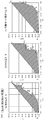
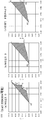
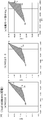
- FIG. 19 shows that when light having a wavelength of 1070 nm is propagated, d / ⁇ and ⁇ satisfying (a) M 2 ⁇ 2.0, (b) M 2 ⁇ 3.3, and (c) the number of propagation modes is 4 or less. It is a figure explaining the relationship of Aeff (160 micrometers 2 or more).
- the plotted area (area shown by diagonal lines) has a structure capable of transmitting 30 kW ⁇ m in a 1-cell PCF.
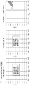
- FIG. 20 shows that when light having a wavelength of 1070 nm is propagated, (a) M 2 ⁇ 2.0, (b) M 2 ⁇ 3.3, and (c) d / ⁇ and ⁇ satisfying the number of propagation modes of 4 or less. It is a figure explaining the relationship of Aeff (800 micrometers 2 or more).
- the plotted area (area shown by hatching) has a structure capable of 150 kW ⁇ m in a 1-cell PCF.
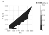
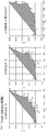
- FIG. 21 shows that when light having a wavelength of 1070 nm is propagated, (a) M 2 ⁇ 2.0, (b) M 2 ⁇ 3.3, and (c) d / ⁇ and ⁇ satisfying a propagation mode number of 4 or less. It is a figure explaining the relationship of Aeff (1600 micrometers 2 or more).
- the plotted area (area shown by diagonal lines) has a structure capable of 300 kW ⁇ m transmission in a 1-cell PCF.
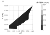
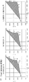
- FIG. 22 shows that when propagating light having a wavelength of 1070 nm, (a) M 2 ⁇ 2.0, (b) M 2 ⁇ 3.3, and (c) d / ⁇ and ⁇ satisfying a propagation mode number of 4 or less. It is a figure explaining the relationship of Aeff (3200 micrometers 2 or more).
- the plotted area (the area shown by hatching) has a structure capable of transmitting 600 kW ⁇ m in a 1-cell PCF.
- d / ⁇ and ⁇ are set in a region surrounded by polygons with A4, J1, and K as vertices.
- Embodiments 9 to 13 will be described with reference to FIGS.
- the figure shows a region where the desired PCF parameter is d / ⁇ on the horizontal axis and ⁇ on the vertical axis.
- (a) coordinates in M 2 ⁇ 2.0 are A1 (0.20, 10.98) A2 (0.21, 11.77) A3 (0.27, 16.06) A4 (0.40, 24.46) A5 (0.53, 32.87) B (0.20, 4.95) C1 (0.25, 5.27) C2 (0.40, 12.88) C3 (0.60, 20.34) C4 (0.68, 29.56) C5 (0.72, 36.35) D (0.29, 9.87) E (0.40, 12.25) F (0.40, 13.52) G (0.49, 14.15) H (0.49, 15.74) I (0.50, 18.12) J (0.58, 18.12) K (0.58, 19.86) L (0.60, 23.03) M (0.68, 23.99) N
- A2 (0.21, 11.77) A3 (0.27, 16.06) A4 (0.40, 24.78) A5 (0.53, 32.87) B (0.20, 5.11) C (0.50, 6.23) D (0.50, 10.00) E (0.60, 15.18) F (0.60, 17.76) G (0.65, 20.12) H (0.70, 20.35) I (0.79, 25.06) J (0.79, 29.53) K (0.78, 29.76) K1 (0.78, 30.66) L (0.78, 38.29) M (0.80, 40.12) N (0.80, 50.00) Will be described.
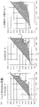
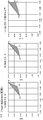
- FIG. 23 shows that when light having a wavelength of 1070 nm is propagated, (a) M 2 ⁇ 2.0, (b) M 2 ⁇ 3.3, (c) d / ⁇ and ⁇ satisfying the number of propagation modes of 4 or less. It is a figure explaining the relationship of Aeff (160 micrometers 2 or more).
- the plotted area (area shown by slanting lines) has a structure capable of transmitting 30 kW ⁇ m in a 7-cell PCF.
- Embodiment 12 [7cell structure 600kW ⁇ m transmission]
- the range of PCF parameters ( ⁇ and d) of the 7-cell structure in FIG. 11 that enables 600 kW ⁇ m transmission will be described.
- FIG. 26 when propagating light having a wavelength of 1070 nm, (a) M 2 ⁇ 2.0, (b) M 2 ⁇ 3.3, and (c) d / ⁇ and ⁇ satisfying the number of propagation modes of 4 or less. It is a figure explaining the relationship of Aeff (3200 micrometers 2 or more).
- the plotted area (area shown by diagonal lines) has a structure capable of transmitting 600 kW ⁇ m in a 7-cell PCF.
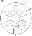
- FIG. 28 shows a structural example of the PCF of this embodiment.
- the PCF of this embodiment shows an optical fiber structure configured with fewer holes than the PCF of FIG.
- the core region is one vacancy defect and the number of vacancies is 12, as in FIG.
- the accuracy of the position and size of each hole affects the optical characteristics, and as the number of holes increases, the difficulty of manufacture and the deterioration of the structure yield become more prominent.
- the structure shown in FIG. 28 is preferable because light wave guiding is realized with a simple structure having 12 or less holes, so that mass productivity is high and controllability at the time of manufacturing optical characteristics is improved.
- the PCF structure shown in FIG. 28 can transmit high-quality and kW-class high-power light having an M2 of 2.0 or less within a predetermined design range.
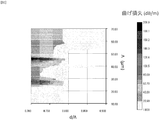
- FIG. 29 shows a structural range in which the bending loss with respect to the fundamental mode is 0.1 dB / m or less.
- FIG. 31 and FIG. 32 show bending loss values for the LP11 mode, LP21 mode, and LP02 mode, respectively, and the loss of the target mode becomes sufficiently large in the region surrounded by the frame (bending loss of 1 dB / m or more). Can be leaked.
- the LP02 mode is cut off, and the amount of misalignment between the laser oscillation unit and the PCF is kept below a certain level, so that high quality and high power output light can be obtained. Therefore, the object can be achieved in the overlapping range of FIG. 29 and FIG. 32 shown in FIG. That is, a structure in which ⁇ is 50 ⁇ m to 65 ⁇ m and d / ⁇ is 0.79 to 0.88, or ⁇ is 50 ⁇ m and d / ⁇ is 0.7 to 0.79 is preferable. At this time, since the number of vacancies is as small as 12, the manufacturing yield and accuracy are extremely good, and M2 of 2.0 or less and kW-class output light can be obtained, which is preferable.
- the predetermined number of modes is 3, and the basic modes LP01, LP11, and LP21 are propagated and the LP02 is not propagated.
- the present invention is not limited to this.
- the predetermined number of modes may be 2, and the LP01 mode and the LP11 mode may be propagated, and the mode higher than the LP21 mode may not be propagated. As a result, the same effect as in the present embodiment can be obtained.
- FIGS. 30 and 32 show a structure in which the LP11 mode and the LP21 mode leak, and the number of modes is set to 2 using the overlapping region of FIGS. 29 and 30, and the overlapping region of FIGS. 29 and 32 is used.
- the number of modes can be set to 3. That is, ⁇ is 30 ⁇ m to 55 ⁇ m and d / ⁇ is 0.70 to 0.79, or ⁇ is 55 ⁇ m to 65 ⁇ m and d / ⁇ is 0.79 to 0.83, or ⁇ is 57 ⁇ m to 65 ⁇ m.
- the number of modes is set to 2 by adopting a structure in which d / ⁇ is 0.83 or more and 0.88 or less, or ⁇ is 59 ⁇ m or more and 68 ⁇ m or less and d / ⁇ is 0.88 or more and 0.89 or less. be able to. Further, by setting ⁇ to 52 ⁇ m or more and 65 ⁇ m or less and d / ⁇ being 0.79 to 0.88, or ⁇ being 52 ⁇ m or less and d / ⁇ being 0.7 to 0.77, Can be set to 3.
- the present invention uses the definition formula of the SRS threshold for the required output power and propagation distance, and the required beam quality (when the propagation mode is uniformly excited from the bending loss and the number of modes that can be propagated).
- a fiber structure that satisfies the threshold value can be designed using the M 2 value of N.
- the specific structure of a high-quality high-power transmission optical fiber can be clarified using the design flow.
- An example of the structure of the PCF is shown as a specific design example.
- the optical fiber and the optical fiber design method according to the present invention it is possible to secure the output power with respect to the propagation length at a desired beam quality that cannot be realized by the conventional design. It becomes possible to provide a possible optical fiber.
- the fiber structure designed using the design flow used in the present invention can satisfy the required output power, propagation distance, and beam quality.
- the beam quality can be improved. It is possible to realize use of light with a good propagation distance.
- the present invention can be applied to the field of laser processing using a fiber laser.
Landscapes
- Physics & Mathematics (AREA)
- General Physics & Mathematics (AREA)
- Optics & Photonics (AREA)
- Chemical & Material Sciences (AREA)
- Dispersion Chemistry (AREA)
- Lasers (AREA)
- Optical Couplings Of Light Guides (AREA)
- Optical Fibers, Optical Fiber Cores, And Optical Fiber Bundles (AREA)
Abstract
Description
使用するフォトニッククリスタルファイバ(PCF)のファイバ損失及びラマン利得係数、伝搬する光の使用波長、前記PCF伝搬後のビーム品質M2、レーザ出力値、伝搬距離、最小曲げ半径を決定する仕様値決定ステップと、
数1を用いて伝搬可能な最多伝搬モード数nを算出する最多伝搬モード数算出ステップと、
数2を用いてファイバ損失及びラマン利得係数から実効コア断面積Aeffを算出する実効コア断面積算出ステップと、
前記Aeffを満たすPCFの空孔の直径dと間隔Λを計算するファイバ構造算出ステップと、
前記ファイバ構造算出ステップで計算した構造のPCFで最小曲げ半径での曲げ損失を計算し、前記伝搬距離から伝搬長の曲げ損失を計算する曲げ損失計算ステップと、
前記伝搬長の曲げ損失が所定値未満であることを確認し、前記ファイバ構造算出ステップで計算したPCFの構造を確定する確認ステップと、
前記確認ステップで前記伝搬長の曲げ損失が所定値以上である場合、モード数を1つ増やして前記ファイバ構造算出ステップ、前記曲げ損失計算ステップ、及び前記確認ステップを、モード数が最多伝搬モード数nに達するまで繰り返すモード増加ステップと、
を行う。
数1と数2については後述する。
すなわち、本発明に係る光ファイバ設計方法は、
使用するフォトニッククリスタルファイバ(PCF)のファイバ損失及びラマン利得係数、伝搬する光の使用波長、前記PCF伝搬後のビーム品質M2、レーザ出力値、伝搬距離、最小曲げ半径を決定する仕様値決定ステップと、
数1を用いて伝搬可能な最多伝搬モード数nを算出する最多伝搬モード数算出ステップと、
数2を用いてファイバ損失及びラマン利得係数から実効コア断面積Aeffを算出する実効コア断面積算出ステップと、
前記Aeff以上となるPCFの空孔の直径dと間隔Λを計算し、横軸d/Λ、縦軸Λのグラフに前記Aeff以上となる点をプロットするファイバ構造算出ステップと、
PCFの空孔の直径dと間隔Λから該PCFでカットオフさせる最小の高次モードの最小曲げ半径での曲げ損失を計算し、横軸d/Λ、縦軸Λのグラフに該曲げ損失が1dB/m以上となる点をプロットする曲げ損失計算ステップと、
前記ファイバ構造算出ステップでグラフにプロットした点の領域と前記曲げ損失計算ステップでグラフにプロットした点の領域とが重複する重複範囲を検出し、前記重複範囲にある直径dと間隔Λの空孔を持つPCF構造に決定する構造決定ステップと、
を行う。
数1と数2については後述する。
当該PCFは、光の伝搬方向に直径dの空孔が間隔Λで配列する1cell構造のPCFであって、
座標(d/Λ,Λ)としたとき、
A1(0.42,16.88)
B(0.42,10.94)
C1(0.60,15.63)
C2(0.69,31.88)
D(0.74,43.12)
E(0.75,44.38)
C3(0.76,47.81)
F(0.81,60.63)
G(0.85,60.63)
H(0.85,77.50)
I(0.90,91.88)
を頂点とする多角形で囲まれる領域にある直径dと間隔Λの空孔を持つことを特徴とする。
第1高次モード以上を十分にカットオフしつつ、Aeffをできるだけ大きくすることができる。
当該PCFは、光の伝搬方向に直径dの空孔が間隔Λで配列する1cell構造のPCFであって、
座標(d/Λ,Λ)としたとき、
A1(0.42,16.88)
B(0.42,10.94)
C1(0.75,15.00)
D1(0.75,20.00)
C2(0.78,35.00)
D2(0.80,35.93)
E(0.80,45.63)
F(0.83,51.56)
C3(0.90,54.38)
I(0.90,91.88)
を頂点とする多角形で囲まれる領域にある直径dと間隔Λの空孔を持つことを特徴とする。
第3高次モード以上を十分にカットオフしつつ、Aeffをできるだけ大きくすることができる。
当該PCFは、光の伝搬方向に直径dの空孔が間隔Λで配列する1cell構造のPCFであって、
座標(d/Λ,Λ)としたとき、
A1 (0.42,16.88)
B (0.42,10.94)
C (0.75,14.24)
D (0.75,12.10)
E (0.79,20.00)
F (0.85,30.00)
G (0.85,41.58)
H (0.89,50.00)
I (0.89,58.95)
J (0.90,60.0)
K (0.90,91.88)
を頂点とする多角形で囲まれる領域にある直径dと間隔Λの空孔を持つことを特徴とする。
第4高次モード以上を十分にカットオフしつつ、Aeffをできるだけ大きくすることができる。
当該PCFは、光の伝搬方向に直径dの空孔が間隔Λで配列する7cell構造のPCFであって、
座標(d/Λ,Λ)としたとき、
A1(0.20,10.98)
B(0.20,4.95)
C1(0.25,5.27)
D(0.29,9.87)
E(0.40,12.25)
F(0.40,13.52)
G(0.49,14.15)
H(0.49,15.74)
I(0.50,18.12)
J(0.58,18.12)
K(0.58,19.86)
C3(0.60,20.34)
L(0.60,23.03)
M(0.68,23.99)
N(0.68,31.60)
O(0.79,48.73)
P(0.80,50.00)
を頂点とする多角形で囲まれる領域にある直径dと間隔Λの空孔を持つことを特徴とする。
第1高次モード以上を十分にカットオフしつつ、Aeffをできるだけ大きくすることができる。
当該PCFは、光の伝搬方向に直径dの空孔が間隔Λで配列する7cell構造のPCFであって、
座標(d/Λ,Λ)としたとき、
A1(0.20,10.98)
B(0.20,5.11)
C1(0.40,5.90)
D(0.40,10.03)
E(0.50,11.93)
F(0.50,14.47)
C3(0.60,20.18)
G(0.69,22.08)
H(0.68,23.67,)
I(0.70,24.30)
J(0.70,32.87)
K(0.80,50.00)
を頂点とする多角形で囲まれる領域にある直径dと間隔Λの空孔を持つことを特徴とする。
第3高次モード以上を十分にカットオフしつつ、Aeffをできるだけ大きくすることができる。
当該PCFは、光の伝搬方向に直径dの空孔が間隔Λで配列する7cell構造のPCFであって、
座標(d/Λ,Λ)としたとき、
A1 (0.20,10.98)
B (0.20,5.11)
C (0.50,6.23)
D (0.50,10.00)
E (0.60,15.18)
F (0.60,17.76)
G (0.65,20.12)
H (0.70,20.35)
I (0.79,25.06)
J (0.79,29.53)
K (0.78,29.76)
L (0.78,38.29)
M (0.80,40.12)
N (0.80,50.00)
を頂点とする多角形で囲まれる領域にある直径dと間隔Λの空孔を持つことを特徴とする。
第4高次モード以上を十分にカットオフしつつ、Aeffをできるだけ大きくすることができる。
本ビーム伝搬方法は、レーザからの1kW以上の光を10m以上伝搬させて出力端から出力させるビーム伝搬方法であって、
前記レーザから前記出力端までを、前記光の波長において伝搬モード数が2である2モードファイバで接続し、
前記2モードファイバの第1高次モードの励振比率を50%以下として光を伝搬させることを特徴とする。
前記レーザから前記出力端までを、前記光の波長において伝搬モード数が4以下である4モードファイバで接続し、
前記4モードファイバの第3高次モードの励振率を30%以下として光を伝搬させることを特徴とする。
本発明の特徴は、Aeffを拡大することによる出力パワーの向上および伝送距離の長延化を図ることである。本発明の従来技術との大きな違いは、光ファイバが複数モードが伝搬可能な構造である点である。本発明は、入力部で高次モードが励振される効率を十分に低減し、M2を十分に小さい値にすることが可能な領域を明らかにして、Aeffを従来では実現できなかった値にすることを可能とした。
前記レーザから前記出力端までを、前記光の波長において伝搬モード数が2である2モードファイバで接続し、
前記2モードファイバの第1高次モードの励振比率を50%以下として光を伝搬させることを特徴とする。
前記レーザから前記出力端までを、前記光の波長において伝搬モード数が4である4モードファイバで接続し、
前記4モードファイバの第3高次モードの励振率を30%以下として光を伝搬させることを特徴とする。
本実施形態は、図4に示す空孔2を有する1cellコア構造のPCFにおいて、実効コア断面積Aeffの拡大と既定の曲げ損失αbを実現するための構造パラメータ(空孔2の直径dと空孔2の間隔Λ)の設計方法に関する。本実施例では、基本モードの最小曲げ半径、及び高次モードの実効カットオフを規定する曲げ半径を140mmで説明をしているが、本方法はこれに制限されるものではない。
数1を用いて伝搬可能な最多伝搬モード数nを算出する最多伝搬モード数算出ステップと、
数2を用いてファイバ損失及びラマン利得係数から実効コア断面積Aeffを算出する実効コア断面積算出ステップと、
前記Aeff以上となるPCFの空孔の直径dと間隔Λを計算し、横軸d/Λ、縦軸Λのグラフに前記Aeff以上となる点をプロットするファイバ構造算出ステップと、
PCFの空孔の直径dと間隔Λから該PCFでカットオフさせる最小の高次モードの最小曲げ半径での曲げ損失を計算し、横軸d/Λ、縦軸Λのグラフに該曲げ損失が1dB/m以上となる点をプロットする曲げ損失計算ステップと、
前記ファイバ構造算出ステップでグラフにプロットした点の領域と前記曲げ損失計算ステップでグラフにプロットした点の領域とが重複する重複範囲を検出し、前記重複範囲にある直径dと間隔Λの空孔を持つPCF構造に決定する構造決定ステップと、
を行う。
数1と数2については後述する。

A(0.42,16)
B(0.42,10)
C(0.53,10)
D(0.80,56)
の4点を頂点とする多角形で囲まれる領域内のd及びΛに設定する。
さらに具体的には、図6でd/Λが0.724とし、Λが45μm程度にするとAeffが1400μm2、第1高次モードの曲げ損失が40dB/m以上になり実効的に単一モードになる構造であることがわかる。
A(0.42,16)
B(0.42,10)
C(0.76,10)
D(0.80,56)
の4点を頂点とする多角形で囲まれる領域内のd及びΛに設定する。
A(0.42,16)
B(0.42,10)
C(0.76,10)
D(0.80,56)
の4点を頂点とする多角形で囲まれる領域内のd及びΛに設定する。
A(0.42,16)
B(0.42,10)
C(0.76,10)
D(0.80,56)
の4点を頂点とする多角形で囲まれる領域内のd及びΛに設定する。
本実施形態は、図11に示すような複数の空孔2を有する7cellコア構造のPCFにおいて、Aeffの拡大と既定の曲げ損失αbを実現するための構造パラメータ(空孔2の直径dと空孔2の間隔Λ)の設計方法に関する。本設計方法も実施形態2で説明した設計方法を利用する。
A(0.20,7.80)
B(0.34,10.82)
C(0.78,48.42)
の3点を頂点とする三角形で囲まれる領域内のd/Λ及びΛに設定する。
さらに具体的には、d/Λが0.68とし、Λが40μm程度にするとAeffが5700μm2、第1高次モードの曲げ損失が20dB/m以上になり実効的に単一モードになる構造であることがわかる。
A(0.20,7.80)
B(0.20,4.00)
C(0.80,4.00)
D(0.80,50.0)
の4点を頂点とする多角形で囲まれる領域内のd/Λ及びΛに設定する。
A(0.20,7.80)
B(0.20,4.00)
C(0.80,4.00)
D(0.80,50.0)
の4点を頂点とする多角形で囲まれる領域内のd/Λ及びΛに設定する。
A(0.20,7.80)
B(0.20,4.00)
C(0.80,4.00)
D(0.80,50.0)
の4点を頂点とする多角形で囲まれる領域内のd/Λ及びΛに設定する。
本実施形態では、実施形態1~3で説明した2モードファイバや4モードファイバを、レーザー加工システム等の光伝送媒体としての仕様に基づいて設計する他の設計方法を説明する。本実施形態の光ファイバ設計方法は、
使用するフォトニッククリスタルファイバ(PCF)のファイバ損失及びラマン利得係数、伝搬する光の使用波長、前記PCF伝搬後のビーム品質M2、レーザ出力値、伝搬距離、最小曲げ半径を決定する仕様値決定ステップと、
数1を用いて伝搬可能な最多伝搬モード数nを算出する最多伝搬モード数算出ステップと、
数2を用いてファイバ損失及びラマン利得係数から実効コア断面積Aeffを算出する実効コア断面積算出ステップと、
前記Aeffを満たすPCFの空孔の直径と間隔を計算するファイバ構造算出ステップと、
前記ファイバ構造算出ステップで計算した構造のPCFで最小曲げ半径での曲げ損失を計算し、前記伝搬距離から伝搬長の曲げ損失を計算する曲げ損失計算ステップと、
前記伝搬長の曲げ損失が例えば0.1dB未満であることを確認し、前記ファイバ構造算出ステップで計算したPCFの構造を確定する確認ステップと、
前記確認ステップで前記伝搬長の曲げ損失が例えば0.1dB以上である場合、モード数を1つ増やして前記ファイバ構造算出ステップ、前記曲げ損失計算ステップ、及び前記確認ステップを、モード数が最多伝搬モード数nに達するまで繰り返すモード増加ステップと、
を行う。
その後に、ステップS03(仕様値決定ステップ)にて使用する出力パワー、伝搬距離を決定し、ステップS04(実効コア断面積算出ステップ)において、数式(2)(非特許文献7に示されているSRS閾値定義式(8.1.13))を用いて必要な実効コア断面積(Aeff)を算出する。
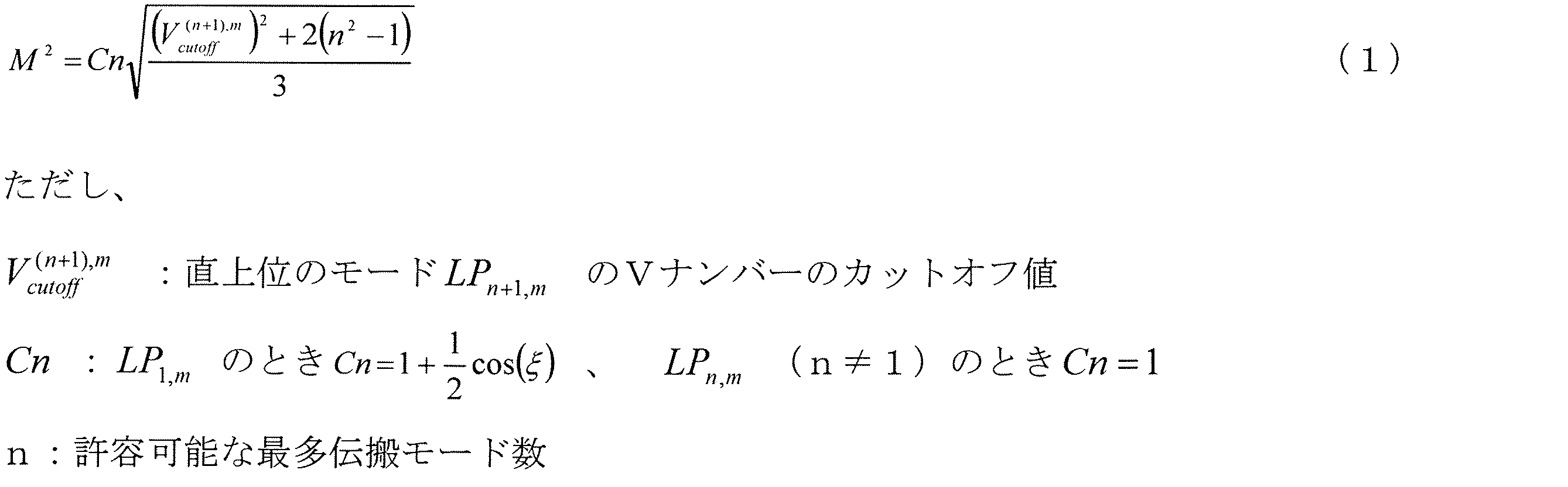

まず、ステップS01として仕様値を決定する。ここでは、
ファイバ損失:1dB/km(下記波長におけるファイバの伝送損失)
ラマン利得係数gR:8.79×10⁻¹²(cm/W)
伝搬する光の使用波長λ:1070nm
ビーム品質M2:1.5以下
レーザ出力値:100W
伝搬距離:300m
最小曲げ半径:140m
とする。なお、ラマン利得係数gRは数式(4)(非特許文献8に示される式(36))を用いて算出した。

実施形態5から8を図19から図22を用いて説明する。当該図は、所望性のPCFのパラメータを横軸にd/Λ、縦軸にΛとしたときの領域を示している。ここで、(a)M2≦2.0の条件における座標を
A1(0.42,16.88)
A2(0.48,25.31)
A3(0.57,40.00)
B(0.42,10.94)
C1(0.60,15.63)
C2(0.69,31.88)
C3(0.76,47.81)
D(0.74,43.12)
E(0.75,44.38)
F(0.81,60.63)
G(0.85,60.63)
H(0.85,77.50)
I(0.90,91.88)とし、
(b)M2≦3.3の条件における座標を
A1(0.42,16.88)
A2(0.47,25.31)
A3(0.56,40.00)
B(0.42,10.94)
C1(0.75,15.00)
C2(0.78,35.00)
C3(0.90,54.38)
D1(0.75,20.00)
D2(0.80,35.93)
E(0.80,45.63)
F(0.83,51.56)
I(0.90,91.88)
(c)伝搬モード数が4以下の条件における座標を
A1(0.42,16.88)
A2(0.48,25.31)
A3(0.57,40.00)
A4(0.75,68.36)
B(0.42,10.94)
C(0.75,14.24)
D(0.75,12.10)
E(0.79,20.00)
F(0.85,30.00)
F1(0.85,36.37)
G(0.85,41.58)
H(0.89,50.00)
H1(0.89,54.37)
I(0.89,58.95)
J(0.90,60.0)
J1(0.90,77.07)
K(0.90,91.88)
として説明する。
[1cell構造 30kW・m伝送]
本実施形態は、30kW・m伝送を可能とする図4の1cell構造のPCFパラメータ(Λとd)の範囲を説明する。図19は、波長1070nmの光を伝搬させるとき、(a)M2≦2.0、(b)M2≦3.3、(c)伝搬モード数が4以下を満たすd/ΛとΛとAeff(160μm2以上)の関係を説明する図である。プロットされた領域(斜線で示した領域)は、1cell構造のPCFにおいて30kW・m伝送できる構造になる。
[1cell構造 150kW・m伝送]
本実施形態は、150kW・m伝送を可能とする図4の1cell構造のPCFパラメータ(Λとd)の範囲を説明する。図20は、波長1070nmの光を伝搬させるとき、(a)M2≦2.0、(b)M2≦3.3、(c)伝搬モード数が4以下を満たすd/ΛとΛとAeff(800μm2以上)の関係を説明する図である。プロットされた領域(斜線で示した領域)は、1cell構造のPCFにおいて150kW・mできる構造になる。
[1cell構造 300kW・m伝送]
本実施形態は、300kW・m伝送を可能とする図4の1cell構造のPCFパラメータ(Λとd)の範囲を説明する。図21は、波長1070nmの光を伝搬させるとき、(a)M2≦2.0、(b)M2≦3.3、(c)伝搬モード数が4以下を満たすd/ΛとΛとAeff(1600μm2以上)の関係を説明する図である。プロットされた領域(斜線で示した領域)は、1cell構造のPCFにおいて300kW・m伝送できる構造になる。
[1cell構造 600kW・m伝送]
本実施形態は、600kW・m伝送を可能とする図4の1cell構造のPCFパラメータ(Λとd)の範囲を説明する。図22は、波長1070nmの光を伝搬させるとき、(a)M2≦2.0、(b)M2≦3.3、(c)伝搬モード数が4以下を満たすd/ΛとΛとAeff(3200μm2以上)の関係を説明する図である。プロットされた領域(斜線で示した領域)は、1cell構造のPCFにおいて600kW・m伝送できる構造になる。
実施形態9から13を図23から図27を用いて説明する。当該図は、所望性のPCFのパラメータを横軸にd/Λ、縦軸にΛとしたときの領域を示している。ここで、(a)M2≦2.0における座標を
A1(0.20,10.98)
A2(0.21,11.77)
A3(0.27,16.06)
A4(0.40,24.46)
A5(0.53,32.87)
B(0.20,4.95)
C1(0.25,5.27)
C2(0.40,12.88)
C3(0.60,20.34)
C4(0.68,29.56)
C5(0.72,36.35)
D(0.29,9.87)
E(0.40,12.25)
F(0.40,13.52)
G(0.49,14.15)
H(0.49,15.74)
I(0.50,18.12)
J(0.58,18.12)
K(0.58,19.86)
L(0.60,23.03)
M(0.68,23.99)
N(0.68,31.60)
O(0.79,48.73)
P(0.80,50.00)とし、
(b)M2≦3.3における座標を
A1(0.20,10.98)
A2(0.21,11.77)
A3(0.27,16.06)
A4(0.40,24.78)
A5(0.53,32.87)
B(0.20,5.11)
C1(0.40,5.90)
C2(0.50,13.68)
C3(0.60,20.18)
C4(0.70,30.01)
C5(0.73,37.00)
D(0.40,10.03)
E(0.50,11.93)
F(0.50,14.47)
C3(0.60,20.18)
G(0.69,22.08)
H(0.68,23.67,)
I(0.70,24.30)
J(0.70,32.87)
K(0.80,50.00)
(c)伝搬モード数が4以下の条件における座標を
A1(0.20,10.98)
A2(0.21,11.77)
A3(0.27,16.06)
A4(0.40,24.78)
A5(0.53,32.87)
B(0.20,5.11)
C(0.50,6.23)
D(0.50,10.00)
E(0.60,15.18)
F(0.60,17.76)
G(0.65,20.12)
H(0.70,20.35)
I(0.79,25.06)
J(0.79,29.53)
K(0.78,29.76)
K1(0.78,30.66)
L(0.78,38.29)
M(0.80,40.12)
N(0.80,50.00)
として説明する。
[7cell構造 30kW・m伝送]
本実施形態は、30kW・m伝送を可能とする図10の7cell構造のPCFパラメータ(Λとd)の範囲を説明する。図23は、波長1070nmの光を伝搬させるとき、(a)M2≦2.0、(b)M2≦3.3、(c)伝搬モード数が4以下を満たすd/ΛとΛとAeff(160μm2以上)の関係を説明する図である。プロットされた領域(斜線で示した領域)は、7cell構造のPCFにおいて30kW・m伝送できる構造になる。
[7cell構造 150kW・m伝送]
本実施形態は、150kW・m伝送を可能とする図11の7cell構造のPCFパラメータ(Λとd)の範囲を説明する。図24は、波長1070nmの光を伝搬させるとき、(a)M2≦2.0、(b)M2≦3.3、(c)伝搬モード数が4以下を満たすd/ΛとΛとAeff(800μm2以上)の関係を説明する図である。プロットされた領域(斜線で示した領域)は、7cell構造のPCFにおいて150kW・m伝送できる構造になる。
[7cell構造 300kW・m伝送]
本実施形態は、300kW・m伝送を可能とする図11の7cell構造のPCFパラメータ(Λとd)の範囲を説明する。図25は、波長1070nmの光を伝搬させるとき、(a)M2≦2.0、(b)M2≦3.3、(c)伝搬モード数が4以下を満たすd/ΛとΛとAeff(1600μm2以上)の関係を説明する図である。プロットされた領域(斜線で示した領域)は、7cell構造のPCFにおいて300kW・m伝送できる構造になる。
[7cell構造 600kW・m伝送]
本実施形態は、600kW・m伝送を可能とする図11の7cell構造のPCFパラメータ(Λとd)の範囲を説明する。図26は、波長1070nmの光を伝搬させるとき、(a)M2≦2.0、(b)M2≦3.3、(c)伝搬モード数が4以下を満たすd/ΛとΛとAeff(3200μm2以上)の関係を説明する図である。プロットされた領域(斜線で示した領域)は、7cell構造のPCFにおいて600kW・m伝送できる構造になる。
[7cell構造 900kW・m伝送]
本実施形態は、900kW・m伝送を可能とする図11の7cell構造のPCFパラメータ(Λとd)の範囲を説明する。図27は、波長1070nmの光を伝搬させるとき、(a)M2≦2.0、(b)M2≦3.3、(c)伝搬モード数が4以下を満たすd/ΛとΛとAeff(4800μm2以上)の関係を説明する図である。プロットされた領域(斜線で示した領域)は、7cell構造のPCFにおいて900kW・m伝送できる構造になる。
図28に、本実施形態のPCFの構造例を示す。本実施形態のPCFは、図4のPCFより少ない空孔数で構成する光ファイバ構造を示す。図28のPCF構造は図4と同様にコア領域を空孔欠陥1つ分とし、空孔数を12としている。PCFは、個々の空孔の位置及び大きさの精度が光学特性に影響し、空孔数が増えるほど製造の困難さや構造の歩留りの劣化が顕著となる。図28に示した構造では空孔数が12以下の単純な構造で光波の導波を実現するため、量産性が高く光学特性の製造時の制御性がよくなり、好ましい。なお図28のPCFの構造でも、所定設計範囲においてM2が2.0以下の高品質かつkW級のハイパワー光を伝送することが可能となる。
本発明は、要求される出力パワーと伝搬距離に関してはSRS閾値の定義式を用いて、要求されるビーム品質に関しては(曲げ損失および伝搬可能なモード数から、伝搬モードが均一に励振された場合のM2値を閾値として用いて、それを満たすファイバ構造を設計することができる。さらにその設計フローを用いて高品質なハイパワー伝送用光ファイバの具体的な構造を明確にすることができる。具体的な設計例としてPCFの構造例を示した。
本発明で用いる設計フローを用いて設計したファイバ構造は、必要とされる出力パワー、伝搬距離、ビーム品質を満たすことができる。これまでは、M2値が8以上のマルチモードファイバでしか実現されていなかったファイバレーザーの出力パワーの領域についても、M2値が8未満の光ファイバをファイバレーザーに用いることで、ビーム品質の良い光を所望の伝搬距離で使用することを実現できる。
2:空孔
Claims (2)
- 使用するフォトニッククリスタルファイバ(PCF)のファイバ損失及びラマン利得係数、伝搬する光の使用波長、前記PCF伝搬後のビーム品質M2、レーザ出力値、伝搬距離、最小曲げ半径を決定する仕様値決定ステップと、
数1を用いて伝搬可能な最多伝搬モード数nを算出する最多伝搬モード数算出ステップと、
数2を用いてファイバ損失及びラマン利得係数から実効コア断面積Aeffを算出する実効コア断面積算出ステップと、
前記Aeffを満たすPCFの空孔の直径と間隔を計算するファイバ構造算出ステップと、
前記ファイバ構造算出ステップで計算した構造のPCFで最小曲げ半径での曲げ損失を計算し、前記伝搬距離から伝搬長の曲げ損失を計算する曲げ損失計算ステップと、
前記伝搬長の曲げ損失が所定値未満であることを確認し、前記ファイバ構造算出ステップで計算したPCFの構造を確定する確認ステップと、
前記確認ステップで前記伝搬長の曲げ損失が所定値以上である場合、モード数を1つ増やして前記ファイバ構造算出ステップ、前記曲げ損失計算ステップ、及び前記確認ステップを、モード数が最多伝搬モード数nに達するまで繰り返すモード増加ステップと、
を行う光ファイバ設計方法。


- 使用するフォトニッククリスタルファイバ(PCF)のファイバ損失及びラマン利得係数、伝搬する光の使用波長、前記PCF伝搬後のビーム品質M2、レーザ出力値、伝搬距離、最小曲げ半径を決定する仕様値決定ステップと、
数1を用いて伝搬可能な最多伝搬モード数nを算出する最多伝搬モード数算出ステップと、
数2を用いてファイバ損失及びラマン利得係数から実効コア断面積Aeffを算出する実効コア断面積算出ステップと、
前記Aeff以上となるPCFの空孔の直径dと間隔Λを計算し、横軸d/Λ、縦軸Λのグラフに前記Aeff以上となる点をプロットするファイバ構造算出ステップと、
PCFの空孔の直径dと間隔Λから該PCFでカットオフさせる最小の高次モードの最小曲げ半径での曲げ損失を計算し、横軸d/Λ、縦軸Λのグラフに該曲げ損失が1dB/m以上となる点をプロットする曲げ損失計算ステップと、
前記ファイバ構造算出ステップでグラフにプロットした点の領域と前記曲げ損失計算ステップでグラフにプロットした点の領域とが重複する重複範囲を検出し、前記重複範囲にある直径dと間隔Λの空孔を持つPCF構造に決定する構造決定ステップと、
を行う光ファイバ設計方法。


Priority Applications (5)
| Application Number | Priority Date | Filing Date | Title |
|---|---|---|---|
| US15/556,536 US10816722B2 (en) | 2015-04-14 | 2016-03-18 | Optical fiber design method |
| CN201680021858.3A CN107533193B (zh) | 2015-04-14 | 2016-03-18 | 光纤设计方法 |
| EP16779871.9A EP3285100B1 (en) | 2015-04-14 | 2016-03-18 | Optical fiber design method |
| JP2017512246A JP6453447B2 (ja) | 2015-04-14 | 2016-03-18 | 光ファイバ設計方法 |
| EP18189688.7A EP3454100B1 (en) | 2015-04-14 | 2016-03-18 | Optical fiber design method |
Applications Claiming Priority (4)
| Application Number | Priority Date | Filing Date | Title |
|---|---|---|---|
| JP2015-082511 | 2015-04-14 | ||
| JP2015082511 | 2015-04-14 | ||
| JP2015185252 | 2015-09-18 | ||
| JP2015-185252 | 2015-09-18 |
Publications (1)
| Publication Number | Publication Date |
|---|---|
| WO2016167080A1 true WO2016167080A1 (ja) | 2016-10-20 |
Family
ID=57125786
Family Applications (1)
| Application Number | Title | Priority Date | Filing Date |
|---|---|---|---|
| PCT/JP2016/058864 Ceased WO2016167080A1 (ja) | 2015-04-14 | 2016-03-18 | 光ファイバ設計方法 |
Country Status (5)
| Country | Link |
|---|---|
| US (1) | US10816722B2 (ja) |
| EP (2) | EP3285100B1 (ja) |
| JP (1) | JP6453447B2 (ja) |
| CN (1) | CN107533193B (ja) |
| WO (1) | WO2016167080A1 (ja) |
Cited By (2)
| Publication number | Priority date | Publication date | Assignee | Title |
|---|---|---|---|---|
| JPWO2021205697A1 (ja) * | 2020-04-08 | 2021-10-14 | ||
| US20220131609A1 (en) * | 2019-01-24 | 2022-04-28 | Sony Group Corporation | Optical communication apparatus, optical communication method, and optical communication system |
Families Citing this family (2)
| Publication number | Priority date | Publication date | Assignee | Title |
|---|---|---|---|---|
| CN109103741B (zh) * | 2018-09-04 | 2019-11-26 | 武汉光迅科技股份有限公司 | 一种拉曼光纤放大器的增益动态控制方法、装置和系统 |
| CA3203610A1 (en) * | 2020-12-11 | 2022-06-16 | Nippon Telegraph And Telephone Corporation | Evaluation method and evaluation device for multi-core fiber |
Citations (2)
| Publication number | Priority date | Publication date | Assignee | Title |
|---|---|---|---|---|
| JP2010129886A (ja) * | 2008-11-28 | 2010-06-10 | Hitachi Cable Ltd | ファイバレーザ用光ファイバ及びファイバレーザ |
| JP2010541006A (ja) * | 2007-09-26 | 2010-12-24 | イムラ アメリカ インコーポレイテッド | ガラス大コア光ファイバ |
Family Cites Families (10)
| Publication number | Priority date | Publication date | Assignee | Title |
|---|---|---|---|---|
| CN1310045C (zh) * | 2002-10-01 | 2007-04-11 | 古河电气工业株式会社 | 光纤、光传送线路以及光纤的制造方法 |
| US7787729B2 (en) * | 2005-05-20 | 2010-08-31 | Imra America, Inc. | Single mode propagation in fibers and rods with large leakage channels |
| CN101082686A (zh) * | 2007-05-29 | 2007-12-05 | 电子科技大学 | 新型光纤参数确定方法 |
| EP2549306A1 (en) | 2010-03-16 | 2013-01-23 | Furukawa Electric Co., Ltd. | Holey fiber |
| JP5416059B2 (ja) * | 2010-09-03 | 2014-02-12 | 古河電気工業株式会社 | 光ファイバ |
| CN103890623B (zh) * | 2010-12-03 | 2017-08-29 | Ofs菲特尔有限责任公司 | 具有弯曲补偿的大模式面积光纤 |
| JPWO2013051295A1 (ja) * | 2011-10-04 | 2015-03-30 | 古河電気工業株式会社 | 光ファイバおよび光伝送システム |
| US9366810B2 (en) | 2012-08-29 | 2016-06-14 | Ofs Fitel, Llc | Double-clad, gain-producing fibers with increased cladding absoroption while maintaining single-mode operation |
| JP5843366B2 (ja) | 2012-12-14 | 2016-01-13 | 日本電信電話株式会社 | 光ファイバ |
| US9335466B2 (en) * | 2012-12-21 | 2016-05-10 | The Board Of Trustees Of The Leland Stanford Junior University | Waveguide apparatuses and methods |
-
2016
- 2016-03-18 EP EP16779871.9A patent/EP3285100B1/en active Active
- 2016-03-18 JP JP2017512246A patent/JP6453447B2/ja active Active
- 2016-03-18 CN CN201680021858.3A patent/CN107533193B/zh active Active
- 2016-03-18 WO PCT/JP2016/058864 patent/WO2016167080A1/ja not_active Ceased
- 2016-03-18 EP EP18189688.7A patent/EP3454100B1/en active Active
- 2016-03-18 US US15/556,536 patent/US10816722B2/en active Active
Patent Citations (2)
| Publication number | Priority date | Publication date | Assignee | Title |
|---|---|---|---|---|
| JP2010541006A (ja) * | 2007-09-26 | 2010-12-24 | イムラ アメリカ インコーポレイテッド | ガラス大コア光ファイバ |
| JP2010129886A (ja) * | 2008-11-28 | 2010-06-10 | Hitachi Cable Ltd | ファイバレーザ用光ファイバ及びファイバレーザ |
Non-Patent Citations (3)
| Title |
|---|
| HIDEHIKO YODA ET AL.: "Beam quality factor of higher order modes in a step-index fiber", JOURNAL OF LIGHTWAVE TECHNOLOGY, vol. 24, no. 3, March 2006 (2006-03-01), pages 1350 - 1355, XP055321552 * |
| JENS LIMPERT ET AL.: "The Rising Power of Fiber Lasers and Amplifiers", IEEE JOURNAL OF SELECTED TOPICS IN QUANTUM ELECTRONICS, vol. 13, no. 3, June 2007 (2007-06-01), pages 537 - 545, XP011185693 * |
| MICHALIS N. ZERVAS; ET AL.: "High Power Fiber Lasers: A Review", IEEE JOURNAL OF SELECTED TOPICS IN QUANTUM ELECTRONICS, vol. 20, no. 5, October 2014 (2014-10-01), XP011549864 * |
Cited By (5)
| Publication number | Priority date | Publication date | Assignee | Title |
|---|---|---|---|---|
| US20220131609A1 (en) * | 2019-01-24 | 2022-04-28 | Sony Group Corporation | Optical communication apparatus, optical communication method, and optical communication system |
| US11658747B2 (en) * | 2019-01-24 | 2023-05-23 | Sony Group Corporation | Optical communication apparatus, optical communication method, and optical communication system |
| JPWO2021205697A1 (ja) * | 2020-04-08 | 2021-10-14 | ||
| WO2021205697A1 (ja) * | 2020-04-08 | 2021-10-14 | 株式会社フジクラ | 光ファイバ及びファイバレーザ装置 |
| JP7317220B2 (ja) | 2020-04-08 | 2023-07-28 | 株式会社フジクラ | 光ファイバ及びファイバレーザ装置 |
Also Published As
| Publication number | Publication date |
|---|---|
| US20180052278A1 (en) | 2018-02-22 |
| JPWO2016167080A1 (ja) | 2017-09-28 |
| US10816722B2 (en) | 2020-10-27 |
| EP3285100A4 (en) | 2018-05-02 |
| EP3285100B1 (en) | 2019-05-08 |
| EP3454100A1 (en) | 2019-03-13 |
| CN107533193B (zh) | 2020-01-07 |
| EP3285100A1 (en) | 2018-02-21 |
| CN107533193A (zh) | 2018-01-02 |
| EP3454100B1 (en) | 2020-06-17 |
| JP6453447B2 (ja) | 2019-01-16 |
Similar Documents
| Publication | Publication Date | Title |
|---|---|---|
| US10539784B2 (en) | Photonic crystal fiber and high-power light transmission system | |
| JP6453447B2 (ja) | 光ファイバ設計方法 | |
| JP6463466B2 (ja) | フォトニッククリスタルファイバ | |
| CN112968347A (zh) | 抑制受激拉曼散射的方法、高功率光纤激光器及全固态微结构光纤 | |
| CN107924022B (zh) | 光纤和光传输系统 |
Legal Events
| Date | Code | Title | Description |
|---|---|---|---|
| 121 | Ep: the epo has been informed by wipo that ep was designated in this application |
Ref document number: 16779871 Country of ref document: EP Kind code of ref document: A1 |
|
| ENP | Entry into the national phase |
Ref document number: 2017512246 Country of ref document: JP Kind code of ref document: A |
|
| WWE | Wipo information: entry into national phase |
Ref document number: 15556536 Country of ref document: US |
|
| REEP | Request for entry into the european phase |
Ref document number: 2016779871 Country of ref document: EP |
|
| NENP | Non-entry into the national phase |
Ref country code: DE |