WO2016169511A1 - 用于晶圆的预对准装置及方法 - Google Patents
用于晶圆的预对准装置及方法 Download PDFInfo
- Publication number
- WO2016169511A1 WO2016169511A1 PCT/CN2016/079979 CN2016079979W WO2016169511A1 WO 2016169511 A1 WO2016169511 A1 WO 2016169511A1 CN 2016079979 W CN2016079979 W CN 2016079979W WO 2016169511 A1 WO2016169511 A1 WO 2016169511A1
- Authority
- WO
- WIPO (PCT)
- Prior art keywords
- wafer
- mark
- alignment
- center
- coordinate system
- Prior art date
- Legal status (The legal status is an assumption and is not a legal conclusion. Google has not performed a legal analysis and makes no representation as to the accuracy of the status listed.)
- Ceased
Links
Images


Classifications
-
- H—ELECTRICITY
- H10—SEMICONDUCTOR DEVICES; ELECTRIC SOLID-STATE DEVICES NOT OTHERWISE PROVIDED FOR
- H10P—GENERIC PROCESSES OR APPARATUS FOR THE MANUFACTURE OR TREATMENT OF DEVICES COVERED BY CLASS H10
- H10P72/00—Handling or holding of wafers, substrates or devices during manufacture or treatment thereof
- H10P72/50—Handling or holding of wafers, substrates or devices during manufacture or treatment thereof for positioning, orientation or alignment
- H10P72/53—Handling or holding of wafers, substrates or devices during manufacture or treatment thereof for positioning, orientation or alignment using optical controlling means
-
- H—ELECTRICITY
- H10—SEMICONDUCTOR DEVICES; ELECTRIC SOLID-STATE DEVICES NOT OTHERWISE PROVIDED FOR
- H10P—GENERIC PROCESSES OR APPARATUS FOR THE MANUFACTURE OR TREATMENT OF DEVICES COVERED BY CLASS H10
- H10P72/00—Handling or holding of wafers, substrates or devices during manufacture or treatment thereof
- H10P72/50—Handling or holding of wafers, substrates or devices during manufacture or treatment thereof for positioning, orientation or alignment
- H10P72/57—Mask-wafer alignment
-
- H—ELECTRICITY
- H10—SEMICONDUCTOR DEVICES; ELECTRIC SOLID-STATE DEVICES NOT OTHERWISE PROVIDED FOR
- H10P—GENERIC PROCESSES OR APPARATUS FOR THE MANUFACTURE OR TREATMENT OF DEVICES COVERED BY CLASS H10
- H10P72/00—Handling or holding of wafers, substrates or devices during manufacture or treatment thereof
- H10P72/50—Handling or holding of wafers, substrates or devices during manufacture or treatment thereof for positioning, orientation or alignment
-
- G—PHYSICS
- G06—COMPUTING OR CALCULATING; COUNTING
- G06T—IMAGE DATA PROCESSING OR GENERATION, IN GENERAL
- G06T7/00—Image analysis
- G06T7/0002—Inspection of images, e.g. flaw detection
- G06T7/0004—Industrial image inspection
-
- G—PHYSICS
- G06—COMPUTING OR CALCULATING; COUNTING
- G06T—IMAGE DATA PROCESSING OR GENERATION, IN GENERAL
- G06T7/00—Image analysis
- G06T7/70—Determining position or orientation of objects or cameras
- G06T7/73—Determining position or orientation of objects or cameras using feature-based methods
-
- H—ELECTRICITY
- H10—SEMICONDUCTOR DEVICES; ELECTRIC SOLID-STATE DEVICES NOT OTHERWISE PROVIDED FOR
- H10P—GENERIC PROCESSES OR APPARATUS FOR THE MANUFACTURE OR TREATMENT OF DEVICES COVERED BY CLASS H10
- H10P72/00—Handling or holding of wafers, substrates or devices during manufacture or treatment thereof
- H10P72/06—Apparatus for monitoring, sorting, marking, testing or measuring
- H10P72/0606—Position monitoring, e.g. misposition detection or presence detection
-
- H—ELECTRICITY
- H10—SEMICONDUCTOR DEVICES; ELECTRIC SOLID-STATE DEVICES NOT OTHERWISE PROVIDED FOR
- H10P—GENERIC PROCESSES OR APPARATUS FOR THE MANUFACTURE OR TREATMENT OF DEVICES COVERED BY CLASS H10
- H10P72/00—Handling or holding of wafers, substrates or devices during manufacture or treatment thereof
- H10P72/70—Handling or holding of wafers, substrates or devices during manufacture or treatment thereof for supporting or gripping
- H10P72/76—Handling or holding of wafers, substrates or devices during manufacture or treatment thereof for supporting or gripping using mechanical means, e.g. clamps or pinches
- H10P72/7604—Handling or holding of wafers, substrates or devices during manufacture or treatment thereof for supporting or gripping using mechanical means, e.g. clamps or pinches the wafers being placed on a susceptor, stage or support
- H10P72/7618—Handling or holding of wafers, substrates or devices during manufacture or treatment thereof for supporting or gripping using mechanical means, e.g. clamps or pinches the wafers being placed on a susceptor, stage or support characterised by a movable susceptor, stage or support, others than those only rotating on their own vertical axis, e.g. susceptors on a rotating carrousel
-
- H—ELECTRICITY
- H10—SEMICONDUCTOR DEVICES; ELECTRIC SOLID-STATE DEVICES NOT OTHERWISE PROVIDED FOR
- H10P—GENERIC PROCESSES OR APPARATUS FOR THE MANUFACTURE OR TREATMENT OF DEVICES COVERED BY CLASS H10
- H10P74/00—Testing or measuring during manufacture or treatment of wafers, substrates or devices
- H10P74/20—Testing or measuring during manufacture or treatment of wafers, substrates or devices characterised by the properties tested or measured, e.g. structural or electrical properties
- H10P74/203—Structural properties, e.g. testing or measuring thicknesses, line widths, warpage, bond strengths or physical defects
-
- H—ELECTRICITY
- H10—SEMICONDUCTOR DEVICES; ELECTRIC SOLID-STATE DEVICES NOT OTHERWISE PROVIDED FOR
- H10P—GENERIC PROCESSES OR APPARATUS FOR THE MANUFACTURE OR TREATMENT OF DEVICES COVERED BY CLASS H10
- H10P74/00—Testing or measuring during manufacture or treatment of wafers, substrates or devices
- H10P74/23—Testing or measuring during manufacture or treatment of wafers, substrates or devices characterised by multiple measurements, corrections, marking or sorting processes
- H10P74/235—Testing or measuring during manufacture or treatment of wafers, substrates or devices characterised by multiple measurements, corrections, marking or sorting processes comprising optical enhancement of defects or not-directly-visible states
-
- H—ELECTRICITY
- H10—SEMICONDUCTOR DEVICES; ELECTRIC SOLID-STATE DEVICES NOT OTHERWISE PROVIDED FOR
- H10W—GENERIC PACKAGES, INTERCONNECTIONS, CONNECTORS OR OTHER CONSTRUCTIONAL DETAILS OF DEVICES COVERED BY CLASS H10
- H10W46/00—Marks applied to devices, e.g. for alignment or identification
-
- G—PHYSICS
- G06—COMPUTING OR CALCULATING; COUNTING
- G06T—IMAGE DATA PROCESSING OR GENERATION, IN GENERAL
- G06T2207/00—Indexing scheme for image analysis or image enhancement
- G06T2207/30—Subject of image; Context of image processing
- G06T2207/30108—Industrial image inspection
- G06T2207/30148—Semiconductor; IC; Wafer
-
- H—ELECTRICITY
- H10—SEMICONDUCTOR DEVICES; ELECTRIC SOLID-STATE DEVICES NOT OTHERWISE PROVIDED FOR
- H10W—GENERIC PACKAGES, INTERCONNECTIONS, CONNECTORS OR OTHER CONSTRUCTIONAL DETAILS OF DEVICES COVERED BY CLASS H10
- H10W46/00—Marks applied to devices, e.g. for alignment or identification
- H10W46/201—Marks applied to devices, e.g. for alignment or identification located on the periphery of wafers, e.g. orientation notches or lot numbers
-
- H—ELECTRICITY
- H10—SEMICONDUCTOR DEVICES; ELECTRIC SOLID-STATE DEVICES NOT OTHERWISE PROVIDED FOR
- H10W—GENERIC PACKAGES, INTERCONNECTIONS, CONNECTORS OR OTHER CONSTRUCTIONAL DETAILS OF DEVICES COVERED BY CLASS H10
- H10W46/00—Marks applied to devices, e.g. for alignment or identification
- H10W46/301—Marks applied to devices, e.g. for alignment or identification for alignment
Definitions
- the present invention relates to the field of integrated circuit equipment manufacturing, and more particularly to a pre-alignment apparatus and method for a wafer.
- the edge vision acquisition system mainly completes the collection of the edge of the wafer (such as the flat side) and the notch mark, and then through image processing and calculation, calculates the eccentricity and deviation of the wafer relative to the workpiece table, thereby making the centering component of the workpiece table system and The orientation component compensates for the offset. Since the shape of the wafer itself produced by different manufacturers has a certain difference from the shape of the notch, the position of the mark is not necessarily the same as the gap, and the edge centering accuracy of the wafer is different after pre-alignment by different lithography machines. Therefore, the accuracy of the film will not meet the needs of the front lithography machine.
- the present invention discloses a high precision pre-alignment apparatus and method for wafers.
- the present invention provides a pre-alignment device for a wafer, comprising: a workpiece stage for carrying the wafer, wherein the wafer has a symmetric distribution about a center of the wafer a first alignment mark and a second alignment mark; an edge vision acquisition system for implementing a first position on the wafer according to a relative position of the edge or the notch mark on the wafer with respect to the workpiece stage Compensating; a mark detection system for respectively acquiring images of the first and second alignment marks, and determining the crystal according to positions of the first and second alignment marks in a mark detection system coordinate system The relative positional relationship between the center of the circle and the center of the workpiece table, thereby achieving the second position compensation of the wafer, wherein the horizontal axis of the mark detection system coordinate system is defined as the connection between the center of the workpiece stage and the center of the mark detection system The vertical axis is defined as a line perpendicular to the horizontal axis and passing through the center of the work
- the mark detecting system is configured to calculate a rotation angle between the alignment mark coordinate system and the mark detection system coordinate system according to the coordinates of the first and second alignment marks in the mark detection system coordinate system and Offset, and determining a relative positional relationship between the center of the wafer and the center of the workpiece stage according to the relative angle between the rotation angle and the offset and the origin of the alignment mark coordinate system and the center of the wafer, wherein
- the horizontal axis of the alignment mark coordinate system is defined as the line connecting the first and second alignment marks, the origin is defined as the midpoint of the line connecting the first and second alignment marks, and the vertical axis passes through the origin Vertical to the connection.
- the edge vision acquisition system includes a line array CCD detector
- the mark detection system includes a side array CCD detector.
- the marker detection system includes a motion component, a focus component, and a marker acquisition vision component, the motion component driving the marker acquisition vision component to search for the first or second alignment marker,
- a focus assembly is used to adjust a focal length of the marker acquisition vision component relative to the first or second alignment marker, the marker acquisition vision component for acquiring an image of the first or second alignment marker.
- the focusing component is coupled to the moving component, and the marking acquisition visual component is coupled to the focusing component, the motion component is configured to drive the focusing component along a radial direction of the wafer Moving, the focusing component is configured to drive the marker acquisition vision component to move in a vertical direction.
- the marker acquisition vision component includes a point source, a lens, and a side array CCD camera.
- edge vision acquisition system and the mark detection system are respectively located on both sides of the wafer in a radial direction of the wafer.
- the invention also discloses a pre-alignment method for a wafer, comprising: step 1: providing a first alignment mark and a second alignment mark on the wafer substantially symmetrically distributed about a center of the wafer;
- the edge vision acquisition system realizes the first position compensation of the wafer according to the relative position of the edge or the notch on the wafer with respect to the workpiece stage; and the third step, searching and collecting the crystal by the mark detection system respectively An image of the first and second alignment marks on the circle; step four, according to the first And determining a relative positional relationship between the center of the wafer and the center of the workpiece stage by determining a position of the second alignment mark in the coordinate system of the mark detection system; and step 5, according to the determined center of the wafer and the center of the workpiece stage The relative positional relationship between the two, to achieve the second position compensation of the wafer, wherein the horizontal axis of the mark detection system coordinate system is defined as the line connecting the center of the workpiece stage and the center of the mark detection system, and
- step 4 includes calculating a rotation angle and an offset between the alignment mark coordinate system and the mark detection system coordinate system according to the coordinates of the first and second alignment marks in the mark detection system coordinate system, and then Determining a relative positional relationship between the center of the wafer and the center of the workpiece stage according to the rotation angle and the offset and the relative positional relationship between the origin of the alignment mark coordinate system and the center of the wafer, wherein the alignment mark
- the horizontal axis of the coordinate system is defined as the line connecting the first and second alignment marks
- the origin is defined as the midpoint of the line connecting the first and second alignment marks
- the vertical axis passes through the origin and is perpendicular to the Connected.
- the technical solution disclosed by the present invention can realize the image by collecting the images of the first and second alignment marks after the coarse pre-alignment (ie, the first position compensation).
- High-precision wafer centering and orientation functions better meet the high-precision accuracy requirements.
- FIG. 1 is a schematic structural view of an edge vision acquisition system for a pre-alignment device for a wafer provided by the present invention
- FIG. 2 is a schematic view showing the installation position of the edge vision acquisition system provided by the present invention.
- FIG. 3 is a schematic structural view of a mark detecting system for a pre-alignment device for a wafer provided by the present invention
- FIG. 4 is a schematic view showing a mounting position of a mark detecting system for a pre-alignment device for a wafer provided by the present invention
- FIG. 5 is a schematic diagram of a matching acquisition area of an edge vision acquisition system and a marker detection system for a pre-alignment device for a wafer provided by the present invention
- FIG. 6 is a schematic diagram of a usage scenario of a pre-alignment device for a wafer provided by the present invention.
- FIG. 7 is a flow chart of a method for pre-aligning a wafer according to the present invention.
- the prior art collects edge and notch marks and can only achieve coarse pre-alignment.
- the invention achieves higher-precision wafer centering and orientation functions by collecting double marks, and better meets the high-sheet precision requirements.
- the mark detector system (Mark Sensor System) is designed on the wafer.
- the alignment marks are calibrated to improve the accuracy of the topsheet.
- the marking detection system can meet three functions to solve the above problems: First, the alignment marks on the wafers transferred to the workpiece table can be more accurately located in the alignment field of view, reducing the difference between different wafers. The precision of the film accuracy caused by the difference of the position of the quasi-marker relative to the geometrical dimensions of the wafer is too large. Second, the mark detection system can be used as a test tool to detect the coordinate position deviation of the alignment mark on the wafer with respect to the geometry of the wafer. 3. The mark detection system can calculate the position of the alignment mark in the wafer coordinate system and the rotational offset relative to the mark detection system coordinate system by comparing the desired position and the measurement position of the alignment mark in the coordinate system of the mark detection system. .
- the position of the wafer is compensated by the data measured by the mark detection system, so that the wafer is successfully transferred to the workpiece stage according to higher centering and orientation accuracy requirements.
- FIG. 1 is a schematic structural view of an edge vision acquisition system for a pre-alignment device for a wafer provided by the present invention.
- the edge vision acquisition system shown in Figure 1 mainly completes the acquisition of the edge of the wafer, and then calculates the eccentricity and deviation of the wafer through image processing and calculation, thereby making the centering component of the workpiece table system And the orientation component compensates for the offset.
- the edge vision acquisition system 1 is mainly composed of a line CCD camera 10, a base 11, a light source 12, a lens 13, a bracket 14, and an adjustment member 15, and the center of the lens 13 is placed inside the bracket 14 by the adjustment member 15. The distance between the surfaces meets the 8-inch and 12-inch wafer switching space requirements.
- FIG. 2 is a schematic view showing the installation position of the edge vision acquisition system provided by the present invention.
- the edge vision acquisition system 1 is mounted in a pre-aligned radial (i.e., wafer radial) position 3 at one side of the wafer tray.
- the water vapor disk is further processed by the channel 2 opening of the 8-inch wafer edge acquisition.
- FIG. 3 is a schematic structural view of a mark detecting system for a pre-alignment device for a wafer provided by the present invention.
- the marker detection system needs to implement three functions: first, it has the function of searching for alignment marks on the surface of the wafer; secondly, it has the function of adjusting the distance from the camera (or lens) to the surface of the wafer to satisfy The requirements for alignment marks on wafer surfaces of different thicknesses are seen; finally, it is also necessary to have a positional deviation capable of detecting the alignment marks on the wafer and the geometric center of the wafer.
- the mechanical structure of the marker detection system is designed based on these three functions and input constraints.
- the marker detection system 4 is primarily comprised of three components: a motion component 48, a focus component 47, and a marker acquisition vision component 46.
- the motion assembly 48 is used to drive the marker acquisition vision component 46 to move radially along the wafer to complete the search for indicia on the wafer surface.
- the focusing component 47 is used to drive the marker acquisition visual component 46 to move in the vertical Z direction, thereby realizing the focal plane adjustment of the marker detection, so that the image of the acquisition alignment marker is clear.
- the marker acquisition vision component 46 is used to effect imaging, image acquisition, image transfer, and processing of alignment marks on the wafer.
- the motion assembly 48 and the focusing assembly 47 employ a high precision motion module, the marker acquisition vision assembly 46 is mounted to the focusing assembly 47, and the focusing assembly 47 is mounted to the motion assembly 48.
- the marker acquisition vision component 46 includes a point source 44, a lens 42 and an area array CCD camera 40.
- the total stroke of the moving components is 80mm, and the effective stroke is 75mm.
- the total stroke of the focusing assembly is 8mm and the required effective stroke is 5mm.
- FIG. 4 is a schematic view showing a mounting position of a mark detecting system for a pre-alignment device for a wafer provided by the present invention.
- the marker detection system 4 is mounted radially on the other side of the wafer tray in a pre-aligned manner.
- Location (as opposed to edge vision acquisition system 1).
- the wafer stage includes an R-direction (ie, a rotational axis about a vertical Z-direction) motion assembly 5 and an eccentric compensation assembly 6.
- FIG. 5 is a schematic diagram of a matching acquisition area of an edge vision acquisition system and a marker detection system for a pre-alignment device for a wafer provided by the present invention.
- FIG. 5 Through the rotation of the R-moving component 5 around the Z-axis with the edge vision acquisition system, the radial motion of the motion component of the marker detection system is linked with the focusing component, and the combination of the CCD line array and the CCD area array Under the same, the alignment mark images on the 8-inch and 12-inch wafers can be clearly collected, and the centering and higher-precision centering function can be realized by image processing.
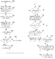
- Step 701 First, the edge edge acquisition rough pre-alignment is completed by using the edge vision acquisition system.
- Step 702 Calculate the notch direction, and calculate the angle of the rotating wafer according to the positional relationship between the notch, the mark, and the alignment mark field of view coordinates.
- Step 703 The R axis (ie, the axis of rotation in the vertical Z direction) is rotated to rotate the notch to the alignment field of view.
- Step 704 The motion component searches for the first mark according to the pre-aligned given mark position, and moves radially to the center of the wafer, and the maximum effective stroke is 75 mm.
- Step 705 The CCD camera captures an image and performs auto focus.
- Step 706 Determine whether the best focal plane is reached, and if yes, proceed to step 708: the first alignment mark image is acquired by the mark collection visual component, and if not, proceed to step 707: the focus adjustment component moves vertically, and proceeds to step 705 again.
- Step 709 Confirm whether there is already an alignment mark (in this case, the first alignment mark) in the image collected in step 708, and if found, proceed to step 714: determine whether both alignment marks have been found, if step 709 If no alignment mark is found, proceed to step 710: the R axis rotates clockwise or counterclockwise, each time the maximum rotation angle is 1.5 degrees, and the alignment mark is again collected by the mark acquisition visual component (in this case, the first alignment mark) Image.
- Step 711 It is determined again whether the alignment mark has been found. If it has been found, the process proceeds to step 714.
- step 712 the moving component moves +1 mm along the positive and negative limit positions, and then proceeds to step 709 again.
- step 713 the wafer is rotated 180 degrees around the R axis, and the mark is collected by the mark. The component captures the image of the second alignment mark and returns to step 709.
- step 715 calculate the positional deviation of the wafer from the workpiece stage based on the coordinates of the first and second alignment marks, and return the R angle value to the pre-pair
- the quasi-system returns the coordinate values of the first and second alignment marks in the wafer coordinate system (GWCS) to the workpiece stage, wherein the R angle is in the wafer coordinate system, the coordinate origin to the two alignment marks
- the angle of the line, the GWCS coordinate system is defined as: the origin of the coordinate is at the center of the wafer, the Y axis passes through the center of the trimming/grooving and the center of the wafer, and the X axis passes through the center of the wafer perpendicular to the Y axis.
- Step 716 Performing a higher precision pre-alignment on the wafer.
- the alignment mark is searched for in the above step 704, the measured value of the eccentricity of the wafer during the coarse pre-alignment and the theoretical position of the alignment mark in the wafer coordinate system (the position is determined once the mark setting is completed) can be positioned. Align the coordinates of the mark so that the alignment mark can be quickly found.
- the two marks MARK1 and MARK2 on the wafer are placed symmetrically, so the mark detection system will not need to search the MARK1 and MARK2 step by step along the R axis, as shown in FIG.
- W1 and W2 respectively represent two marks MARK1 and MARK2 symmetrically distributed on a wafer;
- N is an alignment mark coordinate The coordinate origin of the system (WCS coordinate system), where the WCS coordinate system is defined by the alignment mark, the midpoint of the line connecting the two marks is the coordinate origin, the Y coordinate axis passes the coordinate origin and is perpendicular to the line, and the wafer is trimmed.
- the U axis is defined as the line connecting the center of the workpiece stage and the center of the mark detection system.
- the V axis is defined as a line perpendicular to the U axis and passing through the center of the workpiece stage;
- W2' is MARK2 about O The position after the 180 degree rotation;
- the ⁇ (alfa) angle is the rotation angle between the WCS coordinate system and the MSCS coordinate system;
- P is the marker detection field of view The center of the range; the distance of NO is equal to W1M or MW2'.
- Y(W1) is the Y coordinate value of the alignment mark W1 in the MSCS coordinate system
- Y(W2') is the Y coordinate value after the alignment mark W2 is rotated by 180 degrees in the MSCS coordinate system.
- the value of the ⁇ angle is fed back to the workpiece table system, and the position of the wafer relative to the workpiece table is accurately compensated by the centering component and the orientation component of the workpiece table system, since the workpiece table system is opposite to the wafer Compensation for the position of the workpiece stage is known to those skilled in the art and will not be described herein.
- the origin O of the WSCS coordinate system is the center of the workpiece stage, and the relationship between the origin N of the WCS coordinate system (ie, the midpoint of the two marked lines) and the center of the wafer can be predetermined (when When the two marks are strictly symmetrically arranged about the center of the wafer, the N point is the center of the wafer; when the two marks are not symmetrically arranged about the center of the wafer, it is easy to calculate the offset between the point N and the center of the wafer.
- the two alignment marks W1 and W2 on the wafer are not symmetrically placed, but the lines of the two alignment marks W1 and W2 pass through the center of the wafer, and the two alignment marks W1 and W2 are wafer-to-wafer.
- the length of the connection to the center is inconsistent.
- the difference from the second embodiment is that after the first alignment mark W1 is found, the mark detecting system needs to rotate in the R-axis direction to find the second alignment mark W2.
- the fourth embodiment is based on the third embodiment, adding conditions that not only the two alignment marks W1 and W2 on the wafer are not symmetrically placed, but also the wafer has a relatively large eccentricity on the rotating table, that is, the wafer center Not in the center of the turntable, and the eccentricity is large.
- the mark detection system after the first alignment mark W1 is found, the mark detection system always rotates in the R-axis direction to find the second alignment mark W2. Then it is similar to the second embodiment. The only difference is the alignment mark with the GWCS coordinate system.
- the measurement position of W2 and the desired position of the alignment mark W2 in the WCS coordinate system are used to position the actual position of the alignment mark W2.
- the positions of the two alignment marks W1 and W2 on the wafer have different angles, and the lines of the two alignment marks W1 and W2 do not pass through the center of the wafer, while the two alignment marks W1
- the length of the connection from W2 to the center of the wafer is inconsistent. In fact, this situation is essentially the same as the fourth embodiment, and will not be described here.
- the relative positional relationship of the MSCS, GWCS, and WCS coordinate systems can be determined, thereby achieving fine alignment by position compensation for coarse alignment.
- the offset of the wafer on the rotating table is not too different from the marking position, so the fine alignment can be achieved after the second and third embodiments.
- the fourth and fifth embodiments only Used in rare cases to ensure precise alignment for all wafers.
Landscapes
- Engineering & Computer Science (AREA)
- Computer Vision & Pattern Recognition (AREA)
- Physics & Mathematics (AREA)
- General Physics & Mathematics (AREA)
- Theoretical Computer Science (AREA)
- Quality & Reliability (AREA)
- Container, Conveyance, Adherence, Positioning, Of Wafer (AREA)
- Exposure And Positioning Against Photoresist Photosensitive Materials (AREA)
Abstract
Description
Claims (9)
- 一种用于晶圆的预对准装置,其特征在于,包括:一工件台,用于承载所述晶圆,其中,所述晶圆上具有大致关于晶圆圆心对称分布的第一对准标记和第二对准标记;一边缘视觉采集系统,用于根据所述晶圆上的边缘或缺口标记关于工件台的相对位置,实现对所述晶圆的第一次位置补偿;一标记探测系统,用于分别获取所述第一和第二对准标记的像,并根据所述第一和第二对准标记在标记探测系统坐标系中的位置,确定所述晶圆圆心与工件台中心之间的相对位置关系,从而实现对所述晶圆的第二次位置补偿,其中,标记探测系统坐标系的横轴定义为工件台中心和标记探测系统中心的连线,纵轴定义为垂直于横轴并通过工件台中心的直线。
- 如权利要求1所述的用于晶圆的预对准装置,其特征在于,所述标记探测系统用于根据所述第一和第二对准标记在标记探测系统坐标系下的坐标计算出对准标记坐标系与标记探测系统坐标系之间的旋转角度及偏置,再根据所述旋转角度及偏置以及对准标记坐标系的原点与晶圆圆心之间的相对位置关系确定所述晶圆圆心与工件台中心之间的相对位置关系,其中,所述对准标记坐标系的横轴定义为所述第一和第二对准标记的连线,原点定义为所述第一和第二对准标记的连线的中点,纵轴经过原点且垂直于所述连线。
- 如权利要求1所述的用于晶圆的预对准装置,其特征在于,所述边缘视觉采集系统包括一线阵CCD探测器,所述标记探测系统包括一面阵CCD探测器。
- 如权利要求1所述的用于晶圆的预对准装置,其特征在于,所述标记探测系统包括一运动组件、一调焦组件以及一标记采集视觉组件,所述运动组件驱动所述标记采集视觉组件搜索所述第一或第二对准标记,所述调焦组 件用于调整标记采集视觉组件相对于第一或第二对准标记的焦距,所述标记采集视觉组件用于采集所述第一或第二对准标记的像。
- 如权利要求4所述的用于晶圆的预对准装置,其特征在于,所述调焦组件与所述运动组件相连接,所述标记采集视觉组件与所述调焦组件相连接,所述运动组件用于驱动所述调焦组件沿晶圆的径向移动,所述调焦组件用于驱动所述标记采集视觉组件沿竖直方向移动。
- 如权利要求4所述的用于晶圆的预对准装置,其特征在于,所述标记采集视觉组件包括一点光源、一镜头以及一面阵CCD相机。
- 如权利要求1所述的用于晶圆的预对准装置,其特征在于,所述边缘视觉采集系统和所述标记探测系统分别沿所述晶圆的径向位于所述晶圆的两侧。
- 一种用于晶圆的预对准方法,其特征在于,包括:步骤一、在晶圆上提供大致关于晶圆圆心对称分布的第一对准标记和第二对准标记;步骤二、由边缘视觉采集系统根据所述晶圆上的边缘或缺口标记关于工件台的相对位置,实现对所述晶圆的第一次位置补偿;步骤三、由标记探测系统分别搜索并采集位于所述晶圆上的第一、第二对准标记的像;步骤四、根据所述第一和第二对准标记在标记探测系统坐标系中的位置,确定所述晶圆圆心与工件台中心之间的相对位置关系;步骤五、根据所确定的所述晶圆圆心与工件台中心之间的相对位置关系,实现对所述晶圆的第二次位置补偿,其中,标记探测系统坐标系的横轴定义为工件台中心和标记探测系统中心的连线,纵轴定义为垂直于横轴并通过工件台中心的直线。
- 如权利要求8所述的用于晶圆的预对准方法,其特征在于,步骤四包括根据所述第一和第二对准标记在标记探测系统坐标系下的坐标计算出对准 标记坐标系与标记探测系统坐标系之间的旋转角度及偏置,再根据所述旋转角度及偏置以及对准标记坐标系的原点与晶圆圆心之间的相对位置关系确定所述晶圆圆心与工件台中心之间的相对位置关系,其中,所述对准标记坐标系的横轴定义为所述第一和第二对准标记的连线,原点定义为所述第一和第二对准标记的连线的中点,纵轴经过原点且垂直于所述连线。
Priority Applications (5)
| Application Number | Priority Date | Filing Date | Title |
|---|---|---|---|
| EP16782658.5A EP3288063B1 (en) | 2015-04-24 | 2016-04-22 | Pre-alignment device and method for wafer |
| KR1020177033877A KR102048301B1 (ko) | 2015-04-24 | 2016-04-22 | 웨이퍼를 위한 사전 정렬 장치 및 방법 |
| JP2017555261A JP6530825B2 (ja) | 2015-04-24 | 2016-04-22 | ウエハのプリアライメント装置及び方法 |
| SG11201708695PA SG11201708695PA (en) | 2015-04-24 | 2016-04-22 | Pre-alignment device and method for wafer |
| US15/568,657 US10276417B2 (en) | 2015-04-24 | 2016-04-22 | Pre-alignment device and method for wafer |
Applications Claiming Priority (2)
| Application Number | Priority Date | Filing Date | Title |
|---|---|---|---|
| CN201510203515.6 | 2015-04-24 | ||
| CN201510203515.6A CN106158715B (zh) | 2015-04-24 | 2015-04-24 | 用于晶圆的预对准装置及方法 |
Publications (1)
| Publication Number | Publication Date |
|---|---|
| WO2016169511A1 true WO2016169511A1 (zh) | 2016-10-27 |
Family
ID=57144391
Family Applications (1)
| Application Number | Title | Priority Date | Filing Date |
|---|---|---|---|
| PCT/CN2016/079979 Ceased WO2016169511A1 (zh) | 2015-04-24 | 2016-04-22 | 用于晶圆的预对准装置及方法 |
Country Status (8)
| Country | Link |
|---|---|
| US (1) | US10276417B2 (zh) |
| EP (1) | EP3288063B1 (zh) |
| JP (1) | JP6530825B2 (zh) |
| KR (1) | KR102048301B1 (zh) |
| CN (1) | CN106158715B (zh) |
| SG (1) | SG11201708695PA (zh) |
| TW (1) | TW201715638A (zh) |
| WO (1) | WO2016169511A1 (zh) |
Cited By (1)
| Publication number | Priority date | Publication date | Assignee | Title |
|---|---|---|---|---|
| CN114664721A (zh) * | 2022-03-21 | 2022-06-24 | 北京半导体专用设备研究所(中国电子科技集团公司第四十五研究所) | 一种晶圆位置预对准方法、电子设备及晶圆传输系统 |
Families Citing this family (35)
| Publication number | Priority date | Publication date | Assignee | Title |
|---|---|---|---|---|
| JP6423678B2 (ja) * | 2014-10-07 | 2018-11-14 | 東京エレクトロン株式会社 | 基板検査装置及びその制御方法 |
| CN105182702B (zh) * | 2015-10-30 | 2017-08-11 | 京东方科技集团股份有限公司 | 对位标记搜寻方法、显示基板和显示装置 |
| US10522326B2 (en) * | 2017-02-14 | 2019-12-31 | Massachusetts Institute Of Technology | Systems and methods for automated microscopy |
| CN108735644A (zh) * | 2017-04-25 | 2018-11-02 | 北京中科信电子装备有限公司 | 一种硅片定向及位置补偿的方法 |
| CN109451763B (zh) | 2018-05-16 | 2019-11-08 | 长江存储科技有限责任公司 | 用于晶圆键合对准补偿的方法和系统 |
| CN108615699B (zh) * | 2018-05-29 | 2023-11-07 | 深圳信息职业技术学院 | 一种晶圆对准系统及方法和用于晶圆对准的光学成像装置 |
| CN110488751B (zh) * | 2018-08-29 | 2022-08-19 | 中山大学 | 一种自动化工艺线的石墨料盘视觉定位系统 |
| WO2020083612A1 (en) | 2018-10-23 | 2020-04-30 | Asml Netherlands B.V. | Method and apparatus for adaptive alignment |
| CN109540904A (zh) * | 2018-12-12 | 2019-03-29 | 华侨大学 | 一种衬底表面宏观缺陷检测及分类系统 |
| WO2020181482A1 (en) * | 2019-03-12 | 2020-09-17 | Texas Instruments Incorporated | Method to improve nikon wafer loader repeatability |
| US11352698B2 (en) * | 2019-04-25 | 2022-06-07 | Samsung Electronics Co., Ltd. | Atomic layer deposition apparatus and methods of fabricating semiconductor devices using the same |
| CN110224052B (zh) * | 2019-05-28 | 2024-02-06 | 深圳新益昌科技股份有限公司 | 一种led固晶的双摆臂固晶装置及其固晶方法 |
| CN110729216A (zh) * | 2019-10-21 | 2020-01-24 | 华虹半导体(无锡)有限公司 | 晶圆位置检测装置、晶圆位置检测方法 |
| WO2021095553A1 (ja) | 2019-11-13 | 2021-05-20 | 株式会社エム・シー・ケー | 搬送装置及び搬送方法 |
| CN113066746B (zh) * | 2020-01-02 | 2022-03-22 | 长鑫存储技术有限公司 | 预对准装置及应用于该装置的预对准方法 |
| US12027400B2 (en) * | 2020-05-26 | 2024-07-02 | Asm Ip Holding B.V. | Automatic system calibration for wafer handling |
| CN111952230B (zh) * | 2020-09-01 | 2021-03-16 | 无锡卓海科技有限公司 | 一种预对准机的透明晶圆边缘提取方法 |
| CN114695225A (zh) * | 2020-12-31 | 2022-07-01 | 上海微电子装备(集团)股份有限公司 | 一种晶圆预对准装置和晶圆预对准方法 |
| CN112838038B (zh) * | 2021-02-02 | 2024-05-28 | 沈阳芯源微电子设备股份有限公司 | 对准方法及对准系统 |
| US11978677B2 (en) * | 2021-06-24 | 2024-05-07 | Taiwan Semiconductor Manufacturing Co., Ltd. | Wafer positioning method and apparatus |
| CN113251929B (zh) * | 2021-06-28 | 2021-10-29 | 深圳中科飞测科技股份有限公司 | 检测设备及检测方法、检测系统及存储介质 |
| CN114464564B (zh) * | 2022-01-18 | 2026-03-13 | 北京华卓精科科技股份有限公司 | 一种晶圆对准方法及装置 |
| CN116504666A (zh) * | 2022-01-19 | 2023-07-28 | 上海凯世通半导体股份有限公司 | 半导体晶圆位置检测装置、检测方法以及检测系统 |
| JP7830970B2 (ja) * | 2022-02-02 | 2026-03-17 | オムロン株式会社 | ずれ量の測定方法、及び測定装置、及びプログラム |
| CN114474440B (zh) * | 2022-03-16 | 2023-03-10 | 江苏京创先进电子科技有限公司 | 微调装置调整精度控制方法 |
| CN114823454B (zh) * | 2022-05-16 | 2026-01-23 | 北京华卓精科科技股份有限公司 | 一种晶圆对准装置及对准方法 |
| US20260050227A1 (en) * | 2022-09-20 | 2026-02-19 | Applied Materials, Inc. | On tool metrology scheme for advanced packaging |
| CN115831845A (zh) * | 2022-12-21 | 2023-03-21 | 绍兴中芯集成电路制造股份有限公司 | 晶圆预对准装置及晶圆预对准方法 |
| CN116422543B (zh) * | 2023-06-15 | 2023-09-08 | 苏州希盟科技股份有限公司 | 一种基于空间平面的点胶控制方法、装置、设备及介质 |
| CN116995011B (zh) * | 2023-08-16 | 2024-01-09 | 泓浒(苏州)半导体科技有限公司 | 一种用于晶圆载体装卸的校准方法和校准系统 |
| TWI846579B (zh) * | 2023-08-29 | 2024-06-21 | 三和技研股份有限公司 | 晶圓定位裝置與方法 |
| CN116878386B (zh) * | 2023-09-06 | 2023-12-08 | 北京华卓精科科技股份有限公司 | 上下对准视觉装置的标定方法及标定装置 |
| CN117012689B (zh) * | 2023-09-26 | 2023-12-15 | 天津中科晶禾电子科技有限责任公司 | 一种晶圆对准装置及方法 |
| CN118983255B (zh) * | 2024-08-06 | 2025-10-24 | 三河建华高科有限责任公司 | 一种高精度晶圆预对准机构 |
| CN119890118B (zh) * | 2024-12-27 | 2025-10-31 | 广东华矽半导体设备有限公司 | 一种基于视觉的晶圆预对准系统和方法 |
Citations (6)
| Publication number | Priority date | Publication date | Assignee | Title |
|---|---|---|---|---|
| US20080019817A1 (en) * | 2004-11-30 | 2008-01-24 | Kabushiki Kaisha Yaskawa Denki | Alignment Apparatus |
| US20080029715A1 (en) * | 2006-08-02 | 2008-02-07 | Disco Corporation | Alignment method of a laser beam processing machine |
| CN101128928A (zh) * | 2005-02-22 | 2008-02-20 | Oc欧瑞康巴尔斯公司 | 晶片的定位方法 |
| CN101216686A (zh) * | 2008-01-10 | 2008-07-09 | 上海微电子装备有限公司 | 一种晶片预对准平台及使用该平台的晶片预对准方法 |
| CN104364892A (zh) * | 2012-06-06 | 2015-02-18 | Ev集团E·索尔纳有限责任公司 | 用于确定对准误差的装置和方法 |
| TW201513259A (zh) * | 2013-06-17 | 2015-04-01 | Ev集團E塔那有限公司 | 用於基板對準之裝置及方法 |
Family Cites Families (26)
| Publication number | Priority date | Publication date | Assignee | Title |
|---|---|---|---|---|
| US3930684A (en) * | 1971-06-22 | 1976-01-06 | Lasch Jr Cecil A | Automatic wafer feeding and pre-alignment apparatus and method |
| US4376581A (en) * | 1979-12-20 | 1983-03-15 | Censor Patent- Und Versuchs-Anstalt | Method of positioning disk-shaped workpieces, preferably semiconductor wafers |
| US4461567A (en) * | 1979-12-20 | 1984-07-24 | Censor Patent- Und Versuchs-Anstalt | Method of and apparatus for the positioning of disk-shaped workpieces, particularly semiconductor wafers |
| JP2675307B2 (ja) * | 1987-08-28 | 1997-11-12 | 株式会社日立製作所 | プリアライナー装置 |
| US5044752A (en) * | 1989-06-30 | 1991-09-03 | General Signal Corporation | Apparatus and process for positioning wafers in receiving devices |
| JP2949528B2 (ja) * | 1991-03-13 | 1999-09-13 | 東京エレクトロン株式会社 | ウエハの中心位置検出方法及びその装置 |
| JP2000228347A (ja) * | 1999-02-08 | 2000-08-15 | Nikon Corp | 位置決め方法及び露光装置 |
| US6624433B2 (en) * | 1994-02-22 | 2003-09-23 | Nikon Corporation | Method and apparatus for positioning substrate and the like |
| US5563798A (en) * | 1994-04-05 | 1996-10-08 | Applied Materials, Inc. | Wafer positioning system |
| JP2000035676A (ja) * | 1998-05-15 | 2000-02-02 | Nippon Seiko Kk | 分割逐次近接露光装置 |
| US6237393B1 (en) * | 1999-07-30 | 2001-05-29 | International Business Machines Corporation | Wafer center alignment device and method of wafer alignment |
| US7008802B2 (en) * | 2001-05-29 | 2006-03-07 | Asm America, Inc. | Method and apparatus to correct water drift |
| JP2002365809A (ja) * | 2001-06-12 | 2002-12-18 | Nsk Ltd | 分割逐次露光装置 |
| TW594431B (en) * | 2002-03-01 | 2004-06-21 | Asml Netherlands Bv | Calibration methods, calibration substrates, lithographic apparatus and device manufacturing methods |
| US20040144760A1 (en) * | 2002-05-17 | 2004-07-29 | Cahill Steven P. | Method and system for marking a workpiece such as a semiconductor wafer and laser marker for use therein |
| JP2004281983A (ja) * | 2003-03-19 | 2004-10-07 | Toray Ind Inc | 位置決め装置および位置決め方法並びに塗布装置および塗布方法 |
| JP5239220B2 (ja) * | 2007-06-12 | 2013-07-17 | 株式会社ニコン | ウェハ位置決め装置と、これを有するウェハ貼り合わせ装置 |
| WO2010047378A1 (ja) * | 2008-10-24 | 2010-04-29 | 株式会社 日立ハイテクノロジーズ | 荷電粒子線装置 |
| JP2011021999A (ja) * | 2009-07-15 | 2011-02-03 | Kyodo Design & Planning Corp | 基板検査装置 |
| JP5524550B2 (ja) * | 2009-09-15 | 2014-06-18 | 株式会社ニコン | 基板接合装置、基板接合方法およびデバイスの製造方法 |
| JP2013026383A (ja) * | 2011-07-20 | 2013-02-04 | Dainippon Screen Mfg Co Ltd | 位置合わせ装置、位置合わせ方法、および、描画装置 |
| JP5836223B2 (ja) * | 2011-12-02 | 2015-12-24 | 株式会社神戸製鋼所 | 貼合基板の回転ズレ量計測装置、貼合基板の回転ズレ量計測方法、及び貼合基板の製造方法 |
| CN202661393U (zh) * | 2012-03-12 | 2013-01-09 | 苏州爱特盟光电有限公司 | 集成电路微观尺寸纳微检测仪 |
| JP5516684B2 (ja) | 2012-10-02 | 2014-06-11 | 株式会社ニコン | ウェハ貼り合わせ方法、位置決め方法と、これを有する半導体製造装置 |
| CN103604815B (zh) * | 2013-11-26 | 2016-01-13 | 上海海事大学 | 玻璃晶片检测装置与标定方法 |
| CN104536186B (zh) * | 2015-01-13 | 2017-12-08 | 合肥鑫晟光电科技有限公司 | 一种识别装置和对位系统 |
-
2015
- 2015-04-24 CN CN201510203515.6A patent/CN106158715B/zh active Active
-
2016
- 2016-04-22 EP EP16782658.5A patent/EP3288063B1/en active Active
- 2016-04-22 KR KR1020177033877A patent/KR102048301B1/ko active Active
- 2016-04-22 TW TW105112591A patent/TW201715638A/zh unknown
- 2016-04-22 US US15/568,657 patent/US10276417B2/en active Active
- 2016-04-22 SG SG11201708695PA patent/SG11201708695PA/en unknown
- 2016-04-22 WO PCT/CN2016/079979 patent/WO2016169511A1/zh not_active Ceased
- 2016-04-22 JP JP2017555261A patent/JP6530825B2/ja active Active
Patent Citations (6)
| Publication number | Priority date | Publication date | Assignee | Title |
|---|---|---|---|---|
| US20080019817A1 (en) * | 2004-11-30 | 2008-01-24 | Kabushiki Kaisha Yaskawa Denki | Alignment Apparatus |
| CN101128928A (zh) * | 2005-02-22 | 2008-02-20 | Oc欧瑞康巴尔斯公司 | 晶片的定位方法 |
| US20080029715A1 (en) * | 2006-08-02 | 2008-02-07 | Disco Corporation | Alignment method of a laser beam processing machine |
| CN101216686A (zh) * | 2008-01-10 | 2008-07-09 | 上海微电子装备有限公司 | 一种晶片预对准平台及使用该平台的晶片预对准方法 |
| CN104364892A (zh) * | 2012-06-06 | 2015-02-18 | Ev集团E·索尔纳有限责任公司 | 用于确定对准误差的装置和方法 |
| TW201513259A (zh) * | 2013-06-17 | 2015-04-01 | Ev集團E塔那有限公司 | 用於基板對準之裝置及方法 |
Non-Patent Citations (1)
| Title |
|---|
| See also references of EP3288063A4 * |
Cited By (2)
| Publication number | Priority date | Publication date | Assignee | Title |
|---|---|---|---|---|
| CN114664721A (zh) * | 2022-03-21 | 2022-06-24 | 北京半导体专用设备研究所(中国电子科技集团公司第四十五研究所) | 一种晶圆位置预对准方法、电子设备及晶圆传输系统 |
| CN114664721B (zh) * | 2022-03-21 | 2025-12-05 | 北京半导体专用设备研究所(中国电子科技集团公司第四十五研究所) | 一种晶圆位置预对准方法、电子设备及晶圆传输系统 |
Also Published As
| Publication number | Publication date |
|---|---|
| US20180151400A1 (en) | 2018-05-31 |
| US10276417B2 (en) | 2019-04-30 |
| EP3288063B1 (en) | 2020-02-26 |
| KR20170137927A (ko) | 2017-12-13 |
| KR102048301B1 (ko) | 2019-11-25 |
| EP3288063A1 (en) | 2018-02-28 |
| JP2018513563A (ja) | 2018-05-24 |
| SG11201708695PA (en) | 2017-11-29 |
| EP3288063A4 (en) | 2018-12-05 |
| CN106158715B (zh) | 2021-04-02 |
| TW201715638A (zh) | 2017-05-01 |
| CN106158715A (zh) | 2016-11-23 |
| JP6530825B2 (ja) | 2019-06-12 |
Similar Documents
| Publication | Publication Date | Title |
|---|---|---|
| WO2016169511A1 (zh) | 用于晶圆的预对准装置及方法 | |
| CN110006905B (zh) | 一种线面阵相机结合的大口径超净光滑表面缺陷检测装置 | |
| CN114695225A (zh) | 一种晶圆预对准装置和晶圆预对准方法 | |
| CN107957626B (zh) | 一种面向光学镜片的六自由度并联自动调偏系统及方法 | |
| US20140290047A1 (en) | Workpiece mounting apparatus | |
| CN108332946B (zh) | 一种微透镜阵列模具车削加工中的反射焦距在位检测方法 | |
| JP2004288792A (ja) | アライメント装置及びアライメント方法 | |
| CN105352449A (zh) | 一种机器视觉零件外形、外廓尺寸测量系统及测量检验方法 | |
| CN115031626B (zh) | 一种基片坐标测量方法 | |
| CN104111595A (zh) | 用于光刻设备的预对准装置及方法 | |
| KR102838138B1 (ko) | 웨이퍼 접합 장치 | |
| CN115128914B (zh) | 一种应用于全场曝光机的调平对位方法 | |
| CN104154885A (zh) | 一种小圆环零件微翘曲检测方法 | |
| CN103681426B (zh) | 大翘曲硅片预对准装置及方法 | |
| CN102280400A (zh) | 一种激光束加工处理中的晶圆片对准方法 | |
| CN113639633B (zh) | 一种多轴视觉测量装置中夹具角向零位找正方法 | |
| CN119108317B (zh) | 晶圆寻边方法和装置 | |
| CN120280383B (zh) | 晶圆寻边扫码方法及装置 | |
| CN111288933B (zh) | 一种球面或旋转对称非球面光学元件自动定心方法 | |
| CN104678720A (zh) | 利用掩模对准系统进行工件台基准板旋转探测的方法 | |
| KR102065190B1 (ko) | 경질 취성판의 연삭장치와 가공 정밀도의 계측 및 보정 방법 | |
| CN111550480A (zh) | 一种空间精密位姿对准方法 | |
| CN118824881A (zh) | 一种套刻误差量测装置和量测方法 | |
| CN114111578A (zh) | 一种大口径元件的位姿自动确定方法 | |
| CN103246166B (zh) | 一种硅片预对准测量装置 |
Legal Events
| Date | Code | Title | Description |
|---|---|---|---|
| 121 | Ep: the epo has been informed by wipo that ep was designated in this application |
Ref document number: 16782658 Country of ref document: EP Kind code of ref document: A1 |
|
| ENP | Entry into the national phase |
Ref document number: 2017555261 Country of ref document: JP Kind code of ref document: A |
|
| WWE | Wipo information: entry into national phase |
Ref document number: 15568657 Country of ref document: US |
|
| NENP | Non-entry into the national phase |
Ref country code: DE |
|
| ENP | Entry into the national phase |
Ref document number: 20177033877 Country of ref document: KR Kind code of ref document: A |
|
| WWE | Wipo information: entry into national phase |
Ref document number: 2016782658 Country of ref document: EP |