WO2016181965A1 - 電気音響変換フィルム原反、電気音響変換フィルム、および、その製造方法 - Google Patents
電気音響変換フィルム原反、電気音響変換フィルム、および、その製造方法 Download PDFInfo
- Publication number
- WO2016181965A1 WO2016181965A1 PCT/JP2016/063883 JP2016063883W WO2016181965A1 WO 2016181965 A1 WO2016181965 A1 WO 2016181965A1 JP 2016063883 W JP2016063883 W JP 2016063883W WO 2016181965 A1 WO2016181965 A1 WO 2016181965A1
- Authority
- WO
- WIPO (PCT)
- Prior art keywords
- electrode
- piezoelectric layer
- thin film
- conversion film
- piezoelectric
- Prior art date
- Legal status (The legal status is an assumption and is not a legal conclusion. Google has not performed a legal analysis and makes no representation as to the accuracy of the status listed.)
- Ceased
Links
Images


Classifications
-
- B—PERFORMING OPERATIONS; TRANSPORTING
- B32—LAYERED PRODUCTS
- B32B—LAYERED PRODUCTS, i.e. PRODUCTS BUILT-UP OF STRATA OF FLAT OR NON-FLAT, e.g. CELLULAR OR HONEYCOMB, FORM
- B32B3/00—Layered products comprising a layer with external or internal discontinuities or unevennesses, or a layer of non-planar shape; Layered products comprising a layer having particular features of form
- B32B3/02—Layered products comprising a layer with external or internal discontinuities or unevennesses, or a layer of non-planar shape; Layered products comprising a layer having particular features of form characterised by features of form at particular places, e.g. in edge regions
- B32B3/04—Layered products comprising a layer with external or internal discontinuities or unevennesses, or a layer of non-planar shape; Layered products comprising a layer having particular features of form characterised by features of form at particular places, e.g. in edge regions characterised by at least one layer folded at the edge, e.g. over another layer ; characterised by at least one layer enveloping or enclosing a material
-
- H—ELECTRICITY
- H10—SEMICONDUCTOR DEVICES; ELECTRIC SOLID-STATE DEVICES NOT OTHERWISE PROVIDED FOR
- H10N—ELECTRIC SOLID-STATE DEVICES NOT OTHERWISE PROVIDED FOR
- H10N30/00—Piezoelectric or electrostrictive devices
- H10N30/01—Manufacture or treatment
- H10N30/07—Forming of piezoelectric or electrostrictive parts or bodies on an electrical element or another base
- H10N30/072—Forming of piezoelectric or electrostrictive parts or bodies on an electrical element or another base by laminating or bonding of piezoelectric or electrostrictive bodies
-
- B—PERFORMING OPERATIONS; TRANSPORTING
- B32—LAYERED PRODUCTS
- B32B—LAYERED PRODUCTS, i.e. PRODUCTS BUILT-UP OF STRATA OF FLAT OR NON-FLAT, e.g. CELLULAR OR HONEYCOMB, FORM
- B32B23/00—Layered products comprising a layer of cellulosic plastic substances, i.e. substances obtained by chemical modification of cellulose, e.g. cellulose ethers, cellulose esters, viscose
- B32B23/04—Layered products comprising a layer of cellulosic plastic substances, i.e. substances obtained by chemical modification of cellulose, e.g. cellulose ethers, cellulose esters, viscose comprising such cellulosic plastic substance as the main or only constituent of a layer, which is next to another layer of the same or of a different material
-
- B—PERFORMING OPERATIONS; TRANSPORTING
- B32—LAYERED PRODUCTS
- B32B—LAYERED PRODUCTS, i.e. PRODUCTS BUILT-UP OF STRATA OF FLAT OR NON-FLAT, e.g. CELLULAR OR HONEYCOMB, FORM
- B32B23/00—Layered products comprising a layer of cellulosic plastic substances, i.e. substances obtained by chemical modification of cellulose, e.g. cellulose ethers, cellulose esters, viscose
- B32B23/04—Layered products comprising a layer of cellulosic plastic substances, i.e. substances obtained by chemical modification of cellulose, e.g. cellulose ethers, cellulose esters, viscose comprising such cellulosic plastic substance as the main or only constituent of a layer, which is next to another layer of the same or of a different material
- B32B23/048—Layered products comprising a layer of cellulosic plastic substances, i.e. substances obtained by chemical modification of cellulose, e.g. cellulose ethers, cellulose esters, viscose comprising such cellulosic plastic substance as the main or only constituent of a layer, which is next to another layer of the same or of a different material of foam
-
- B—PERFORMING OPERATIONS; TRANSPORTING
- B32—LAYERED PRODUCTS
- B32B—LAYERED PRODUCTS, i.e. PRODUCTS BUILT-UP OF STRATA OF FLAT OR NON-FLAT, e.g. CELLULAR OR HONEYCOMB, FORM
- B32B23/00—Layered products comprising a layer of cellulosic plastic substances, i.e. substances obtained by chemical modification of cellulose, e.g. cellulose ethers, cellulose esters, viscose
- B32B23/04—Layered products comprising a layer of cellulosic plastic substances, i.e. substances obtained by chemical modification of cellulose, e.g. cellulose ethers, cellulose esters, viscose comprising such cellulosic plastic substance as the main or only constituent of a layer, which is next to another layer of the same or of a different material
- B32B23/08—Layered products comprising a layer of cellulosic plastic substances, i.e. substances obtained by chemical modification of cellulose, e.g. cellulose ethers, cellulose esters, viscose comprising such cellulosic plastic substance as the main or only constituent of a layer, which is next to another layer of the same or of a different material of synthetic resin
-
- B—PERFORMING OPERATIONS; TRANSPORTING
- B32—LAYERED PRODUCTS
- B32B—LAYERED PRODUCTS, i.e. PRODUCTS BUILT-UP OF STRATA OF FLAT OR NON-FLAT, e.g. CELLULAR OR HONEYCOMB, FORM
- B32B23/00—Layered products comprising a layer of cellulosic plastic substances, i.e. substances obtained by chemical modification of cellulose, e.g. cellulose ethers, cellulose esters, viscose
- B32B23/10—Layered products comprising a layer of cellulosic plastic substances, i.e. substances obtained by chemical modification of cellulose, e.g. cellulose ethers, cellulose esters, viscose next to a fibrous or filamentary layer
-
- B—PERFORMING OPERATIONS; TRANSPORTING
- B32—LAYERED PRODUCTS
- B32B—LAYERED PRODUCTS, i.e. PRODUCTS BUILT-UP OF STRATA OF FLAT OR NON-FLAT, e.g. CELLULAR OR HONEYCOMB, FORM
- B32B25/00—Layered products comprising a layer of natural or synthetic rubber
- B32B25/04—Layered products comprising a layer of natural or synthetic rubber comprising rubber as the main or only constituent of a layer, which is next to another layer of the same or of a different material
- B32B25/08—Layered products comprising a layer of natural or synthetic rubber comprising rubber as the main or only constituent of a layer, which is next to another layer of the same or of a different material of synthetic resin
-
- B—PERFORMING OPERATIONS; TRANSPORTING
- B32—LAYERED PRODUCTS
- B32B—LAYERED PRODUCTS, i.e. PRODUCTS BUILT-UP OF STRATA OF FLAT OR NON-FLAT, e.g. CELLULAR OR HONEYCOMB, FORM
- B32B25/00—Layered products comprising a layer of natural or synthetic rubber
- B32B25/12—Layered products comprising a layer of natural or synthetic rubber comprising natural rubber
-
- B—PERFORMING OPERATIONS; TRANSPORTING
- B32—LAYERED PRODUCTS
- B32B—LAYERED PRODUCTS, i.e. PRODUCTS BUILT-UP OF STRATA OF FLAT OR NON-FLAT, e.g. CELLULAR OR HONEYCOMB, FORM
- B32B25/00—Layered products comprising a layer of natural or synthetic rubber
- B32B25/14—Layered products comprising a layer of natural or synthetic rubber comprising synthetic rubber copolymers
-
- B—PERFORMING OPERATIONS; TRANSPORTING
- B32—LAYERED PRODUCTS
- B32B—LAYERED PRODUCTS, i.e. PRODUCTS BUILT-UP OF STRATA OF FLAT OR NON-FLAT, e.g. CELLULAR OR HONEYCOMB, FORM
- B32B27/00—Layered products comprising a layer of synthetic resin
- B32B27/06—Layered products comprising a layer of synthetic resin as the main or only constituent of a layer, which is next to another layer of the same or of a different material
- B32B27/065—Layered products comprising a layer of synthetic resin as the main or only constituent of a layer, which is next to another layer of the same or of a different material of foam
-
- B—PERFORMING OPERATIONS; TRANSPORTING
- B32—LAYERED PRODUCTS
- B32B—LAYERED PRODUCTS, i.e. PRODUCTS BUILT-UP OF STRATA OF FLAT OR NON-FLAT, e.g. CELLULAR OR HONEYCOMB, FORM
- B32B27/00—Layered products comprising a layer of synthetic resin
- B32B27/06—Layered products comprising a layer of synthetic resin as the main or only constituent of a layer, which is next to another layer of the same or of a different material
- B32B27/08—Layered products comprising a layer of synthetic resin as the main or only constituent of a layer, which is next to another layer of the same or of a different material of synthetic resin
-
- B—PERFORMING OPERATIONS; TRANSPORTING
- B32—LAYERED PRODUCTS
- B32B—LAYERED PRODUCTS, i.e. PRODUCTS BUILT-UP OF STRATA OF FLAT OR NON-FLAT, e.g. CELLULAR OR HONEYCOMB, FORM
- B32B27/00—Layered products comprising a layer of synthetic resin
- B32B27/06—Layered products comprising a layer of synthetic resin as the main or only constituent of a layer, which is next to another layer of the same or of a different material
- B32B27/10—Layered products comprising a layer of synthetic resin as the main or only constituent of a layer, which is next to another layer of the same or of a different material of paper or cardboard
-
- B—PERFORMING OPERATIONS; TRANSPORTING
- B32—LAYERED PRODUCTS
- B32B—LAYERED PRODUCTS, i.e. PRODUCTS BUILT-UP OF STRATA OF FLAT OR NON-FLAT, e.g. CELLULAR OR HONEYCOMB, FORM
- B32B27/00—Layered products comprising a layer of synthetic resin
- B32B27/12—Layered products comprising a layer of synthetic resin next to a fibrous or filamentary layer
-
- B—PERFORMING OPERATIONS; TRANSPORTING
- B32—LAYERED PRODUCTS
- B32B—LAYERED PRODUCTS, i.e. PRODUCTS BUILT-UP OF STRATA OF FLAT OR NON-FLAT, e.g. CELLULAR OR HONEYCOMB, FORM
- B32B27/00—Layered products comprising a layer of synthetic resin
- B32B27/28—Layered products comprising a layer of synthetic resin comprising synthetic resins not wholly covered by any one of the sub-groups B32B27/30 - B32B27/42
- B32B27/281—Layered products comprising a layer of synthetic resin comprising synthetic resins not wholly covered by any one of the sub-groups B32B27/30 - B32B27/42 comprising polyimides
-
- B—PERFORMING OPERATIONS; TRANSPORTING
- B32—LAYERED PRODUCTS
- B32B—LAYERED PRODUCTS, i.e. PRODUCTS BUILT-UP OF STRATA OF FLAT OR NON-FLAT, e.g. CELLULAR OR HONEYCOMB, FORM
- B32B27/00—Layered products comprising a layer of synthetic resin
- B32B27/28—Layered products comprising a layer of synthetic resin comprising synthetic resins not wholly covered by any one of the sub-groups B32B27/30 - B32B27/42
- B32B27/285—Layered products comprising a layer of synthetic resin comprising synthetic resins not wholly covered by any one of the sub-groups B32B27/30 - B32B27/42 comprising polyethers
-
- B—PERFORMING OPERATIONS; TRANSPORTING
- B32—LAYERED PRODUCTS
- B32B—LAYERED PRODUCTS, i.e. PRODUCTS BUILT-UP OF STRATA OF FLAT OR NON-FLAT, e.g. CELLULAR OR HONEYCOMB, FORM
- B32B27/00—Layered products comprising a layer of synthetic resin
- B32B27/28—Layered products comprising a layer of synthetic resin comprising synthetic resins not wholly covered by any one of the sub-groups B32B27/30 - B32B27/42
- B32B27/286—Layered products comprising a layer of synthetic resin comprising synthetic resins not wholly covered by any one of the sub-groups B32B27/30 - B32B27/42 comprising polysulphones; polysulfides
-
- B—PERFORMING OPERATIONS; TRANSPORTING
- B32—LAYERED PRODUCTS
- B32B—LAYERED PRODUCTS, i.e. PRODUCTS BUILT-UP OF STRATA OF FLAT OR NON-FLAT, e.g. CELLULAR OR HONEYCOMB, FORM
- B32B27/00—Layered products comprising a layer of synthetic resin
- B32B27/30—Layered products comprising a layer of synthetic resin comprising vinyl (co)polymers; comprising acrylic (co)polymers
-
- B—PERFORMING OPERATIONS; TRANSPORTING
- B32—LAYERED PRODUCTS
- B32B—LAYERED PRODUCTS, i.e. PRODUCTS BUILT-UP OF STRATA OF FLAT OR NON-FLAT, e.g. CELLULAR OR HONEYCOMB, FORM
- B32B27/00—Layered products comprising a layer of synthetic resin
- B32B27/30—Layered products comprising a layer of synthetic resin comprising vinyl (co)polymers; comprising acrylic (co)polymers
- B32B27/302—Layered products comprising a layer of synthetic resin comprising vinyl (co)polymers; comprising acrylic (co)polymers comprising aromatic vinyl (co)polymers, e.g. styrenic (co)polymers
-
- B—PERFORMING OPERATIONS; TRANSPORTING
- B32—LAYERED PRODUCTS
- B32B—LAYERED PRODUCTS, i.e. PRODUCTS BUILT-UP OF STRATA OF FLAT OR NON-FLAT, e.g. CELLULAR OR HONEYCOMB, FORM
- B32B27/00—Layered products comprising a layer of synthetic resin
- B32B27/32—Layered products comprising a layer of synthetic resin comprising polyolefins
-
- B—PERFORMING OPERATIONS; TRANSPORTING
- B32—LAYERED PRODUCTS
- B32B—LAYERED PRODUCTS, i.e. PRODUCTS BUILT-UP OF STRATA OF FLAT OR NON-FLAT, e.g. CELLULAR OR HONEYCOMB, FORM
- B32B27/00—Layered products comprising a layer of synthetic resin
- B32B27/32—Layered products comprising a layer of synthetic resin comprising polyolefins
- B32B27/325—Layered products comprising a layer of synthetic resin comprising polyolefins comprising polycycloolefins
-
- B—PERFORMING OPERATIONS; TRANSPORTING
- B32—LAYERED PRODUCTS
- B32B—LAYERED PRODUCTS, i.e. PRODUCTS BUILT-UP OF STRATA OF FLAT OR NON-FLAT, e.g. CELLULAR OR HONEYCOMB, FORM
- B32B27/00—Layered products comprising a layer of synthetic resin
- B32B27/36—Layered products comprising a layer of synthetic resin comprising polyesters
-
- B—PERFORMING OPERATIONS; TRANSPORTING
- B32—LAYERED PRODUCTS
- B32B—LAYERED PRODUCTS, i.e. PRODUCTS BUILT-UP OF STRATA OF FLAT OR NON-FLAT, e.g. CELLULAR OR HONEYCOMB, FORM
- B32B27/00—Layered products comprising a layer of synthetic resin
- B32B27/36—Layered products comprising a layer of synthetic resin comprising polyesters
- B32B27/365—Layered products comprising a layer of synthetic resin comprising polyesters comprising polycarbonates
-
- B—PERFORMING OPERATIONS; TRANSPORTING
- B32—LAYERED PRODUCTS
- B32B—LAYERED PRODUCTS, i.e. PRODUCTS BUILT-UP OF STRATA OF FLAT OR NON-FLAT, e.g. CELLULAR OR HONEYCOMB, FORM
- B32B29/00—Layered products comprising a layer of paper or cardboard
- B32B29/002—Layered products comprising a layer of paper or cardboard as the main or only constituent of a layer, which is next to another layer of the same or of a different material
- B32B29/005—Layered products comprising a layer of paper or cardboard as the main or only constituent of a layer, which is next to another layer of the same or of a different material next to another layer of paper or cardboard layer
-
- B—PERFORMING OPERATIONS; TRANSPORTING
- B32—LAYERED PRODUCTS
- B32B—LAYERED PRODUCTS, i.e. PRODUCTS BUILT-UP OF STRATA OF FLAT OR NON-FLAT, e.g. CELLULAR OR HONEYCOMB, FORM
- B32B29/00—Layered products comprising a layer of paper or cardboard
- B32B29/002—Layered products comprising a layer of paper or cardboard as the main or only constituent of a layer, which is next to another layer of the same or of a different material
- B32B29/007—Layered products comprising a layer of paper or cardboard as the main or only constituent of a layer, which is next to another layer of the same or of a different material next to a foam layer
-
- B—PERFORMING OPERATIONS; TRANSPORTING
- B32—LAYERED PRODUCTS
- B32B—LAYERED PRODUCTS, i.e. PRODUCTS BUILT-UP OF STRATA OF FLAT OR NON-FLAT, e.g. CELLULAR OR HONEYCOMB, FORM
- B32B29/00—Layered products comprising a layer of paper or cardboard
- B32B29/02—Layered products comprising a layer of paper or cardboard next to a fibrous or filamentary layer
-
- B—PERFORMING OPERATIONS; TRANSPORTING
- B32—LAYERED PRODUCTS
- B32B—LAYERED PRODUCTS, i.e. PRODUCTS BUILT-UP OF STRATA OF FLAT OR NON-FLAT, e.g. CELLULAR OR HONEYCOMB, FORM
- B32B3/00—Layered products comprising a layer with external or internal discontinuities or unevennesses, or a layer of non-planar shape; Layered products comprising a layer having particular features of form
- B32B3/26—Layered products comprising a layer with external or internal discontinuities or unevennesses, or a layer of non-planar shape; Layered products comprising a layer having particular features of form characterised by a particular shape of the outline of the cross-section of a continuous layer; characterised by a layer with cavities or internal voids ; characterised by an apertured layer
- B32B3/30—Layered products comprising a layer with external or internal discontinuities or unevennesses, or a layer of non-planar shape; Layered products comprising a layer having particular features of form characterised by a particular shape of the outline of the cross-section of a continuous layer; characterised by a layer with cavities or internal voids ; characterised by an apertured layer characterised by a layer formed with recesses or projections, e.g. hollows, grooves, protuberances, ribs
-
- B—PERFORMING OPERATIONS; TRANSPORTING
- B32—LAYERED PRODUCTS
- B32B—LAYERED PRODUCTS, i.e. PRODUCTS BUILT-UP OF STRATA OF FLAT OR NON-FLAT, e.g. CELLULAR OR HONEYCOMB, FORM
- B32B37/00—Methods or apparatus for laminating, e.g. by curing or by ultrasonic bonding
- B32B37/12—Methods or apparatus for laminating, e.g. by curing or by ultrasonic bonding characterised by using adhesives
-
- B—PERFORMING OPERATIONS; TRANSPORTING
- B32—LAYERED PRODUCTS
- B32B—LAYERED PRODUCTS, i.e. PRODUCTS BUILT-UP OF STRATA OF FLAT OR NON-FLAT, e.g. CELLULAR OR HONEYCOMB, FORM
- B32B37/00—Methods or apparatus for laminating, e.g. by curing or by ultrasonic bonding
- B32B37/14—Methods or apparatus for laminating, e.g. by curing or by ultrasonic bonding characterised by the properties of the layers
-
- B—PERFORMING OPERATIONS; TRANSPORTING
- B32—LAYERED PRODUCTS
- B32B—LAYERED PRODUCTS, i.e. PRODUCTS BUILT-UP OF STRATA OF FLAT OR NON-FLAT, e.g. CELLULAR OR HONEYCOMB, FORM
- B32B38/00—Ancillary operations in connection with laminating processes
- B32B38/0004—Cutting, tearing or severing, e.g. bursting; Cutter details
-
- B—PERFORMING OPERATIONS; TRANSPORTING
- B32—LAYERED PRODUCTS
- B32B—LAYERED PRODUCTS, i.e. PRODUCTS BUILT-UP OF STRATA OF FLAT OR NON-FLAT, e.g. CELLULAR OR HONEYCOMB, FORM
- B32B5/00—Layered products characterised by the non- homogeneity or physical structure, i.e. comprising a fibrous, filamentary, particulate or foam layer; Layered products characterised by having a layer differing constitutionally or physically in different parts
- B32B5/02—Layered products characterised by the non- homogeneity or physical structure, i.e. comprising a fibrous, filamentary, particulate or foam layer; Layered products characterised by having a layer differing constitutionally or physically in different parts characterised by structural features of a fibrous or filamentary layer
- B32B5/022—Non-woven fabric
-
- B—PERFORMING OPERATIONS; TRANSPORTING
- B32—LAYERED PRODUCTS
- B32B—LAYERED PRODUCTS, i.e. PRODUCTS BUILT-UP OF STRATA OF FLAT OR NON-FLAT, e.g. CELLULAR OR HONEYCOMB, FORM
- B32B5/00—Layered products characterised by the non- homogeneity or physical structure, i.e. comprising a fibrous, filamentary, particulate or foam layer; Layered products characterised by having a layer differing constitutionally or physically in different parts
- B32B5/18—Layered products characterised by the non- homogeneity or physical structure, i.e. comprising a fibrous, filamentary, particulate or foam layer; Layered products characterised by having a layer differing constitutionally or physically in different parts characterised by features of a layer of foamed material
-
- B—PERFORMING OPERATIONS; TRANSPORTING
- B32—LAYERED PRODUCTS
- B32B—LAYERED PRODUCTS, i.e. PRODUCTS BUILT-UP OF STRATA OF FLAT OR NON-FLAT, e.g. CELLULAR OR HONEYCOMB, FORM
- B32B5/00—Layered products characterised by the non- homogeneity or physical structure, i.e. comprising a fibrous, filamentary, particulate or foam layer; Layered products characterised by having a layer differing constitutionally or physically in different parts
- B32B5/22—Layered products characterised by the non- homogeneity or physical structure, i.e. comprising a fibrous, filamentary, particulate or foam layer; Layered products characterised by having a layer differing constitutionally or physically in different parts characterised by the presence of two or more layers which are next to each other and are fibrous, filamentary, formed of particles or foamed
- B32B5/24—Layered products characterised by the non- homogeneity or physical structure, i.e. comprising a fibrous, filamentary, particulate or foam layer; Layered products characterised by having a layer differing constitutionally or physically in different parts characterised by the presence of two or more layers which are next to each other and are fibrous, filamentary, formed of particles or foamed one layer being a fibrous or filamentary layer
- B32B5/245—Layered products characterised by the non- homogeneity or physical structure, i.e. comprising a fibrous, filamentary, particulate or foam layer; Layered products characterised by having a layer differing constitutionally or physically in different parts characterised by the presence of two or more layers which are next to each other and are fibrous, filamentary, formed of particles or foamed one layer being a fibrous or filamentary layer another layer next to it being a foam layer
-
- B—PERFORMING OPERATIONS; TRANSPORTING
- B32—LAYERED PRODUCTS
- B32B—LAYERED PRODUCTS, i.e. PRODUCTS BUILT-UP OF STRATA OF FLAT OR NON-FLAT, e.g. CELLULAR OR HONEYCOMB, FORM
- B32B5/00—Layered products characterised by the non- homogeneity or physical structure, i.e. comprising a fibrous, filamentary, particulate or foam layer; Layered products characterised by having a layer differing constitutionally or physically in different parts
- B32B5/22—Layered products characterised by the non- homogeneity or physical structure, i.e. comprising a fibrous, filamentary, particulate or foam layer; Layered products characterised by having a layer differing constitutionally or physically in different parts characterised by the presence of two or more layers which are next to each other and are fibrous, filamentary, formed of particles or foamed
- B32B5/24—Layered products characterised by the non- homogeneity or physical structure, i.e. comprising a fibrous, filamentary, particulate or foam layer; Layered products characterised by having a layer differing constitutionally or physically in different parts characterised by the presence of two or more layers which are next to each other and are fibrous, filamentary, formed of particles or foamed one layer being a fibrous or filamentary layer
- B32B5/26—Layered products characterised by the non- homogeneity or physical structure, i.e. comprising a fibrous, filamentary, particulate or foam layer; Layered products characterised by having a layer differing constitutionally or physically in different parts characterised by the presence of two or more layers which are next to each other and are fibrous, filamentary, formed of particles or foamed one layer being a fibrous or filamentary layer another layer next to it also being fibrous or filamentary
-
- B—PERFORMING OPERATIONS; TRANSPORTING
- B32—LAYERED PRODUCTS
- B32B—LAYERED PRODUCTS, i.e. PRODUCTS BUILT-UP OF STRATA OF FLAT OR NON-FLAT, e.g. CELLULAR OR HONEYCOMB, FORM
- B32B5/00—Layered products characterised by the non- homogeneity or physical structure, i.e. comprising a fibrous, filamentary, particulate or foam layer; Layered products characterised by having a layer differing constitutionally or physically in different parts
- B32B5/22—Layered products characterised by the non- homogeneity or physical structure, i.e. comprising a fibrous, filamentary, particulate or foam layer; Layered products characterised by having a layer differing constitutionally or physically in different parts characterised by the presence of two or more layers which are next to each other and are fibrous, filamentary, formed of particles or foamed
- B32B5/32—Layered products characterised by the non- homogeneity or physical structure, i.e. comprising a fibrous, filamentary, particulate or foam layer; Layered products characterised by having a layer differing constitutionally or physically in different parts characterised by the presence of two or more layers which are next to each other and are fibrous, filamentary, formed of particles or foamed at least two layers being foamed and next to each other
-
- B—PERFORMING OPERATIONS; TRANSPORTING
- B32—LAYERED PRODUCTS
- B32B—LAYERED PRODUCTS, i.e. PRODUCTS BUILT-UP OF STRATA OF FLAT OR NON-FLAT, e.g. CELLULAR OR HONEYCOMB, FORM
- B32B7/00—Layered products characterised by the relation between layers; Layered products characterised by the relative orientation of features between layers, or by the relative values of a measurable parameter between layers, i.e. products comprising layers having different physical, chemical or physicochemical properties; Layered products characterised by the interconnection of layers
- B32B7/02—Physical, chemical or physicochemical properties
-
- B—PERFORMING OPERATIONS; TRANSPORTING
- B32—LAYERED PRODUCTS
- B32B—LAYERED PRODUCTS, i.e. PRODUCTS BUILT-UP OF STRATA OF FLAT OR NON-FLAT, e.g. CELLULAR OR HONEYCOMB, FORM
- B32B7/00—Layered products characterised by the relation between layers; Layered products characterised by the relative orientation of features between layers, or by the relative values of a measurable parameter between layers, i.e. products comprising layers having different physical, chemical or physicochemical properties; Layered products characterised by the interconnection of layers
- B32B7/04—Interconnection of layers
- B32B7/06—Interconnection of layers permitting easy separation
-
- B—PERFORMING OPERATIONS; TRANSPORTING
- B32—LAYERED PRODUCTS
- B32B—LAYERED PRODUCTS, i.e. PRODUCTS BUILT-UP OF STRATA OF FLAT OR NON-FLAT, e.g. CELLULAR OR HONEYCOMB, FORM
- B32B7/00—Layered products characterised by the relation between layers; Layered products characterised by the relative orientation of features between layers, or by the relative values of a measurable parameter between layers, i.e. products comprising layers having different physical, chemical or physicochemical properties; Layered products characterised by the interconnection of layers
- B32B7/04—Interconnection of layers
- B32B7/08—Interconnection of layers by mechanical means
-
- B—PERFORMING OPERATIONS; TRANSPORTING
- B32—LAYERED PRODUCTS
- B32B—LAYERED PRODUCTS, i.e. PRODUCTS BUILT-UP OF STRATA OF FLAT OR NON-FLAT, e.g. CELLULAR OR HONEYCOMB, FORM
- B32B7/00—Layered products characterised by the relation between layers; Layered products characterised by the relative orientation of features between layers, or by the relative values of a measurable parameter between layers, i.e. products comprising layers having different physical, chemical or physicochemical properties; Layered products characterised by the interconnection of layers
- B32B7/04—Interconnection of layers
- B32B7/12—Interconnection of layers using interposed adhesives or interposed materials with bonding properties
-
- H—ELECTRICITY
- H04—ELECTRIC COMMUNICATION TECHNIQUE
- H04R—LOUDSPEAKERS, MICROPHONES, GRAMOPHONE PICK-UPS OR LIKE ACOUSTIC ELECTROMECHANICAL TRANSDUCERS; ELECTRIC HEARING AIDS; PUBLIC ADDRESS SYSTEMS
- H04R17/00—Piezoelectric transducers; Electrostrictive transducers
-
- H—ELECTRICITY
- H04—ELECTRIC COMMUNICATION TECHNIQUE
- H04R—LOUDSPEAKERS, MICROPHONES, GRAMOPHONE PICK-UPS OR LIKE ACOUSTIC ELECTROMECHANICAL TRANSDUCERS; ELECTRIC HEARING AIDS; PUBLIC ADDRESS SYSTEMS
- H04R31/00—Apparatus or processes specially adapted for the manufacture of transducers or diaphragms therefor
-
- H—ELECTRICITY
- H10—SEMICONDUCTOR DEVICES; ELECTRIC SOLID-STATE DEVICES NOT OTHERWISE PROVIDED FOR
- H10N—ELECTRIC SOLID-STATE DEVICES NOT OTHERWISE PROVIDED FOR
- H10N30/00—Piezoelectric or electrostrictive devices
- H10N30/01—Manufacture or treatment
- H10N30/04—Treatments to modify a piezoelectric or electrostrictive property, e.g. polarisation characteristics, vibration characteristics or mode tuning
- H10N30/045—Treatments to modify a piezoelectric or electrostrictive property, e.g. polarisation characteristics, vibration characteristics or mode tuning by polarising
-
- H—ELECTRICITY
- H10—SEMICONDUCTOR DEVICES; ELECTRIC SOLID-STATE DEVICES NOT OTHERWISE PROVIDED FOR
- H10N—ELECTRIC SOLID-STATE DEVICES NOT OTHERWISE PROVIDED FOR
- H10N30/00—Piezoelectric or electrostrictive devices
- H10N30/01—Manufacture or treatment
- H10N30/06—Forming electrodes or interconnections, e.g. leads or terminals
-
- H—ELECTRICITY
- H10—SEMICONDUCTOR DEVICES; ELECTRIC SOLID-STATE DEVICES NOT OTHERWISE PROVIDED FOR
- H10N—ELECTRIC SOLID-STATE DEVICES NOT OTHERWISE PROVIDED FOR
- H10N30/00—Piezoelectric or electrostrictive devices
- H10N30/01—Manufacture or treatment
- H10N30/07—Forming of piezoelectric or electrostrictive parts or bodies on an electrical element or another base
- H10N30/074—Forming of piezoelectric or electrostrictive parts or bodies on an electrical element or another base by depositing piezoelectric or electrostrictive layers, e.g. aerosol or screen printing
- H10N30/077—Forming of piezoelectric or electrostrictive parts or bodies on an electrical element or another base by depositing piezoelectric or electrostrictive layers, e.g. aerosol or screen printing by liquid phase deposition
-
- H—ELECTRICITY
- H10—SEMICONDUCTOR DEVICES; ELECTRIC SOLID-STATE DEVICES NOT OTHERWISE PROVIDED FOR
- H10N—ELECTRIC SOLID-STATE DEVICES NOT OTHERWISE PROVIDED FOR
- H10N30/00—Piezoelectric or electrostrictive devices
- H10N30/01—Manufacture or treatment
- H10N30/08—Shaping or machining of piezoelectric or electrostrictive bodies
- H10N30/081—Shaping or machining of piezoelectric or electrostrictive bodies by coating or depositing using masks, e.g. lift-off
-
- H—ELECTRICITY
- H10—SEMICONDUCTOR DEVICES; ELECTRIC SOLID-STATE DEVICES NOT OTHERWISE PROVIDED FOR
- H10N—ELECTRIC SOLID-STATE DEVICES NOT OTHERWISE PROVIDED FOR
- H10N30/00—Piezoelectric or electrostrictive devices
- H10N30/01—Manufacture or treatment
- H10N30/08—Shaping or machining of piezoelectric or electrostrictive bodies
- H10N30/085—Shaping or machining of piezoelectric or electrostrictive bodies by machining
- H10N30/088—Shaping or machining of piezoelectric or electrostrictive bodies by machining by cutting or dicing
-
- H—ELECTRICITY
- H10—SEMICONDUCTOR DEVICES; ELECTRIC SOLID-STATE DEVICES NOT OTHERWISE PROVIDED FOR
- H10N—ELECTRIC SOLID-STATE DEVICES NOT OTHERWISE PROVIDED FOR
- H10N30/00—Piezoelectric or electrostrictive devices
- H10N30/01—Manufacture or treatment
- H10N30/09—Forming piezoelectric or electrostrictive materials
- H10N30/092—Forming composite materials
-
- H—ELECTRICITY
- H10—SEMICONDUCTOR DEVICES; ELECTRIC SOLID-STATE DEVICES NOT OTHERWISE PROVIDED FOR
- H10N—ELECTRIC SOLID-STATE DEVICES NOT OTHERWISE PROVIDED FOR
- H10N30/00—Piezoelectric or electrostrictive devices
- H10N30/20—Piezoelectric or electrostrictive devices with electrical input and mechanical output, e.g. functioning as actuators or vibrators
-
- H—ELECTRICITY
- H10—SEMICONDUCTOR DEVICES; ELECTRIC SOLID-STATE DEVICES NOT OTHERWISE PROVIDED FOR
- H10N—ELECTRIC SOLID-STATE DEVICES NOT OTHERWISE PROVIDED FOR
- H10N30/00—Piezoelectric or electrostrictive devices
- H10N30/20—Piezoelectric or electrostrictive devices with electrical input and mechanical output, e.g. functioning as actuators or vibrators
- H10N30/204—Piezoelectric or electrostrictive devices with electrical input and mechanical output, e.g. functioning as actuators or vibrators using bending displacement, e.g. unimorph, bimorph or multimorph cantilever or membrane benders
- H10N30/2047—Membrane type
-
- H—ELECTRICITY
- H10—SEMICONDUCTOR DEVICES; ELECTRIC SOLID-STATE DEVICES NOT OTHERWISE PROVIDED FOR
- H10N—ELECTRIC SOLID-STATE DEVICES NOT OTHERWISE PROVIDED FOR
- H10N30/00—Piezoelectric or electrostrictive devices
- H10N30/30—Piezoelectric or electrostrictive devices with mechanical input and electrical output, e.g. functioning as generators or sensors
-
- H—ELECTRICITY
- H10—SEMICONDUCTOR DEVICES; ELECTRIC SOLID-STATE DEVICES NOT OTHERWISE PROVIDED FOR
- H10N—ELECTRIC SOLID-STATE DEVICES NOT OTHERWISE PROVIDED FOR
- H10N30/00—Piezoelectric or electrostrictive devices
- H10N30/30—Piezoelectric or electrostrictive devices with mechanical input and electrical output, e.g. functioning as generators or sensors
- H10N30/308—Membrane type
-
- H—ELECTRICITY
- H10—SEMICONDUCTOR DEVICES; ELECTRIC SOLID-STATE DEVICES NOT OTHERWISE PROVIDED FOR
- H10N—ELECTRIC SOLID-STATE DEVICES NOT OTHERWISE PROVIDED FOR
- H10N30/00—Piezoelectric or electrostrictive devices
- H10N30/80—Constructional details
- H10N30/85—Piezoelectric or electrostrictive active materials
- H10N30/852—Composite materials, e.g. having 1-3 or 2-2 type connectivity
-
- H—ELECTRICITY
- H10—SEMICONDUCTOR DEVICES; ELECTRIC SOLID-STATE DEVICES NOT OTHERWISE PROVIDED FOR
- H10N—ELECTRIC SOLID-STATE DEVICES NOT OTHERWISE PROVIDED FOR
- H10N30/00—Piezoelectric or electrostrictive devices
- H10N30/80—Constructional details
- H10N30/87—Electrodes or interconnections, e.g. leads or terminals
-
- H—ELECTRICITY
- H10—SEMICONDUCTOR DEVICES; ELECTRIC SOLID-STATE DEVICES NOT OTHERWISE PROVIDED FOR
- H10N—ELECTRIC SOLID-STATE DEVICES NOT OTHERWISE PROVIDED FOR
- H10N30/00—Piezoelectric or electrostrictive devices
- H10N30/80—Constructional details
- H10N30/88—Mounts; Supports; Enclosures; Casings
- H10N30/883—Additional insulation means preventing electrical, physical or chemical damage, e.g. protective coatings
-
- B—PERFORMING OPERATIONS; TRANSPORTING
- B32—LAYERED PRODUCTS
- B32B—LAYERED PRODUCTS, i.e. PRODUCTS BUILT-UP OF STRATA OF FLAT OR NON-FLAT, e.g. CELLULAR OR HONEYCOMB, FORM
- B32B2255/00—Coating on the layer surface
-
- B—PERFORMING OPERATIONS; TRANSPORTING
- B32—LAYERED PRODUCTS
- B32B—LAYERED PRODUCTS, i.e. PRODUCTS BUILT-UP OF STRATA OF FLAT OR NON-FLAT, e.g. CELLULAR OR HONEYCOMB, FORM
- B32B2255/00—Coating on the layer surface
- B32B2255/10—Coating on the layer surface on synthetic resin layer or on natural or synthetic rubber layer
-
- B—PERFORMING OPERATIONS; TRANSPORTING
- B32—LAYERED PRODUCTS
- B32B—LAYERED PRODUCTS, i.e. PRODUCTS BUILT-UP OF STRATA OF FLAT OR NON-FLAT, e.g. CELLULAR OR HONEYCOMB, FORM
- B32B2255/00—Coating on the layer surface
- B32B2255/20—Inorganic coating
-
- B—PERFORMING OPERATIONS; TRANSPORTING
- B32—LAYERED PRODUCTS
- B32B—LAYERED PRODUCTS, i.e. PRODUCTS BUILT-UP OF STRATA OF FLAT OR NON-FLAT, e.g. CELLULAR OR HONEYCOMB, FORM
- B32B2255/00—Coating on the layer surface
- B32B2255/20—Inorganic coating
- B32B2255/205—Metallic coating
-
- B—PERFORMING OPERATIONS; TRANSPORTING
- B32—LAYERED PRODUCTS
- B32B—LAYERED PRODUCTS, i.e. PRODUCTS BUILT-UP OF STRATA OF FLAT OR NON-FLAT, e.g. CELLULAR OR HONEYCOMB, FORM
- B32B2255/00—Coating on the layer surface
- B32B2255/24—Organic non-macromolecular coating
-
- B—PERFORMING OPERATIONS; TRANSPORTING
- B32—LAYERED PRODUCTS
- B32B—LAYERED PRODUCTS, i.e. PRODUCTS BUILT-UP OF STRATA OF FLAT OR NON-FLAT, e.g. CELLULAR OR HONEYCOMB, FORM
- B32B2255/00—Coating on the layer surface
- B32B2255/26—Polymeric coating
-
- B—PERFORMING OPERATIONS; TRANSPORTING
- B32—LAYERED PRODUCTS
- B32B—LAYERED PRODUCTS, i.e. PRODUCTS BUILT-UP OF STRATA OF FLAT OR NON-FLAT, e.g. CELLULAR OR HONEYCOMB, FORM
- B32B2262/00—Composition or structural features of fibres which form a fibrous or filamentary layer or are present as additives
- B32B2262/02—Synthetic macromolecular fibres
- B32B2262/0276—Polyester fibres
- B32B2262/0284—Polyethylene terephthalate [PET] or polybutylene terephthalate [PBT]
-
- B—PERFORMING OPERATIONS; TRANSPORTING
- B32—LAYERED PRODUCTS
- B32B—LAYERED PRODUCTS, i.e. PRODUCTS BUILT-UP OF STRATA OF FLAT OR NON-FLAT, e.g. CELLULAR OR HONEYCOMB, FORM
- B32B2262/00—Composition or structural features of fibres which form a fibrous or filamentary layer or are present as additives
- B32B2262/04—Cellulosic plastic fibres, e.g. rayon
-
- B—PERFORMING OPERATIONS; TRANSPORTING
- B32—LAYERED PRODUCTS
- B32B—LAYERED PRODUCTS, i.e. PRODUCTS BUILT-UP OF STRATA OF FLAT OR NON-FLAT, e.g. CELLULAR OR HONEYCOMB, FORM
- B32B2262/00—Composition or structural features of fibres which form a fibrous or filamentary layer or are present as additives
- B32B2262/10—Inorganic fibres
-
- B—PERFORMING OPERATIONS; TRANSPORTING
- B32—LAYERED PRODUCTS
- B32B—LAYERED PRODUCTS, i.e. PRODUCTS BUILT-UP OF STRATA OF FLAT OR NON-FLAT, e.g. CELLULAR OR HONEYCOMB, FORM
- B32B2262/00—Composition or structural features of fibres which form a fibrous or filamentary layer or are present as additives
- B32B2262/10—Inorganic fibres
- B32B2262/106—Carbon fibres, e.g. graphite fibres
-
- B—PERFORMING OPERATIONS; TRANSPORTING
- B32—LAYERED PRODUCTS
- B32B—LAYERED PRODUCTS, i.e. PRODUCTS BUILT-UP OF STRATA OF FLAT OR NON-FLAT, e.g. CELLULAR OR HONEYCOMB, FORM
- B32B2266/00—Composition of foam
- B32B2266/02—Organic
-
- B—PERFORMING OPERATIONS; TRANSPORTING
- B32—LAYERED PRODUCTS
- B32B—LAYERED PRODUCTS, i.e. PRODUCTS BUILT-UP OF STRATA OF FLAT OR NON-FLAT, e.g. CELLULAR OR HONEYCOMB, FORM
- B32B2266/00—Composition of foam
- B32B2266/02—Organic
- B32B2266/0214—Materials belonging to B32B27/00
- B32B2266/0264—Polyester
-
- B—PERFORMING OPERATIONS; TRANSPORTING
- B32—LAYERED PRODUCTS
- B32B—LAYERED PRODUCTS, i.e. PRODUCTS BUILT-UP OF STRATA OF FLAT OR NON-FLAT, e.g. CELLULAR OR HONEYCOMB, FORM
- B32B2266/00—Composition of foam
- B32B2266/02—Organic
- B32B2266/0214—Materials belonging to B32B27/00
- B32B2266/0278—Polyurethane
-
- B—PERFORMING OPERATIONS; TRANSPORTING
- B32—LAYERED PRODUCTS
- B32B—LAYERED PRODUCTS, i.e. PRODUCTS BUILT-UP OF STRATA OF FLAT OR NON-FLAT, e.g. CELLULAR OR HONEYCOMB, FORM
- B32B2305/00—Condition, form or state of the layers or laminate
- B32B2305/72—Cured, e.g. vulcanised, cross-linked
-
- B—PERFORMING OPERATIONS; TRANSPORTING
- B32—LAYERED PRODUCTS
- B32B—LAYERED PRODUCTS, i.e. PRODUCTS BUILT-UP OF STRATA OF FLAT OR NON-FLAT, e.g. CELLULAR OR HONEYCOMB, FORM
- B32B2307/00—Properties of the layers or laminate
- B32B2307/10—Properties of the layers or laminate having particular acoustical properties
-
- B—PERFORMING OPERATIONS; TRANSPORTING
- B32—LAYERED PRODUCTS
- B32B—LAYERED PRODUCTS, i.e. PRODUCTS BUILT-UP OF STRATA OF FLAT OR NON-FLAT, e.g. CELLULAR OR HONEYCOMB, FORM
- B32B2307/00—Properties of the layers or laminate
- B32B2307/20—Properties of the layers or laminate having particular electrical or magnetic properties, e.g. piezoelectric
- B32B2307/204—Di-electric
-
- B—PERFORMING OPERATIONS; TRANSPORTING
- B32—LAYERED PRODUCTS
- B32B—LAYERED PRODUCTS, i.e. PRODUCTS BUILT-UP OF STRATA OF FLAT OR NON-FLAT, e.g. CELLULAR OR HONEYCOMB, FORM
- B32B2307/00—Properties of the layers or laminate
- B32B2307/50—Properties of the layers or laminate having particular mechanical properties
-
- B—PERFORMING OPERATIONS; TRANSPORTING
- B32—LAYERED PRODUCTS
- B32B—LAYERED PRODUCTS, i.e. PRODUCTS BUILT-UP OF STRATA OF FLAT OR NON-FLAT, e.g. CELLULAR OR HONEYCOMB, FORM
- B32B2307/00—Properties of the layers or laminate
- B32B2307/50—Properties of the layers or laminate having particular mechanical properties
- B32B2307/51—Elastic
-
- B—PERFORMING OPERATIONS; TRANSPORTING
- B32—LAYERED PRODUCTS
- B32B—LAYERED PRODUCTS, i.e. PRODUCTS BUILT-UP OF STRATA OF FLAT OR NON-FLAT, e.g. CELLULAR OR HONEYCOMB, FORM
- B32B2307/00—Properties of the layers or laminate
- B32B2307/50—Properties of the layers or laminate having particular mechanical properties
- B32B2307/54—Yield strength; Tensile strength
-
- B—PERFORMING OPERATIONS; TRANSPORTING
- B32—LAYERED PRODUCTS
- B32B—LAYERED PRODUCTS, i.e. PRODUCTS BUILT-UP OF STRATA OF FLAT OR NON-FLAT, e.g. CELLULAR OR HONEYCOMB, FORM
- B32B2307/00—Properties of the layers or laminate
- B32B2307/50—Properties of the layers or laminate having particular mechanical properties
- B32B2307/546—Flexural strength; Flexion stiffness
-
- B—PERFORMING OPERATIONS; TRANSPORTING
- B32—LAYERED PRODUCTS
- B32B—LAYERED PRODUCTS, i.e. PRODUCTS BUILT-UP OF STRATA OF FLAT OR NON-FLAT, e.g. CELLULAR OR HONEYCOMB, FORM
- B32B2307/00—Properties of the layers or laminate
- B32B2307/70—Other properties
- B32B2307/718—Weight, e.g. weight per square meter
-
- B—PERFORMING OPERATIONS; TRANSPORTING
- B32—LAYERED PRODUCTS
- B32B—LAYERED PRODUCTS, i.e. PRODUCTS BUILT-UP OF STRATA OF FLAT OR NON-FLAT, e.g. CELLULAR OR HONEYCOMB, FORM
- B32B2307/00—Properties of the layers or laminate
- B32B2307/70—Other properties
- B32B2307/732—Dimensional properties
-
- B—PERFORMING OPERATIONS; TRANSPORTING
- B32—LAYERED PRODUCTS
- B32B—LAYERED PRODUCTS, i.e. PRODUCTS BUILT-UP OF STRATA OF FLAT OR NON-FLAT, e.g. CELLULAR OR HONEYCOMB, FORM
- B32B2307/00—Properties of the layers or laminate
- B32B2307/70—Other properties
- B32B2307/748—Releasability
-
- B—PERFORMING OPERATIONS; TRANSPORTING
- B32—LAYERED PRODUCTS
- B32B—LAYERED PRODUCTS, i.e. PRODUCTS BUILT-UP OF STRATA OF FLAT OR NON-FLAT, e.g. CELLULAR OR HONEYCOMB, FORM
- B32B2309/00—Parameters for the laminating or treatment process; Apparatus details
- B32B2309/08—Dimensions, e.g. volume
- B32B2309/10—Dimensions, e.g. volume linear, e.g. length, distance, width
- B32B2309/105—Thickness
-
- B—PERFORMING OPERATIONS; TRANSPORTING
- B32—LAYERED PRODUCTS
- B32B—LAYERED PRODUCTS, i.e. PRODUCTS BUILT-UP OF STRATA OF FLAT OR NON-FLAT, e.g. CELLULAR OR HONEYCOMB, FORM
- B32B2429/00—Carriers for sound or information
-
- B—PERFORMING OPERATIONS; TRANSPORTING
- B32—LAYERED PRODUCTS
- B32B—LAYERED PRODUCTS, i.e. PRODUCTS BUILT-UP OF STRATA OF FLAT OR NON-FLAT, e.g. CELLULAR OR HONEYCOMB, FORM
- B32B2457/00—Electrical equipment
- B32B2457/20—Displays, e.g. liquid crystal displays, plasma displays
- B32B2457/202—LCD, i.e. liquid crystal displays
-
- B—PERFORMING OPERATIONS; TRANSPORTING
- B32—LAYERED PRODUCTS
- B32B—LAYERED PRODUCTS, i.e. PRODUCTS BUILT-UP OF STRATA OF FLAT OR NON-FLAT, e.g. CELLULAR OR HONEYCOMB, FORM
- B32B2457/00—Electrical equipment
- B32B2457/20—Displays, e.g. liquid crystal displays, plasma displays
- B32B2457/206—Organic displays, e.g. OLED
Definitions
- the present invention relates to an electroacoustic conversion film raw material that is processed into an electroacoustic conversion film used for an acoustic device such as a speaker or a microphone, an electroacoustic conversion film, and a method of manufacturing the same.
- the speakers used in these thin displays are also required to be lightweight and thin.
- a lightweight and thin speaker it is considered to employ a sheet-like piezoelectric film having a property of expanding and contracting in response to an applied voltage.
- Patent Document 1 describes that a piezoelectric film obtained by subjecting a uniaxially stretched film of polyvinylidene fluoride (PVDF) to polarization treatment at a high voltage is used.
- PVDF polyvinylidene fluoride
- a piezoelectric film that can be used for a thin speaker the applicant of the present application is formed by dispersing piezoelectric particles in a viscoelastic matrix made of a polymer material having viscoelasticity at room temperature, which is disclosed in Patent Document 2.
- An electroacoustic conversion film having a polymer composite piezoelectric material, thin film electrodes formed on both surfaces of the polymer composite piezoelectric material, and a protective layer formed on the surface of the thin film electrode was proposed.
- a piezoelectric film In such a piezoelectric film, two thin film electrodes constituting an electrode pair for applying a voltage to the piezoelectric layer are formed on both sides of the piezoelectric layer that expands and contracts according to the applied voltage. It is necessary to connect wiring.
- a piezoelectric film used as a thin speaker needs to be thinned not only from the viewpoint of thinning the speaker but also from the viewpoint of responsiveness and widening of a reproducible band.
- a thin electrode layer such as a vapor deposition film, it is difficult to connect wiring by soldering or the like.
- wiring to the thin film electrode needs to be performed while ensuring insulation between the thin film electrodes on both sides of the piezoelectric layer, but it is not easy because the thickness of the piezoelectric layer is as thin as about several tens of ⁇ m.
- the applicant of the present application has proposed an electroacoustic conversion film having a configuration in which the thin film electrode and the protective layer have an electrode lead-out portion protruding in a convex shape outside the surface of the piezoelectric layer in Patent Document 3. .
- the electrode can be drawn out from the thin film electrode, and the wiring can be easily connected by soldering. Furthermore, this electrode can be drawn out while ensuring insulation between the thin film electrodes on both sides. it can.
- Patent Document 3 as a method for producing an electroacoustic conversion film having a structure in which a thin film electrode and a protective layer have an electrode lead-out portion protruding in a convex shape outside the surface of the piezoelectric layer, the piezoelectric layer and the thin film electrode And a method of providing a protruding electrode protruding portion by rubbing the piezoelectric layer with a cotton swab soaked with a solvent and dissolving and removing a part thereof after laminating the protective layer over the entire surface.
- a method for producing an electroacoustic conversion film having a structure in which a thin film electrode and a protective layer have an electrode lead-out portion protruding in a convex shape outside the surface of the piezoelectric layer, the piezoelectric layer and the thin film electrode And a method of providing a protruding electrode protruding portion by rubbing the piezoelectric layer with a cotton swab soaked with a solvent and dissolv
- the method of dissolving and removing the portion of the piezoelectric layer that becomes the electrode lead-out portion may damage the thin film electrode, such as dissolving the thin film electrode. was there.
- the number of work steps increases, capital investment increases, and the cost becomes high.
- the electrode lead-out portion is formed in a protruding shape, it is necessary to determine the position of the electrode lead-out portion in advance when producing the electroacoustic conversion film. The position cannot be changed.
- An object of the present invention is to solve such problems of the prior art, without damaging the thin film electrode, and by reducing the number of work steps, the cost can be reduced, and the position of the electrode lead-out portion can be freely set.
- the object of the present invention is to provide an electroacoustic conversion film raw material, an electroacoustic conversion film, a method for producing an electroacoustic conversion film raw material, and a method for producing an electroacoustic conversion film.
- the present inventors have prepared a step of preparing an electrode laminate in which one thin film electrode and one protective layer are laminated, and the electrode laminate and the piezoelectric layer.
- this invention provides the manufacturing method of the electroacoustic conversion film original fabric of the following structures, the electroacoustic conversion film, the electroacoustic conversion film original fabric, and the manufacturing method of an electroacoustic conversion film.
- Electroacoustic conversion film source having a dielectric layer having dielectric properties, two thin film electrodes formed on both surfaces of the piezoelectric layer, and two protective layers respectively formed on the two thin film electrodes
- An anti-manufacturing method A preparation step of preparing an electrode laminate in which one thin film electrode and one protective layer are laminated; and Having a lamination process of laminating an electrode laminate and a piezoelectric layer;
- a coating composition to be a piezoelectric layer is applied on the thin film electrode of the electrode laminate, and then cured to form a piezoelectric layer, and the electrode laminate and the piezoelectric layer are laminated.
- a first laminating step In the first laminating step, when the coating composition is applied, at least one end of the thin film electrode is used as an uncoated portion where the coating composition is not applied, thereby forming an unbonded portion (1 ) Manufacturing method of the electroacoustic conversion film raw material.
- the stacking step is a second stacking step in which the piezoelectric layer and the thin film electrode side of the electrode stack are bonded together to stack the electrode stack and the piezoelectric layer.
- the preparation step is a step of preparing two electrode laminates having different sizes.
- a coating composition to be a piezoelectric layer is applied on the thin film electrode of the larger electrode laminate, and then cured to form a piezoelectric layer, and the larger electrode laminate and the piezoelectric layer are laminated.
- a first lamination step Bond the thin film electrode side of the smaller electrode laminate to the surface of the piezoelectric layer laminated with the larger electrode laminate on the opposite side of the surface where the larger electrode laminate is laminated.
- a second lamination step of laminating the electrode laminate and the piezoelectric layer In the first laminating step, when applying the coating composition, by forming at least one end of the thin-film electrode as a paint uncoated portion where the coating composition is not applied, an unbonded portion is formed, In the second lamination step, at least one end of the thin film electrode is an unbonded portion that is not bonded to the piezoelectric layer, thereby forming an unbonded portion. Manufacturing method.
- the second lamination step includes an adhesive application step of applying an adhesive to the thin film electrode side of the electrode laminate, and a bonding step of bonding the piezoelectric layer and the electrode laminate through the adhesive.
- the second laminating step is a process in which the piezoelectric layer and the electrode laminate are pressed and bonded together.
- the electroacoustic conversion film original fabric according to any one of (3) to (5), wherein an unbonded portion is formed by forming at least one end of the thin film electrode as a non-bonded portion that is not pressure-bonded to the piezoelectric layer. Production method.
- the electroacoustic device according to any one of (1) to (9), wherein the shape of the main surface of the thin film electrode is a quadrangular shape, and the end portions on the two opposite sides of the thin film electrode are unbonded portions.
- a method for producing a conversion film original (11) The method for producing an electroacoustic conversion film original fabric according to any one of (1) to (10), wherein the thickness of the electrode laminate is 4 to 20 ⁇ m.
- the piezoelectric material layer is a polymer composite piezoelectric material obtained by dispersing piezoelectric particles in a viscoelastic matrix made of a polymer material having viscoelasticity at room temperature. The manufacturing method of the electroacoustic conversion film raw material of description.
- a dielectric piezoelectric layer, an upper thin film electrode formed on one main surface of the piezoelectric layer, a lower thin film electrode formed on the other main surface of the piezoelectric layer, and an upper thin film electrode An electroacoustic conversion film original fabric having an upper protective layer formed on the lower thin film electrode and a lower protective layer formed on the lower thin film electrode, The area of the lower thin film electrode when viewed from the direction perpendicular to the main surface of the piezoelectric layer is larger than the area of the piezoelectric layer, and the piezoelectric layer is laminated on at least one end of the lower thin film electrode.
- the area of the upper thin film electrode is smaller than the area of the piezoelectric layer, and the piezoelectric layer is bonded to at least one end of the upper thin film electrode.
- An electroacoustic conversion film original having an unbonded portion.
- An electroacoustic conversion film source having a dielectric piezoelectric layer, two thin film electrodes formed on both surfaces of the piezoelectric layer, and two protective layers formed on the two thin film electrodes, respectively.
- each of the two thin film electrodes When viewed from a direction perpendicular to the main surface of the piezoelectric layer, the area of each of the two thin film electrodes is smaller than the area of the piezoelectric layer, and at least one end of each thin film electrode has a piezoelectric layer An electroacoustic conversion film raw material having an unbonded portion that is not bonded to. (19) An electroacoustic conversion film having a dielectric piezoelectric layer, two thin film electrodes formed on both sides of the piezoelectric layer, and two protective layers formed on the two thin film electrodes, respectively.
- the thin film electrode is not damaged and the work is performed.
- the cost can be reduced by reducing the number of man-hours, and the location of the electrode lead-out portion can be freely determined, so that the productivity can be increased.
- FIG. 1B is a sectional view taken along line BB in FIG. 1A.
- FIG. It is a partially expanded sectional view of the electroacoustic conversion film original fabric.
- FIG. It is a schematic sectional drawing of another example of the electroacoustic conversion film original fabric of this invention.
- electroacoustic conversion film original fabric the electroacoustic conversion film, the electroacoustic conversion film original manufacturing method, and the electroacoustic conversion film manufacturing method of the present invention will be described in detail based on the preferred embodiments shown in the accompanying drawings.
- the description of the constituent elements described below may be made based on typical embodiments of the present invention, but the present invention is not limited to such embodiments.
- a numerical range expressed using “to” means a range including numerical values described before and after “to” as a lower limit value and an upper limit value.
- the “electroacoustic conversion film original” is a state before being processed (cut) into an electroacoustic conversion film having a final shape, which is incorporated in an electroacoustic transducer such as a speaker. Yes, it may be a film of a predetermined size (single-wafer type) or a long film. In the case of a long film-like product, it may be wound in a roll shape, and when processed into an electroacoustic conversion film, the electroacoustic conversion film original fabric is rolled from the roll wound with the electroacoustic conversion film original fabric. Can be sent out and processed.
- the electroacoustic conversion film original fabric of the present invention produced by the method for producing an electroacoustic conversion film original fabric of the present invention will be described.
- the first aspect of the original electroacoustic conversion film according to the present invention includes a piezoelectric layer having dielectric properties, an upper thin film electrode formed on one main surface of the piezoelectric layer, and the other main surface of the piezoelectric layer.
- An electroacoustic conversion film raw material having a lower thin film electrode to be formed, an upper protective layer formed on the upper thin film electrode, and a lower protective layer formed on the lower thin film electrode,
- the area of the lower thin-film electrode when viewed from the direction perpendicular to the surface is larger than the area of the piezoelectric layer, and the piezoelectric layer is not laminated on at least one end of the lower thin-film electrode
- the area of the upper thin film electrode when viewed from the direction perpendicular to the main surface of the piezoelectric layer is smaller than the area of the piezoelectric layer, and at least one end of the upper thin film electrode,
- An electroacoustic transducer film having an unbonded part that is not bonded to the piezoelectric layer. That.
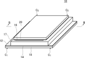
- FIG. 1A is a schematic perspective view showing an example of an electroacoustic conversion film original fabric according to the first embodiment of the present invention
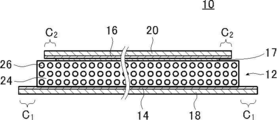
- FIG. 1B is a cross-sectional view taken along the line BB of FIG. 1A.
- An electroacoustic conversion film original fabric (hereinafter also referred to as “conversion film original fabric”) 10 shown in FIGS. 1A and 1B basically includes a piezoelectric layer 12 that expands and contracts in accordance with the state of an electric field, and a piezoelectric layer 12.
- the conversion film original fabric 10 has an area of the lower thin film electrode 14 when viewed from a direction perpendicular to the main surface of the piezoelectric layer 12.
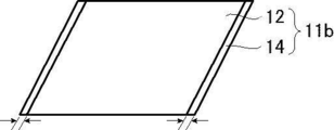
- the unbonded portion C 1 where the piezoelectric layer 12 is not laminated is provided on each side of the two opposing edges of the lower thin film electrode 14 that is larger than the area. That is, the width of the lower thin film electrode 14 in the left-right direction in FIG. 1B is larger than the width of the piezoelectric layer 12.
- the area of the upper thin film electrode 16 when viewed from the direction perpendicular to the main surface of the piezoelectric layer 12 is slightly smaller than the area of the piezoelectric layer 12, and the piezoelectric layer 12 and the upper thin film electrode 16.
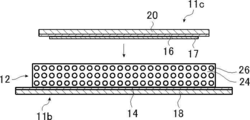
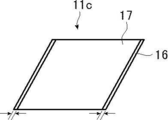
- the area of the upper thin film electrode 16 is larger than the area of the adhesive layer 17, and the width of the upper thin film electrode 16 in the left-right direction in FIG. It is larger than 17 width. Therefore, the upper thin film electrode 16 has a region where the adhesive layer 17 is not formed on each of the two opposing edges, that is, an unbonded portion C 2 that is not bonded to the piezoelectric layer 12.
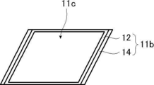
- the unbonded portion C 1 of the lower thin-film electrode 14 and the unbonded portion C 2 of the upper thin-film electrode 16 each extend in a direction parallel to the end side on the side to be formed, and one of the adjacent ones adjacent to this end side It is formed in the region from the end side to the other end side, that is, the entire region in the longitudinal direction on the end side. Further, the two unbonded portions C 1 and the two unbonded portions C 2 are both formed on the two opposing side edges of the piezoelectric layer 12.
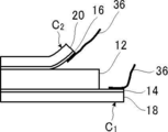
- the unbonded portion C 1 of the lower thin film electrode 14 and the unbonded portion C 2 of the upper thin film electrode 16 are portions to which the wirings 36 are connected, that is, electrode lead portions. By connecting the wiring 36 to the electrode lead portion, the thin film electrode and an external device can be electrically connected.
- the unadhered portion C 1 and the unadhered portion C 2 serving as the electrode lead-out portions are prevented from damaging the thin film electrode, and the number of work steps is reduced. Cost can be reduced and formed. This will be described in detail later.
- the unbonded portions C 1 and unbonded portion C 2 so provided in the entire region of at least one end of the thin film electrode, in making the conversion film of the wide variety of shapes, cut to convert raw film material produced
- the position of the electrode lead-out portion can be freely determined, and the degree of freedom in design is high, so that productivity can be increased.
- the width in the direction perpendicular to the corresponding edge of each of the non-bonded portion C 1 and the non-bonded portion C 2 is not particularly limited, but a substantial drive surface that facilitates connection to the wiring is provided. From the viewpoint of securing the size, 5 to 20 mm is preferable, and 8 to 15 mm is more preferable.
- the lower thin film electrode 14 has two unbonded portions C 1.
- the present invention is not limited to this, and it is only necessary to have at least one unbonded portion C 1 .
- An unbonded portion C 1 may be provided on each of the four end sides of the lower thin film electrode 14 to have four unbonded portions C 1 .
- the upper thin film electrode 16 has two unbonded portions C 2.
- the unbonded portion C 2 may be provided on each of the four end sides of the upper thin film electrode 16 to have four unbonded portions C 2 .
- the two unbonded portions C 1 are provided on the two opposing edge sides.
- the present invention is not limited to this, and the two unbonded portions C 1 It is good also as a structure provided in an edge side.
- two unbonded portions C 2 may also be provided in two adjacent end sides.
- the greater the number of unbonded portions the higher the degree of freedom in design when producing the electroacoustic conversion film having a desired shape by cutting the produced electroacoustic conversion film original.
- the unbonded portion is provided on three or more sides, or when two unbonded portions are provided on the two adjacent sides, it is difficult to apply a so-called roll-to-roll manufacturing process. May become complicated. Therefore, it is preferable that the two unbonded portions are provided on the two opposite sides.
- the unbonded portion C 1 of the lower thin film electrodes 14, and the unbonded portion C 2 of the upper thin film electrode 16, a configuration which is formed at the same end side of the piezoelectric layer 12,
- the present invention is not limited to this, and the unbonded portion C 1 and the unbonded portion C 2 may be formed on different end sides of the piezoelectric layer 12.
- the upper thin film electrode 16 is bonded to the piezoelectric layer 12 via the adhesive layer 17, but the present invention is not limited to this, and the upper thin film electrode 16 does not have the adhesive layer 17. 16 and the piezoelectric layer 12 may be directly bonded by pressure bonding or the like.
- the 2nd aspect of the electroacoustic conversion film original fabric of this invention is demonstrated.
- the second aspect of the original electroacoustic conversion film according to the present invention is formed on each of the dielectric layers, the two thin film electrodes formed on both surfaces of the piezoelectric layer, and the two thin film electrodes, respectively.
- An electroacoustic conversion film original having two protective layers, each of which has an area smaller than the area of the piezoelectric layer when viewed from a direction perpendicular to the main surface of the piezoelectric layer.
- the electroacoustic conversion film original fabric which has the non-bonding part which is not adhere
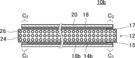
- FIG. 3 is a schematic cross-sectional view showing an example of the electroacoustic conversion film original fabric according to the second aspect of the present invention.
- 3 includes a piezoelectric layer 12, a lower thin film electrode 14b provided on one surface of the piezoelectric layer 12, a lower protective layer 18b provided on the surface of the lower thin film electrode 14b, and a piezoelectric layer.
- the upper thin film electrode 16 is provided on the other surface of the upper thin film electrode 12, and the upper protective layer 20 is provided on the surface of the upper thin film electrode 16.
- the conversion film original fabric 10b shown in FIG. 3 has the conversion shown in FIG.
- the area of the lower thin film electrode 14b when viewed from the direction perpendicular to the main surface of the piezoelectric layer 12 is smaller than the area of the piezoelectric layer 12,
- the piezoelectric layer 12 and the lower thin film electrode 14b are bonded via an adhesive layer 15, and the area of the lower thin film electrode 14b is larger than the area of the adhesive layer 15 and the lower thin film electrode 14b is opposed to the two.
- An unbonded portion C 1 which is a region where the adhesive layer 15 is not formed, is provided on each end side. That is, the lower thin film electrode 14 b and the lower protective layer 18 b have the same configuration as the upper thin film electrode 16 and the upper protective layer 20 except that they are stacked on the opposite surface of the piezoelectric layer 12.
- the unadhered portion C 1 and the unadhered portion C 2 are prevented from being damaged by the thin film electrode. Moreover, it can be formed by reducing the number of work steps and cost.
- the conversion original film of the second aspect also, the unbonded portion C 1 and unbonded portion C 2, so provided in the entire region of at least one end of the thin-film electrode, making the conversion film of the wide variety of shapes.
- the position of the electrode lead-out portion can be freely determined, and the degree of freedom in design is high, so that the productivity can be increased. .
- the electroacoustic conversion film of the present invention (hereinafter also referred to as “conversion film”) is a conversion film obtained by cutting (cutting) the above-mentioned conversion film original fabric into a desired shape, and is an unadhered portion of the thin film electrode. It has a shape that leaves at least a portion (see FIG. 8). Therefore, the conversion film of the present invention comprises a dielectric piezoelectric layer, two thin film electrodes formed on both sides of the piezoelectric layer, and two protective layers formed on the two thin film electrodes, respectively.
- the conversion film original fabric of the present invention can be used as a conversion film as it is without being cut.
- the piezoelectric layer 12 is a layer that has piezoelectricity and expands and contracts in the in-plane direction according to the state of the electric field.
- 1B and FIG. 3 is a polymer composite piezoelectric material in which piezoelectric particles 26 are dispersed in a matrix 24 made of a polymer material.
- the piezoelectric layer 12 is polarized.
- the piezoelectric particles 26 in the piezoelectric layer 12 may be dispersed in the viscoelastic matrix 24 with regularity or irregularly.
- a polymer material having viscoelasticity at room temperature is preferably used as a material of the matrix 24 (matrix and binder) of the polymer composite piezoelectric body constituting the piezoelectric layer 12.
- the polymer composite piezoelectric body (piezoelectric layer 12) used for the conversion film raw material of the present invention preferably has the following requirements. Therefore, it is preferable to use a polymer material having viscoelasticity at room temperature as a material having the following requirements.
- “normal temperature” refers to a temperature range of about 0 to 50 ° C.
- the speaker vibrates the piezoelectric particles at an audio band frequency of 20 Hz to 20 kHz, and the vibration plate (polymer composite piezoelectric material) vibrates as a whole by the vibration energy, so that sound is reproduced.
- the polymer composite piezoelectric body is required to have an appropriate hardness.
- the frequency characteristic of the speaker is smooth, the amount of change in the sound quality when the lowest resonance frequency f 0 with the change in the curvature is changed becomes small. Therefore, the loss tangent of the polymer composite piezoelectric material is required to be moderately large.
- the polymer composite piezoelectric material used in the original film of the conversion film of the present invention is required to behave hard to vibrations of 20 Hz to 20 kHz and soft to vibrations of several Hz or less.
- the loss tangent of the polymer composite piezoelectric body is required to be reasonably large with respect to vibrations of all frequencies of 20 kHz or less.
- polymer solids have a viscoelastic relaxation mechanism, and as the temperature increases or the frequency decreases, large-scale molecular motion decreases (relaxes) the storage elastic modulus (Young's modulus) or maximizes the loss elastic modulus (absorption). As observed. Among them, the relaxation caused by the micro Brownian motion of the molecular chain in the amorphous region is called main dispersion, and a very large relaxation phenomenon is observed. The temperature at which this main dispersion occurs is the glass transition point (Tg), and the viscoelastic relaxation mechanism appears most remarkably.
- Tg glass transition point
- a polymer material having a glass transition point at room temperature in other words, a polymer material having viscoelasticity at room temperature is used as a matrix, so that vibrations of 20 Hz to 20 kHz can be prevented.
- a polymer composite piezoelectric material that is hard and softly behaves with respect to slow vibrations of several Hz or less is realized.
- a polymer material having a glass transition temperature at a frequency of 1 Hz at room temperature that is, 0 to 50 ° C., is preferably used for the matrix of the polymer composite piezoelectric material in terms of suitably exhibiting this behavior.
- a polymer material having viscoelasticity at room temperature Preferably, a polymer material having a maximum value of loss tangent Tan ⁇ at a frequency of 1 Hz in a dynamic viscoelasticity test at room temperature, that is, 0 to 50 ° C., is 0.5 or more.
- a polymer material having a maximum value of loss tangent Tan ⁇ at a frequency of 1 Hz in a dynamic viscoelasticity test at room temperature that is, 0 to 50 ° C.
- the polymer material preferably has a storage elastic modulus (E ′) at a frequency of 1 Hz as measured by dynamic viscoelasticity of 100 MPa or more at 0 ° C. and 10 MPa or less at 50 ° C.
- E ′ storage elastic modulus
- the polymer material has a relative dielectric constant of 10 or more at 25 ° C.
- the polymer material preferably has a relative dielectric constant of 10 or less at 25 ° C.
- Polymer materials satisfying such conditions include cyanoethylated polyvinyl alcohol (cyanoethylated PVA), polyvinyl acetate, polyvinylidene chloride core acrylonitrile, polystyrene-vinyl polyisoprene block copolymer, polyvinyl methyl ketone, and polybutyl. Examples include methacrylate.
- cyanoethylated polyvinyl alcohol cyanoethylated PVA
- polyvinyl acetate polyvinylidene chloride core acrylonitrile
- polystyrene-vinyl polyisoprene block copolymer polyvinyl methyl ketone
- polybutyl examples include methacrylate.
- these polymer materials commercially available products such as Hibler 5127 (manufactured by Kuraray Co., Ltd.) can also be suitably used.
- Hibler 5127 manufactured by Kuraray Co., Ltd.
- the matrix 24 using the polymer material having viscoelasticity at room temperature may use a plurality of polymer materials in combination as necessary. That is, other dielectric polymer materials may be added to the matrix 24 as needed in addition to viscoelastic materials such as cyanoethylated PVA for the purpose of adjusting dielectric properties and mechanical properties.
- dielectric polymer materials examples include polyvinylidene fluoride, vinylidene fluoride-tetrafluoroethylene copolymer, vinylidene fluoride-trifluoroethylene copolymer, and polyvinylidene fluoride-trifluoroethylene copolymer.
- Fluorine polymers such as polyvinylidene fluoride-tetrafluoroethylene copolymer, vinylidene cyanide-vinyl acetate copolymer, cyanoethyl cellulose, cyanoethyl hydroxy saccharose, cyanoethyl hydroxy cellulose, cyanoethyl hydroxy pullulan, cyanoethyl methacrylate, cyanoethyl acrylate, cyanoethyl Hydroxyethyl cellulose, cyanoethyl amylose, cyanoethyl hydroxypropyl cellulose, cyanoethyl dihydroxypropyl cellulose, Synthesis of polymers having cyano groups or cyanoethyl groups, such as noethyl hydroxypropyl amylose, cyanoethyl polyacrylamide, cyanoethyl polyacrylate, cyanoethyl pullulan, cyanoethyl polyhydroxy
- Examples thereof include rubber.
- a polymer material having a cyanoethyl group is preferably used.
- the dielectric polymer added to the matrix 24 of the piezoelectric layer 12 in addition to the material having viscoelasticity at room temperature such as cyanoethylated PVA is not limited to one type, and a plurality of types may be added. .
- thermoplastic resins such as vinyl chloride resin, polyethylene, polystyrene, methacrylic resin, polybutene, isobutylene, phenol resin, urea resin, melamine resin, Thermosetting resins such as alkyd resins and mica may be added.
- a tackifier such as rosin ester, rosin, terpene, terpene phenol, petroleum resin, etc. may be added.
- the addition amount when a polymer other than a viscoelastic material such as cyanoethylated PVA is added but it is 30% by weight or less in the ratio of the matrix 24. preferable.
- the characteristics of the polymer material to be added can be expressed without impairing the viscoelastic relaxation mechanism in the matrix 24, so that the dielectric constant is increased, the heat resistance is improved, the adhesion with the piezoelectric particles 26 and the electrode layer is improved, and the like. In this respect, preferable results can be obtained.
- the material of the matrix 24 is not limited to a polymer material having viscoelasticity at room temperature, and the above-described dielectric polymer can also be used.
- the piezoelectric particles 26 are made of ceramic particles having a perovskite type or wurtzite type crystal structure.
- the ceramic particles constituting the piezoelectric particles 26 include lead zirconate titanate (PZT), lead lanthanum zirconate titanate (PLZT), barium titanate (BaTiO3), zinc oxide (ZnO), and titanium.
- PZT lead zirconate titanate
- PLATiO3 barium titanate
- ZnO zinc oxide
- titanium titanium.
- Examples thereof include a solid solution (BFBT) of barium acid and bismuth ferrite (BiFe3).
- the particle diameter of the piezoelectric particles 26 may be appropriately selected according to the size of the conversion film original fabric and the application, but is preferably 1 to 10 ⁇ m according to the study of the present inventors. By setting the particle size of the piezoelectric particles 26 within the above range, a favorable result can be obtained in terms of achieving both high piezoelectric characteristics and flexibility.
- the piezoelectric particles 26 in the piezoelectric layer 12 are uniformly dispersed in the matrix 24 with regularity, but may be irregularly dispersed.
- the amount ratio between the matrix 24 and the piezoelectric particles 26 in the piezoelectric layer 12 is the size and thickness of the conversion film original fabric in the surface direction, the use of the conversion film original fabric, What is necessary is just to set suitably according to the characteristic etc. which are requested
- the volume fraction of the piezoelectric particles 26 in the piezoelectric layer 12 is preferably 30 to 70%, particularly preferably 50% or more. 70% is more preferable.
- the thickness of the piezoelectric material layer 12 is preferably 5 to 100 ⁇ m, more preferably 5 to 50 ⁇ m, and particularly preferably 5 to 30 ⁇ m.
- the piezoelectric layer 12 is preferably polarized (polled) as described above. The polarization process will be described in detail later.
- a polymer composite piezoelectric body is used as the piezoelectric layer 12, but the present invention is not limited to this, and a piezoelectric polymer piezoelectric having a piezoelectric property such as PVDF (polyvinylidene fluoride). Materials may be used. Note that uniaxially stretched PVDF has in-plane anisotropy in its piezoelectric properties, whereas polymer composite piezoelectric bodies do not have in-plane anisotropy. It is preferable in that it can be converted into a back-and-forth motion and a sufficient volume and sound quality can be obtained.
- PVDF polyvinylidene fluoride
- the conversion film original fabric of the present invention has a piezoelectric layer 12 sandwiched between a lower thin film electrode 14 and an upper thin film electrode 16, and this laminate is covered with a lower protective layer 18 and an upper protective layer 20. It has the structure formed by pinching.
- the lower protective layer 18 and the upper protective layer 20 have a role of imparting appropriate rigidity and mechanical strength to the polymer composite piezoelectric body. That is, in the original film of the conversion film of the present invention, the polymer composite piezoelectric body (piezoelectric layer 12) composed of the matrix 24 and the piezoelectric particles 26 has a very excellent flexibility against a slow bending deformation.
- a lower protective layer 18 and an upper protective layer 20 are provided. Note that the lower protective layer 18 and the upper protective layer 20 have the same configuration except for the arrangement position and size, and therefore it is necessary to distinguish the lower protective layer 18 and the upper protective layer 20 in the following description. If not, both members are collectively referred to as a protective layer.
- the protective layer is not particularly limited, and various sheet materials can be used, and various resin films (plastic films) are preferably exemplified as an example.
- various resin films plastic films
- PET polyethylene terephthalate
- PP polypropylene
- PS polystyrene
- PC polycarbonate
- PPS polyphenylene sulfite
- PMMA polymethyl methacrylate
- PEI Polyetherimide
- PEI polyimide
- PI polyimide
- PEN polyethylene naphthalate
- TAC triacetyl cellulose
- cyclic olefin-based resin are preferably used.
- the thickness of the protective layer is basically the same, but may be different.
- the rigidity of the protective layer is too high, not only the expansion and contraction of the piezoelectric layer 12 is restricted, but also the flexibility is impaired, so that mechanical strength and good handling properties as a sheet-like material are required.
- the thinner the protective layer the more advantageous.
- the thickness of the protective layer is not more than twice the thickness of the piezoelectric layer 12, it is possible to ensure both rigidity and appropriate flexibility.
- the thickness of the lower protective layer 18 and the upper protective layer 20 is preferably 100 ⁇ m or less, and preferably 50 ⁇ m or less. More preferably, it is preferably 25 ⁇ m or less.
- the lower thin film electrode 14 is provided between the piezoelectric layer 12 and the lower protective layer 18, and the upper thin film electrode 16 is provided between the piezoelectric layer 12 and the upper protective layer 20, respectively. It is formed.
- the lower thin film electrode 14 and the upper thin film electrode 16 are provided for applying a voltage to the piezoelectric layer 12.
- the lower thin film electrode 14 and the upper thin film electrode 16 are the same except for the size and the arrangement position. Therefore, it is necessary to distinguish the lower thin film electrode 14 and the upper thin film electrode 16 in the following description. If not, both members are collectively referred to as a thin film electrode.
- the material for forming the thin film electrode is not particularly limited, and various conductors can be used. Specific examples include carbon, palladium, iron, tin, aluminum, nickel, platinum, gold, silver, copper, chromium and molybdenum, alloys thereof, indium tin oxide, and the like. Among them, any of copper, aluminum, gold, silver, platinum, and indium tin oxide is preferably exemplified.
- the method for forming the thin film electrode is not particularly limited, and vapor deposition methods (vacuum film forming methods) such as vacuum vapor deposition and sputtering, film formation by plating, and a method of attaching a foil formed of the above materials Various known methods can be used.
- a thin film of copper or aluminum formed by vacuum vapor deposition is preferably used as a thin film electrode because the flexibility of the original film of the conversion film can be ensured.
- a copper thin film formed by vacuum deposition is particularly preferably used.
- the thickness of the thin film electrode is basically the same, but may be different.
- the thin film electrode has an excessively high electrical resistance. If it is not in the range, the thinner the film, the more advantageous.
- the thickness of the thin film electrode and the Young's modulus is less than the product of the thickness of the protective layer and the Young's modulus, the flexibility is not greatly impaired. It is.
- the protective layer is a combination of PET (Young's modulus: about 6.2 GPa) and the thin film electrode is made of copper (Young's modulus: about 130 GPa)
- the thickness of the protective layer is 25 ⁇ m
- the thickness of the thin film electrode is It is preferably 1.2 ⁇ m or less, more preferably 0.3 ⁇ m or less, and particularly preferably 0.1 ⁇ m or less.
- the piezoelectric layer 12 (polymer composite piezoelectric body) in which the piezoelectric particles 26 are dispersed in the matrix 24 is sandwiched between the lower thin film electrode 14 and the upper thin film electrode 16.
- the laminate is configured to be sandwiched between the lower protective layer 18 and the upper protective layer 20.
- Such a conversion film original fabric of the present invention preferably has a maximum value at room temperature at which the loss tangent (Tan ⁇ ) at a frequency of 1 Hz by dynamic viscoelasticity measurement is 0.5 or more.
- the conversion film raw material of the present invention preferably has a storage elastic modulus (E ′) at a frequency of 1 Hz as measured by dynamic viscoelasticity of 10 to 30 GPa at 0 ° C. and 1 to 10 GPa at 50 ° C.
- the conversion film original fabric can have a large frequency dispersion in the storage elastic modulus (E ′) at room temperature. That is, it can behave hard for vibrations of 20 Hz to 20 kHz and soft for vibrations of several Hz or less.
- the original film of the conversion film according to the present invention has a product of thickness and storage elastic modulus (E ′) at a frequency of 1 Hz as measured by dynamic viscoelasticity at 1.0 ° C. to 2.0 ⁇ 10 6 at 0 ° C. 6 (1.0E + 06 to 2.0E + 06) N / m, preferably 1.0 ⁇ 10 5 to 1.0 ⁇ 10 6 (1.0E + 05 to 1.0E + 06) N / m at 50 ° C.
- E ′ thickness and storage elastic modulus
- the conversion film original fabric of the present invention preferably has a loss tangent (Tan ⁇ ) at 25 ° C. and a frequency of 1 kHz of 0.05 or more in a master curve obtained from dynamic viscoelasticity measurement.
- Tan ⁇ loss tangent
- conversion film original frequency characteristic of the loudspeaker using the conversion film cut out from the anti becomes smooth, it can vary the amount of sound is also small when the lowest resonance frequency f 0 with the change in the curvature of the speaker has changed.
- the method for producing an electroacoustic conversion film raw material of the present invention includes a piezoelectric layer having dielectric properties, two thin film electrodes formed on both surfaces of the piezoelectric layer, and two formed on each of the two thin film electrodes.
- a method for producing an electroacoustic conversion film original having a protective layer A preparation step of preparing an electrode laminate in which one thin film electrode and one protective layer are laminated; and Having a lamination process of laminating an electrode laminate and a piezoelectric layer; In the laminating step, when the electrode laminate and the piezoelectric layer are laminated, at least one end of the thin film electrode is provided with an unadhered portion that is not bonded to the piezoelectric layer.
- a coating composition to be a piezoelectric layer is applied on the thin film electrode of the electrode laminate, and then cured to form a piezoelectric layer, and the electrode laminate and the piezoelectric layer are laminated.
- a first lamination that forms an unadhered portion by applying at least one end of the thin-film electrode as a coating-unapplied portion where the coating composition is not applied when applying the coating composition.
- the electrode laminate is laminated on both surfaces of the piezoelectric layer. Therefore, as the lamination process, the first lamination process is performed when the electrode laminate is laminated on one surface of the piezoelectric layer, and the second lamination process is performed when the electrode laminate is laminated on the other surface. Alternatively, both surfaces may be laminated in the second lamination step.
- FIGS. 4A to 4E are conceptual diagrams for explaining an example of the manufacturing method of the present invention
- FIGS. 5A to 5C are schematic perspective views for explaining the second stacking step.
- the manufacturing method of the present invention will be described by explaining a manufacturing method for producing the electroacoustic conversion film original fabric 10 shown in FIGS. 1A and 1B.
- the preparation step is a step of preparing an electrode laminate in which one thin film electrode and one protective layer are laminated.
- a lower electrode laminated body 11a that is a sheet-like material in which a lower thin film electrode 14 and a lower protective layer 18 are laminated is prepared.
- the upper electrode laminated body 11c which is a sheet-like object formed by laminating the upper thin film electrode 16 and the upper protective layer 20 shown in FIG. 4E is prepared.
- the lower electrode laminated body 11a may be produced by forming a copper thin film or the like as the lower thin film electrode 14 on the surface of the lower protective layer 18 by vacuum deposition, sputtering, plating, or the like.
- the upper electrode laminated body 11c may be manufactured by forming a copper thin film or the like as the upper thin film electrode 16 on the surface of the upper protective layer 20 by vacuum deposition, sputtering, plating, or the like.
- the main surface of the upper electrode stack 11c is smaller than the main surface of the lower electrode stack 11a.
- the length of one of the main surface of the upper electrode stack 11c and the main surface of the lower electrode stack 11a is the same, and the other is different.
- a protective layer with a separator temporary support
- PET or the like having a thickness of 25 to 100 ⁇ m can be used.
- separator PET or the like having a thickness of 25 to 100 ⁇ m can be used.
- what is necessary is just to remove a separator after lamination
- a coating composition to be a piezoelectric layer is applied onto the thin film electrode of the electrode stack, and then cured to form a piezoelectric layer, and the electrode stack and the piezoelectric layer are stacked. It is a process.
- at the time of applying the coating composition in the first laminating step at least one end of the thin film electrode is set as a non-coating portion where the coating composition is not applied, so that the coating composition is not adhered. Forming part.
- a coating composition obtained by dissolving a polymer material as a matrix material such as cyanoethylated PVA in an organic solvent, further adding piezoelectric particles 26 such as PZT particles, and stirring and dispersing.
- the organic solvent is not particularly limited, and various organic solvents can be used.
- this paint is cast (applied) on the lower thin film electrode 14 side of the lower electrode laminate 11a, and the organic solvent is evaporated and dried. To do.
- a laminated body 11b having the lower thin film electrode 14 on the lower protective layer 18 and the piezoelectric layer 12 formed on the lower thin film electrode 14 is produced.
- the coating composition when the coating composition is applied, it is not applied to the entire surface of the electrode laminate on the side of the lower thin film electrode, but applied only to a part of the thin film. At least one end portion of the electrode (electrode laminate) is a coating-uncoated portion where the coating composition is not applied.
- the coating composition is not applied to the two opposing side edges of the lower electrode laminate 11a without applying the coating composition. Forming.
- This paint non-application part becomes the non-adhered part C 1 of the conversion film original fabric 10 shown in FIG. 1B.
- the paint casting method is not particularly limited, and any known method (coating apparatus) such as a slide coater or a doctor knife can be used.
- the method of applying the coating composition only to a partial region on the lower thin film electrode 14 side of the lower electrode laminate 11a there is no particular limitation on the method of applying the coating composition only to a partial region on the lower thin film electrode 14 side of the lower electrode laminate 11a.
- the width of the slit opening to be discharged may be adjusted to be smaller than the width of the lower thin film electrode 14. Or you may mask and apply
- the matrix 24 may be added with a polymer piezoelectric material such as PVDF in addition to a viscoelastic material such as cyanoethylated PVA.
- a polymer piezoelectric material such as PVDF
- a viscoelastic material such as cyanoethylated PVA.
- the polymer piezoelectric material to be added to the paint may be dissolved.
- the laminated body 11b which has the lower thin film electrode 14 on the lower protective layer 18, and forms the piezoelectric material layer 12 on the lower thin film electrode 14 is produced, Preferably, the polarization process (polling) of the piezoelectric material layer 12 is carried out. )I do.
- the method for polarization treatment of the piezoelectric layer 12 is not particularly limited, and a known method can be used. As a preferable method of polarization treatment, the method shown in FIGS. 4C and 4D is exemplified.
- a bar or wire shape that is movable along the upper surface 12a with a gap g of, for example, 1 mm on the upper surface 12a of the piezoelectric layer 12 of the multilayer body 11b.
- Corona electrode 30 is provided. Then, the corona electrode 30 and the lower thin film electrode 14 are connected to a DC power source 32. Further, a heating means for heating and holding the stacked body 11b, for example, a hot plate is prepared.
- the piezoelectric layer 12 is heated and held at, for example, a temperature of 100 ° C., and is several kV, for example, 6 kV, between the DC power source 32 and the lower thin film electrode 14 and the corona electrode 30.
- a DC voltage is applied to cause corona discharge.
- the corona electrode 30 is moved (scanned) along the upper surface 12a of the piezoelectric layer 12 while maintaining the gap g, and the piezoelectric layer 12 is polarized.
- the corona electrode 30 may be moved by using a known rod-like moving means.
- the method for moving the corona electrode 30 is not limited. That is, the corona electrode 30 may be fixed and a moving mechanism for moving the stacked body 11b may be provided, and the stacked body 11b may be moved to perform the polarization treatment.
- the laminate 11b may be moved by using a known sheet moving means.
- the number of corona electrodes 30 is not limited to one, and a plurality of corona electrodes 30 may be used to perform corona poling treatment.
- the polarization process is not limited to the corona polling process, and normal electric field poling in which a direct current electric field is directly applied to a target to be polarized can also be used.
- normal electric field poling it is necessary to form the upper thin film electrode 16 before the polarization treatment.
- the second lamination step is a step of laminating the electrode laminate and the piezoelectric layer by bonding the piezoelectric layer and the thin film electrode side of the electrode laminate.
- stacking process it is a process of forming an unbonded part by making at least 1 edge part of a thin film electrode into the unbonded part which does not bond with a piezoelectric material layer.
- the second lamination step includes an adhesive application step of applying an adhesive to the thin film electrode side of the electrode laminate, and a bonding in which the piezoelectric layer and the electrode laminate are bonded via the adhesive. In the adhesive application step, at least one end portion of the thin film electrode is used as an adhesive non-applied portion where no adhesive is applied, thereby forming an unadhered portion.
- the adhesive application process While performing the polarization treatment of the piezoelectric layer 12 of the multilayer body 11b, it is bonded to the upper electrode multilayer body 11c, which is a sheet-like material in which the upper thin film electrode 16 is formed on the upper protective layer 20 prepared in the preparation process.
- the adhesive layer 17 is formed by applying the agent.
- the adhesive application step when applying the adhesive, the adhesive is not applied to the entire main surface of the upper thin film electrode 16, but applied only to a part of the region, and at least one of the upper thin film electrodes 16 is applied. One end is defined as an adhesive-unapplied portion where no adhesive is applied.
- two adhesive non-applied portions are formed on the two opposing side edges of the upper electrode laminate 11c without applying the adhesive. Uncoated portions this adhesive, the unbonded portion C 2 of the converted raw film material 10 shown in FIG. 1B.
- the material of the adhesive is not particularly limited, and a known adhesive used for bonding the piezoelectric layer and the thin film electrode in the conversion film can be appropriately used.
- a polymer composite piezoelectric material in which piezoelectric particles are dispersed in a matrix made of a polymer material is used as the piezoelectric layer, the same polymer material as the matrix material may be used as an adhesive.
- the bonding step the upper thin film electrode 16 side on which the adhesive layer 17 is formed faces the piezoelectric layer 12, and the upper electrode laminate 11 c is moved to the piezoelectric layer 12.
- the conversion film original fabric 10 is produced by laminating the laminated body 11b that has been subjected to the polarization treatment.
- the adhesive-unapplied portion where the adhesive layer 17 is not formed in the upper electrode laminate 11 c is not bonded to the piezoelectric layer 12, and thus becomes the unbonded portion C 2 of the conversion film original fabric 10.
- a piezoelectric film used as a thin speaker needs to be thinned not only from the viewpoint of thinning the speaker, but also from the viewpoint of responsiveness and widening of a reproducible band.
- a thin electrode layer such as a vapor deposition film
- wiring to the thin film electrode needs to be performed while ensuring insulation between the thin film electrodes on both sides of the piezoelectric layer, but it is not easy because the thickness of the piezoelectric layer is as thin as about several tens of ⁇ m.
- the electrode laminate has a structure in which the electrode lead-out part protrudes in a convex shape outside the surface of the piezoelectric layer, so that the electrode can be drawn out from the thin-film electrode and wiring can be easily connected by soldering. Furthermore, this electrode can be pulled out while ensuring insulation between the thin film electrodes on both sides.
- the piezoelectric layer is rubbed with a cotton swab or the like soaked in a solvent to dissolve and remove part of the piezoelectric layer, thereby protruding the electrode
- the thin film electrode may be damaged, for example, the thin film electrode may be melted.
- the electrode lead-out portion is formed in a shape protruding in a convex shape, it is necessary to determine the position of the electrode lead-out portion in advance when producing the electroacoustic conversion film. The position of the part cannot be changed.
- the manufacturing method of the present invention provides an unbonded portion that is not bonded to the piezoelectric layer at least one end of the thin film electrode when the electrode stack and the piezoelectric layer are stacked in the stacking step. It has a configuration. Specifically, when applying a coating composition to be a piezoelectric layer on a thin film electrode, at least one end of the thin film electrode is a coating-uncoated portion where the coating composition is not applied. The unbonded part is formed. Or when laminating
- the thin film electrode forms an unbonded portion that is not bonded to the piezoelectric layer, so there is no need to dissolve and remove the piezoelectric layer. Therefore, the thin film electrode is not damaged.
- the unbonded portion is formed at the same time in the step of laminating the piezoelectric layer and the thin film electrode, it is possible to suppress an increase in work man-hours and suppress an increase in equipment investment and cost.
- the method for laminating the piezoelectric layer and the electrode laminate in the second laminating step is not limited to a method using an adhesive.
- the original film of the conversion film may be produced by thermocompression bonding the piezoelectric layer and the electrode laminate with a heating press device, a heating roller pair, or the like.
- an unbonded portion is formed by forming at least one end of the electrode stack (thin film electrode) as a non-crimped portion that is not pressure-bonded to the piezoelectric layer. That's fine.
- mask members 80 are disposed at both ends of the upper electrode laminate 11c, and the piezoelectric layer 12 and the upper electrode laminate 11c are pressure-bonded and masked by the mask member 80.
- the piezoelectric layer 12 and the upper electrode laminate 11c in a region other than the region may be bonded to form an unbonded portion in the masked region of the upper electrode laminate 11c.
- 7A shows an example in which the unbonded portion of the upper electrode stack 11c (upper thin film electrode 16) and the unbonded portion of the lower thin film electrode 14 are formed on the same edge side of the piezoelectric layer 12.
- FIG. 7B shows an example in which the unbonded portion of the upper thin film electrode 16 and the unbonded portion of the lower thin film electrode 14 are formed on different end sides of the piezoelectric layer 12. is there.
- the width of the unbonded portion formed in the first stacking step and the width of the unbonded portion formed in the second stacking step are preferably 5 to 20 mm, and more preferably 8 to 15 mm. .
- two unbonded portions are formed on the two facing edge sides, but the present invention is not limited thereto, and at least one edge side is formed.
- An unbonded portion may be formed on the side, or an unbonded portion may be formed on each of the four end sides.
- the manufacturing method of the present invention can easily form an unbonded portion serving as an electrode lead-out portion without damaging the thin film electrode even when the electrode laminate is thin. From this point, the manufacturing method of the present invention can be more suitably applied when the thickness of the electrode laminate is 4 to 20 ⁇ m.
- the manufacturing method of the present invention is not limited to this, and both sides are electrodes by the second laminating step.
- the conversion film original fabric 10b as shown in FIG. 3 may be produced by laminating the laminate.
- the method for producing an electroacoustic conversion film of the present invention is a production method having a cutting step of cutting the conversion film original fabric produced by the above-described method for producing an electroacoustic conversion film into a predetermined shape.
- the thin film electrode is cut into a shape that leaves at least part of the unbonded portion.
- the cutting step is a step of cutting the conversion film original fabric 10 in which the electrode laminate is laminated on both surfaces of the piezoelectric layer in the lamination step into a predetermined shape.
- the conversion film original fabric 10 is cut into a shape that leaves at least a part of the unbonded portion C 1 of the lower thin film electrode 14 and the unbonded portion C 2 of the upper thin film electrode 16.
- the example shown in FIG. 8 shows the example which cut
- the conversion film original fabric is cut into a conversion film so as to include the unbonded portions C 1 and C 2 of the portion indicated by a in the drawing.
- the conversion film thus produced has a piezoelectric layer, two thin film electrodes, and a region where the two protective layers have the same shape and are bonded to each other, and the piezoelectric layer, the two thin film electrodes, In addition, the two protective layers overlap each other in the stacking direction, and the piezoelectric layer and the two thin film electrodes have a region that is not bonded to each other. A region where the piezoelectric layer and the two thin film electrodes are not bonded to each other can be used as an electrode lead-out portion.
- the predetermined shape is a desired shape according to the shape of the thin speaker to be used. Moreover, there is no limitation in particular in the shape (predetermined shape) of the conversion film cut
- the conversion film original fabric produced by the production method of the present invention has an unadhered portion in the entire region of at least one end of the thin film electrode, when producing the conversion film, the unadhered portion of the conversion film original fabric
- the position of the electrode lead-out part can be freely determined, it can be formed in the desired shape, and the degree of freedom in design is high, so it is diverse
- a conversion film having a simple shape can be easily produced, and productivity can be increased.
- FIG. 9A is a schematic cross-sectional view showing an example of an electroacoustic transducer using the conversion film of the present invention
- FIG. 9B is a top view of FIG. 9A. That is, FIG. 9A is a cross-sectional view taken along line aa of FIG. 9B.
- the electroacoustic transducer 40 shown in FIGS. 9A and 9B is a flat plate type piezoelectric speaker using the above-described conversion film 44 of the present invention as a speaker diaphragm for converting an electric signal into vibration energy.
- the piezoelectric speaker 40 can also be used as a microphone, a musical instrument sensor, or the like.
- the illustrated piezoelectric speaker 40 basically includes a conversion film 44 (piezoelectric film), a case 42, a viscoelastic support 46, and a frame 48.
- the conversion film 44 is a conversion film formed by cutting out a substantially rectangular shape from the conversion film original fabric of the present invention.
- the case 42 is a thin square tube-shaped housing that is made of plastic or the like and that is open on one side.
- the case 42 (that is, the piezoelectric speaker) is not limited to a square tube shape, and various cases such as a cylindrical shape or a rectangular tube shape having a rectangular bottom surface. Is available.
- the frame body 48 is a plate material having an opening at the center and having the same shape as the upper end surface (open surface side) of the case 42.
- the viscoelastic support 46 has an appropriate viscosity and elasticity, supports the conversion film 44, and gives a constant mechanical bias everywhere on the conversion film, so that the expansion and contraction movement of the conversion film is not wasted. This is to convert the movement back and forth (movement in a direction perpendicular to the film surface).
- nonwoven fabrics such as wool felt, wool felt including rayon and PET, foamed materials (foamed plastics) such as glass wool or polyurethane, a laminate of a plurality of papers, paints, and the like.
- the viscoelastic support 46 has a quadrangular prism shape having a bottom surface slightly larger than the bottom surface of the case 42.
- the specific gravity of the viscoelastic support 46 is not particularly limited, and may be appropriately selected according to the type of the viscoelastic support. As an example, in the case of using a felt as a viscoelastic support, the specific gravity is preferably 50 ⁇ 500kg / m 3, more preferably 100 ⁇ 300kg / m 3. When glass wool is used as the viscoelastic support, the specific gravity is preferably 10 to 100 kg / m 3 .
- the viscoelastic support 46 is accommodated in the case 42, the case 42 and the viscoelastic support 46 are covered with the conversion film 44, and the periphery of the conversion film 44 is surrounded by the frame 48.
- the frame 48 is fixed to the case 42 while being pressed against the upper end surface.
- the method for fixing the frame body to the case 42 is not particularly limited, and various known methods such as a method using screws and bolts and nuts and a method using a fixing jig can be used.
- the viscoelastic support 46 has a quadrangular prism shape whose height (thickness) is thicker than the height of the inner surface of the case 42. That is, as schematically shown in FIG. 9C, the viscoelastic support 46 protrudes from the upper surface of the case 42 before the conversion film 44 and the frame 48 are fixed. Therefore, in the piezoelectric speaker 40, the closer to the peripheral portion of the viscoelastic support body 46, the lower the viscoelastic support body 46 is pressed by the conversion film 44 and the thickness is reduced. That is, the main surface of the conversion film 44 is held in a curved state.
- the entire surface of the viscoelastic support 46 in the surface direction of the conversion film 44 so that the thickness of the entire surface becomes thin. That is, it is preferable that the entire surface of the conversion film 44 is pressed and supported by the viscoelastic support 46.
- the pressing force of the viscoelastic support 46 by the conversion film 44 is not particularly limited, but is 0.02 to 0 as the surface pressure at a position where the surface pressure is low. About 2 MPa is preferable.
- the height difference of the conversion film 44 incorporated in the piezoelectric speaker 40 there is no particular limitation on the distance between the position closest to the bottom surface of the frame 48 and the position farthest from the bottom, but a thin flat speaker is obtained.
- the conversion film 44 is preferably 1 to 50 mm, more preferably about 5 to 20 mm, from the viewpoint that the vertical movement of the conversion film 44 becomes possible.
- the thickness of the viscoelastic support 46 is not particularly limited, but the thickness before pressing is preferably 1 to 100 mm, particularly 10 to 50 mm.
- the viscoelastic support 46 is compressed in the thickness direction as it approaches the frame 48.
- the mechanical bias is applied to any position of the conversion film 44 by a static viscoelastic effect (stress relaxation). Can be kept constant.
- the entire periphery of the conversion film 44 is pressed against the case 42 (that is, the viscoelastic support 46) by the frame 48, but the present invention is not limited to this. That is, the electroacoustic transducer using the conversion film 44 of the present invention does not have the frame body 48, and the conversion film 44 is formed by screws, bolts and nuts, jigs, etc. at four corners of the case 42, for example.
- a configuration formed by pressing / fixing to the upper surface of the case 42 can also be used. Further, an O-ring or the like may be interposed between the case 42 and the conversion film 44.
- the electroacoustic transducer using the conversion film 44 may include a support plate on which the viscoelastic support 46 is placed instead of the case 42 that houses the viscoelastic support 46. That is, the viscoelastic support 46 is placed on a rigid support plate, the conversion film 44 is placed so as to cover the viscoelastic support 46, and the same frame 48 is placed on the periphery of the conversion film 44. It is also possible to use a configuration in which the conversion film 44 is curved by pressing the viscoelastic support 46 with the conversion film 44 together with the frame 48 by fixing the frame 48 to the support plate with screws or the like. It is.
- the conversion film 44 may be held in a state where the viscoelastic support 46 is pressed and thinned with a screw or the like without using the frame 48.
- the electroacoustic transducer using the conversion film 44 is not limited to the configuration of pressing the periphery.
- a portion other than the periphery of the laminate of the viscoelastic support 46 and the conversion film 44 may be removed by some means.
- the electroacoustic transducer using the conversion film of the present invention is not limited to the configuration using the viscoelastic support 46.
- it is good also as a structure which replaces with the viscoelastic support body 46 and has an elastic support body which has elasticity.
- the elastic support include natural rubber and various synthetic rubbers.
- the case an object having the same shape as the case 42 and airtightness is used, and the open end of the case is covered and closed with the conversion film 44, and gas is introduced into the case to apply pressure to the conversion film 44.
- the structure may be held in a bulged state.
- the conversion film 44 itself may be previously formed into a convex shape or a concave shape.
- the whole conversion film 44 may be shape
- a part of conversion film 44 may be shape
- the convex portion can be formed by a forming method such as a vacuum pressure molding method or embossing.
- the electroacoustic conversion film of the present invention can be suitably used as a speaker in combination with a flexible display such as an organic EL display. Further, since the electroacoustic conversion film of the present invention is thin, it can be suitably combined with thin display devices such as liquid crystal display devices, electronic paper, and projector screens. With such a configuration, the design and entertainment of the conversion film can be improved. Further, by integrating the conversion film as a speaker with a screen or a display, sound can be reproduced from the direction in which the image is displayed, and the sense of reality can be improved. Further, since the projector screen is flexible, it can have a curvature.
- the distance from the observer to the screen can be made substantially uniform at the center and the end of the screen, and the sense of reality can be improved.
- the curvature is given to the image display surface in this way, the projected image is distorted. Therefore, it is preferable to perform image processing on the image data to be projected so as to reduce distortion in accordance with the curvature of the image display surface.
- the conversion film 44 of the present invention also has the performance that the piezoelectric layer 12 converts vibration energy into an electrical signal. Therefore, the conversion film 44 of the present invention can be suitably used for a microphone or a sensor for a musical instrument (pickup) using this. For example, since the conversion film 44 of the present invention has flexibility, it can be attached to a human throat having a complicated curved surface, and acts as a vocal cord microphone only by being applied near the vocal cords.
- Example 1 The conversion film original fabric 10 of the present invention shown in FIGS. 1A and 1B was produced by the method shown in FIGS. 4A to 4E and FIGS. 5A to 5C.
- a lower electrode laminate 11a obtained by vacuum-depositing a copper thin film with a thickness of 0.1 ⁇ m on a PET film with a thickness of 4 ⁇ m and a size of 200 mm ⁇ 350 mm, and a PET film with a thickness of 4 ⁇ m and a size of 180 mm ⁇ 350 mm
- the upper electrode laminated body 11c formed by vacuum-depositing a copper thin film having a thickness of 0.1 ⁇ m was prepared. That is, in this example, the lower thin film electrode 14 and the upper thin film electrode 16 are copper-deposited thin films having a thickness of 0.1 ⁇ m, and the lower protective layer 18 and the upper protective layer 20 are PET films having a thickness of 4 ⁇ m.
- a PET film with a 50 ⁇ m thick separator temporary support PET
- PZT particles ⁇ ⁇ ⁇ ⁇ ⁇ ⁇ 300 parts by mass ⁇ Cyanoethylated PVA ⁇ ⁇ ⁇ ⁇ ⁇ 30 parts by mass ⁇ DMF ⁇ ⁇ ⁇ ⁇ ⁇ ⁇ 70 parts by mass
- PZT particles commercially available PZT raw material powder was sintered at 1000 to 1200 ° C., and then crushed and classified so as to have an average particle size of 5 ⁇ m.
- the piezoelectric layer 12 formed using the paint A is a polymer composite piezoelectric material in which PZT particles as piezoelectric particles 26 are dispersed in cyanoethylated PVA as a matrix 24 made of a polymer material.
- the paint A for forming the prepared piezoelectric layer 12 was applied on the lower thin film electrode 14 (copper vapor deposition thin film) of the lower electrode laminate 11a prepared previously using a slide coater.
- the coating material A was apply
- the width of the slit opening of the slide coater at the time of application was set to 180 mm, and the application was performed so that the areas on the two opposite sides, which are the long sides of the lower thin film electrode 14, were the coating-uncoated part. . That is, the width of the uncoated part that becomes the unbonded part C 1 was 10 mm.
- the DMF was evaporated by heating and drying a material obtained by applying the coating A on the lower electrode laminate 11a on a hot plate at 120 ° C.
- the laminated body 11b which has the lower film electrode 14 made from copper on the lower protective layer 18 made from PET, and formed the piezoelectric material layer 12 with a thickness of 40 micrometers on it was produced.
- the piezoelectric layer 12 of the laminate 11b was polarized by the above-described corona poling shown in FIGS. 4C and 4D.
- the polarization treatment was performed by setting the temperature of the piezoelectric layer 12 to 100 ° C. and applying a DC voltage of 6 kV between the lower thin film electrode 14 and the corona electrode 30 to cause corona discharge.
- the wiring 36 was connected using the unbonded portion C 1 of the lower thin film electrode 14 and the unbonded portion C 2 of the upper thin film electrode 16 as electrode lead portions.
- Example 2 A conversion film original fabric was produced in the same manner as in Example 1 except that the second lamination step A was changed to the second lamination step B shown below.
- Example 3 A conversion film original fabric was produced in the same manner as in Example 1 except that the second lamination step A was changed to the second lamination step C shown below.
- Example 4 to 6 Conversion was performed in the same manner as in Examples 1 to 3, except that PVDF containing no piezoelectric particles was used as the piezoelectric layer, and paint B shown below was used as the paint for forming this piezoelectric layer. A film stock was prepared.
- a paint containing PVDF and MEK having the following composition ratio was prepared as the paint B for the piezoelectric layer made of PVDF.
- Example 7 to 9 A high dielectric polymer shown below is used as the piezoelectric layer, and conversion is performed in the same manner as in Examples 1 to 3 except that the following paint C is used as a coating material for forming this piezoelectric layer. A film stock was prepared.
- a paint containing a high dielectric polymer having the following composition ratio was prepared.
- ⁇ High dielectric polymer (cyanoresin CR-S: manufactured by Shin-Etsu Chemical Co., Ltd.) ⁇ 100 parts by mass ⁇ Cyclohexanone ⁇ ⁇ ⁇ ⁇ ⁇ ⁇ ⁇ ⁇ ⁇ ⁇ 300 parts by mass
- a wiring 36 was connected to each of the electrode lead-out portion of the lower thin film electrode 14 and the electrode lead-out portion of the upper thin film electrode 16.
- a wiring 36 was connected to each of the electrode lead-out portion of the lower thin film electrode 14 and the electrode lead-out portion of the upper thin film electrode 16.
- a wiring 36 was connected to each of the electrode lead-out portion of the lower thin film electrode 14 and the electrode lead-out portion of the upper thin film electrode 16.
- the capacitance of the produced conversion film original fabric (conversion film) was measured to evaluate the yield.
- the measurement conditions were a measurement frequency of 1 kHz, an execution voltage of 5 V, and a capacitance was measured in an environment of a temperature of 25 ° C. and a humidity of 40 to 50%. Measurements were made on 10 test pieces, and the case where the number of ones having a capacitance of 1.8 to 2.2 ⁇ F was 10 was evaluated as A, the case where 9 pieces were B, and the case where it was 8 pieces or less as C. did. It is considered that the conversion film original fabric (conversion film) having an electrostatic capacity outside the range was damaged in the electrode lead-out portion and caused poor connection with the wiring.
- the evaluation results are shown in Table 1.
- Examples 1 to 9 which are the manufacturing methods of the present invention, provide an unbonded part that becomes an electrode lead part when laminating the piezoelectric layer and the electrode laminate, so that the electrode lead part is formed. It is not necessary to have a process only for this purpose, and the number of work steps is reduced as compared with Comparative Examples 1 to 12. Therefore, the cost can be reduced.
- the conversion film original fabrics produced in Examples 1 to 9, which are the manufacturing method of the present invention are provided with an unbonded portion serving as an electrode lead portion when the piezoelectric layer and the electrode laminate are laminated. Compared with Comparative Examples 1 to 12, the yield can be improved without damaging the electrodes. From the above results, the effect of the present invention is clear.
- Electroacoustic conversion film raw material 11a Lower electrode laminated body 11b Laminated body 11c Upper electrode laminated body 12 Piezoelectric layer 12a Upper surface 14, 14b Lower thin film electrode 15, 17 Adhesive layer 16 Upper thin film electrode 18, 18b Lower protective layer 20 Upper Protective Layer 24 Matrix 26 Piezoelectric Particles 30 Corona Electrode 32 DC Power Supply 36 Wiring 40 Piezoelectric Speaker 42 Case 44 Electroacoustic Conversion Film 46 Elastic Support 48 Frame
Landscapes
- Engineering & Computer Science (AREA)
- Manufacturing & Machinery (AREA)
- Physics & Mathematics (AREA)
- Acoustics & Sound (AREA)
- Signal Processing (AREA)
- Chemical & Material Sciences (AREA)
- Composite Materials (AREA)
- Materials Engineering (AREA)
- Textile Engineering (AREA)
- Mechanical Engineering (AREA)
- Piezo-Electric Transducers For Audible Bands (AREA)
Abstract
薄膜電極を傷つけることなく、また、作業工数を減らしてコストを低減でき、また、電極引出し部の箇所を自由に決めることができ、生産性の高い電気音響変換フィルム原反、電気音響変換フィルムおよびこの製造方法を提供する。1つの薄膜電極と1つの保護層とが積層されてなる電極積層体を準備する準備工程、および、電極積層体と、圧電体層とを積層する積層工程を有し、積層工程において、電極積層体と圧電体層とを積層する際に、薄膜電極の少なくとも1つの端部に圧電体層と接着されない未接着部を設ける。
Description
本発明は、加工されて、スピーカやマイクロフォンなどの音響デバイス等に用いられる電気音響変換フィルムとなる電気音響変換フィルム原反、および、電気音響変換フィルム、ならびに、これらの製造方法に関する。
液晶ディスプレイや有機EL(Electro Luminescence)ディスプレイなど、ディスプレイの薄型化に対応して、これらの薄型ディスプレイに用いられるスピーカにも軽量化・薄型化が要求されている。このような軽量・薄型なスピーカとして、印加電圧に応答して伸縮する性質を有するシート状の圧電フィルムを採用することが考えられている。
例えば、特許文献1には、圧電フィルムとして、ポリフッ化ビニリデン(PVDF:Poly VinyliDene Fluoride)の一軸延伸フィルムを高電圧で分極処理したものを用いることが記載されている。
このような圧電フィルムをスピーカとして採用するためには、フィルム面に沿った伸縮運動をフィルム面の振動に変換する必要がある。この伸縮運動から振動への変換は、圧電フィルムを湾曲させた状態で周辺保持することにより達成され、これにより、圧電フィルムをスピーカとして機能させることが可能になる。
このような圧電フィルムをスピーカとして採用するためには、フィルム面に沿った伸縮運動をフィルム面の振動に変換する必要がある。この伸縮運動から振動への変換は、圧電フィルムを湾曲させた状態で周辺保持することにより達成され、これにより、圧電フィルムをスピーカとして機能させることが可能になる。
また、薄型のスピーカに利用可能な圧電フィルムとして、本願出願人は、特許文献2に開示される、常温で粘弾性を有する高分子材料からなる粘弾性マトリックス中に圧電体粒子を分散してなる高分子複合圧電体と、高分子複合圧電体の両面に形成された薄膜電極と、薄膜電極の表面に形成された保護層とを有する電気音響変換フィルムを提案した。
このような圧電フィルムは、印加電圧に応じて伸縮する圧電体層の両面に、圧電体層に電圧を印加するための電極対を構成する2つの薄膜電極が形成されており、2つの薄膜電極には、配線を接続する必要がある。
一方で、薄型スピーカとして用いられる圧電フィルムは、スピーカの薄型化のみならず、応答性や再生可能帯域の広帯域化等の観点からも薄型化する必要がある。しかしながら、蒸着膜のような薄い電極層では、ハンダ付け等によって配線を接続することが難しい。
また、薄膜電極への配線は、圧電体層の両面の薄膜電極間の絶縁を確保しつつ行う必要が有るが、圧電体層の厚さが数十μm程度と薄いため、容易ではない。
一方で、薄型スピーカとして用いられる圧電フィルムは、スピーカの薄型化のみならず、応答性や再生可能帯域の広帯域化等の観点からも薄型化する必要がある。しかしながら、蒸着膜のような薄い電極層では、ハンダ付け等によって配線を接続することが難しい。
また、薄膜電極への配線は、圧電体層の両面の薄膜電極間の絶縁を確保しつつ行う必要が有るが、圧電体層の厚さが数十μm程度と薄いため、容易ではない。
これに対して、本願出願人は、特許文献3において、薄膜電極および保護層が、圧電体層の面方向外部に、凸状に突出する電極引出し部を有する構成の電気音響変換フィルムを提案した。このような構成により、薄膜電極から電極を引出して、ハンダ付けによる配線の接続を容易に行うことができ、さらに、この電極の引出しを、両面の薄膜電極間の絶縁を確保して行うことができる。
特許文献3には、薄膜電極および保護層が、圧電体層の面方向外部に、凸状に突出する電極引出し部を有する構成の電気音響変換フィルムを作製する方法として、圧電体層と薄膜電極および保護層とを全面的に積層した後に、溶剤を染み込ませた綿棒等で圧電体層を擦ってその一部を溶解、除去することで、凸状に突出する電極引出し部を設ける方法が記載されている。
しかしながら、圧電体層と薄膜電極および保護層とを積層した後に、電極引出し部となる部分の圧電体層を溶解して除去する方法は、薄膜電極まで溶かしてしまうなど薄膜電極を傷つけてしまうおそれがあった。また、作業工数が多くなり、設備投資が嵩み、高コストとなってしまうという問題があった。
また、電極引出し部を凸状に突出する形状に形成するので、電気音響変換フィルムを作製する際に、予め、電極引出し部の位置を決定しておく必要があり、作製後に、電極引出し部の位置を変更することはできない。したがって、電極引出し部の位置や形状等が異なる、多種多様な形状の電気音響変換フィルムを作製する場合には、電器音響変換フィルムごとに、電極引出し部を形成する工程での作製条件を変更する必要があり、生産性を高くできないという問題があった。
また、電極引出し部を凸状に突出する形状に形成するので、電気音響変換フィルムを作製する際に、予め、電極引出し部の位置を決定しておく必要があり、作製後に、電極引出し部の位置を変更することはできない。したがって、電極引出し部の位置や形状等が異なる、多種多様な形状の電気音響変換フィルムを作製する場合には、電器音響変換フィルムごとに、電極引出し部を形成する工程での作製条件を変更する必要があり、生産性を高くできないという問題があった。
本発明の目的は、このような従来技術の問題点を解決することにあり、薄膜電極を傷つけることなく、また、作業工数を減らしてコストを低減でき、また、電極引出し部の箇所を自由に決めることができ、生産性の高い電気音響変換フィルム原反、電気音響変換フィルム、電気音響変換フィルム原反の製造方法および電気音響変換フィルムの製造方法を提供することにある。
この課題を解決するために、本発明者らは、1つの薄膜電極と1つの保護層とが積層されてなる電極積層体を準備する準備工程、および、電極積層体と、圧電体層とを積層する積層工程を有し、積層工程において、電極積層体と圧電体層とを積層する際に、薄膜電極の少なくとも1つの端部に圧電体層と接着されない未接着部を設けることにより、上記課題を解決できることを見出し、本発明を完成させた。
すなわち、本発明は、以下の構成の電気音響変換フィルム原反、電気音響変換フィルム、電気音響変換フィルム原反の製造方法および電気音響変換フィルムの製造方法を提供する。
すなわち、本発明は、以下の構成の電気音響変換フィルム原反、電気音響変換フィルム、電気音響変換フィルム原反の製造方法および電気音響変換フィルムの製造方法を提供する。
(1) 誘電性を有する圧電体層、圧電体層の両面にそれぞれ形成される2つの薄膜電極と、2つの薄膜電極上それぞれに形成される2つの保護層と、を有する電気音響変換フィルム原反の製造方法であって、
1つの薄膜電極と1つの保護層とが積層されてなる電極積層体を準備する準備工程、および、
電極積層体と、圧電体層とを積層する積層工程を有し、
積層工程において、電極積層体と圧電体層とを積層する際に、薄膜電極の少なくとも1つの端部に圧電体層と接着されない未接着部を設ける電気音響変換フィルム原反の製造方法。
(2) 積層工程は、電極積層体の薄膜電極上に、圧電体層となる塗布組成物を塗布した後、硬化して圧電体層を形成して、電極積層体と圧電体層とを積層する第1積層工程であり、
第1積層工程において、塗布組成物を塗布する際に、薄膜電極の少なくとも1つの端部を、塗布組成物の塗布を行わない塗料未塗布部とすることで、未接着部を形成する(1)に記載の電気音響変換フィルム原反の製造方法。
(3) 積層工程は、圧電体層と、電極積層体の薄膜電極側とを貼り合わせて、電極積層体と圧電体層とを積層する第2積層工程であり、
第2積層工程において、薄膜電極の少なくとも1つの端部を、圧電体層と貼り合わせない未貼合部とすることで、未接着部を形成する(1)に記載の電気音響変換フィルム原反の製造方法。
(4) 準備工程は、大きさの異なる2つの電極積層体を準備する工程であり、
積層工程として、
大きい方の電極積層体の薄膜電極上に、圧電体層となる塗布組成物を塗布した後、硬化して圧電体層を形成して、大きい方の電極積層体と圧電体層とを積層する第1積層工程と、
大きい方の電極積層体と積層された圧電体層の、大きい方の電極積層体が積層された面とは反対側の面に、小さい方の電極積層体の薄膜電極側を貼り合わせて、小さい方の電極積層体と圧電体層とを積層する第2積層工程と、を有し、
第1積層工程において、塗布組成物を塗布する際に、薄膜電極の少なくとも1つの端部を、塗布組成物の塗布を行わない塗料未塗布部とすることで、未接着部を形成し、
第2積層工程において、薄膜電極の少なくとも1つの端部を、圧電体層と貼り合わせない未貼合部とすることで、未接着部を形成する(1)に記載の電気音響変換フィルム原反の製造方法。
(5) 第2積層工程は、電極積層体の薄膜電極側に、接着剤を塗布する接着剤塗布工程と、接着剤を介して圧電体層と電極積層体とを貼り合わせる貼合工程とを有し、
接着剤塗布工程において、薄膜電極の少なくとも1つの端部を、接着剤の塗布を行わない接着剤未塗布部とすることで、未接着部を形成する(3)または(4)に記載の電気音響変換フィルム原反の製造方法。
(6) 第2積層工程は、圧電体層と電極積層体とを圧着して貼り合わせるものであり、
薄膜電極の少なくとも1つの端部を、圧電体層と圧着しない未圧着部とすることで、未接着部を形成する(3)~(5)のいずれかに記載の電気音響変換フィルム原反の製造方法。
(7) 第2積層工程において、薄膜電極の少なくとも1つの端部をマスキングして、圧電体層と電極積層体とを貼り合わせることで、未接着部を形成する(3)~(6)のいずれかに記載の電気音響変換フィルム原反の製造方法。
(8) 第2積層工程において圧電体層に積層される薄膜電極の、圧電体層の主面に垂直な方向から見た際の面積が、圧電体層の面積よりも小さい(3)~(7)のいずれかに記載の電気音響変換フィルム原反の製造方法。
(9) 未接着部の幅が、5~20mmである(1)~(8)のいずれかに記載の電気音響変換フィルム原反の製造方法。
(10) 薄膜電極の主面の形状が四角形状であり、薄膜電極の対向する2辺それぞれの側の端部を未接着部とする(1)~(9)のいずれかに記載の電気音響変換フィルム原反の製造方法。
(11) 電極積層体の厚さが、4~20μmである(1)~(10)のいずれかに記載の電気音響変換フィルム原反の製造方法。
(12) 圧電体層が、常温で粘弾性を有する高分子材料からなる粘弾性マトリックス中に圧電体粒子を分散してなる高分子複合圧電体である(1)~(11)のいずれかに記載の電気音響変換フィルム原反の製造方法。
(13) 高分子材料の動的粘弾性測定による周波数1Hzでの損失正接Tanδが0.5以上となる極大値が0~50℃の温度範囲に存在する(12)に記載の電気音響変換フィルム原反の製造方法。
(14) 高分子材料が、シアノエチル基を有するものである(12)または(13)に記載の電気音響変換フィルム原反の製造方法。
(15) 高分子材料が、シアノエチル化ポリビニルアルコールである(12)~(14)のいずれかに記載の電気音響変換フィルム原反の製造方法。
(16) (1)~(15)のいずれかに記載の電気音響変換フィルム原反の製造方法で作製された電気音響変換フィルム原反を、所定の形状に切断する切断工程を有し、
切断工程において、薄膜電極の未接着部の少なくとも一部を残す形状に切断する電気音響変換フィルムの製造方法。
(17) 誘電性を有する圧電体層と、圧電体層の一方の主面に形成される上部薄膜電極と、圧電体層の他方の主面に形成される下部薄膜電極と、上部薄膜電極上に形成される上部保護層と、下部薄膜電極上に形成される下部保護層とを有する電気音響変換フィルム原反であって、
圧電体層の主面に垂直な方向から見た際の、下部薄膜電極の面積が、圧電体層の面積よりも大きく、かつ、下部薄膜電極の少なくとも1つの端部に、圧電体層が積層されていない未接着部を有し、
圧電体層の主面に垂直な方向から見た際の、上部薄膜電極の面積が、圧電体層の面積よりも小さく、かつ、上部薄膜電極の少なくとも1つの端部に、圧電体層と接着されていない未接着部を有する電気音響変換フィルム原反。
(18) 誘電性を有する圧電体層と、圧電体層の両面にそれぞれ形成される2つの薄膜電極と、2つの薄膜電極上それぞれに形成される2つの保護層とを有する電気音響変換フィルム原反であって、
圧電体層の主面に垂直な方向から見た際の、2つの薄膜電極それぞれの面積が、圧電体層の面積よりも小さく、かつ、薄膜電極それぞれの少なくとも1つの端部に、圧電体層と接着されていない未接着部を有する電気音響変換フィルム原反。
(19) 誘電性を有する圧電体層と、圧電体層の両面にそれぞれ形成される2つの薄膜電極と、2つの薄膜電極上それぞれに形成される2つの保護層とを有する電気音響変換フィルムであって、
圧電体層、2つの薄膜電極、および、2つの保護層が、同一形状で、かつ、互いに接着された領域と、
圧電体層、2つの薄膜電極、および、2つの保護層が、積層方向に互いに重複し、かつ、圧電体層と2つの薄膜電極とが互いに接着されない領域とを有する電気音響変換フィルム。
1つの薄膜電極と1つの保護層とが積層されてなる電極積層体を準備する準備工程、および、
電極積層体と、圧電体層とを積層する積層工程を有し、
積層工程において、電極積層体と圧電体層とを積層する際に、薄膜電極の少なくとも1つの端部に圧電体層と接着されない未接着部を設ける電気音響変換フィルム原反の製造方法。
(2) 積層工程は、電極積層体の薄膜電極上に、圧電体層となる塗布組成物を塗布した後、硬化して圧電体層を形成して、電極積層体と圧電体層とを積層する第1積層工程であり、
第1積層工程において、塗布組成物を塗布する際に、薄膜電極の少なくとも1つの端部を、塗布組成物の塗布を行わない塗料未塗布部とすることで、未接着部を形成する(1)に記載の電気音響変換フィルム原反の製造方法。
(3) 積層工程は、圧電体層と、電極積層体の薄膜電極側とを貼り合わせて、電極積層体と圧電体層とを積層する第2積層工程であり、
第2積層工程において、薄膜電極の少なくとも1つの端部を、圧電体層と貼り合わせない未貼合部とすることで、未接着部を形成する(1)に記載の電気音響変換フィルム原反の製造方法。
(4) 準備工程は、大きさの異なる2つの電極積層体を準備する工程であり、
積層工程として、
大きい方の電極積層体の薄膜電極上に、圧電体層となる塗布組成物を塗布した後、硬化して圧電体層を形成して、大きい方の電極積層体と圧電体層とを積層する第1積層工程と、
大きい方の電極積層体と積層された圧電体層の、大きい方の電極積層体が積層された面とは反対側の面に、小さい方の電極積層体の薄膜電極側を貼り合わせて、小さい方の電極積層体と圧電体層とを積層する第2積層工程と、を有し、
第1積層工程において、塗布組成物を塗布する際に、薄膜電極の少なくとも1つの端部を、塗布組成物の塗布を行わない塗料未塗布部とすることで、未接着部を形成し、
第2積層工程において、薄膜電極の少なくとも1つの端部を、圧電体層と貼り合わせない未貼合部とすることで、未接着部を形成する(1)に記載の電気音響変換フィルム原反の製造方法。
(5) 第2積層工程は、電極積層体の薄膜電極側に、接着剤を塗布する接着剤塗布工程と、接着剤を介して圧電体層と電極積層体とを貼り合わせる貼合工程とを有し、
接着剤塗布工程において、薄膜電極の少なくとも1つの端部を、接着剤の塗布を行わない接着剤未塗布部とすることで、未接着部を形成する(3)または(4)に記載の電気音響変換フィルム原反の製造方法。
(6) 第2積層工程は、圧電体層と電極積層体とを圧着して貼り合わせるものであり、
薄膜電極の少なくとも1つの端部を、圧電体層と圧着しない未圧着部とすることで、未接着部を形成する(3)~(5)のいずれかに記載の電気音響変換フィルム原反の製造方法。
(7) 第2積層工程において、薄膜電極の少なくとも1つの端部をマスキングして、圧電体層と電極積層体とを貼り合わせることで、未接着部を形成する(3)~(6)のいずれかに記載の電気音響変換フィルム原反の製造方法。
(8) 第2積層工程において圧電体層に積層される薄膜電極の、圧電体層の主面に垂直な方向から見た際の面積が、圧電体層の面積よりも小さい(3)~(7)のいずれかに記載の電気音響変換フィルム原反の製造方法。
(9) 未接着部の幅が、5~20mmである(1)~(8)のいずれかに記載の電気音響変換フィルム原反の製造方法。
(10) 薄膜電極の主面の形状が四角形状であり、薄膜電極の対向する2辺それぞれの側の端部を未接着部とする(1)~(9)のいずれかに記載の電気音響変換フィルム原反の製造方法。
(11) 電極積層体の厚さが、4~20μmである(1)~(10)のいずれかに記載の電気音響変換フィルム原反の製造方法。
(12) 圧電体層が、常温で粘弾性を有する高分子材料からなる粘弾性マトリックス中に圧電体粒子を分散してなる高分子複合圧電体である(1)~(11)のいずれかに記載の電気音響変換フィルム原反の製造方法。
(13) 高分子材料の動的粘弾性測定による周波数1Hzでの損失正接Tanδが0.5以上となる極大値が0~50℃の温度範囲に存在する(12)に記載の電気音響変換フィルム原反の製造方法。
(14) 高分子材料が、シアノエチル基を有するものである(12)または(13)に記載の電気音響変換フィルム原反の製造方法。
(15) 高分子材料が、シアノエチル化ポリビニルアルコールである(12)~(14)のいずれかに記載の電気音響変換フィルム原反の製造方法。
(16) (1)~(15)のいずれかに記載の電気音響変換フィルム原反の製造方法で作製された電気音響変換フィルム原反を、所定の形状に切断する切断工程を有し、
切断工程において、薄膜電極の未接着部の少なくとも一部を残す形状に切断する電気音響変換フィルムの製造方法。
(17) 誘電性を有する圧電体層と、圧電体層の一方の主面に形成される上部薄膜電極と、圧電体層の他方の主面に形成される下部薄膜電極と、上部薄膜電極上に形成される上部保護層と、下部薄膜電極上に形成される下部保護層とを有する電気音響変換フィルム原反であって、
圧電体層の主面に垂直な方向から見た際の、下部薄膜電極の面積が、圧電体層の面積よりも大きく、かつ、下部薄膜電極の少なくとも1つの端部に、圧電体層が積層されていない未接着部を有し、
圧電体層の主面に垂直な方向から見た際の、上部薄膜電極の面積が、圧電体層の面積よりも小さく、かつ、上部薄膜電極の少なくとも1つの端部に、圧電体層と接着されていない未接着部を有する電気音響変換フィルム原反。
(18) 誘電性を有する圧電体層と、圧電体層の両面にそれぞれ形成される2つの薄膜電極と、2つの薄膜電極上それぞれに形成される2つの保護層とを有する電気音響変換フィルム原反であって、
圧電体層の主面に垂直な方向から見た際の、2つの薄膜電極それぞれの面積が、圧電体層の面積よりも小さく、かつ、薄膜電極それぞれの少なくとも1つの端部に、圧電体層と接着されていない未接着部を有する電気音響変換フィルム原反。
(19) 誘電性を有する圧電体層と、圧電体層の両面にそれぞれ形成される2つの薄膜電極と、2つの薄膜電極上それぞれに形成される2つの保護層とを有する電気音響変換フィルムであって、
圧電体層、2つの薄膜電極、および、2つの保護層が、同一形状で、かつ、互いに接着された領域と、
圧電体層、2つの薄膜電極、および、2つの保護層が、積層方向に互いに重複し、かつ、圧電体層と2つの薄膜電極とが互いに接着されない領域とを有する電気音響変換フィルム。
このような本発明の電気音響変換フィルム原反、電気音響変換フィルム、電気音響変換フィルム原反の製造方法および電気音響変換フィルムの製造方法によれば、薄膜電極を傷つけることがなく、また、作業工数を減らしてコストを低減でき、また、電極引出し部の箇所を自由に決めることができ、生産性を高くできる。
以下、本発明の電気音響変換フィルム原反、電気音響変換フィルム、電気音響変換フィルム原反の製造方法および電気音響変換フィルムの製造方法について、添付の図面に示される好適実施形態を基に、詳細に説明する。
以下に記載する構成要件の説明は、本発明の代表的な実施態様に基づいてなされることがあるが、本発明はそのような実施態様に限定されるものではない。
なお、本明細書において、「~」を用いて表される数値範囲は、「~」の前後に記載される数値を下限値および上限値として含む範囲を意味する。
ここで、本願において、『電気音響変換フィルム原反』とは、スピーカ等の電気音響変換器に組み込まれる、最終的な形状の電気音響変換フィルムに加工(カット)される前の状態のものであり、所定の大きさのフィルム状物(枚葉式)であってもよいし、長尺なフィルム状物であってもよい。長尺なフィルム状物の場合には、ロール状に巻き回されていてもよく、電気音響変換フィルムに加工する際に、電気音響変換フィルム原反を巻き回したロールから電気音響変換フィルム原反を送り出して加工すればよい。
以下に記載する構成要件の説明は、本発明の代表的な実施態様に基づいてなされることがあるが、本発明はそのような実施態様に限定されるものではない。
なお、本明細書において、「~」を用いて表される数値範囲は、「~」の前後に記載される数値を下限値および上限値として含む範囲を意味する。
ここで、本願において、『電気音響変換フィルム原反』とは、スピーカ等の電気音響変換器に組み込まれる、最終的な形状の電気音響変換フィルムに加工(カット)される前の状態のものであり、所定の大きさのフィルム状物(枚葉式)であってもよいし、長尺なフィルム状物であってもよい。長尺なフィルム状物の場合には、ロール状に巻き回されていてもよく、電気音響変換フィルムに加工する際に、電気音響変換フィルム原反を巻き回したロールから電気音響変換フィルム原反を送り出して加工すればよい。
[電気音響変換フィルム原反]
まず、本発明の電気音響変換フィルム原反の製造方法で作製される本発明の電気音響変換フィルム原反について説明する。
本発明の電気音響変換フィルム原反の第1態様は、誘電性を有する圧電体層と、圧電体層の一方の主面に形成される上部薄膜電極と、圧電体層の他方の主面に形成される下部薄膜電極と、上部薄膜電極上に形成される上部保護層と、下部薄膜電極上に形成される下部保護層とを有する電気音響変換フィルム原反であって、圧電体層の主面に垂直な方向から見た際の、下部薄膜電極の面積が、圧電体層の面積よりも大きく、かつ、下部薄膜電極の少なくとも1つの端部に、圧電体層が積層されていない未接着部を有し、圧電体層の主面に垂直な方向から見た際の、上部薄膜電極の面積が、圧電体層の面積よりも小さく、かつ、上部薄膜電極の少なくとも1つの端部に、圧電体層と接着されていない未接着部を有する電気音響変換フィルム原反である。
まず、本発明の電気音響変換フィルム原反の製造方法で作製される本発明の電気音響変換フィルム原反について説明する。
本発明の電気音響変換フィルム原反の第1態様は、誘電性を有する圧電体層と、圧電体層の一方の主面に形成される上部薄膜電極と、圧電体層の他方の主面に形成される下部薄膜電極と、上部薄膜電極上に形成される上部保護層と、下部薄膜電極上に形成される下部保護層とを有する電気音響変換フィルム原反であって、圧電体層の主面に垂直な方向から見た際の、下部薄膜電極の面積が、圧電体層の面積よりも大きく、かつ、下部薄膜電極の少なくとも1つの端部に、圧電体層が積層されていない未接着部を有し、圧電体層の主面に垂直な方向から見た際の、上部薄膜電極の面積が、圧電体層の面積よりも小さく、かつ、上部薄膜電極の少なくとも1つの端部に、圧電体層と接着されていない未接着部を有する電気音響変換フィルム原反である。
第1態様の電気音響変換フィルム原反の構成を図1Aおよび図1Bを用いて説明する。
図1Aは、本発明の第1態様の電気音響変換フィルム原反の一例を示す概略斜視図であり、図1Bは、図1AのB-B線断面図である。
図1Aおよび図1Bに示す電気音響変換フィルム原反(以下、「変換フィルム原反」ともいう)10は、基本的に、電界の状態に応じて伸縮する圧電体層12と、圧電体層12の一面に設けられる下部薄膜電極14と、下部薄膜電極14の表面に設けられる下部保護層18と、圧電体層12の他面に設けられる上部薄膜電極16と、上部薄膜電極16の表面に設けられる上部保護層20と、を有して構成される。
図1Aは、本発明の第1態様の電気音響変換フィルム原反の一例を示す概略斜視図であり、図1Bは、図1AのB-B線断面図である。
図1Aおよび図1Bに示す電気音響変換フィルム原反(以下、「変換フィルム原反」ともいう)10は、基本的に、電界の状態に応じて伸縮する圧電体層12と、圧電体層12の一面に設けられる下部薄膜電極14と、下部薄膜電極14の表面に設けられる下部保護層18と、圧電体層12の他面に設けられる上部薄膜電極16と、上部薄膜電極16の表面に設けられる上部保護層20と、を有して構成される。
ここで、図1Aおよび図1Bに示すように、変換フィルム原反10は、圧電体層12の主面に垂直な方向から見た際の、下部薄膜電極14の面積が、圧電体層12の面積よりも大きく、下部薄膜電極14の対向する2つの端辺それぞれの側に、圧電体層12が積層されていない未接着部C1を有する。すなわち、図1B中左右方向の、下部薄膜電極14の幅が、圧電体層12の幅よりも大きい。
また、圧電体層12の主面に垂直な方向から見た際の、上部薄膜電極16の面積は、圧電体層12の面積よりも一回り小さく、また、圧電体層12と上部薄膜電極16とは接着剤層17を介して接着されており、上部薄膜電極16の面積は、接着剤層17の面積よりも大きく、図1B中左右方向の、上部薄膜電極16の幅が、接着剤層17の幅よりも大きい。したがって、上部薄膜電極16の対向する2つの端辺それぞれの側に、接着剤層17が形成されない領域、すなわち、圧電体層12と接着されていない未接着部C2を有する。
また、圧電体層12の主面に垂直な方向から見た際の、上部薄膜電極16の面積は、圧電体層12の面積よりも一回り小さく、また、圧電体層12と上部薄膜電極16とは接着剤層17を介して接着されており、上部薄膜電極16の面積は、接着剤層17の面積よりも大きく、図1B中左右方向の、上部薄膜電極16の幅が、接着剤層17の幅よりも大きい。したがって、上部薄膜電極16の対向する2つの端辺それぞれの側に、接着剤層17が形成されない領域、すなわち、圧電体層12と接着されていない未接着部C2を有する。
下部薄膜電極14の未接着部C1、および、上部薄膜電極16の未接着部C2はそれぞれ、形成される側の端辺に平行な方向に延在し、この端辺に隣接する一方の端辺から他方の端辺までの領域に、すなわち、この端辺側の長手方向の全域に形成されている。
また、2つの未接着部C1、および、2つの未接着部C2はいずれも、圧電体層12の同じ対向する2つの端辺側に形成されている。
また、2つの未接着部C1、および、2つの未接着部C2はいずれも、圧電体層12の同じ対向する2つの端辺側に形成されている。
図2に示すように、下部薄膜電極14の未接着部C1、および、上部薄膜電極16の未接着部C2は、配線36が接続される部位、すなわち、電極引出し部である。電極引出し部に配線36を接続することで、薄膜電極と外部の装置等を電気的に導通できる。
本発明の電気音響変換フィルム原反の製造方法では、このような電極引出し部となる未接着部C1および未接着部C2を、薄膜電極の損傷を防止して、また、作業工数を減らしコストを低減して、形成することができる。
この点に関しては、後に詳述する。
この点に関しては、後に詳述する。
また、未接着部C1および未接着部C2を、薄膜電極の少なくとも1つの端部の全域に設けるので、多種多様な形状の変換フィルムを作製する際に、作製した変換フィルム原反をカットして所望の形状に形成することで、電極引出し部の位置を自由に決めることができ、デザインの自由度が高いため、生産性を高くすることができる。
ここで、未接着部C1および未接着部C2それぞれの、対応する端辺に垂直な方向の幅には特に限定はないが、配線との接続を容易にする、実質的な駆動面の大きさを確保する等の観点から、5~20mmが好ましく、8~15mmがより好ましい。
また、図示例においては、下部薄膜電極14には2つの未接着部C1を有する構成としたが、これに限定はされず、少なくとも1つの未接着部C1を有していればよく、下部薄膜電極14の4つの端辺それぞれの側に未接着部C1を設けて、4つの未接着部C1を有する構成としてもよい。
同様に、図示例においては、上部薄膜電極16には2つの未接着部C2を有する構成としたが、これに限定はされず、少なくとも1つの未接着部C2を有していればよく、上部薄膜電極16の4つの端辺それぞれの側に未接着部C2を設けて、4つの未接着部C2を有する構成としてもよい。
同様に、図示例においては、上部薄膜電極16には2つの未接着部C2を有する構成としたが、これに限定はされず、少なくとも1つの未接着部C2を有していればよく、上部薄膜電極16の4つの端辺それぞれの側に未接着部C2を設けて、4つの未接着部C2を有する構成としてもよい。
また、図示例においては、2つの未接着部C1を、対向する2つの端辺側に設ける構成としたが、これに限定はされず、2つの未接着部C1を、隣接する2つの端辺側に設ける構成としてもよい。
同様に、2つの未接着部C2も隣接する2つの端辺側に設ける構成としてもよい。
同様に、2つの未接着部C2も隣接する2つの端辺側に設ける構成としてもよい。
なお、未接着部の数が多いほど、作製した電気音響変換フィルム原反をカットして所望の形状の電気音響変換フィルムを作製する際のデザインの自由度をより高くできる。しかしながら、未接着部を3辺以上に設ける場合や、2つの未接着部を隣接する2つの端辺側に設ける場合には、いわゆるロール・ツー・ロールによる製造工程を適用しにくい等、製造工程が複雑になるおそれがある。
したがって、2つの未接着部を対向する2つの端辺側に設ける構成とするのが好ましい。
したがって、2つの未接着部を対向する2つの端辺側に設ける構成とするのが好ましい。
また、図示例においては、下部薄膜電極14の未接着部C1と、上部薄膜電極16の未接着部C2とは、圧電体層12の同じ端辺側に形成される構成としたが、これに限定はされず、未接着部C1と未接着部C2とが、圧電体層12の互いに異なる端辺側に形成される構成としてもよい。
また、図示例においては、上部薄膜電極16は、接着剤層17を介して圧電体層12に接着されているが、これに限定はされず、接着剤層17を有さず、上部薄膜電極16と圧電体層12とが圧着等により直接接着されていてもよい。
次に、本発明の電気音響変換フィルム原反の第2態様について説明する。
本発明の電気音響変換フィルム原反の第2態様は、誘電性を有する圧電体層と、圧電体層の両面にそれぞれ形成される2つの薄膜電極と、2つの薄膜電極上それぞれに形成される2つの保護層とを有する電気音響変換フィルム原反であって、圧電体層の主面に垂直な方向から見た際の、2つの薄膜電極それぞれの面積が、圧電体層の面積よりも小さく、かつ、薄膜電極それぞれの少なくとも1つの端部に、圧電体層と接着されていない未接着部を有する電気音響変換フィルム原反である。
本発明の電気音響変換フィルム原反の第2態様は、誘電性を有する圧電体層と、圧電体層の両面にそれぞれ形成される2つの薄膜電極と、2つの薄膜電極上それぞれに形成される2つの保護層とを有する電気音響変換フィルム原反であって、圧電体層の主面に垂直な方向から見た際の、2つの薄膜電極それぞれの面積が、圧電体層の面積よりも小さく、かつ、薄膜電極それぞれの少なくとも1つの端部に、圧電体層と接着されていない未接着部を有する電気音響変換フィルム原反である。
第2態様の電気音響変換フィルム原反の構成を、図3を用いて説明する。
図3は、本発明の第2態様の電気音響変換フィルム原反の一例を示す概略断面図である。
図3に示す変換フィルム原反10bは、圧電体層12と、圧電体層12の一面に設けられる下部薄膜電極14bと、下部薄膜電極14bの表面に設けられる下部保護層18bと、圧電体層12の他面に設けられる上部薄膜電極16と、上部薄膜電極16の表面に設けられる上部保護層20と、を有して構成される。
なお、図3に示す変換フィルム原反10bは、下部薄膜電極14および下部保護層18に代えて、下部薄膜電極14b、下部保護層18bおよび接着剤層17を有する以外は、図1Bに示す変換フィルム原反10と同様の構成を有するので、同じ部位には同じ符号を付し、以下の説明では異なる部位を主に行う。
図3は、本発明の第2態様の電気音響変換フィルム原反の一例を示す概略断面図である。
図3に示す変換フィルム原反10bは、圧電体層12と、圧電体層12の一面に設けられる下部薄膜電極14bと、下部薄膜電極14bの表面に設けられる下部保護層18bと、圧電体層12の他面に設けられる上部薄膜電極16と、上部薄膜電極16の表面に設けられる上部保護層20と、を有して構成される。
なお、図3に示す変換フィルム原反10bは、下部薄膜電極14および下部保護層18に代えて、下部薄膜電極14b、下部保護層18bおよび接着剤層17を有する以外は、図1Bに示す変換フィルム原反10と同様の構成を有するので、同じ部位には同じ符号を付し、以下の説明では異なる部位を主に行う。
図3に示すように、変換フィルム原反10bは、圧電体層12の主面に垂直な方向から見た際の、下部薄膜電極14bの面積が、圧電体層12の面積よりも小さく、また、圧電体層12と下部薄膜電極14bとは接着剤層15を介して接着されており、下部薄膜電極14bの面積は、接着剤層15の面積よりも大きく、下部薄膜電極14bの対向する2つの端辺それぞれの側に、接着剤層15が形成されない領域である未接着部C1を有する。
すなわち、下部薄膜電極14bおよび下部保護層18bは、圧電体層12の反対側の面に積層される以外は、上部薄膜電極16および上部保護層20と同様の構成を有する。
すなわち、下部薄膜電極14bおよび下部保護層18bは、圧電体層12の反対側の面に積層される以外は、上部薄膜電極16および上部保護層20と同様の構成を有する。
本発明の電気音響変換フィルム原反の製造方法では、第2態様の変換フィルム原反を作製する場合においても、未接着部C1および未接着部C2を、薄膜電極の損傷を防止して、また、作業工数を減らしコストを低減して、形成することができる。
また、第2態様の変換フィルム原反も、未接着部C1および未接着部C2を、薄膜電極の少なくとも1つの端部の全域に設けるので、多種多様な形状の変換フィルムを作製する際に、作製した変換フィルム原反をカットして所望の形状に形成することで、電極引出し部の位置を自由に決めることができ、デザインの自由度が高いため、生産性を高くすることができる。
また、第2態様の変換フィルム原反も、未接着部C1および未接着部C2を、薄膜電極の少なくとも1つの端部の全域に設けるので、多種多様な形状の変換フィルムを作製する際に、作製した変換フィルム原反をカットして所望の形状に形成することで、電極引出し部の位置を自由に決めることができ、デザインの自由度が高いため、生産性を高くすることができる。
[電気音響変換フィルム]
本発明の電気音響変換フィルム(以下、「変換フィルム」ともいう)は、上述の変換フィルム原反を所望の形状に切断(カット)して得られる変換フィルムであり、薄膜電極の未接着部の少なくとも一部を残した形状を有する(図8参照)。
したがって、本発明の変換フィルムは、誘電性を有する圧電体層と、圧電体層の両面にそれぞれ形成される2つの薄膜電極と、2つの薄膜電極上それぞれに形成される2つの保護層とを有する変換フィルムであって、圧電体層、2つの薄膜電極、および、2つの保護層が、同一形状で、かつ、互いに接着された領域と、圧電体層、2つの薄膜電極、および、2つの保護層が、積層方向に互いに重複し、かつ、圧電体層と2つの薄膜電極とが互いに接着されない領域とを有する変換フィルムである。
カットの際に残した未接着部の少なくとも一部の領域が、圧電体層と2つの薄膜電極とが互いに接着されない領域であり、電極引出し部として利用される(図2参照)。
本発明の電気音響変換フィルム(以下、「変換フィルム」ともいう)は、上述の変換フィルム原反を所望の形状に切断(カット)して得られる変換フィルムであり、薄膜電極の未接着部の少なくとも一部を残した形状を有する(図8参照)。
したがって、本発明の変換フィルムは、誘電性を有する圧電体層と、圧電体層の両面にそれぞれ形成される2つの薄膜電極と、2つの薄膜電極上それぞれに形成される2つの保護層とを有する変換フィルムであって、圧電体層、2つの薄膜電極、および、2つの保護層が、同一形状で、かつ、互いに接着された領域と、圧電体層、2つの薄膜電極、および、2つの保護層が、積層方向に互いに重複し、かつ、圧電体層と2つの薄膜電極とが互いに接着されない領域とを有する変換フィルムである。
カットの際に残した未接着部の少なくとも一部の領域が、圧電体層と2つの薄膜電極とが互いに接着されない領域であり、電極引出し部として利用される(図2参照)。
なお、本発明の変換フィルム原反は、カットせずにそのまま変換フィルムとして用いることも可能である。
次に、変換フィルム原反および変換フィルムの各構成要素の材料および構成等について説明する。
〔圧電体層〕
本発明の変換フィルム原反において、圧電体層12は、圧電性を有し、電界の状態に応じて面内方向に伸縮する層である。
図1Bならびに図3に示す変換フィルム原反の圧電体層12は、高分子材料からなるマトリックス24中に、圧電体粒子26を分散した高分子複合圧電体である。
また、好ましくは、圧電体層12は、分極処理されている。
また、圧電体層12中の圧電体粒子26は、粘弾性マトリックス24中に、規則性を持って分散されていても、不規則に分散されていてもよい。
本発明の変換フィルム原反において、圧電体層12は、圧電性を有し、電界の状態に応じて面内方向に伸縮する層である。
図1Bならびに図3に示す変換フィルム原反の圧電体層12は、高分子材料からなるマトリックス24中に、圧電体粒子26を分散した高分子複合圧電体である。
また、好ましくは、圧電体層12は、分極処理されている。
また、圧電体層12中の圧電体粒子26は、粘弾性マトリックス24中に、規則性を持って分散されていても、不規則に分散されていてもよい。
ここで、圧電体層12を構成する高分子複合圧電体のマトリックス24(マトリックス兼バインダ)の材料として、常温で粘弾性を有する高分子材料を用いるのが好ましい。
本発明の変換フィルム原反に用いられる高分子複合圧電体(圧電体層12)は、次の用件を具備したものであるのが好ましい。従って、以下の要件を具備する材料として、常温で粘弾性を有する高分子材料を用いるのが好ましい。
なお、本明細書において、「常温」とは、0~50℃程度の温度域を指す。
本発明の変換フィルム原反に用いられる高分子複合圧電体(圧電体層12)は、次の用件を具備したものであるのが好ましい。従って、以下の要件を具備する材料として、常温で粘弾性を有する高分子材料を用いるのが好ましい。
なお、本明細書において、「常温」とは、0~50℃程度の温度域を指す。
(i) 可撓性
例えば、携帯用として新聞や雑誌のように書類感覚で緩く撓めた状態で把持する場合、絶えず外部から、数Hz以下の比較的ゆっくりとした、大きな曲げ変形を受けることになる。この時、高分子複合圧電体が硬いと、その分大きな曲げ応力が発生し、高分子マトリックスと圧電体粒子との界面で亀裂が発生し、やがて破壊に繋がる恐れがある。従って、高分子複合圧電体には適度な柔らかさが求められる。また、歪みエネルギーを熱として外部へ拡散できれば応力を緩和することができる。従って、高分子複合圧電体の損失正接が適度に大きいことが求められる。
(ii) 音質
スピーカは、20Hz~20kHzのオーディオ帯域の周波数で圧電体粒子を振動させ、その振動エネルギーによって振動板(高分子複合圧電体)全体が一体となって振動することで音が再生される。従って、振動エネルギーの伝達効率を高めるために高分子複合圧電体には適度な硬さが求められる。また、スピーカの周波数特性が平滑であれば、曲率の変化に伴い最低共振周波数f0が変化した際の音質の変化量も小さくなる。従って、高分子複合圧電体の損失正接は適度に大きいことが求められる。
例えば、携帯用として新聞や雑誌のように書類感覚で緩く撓めた状態で把持する場合、絶えず外部から、数Hz以下の比較的ゆっくりとした、大きな曲げ変形を受けることになる。この時、高分子複合圧電体が硬いと、その分大きな曲げ応力が発生し、高分子マトリックスと圧電体粒子との界面で亀裂が発生し、やがて破壊に繋がる恐れがある。従って、高分子複合圧電体には適度な柔らかさが求められる。また、歪みエネルギーを熱として外部へ拡散できれば応力を緩和することができる。従って、高分子複合圧電体の損失正接が適度に大きいことが求められる。
(ii) 音質
スピーカは、20Hz~20kHzのオーディオ帯域の周波数で圧電体粒子を振動させ、その振動エネルギーによって振動板(高分子複合圧電体)全体が一体となって振動することで音が再生される。従って、振動エネルギーの伝達効率を高めるために高分子複合圧電体には適度な硬さが求められる。また、スピーカの周波数特性が平滑であれば、曲率の変化に伴い最低共振周波数f0が変化した際の音質の変化量も小さくなる。従って、高分子複合圧電体の損失正接は適度に大きいことが求められる。
以上をまとめると、本発明の変換フィルム原反に用いる高分子複合圧電体は、20Hz~20kHzの振動に対しては硬く、数Hz以下の振動に対しては柔らかく振る舞うことが求められる。また、高分子複合圧電体の損失正接は、20kHz以下の全ての周波数の振動に対して、適度に大きいことが求められる。
一般に、高分子固体は粘弾性緩和機構を有しており、温度上昇あるいは周波数の低下とともに大きなスケールの分子運動が貯蔵弾性率(ヤング率)の低下(緩和)あるいは損失弾性率の極大(吸収)として観測される。その中でも、非晶質領域の分子鎖のミクロブラウン運動によって引き起こされる緩和は、主分散と呼ばれ、非常に大きな緩和現象が見られる。この主分散が起きる温度がガラス転移点(Tg)であり、最も粘弾性緩和機構が顕著に現れる。
高分子複合圧電体(圧電体層12)において、ガラス転移点が常温にある高分子材料、言い換えると、常温で粘弾性を有する高分子材料をマトリックスに用いることで、20Hz~20kHzの振動に対しては硬く、数Hz以下の遅い振動に対しては柔らかく振舞う高分子複合圧電体が実現する。特に、この振舞いが好適に発現する等の点で、周波数1Hzでのガラス転移温度が常温、すなわち、0~50℃にある高分子材料を、高分子複合圧電体のマトリックスに用いるのが好ましい。
高分子複合圧電体(圧電体層12)において、ガラス転移点が常温にある高分子材料、言い換えると、常温で粘弾性を有する高分子材料をマトリックスに用いることで、20Hz~20kHzの振動に対しては硬く、数Hz以下の遅い振動に対しては柔らかく振舞う高分子複合圧電体が実現する。特に、この振舞いが好適に発現する等の点で、周波数1Hzでのガラス転移温度が常温、すなわち、0~50℃にある高分子材料を、高分子複合圧電体のマトリックスに用いるのが好ましい。
常温で粘弾性を有する高分子材料としては、公知の各種のものが利用可能である。好ましくは、常温、すなわち0~50℃において、動的粘弾性試験による周波数1Hzにおける損失正接Tanδの極大値が、0.5以上有る高分子材料を用いる。
これにより、高分子複合圧電体が外力によってゆっくりと曲げられた際に、最大曲げモーメント部における高分子マトリックス/圧電体粒子界面の応力集中が緩和され、高い可撓性が期待できる。
これにより、高分子複合圧電体が外力によってゆっくりと曲げられた際に、最大曲げモーメント部における高分子マトリックス/圧電体粒子界面の応力集中が緩和され、高い可撓性が期待できる。
また、高分子材料は、動的粘弾性測定による周波数1Hzでの貯蔵弾性率(E’)が、0℃において100MPa以上、50℃において10MPa以下、であることが好ましい。
これにより、高分子複合圧電体が外力によってゆっくりと曲げられた際に発生する曲げモーメントが低減できると同時に、20Hz~20kHzの音響振動に対しては硬く振る舞うことができる。
これにより、高分子複合圧電体が外力によってゆっくりと曲げられた際に発生する曲げモーメントが低減できると同時に、20Hz~20kHzの音響振動に対しては硬く振る舞うことができる。
また、高分子材料は、比誘電率が25℃において10以上有ると、より好適である。これにより、高分子複合圧電体に電圧を印加した際に、高分子マトリックス中の圧電体粒子にはより高い電界が掛かるため、大きな変形量が期待できる。
しかしながら、その反面、良好な耐湿性の確保等を考慮すると、高分子材料は、比誘電率が25℃において10以下であるのも、好適である。
しかしながら、その反面、良好な耐湿性の確保等を考慮すると、高分子材料は、比誘電率が25℃において10以下であるのも、好適である。
このような条件を満たす高分子材料としては、シアノエチル化ポリビニルアルコール(シアノエチル化PVA)、ポリ酢酸ビニル、ポリビニリデンクロライドコアクリロニトリル、ポリスチレン-ビニルポリイソプレンブロック共重合体、ポリビニルメチルケトン、および、ポリブチルメタクリレート等が例示される。また、これらの高分子材料としては、ハイブラー5127(株式会社クラレ製)などの市販品も、好適に利用可能である。なかでも、シアノエチル基を有する材料を用いることが好ましく、シアノエチル化PVAを用いるのが特に好ましい。
なお、これらの高分子材料は、1種のみを用いてもよく、複数種を併用(混合)して用いてもよい。
なお、これらの高分子材料は、1種のみを用いてもよく、複数種を併用(混合)して用いてもよい。
このような常温で粘弾性を有する高分子材料を用いるマトリックス24は、必要に応じて、複数の高分子材料を併用してもよい。
すなわち、マトリックス24には、誘電特性や機械特性の調整等を目的として、シアノエチル化PVA等の粘弾性材料に加え、必要に応じて、その他の誘電性高分子材料を添加しても良い。
すなわち、マトリックス24には、誘電特性や機械特性の調整等を目的として、シアノエチル化PVA等の粘弾性材料に加え、必要に応じて、その他の誘電性高分子材料を添加しても良い。
添加可能な誘電性高分子材料としては、一例として、ポリフッ化ビニリデン、フッ化ビニリデン-テトラフルオロエチレン共重合体、フッ化ビニリデン-トリフルオロエチレン共重合体、ポリフッ化ビニリデン-トリフルオロエチレン共重合体及びポリフッ化ビニリデン-テトラフルオロエチレン共重合体等のフッ素系高分子、シアン化ビニリデン-酢酸ビニル共重合体、シアノエチルセルロース、シアノエチルヒドロキシサッカロース、シアノエチルヒドロキシセルロース、シアノエチルヒドロキシプルラン、シアノエチルメタクリレート、シアノエチルアクリレート、シアノエチルヒドロキシエチルセルロース、シアノエチルアミロース、シアノエチルヒドロキシプロピルセルロース、シアノエチルジヒドロキシプロピルセルロース、シアノエチルヒドロキシプロピルアミロース、シアノエチルポリアクリルアミド、シアノエチルポリアクリレート、シアノエチルプルラン、シアノエチルポリヒドロキシメチレン、シアノエチルグリシドールプルラン、シアノエチルサッカロース及びシアノエチルソルビトール等のシアノ基あるいはシアノエチル基を有するポリマー、ニトリルゴムやクロロプレンゴム等の合成ゴム等が例示される。
中でも、シアノエチル基を有する高分子材料は、好適に利用される。
また、圧電体層12のマトリックス24において、シアノエチル化PVA等の常温で粘弾性を有する材料に加えて添加される誘電性ポリマーは、1種に限定はされず、複数種を添加してもよい。
中でも、シアノエチル基を有する高分子材料は、好適に利用される。
また、圧電体層12のマトリックス24において、シアノエチル化PVA等の常温で粘弾性を有する材料に加えて添加される誘電性ポリマーは、1種に限定はされず、複数種を添加してもよい。
また、誘電性ポリマー以外にも、ガラス転移点Tgを調整する目的で、塩化ビニル樹脂、ポリエチレン、ポリスチレン、メタクリル樹脂、ポリブテン、イソブチレン、等の熱可塑性樹脂や、フェノール樹脂、尿素樹脂、メラミン樹脂、アルキド樹脂、マイカ、等の熱硬化性樹脂を添加しても良い。
更に、粘着性を向上する目的で、ロジンエステル、ロジン、テルペン、テルペンフェノール、石油樹脂、等の粘着付与剤を添加しても良い。
更に、粘着性を向上する目的で、ロジンエステル、ロジン、テルペン、テルペンフェノール、石油樹脂、等の粘着付与剤を添加しても良い。
圧電体層12のマトリックス24において、シアノエチル化PVA等の粘弾性材料以外のポリマーを添加する際の添加量には、特に限定は無いが、マトリックス24に占める割合で30重量%以下とするのが好ましい。
これにより、マトリックス24における粘弾性緩和機構を損なうことなく、添加する高分子材料の特性を発現できるため、高誘電率化、耐熱性の向上、圧電体粒子26や電極層との密着性向上等の点で好ましい結果を得ることができる。
これにより、マトリックス24における粘弾性緩和機構を損なうことなく、添加する高分子材料の特性を発現できるため、高誘電率化、耐熱性の向上、圧電体粒子26や電極層との密着性向上等の点で好ましい結果を得ることができる。
なお、本発明においては、マトリックス24の材料は、常温で粘弾性を有する高分子材料に限定はされず、上記の誘電性ポリマー等を用いることもできる。
圧電体粒子26は、ペロブスカイト型或いはウルツ鉱型の結晶構造を有するセラミックス粒子からなるものである。
圧電体粒子26を構成するセラミックス粒子としては、例えば、チタン酸ジルコン酸鉛(PZT)、チタン酸ジルコン酸ランタン酸鉛(PLZT)、チタン酸バリウム(BaTiO3)、酸化亜鉛(ZnO)、および、チタン酸バリウムとビスマスフェライト(BiFe3)との固溶体(BFBT)等が例示される。
圧電体粒子26を構成するセラミックス粒子としては、例えば、チタン酸ジルコン酸鉛(PZT)、チタン酸ジルコン酸ランタン酸鉛(PLZT)、チタン酸バリウム(BaTiO3)、酸化亜鉛(ZnO)、および、チタン酸バリウムとビスマスフェライト(BiFe3)との固溶体(BFBT)等が例示される。
このような圧電体粒子26の粒径は、変換フィルム原反のサイズや用途に応じて、適宜、選択すれば良いが、本発明者の検討によれば、1~10μmが好ましい。
圧電体粒子26の粒径を上記範囲とすることにより、高い圧電特性とフレキシビリティとを両立できる等の点で好ましい結果を得ることができる。
圧電体粒子26の粒径を上記範囲とすることにより、高い圧電特性とフレキシビリティとを両立できる等の点で好ましい結果を得ることができる。
なお、図1においては、圧電体層12中の圧電体粒子26は、マトリックス24中に、規則性を持って、均一に分散されているが、不規則に分散されていてもよい。
また、本発明の変換フィルム原反において、圧電体層12中におけるマトリックス24と圧電体粒子26との量比は、変換フィルム原反の面方向の大きさや厚さ、変換フィルム原反の用途、変換フィルム原反に要求される特性等に応じて、適宜、設定すればよい。
ここで、本発明者の検討によれば、圧電体層12中における圧電体粒子26の体積分率は、30~70%が好ましく、特に、50%以上とするのが好ましく、従って、50~70%とするのが、より好ましい。
マトリックス24と圧電体粒子26との量比を上記範囲とすることにより、高い圧電特性とフレキシビリティとを両立できる等の点で好ましい結果を得ることができる。
ここで、本発明者の検討によれば、圧電体層12中における圧電体粒子26の体積分率は、30~70%が好ましく、特に、50%以上とするのが好ましく、従って、50~70%とするのが、より好ましい。
マトリックス24と圧電体粒子26との量比を上記範囲とすることにより、高い圧電特性とフレキシビリティとを両立できる等の点で好ましい結果を得ることができる。
また、本発明の変換フィルム原反において、圧電体層12の厚さには、特に限定はなく、変換フィルム原反のサイズ、変換フィルム原反の用途、変換フィルム原反に要求される特性等に応じて、適宜、設定すればよい。
ここで、本発明者の検討によれば、圧電体層12の厚さは5~100μmが好ましく、5~50μmがより好ましく、5~30μmが特に好ましい。
圧電体層12の厚さを、上記範囲とすることにより、剛性の確保と適度な柔軟性との両立や、応答性や再生可能帯域の広帯域化等の点で好ましい結果を得ることができる。
なお、圧電体層12は、分極処理(ポーリング)されているのが好ましいのは、前述のとおりである。分極処理に関しては、後に詳述する。
ここで、本発明者の検討によれば、圧電体層12の厚さは5~100μmが好ましく、5~50μmがより好ましく、5~30μmが特に好ましい。
圧電体層12の厚さを、上記範囲とすることにより、剛性の確保と適度な柔軟性との両立や、応答性や再生可能帯域の広帯域化等の点で好ましい結果を得ることができる。
なお、圧電体層12は、分極処理(ポーリング)されているのが好ましいのは、前述のとおりである。分極処理に関しては、後に詳述する。
また、上記実施形態においては、圧電体層12として、高分子複合圧電体を用いたが、本発明は、これに限定はされず、PVDF(ポリフッ化ビニリデン)等の圧電性を有する高分子圧電材料を用いてもよい。
なお、一軸延伸されたPVDFは、その圧電特性に面内異方性があるのに対し、高分子複合圧電体は面内異方性がないため、PVDFと比較してより好適に伸縮運動を前後運動に変換することができ、十分な音量と音質を得ることができる点で好ましい。
なお、一軸延伸されたPVDFは、その圧電特性に面内異方性があるのに対し、高分子複合圧電体は面内異方性がないため、PVDFと比較してより好適に伸縮運動を前後運動に変換することができ、十分な音量と音質を得ることができる点で好ましい。
〔保護層〕
図1Bならびに図3に示すように、本発明の変換フィルム原反は、圧電体層12を下部薄膜電極14および上部薄膜電極16で挟持し、この積層体を下部保護層18および上部保護層20で挟持してなる構成を有する。
変換フィルム原反において、下部保護層18および上部保護層20は、高分子複合圧電体に適度な剛性と機械的強度を付与する役目を担っている。すなわち、本発明の変換フィルム原反において、マトリックス24と圧電体粒子26とからなる高分子複合圧電体(圧電体層12)は、ゆっくりとした曲げ変形に対しては、非常に優れた可撓性を示す一方で、用途によっては、剛性や機械的強度が不足する場合がある。変換フィルム原反は、それを補うために下部保護層18および上部保護層20が設けられる。
なお、下部保護層18および上部保護層20は、配置位置および大きさが異なるのみで、構成は同じであるので、以下の説明においては、下部保護層18および上部保護層20を区別する必要がない場合には、両部材をまとめて、保護層ともいう。
図1Bならびに図3に示すように、本発明の変換フィルム原反は、圧電体層12を下部薄膜電極14および上部薄膜電極16で挟持し、この積層体を下部保護層18および上部保護層20で挟持してなる構成を有する。
変換フィルム原反において、下部保護層18および上部保護層20は、高分子複合圧電体に適度な剛性と機械的強度を付与する役目を担っている。すなわち、本発明の変換フィルム原反において、マトリックス24と圧電体粒子26とからなる高分子複合圧電体(圧電体層12)は、ゆっくりとした曲げ変形に対しては、非常に優れた可撓性を示す一方で、用途によっては、剛性や機械的強度が不足する場合がある。変換フィルム原反は、それを補うために下部保護層18および上部保護層20が設けられる。
なお、下部保護層18および上部保護層20は、配置位置および大きさが異なるのみで、構成は同じであるので、以下の説明においては、下部保護層18および上部保護層20を区別する必要がない場合には、両部材をまとめて、保護層ともいう。
保護層には、特に限定はなく、各種のシート状物が利用可能であり、一例として、各種の樹脂フィルム(プラスチックフィルム)が好適に例示される。中でも、優れた機械的特性および耐熱性を有するなどの理由により、ポリエチレンテレフタレート(PET)、ポリプロピレン(PP)、ポリスチレン(PS)、ポリカーボネート(PC)、ポリフェニレンサルファイト(PPS)、ポリメチルメタクリレート(PMMA)、ポリエーテルイミド(PEI)、ポリイミド(PI)、ポリエチレンナフタレート(PEN)、トリアセチルセルロース(TAC)、および、環状オレフィン系樹脂が好適に利用される。
保護層の厚さにも、特に、限定は無い。また、保護層の厚さは、基本的に同じであるが、異なってもよい。
ここで、保護層の剛性が高過ぎると、圧電体層12の伸縮を拘束するばかりか、可撓性も損なわれるため、機械的強度やシート状物としての良好なハンドリング性が要求される場合を除けば、保護層は、薄いほど有利である。
ここで、保護層の剛性が高過ぎると、圧電体層12の伸縮を拘束するばかりか、可撓性も損なわれるため、機械的強度やシート状物としての良好なハンドリング性が要求される場合を除けば、保護層は、薄いほど有利である。
ここで、本発明者の検討によれば、保護層の厚さがそれぞれ、圧電体層12の厚さの2倍以下であれば、剛性の確保と適度な柔軟性との両立等の点で好ましい結果を得ることができる。
例えば、圧電体層12の厚さが50μmで下部保護層18および上部保護層20がPETからなる場合、下部保護層18および上部保護層20の厚さはそれぞれ、100μm以下が好ましく、50μm以下がより好ましく、中でも25μm以下とするのが好ましい。
例えば、圧電体層12の厚さが50μmで下部保護層18および上部保護層20がPETからなる場合、下部保護層18および上部保護層20の厚さはそれぞれ、100μm以下が好ましく、50μm以下がより好ましく、中でも25μm以下とするのが好ましい。
〔薄膜電極〕
本発明の変換フィルム原反において、圧電体層12と下部保護層18との間には下部薄膜電極14が、圧電体層12と上部保護層20との間には上部薄膜電極16が、それぞれ形成される。
下部薄膜電極14および上部薄膜電極16は、圧電体層12に電圧を印加するために設けられる。
なお、下部薄膜電極14および上部薄膜電極16は、大きさおよび配置位置が異なるのみで、構成は同じであるので、以下の説明においては、下部薄膜電極14および上部薄膜電極16を区別する必要がない場合には、両部材をまとめて、薄膜電極ともいう。
本発明の変換フィルム原反において、圧電体層12と下部保護層18との間には下部薄膜電極14が、圧電体層12と上部保護層20との間には上部薄膜電極16が、それぞれ形成される。
下部薄膜電極14および上部薄膜電極16は、圧電体層12に電圧を印加するために設けられる。
なお、下部薄膜電極14および上部薄膜電極16は、大きさおよび配置位置が異なるのみで、構成は同じであるので、以下の説明においては、下部薄膜電極14および上部薄膜電極16を区別する必要がない場合には、両部材をまとめて、薄膜電極ともいう。
本発明において、薄膜電極の形成材料には、特に、限定はなく、各種の導電体が利用可能である。具体的には、炭素、パラジウム、鉄、錫、アルミニウム、ニッケル、白金、金、銀、銅、クロムおよびモリブデン等や、これらの合金、酸化インジウムスズ等が例示される。中でも、銅、アルミニウム、金、銀、白金、および、酸化インジウムスズのいずれかが、好適に例示される。
また、薄膜電極の形成方法にも、特に限定はなく、真空蒸着やスパッタリング等の気相堆積法(真空成膜法)やめっきによる成膜や、上記材料で形成された箔を貼着する方法等、公知の方法が、各種、利用可能である。
中でも特に、変換フィルム原反の可撓性が確保できる等の理由で、真空蒸着によって成膜された銅やアルミニウムの薄膜は、薄膜電極として、好適に利用される。その中でも特に、真空蒸着による銅の薄膜は、好適に利用される。
薄膜電極の厚さには、特に、限定は無い。また、薄膜電極の厚さは、基本的に同じであるが、異なってもよい。
薄膜電極の厚さには、特に、限定は無い。また、薄膜電極の厚さは、基本的に同じであるが、異なってもよい。
ここで、前述の保護層と同様に、薄膜電極の剛性が高過ぎると、圧電体層12の伸縮を拘束するばかりか、可撓性も損なわれるため、薄膜電極は、電気抵抗が高くなり過ぎない範囲であれば、薄いほど有利である。
ここで、本発明者の検討によれば、薄膜電極の厚さとヤング率との積が、保護層の厚さとヤング率との積を下回れば、可撓性を大きく損なうことがないため、好適である。
例えば、保護層がPET(ヤング率:約6.2GPa)で、薄膜電極が銅(ヤング率:約130GPa)からなる組み合わせの場合、保護層の厚さが25μmだとすると、薄膜電極の厚さは、1.2μm以下が好ましく、0.3μm以下がより好ましく、中でも0.1μm以下とするのが好ましい。
例えば、保護層がPET(ヤング率:約6.2GPa)で、薄膜電極が銅(ヤング率:約130GPa)からなる組み合わせの場合、保護層の厚さが25μmだとすると、薄膜電極の厚さは、1.2μm以下が好ましく、0.3μm以下がより好ましく、中でも0.1μm以下とするのが好ましい。
前述のように、本発明の変換フィルム原反は、マトリックス24に圧電体粒子26を分散してなる圧電体層12(高分子複合圧電体)を、下部薄膜電極14および上部薄膜電極16で挟持し、さらに、この積層体を、下部保護層18および上部保護層20で挟持してなる構成を有する。
このような本発明の変換フィルム原反は、動的粘弾性測定による周波数1Hzでの損失正接(Tanδ)が0.5以上となる極大値が常温に存在するのが好ましい。
これにより、変換フィルム原反が外部から数Hz以下の比較的ゆっくりとした、大きな曲げ変形を受けたとしても、歪みエネルギーを効果的に熱として外部へ拡散できるため、高分子マトリックスと圧電体粒子との界面で亀裂が発生するのを防ぐことができる。
このような本発明の変換フィルム原反は、動的粘弾性測定による周波数1Hzでの損失正接(Tanδ)が0.5以上となる極大値が常温に存在するのが好ましい。
これにより、変換フィルム原反が外部から数Hz以下の比較的ゆっくりとした、大きな曲げ変形を受けたとしても、歪みエネルギーを効果的に熱として外部へ拡散できるため、高分子マトリックスと圧電体粒子との界面で亀裂が発生するのを防ぐことができる。
また、本発明の変換フィルム原反は、動的粘弾性測定による周波数1Hzでの貯蔵弾性率(E’)が、0℃において10~30GPa、50℃において1~10GPaであるのが好ましい。
これにより、常温で変換フィルム原反が貯蔵弾性率(E’)に大きな周波数分散を有することができる。すなわち、20Hz~20kHzの振動に対しては硬く、数Hz以下の振動に対しては柔らかく振る舞うことができる。
これにより、常温で変換フィルム原反が貯蔵弾性率(E’)に大きな周波数分散を有することができる。すなわち、20Hz~20kHzの振動に対しては硬く、数Hz以下の振動に対しては柔らかく振る舞うことができる。
また、本発明の変換フィルム原反は、厚さと動的粘弾性測定による周波数1Hzでの貯蔵弾性率(E’)との積が、0℃において1.0×10⁶~2.0×10⁶(1.0E+06~2.0E+06)N/m、50℃において1.0×105~1.0×106(1.0E+05~1.0E+06)N/mであるのが好ましい。
これにより、変換フィルム原反が可撓性および音響特性を損なわない範囲で、適度な剛性と機械的強度を備えることができる。
これにより、変換フィルム原反が可撓性および音響特性を損なわない範囲で、適度な剛性と機械的強度を備えることができる。
さらに、本発明の変換フィルム原反は、動的粘弾性測定から得られたマスターカーブにおいて、25℃、周波数1kHzにおける損失正接(Tanδ)が0.05以上であるのが好ましい。
これにより、変換フィルム原反から切り出した変換フィルムを用いたスピーカの周波数特性が平滑になり、スピーカの曲率の変化に伴い最低共振周波数f0が変化した際の音質の変化量も小さくできる。
これにより、変換フィルム原反から切り出した変換フィルムを用いたスピーカの周波数特性が平滑になり、スピーカの曲率の変化に伴い最低共振周波数f0が変化した際の音質の変化量も小さくできる。
[電気音響変換フィルム原反の製造方法]
次に、本発明の電気音響変換フィルム原反の製造方法について説明する。
本発明の電気音響変換フィルム原反の製造方法は、誘電性を有する圧電体層、圧電体層の両面にそれぞれ形成される2つの薄膜電極と、2つの薄膜電極上それぞれに形成される2つの保護層と、を有する電気音響変換フィルム原反の製造方法であって、
1つの薄膜電極と1つの保護層とが積層されてなる電極積層体を準備する準備工程、および、
電極積層体と、圧電体層とを積層する積層工程を有し、
積層工程において、電極積層体と圧電体層とを積層する際に、薄膜電極の少なくとも1つの端部に圧電体層と接着されない未接着部を設ける電気音響変換フィルム原反の製造方法である。
次に、本発明の電気音響変換フィルム原反の製造方法について説明する。
本発明の電気音響変換フィルム原反の製造方法は、誘電性を有する圧電体層、圧電体層の両面にそれぞれ形成される2つの薄膜電極と、2つの薄膜電極上それぞれに形成される2つの保護層と、を有する電気音響変換フィルム原反の製造方法であって、
1つの薄膜電極と1つの保護層とが積層されてなる電極積層体を準備する準備工程、および、
電極積層体と、圧電体層とを積層する積層工程を有し、
積層工程において、電極積層体と圧電体層とを積層する際に、薄膜電極の少なくとも1つの端部に圧電体層と接着されない未接着部を設ける電気音響変換フィルム原反の製造方法である。
ここで、積層工程は、電極積層体の薄膜電極上に、圧電体層となる塗布組成物を塗布した後、硬化して圧電体層を形成して、電極積層体と圧電体層とを積層する工程であり、塗布組成物を塗布する際に、薄膜電極の少なくとも1つの端部を、塗布組成物の塗布を行わない塗料未塗布部とすることで、未接着部を形成する第1積層工程、および、圧電体層と、電極積層体の薄膜電極側とを貼り合わせて、電極積層体と圧電体層とを積層する工程であり、薄膜電極の少なくとも1つの端部を、圧電体層と貼り合わせない未貼合部とすることで、未接着部を形成する第2積層工程の少なくとも一方である。
ここで、電極積層体は、圧電体層の両面に積層される。したがって、積層工程として、圧電体層の一方の面に電極積層体を積層する際には第1積層工程を行い、他方の面に電極積層体を積層する際には第2積層工程を行ってもよいし、両面共に第2積層工程で積層してもよい。
ここで、電極積層体は、圧電体層の両面に積層される。したがって、積層工程として、圧電体層の一方の面に電極積層体を積層する際には第1積層工程を行い、他方の面に電極積層体を積層する際には第2積層工程を行ってもよいし、両面共に第2積層工程で積層してもよい。
以下、本発明の電気音響変換フィルム原反の製造方法(以下、「本発明の製造方法」ともいう)を、図4A~図4E、および、図5A~図5Cを用いて説明する。
図4A~図4Eは、本発明の製造方法の一例を説明するための概念図であり、図5A~図5Cは、第2積層工程を説明するための概略斜視図である。
以下の説明においては、図1Aおよび図1Bに示す電気音響変換フィルム原反10を作製する製造方法を説明することにより、本発明の製造方法の説明を行う。
図4A~図4Eは、本発明の製造方法の一例を説明するための概念図であり、図5A~図5Cは、第2積層工程を説明するための概略斜視図である。
以下の説明においては、図1Aおよび図1Bに示す電気音響変換フィルム原反10を作製する製造方法を説明することにより、本発明の製造方法の説明を行う。
〔準備工程〕
準備工程は、1つの薄膜電極と1つの保護層とが積層されてなる電極積層体を準備する工程である。
まず、図4Aに示すような、下部薄膜電極14と下部保護層18とが積層されてなるシート状物である下部電極積層体11aを準備する。
また、図4Eに示す、上部薄膜電極16と上部保護層20とが積層されてなるシート状物である上部電極積層体11cを準備する。
準備工程は、1つの薄膜電極と1つの保護層とが積層されてなる電極積層体を準備する工程である。
まず、図4Aに示すような、下部薄膜電極14と下部保護層18とが積層されてなるシート状物である下部電極積層体11aを準備する。
また、図4Eに示す、上部薄膜電極16と上部保護層20とが積層されてなるシート状物である上部電極積層体11cを準備する。
下部電極積層体11aは、下部保護層18の表面に、真空蒸着、スパッタリング、めっき等によって下部薄膜電極14として銅薄膜等を形成して、作製すればよい。
同様に、上部電極積層体11cは、上部保護層20の表面に、真空蒸着、スパッタリング、めっき等によって上部薄膜電極16として銅薄膜等を形成して、作製すればよい。
同様に、上部電極積層体11cは、上部保護層20の表面に、真空蒸着、スパッタリング、めっき等によって上部薄膜電極16として銅薄膜等を形成して、作製すればよい。
ここで、上部電極積層体11cの主面は、下部電極積層体11aの主面よりも小さい。図示例においては、上部電極積層体11cの主面と、下部電極積層体11aの主面の一方の長さは同じで、他方の長さが異なっている。
保護層が非常に薄く、ハンドリング性が悪い時などは、必要に応じて、セパレータ(仮支持体)付きの保護層を用いても良い。尚、セパレータとしては、厚さ25~100μmのPET等を用いることができる。なお、セパレータは、薄膜電極および保護層の積層後に、取り除けばよい。
あるいは、保護層の上に銅薄膜等が形成された、市販品を電極積層体として利用してもよい。
あるいは、保護層の上に銅薄膜等が形成された、市販品を電極積層体として利用してもよい。
〔第1積層工程〕
第1積層工程は、電極積層体の薄膜電極上に、圧電体層となる塗布組成物を塗布した後、硬化して圧電体層を形成して、電極積層体と圧電体層とを積層する工程である。本発明においては、この第1積層工程において、塗布組成物を塗布する際に、薄膜電極の少なくとも1つの端部を、塗布組成物の塗布を行わない塗料未塗布部とすることで、未接着部を形成する。
第1積層工程は、電極積層体の薄膜電極上に、圧電体層となる塗布組成物を塗布した後、硬化して圧電体層を形成して、電極積層体と圧電体層とを積層する工程である。本発明においては、この第1積層工程において、塗布組成物を塗布する際に、薄膜電極の少なくとも1つの端部を、塗布組成物の塗布を行わない塗料未塗布部とすることで、未接着部を形成する。
まず、有機溶媒に、シアノエチル化PVA等のマトリックスの材料となる高分子材料を溶解し、さらに、PZT粒子等の圧電体粒子26を添加し、攪拌して分散してなる塗布組成物(塗料)を調製する。
なお、有機溶媒としては特に限定はなく、各種の有機溶媒が利用可能である。
なお、有機溶媒としては特に限定はなく、各種の有機溶媒が利用可能である。
次に、前述の下部電極積層体11aを準備し、かつ、塗料を調製したら、この塗料を下部電極積層体11aの下部薄膜電極14側にキャスティング(塗布)して、有機溶媒を蒸発して乾燥する。これにより、図4Bに示すように、下部保護層18の上に下部薄膜電極14を有し、下部薄膜電極14の上に圧電体層12を形成してなる積層体11bを作製する。
ここで、前述のとおり、この第1積層工程において、塗布組成物を塗布する際に、電極積層体の下部薄膜電極側の全面には塗布せず、一部の領域のみに塗布して、薄膜電極(電極積層体)の少なくとも1つの端部を、塗布組成物の塗布を行わない塗料未塗布部とする。
本実施形態においては、図4Bおよび図5Aに示すように、下部電極積層体11aの対向する2つの端辺側それぞれには、塗布組成物の塗布を行わずに、2つの塗料未塗布部を形成している。この塗料未塗布部が、図1Bに示す変換フィルム原反10の未接着部C1となる。
本実施形態においては、図4Bおよび図5Aに示すように、下部電極積層体11aの対向する2つの端辺側それぞれには、塗布組成物の塗布を行わずに、2つの塗料未塗布部を形成している。この塗料未塗布部が、図1Bに示す変換フィルム原反10の未接着部C1となる。
塗料のキャスティング方法には、特に限定はなく、スライドコータやドクターナイフ等の公知の方法(塗布装置)が、全て、利用可能である。
また、塗布組成物を下部電極積層体11aの下部薄膜電極14側の一部の領域のみに塗布する方法としては特に限定はなく、例えば、スライドコータで塗料のキャスティングを行う場合には、塗料を吐出するスリット開口の幅を下部薄膜電極14の幅よりも小さく調整すればよい。あるいは、塗料未塗布部となる端部の領域をマスキングして塗布を行ってもよい。
なお、前述のように、本発明の変換フィルム原反10において、マトリックス24には、シアノエチル化PVA等の粘弾性材料以外にも、PVDF等の高分子圧電材料を添加しても良い。
マトリックス24に、これらの高分子圧電材料を添加する際には、上記塗料に添加する高分子圧電材料を溶解すればよい。
下部保護層18の上に下部薄膜電極14を有し、下部薄膜電極14の上に圧電体層12を形成してなる積層体11bを作製したら、好ましくは、圧電体層12の分極処理(ポーリング)を行う。
マトリックス24に、これらの高分子圧電材料を添加する際には、上記塗料に添加する高分子圧電材料を溶解すればよい。
下部保護層18の上に下部薄膜電極14を有し、下部薄膜電極14の上に圧電体層12を形成してなる積層体11bを作製したら、好ましくは、圧電体層12の分極処理(ポーリング)を行う。
圧電体層12の分極処理の方法には、特に限定はなく、公知の方法が利用可能である。好ましい分極処理の方法として、図4Cおよび図4Dに示す方法が例示される。
この方法では、図4Cおよび図4Dに示すように、積層体11bの圧電体層12の上面12aの上に、間隔gを例えば1mm開けて、この上面12aに沿って移動可能な棒状あるいはワイヤー状のコロナ電極30を設ける。そして、このコロナ電極30と下部薄膜電極14とを直流電源32に接続する。
さらに、積層体11bを加熱保持する加熱手段、例えば、ホットプレートを用意する。
さらに、積層体11bを加熱保持する加熱手段、例えば、ホットプレートを用意する。
その上で、圧電体層12を、加熱手段によって、例えば、温度100℃に加熱保持した状態で、直流電源32から下部薄膜電極14とコロナ電極30との間に、数kV、例えば、6kVの直流電圧を印加してコロナ放電を生じさせる。さらに、間隔gを維持した状態で、圧電体層12の上面12aに沿って、コロナ電極30を移動(走査)して、圧電体層12の分極処理を行う。
このようなコロナ放電を利用する分極処理(以下、便宜的に、コロナポーリング処理とも言う)において、コロナ電極30の移動は、公知の棒状物の移動手段を用いればよい。
また、コロナポーリング処理では、コロナ電極30を移動する方法にも、限定はされない。すなわち、コロナ電極30を固定し、積層体11bを移動させる移動機構を設け、この積層体11bを移動させて分極処理をしてもよい。この積層体11bの移動も、公知のシート状物の移動手段を用いればよい。
さらに、コロナ電極30の数は、1本に限定はされず、複数本のコロナ電極30を用いて、コロナポーリング処理を行ってもよい。
また、分極処理は、コロナポーリング処理に限定はされず、分極処理を行う対象に、直接、直流電界を印加する、通常の電界ポーリングも利用可能である。但し、この通常の電界ポーリングを行う場合には、分極処理の前に、上部薄膜電極16を形成する必要が有る。
なお、この分極処理の前に、圧電体層12の表面を、加熱ローラ等を用いて平滑化する、カレンダー処理を施してもよい。このカレンダー処理を施すことで、後述する上部電極積層体11cの積層がスムーズに行える。
また、コロナポーリング処理では、コロナ電極30を移動する方法にも、限定はされない。すなわち、コロナ電極30を固定し、積層体11bを移動させる移動機構を設け、この積層体11bを移動させて分極処理をしてもよい。この積層体11bの移動も、公知のシート状物の移動手段を用いればよい。
さらに、コロナ電極30の数は、1本に限定はされず、複数本のコロナ電極30を用いて、コロナポーリング処理を行ってもよい。
また、分極処理は、コロナポーリング処理に限定はされず、分極処理を行う対象に、直接、直流電界を印加する、通常の電界ポーリングも利用可能である。但し、この通常の電界ポーリングを行う場合には、分極処理の前に、上部薄膜電極16を形成する必要が有る。
なお、この分極処理の前に、圧電体層12の表面を、加熱ローラ等を用いて平滑化する、カレンダー処理を施してもよい。このカレンダー処理を施すことで、後述する上部電極積層体11cの積層がスムーズに行える。
〔第2積層工程〕
第2積層工程は、圧電体層と、電極積層体の薄膜電極側とを貼り合わせて、電極積層体と圧電体層とを積層する工程である。本発明においては、この第2積層工程において、薄膜電極の少なくとも1つの端部を、圧電体層と貼り合わせない未貼合部とすることで、未接着部を形成する工程である。
本実施形態においては、第2積層工程は、電極積層体の薄膜電極側に、接着剤を塗布する接着剤塗布工程と、接着剤を介して圧電体層と電極積層体とを貼り合わせる貼合工程とを有し、接着剤塗布工程において、薄膜電極の少なくとも1つの端部を、接着剤の塗布を行わない接着剤未塗布部とすることで、未接着部を形成する。
第2積層工程は、圧電体層と、電極積層体の薄膜電極側とを貼り合わせて、電極積層体と圧電体層とを積層する工程である。本発明においては、この第2積層工程において、薄膜電極の少なくとも1つの端部を、圧電体層と貼り合わせない未貼合部とすることで、未接着部を形成する工程である。
本実施形態においては、第2積層工程は、電極積層体の薄膜電極側に、接着剤を塗布する接着剤塗布工程と、接着剤を介して圧電体層と電極積層体とを貼り合わせる貼合工程とを有し、接着剤塗布工程において、薄膜電極の少なくとも1つの端部を、接着剤の塗布を行わない接着剤未塗布部とすることで、未接着部を形成する。
(接着剤塗布工程)
積層体11bの圧電体層12の分極処理を行う一方で、準備工程で準備した、上部保護層20の上に上部薄膜電極16が形成されたシート状物である上部電極積層体11cに、接着剤を塗布して接着剤層17を形成する。
ここで、接着剤塗布工程において、接着剤を塗布する際に、上部薄膜電極16の主面の全面には塗布せずに、一部の領域のみに塗布して、上部薄膜電極16の少なくとも1つの端部を、接着剤の塗布を行わない接着剤未塗布部とする。
図5Bに示す例では、上部電極積層体11cの対向する2つの端辺側それぞれに、接着剤の塗布を行わずに、2つの接着剤未塗布部を形成している。この接着剤未塗布部が、図1Bに示す変換フィルム原反10の未接着部C2となる。
積層体11bの圧電体層12の分極処理を行う一方で、準備工程で準備した、上部保護層20の上に上部薄膜電極16が形成されたシート状物である上部電極積層体11cに、接着剤を塗布して接着剤層17を形成する。
ここで、接着剤塗布工程において、接着剤を塗布する際に、上部薄膜電極16の主面の全面には塗布せずに、一部の領域のみに塗布して、上部薄膜電極16の少なくとも1つの端部を、接着剤の塗布を行わない接着剤未塗布部とする。
図5Bに示す例では、上部電極積層体11cの対向する2つの端辺側それぞれに、接着剤の塗布を行わずに、2つの接着剤未塗布部を形成している。この接着剤未塗布部が、図1Bに示す変換フィルム原反10の未接着部C2となる。
接着剤の塗布方法には、特に限定はなく、スライドコータやドクターナイフ等の公知の方法(塗布装置)が、全て、利用可能である。
また、接着剤を上部電極積層体11cの上部薄膜電極16側の一部の領域のみに塗布する方法としては特に限定はなく、例えば、スライドコータで接着剤の塗布を行う場合には、スリット開口の幅を上部薄膜電極16の幅よりも小さく調整すればよい。あるいは、接着剤未塗布部となる端部の領域をマスキングして塗布を行ってもよい。
また、接着剤を上部電極積層体11cの上部薄膜電極16側の一部の領域のみに塗布する方法としては特に限定はなく、例えば、スライドコータで接着剤の塗布を行う場合には、スリット開口の幅を上部薄膜電極16の幅よりも小さく調整すればよい。あるいは、接着剤未塗布部となる端部の領域をマスキングして塗布を行ってもよい。
接着剤の材料としては特に限定はなく、変換フィルムにおいて圧電体層と薄膜電極との接着に用いられる公知の接着剤が適宜利用可能である。また、圧電体層として、高分子材料からなるマトリックス中に、圧電体粒子を分散した高分子複合圧電体を用いる場合には、マトリックスの材料と同じ高分子材料を接着剤として用いてもよい。
(貼合工程)
次に、貼合工程として、図4Eおよび図5Cに示すように、接着剤層17を形成した上部薄膜電極16側を圧電体層12に向けて、上部電極積層体11cを、圧電体層12の分極処理を終了した積層体11bに貼り合せて積層し、変換フィルム原反10を作製する。
ここで、上部電極積層体11cの、接着剤層17が形成されない接着剤未塗布部は、圧電体層12と接着されないため、変換フィルム原反10の未接着部C2となる。
次に、貼合工程として、図4Eおよび図5Cに示すように、接着剤層17を形成した上部薄膜電極16側を圧電体層12に向けて、上部電極積層体11cを、圧電体層12の分極処理を終了した積層体11bに貼り合せて積層し、変換フィルム原反10を作製する。
ここで、上部電極積層体11cの、接着剤層17が形成されない接着剤未塗布部は、圧電体層12と接着されないため、変換フィルム原反10の未接着部C2となる。
前述のとおり、薄型スピーカとして用いられる圧電フィルムは、スピーカの薄型化のみならず、応答性や再生可能帯域の広帯域化等の観点からも薄型化する必要がある。しかしながら、蒸着膜のような薄い電極層では、ハンダ付け等によって配線を接続することが難しい。また、薄膜電極への配線は、圧電体層の両面の薄膜電極間の絶縁を確保しつつ行う必要が有るが、圧電体層の厚さが数十μm程度と薄いため、容易ではない。
電極積層体が圧電体層の面方向外部に、凸状に突出する電極引出し部を有する構成とすることで、薄膜電極から電極を引出して、ハンダ付けによる配線の接続を容易に行うことができ、さらに、この電極の引出しを、両面の薄膜電極間の絶縁を確保して行うことができる。
電極積層体が圧電体層の面方向外部に、凸状に突出する電極引出し部を有する構成とすることで、薄膜電極から電極を引出して、ハンダ付けによる配線の接続を容易に行うことができ、さらに、この電極の引出しを、両面の薄膜電極間の絶縁を確保して行うことができる。
しかしながら、圧電体層と電極積層体とを全面的に積層した後に、溶剤を染み込ませた綿棒等で圧電体層を擦って、その一部を溶解、除去することで、凸状に突出する電極引出し部を設ける方法では、薄膜電極まで溶かしてしまうなど薄膜電極を傷つけてしまうおそれがあった。また、作業工数が多くなり、設備投資が嵩み、高コストとなってしまうという問題があった。
また、電極引出し部を凸状に突出する形状に形成しているので、電気音響変換フィルムを作製する際に、予め、電極引出し部の位置を決定しておく必要があり、作製後に、電極引出し部の位置を変更することはできない。したがって、電極引出し部の位置や形状等が異なる、多種多様な形状の電気音響変換フィルムを作製する場合には、電器音響変換フィルムごとに、電極引出し部を形成する工程での作製条件を変更する必要があり、生産性を高くできないという問題があった。
また、電極引出し部を凸状に突出する形状に形成しているので、電気音響変換フィルムを作製する際に、予め、電極引出し部の位置を決定しておく必要があり、作製後に、電極引出し部の位置を変更することはできない。したがって、電極引出し部の位置や形状等が異なる、多種多様な形状の電気音響変換フィルムを作製する場合には、電器音響変換フィルムごとに、電極引出し部を形成する工程での作製条件を変更する必要があり、生産性を高くできないという問題があった。
これに対して、本発明の製造方法は、積層工程において、電極積層体と圧電体層とを積層する際に、薄膜電極の少なくとも1つの端部に圧電体層と接着されない未接着部を設ける構成を有する。
具体的には、薄膜電極上に、圧電体層となる塗布組成物を塗布する際に、薄膜電極の少なくとも1つの端部を、塗布組成物の塗布を行わない塗料未塗布部とすることで、未接着部を形成する。あるいは、電極積層体と圧電体層とを積層する際に、薄膜電極の少なくとも1つの端部を、圧電体層と貼り合わせない未貼合部とすることで、未接着部を形成する。
具体的には、薄膜電極上に、圧電体層となる塗布組成物を塗布する際に、薄膜電極の少なくとも1つの端部を、塗布組成物の塗布を行わない塗料未塗布部とすることで、未接着部を形成する。あるいは、電極積層体と圧電体層とを積層する際に、薄膜電極の少なくとも1つの端部を、圧電体層と貼り合わせない未貼合部とすることで、未接着部を形成する。
本発明はこのように、圧電体層と薄膜電極とを積層する際に、薄膜電極が圧電体層と接着されていない未接着部を形成するので、圧電体層を溶解、除去する必要がなく、したがって、薄膜電極を傷つけてしまうこともない。また、圧電体層と薄膜電極とを積層する工程で、同時に未接着部を形成するので、作業工数の増加を抑制でき、設備投資やコスト増加を抑制できる。
ここで、第2積層工程における圧電体層の電極積層体との積層方法は、接着剤を用いる方法に限定はされない。
例えば、圧電体層と電極積層体とを、加熱プレス装置や加熱ローラ対等で熱圧着して変換フィルム原反を作製してもよい。
圧着により圧電体層と電極積層体とを積層する場合には、電極積層体(薄膜電極)の少なくとも1つの端部を圧電体層と圧着しない未圧着部とすることで未接着部を形成すればよい。
例えば、圧電体層と電極積層体とを、加熱プレス装置や加熱ローラ対等で熱圧着して変換フィルム原反を作製してもよい。
圧着により圧電体層と電極積層体とを積層する場合には、電極積層体(薄膜電極)の少なくとも1つの端部を圧電体層と圧着しない未圧着部とすることで未接着部を形成すればよい。
例えば、加熱ローラを用いて圧着する場合には、図6に示すように、上部電極積層体11cよりも幅の小さい加熱ローラRを用いて上部電極積層体11cの両端部以外の領域を圧着することで、未接着部を形成することができる。
あるいは、図7Aおよび図7Bに示すように、上部電極積層体11cの両端部にマスク部材80を配置して圧電体層12と上部電極積層体11cとを圧着して、マスク部材80によりマスキングされた領域以外の領域の圧電体層12と上部電極積層体11cとを接着し、上部電極積層体11cのマスキングした領域に未接着部を形成してもよい。
なお、図7Aは、上部電極積層体11c(上部薄膜電極16)の未接着部と、下部薄膜電極14の未接着部とを、圧電体層12の同じ端辺側に形成する場合の一例を示すものであり、図7Bは、上部薄膜電極16の未接着部と、下部薄膜電極14の未接着部とを、圧電体層12の互いに異なる端辺側に形成する場合の一例を示すものである。
なお、図7Aは、上部電極積層体11c(上部薄膜電極16)の未接着部と、下部薄膜電極14の未接着部とを、圧電体層12の同じ端辺側に形成する場合の一例を示すものであり、図7Bは、上部薄膜電極16の未接着部と、下部薄膜電極14の未接着部とを、圧電体層12の互いに異なる端辺側に形成する場合の一例を示すものである。
ここで、前述のとおり、第1積層工程で形成される未接着部の幅、および、第2積層工程で形成される未接着部の幅は、5~20mmが好ましく、8~15mmがより好ましい。
また、上記例では、第1積層工程および第2積層工程ではそれぞれ、対向する2つの端辺側に2つの未接着部を形成する構成としたがこれに限定はされず、少なくとも1つの端辺側に未接着部を形成する構成としてもよいし、あるいは、4つの端辺それぞれの側に未接着部を形成する構成としてもよい。
また、本発明の製造方法は、電極積層体の厚さが薄い場合でも、薄膜電極を損傷することなく容易に、電極引出し部となる未接着部を形成できる。この点から、本発明の製造方法は、電極積層体の厚さが4~20μmの場合により好適に適用できる。
ここで、上記の説明においては、圧電体層の一方の面に電極積層体を積層する際には第1積層工程により積層し、他方の面に電極積層体を積層する際には第2積層工程により積層することで、図1Aおよび図1Bに示すような変換フィルム原反を作製する方法を説明したが、本発明の製造方法はこれに限定はされず、両面共に第2積層工程によって電極積層体を積層して図3に示すような変換フィルム原反10bを作製してもよい。
圧電体層の両面に第2積層工程によって電極積層体を積層する場合には、まず、仮支持体上に圧電体層を形成し、この圧電体層の仮支持体とは反対側の面に、上述の第2積層工程を適用して電極積層体を積層する。次に、仮支持体を圧電体層から剥離して、圧電体層の仮支持体を剥離した面に、第2積層工程を適用して電極積層体を積層することで、図3に示すような変換フィルム原反10bを作製することができる。
[電気音響変換フィルムの製造方法]
次に、本発明の電気音響変換フィルムの製造方法について説明する。
本発明の電気音響変換フィルムの製造方法は、上述の電気音響変換フィルム原反の製造方法で作製された変換フィルム原反を、所定の形状に切断する切断工程を有する製造方法であり、切断工程において、薄膜電極の未接着部の少なくとも一部を残す形状に切断する製造方法である。
次に、本発明の電気音響変換フィルムの製造方法について説明する。
本発明の電気音響変換フィルムの製造方法は、上述の電気音響変換フィルム原反の製造方法で作製された変換フィルム原反を、所定の形状に切断する切断工程を有する製造方法であり、切断工程において、薄膜電極の未接着部の少なくとも一部を残す形状に切断する製造方法である。
(切断工程)
切断工程は、積層工程において圧電体層の両面に電極積層体を積層した変換フィルム原反10を所定の形状に切断する工程である。
切断工程は、積層工程において圧電体層の両面に電極積層体を積層した変換フィルム原反10を所定の形状に切断する工程である。
ここで、切断工程において、下部薄膜電極14の未接着部C1および上部薄膜電極16の未接着部C2の少なくとも一部を残した形状に変換フィルム原反10を切断する。
例えば、図8に示す例は、変換フィルム原反10を、二点鎖線で示す星型に切り抜くように切断する例を示すものである。図8において、変換フィルム原反は、図中aで示す部分の未接着部C1およびC2を含むように、切断され、変換フィルムとされる。
例えば、図8に示す例は、変換フィルム原反10を、二点鎖線で示す星型に切り抜くように切断する例を示すものである。図8において、変換フィルム原反は、図中aで示す部分の未接着部C1およびC2を含むように、切断され、変換フィルムとされる。
このようにして作製された変換フィルムは、圧電体層、2つの薄膜電極、および、2つの保護層が、同一形状で、かつ、互いに接着された領域と、圧電体層、2つの薄膜電極、および、2つの保護層が、積層方向に互いに重複し、かつ、圧電体層と2つの薄膜電極とが互いに接着されない領域とを有する形状となる。圧電体層と2つの薄膜電極とが互いに接着されない領域が、電極引出し部として利用可能である。
なお、本発明において、所定の形状とは、利用される薄型スピーカの形状等に応じた所望の形状である。また、切断工程において切断された変換フィルムの形状(所定の形状)には特に限定はなく、利用される薄型スピーカの形状等に応じて適宜設定すればよい。
本発明の製造方法で作製された変換フィルム原反は、薄膜電極の少なくとも1つの端部の全域に未接着部を有するので、変換フィルムを作製する際に、この変換フィルム原反の未接着部の一部を残すように変換フィルム原反をカットすることで、電極引出し部の位置を自由に決めることができ、所望の形状に形成することができ、デザインの自由度が高いので、多種多様な形状の変換フィルムを容易に作製することができ、生産性を高くできる。
[電気音響変換器]
次に、本発明の製造方法で作製される変換フィルムを用いる電気音響変換器について説明する。
図9Aは、本発明の変換フィルムを用いる電気音響変換器の一例を示す概略断面図であり、図9Bは、図9Aの上面図である。すなわち、図9Aは、図9Bのa-a線断面図である。
図9Aおよび図9Bに示す電気音響変換器40は、前述の本発明の変換フィルム44を、電気信号を振動エネルギーに変換するスピーカ用振動板として用いる、平板型の圧電スピーカである。
なお、圧電スピーカ40は、マイクロフォンや楽器用センサー等として使用することも可能である。
次に、本発明の製造方法で作製される変換フィルムを用いる電気音響変換器について説明する。
図9Aは、本発明の変換フィルムを用いる電気音響変換器の一例を示す概略断面図であり、図9Bは、図9Aの上面図である。すなわち、図9Aは、図9Bのa-a線断面図である。
図9Aおよび図9Bに示す電気音響変換器40は、前述の本発明の変換フィルム44を、電気信号を振動エネルギーに変換するスピーカ用振動板として用いる、平板型の圧電スピーカである。
なお、圧電スピーカ40は、マイクロフォンや楽器用センサー等として使用することも可能である。
図示例の圧電スピーカ40は、基本的に、変換フィルム44(圧電フィルム)と、ケース42と、粘弾性支持体46と、枠体48とを有して構成される。
変換フィルム44は、本発明の変換フィルム原反から、略矩形状に切り出して形成された変換フィルムである。
ケース42は、プラスチック等で形成される、一面が開放する薄い正四角筒状の筐体である。なお、本発明の変換フィルムを利用する圧電スピーカにおいて、ケース42(すなわち圧電スピーカ)は、四角筒状に限定はされず、円筒状や底面が長方形の四角筒状等の各種の形状の筐体が利用可能である。
また、枠体48は、中央に開口部を有する、ケース42の上端面(開放面側)と同様の形状を有する板材である。
さらに、粘弾性支持体46は、適度な粘性と弾性を有し、変換フィルム44を支持すると共に、変換フィルムのどの場所でも一定の機械的バイアスを与えることによって、変換フィルムの伸縮運動を無駄なく前後運動(フィルムの面に垂直な方向の運動)に変換させるためのものである。一例として、羊毛のフェルト、レーヨンやPETを含んだ羊毛のフェルトなどの不織布、グラスウール、或いはポリウレタンなどの発泡材料(発泡プラスチック)、紙を複数枚重ねたもの、塗料等が例示される。
図示例において、粘弾性支持体46は、ケース42の底面よりも、若干、大きい底面形状を有する四角柱状である。
粘弾性支持体46の比重には、特に限定はなく、粘弾性支持体の種類に応じて、適宜、選択すればよい。一例として、粘弾性支持体としてフェルトを用いた場合には、比重は、50~500kg/m3が好ましく、100~300kg/m3がより好ましい。また、粘弾性支持体としてグラスウールを用いた場合には、比重は、10~100kg/m3が好ましい。
変換フィルム44は、本発明の変換フィルム原反から、略矩形状に切り出して形成された変換フィルムである。
ケース42は、プラスチック等で形成される、一面が開放する薄い正四角筒状の筐体である。なお、本発明の変換フィルムを利用する圧電スピーカにおいて、ケース42(すなわち圧電スピーカ)は、四角筒状に限定はされず、円筒状や底面が長方形の四角筒状等の各種の形状の筐体が利用可能である。
また、枠体48は、中央に開口部を有する、ケース42の上端面(開放面側)と同様の形状を有する板材である。
さらに、粘弾性支持体46は、適度な粘性と弾性を有し、変換フィルム44を支持すると共に、変換フィルムのどの場所でも一定の機械的バイアスを与えることによって、変換フィルムの伸縮運動を無駄なく前後運動(フィルムの面に垂直な方向の運動)に変換させるためのものである。一例として、羊毛のフェルト、レーヨンやPETを含んだ羊毛のフェルトなどの不織布、グラスウール、或いはポリウレタンなどの発泡材料(発泡プラスチック)、紙を複数枚重ねたもの、塗料等が例示される。
図示例において、粘弾性支持体46は、ケース42の底面よりも、若干、大きい底面形状を有する四角柱状である。
粘弾性支持体46の比重には、特に限定はなく、粘弾性支持体の種類に応じて、適宜、選択すればよい。一例として、粘弾性支持体としてフェルトを用いた場合には、比重は、50~500kg/m3が好ましく、100~300kg/m3がより好ましい。また、粘弾性支持体としてグラスウールを用いた場合には、比重は、10~100kg/m3が好ましい。
圧電スピーカ40においては、このケース42の中に粘弾性支持体46を収容して、変換フィルム44によってケース42および粘弾性支持体46を覆い、変換フィルム44の周辺を枠体48によってケース42の上端面に押圧した状態で、枠体48をケース42に固定して、構成される。
なお、ケース42への枠体の固定方法には、特に限定はなく、ビスやボルトナットを用いる方法、固定用の治具を用いる方法等、公知の方法が、各種、利用可能である。
なお、ケース42への枠体の固定方法には、特に限定はなく、ビスやボルトナットを用いる方法、固定用の治具を用いる方法等、公知の方法が、各種、利用可能である。
ここで、この圧電スピーカ40においては、粘弾性支持体46は、高さ(厚さ)がケース42の内面の高さよりも厚い、四角柱状である。すなわち、図9Cに模式的に示すように、変換フィルム44および枠体48が固定される前の状態では、粘弾性支持体46は、ケース42の上面よりも突出した状態となっている。
そのため、圧電スピーカ40では、粘弾性支持体46の周辺部に近くなるほど、粘弾性支持体46が変換フィルム44によって下方に押圧されて厚さが薄くなった状態で、保持される。すなわち、変換フィルム44の主面が湾曲した状態で保持される。
また、この際においては、変換フィルム44の面方向において、粘弾性支持体46の全面を押圧して、全面的に厚さが薄くなるようにするのが好ましい。すなわち、変換フィルム44の全面が粘弾性支持体46により押圧されて支持されるのが好ましい。
そのため、圧電スピーカ40では、粘弾性支持体46の周辺部に近くなるほど、粘弾性支持体46が変換フィルム44によって下方に押圧されて厚さが薄くなった状態で、保持される。すなわち、変換フィルム44の主面が湾曲した状態で保持される。
また、この際においては、変換フィルム44の面方向において、粘弾性支持体46の全面を押圧して、全面的に厚さが薄くなるようにするのが好ましい。すなわち、変換フィルム44の全面が粘弾性支持体46により押圧されて支持されるのが好ましい。
なお、本発明の変換フィルム44を利用する圧電スピーカ40において、変換フィルム44による粘弾性支持体46の押圧力には、特に限定はないが面圧が低い位置における面圧で0.02~0.2MPa程度とするのが好ましい。
圧電スピーカ40に組み込んだ変換フィルム44の高低差、図示例では、枠体48の底面に対して最も近い所と最も遠い所との距離にも、特に限定はないが、薄型の平面スピーカが得られる、変換フィルム44の十分な上下運動が可能になる等の点で、1~50mm、特に5~20mm程度とするのが好ましい。
加えて、粘弾性支持体46の厚さにも、特に限定は無いが、押圧される前の厚さが、1~100mm、特に10~50mmであるのが好ましい。
圧電スピーカ40に組み込んだ変換フィルム44の高低差、図示例では、枠体48の底面に対して最も近い所と最も遠い所との距離にも、特に限定はないが、薄型の平面スピーカが得られる、変換フィルム44の十分な上下運動が可能になる等の点で、1~50mm、特に5~20mm程度とするのが好ましい。
加えて、粘弾性支持体46の厚さにも、特に限定は無いが、押圧される前の厚さが、1~100mm、特に10~50mmであるのが好ましい。
このような圧電スピーカ40において、圧電体層12への電圧印加によって、変換フィルム44が面内方向に伸長すると、この伸長分を吸収するために、変換フィルム44は、上方(音の放射方向)に移動する。
逆に、圧電体層12への電圧印加によって、変換フィルム44が面内方向に収縮すると、この収縮分を吸収するために、変換フィルム44は、下方(ケース42側)に移動する。
圧電スピーカ40は、この変換フィルム44の伸縮の繰り返しによる振動によって、音を発生する。
逆に、圧電体層12への電圧印加によって、変換フィルム44が面内方向に収縮すると、この収縮分を吸収するために、変換フィルム44は、下方(ケース42側)に移動する。
圧電スピーカ40は、この変換フィルム44の伸縮の繰り返しによる振動によって、音を発生する。
圧電スピーカ40において、粘弾性支持体46は枠体48に近づくほど厚さ方向に圧縮された状態になるが、静的粘弾性効果(応力緩和)によって、変換フィルム44のどの場所でも機械的バイアスを一定に保つことができる。これにより、変換フィルム44の伸縮運動が無駄なく前後運動へと変換されるため、薄型、かつ、十分な音量が得られ、音響特性に優れる平面状の圧電スピーカ40を得ることができる。
ここで、図示例の圧電スピーカ40は、枠体48によって、変換フィルム44の周辺全域をケース42(すなわち、粘弾性支持体46)に押し付けているが、本発明は、これに限定されない。
すなわち、本発明の変換フィルム44を利用する電気音響変換器は、枠体48を有さずに、例えばケース42の4箇所の角において、ビスやボルトナット、治具などによって、変換フィルム44をケース42の上面に押圧/固定してなる構成も利用可能である。
また、ケース42と変換フィルム44との間には、Oリング等を介在させてもよい。このような構成を有することにより、ダンパ効果を持たせることができ、変換フィルム44の振動がケース42に伝達されることを防止して、より優れた音響特性を得ることができる。
すなわち、本発明の変換フィルム44を利用する電気音響変換器は、枠体48を有さずに、例えばケース42の4箇所の角において、ビスやボルトナット、治具などによって、変換フィルム44をケース42の上面に押圧/固定してなる構成も利用可能である。
また、ケース42と変換フィルム44との間には、Oリング等を介在させてもよい。このような構成を有することにより、ダンパ効果を持たせることができ、変換フィルム44の振動がケース42に伝達されることを防止して、より優れた音響特性を得ることができる。
また、変換フィルム44を利用する電気音響変換器は、粘弾性支持体46を収容するケース42に代えて、粘弾性支持体46を載置する支持板を有する構成としてもよい。
すなわち、剛性を有する支持板の上に粘弾性支持体46を載置し、粘弾性支持体46を覆って変換フィルム44を載せ、先と同様の枠体48を変換フィルム44の周辺部に載置して、ビス等によって枠体48を支持板に固定することにより、枠体48と一緒に変換フィルム44で粘弾性支持体46を押圧して、変換フィルム44を湾曲させる構成も、利用可能である。
また、このようなケース42を有さない構成でも、枠体48を用いずに、ビス等によって粘弾性支持体46を押圧して薄くした状態として、変換フィルム44を保持してもよい。
なお、支持板の材質として、ポリスチレンや発泡PET、或いはカーボンファイバーなどの各種振動板を用いることで、変換フィルム44の振動を更に増幅する構成としてもよい。
すなわち、剛性を有する支持板の上に粘弾性支持体46を載置し、粘弾性支持体46を覆って変換フィルム44を載せ、先と同様の枠体48を変換フィルム44の周辺部に載置して、ビス等によって枠体48を支持板に固定することにより、枠体48と一緒に変換フィルム44で粘弾性支持体46を押圧して、変換フィルム44を湾曲させる構成も、利用可能である。
また、このようなケース42を有さない構成でも、枠体48を用いずに、ビス等によって粘弾性支持体46を押圧して薄くした状態として、変換フィルム44を保持してもよい。
なお、支持板の材質として、ポリスチレンや発泡PET、或いはカーボンファイバーなどの各種振動板を用いることで、変換フィルム44の振動を更に増幅する構成としてもよい。
さらに、変換フィルム44を利用する電気音響変換器は、周辺を押圧する構成にも限定はされず、例えば、粘弾性支持体46と変換フィルム44の積層体の周辺以外の箇所を、何らかの手段によって押圧して、変換フィルム44の少なくとも一部を湾曲させた状態で保持してなる構成も利用可能である。
あるいは、変換フィルム44に樹脂フィルムを貼り付けて張力を付与する(保持する)構成としてもよい。樹脂フィルムで保持する構成とし、湾曲させた状態で保持できるようにすることでフレキシブルなスピーカとすることができる。
あるいは、変換フィルム44を湾曲したフレームに張り上げた構成としてもよい。
あるいは、変換フィルム44に樹脂フィルムを貼り付けて張力を付与する(保持する)構成としてもよい。樹脂フィルムで保持する構成とし、湾曲させた状態で保持できるようにすることでフレキシブルなスピーカとすることができる。
あるいは、変換フィルム44を湾曲したフレームに張り上げた構成としてもよい。
また、本発明の変換フィルムを用いる電気音響変換器は、粘弾性支持体46を利用する構成にも限定はされない。
例えば、粘弾性支持体46に代えて、弾性を有する弾性支持体を有する構成としてもよい。弾性支持体としては、天然ゴムや各種合成ゴムが例示される。
あるいは、ケースとして、ケース42と同様の形状で気密性を有する物を用い、ケースの開放端を変換フィルム44で覆って閉塞し、ケース内に気体を導入して変換フィルム44に圧力を掛けて、凸状に膨らました状態で、保持する構成としてもよい。
例えば、粘弾性支持体46に代えて、弾性を有する弾性支持体を有する構成としてもよい。弾性支持体としては、天然ゴムや各種合成ゴムが例示される。
あるいは、ケースとして、ケース42と同様の形状で気密性を有する物を用い、ケースの開放端を変換フィルム44で覆って閉塞し、ケース内に気体を導入して変換フィルム44に圧力を掛けて、凸状に膨らました状態で、保持する構成としてもよい。
なお、内部に圧力を掛ける構成では、空気ばねの影響で歪み成分が増大し、音質が低下するおそれがある。一方、グラスウールやフェルト等の粘弾性支持体で変換フィルム44を支持する構成の場合は、粘性を付与することになるため、歪み成分が増大することなく好適である。
また、ケース内に充填するのは気体以外でも良く、磁性流体や塗料でも適度な粘性を付与できれば使用可能である。
また、粘弾性支持体を利用する構成と内部に圧力をかける構成とを組み合わせてもよい。
また、ケース内に充填するのは気体以外でも良く、磁性流体や塗料でも適度な粘性を付与できれば使用可能である。
また、粘弾性支持体を利用する構成と内部に圧力をかける構成とを組み合わせてもよい。
また、変換フィルム44自体を予め凸状あるいは凹状に成型してもよい。その際、変換フィルム44全体を凸状あるいは凹状に成型してもよく、変換フィルム44の一部を凸部(凹部)に成型してもよい。凸部の成型方法としては特に限定はなく、種々の公知の樹脂フィルムの加工方法が利用可能である。例えば、真空加圧成型法、エンボス加工等の形成方法により、凸部を形成することができる。
本発明の電気音響変換フィルムは、有機ELディスプレイ等のフレキシブルディスプレイと組み合わせてスピーカとして好適に利用することができる。また、本発明の電気音響変換フィルムは薄型であるので、液晶表示装置、電子ペーパ、プロジェクター用のスクリーン等の薄型の表示装置と好適に組み合わせることができる。
このような構成により、変換フィルムの意匠性や娯楽性を向上できる。また、スピーカとしての変換フィルムと、スクリーンやディスプレイとを一体化することにより、画像が表示される方向から音を再生することができ、臨場感を向上させることができる。
また、プロジェクター用スクリーンは、フレキシブルであるので曲率を持たせることができる。画像表示面に曲率を持たせることで、観察者から画面までの距離を、画面の中央と端部とで略一様にすることができ、臨場感を向上させることができる。
なお、このように画像表示面に曲率を持たせた場合には、投射した画像に歪みが生じる。従って、画像表示面の曲率に合わせて歪みを低減するように、投射する画像のデータに画像処理を施すのが好ましい。
このような構成により、変換フィルムの意匠性や娯楽性を向上できる。また、スピーカとしての変換フィルムと、スクリーンやディスプレイとを一体化することにより、画像が表示される方向から音を再生することができ、臨場感を向上させることができる。
また、プロジェクター用スクリーンは、フレキシブルであるので曲率を持たせることができる。画像表示面に曲率を持たせることで、観察者から画面までの距離を、画面の中央と端部とで略一様にすることができ、臨場感を向上させることができる。
なお、このように画像表示面に曲率を持たせた場合には、投射した画像に歪みが生じる。従って、画像表示面の曲率に合わせて歪みを低減するように、投射する画像のデータに画像処理を施すのが好ましい。
また、前述のとおり、本発明の変換フィルム44は、圧電体層12が、振動エネルギーを電気信号に変換する性能も有する。
そのため、本発明の変換フィルム44は、これを利用して、マイクロフォンや楽器用センサー(ピックアップ)にも、好適に利用可能である。例えば、本発明の変換フィルム44は可撓性を有するので、複雑な曲面を有する、人の咽喉部に貼り付けることが可能であり、声帯付近に貼り付けるだけで、声帯マイクロフォンとして作用する。
そのため、本発明の変換フィルム44は、これを利用して、マイクロフォンや楽器用センサー(ピックアップ)にも、好適に利用可能である。例えば、本発明の変換フィルム44は可撓性を有するので、複雑な曲面を有する、人の咽喉部に貼り付けることが可能であり、声帯付近に貼り付けるだけで、声帯マイクロフォンとして作用する。
以上、本発明の電気音響変換フィルムおよびその製造方法について詳細に説明したが、本発明は上述の例に限定はされず、本発明の要旨を逸脱しない範囲において、各種の改良や変更を行ってもよいのは、もちろんである。
以下、本発明の具体的実施例を挙げ、本発明についてより詳細に説明する。
[実施例1]
前述の図4A~図4Eおよび図5A~図5Cに示す方法によって、図1Aおよび図1Bに示す本発明の変換フィルム原反10を作製した。
前述の図4A~図4Eおよび図5A~図5Cに示す方法によって、図1Aおよび図1Bに示す本発明の変換フィルム原反10を作製した。
〔準備工程〕
まず、厚さ4μm、大きさ200mm×350mmPETフィルムに、厚さ0.1μmの銅薄膜を真空蒸着してなる下部電極積層体11a、および、厚さ4μm、大きさ180mm×350mmのPETフィルムに、厚さ0.1μmの銅薄膜を真空蒸着してなる上部電極積層体11cを用意した。すなわち、本例においては、下部薄膜電極14および上部薄膜電極16は、厚さ0.1μmの銅蒸着薄膜であり、下部保護層18および上部保護層20は厚さ4μmのPETフィルムとなる。
なお、プロセス中、良好なハンドリングを得るために、PETフィルムには厚さ50μmのセパレータ(仮支持体 PET)付きのものを用い、変換フィルム原反の作製後に、各保護層のセパレータを取り除いた。
まず、厚さ4μm、大きさ200mm×350mmPETフィルムに、厚さ0.1μmの銅薄膜を真空蒸着してなる下部電極積層体11a、および、厚さ4μm、大きさ180mm×350mmのPETフィルムに、厚さ0.1μmの銅薄膜を真空蒸着してなる上部電極積層体11cを用意した。すなわち、本例においては、下部薄膜電極14および上部薄膜電極16は、厚さ0.1μmの銅蒸着薄膜であり、下部保護層18および上部保護層20は厚さ4μmのPETフィルムとなる。
なお、プロセス中、良好なハンドリングを得るために、PETフィルムには厚さ50μmのセパレータ(仮支持体 PET)付きのものを用い、変換フィルム原反の作製後に、各保護層のセパレータを取り除いた。
〔第1積層工程A〕
次に、下記の組成比で、シアノエチル化PVA(CR-V 信越化学工業株式会社製)をジメチルホルムアミド(DMF)に溶解した。その後、この溶液に、PZT粒子を下記の組成比で添加して、プロペラミキサー(回転数2000rpm)で分散させて、圧電体層12を形成するための塗料Aを調製した。
・PZT粒子・・・・・・・・・・・300質量部
・シアノエチル化PVA・・・・・・・30質量部
・DMF・・・・・・・・・・・・・・70質量部
なお、PZT粒子は、市販のPZT原料粉を1000~1200℃で焼結した後、これを平均粒径5μmになるように解砕および分級処理したものを用いた。
この塗料Aを用いて形成される圧電体層12は、高分子材料からなるマトリックス24であるシアノエチル化PVA中に、圧電体粒子26であるPZT粒子を分散した高分子複合圧電体である。
次に、下記の組成比で、シアノエチル化PVA(CR-V 信越化学工業株式会社製)をジメチルホルムアミド(DMF)に溶解した。その後、この溶液に、PZT粒子を下記の組成比で添加して、プロペラミキサー(回転数2000rpm)で分散させて、圧電体層12を形成するための塗料Aを調製した。
・PZT粒子・・・・・・・・・・・300質量部
・シアノエチル化PVA・・・・・・・30質量部
・DMF・・・・・・・・・・・・・・70質量部
なお、PZT粒子は、市販のPZT原料粉を1000~1200℃で焼結した後、これを平均粒径5μmになるように解砕および分級処理したものを用いた。
この塗料Aを用いて形成される圧電体層12は、高分子材料からなるマトリックス24であるシアノエチル化PVA中に、圧電体粒子26であるPZT粒子を分散した高分子複合圧電体である。
先に準備した下部電極積層体11aの下部薄膜電極14(銅蒸着薄膜)の上に、スライドコータを用いて、調製した圧電体層12を形成するための塗料Aを塗布した。なお、塗料Aは、乾燥後の塗膜の膜厚が40μmになるように、塗布した。
ここで、塗布の際の、スライドコータのスリット開口の幅を180mmとし、下部薄膜電極14の長辺である対向する2つの端辺側の領域が塗料未塗布部となるように塗布を行った。
すなわち、未接着部C1となる塗料未塗布部の幅は10mmとした。
ここで、塗布の際の、スライドコータのスリット開口の幅を180mmとし、下部薄膜電極14の長辺である対向する2つの端辺側の領域が塗料未塗布部となるように塗布を行った。
すなわち、未接着部C1となる塗料未塗布部の幅は10mmとした。
次いで、下部電極積層体11aの上に塗料Aを塗布した物を、120℃のホットプレート上で加熱乾燥することでDMFを蒸発させた。これにより、PET製の下部保護層18の上に銅製の下部薄膜電極14を有し、その上に、厚さが40μmの圧電体層12を形成してなる積層体11bを作製した。
この積層体11bの圧電体層12を、図4Cおよび図4Dに示す前述のコロナポーリングによって、分極処理した。なお、分極処理は、圧電体層12の温度を100℃として、下部薄膜電極14とコロナ電極30との間に6kVの直流電圧を印加してコロナ放電を生じさせて、行った。
〔第2積層工程A〕
(接着剤塗布工程)
まず、上部電極積層体11cの上部薄膜電極16側に、接着剤(信越化学工業株式会社製シアノレンジCR-V)を塗布した。
ここで、接着剤の塗布の際に、塗布領域の一方の幅を160mmとし、上部薄膜電極16の長辺である対向する2つの端辺側の領域が接着剤未塗布部となるように塗布を行った。
すなわち、未接着部C2となる接着剤未塗布部の幅は10mmとした。
(接着剤塗布工程)
まず、上部電極積層体11cの上部薄膜電極16側に、接着剤(信越化学工業株式会社製シアノレンジCR-V)を塗布した。
ここで、接着剤の塗布の際に、塗布領域の一方の幅を160mmとし、上部薄膜電極16の長辺である対向する2つの端辺側の領域が接着剤未塗布部となるように塗布を行った。
すなわち、未接着部C2となる接着剤未塗布部の幅は10mmとした。
(貼合工程)
次に、接着剤を塗布した上部電極積層体11cを、接着剤側を圧電体層12に向けて、分極処理を行った積層体11bの上に載置して貼り合わせて変換フィルム原反10を作製した。
次に、接着剤を塗布した上部電極積層体11cを、接着剤側を圧電体層12に向けて、分極処理を行った積層体11bの上に載置して貼り合わせて変換フィルム原反10を作製した。
その後、下部薄膜電極14の未接着部C1、および、上部薄膜電極16の未接着部C2のそれぞれを電極引出し部として配線36を接続した。
[実施例2]
第2積層工程Aを、以下に示す第2積層工程Bに変更した以外は、実施例1と同様にして、変換フィルム原反を作製した。
第2積層工程Aを、以下に示す第2積層工程Bに変更した以外は、実施例1と同様にして、変換フィルム原反を作製した。
〔第2積層工程B〕
分極処理を行った積層体11bの上に、上部薄膜電極16を圧電体層12に向けて上部電極積層体11cを載置した。
次いで、積層体11bと上部電極積層体11cとの積層体を、ラミネータ装置を用いて120℃で熱圧着することで、圧電体層12と上部薄膜電極16とを接着した。
ここで、熱圧着する際に、図6に示すように、上部電極積層体よりも幅の狭い加熱ローラを用いることで、上部電極積層体11cの対向する2つの端辺側の領域を、圧着しない未圧着部として未接着部C2を形成した。
分極処理を行った積層体11bの上に、上部薄膜電極16を圧電体層12に向けて上部電極積層体11cを載置した。
次いで、積層体11bと上部電極積層体11cとの積層体を、ラミネータ装置を用いて120℃で熱圧着することで、圧電体層12と上部薄膜電極16とを接着した。
ここで、熱圧着する際に、図6に示すように、上部電極積層体よりも幅の狭い加熱ローラを用いることで、上部電極積層体11cの対向する2つの端辺側の領域を、圧着しない未圧着部として未接着部C2を形成した。
[実施例3]
第2積層工程Aを以下に示す第2積層工程Cに変更した以外は、実施例1と同様にして、変換フィルム原反を作製した。
第2積層工程Aを以下に示す第2積層工程Cに変更した以外は、実施例1と同様にして、変換フィルム原反を作製した。
〔第2積層工程C〕
分極処理を行った積層体11bの上に、上部薄膜電極16を圧電体層12に向けて上部電極積層体11cを載置した。
次に、図7Aに示すように、圧電体層12と上部薄膜電極16との間の、上部電極積層体11cの、対向する2つの端辺側の領域にマスク部材80を配置した。
マスク部材80としては、ポリイミドからなる厚さ15μmのフィルム状物を用いた。
次いで、積層体11bと上部電極積層体11cとの積層体を、ラミネータ装置を用いて120℃で熱圧着することで、圧電体層12と上部薄膜電極16とを接着し、その後、マスク部材80を取り除いた。
マスキングされた領域の上部薄膜電極16は、圧電体層12とは接着されず、未接着部C2となる。
分極処理を行った積層体11bの上に、上部薄膜電極16を圧電体層12に向けて上部電極積層体11cを載置した。
次に、図7Aに示すように、圧電体層12と上部薄膜電極16との間の、上部電極積層体11cの、対向する2つの端辺側の領域にマスク部材80を配置した。
マスク部材80としては、ポリイミドからなる厚さ15μmのフィルム状物を用いた。
次いで、積層体11bと上部電極積層体11cとの積層体を、ラミネータ装置を用いて120℃で熱圧着することで、圧電体層12と上部薄膜電極16とを接着し、その後、マスク部材80を取り除いた。
マスキングされた領域の上部薄膜電極16は、圧電体層12とは接着されず、未接着部C2となる。
[実施例4~6]
圧電体層として、圧電体粒子を含まないPVDFを用い、この圧電体層を形成するための塗料として、以下に示す塗料Bを用いた以外はそれぞれ、実施例1~3と同様にして、変換フィルム原反を作製した。
圧電体層として、圧電体粒子を含まないPVDFを用い、この圧電体層を形成するための塗料として、以下に示す塗料Bを用いた以外はそれぞれ、実施例1~3と同様にして、変換フィルム原反を作製した。
PVDFからなる圧電体層の塗料Bとして、下記の組成比のPVDFとMEKを含む塗料を調製した。
・PVDF・・・・・・・・・・・・・100質量部
・MEK・・・・・・・・・・・・・・300質量部
・PVDF・・・・・・・・・・・・・100質量部
・MEK・・・・・・・・・・・・・・300質量部
[実施例7~9]
圧電体層として、以下に示す高誘電性ポリマーを用い、この圧電体層を形成するための塗料として、以下に示す塗料Cを用いた以外はそれぞれ、実施例1~3と同様にして、変換フィルム原反を作製した。
圧電体層として、以下に示す高誘電性ポリマーを用い、この圧電体層を形成するための塗料として、以下に示す塗料Cを用いた以外はそれぞれ、実施例1~3と同様にして、変換フィルム原反を作製した。
高誘電性ポリマーからなる圧電体層の塗料Cとして、下記の組成比の高誘電性ポリマーを含む塗料を調製した。
・高誘電性ポリマー(シアノレジンCR-S:信越化学工業株式会社製)・・100質量部
・シクロヘキサノン・・・・・・・・・・・・・・300質量部
・高誘電性ポリマー(シアノレジンCR-S:信越化学工業株式会社製)・・100質量部
・シクロヘキサノン・・・・・・・・・・・・・・300質量部
[比較例1]
第1積層工程Aを、以下に示す第1積層工程Bに変更し、第2積層工程Aを以下に示す第2積層工程Dに変更した以外は、実施例1と同様にして、変換フィルムを作製した。
第1積層工程Aを、以下に示す第1積層工程Bに変更し、第2積層工程Aを以下に示す第2積層工程Dに変更した以外は、実施例1と同様にして、変換フィルムを作製した。
〔第1積層工程B〕
下部電極積層体の下部薄膜電極の全面に塗料Aを塗布した後、120℃のホットプレート上で加熱乾燥することでDMFを蒸発させて、下部保護層の上に下部薄膜電極を有し、その上に、厚さが40μmの圧電体層を形成してなる積層体を作製した。
この積層体に分極処理を行った後、この積層体の一辺側をカットして、凸状に突出する部位を設け、さらに、溶剤(アセトン)を染み込ませた綿棒を用いて、この凸状に突出する部位の圧電体層を溶解、除去して(以下「脱膜」ともいう)、凸状に突出する電極引出し部を設けた。
下部電極積層体の下部薄膜電極の全面に塗料Aを塗布した後、120℃のホットプレート上で加熱乾燥することでDMFを蒸発させて、下部保護層の上に下部薄膜電極を有し、その上に、厚さが40μmの圧電体層を形成してなる積層体を作製した。
この積層体に分極処理を行った後、この積層体の一辺側をカットして、凸状に突出する部位を設け、さらに、溶剤(アセトン)を染み込ませた綿棒を用いて、この凸状に突出する部位の圧電体層を溶解、除去して(以下「脱膜」ともいう)、凸状に突出する電極引出し部を設けた。
〔第2積層工程D〕
下部電極積層体と同じ大きさの上部電極積層体の一端をカットして、面方向に凸状に突出する部位を設けた後、この上部電極積層体を、下部電極積層体と圧電体層との積層体の上に載置し、ラミネータ装置を用いて120℃で熱圧着することで、圧電体層と上部薄膜電極とを接着し、変換フィルムを作製した。なお、上部電極積層体の凸状に突出する部位(電極引出し部)が、圧電体層と重ならないように、かつ、下部電極積層体の凸状に突出する部位と重ならないように、上部電極積層体を積層した。
下部薄膜電極14の電極引出し部、および、上部薄膜電極16の電極引出し部のそれぞれに配線36を接続した。
下部電極積層体と同じ大きさの上部電極積層体の一端をカットして、面方向に凸状に突出する部位を設けた後、この上部電極積層体を、下部電極積層体と圧電体層との積層体の上に載置し、ラミネータ装置を用いて120℃で熱圧着することで、圧電体層と上部薄膜電極とを接着し、変換フィルムを作製した。なお、上部電極積層体の凸状に突出する部位(電極引出し部)が、圧電体層と重ならないように、かつ、下部電極積層体の凸状に突出する部位と重ならないように、上部電極積層体を積層した。
下部薄膜電極14の電極引出し部、および、上部薄膜電極16の電極引出し部のそれぞれに配線36を接続した。
[比較例2]
第1積層工程Aおよび第2積層工程Aに代えて、以下に示す積層工程Eを行った以外は、実施例1と同様にして、変換フィルムを作製した。
第1積層工程Aおよび第2積層工程Aに代えて、以下に示す積層工程Eを行った以外は、実施例1と同様にして、変換フィルムを作製した。
〔積層工程E〕
下部電極積層体の下部薄膜電極の全面に塗料Aを塗布した後、120℃のホットプレート上で加熱乾燥することでDMFを蒸発させて、下部保護層の上に下部薄膜電極を有し、その上に、厚さが40μmの圧電体層を形成してなる積層体を作製した。
この積層体に分極処理を行った後、下部電極積層体と同じ大きさの上部電極積層体を圧電体層上に載置し、ラミネータ装置を用いて120℃で熱圧着することで、圧電体層と上部薄膜電極とを接着した。
次に、レーザー加工により、下部保護層および上部保護層の一部を溶融して除去し、下部薄膜電極および上部薄膜電極の一部を表面に露出させて変換フィルムを作製した。この露出させた部分を電極引出し部とした。
下部薄膜電極14の電極引出し部、および、上部薄膜電極16の電極引出し部のそれぞれに配線36を接続した。
下部電極積層体の下部薄膜電極の全面に塗料Aを塗布した後、120℃のホットプレート上で加熱乾燥することでDMFを蒸発させて、下部保護層の上に下部薄膜電極を有し、その上に、厚さが40μmの圧電体層を形成してなる積層体を作製した。
この積層体に分極処理を行った後、下部電極積層体と同じ大きさの上部電極積層体を圧電体層上に載置し、ラミネータ装置を用いて120℃で熱圧着することで、圧電体層と上部薄膜電極とを接着した。
次に、レーザー加工により、下部保護層および上部保護層の一部を溶融して除去し、下部薄膜電極および上部薄膜電極の一部を表面に露出させて変換フィルムを作製した。この露出させた部分を電極引出し部とした。
下部薄膜電極14の電極引出し部、および、上部薄膜電極16の電極引出し部のそれぞれに配線36を接続した。
[比較例3]
第1積層工程Aおよび第2積層工程Aに代えて、以下に示す積層工程Fを行った以外は、実施例1と同様にして、変換フィルムを作製した。
第1積層工程Aおよび第2積層工程Aに代えて、以下に示す積層工程Fを行った以外は、実施例1と同様にして、変換フィルムを作製した。
〔積層工程F〕
下部電極積層体の下部薄膜電極の全面に塗料Aを塗布した後、120℃のホットプレート上で加熱乾燥することでDMFを蒸発させて、下部保護層の上に下部薄膜電極を有し、その上に、厚さが40μmの圧電体層を形成してなる積層体を作製した。
この積層体に分極処理を行った後、下部電極積層体と同じ大きさの上部電極積層体を圧電体層上に載置し、ラミネータ装置を用いて120℃で熱圧着することで、圧電体層と上部薄膜電極とを接着した。
次に、機械加工により、下部保護層および上部保護層の一部を切削して除去し、下部薄膜電極および上部薄膜電極の一部を表面に露出させて変換フィルムを作製した。この露出させた部分を電極引出し部とした。
下部薄膜電極14の電極引出し部、および、上部薄膜電極16の電極引出し部のそれぞれに配線36を接続した。
下部電極積層体の下部薄膜電極の全面に塗料Aを塗布した後、120℃のホットプレート上で加熱乾燥することでDMFを蒸発させて、下部保護層の上に下部薄膜電極を有し、その上に、厚さが40μmの圧電体層を形成してなる積層体を作製した。
この積層体に分極処理を行った後、下部電極積層体と同じ大きさの上部電極積層体を圧電体層上に載置し、ラミネータ装置を用いて120℃で熱圧着することで、圧電体層と上部薄膜電極とを接着した。
次に、機械加工により、下部保護層および上部保護層の一部を切削して除去し、下部薄膜電極および上部薄膜電極の一部を表面に露出させて変換フィルムを作製した。この露出させた部分を電極引出し部とした。
下部薄膜電極14の電極引出し部、および、上部薄膜電極16の電極引出し部のそれぞれに配線36を接続した。
[比較例4]
第1積層工程Aおよび第2積層工程Aに代えて、以下に示す積層工程Gを行った以外は、実施例1と同様にして、変換フィルムを作製した。
第1積層工程Aおよび第2積層工程Aに代えて、以下に示す積層工程Gを行った以外は、実施例1と同様にして、変換フィルムを作製した。
〔積層工程G〕
下部電極積層体の下部薄膜電極の全面に塗料Aを塗布した後、120℃のホットプレート上で加熱乾燥することでDMFを蒸発させて、下部保護層の上に下部薄膜電極を有し、その上に、厚さが40μmの圧電体層を形成してなる積層体を作製した。
この積層体に分極処理を行った後、下部電極積層体と同じ大きさの上部電極積層体を圧電体層上に載置し、ラミネータ装置を用いて120℃で熱圧着することで、圧電体層と上部薄膜電極とを接着した。
次に、溶剤(アセトン)を染み込ませた綿棒を用いて、側面から圧電体層の一部を溶解、除去して、電極引出し部を設けた。
下部薄膜電極14の電極引出し部、および、上部薄膜電極16の電極引出し部のそれぞれに配線36を接続した。
下部電極積層体の下部薄膜電極の全面に塗料Aを塗布した後、120℃のホットプレート上で加熱乾燥することでDMFを蒸発させて、下部保護層の上に下部薄膜電極を有し、その上に、厚さが40μmの圧電体層を形成してなる積層体を作製した。
この積層体に分極処理を行った後、下部電極積層体と同じ大きさの上部電極積層体を圧電体層上に載置し、ラミネータ装置を用いて120℃で熱圧着することで、圧電体層と上部薄膜電極とを接着した。
次に、溶剤(アセトン)を染み込ませた綿棒を用いて、側面から圧電体層の一部を溶解、除去して、電極引出し部を設けた。
下部薄膜電極14の電極引出し部、および、上部薄膜電極16の電極引出し部のそれぞれに配線36を接続した。
[比較例5~8]
圧電体層の材料を実施例4と同じにした以外はそれぞれ、比較例1~4と同様にして変換フィルムを作製した。
圧電体層の材料を実施例4と同じにした以外はそれぞれ、比較例1~4と同様にして変換フィルムを作製した。
[比較例9~12]
圧電体層の材料を実施例7と同じにした以外はそれぞれ、比較例1~4と同様にして変換フィルムを作製した。
圧電体層の材料を実施例7と同じにした以外はそれぞれ、比較例1~4と同様にして変換フィルムを作製した。
[評価]
〔作業工数〕
電極引出し部を形成することのみを目的とした工程があるか否かにより作業工数を評価した。
電極引出し部を形成することのみを目的とした工程がない場合をAとし、ある場合をBとして評価した。
〔作業工数〕
電極引出し部を形成することのみを目的とした工程があるか否かにより作業工数を評価した。
電極引出し部を形成することのみを目的とした工程がない場合をAとし、ある場合をBとして評価した。
〔歩留まり〕
作製した変換フィルム原反(変換フィルム)の静電容量を測定して歩留まりを評価した。
測定条件は、測定周波数1kHz、実行電圧5Vとし、温度25℃、湿度40~50%の環境下で静電容量を測定した。
10個の試験片について測定を行い、静電容量が1.8~2.2μFを示すものが10個の場合をAとし、9個の場合をBとし、8個以下の場合をCとして評価した。
静電容量が範囲外の変換フィルム原反(変換フィルム)は、電極引出し部が損傷して、配線との接続不良が生じたものと考えられる。
評価の結果を表1に示す。
作製した変換フィルム原反(変換フィルム)の静電容量を測定して歩留まりを評価した。
測定条件は、測定周波数1kHz、実行電圧5Vとし、温度25℃、湿度40~50%の環境下で静電容量を測定した。
10個の試験片について測定を行い、静電容量が1.8~2.2μFを示すものが10個の場合をAとし、9個の場合をBとし、8個以下の場合をCとして評価した。
静電容量が範囲外の変換フィルム原反(変換フィルム)は、電極引出し部が損傷して、配線との接続不良が生じたものと考えられる。
評価の結果を表1に示す。
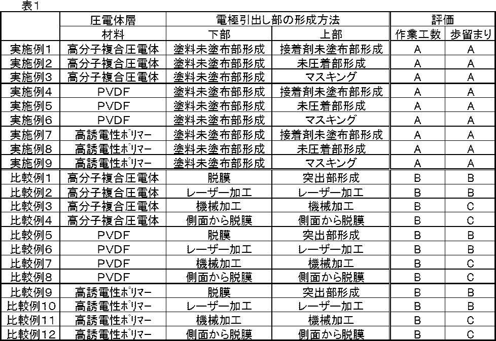
表1より、本発明の製造方法である実施例1~9は、圧電体層と電極積層体とを積層する際に、電極引出し部となる未接着部を設けるので、電極引出し部を形成することのみを目的とした工程を有する必要がなく、比較例1~12に比べて、作業工数が少なくなる。
したがって、コストを削減できる。
また、本発明の製造方法である実施例1~9で作製した変換フィルム原反は、圧電体層と電極積層体とを積層する際に、電極引出し部となる未接着部を設けるので、薄膜電極を傷つけることなく、比較例1~12に比べて、歩留まりを向上できる。
以上の結果より、本発明の効果は、明らかである。
したがって、コストを削減できる。
また、本発明の製造方法である実施例1~9で作製した変換フィルム原反は、圧電体層と電極積層体とを積層する際に、電極引出し部となる未接着部を設けるので、薄膜電極を傷つけることなく、比較例1~12に比べて、歩留まりを向上できる。
以上の結果より、本発明の効果は、明らかである。
10、10b 電気音響変換フィルム原反
11a 下部電極積層体
11b 積層体
11c 上部電極積層体
12 圧電体層
12a 上面
14、14b 下部薄膜電極
15、17 接着剤層
16 上部薄膜電極
18、18b 下部保護層
20 上部保護層
24 マトリックス
26 圧電体粒子
30 コロナ電極
32 直流電源
36 配線
40 圧電スピーカ
42 ケース
44 電気音響変換フィルム
46 弾性支持体
48 枠体
11a 下部電極積層体
11b 積層体
11c 上部電極積層体
12 圧電体層
12a 上面
14、14b 下部薄膜電極
15、17 接着剤層
16 上部薄膜電極
18、18b 下部保護層
20 上部保護層
24 マトリックス
26 圧電体粒子
30 コロナ電極
32 直流電源
36 配線
40 圧電スピーカ
42 ケース
44 電気音響変換フィルム
46 弾性支持体
48 枠体
Claims (19)
- 誘電性を有する圧電体層、前記圧電体層の両面にそれぞれ形成される2つの薄膜電極と、2つの前記薄膜電極上それぞれに形成される2つの保護層と、を有する電気音響変換フィルム原反の製造方法であって、
1つの前記薄膜電極と1つの前記保護層とが積層されてなる電極積層体を準備する準備工程、および、
前記電極積層体と、前記圧電体層とを積層する積層工程を有し、
前記積層工程において、前記電極積層体と前記圧電体層とを積層する際に、前記薄膜電極の少なくとも1つの端部に前記圧電体層と接着されない未接着部を設けることを特徴とする電気音響変換フィルム原反の製造方法。 - 前記積層工程は、前記電極積層体の前記薄膜電極上に、前記圧電体層となる塗布組成物を塗布した後、硬化して前記圧電体層を形成して、前記電極積層体と前記圧電体層とを積層する第1積層工程であり、
第1積層工程において、前記塗布組成物を塗布する際に、前記薄膜電極の前記少なくとも1つの端部を、前記塗布組成物の塗布を行わない塗料未塗布部とすることで、前記未接着部を形成する請求項1に記載の電気音響変換フィルム原反の製造方法。 - 前記積層工程は、前記圧電体層と、前記電極積層体の前記薄膜電極側とを貼り合わせて、前記電極積層体と前記圧電体層とを積層する第2積層工程であり、
前記第2積層工程において、前記薄膜電極の前記少なくとも1つの端部を、前記圧電体層と貼り合わせない未貼合部とすることで、前記未接着部を形成する請求項1に記載の電気音響変換フィルム原反の製造方法。 - 前記準備工程は、大きさの異なる2つの前記電極積層体を準備する工程であり、
前記積層工程として、
大きい方の前記電極積層体の前記薄膜電極上に、前記圧電体層となる塗布組成物を塗布した後、硬化して前記圧電体層を形成して、大きい方の前記電極積層体と前記圧電体層とを積層する第1積層工程と、
大きい方の前記電極積層体と積層された前記圧電体層の、大きい方の前記電極積層体が積層された面とは反対側の面に、小さい方の前記電極積層体の前記薄膜電極側を貼り合わせて、小さい方の前記電極積層体と前記圧電体層とを積層する第2積層工程と、を有し、
前記第1積層工程において、前記塗布組成物を塗布する際に、前記薄膜電極の前記少なくとも1つの端部を、前記塗布組成物の塗布を行わない塗料未塗布部とすることで、前記未接着部を形成し、
前記第2積層工程において、前記薄膜電極の前記少なくとも1つの端部を、前記圧電体層と貼り合わせない未貼合部とすることで、前記未接着部を形成する請求項1に記載の電気音響変換フィルム原反の製造方法。 - 前記第2積層工程は、前記電極積層体の前記薄膜電極側に、接着剤を塗布する接着剤塗布工程と、前記接着剤を介して前記圧電体層と前記電極積層体とを貼り合わせる貼合工程とを有し、
前記接着剤塗布工程において、前記薄膜電極の前記少なくとも1つの端部を、前記接着剤の塗布を行わない接着剤未塗布部とすることで、前記未接着部を形成する請求項3または4に記載の電気音響変換フィルム原反の製造方法。 - 前記第2積層工程は、前記圧電体層と前記電極積層体とを圧着して貼り合わせるものであり、
前記薄膜電極の前記少なくとも1つの端部を、前記圧電体層と圧着しない未圧着部とすることで、前記未接着部を形成する請求項3~5のいずれか1項に記載の電気音響変換フィルム原反の製造方法。 - 前記第2積層工程において、前記薄膜電極の前記少なくとも1つの端部をマスキングして、前記圧電体層と前記電極積層体とを貼り合わせることで、前記未接着部を形成する請求項3~6のいずれか1項に記載の電気音響変換フィルム原反の製造方法。
- 前記第2積層工程において前記圧電体層に積層される前記薄膜電極の、前記圧電体層の主面に垂直な方向から見た際の面積が、前記圧電体層の面積よりも小さい請求項3~7のいずれか1項に記載の電気音響変換フィルム原反の製造方法。
- 前記未接着部の幅が、5~20mmである請求項1~8のいずれか1項に記載の電気音響変換フィルム原反の製造方法。
- 前記薄膜電極の主面の形状が四角形状であり、前記薄膜電極の対向する2辺それぞれの側の端部を前記未接着部とする請求項1~9のいずれか1項に記載の電気音響変換フィルム原反の製造方法。
- 前記電極積層体の厚さが、4~20μmである請求項1~10のいずれか1項に記載の電気音響変換フィルム原反の製造方法。
- 前記圧電体層が、常温で粘弾性を有する高分子材料からなる粘弾性マトリックス中に圧電体粒子を分散してなる高分子複合圧電体である請求項1~11のいずれか1項に記載の電気音響変換フィルム原反の製造方法。
- 前記高分子材料の動的粘弾性測定による周波数1Hzでの損失正接Tanδが0.5以上となる極大値が0~50℃の温度範囲に存在する請求項12に記載の電気音響変換フィルム原反の製造方法。
- 前記高分子材料が、シアノエチル基を有するものである請求項12または13に記載の電気音響変換フィルム原反の製造方法。
- 前記高分子材料が、シアノエチル化ポリビニルアルコールである請求項12~14のいずれか1項に記載の電気音響変換フィルム原反の製造方法。
- 請求項1~15のいずれか1項に記載の電気音響変換フィルム原反の製造方法で作製された電気音響変換フィルム原反を、所定の形状に切断する切断工程を有し、
前記切断工程において、前記薄膜電極の未接着部の少なくとも一部を残す形状に切断する電気音響変換フィルムの製造方法。 - 誘電性を有する圧電体層と、前記圧電体層の一方の主面に形成される上部薄膜電極と、前記圧電体層の他方の主面に形成される下部薄膜電極と、前記上部薄膜電極上に形成される上部保護層と、前記下部薄膜電極上に形成される下部保護層とを有する電気音響変換フィルム原反であって、
前記圧電体層の主面に垂直な方向から見た際の、前記下部薄膜電極の面積が、前記圧電体層の面積よりも大きく、かつ、前記下部薄膜電極の少なくとも1つの端部に、前記圧電体層が積層されていない未接着部を有し、
前記圧電体層の主面に垂直な方向から見た際の、前記上部薄膜電極の面積が、前記圧電体層の面積よりも小さく、かつ、前記上部薄膜電極の少なくとも1つの端部に、前記圧電体層と接着されていない未接着部を有することを特徴とする電気音響変換フィルム原反。 - 誘電性を有する圧電体層と、前記圧電体層の両面にそれぞれ形成される2つの薄膜電極と、2つの前記薄膜電極上それぞれに形成される2つの保護層とを有する電気音響変換フィルム原反であって、
前記圧電体層の主面に垂直な方向から見た際の、2つの前記薄膜電極それぞれの面積が、前記圧電体層の面積よりも小さく、かつ、前記薄膜電極それぞれの少なくとも1つの端部に、前記圧電体層と接着されていない未接着部を有することを特徴とする電気音響変換フィルム原反。 - 誘電性を有する圧電体層と、前記圧電体層の両面にそれぞれ形成される2つの薄膜電極と、2つの前記薄膜電極上それぞれに形成される2つの保護層とを有する電気音響変換フィルムであって、
前記圧電体層、2つの前記薄膜電極、および、2つの前記保護層が、同一形状で、かつ、互いに接着された領域と、
前記圧電体層、2つの前記薄膜電極、および、2つの前記保護層が、積層方向に互いに重複し、かつ、前記圧電体層と2つの前記薄膜電極とが互いに接着されない領域とを有することを特徴とする電気音響変換フィルム。
Priority Applications (3)
| Application Number | Priority Date | Filing Date | Title |
|---|---|---|---|
| JP2017517953A JP6261820B2 (ja) | 2015-05-11 | 2016-05-10 | 電気音響変換フィルム原反、電気音響変換フィルム、および、その製造方法 |
| US15/808,108 US10224477B2 (en) | 2015-05-11 | 2017-11-09 | Electroacoustic conversion film web, electroacoustic conversion film, and method of manufacturing an electroacoustic conversion film web |
| US16/254,192 US10770647B2 (en) | 2015-05-11 | 2019-01-22 | Electroacoustic conversion film web, electroacoustic conversion film, and method of manufacturing an electroacoustic conversion film web |
Applications Claiming Priority (2)
| Application Number | Priority Date | Filing Date | Title |
|---|---|---|---|
| JP2015-096470 | 2015-05-11 | ||
| JP2015096470 | 2015-05-11 |
Related Child Applications (1)
| Application Number | Title | Priority Date | Filing Date |
|---|---|---|---|
| US15/808,108 Continuation US10224477B2 (en) | 2015-05-11 | 2017-11-09 | Electroacoustic conversion film web, electroacoustic conversion film, and method of manufacturing an electroacoustic conversion film web |
Publications (1)
| Publication Number | Publication Date |
|---|---|
| WO2016181965A1 true WO2016181965A1 (ja) | 2016-11-17 |
Family
ID=57247963
Family Applications (1)
| Application Number | Title | Priority Date | Filing Date |
|---|---|---|---|
| PCT/JP2016/063883 Ceased WO2016181965A1 (ja) | 2015-05-11 | 2016-05-10 | 電気音響変換フィルム原反、電気音響変換フィルム、および、その製造方法 |
Country Status (3)
| Country | Link |
|---|---|
| US (2) | US10224477B2 (ja) |
| JP (1) | JP6261820B2 (ja) |
| WO (1) | WO2016181965A1 (ja) |
Cited By (4)
| Publication number | Priority date | Publication date | Assignee | Title |
|---|---|---|---|---|
| WO2019181407A1 (ja) * | 2018-03-22 | 2019-09-26 | 株式会社東海理化電機製作所 | 圧電素子及び触覚呈示装置 |
| WO2021095461A1 (ja) | 2019-11-12 | 2021-05-20 | 富士フイルム株式会社 | 圧電素子 |
| JPWO2021095511A1 (ja) * | 2019-11-12 | 2021-05-20 | ||
| JP2024059951A (ja) * | 2021-07-30 | 2024-05-01 | エルジー ディスプレイ カンパニー リミテッド | 振動装置および装置 |
Families Citing this family (7)
| Publication number | Priority date | Publication date | Assignee | Title |
|---|---|---|---|---|
| US11359693B2 (en) * | 2017-11-09 | 2022-06-14 | Magnecomp Corporation | Pseudo feature configured as a damper for a disk-drive suspension |
| US11337008B2 (en) | 2017-12-07 | 2022-05-17 | Sony Group Corporation | Display panel and display apparatus |
| EP3876307B1 (en) * | 2018-11-09 | 2024-07-10 | Shenzhen Yuanzi Technology Co., Ltd. | Film preparation process |
| CN114009062A (zh) | 2019-06-28 | 2022-02-01 | 富士胶片株式会社 | 压电薄膜 |
| GB2588218B (en) * | 2019-10-17 | 2021-10-27 | Darkvision Tech Ltd | Acoustic transducer and method of manufacturing |
| CN111447541A (zh) * | 2019-12-26 | 2020-07-24 | 瑞声科技(新加坡)有限公司 | 一种碳纤维球顶的制造方法 |
| CN112565983A (zh) * | 2020-11-02 | 2021-03-26 | 歌尔股份有限公司 | 用于发声装置的振膜及发声装置 |
Citations (2)
| Publication number | Priority date | Publication date | Assignee | Title |
|---|---|---|---|---|
| JPS5773512A (en) * | 1980-10-27 | 1982-05-08 | Mitsubishi Electric Corp | Piezoelectric oscillator |
| JP2014014063A (ja) * | 2011-09-30 | 2014-01-23 | Fujifilm Corp | 電気音響変換フィルム、フレキシブルディスプレイ、声帯マイクロフォンおよび楽器用センサー |
Family Cites Families (7)
| Publication number | Priority date | Publication date | Assignee | Title |
|---|---|---|---|---|
| US7019621B2 (en) * | 2001-01-02 | 2006-03-28 | Stanley E. Woodard | Methods and apparatus to increase sound quality of piezoelectric devices |
| JP2004356700A (ja) * | 2003-05-27 | 2004-12-16 | Murata Mfg Co Ltd | 圧電共振子の製造方法、ならびに圧電共振子、圧電フィルタ、およびデュプレクサ |
| JP4960765B2 (ja) | 2007-05-22 | 2012-06-27 | 日本放送協会 | フレキシブルスピーカの音質補正装置および音質補正装置を備えたスピーカシステム |
| JP6005093B2 (ja) * | 2013-03-28 | 2016-10-12 | 富士フイルム株式会社 | 電気音響変換フィルム、電気音響変換器、フレキシブルディスプレイおよびプロジェクター用スクリーン |
| WO2014157684A1 (ja) * | 2013-03-29 | 2014-10-02 | 富士フイルム株式会社 | スピーカシステム |
| JP6005089B2 (ja) * | 2013-03-29 | 2016-10-12 | 富士フイルム株式会社 | 電気音響変換フィルム |
| JP6216884B2 (ja) * | 2014-06-30 | 2017-10-18 | 富士フイルム株式会社 | 電気音響変換フィルムおよびデジタルスピーカ |
-
2016
- 2016-05-10 JP JP2017517953A patent/JP6261820B2/ja not_active Expired - Fee Related
- 2016-05-10 WO PCT/JP2016/063883 patent/WO2016181965A1/ja not_active Ceased
-
2017
- 2017-11-09 US US15/808,108 patent/US10224477B2/en active Active
-
2019
- 2019-01-22 US US16/254,192 patent/US10770647B2/en active Active
Patent Citations (2)
| Publication number | Priority date | Publication date | Assignee | Title |
|---|---|---|---|---|
| JPS5773512A (en) * | 1980-10-27 | 1982-05-08 | Mitsubishi Electric Corp | Piezoelectric oscillator |
| JP2014014063A (ja) * | 2011-09-30 | 2014-01-23 | Fujifilm Corp | 電気音響変換フィルム、フレキシブルディスプレイ、声帯マイクロフォンおよび楽器用センサー |
Cited By (12)
| Publication number | Priority date | Publication date | Assignee | Title |
|---|---|---|---|---|
| WO2019181407A1 (ja) * | 2018-03-22 | 2019-09-26 | 株式会社東海理化電機製作所 | 圧電素子及び触覚呈示装置 |
| WO2021095461A1 (ja) | 2019-11-12 | 2021-05-20 | 富士フイルム株式会社 | 圧電素子 |
| JPWO2021095511A1 (ja) * | 2019-11-12 | 2021-05-20 | ||
| WO2021095511A1 (ja) * | 2019-11-12 | 2021-05-20 | 富士フイルム株式会社 | 圧電素子 |
| JPWO2021095461A1 (ja) * | 2019-11-12 | 2021-05-20 | ||
| KR20220076506A (ko) | 2019-11-12 | 2022-06-08 | 후지필름 가부시키가이샤 | 압전 소자 |
| CN114730827A (zh) * | 2019-11-12 | 2022-07-08 | 富士胶片株式会社 | 压电元件 |
| JP7259075B2 (ja) | 2019-11-12 | 2023-04-17 | 富士フイルム株式会社 | 圧電素子 |
| JP7286790B2 (ja) | 2019-11-12 | 2023-06-05 | 富士フイルム株式会社 | 圧電素子 |
| US11895463B2 (en) | 2019-11-12 | 2024-02-06 | Fujifilm Corporation | Piezoelectric element |
| JP2024059951A (ja) * | 2021-07-30 | 2024-05-01 | エルジー ディスプレイ カンパニー リミテッド | 振動装置および装置 |
| JP7793668B2 (ja) | 2021-07-30 | 2026-01-05 | エルジー ディスプレイ カンパニー リミテッド | 振動装置および装置 |
Also Published As
| Publication number | Publication date |
|---|---|
| US20180069172A1 (en) | 2018-03-08 |
| JPWO2016181965A1 (ja) | 2018-02-15 |
| US10224477B2 (en) | 2019-03-05 |
| JP6261820B2 (ja) | 2018-01-17 |
| US20190157543A1 (en) | 2019-05-23 |
| US10770647B2 (en) | 2020-09-08 |
Similar Documents
| Publication | Publication Date | Title |
|---|---|---|
| JP6261820B2 (ja) | 電気音響変換フィルム原反、電気音響変換フィルム、および、その製造方法 | |
| JP6297204B2 (ja) | 高分子複合圧電体、電気音響変換フィルムおよび電気音響変換器 | |
| JP6071932B2 (ja) | 電気音響変換フィルム | |
| JP6196400B2 (ja) | 電気音響変換フィルム | |
| WO2020196850A1 (ja) | 圧電フィルム、積層圧電素子および電気音響変換器 | |
| JP7390390B2 (ja) | 圧電フィルムおよび圧電フィルムの製造方法 | |
| JP5993772B2 (ja) | 電気音響変換フィルム、フレキシブルディスプレイ、声帯マイクロフォンおよび楽器用センサー | |
| WO2020261963A1 (ja) | 高分子複合圧電体および圧電フィルム | |
| JP7355819B2 (ja) | 圧電フィルム | |
| WO2014157684A1 (ja) | スピーカシステム | |
| WO2020261954A1 (ja) | 電気音響変換フィルムおよび電気音響変換器 | |
| WO2020261911A1 (ja) | 高分子複合圧電体、圧電フィルム、圧電スピーカー、フレキシブルディスプレイ | |
| WO2021157288A1 (ja) | 圧電フィルム | |
| JP6505845B2 (ja) | 電気音響変換フィルム | |
| JP6450014B2 (ja) | 電気音響変換フィルム、電気音響変換フィルムの製造方法および電気音響変換器 | |
| JP6193194B2 (ja) | 電気音響変換フィルムおよび電気音響変換器 | |
| WO2016017632A1 (ja) | 電気音響変換フィルムおよび電気音響変換器 | |
| CN117813841A (zh) | 压电膜及压电元件 | |
| WO2016136522A1 (ja) | 構造体および電気音響変換器 | |
| WO2021124743A1 (ja) | 圧電フィルム | |
| WO2021095461A1 (ja) | 圧電素子 | |
| JP6297223B2 (ja) | 電気音響変換フィルムおよび電気音響変換器 | |
| WO2023188929A1 (ja) | 圧電フィルム、圧電素子、および、電気音響変換器 | |
| WO2023188966A1 (ja) | 圧電フィルム、圧電素子、および、電気音響変換器 |
Legal Events
| Date | Code | Title | Description |
|---|---|---|---|
| 121 | Ep: the epo has been informed by wipo that ep was designated in this application |
Ref document number: 16792690 Country of ref document: EP Kind code of ref document: A1 |
|
| ENP | Entry into the national phase |
Ref document number: 2017517953 Country of ref document: JP Kind code of ref document: A |
|
| NENP | Non-entry into the national phase |
Ref country code: DE |
|
| 122 | Ep: pct application non-entry in european phase |
Ref document number: 16792690 Country of ref document: EP Kind code of ref document: A1 |