WO2016185837A1 - 熱抵抗解析モデル、および半導体集積回路 - Google Patents
熱抵抗解析モデル、および半導体集積回路 Download PDFInfo
- Publication number
- WO2016185837A1 WO2016185837A1 PCT/JP2016/061898 JP2016061898W WO2016185837A1 WO 2016185837 A1 WO2016185837 A1 WO 2016185837A1 JP 2016061898 W JP2016061898 W JP 2016061898W WO 2016185837 A1 WO2016185837 A1 WO 2016185837A1
- Authority
- WO
- WIPO (PCT)
- Prior art keywords
- node
- thermal resistance
- analysis model
- semiconductor chip
- integrated circuit
- Prior art date
- Legal status (The legal status is an assumption and is not a legal conclusion. Google has not performed a legal analysis and makes no representation as to the accuracy of the status listed.)
- Ceased
Links
Images






Classifications
-
- G—PHYSICS
- G06—COMPUTING OR CALCULATING; COUNTING
- G06F—ELECTRIC DIGITAL DATA PROCESSING
- G06F30/00—Computer-aided design [CAD]
- G06F30/20—Design optimisation, verification or simulation
- G06F30/22—Design optimisation, verification or simulation using Petri net models
-
- G—PHYSICS
- G06—COMPUTING OR CALCULATING; COUNTING
- G06F—ELECTRIC DIGITAL DATA PROCESSING
- G06F30/00—Computer-aided design [CAD]
-
- G—PHYSICS
- G06—COMPUTING OR CALCULATING; COUNTING
- G06F—ELECTRIC DIGITAL DATA PROCESSING
- G06F30/00—Computer-aided design [CAD]
- G06F30/30—Circuit design
- G06F30/36—Circuit design at the analogue level
- G06F30/367—Design verification, e.g. using simulation, simulation program with integrated circuit emphasis [SPICE], direct methods or relaxation methods
-
- G—PHYSICS
- G06—COMPUTING OR CALCULATING; COUNTING
- G06F—ELECTRIC DIGITAL DATA PROCESSING
- G06F30/00—Computer-aided design [CAD]
- G06F30/30—Circuit design
- G06F30/39—Circuit design at the physical level
- G06F30/398—Design verification or optimisation, e.g. using design rule check [DRC], layout versus schematics [LVS] or finite element methods [FEM]
-
- H—ELECTRICITY
- H10—SEMICONDUCTOR DEVICES; ELECTRIC SOLID-STATE DEVICES NOT OTHERWISE PROVIDED FOR
- H10W—GENERIC PACKAGES, INTERCONNECTIONS, CONNECTORS OR OTHER CONSTRUCTIONAL DETAILS OF DEVICES COVERED BY CLASS H10
- H10W72/00—Interconnections or connectors in packages
-
- G—PHYSICS
- G06—COMPUTING OR CALCULATING; COUNTING
- G06F—ELECTRIC DIGITAL DATA PROCESSING
- G06F2113/00—Details relating to the application field
- G06F2113/18—Chip packaging
-
- G—PHYSICS
- G06—COMPUTING OR CALCULATING; COUNTING
- G06F—ELECTRIC DIGITAL DATA PROCESSING
- G06F2119/00—Details relating to the type or aim of the analysis or the optimisation
- G06F2119/08—Thermal analysis or thermal optimisation
Definitions
- This embodiment relates to a thermal resistance analysis model and a semiconductor integrated circuit.
- the ambient temperature Ta of the device is greatly influenced by the arrangement of each heat generating component on the mounting substrate.
- CFD computational Fluid Dynamics
- This embodiment provides a highly accurate thermal resistance analysis model as a thermal resistance analysis model of a semiconductor integrated circuit that generates local heat, and a semiconductor integrated circuit to which this thermal resistance analysis model is applied.
- a die that constitutes a bottom inner node, and a semiconductor chip that is disposed on the die and has a local heat generating portion that constitutes a junction node, and that constitutes an additional plate node.
- the semiconductor integrated circuit includes a first thermal resistance between the junction node and the plate node, and a second thermal resistance between the plate node and the bottom inner node, and the semiconductor integrated circuit is represented by a multi-thermal resistance network.
- a thermal resistance analysis model is provided.
- the die constituting the bottom inner node, the first local heat generating part arranged on the die and constituting the first junction node, and the first local heat generating part are separated from each other.
- a thermal resistance analysis model that has four thermal resistances and represents the semiconductor integrated circuit with a multi-thermal resistance network It is.
- a semiconductor integrated circuit to which the above thermal resistance analysis model is applied is provided.
- thermo resistance analysis model as a thermal resistance analysis model of a semiconductor integrated circuit that locally generates heat, and a semiconductor integrated circuit to which this thermal resistance analysis model is applied.
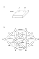
- FIG. 1 is a bird's-eye view of a semiconductor integrated circuit to which a thermal resistance analysis model according to a first embodiment is applied.
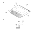
- the semiconductor integrated circuit to which the thermal resistance analysis model according to the first embodiment is applied (a) an explanatory diagram of a top inner TI, a top outer TO, a side SI, and a lead LE, and (b) a lead side LES of the lead LE and Explanatory drawing of lead foot LEF.
- FIG. 1 An explanatory view of the shape of a detailed model (no standard) as a CFD applied thermal resistance analysis model according to a comparative example.
- a numerical example of the junction temperature and thermal resistance ⁇ JA of the semiconductor chip when the entire surface is heated calculated using a detailed model.
- a numerical example of the junction temperature and thermal resistance ⁇ JA of the semiconductor chip when the entire surface is heated calculated by applying the DELPHI model.
- a numerical example of the junction temperature and thermal resistance ⁇ JA of a semiconductor chip during local heat generation calculated by applying a detailed model.
- a numerical example of the junction temperature and thermal resistance ⁇ JA of a semiconductor chip at the time of local heat generation calculated by applying the DELPHI model As a comparative example, a numerical example of the junction temperature and thermal resistance ⁇ JA of a semiconductor chip at the time of local heat generation calculated by applying the DELPHI model.
- A As a comparative example, a bird's-eye view of a semiconductor chip when the entire surface heat is applied to which the DELPHI model is applied, and (b) an explanatory diagram of the shape of the DELPHI model corresponding to FIG.
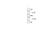
- FIG. 3 is an explanatory diagram of a shape between a junction node JN and a bottom inner node BI in a local DELPHI model to which a plate node PN is added as a thermal resistance analysis model according to the first embodiment.
- the bird's-eye view block diagram of the semiconductor integrated circuit which applies the local DELPHI model which added the plate node PN as a thermal resistance analysis model which concerns on 1st Embodiment.
- (A) In the semiconductor integrated circuit to which the thermal resistance analysis model according to the first embodiment is applied, a schematic diagram in a cross-sectional direction of the semiconductor chip 10 (PN) for explaining a state where an isothermal line ET is drawn from the junction node JN.
- (B) In the semiconductor integrated circuit corresponding to FIG. 14 to which the thermal resistance analysis model according to the first embodiment is applied, a schematic top view of a semiconductor chip for explaining a state in which an isotherm is drawn from the junction node JN. The thermal resistance analysis result of each part of the semiconductor integrated circuit to which the local DELPHI model is applied as the thermal resistance analysis model according to the first embodiment.
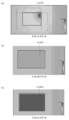
- FIG. 20 are substrate specifications, (a) a schematic cross-sectional structure diagram of a 1s (one layer) substrate, (b) a schematic cross-sectional structure diagram of a 2s (two-layer) substrate, and (c) a 2s2p (four-layer) substrate.
- FIG. FIG. 3 is an explanatory diagram of a semiconductor integrated circuit that considers heat dissipation in the upper surface direction of the semiconductor integrated circuit during local heat generation in the local DELPHI model as a thermal resistance analysis model according to the first embodiment.
- FIG. 5 is an explanatory diagram of a shape portion of a local DELPHI model expressing a plurality of local heat generations.
- A A schematic plan view of an integrated circuit for system power supply to which a local DELPHI model expressing a plurality of local heat generations is applied as a thermal resistance analysis model according to the second embodiment, and (b) in FIG.
- the bird's-eye view of the semiconductor integrated circuit to which the local DELPHI model expressing (A) Schematic plan view of a semiconductor chip to which a local DELPHI model is applied when it has three junction nodes as a thermal resistance analysis model according to the third embodiment, and (b) a third embodiment.
- the top inner node TI may be simply expressed as a top inner TI.
- a bird's-eye view configuration example of the semiconductor integrated circuit 100 to which the thermal resistance analysis model according to the first embodiment is applied is expressed as shown in FIG.
- a semiconductor (LSI) chip can be mounted in the semiconductor integrated circuit 100.
- the description of each part of the top inner TI, the top outer TO, the side SI, and the lead LE is as shown in FIG. Is done.
- the description of each part of the lead foot LEF and the lead side LES of the lead LE is expressed as shown in FIG.
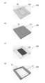
- each part of the bottom inner BI and the bottom outer BO is described as shown in FIG.
- the description of each part of the top outer TO is expressed as shown in FIG.
- the description of the junction node JN is expressed as shown in FIG.
- the description of the side SI and lead LE portions is expressed as shown in FIG.
- the CFD applied thermal resistance analysis model according to the comparative example can be selected from three models, a detailed model, a DELPHI model, and a two resistance model, depending on the purpose of the analysis.
- the detailed model models the internal structure in as much detail as possible while simplifying it using the fact that it is thermally equivalent.
- the 2-resistance model is generally the simplest form, and the shape is simply modeled as two thermal resistances.
- the DELPHI model is a more detailed thermal resistance model than the two-resistance model modeled with six or more thermal resistances.
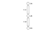
- the description of the shape of the 2-resistance compact model (JESD15-3) is expressed as shown in FIG.
- the shape of the two-resistance compact model (JESD15-3) includes a simple model in which the semiconductor integrated circuit 100 is simply divided up and down from the junction node JN.
- the two-resistance compact model (JESD15-3) includes a junction node JN, a case node CN, a board node BN, and a thermal resistance ⁇ JC arranged between the junction node JN and the case node CN.
- junction node JN corresponds to a junction portion serving as a heat source of the semiconductor chip.
- case node CN corresponds to a case portion arranged upward from the junction node JN.
- board node BN corresponds to a mounting substrate portion on which a semiconductor chip is mounted.
- the 2-resistance compact model (JESD15-3) has a junction node JN composed of one node. Moreover, the accuracy as the heat generation model is low.
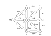
- the shape of the DELPHI compact model (JESD15-4) includes a model in which a semiconductor integrated circuit is expressed by a multi-heat resistance network, as shown in FIG. That is, as shown in FIG. 5, the DELPHI compact model (JESD15-4) includes a junction node JN, a top inner node TI, a top outer node TO, a bottom inner node BI, a bottom outer node BO, and a side node.
- thermal resistance ⁇ JTI disposed between junction node JN and top inner node TI
- thermal resistance ⁇ JTO disposed between junction node JN and top outer node TO
- junction node JN side node Thermal resistance ⁇ JS disposed between SI, thermal resistance ⁇ JL disposed between junction node JN and lead node LE, thermal resistance ⁇ JBI disposed between junction node JN and bottom inner node BI, and junction node JN Bottom out
- the thermal resistance ⁇ JBO disposed between the node BO and the top inner node TI and the top outer node TO, the thermal resistance ⁇ TS disposed between the top inner node TI and the side node SI, and the top Thermal resistance ⁇ TL arranged between outer node TO and lead node LE, thermal resistance ⁇ S B arranged between side node SI and bottom inner node BI, and heat arranged between lead node LE and bottom outer node BO
- a resistance ⁇ LB and a thermal resistance ⁇ BIO disposed between the bottom inner node BI and the
- the bottom inner node BI and the bottom outer node BO correspond to the inner portion and the outer portion of the mounting substrate portion on which the semiconductor chip is mounted in the semiconductor integrated circuit.
- the top inner node TI and the top outer node TO are, as shown in FIGS. 2A and 3B, an inner portion and an outer portion of the upper case portion in which the semiconductor chip is disposed. It corresponds to.
- the junction node JN corresponds to a junction portion that becomes a heat source of the semiconductor chip in the semiconductor integrated circuit.
- the side node SI and the lead node LE are provided in the side portion of the case portion on which the semiconductor chip is mounted and the lead terminal arrangement portion in the semiconductor integrated circuit. It corresponds.
- the DELPHI compact model (JESD15-4) has a junction node JN composed of one node. Further, the accuracy as the heat generation model is good, but it is difficult to cope with local heat generation.
- the description of the shape of the detailed model (no standard) of the semiconductor integrated circuit 100M is expressed as shown in FIG. That is, the detailed model is a model with a low abstraction level because it includes the semiconductor chip constituting the semiconductor integrated circuit 100M, the dimensions and physical property values of each component, and the like.
- the accuracy of the detailed model is the best as the heat generation model, but it is difficult to obtain in practice because it contains internal detailed information, and there is no standard, and the quality is different for each company.
- calculation time is required and compatibility between analysis tools is low.
- the detailed model according to the comparative example has difficulty in availability. Further, the two-resistance model according to the comparative example cannot be used for detailed design. On the other hand, the DELPHI model according to the comparative example is realistic, but it is difficult to cope with local heat generation.
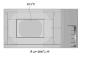
- junction temperature 82.5 ° C.
- thermal resistance ⁇ JA 20.6 ° C./W.
- junction temperature 82.6 ° C.
- thermal resistance ⁇ JA 20.7 ° C./W.
- the calculation result of the junction temperature and thermal resistance ⁇ JA of the semiconductor chip during the entire surface heat generation calculated by applying the DELPHI model is substantially the same as the calculation result of the detailed model. The accuracy is good.
- FIG. 9 a numerical example of the junction temperature and the thermal resistance ⁇ JA of the semiconductor chip during local heat generation calculated by applying a detailed model is expressed as shown in FIG.
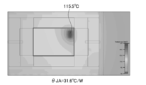
- the maximum junction temperature is 115.5 ° C.
- the thermal resistance ⁇ JA is 31.6 ° C./W.
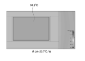
- junction temperature 91.9 ° C.
- thermal resistance ⁇ JA 23.7 ° C./W.
- the calculation results of the semiconductor chip junction temperature and thermal resistance ⁇ JA during local heat generation calculated using the DELPHI model show significantly different values from the detailed model calculation results.
- the accuracy as a heat generation model is low.
- the DELPHI model does not support local heat generation.
- FIG. 11A the bird's-eye view configuration of the semiconductor chip 10 during the entire surface heat generation to which the DELPHI model is applied is represented as shown in FIG. 11A, and the description of the DELPHI model shape corresponding to FIG. It is expressed as shown in (b).
- FIG. 11A in the semiconductor chip 10 in the entire surface heat generation to which the DELPHI model is applied, the entire semiconductor chip 10 is represented as the junction node JN itself.
- FIG. 11B for explaining the shape of the DELPHI model corresponding to FIG. 11A is similar to the shape of the DELPHI compact model (JESD15-4) shown in FIG. Since the model expressed by is provided, redundant description is omitted.
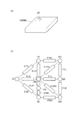
- FIG. 12A The bird's-eye view configuration of the semiconductor chip 10 to which the local DELPHI model is applied as the thermal resistance analysis model according to the first embodiment is expressed as shown in FIG. 12A and corresponds to the local DELPHI corresponding to FIG.
- the description of the shape of the model is expressed as shown in FIG.
- a local DELPHI model expressing local heat generation in the semiconductor chip 10 can be provided by adding one plate node PN. That is, in the thermal resistance analysis model according to the first embodiment, as shown in FIG. 12A, in the semiconductor chip 10, a local heat generating part in a junction part such as a power transistor is expressed by a junction node JN. A portion of the semiconductor chip 10 other than the local heat generating portion is expressed by a plate node PN.
- the shape of the local DELPHI model includes a model in which a semiconductor integrated circuit is represented by a multi-thermal resistance network, as shown in FIG.
- the local DELPHI model as the thermal resistance analysis model according to the first embodiment includes a junction node JN, an added plate node PN, a top inner node TI, as shown in FIG. Top outer node TO, bottom inner node BI, bottom outer node BO, side node SI, lead node LE, thermal resistance ⁇ JTI disposed between junction node JN and top inner node TI, and junction node JN Thermal resistance ⁇ JTO disposed between the top outer node TO, thermal resistance ⁇ JS disposed between the junction node JN and the side node SI, thermal resistance ⁇ JL disposed between the junction node JN and the lead node LE, and a junction node Arranged between JN and plate node PN Thermal resistance ⁇ JP, thermal resistance ⁇ PBI disposed between plate node PN and bottom inner node BI, thermal resistance ⁇ JBO disposed between junction node JN and bottom outer node BO, top inner node TI and top outer node Thermal resistance ⁇ TIO disposed between
- bottom inner node BI and the bottom outer node BO correspond to the inner portion and the outer portion of the mounting substrate portion on which the semiconductor chip 10 is mounted in the semiconductor integrated circuit, as in FIG.
- top inner node TI and the top outer node TO are, as in FIGS. 2 (a) and 3 (b), an inner portion and an outer portion of the upper surface case portion where the semiconductor chip 10 is disposed in the semiconductor integrated circuit. It corresponds to.
- the junction node JN corresponds to a junction portion that becomes a local heat source of the semiconductor chip 10 in the semiconductor integrated circuit.
- the additional plate node PN corresponds to the semiconductor chip 10 (PN) other than the junction node JN that becomes a local heat source of the semiconductor chip 10 in the semiconductor integrated circuit, as shown in FIG. Yes.
- the side node SI and the lead node LE are provided in the side portion of the case portion on which the semiconductor chip 10 is mounted and the lead terminal arrangement portion in the semiconductor integrated circuit. It corresponds.
- the local DELPHI model as the thermal resistance analysis model according to the first embodiment, one plate node PN is added, the local heat generation part is expressed by the junction node JN, and the semiconductor chip 10 other than the local heat generation part is represented.
- the plate node PN By expressing the plate node PN, local heat generation in the chip can be expressed with high accuracy.
- FIG. 13 is an extraction of the broken line portion of FIG.
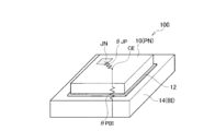
- the bird's-eye view configuration of the semiconductor integrated circuit 100 to which the local DELPHI model to which the plate node PN is added is applied as the thermal resistance analysis model according to the first embodiment is expressed as shown in FIG.
- the semiconductor integrated circuit 100 to which the local DELPHI model is applied as a thermal resistance analysis model includes a die 14, a die connection unit 12, and a semiconductor chip 10.
- the semiconductor chip 10 is disposed on the die 14 via the die connection part 12.
- the die 14 constitutes an island such as a metal layer mounted on the substrate, and corresponds to the bottom inner node BI in the local DELPHI model.
- the die connection part 12 is composed of a solder layer or the like that connects the die 14 and the semiconductor chip 10.
- the local heat generating part of the semiconductor chip 10 is represented by a junction node JN.
- the semiconductor chip 10 portion other than the local heat generating portion (junction node JN) is represented by a plate node PN, but the center CE of the semiconductor chip 10 substantially corresponds to the plate node PN. That is, the semiconductor chip 10 includes a local heat generating portion (junction node JN) including a junction portion such as a power transistor, and a semiconductor chip 10 (plate node PN) other than the local heat generating portion (JN).
- a thermal resistance ⁇ JP is disposed between the junction node JN and the plate node PN (CE), and a thermal resistance ⁇ PBI is disposed between the plate node PN and the bottom inner node BI.
- the local DELPHI model as the thermal resistance analysis model according to the first embodiment can accurately express local heat generation in the chip by adding one plate node PN and adding a network.
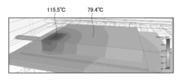
- Chip temperature distribution A schematic bird's-eye view of the chip temperature distribution simulation result of the semiconductor chip to which the thermal resistance analysis model according to the first embodiment is applied is expressed as shown in FIG. As shown in FIG. 15, the maximum temperature in the local heat generating portion is about 115.5 ° C., and the temperature of the central portion of the semiconductor chip is about 79.4 ° C.
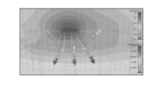
- FIG. 16 A schematic diagram of a heat flux simulation result in the vicinity of the junction node JN corresponding to the local heat generating portion of the semiconductor chip to which the thermal resistance analysis model according to the first embodiment is applied is expressed as shown in FIG.
- FIG. 16 when the heat flux is displayed as a vector, it can be seen that most of the heat flux flows downward (bottom inner node side: substrate side such as Cu). The heat flow rate flowing downward is about 2.94 W from the CFD simulation result.
- FIG. 10 a schematic diagram in the cross-sectional direction of the semiconductor chip 10 (PN) for explaining the appearance of the isothermal line ET from the junction node JN is shown in FIG. It is expressed as shown in (a).
- the isotherm ET is indicated by a broken line as shown in FIG.
- the thermal resistance between the isothermal lines ET near the junction node JN and the junction node JN is represented by, for example, ⁇ 1, and sequentially, the thermal resistance between the isothermal lines ET is represented by, for example, ⁇ 2 ⁇ ⁇ 3.
- FIG. 14 a schematic upper surface of the semiconductor chip 10 (PN) for explaining a state in which an isotherm is drawn from the junction node JN.
- the figure is represented as shown in FIG.
- the isotherm ET is indicated by a broken line as shown in FIG.
- the isotherm ET is drawn from the junction node JN to the semiconductor chip 10 (PN) center CE, and the thermal resistance ⁇ JP to that point is calculated.
- the semiconductor chip 10 (PN) center CE substantially corresponds to the plate node PN.
- the isotherm ET is drawn from the junction node JN at an arbitrary position to the semiconductor chip 10 (PN) center CE, and the thermal resistance up to that point is drawn.
- PN semiconductor chip 10
- the thermal resistance from the center CE of the semiconductor chip 10 (PN) to the bottom inner node BI is represented by ⁇ PBI.
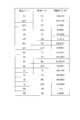
- the thermal resistance analysis result of each part of the semiconductor integrated circuit to which the local DELPHI model is applied as the thermal resistance analysis model according to the first embodiment is expressed as shown in FIG.
- the analysis result of the thermal resistance arranged between the start point node and the end point node is indicated by a numerical value (° C./W).
- the thermal resistance between the top inner node TI and the top outer node TO is 1480.252 (° C./W).
- the thermal resistance between the plate node PN and the junction node JN is 12.3 (° C./W).
- the thermal resistance between the plate node PN and the bottom inner node BI is 2.26567 (° C./W).
- thermal resistance ⁇ JA As a comparative example, a numerical example of the junction temperature and the thermal resistance ⁇ JA of the semiconductor chip at the time of local heat generation calculated by applying a detailed model is expressed as shown in FIG. In the detailed model, the maximum junction temperature is about 115.5 ° C., and the thermal resistance ⁇ JA is about 31.6 ° C./W.
- junction temperature and the thermal resistance ⁇ JA of the semiconductor chip during the entire heat generation calculated by applying the DELPHI model is expressed as shown in FIG.
- a junction temperature of about 91.9 ° C. and a thermal resistance ⁇ JA of about 23.7 ° C./W are obtained.
- thermal resistance analysis model numerical examples of the junction temperature and the thermal resistance ⁇ JA of the semiconductor chip to which the local DELPHI model is applied are expressed as shown in FIG.
- the maximum junction temperature is about 115.4 ° C.
- the thermal resistance ⁇ JA is about 31.6 ° C./W.
- the result calculated by applying the DELPHI model is a numerical example of the junction temperature and the thermal resistance ⁇ JA of the semiconductor chip when the entire surface generates heat. Therefore, a relative error compared to the result calculated by applying the detailed model. Is big.
- the result calculated by applying the local DELPHI model as the thermal resistance analysis model according to the first embodiment by adding the plate node PN, the junction temperature and thermal resistance ⁇ of the semiconductor chip at the time of local heat generation are obtained. Since this is a numerical example of JA, the error is relatively small compared with the result calculated by applying the detailed model, and a good result is obtained.
- FIG. 21A a schematic cross-sectional structure of a 1s (one layer) substrate is represented as shown in FIG. 21A, and a schematic cross-sectional structure of a 2s (two layer) substrate is shown in FIG.
- the schematic cross-sectional structure of the 2s2p (4-layer) substrate is expressed as shown in FIG.
- the 1s (single layer) substrate includes an insulating substrate 150 and a first electrode layer (footprint) S1 disposed on the insulating substrate 150, as shown in FIG.
- the semiconductor chip 10 is disposed on the first electrode layer (footprint) S1 via the die 14 (BI).
- the 2s (two-layer) substrate includes an insulating substrate 150, a first electrode layer (footprint) S1 disposed on the insulating substrate 150, and a first electrode layer of the insulating substrate 150.
- the second electrode layer S2 is provided on the back surface facing the S1.
- the 2s2p (four-layer) substrate includes an insulating substrate 150, a first electrode layer (footprint) S1 disposed on the insulating substrate 150, and a first electrode layer of the insulating substrate 150.
- (Footprint) Second electrode layer S2 disposed on the back surface facing S1, first plane electrode layer P1 embedded in insulating substrate 150, first plane electrode layer P1, and second electrode layer S2 And a second plane electrode layer P2 embedded in the inside of the insulating substrate 150.
- the semiconductor chip 10 is disposed on the first electrode layer (footprint) S1 via the die 14 (BI).
- the second electrode layer S2 can be applied as a ground electrode layer.
- the first plane electrode layer P1 may be held at the ground potential (GND), and the second plane electrode layer P2 may be held at the potential of the power supply voltage V CC .
- the heat source 1ch corresponds to, for example, a case where a heat source of a plurality of channels is assumed and only one channel among them generates heat.
- the multiple-channel heat source corresponds to, for example, a case in which a plurality of power transistors are arranged in parallel and a plurality of junction nodes are included.
- Tj is the junction temperature.
- TPN is the die temperature, which is the temperature of the die 14 called the bottom inner or island.
- Ta is the ambient temperature.
- P (W) is power consumption.
- ⁇ JA is a thermal resistance, and represents the thermal resistance between the junction node JN and the surrounding environment. In FIG. 20, the error of the thermal resistance ⁇ JA from the detailed model is also displayed in%.
- the local DELPHI model is applied as the thermal resistance analysis model according to the first embodiment, it can be sufficiently applied even when the heat dissipation performance of the substrate is changed.
- the description of the semiconductor integrated circuit 100 that considers heat dissipation toward the top surface of the semiconductor chip during local heat generation is expressed as shown in FIG. .
- the error can be reduced by adding a network to the upper surface side of the semiconductor chip.
- local heat generation can be modeled.
- thermo resistance analysis model as a thermal resistance analysis model of a semiconductor integrated circuit that locally generates heat, and a semiconductor integrated circuit to which this thermal resistance analysis model is applied.
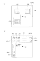
- a thermal resistance analysis model according to the second embodiment a bird's-eye view configuration of a semiconductor chip 10 to which a plurality of examples of local heat generation, that is, a local DELPHI model in which a plurality of junction nodes JN1 and JN2 and a plate node PN are added, 23 (a), and the description of the shape portion of the local DELPHI model is expressed as shown in FIG. 23 (b).
- a local DELPHI model expressing a plurality of local heat generations in the chip can be provided. It can. That is, in the thermal resistance analysis model according to the second embodiment, as shown in FIG. 23A, in the semiconductor chip 10, for example, the local heat generating portion in each junction portion such as two power transistors is a junction. The nodes JN1 and JN2 are expressed, and the semiconductor chip 10 portion other than the local heat generating portion is expressed by a plate node PN.
- the shape of the local DELPHI model expressing a plurality of local heat generations in the chip is as shown in FIG. It has a model that represents it.
- the local DELPHI model representing a plurality of local heat generations as a thermal resistance analysis model includes a junction node JN1, a junction node JN2, and a plate node as shown in FIG. PN, top inner node TI, top outer node TO, bottom inner node BI, bottom outer node BO, side node SI, lead node LE, junction node JN1, and top inner node TI
- Thermal resistance ⁇ J1TI thermal resistance ⁇ J1TO disposed between junction node JN1 and top outer node TO
- bottom inner node BI and the bottom outer node BO correspond to the inner portion and the outer portion of the mounting substrate portion on which the semiconductor chip 10 is mounted in the semiconductor integrated circuit, as in FIG.
- top inner node TI and the top outer node TO are, as in FIGS. 2 (a) and 3 (b), an inner portion and an outer portion of the upper surface case portion where the semiconductor chip 10 is disposed in the semiconductor integrated circuit. It corresponds to.
- junction nodes JN1 and JN2 correspond to junction portions that are a plurality of local heat sources of the semiconductor chip 10 in the semiconductor integrated circuit.
- the plate node PN is connected to the semiconductor chips 10 (other than the junction nodes JN1 and JN2 which are local heat sources of the semiconductor chip 10 in the semiconductor integrated circuit). PN).
- the side node SI and the lead node LE are provided in the side portion of the case portion on which the semiconductor chip 10 is mounted and the lead terminal arrangement portion in the semiconductor integrated circuit. It corresponds.
- a local DELPHI model that expresses a plurality of local heat generations in a chip expresses a local heat generation part with junction nodes JN1 and JN2, and the semiconductor chip 10 other than the local heat generation part 10
- the portion by the plate node PN a plurality of local heat generation in the semiconductor chip can be accurately expressed.
- FIG. 24 a schematic plan configuration of the integrated circuit 140 for system power supply is shown in FIG.
- FIG. 24 Schematic of DC / DC converter block 121 (JN1) and LDO regulator block 122 (JN2) having different heat generation profiles in system power supply integrated circuit 140 shown in FIG. 24A and corresponding to FIG.
- the target plane configuration is expressed as shown in FIG.
- FIG. 24 (a) the junction nodes JN1 and JN2 are shown, but the detailed description of other parts is omitted.
- the semiconductor chip 10 is disposed on the die 14 via the die connection part 12.
- the die 14 constitutes an island such as a metal layer mounted on the substrate, and corresponds to the bottom inner node BI in the local DELPHI model.
- the die connection part 12 is composed of a solder layer or the like that connects the die 14 and the semiconductor chip 10.
- the local heat generating portion of the semiconductor chip 10 is represented by junction nodes JN1 and JN2. Further, the semiconductor chip 10 portion other than the local heat generating portions (junction nodes JN1 and JN2) is represented by a plate node PN, but the center CE of the semiconductor chip 10 substantially corresponds to the plate node PN.
- the power transistor portions of the DC / DC converter block 121 (JN1) and the LDO regulator block 122 (JN2) are mainly used.
- a thermal resistance ⁇ JN1P is arranged between the junction node JN1 corresponding to the DC / DC converter block 121 and the center CE of the semiconductor chip 10, and the junction node JN2 corresponding to the LDO regulator block 122 and the semiconductor chip 10 are
- a thermal resistance ⁇ JN2P is arranged between the center CE.
- a thermal resistance ⁇ NPBI is disposed between the plate node PN and the bottom inner node BI.
- a local DELPHI model expressing a plurality of local heat generations is obtained by adding one plate node PN and adding a network to the junction nodes JN1 and N2.
- the local heat generation in the chip can be accurately expressed.
- a highly accurate thermal resistance analysis model as a thermal resistance analysis model of a semiconductor integrated circuit that locally generates heat at a plurality of locations, and a semiconductor integrated circuit to which this thermal resistance analysis model is applied are provided. Can do.
- FIG. 1 a schematic plan configuration of the semiconductor chip 10 to which the local DELPHI model is applied when there are three junction nodes JN1, JN2, and JN3 is shown in FIG. Represented as shown.
- FIG. 2 a schematic plan configuration of the semiconductor chip 10 to which the local DELPHI model is applied when there are a plurality of junction nodes JN1, JN2,..., JNm,.
- a schematic planar configuration is expressed as shown in FIG.
- the three junction nodes JN1, JN2, and JN3 may be expressed as a junction node JN.
- the three junction nodes JN1, JN2, and JN3 By expressing the three junction nodes JN1, JN2, and JN3 as a merged junction node JN, it can be handled in the same manner as the local DELPHI model having the junction node JN and the plate node PN.
- junction nodes JN1, JN2,..., JNm,..., JN2m, ..., JNn when there are a plurality of junction nodes JN1, JN2,..., JNm,..., JN2m, ..., JNn, as shown in FIG. JNm... JN2m... JNn may be expressed as a junction node JN.
- junction nodes JN1, JN2,..., JNm,..., JNn By representing a plurality of junction nodes JN1, JN2,..., JNm,..., JNn as junction nodes JN, they can be handled in the same manner as a local DELPHI model having junction nodes JN and plate nodes PN. it can.
- thermal resistance analysis model according to the third embodiment even when there is a multi-channel heat source, it can be handled in the same manner as the local DELPHI model having the junction node JN and the plate node PN.
- a highly accurate thermal resistance analysis model as a thermal resistance analysis model of a semiconductor integrated circuit that locally generates heat at a plurality of locations, and a semiconductor integrated circuit to which this thermal resistance analysis model is applied are provided. Can do.
- a highly accurate thermal resistance analysis model as a thermal resistance analysis model of a semiconductor integrated circuit that locally generates heat, and a semiconductor integrated circuit to which this thermal resistance analysis model is applied are provided. be able to.
- the present embodiment includes various embodiments that are not described here.
- the thermal resistance analysis model of the present embodiment can be applied to a semiconductor integrated circuit that generates locally heat, and it can be applied to a wide range of fields such as mobile devices, in-vehicle devices, industrial devices, medical devices, and display devices that use the semiconductor integrated circuits as electronic components. Applicable.
Landscapes
- Engineering & Computer Science (AREA)
- Physics & Mathematics (AREA)
- Theoretical Computer Science (AREA)
- Computer Hardware Design (AREA)
- General Physics & Mathematics (AREA)
- General Engineering & Computer Science (AREA)
- Geometry (AREA)
- Evolutionary Computation (AREA)
- Microelectronics & Electronic Packaging (AREA)
- Semiconductor Integrated Circuits (AREA)
- Lead Frames For Integrated Circuits (AREA)
- Architecture (AREA)
- Software Systems (AREA)
Abstract
熱抵抗解析モデルは、ボトムインナーノードBIを構成するダイ(14)と、ダイ(14)上に配置され、ジャンクションノードJNを構成する局所発熱部を有すると共に、追加のプレートノードPNを構成する半導体チップ(10)とを備える半導体集積回路(100)において、ジャンクションノードJNとプレートノードPN間の第1熱抵抗θJPと、プレートノードPNとボトムインナーノードBI間の第2熱抵抗θPBIを有し、半導体集積回路(100)を多熱抵抗ネットワークで表現した。局所発熱する半導体集積回路の熱抵抗解析モデルとして精度の良好な熱抵抗解析モデル、およびこの熱抵抗解析モデルを適用した半導体集積回路を提供する。
Description
本実施の形態は、熱抵抗解析モデル、および半導体集積回路に関する。
半導体集積回路の製造工程においては、構想設計、基本設計、詳細設計、試作/デバック、および設計変更/量産の手順を経過するが、対策の自由度は、初期工程が大きく、後工程に行くほど低下する。また、製造における対策コストは、初期工程が小さく、後工程に行くほど増大する。したがって、初期工程に重みを置くことでトータルの工数削減を図ることができる。半導体集積回路の熱設計においても、初期工程に重みを置くフロントローディング化を進める必要がある。
半導体集積回路部品の小型化に伴い、実装基板上における各発熱部品の配置によって、装置の周囲温度Taが大きく影響されるようになってきている。また、実装基板上における高密度実装に伴い、隣り合う半導体集積回路部品間で、熱的に干渉する状況も生じてきている。したがって、例えば、数値流体力学(CFD:Computational Fluid Dynamics)を適用した解析が必要になり、解析に必要な熱抵抗モデルの必要性は高まっている。
ジャンクション温度をはじめ、半導体集積回路各部の温度を高精度で予測するためには、内部構造の正確なモデルが必要となる。例えば、解析ツールとして、半導体集積回路の内部構造を考慮した高精度のモデルが提案されており、標準化団体の電子機器技術評議会(JEDEC:Joint Electron Device Engineering Councils)によって採用されている。
本実施の形態は、局所発熱する半導体集積回路の熱抵抗解析モデルとして精度の良好な熱抵抗解析モデル、およびこの熱抵抗解析モデルを適用した半導体集積回路を提供する。
本実施の形態の一態様によれば、ボトムインナーノードを構成するダイと、前記ダイ上に配置され、ジャンクションノードを構成する局所発熱部を有すると共に、追加のプレートノードを構成する半導体チップとを備える半導体集積回路において、前記ジャンクションノードと前記プレートノード間の第1熱抵抗と、前記プレートノードと前記ボトムインナーノード間の第2熱抵抗を有し、前記半導体集積回路を多熱抵抗ネットワークで表現した熱抵抗解析モデルが提供される。
本実施の形態の他の態様によれば、ボトムインナーノードを構成するダイと、前記ダイ上に配置され、第1ジャンクションノードを構成する第1局所発熱部と、前記第1局所発熱部と離隔され、第2ジャンクションノードを構成する第2局所発熱部とを有すると共に、追加のプレートノードを構成する半導体チップとを備える半導体集積回路において、前記第1ジャンクションノードと前記プレートノード間の第1熱抵抗と、前記プレートノードと前記ボトムインナーノード間の第2熱抵抗と、前記プレートノードと前記第2ジャンクションノード間の第3熱抵抗と、前記第1ジャンクションノードと前記第2ジャンクションノード間の第4熱抵抗とを有し、前記半導体集積回路を多熱抵抗ネットワークで表現した熱抵抗解析モデルが提供される。
本実施の形態の他の態様によれば、上記の熱抵抗解析モデルを適用した半導体集積回路が提供される。
本実施の形態によれば、局所発熱する半導体集積回路の熱抵抗解析モデルとして精度の良好な熱抵抗解析モデル、およびこの熱抵抗解析モデルを適用した半導体集積回路を提供することができる。
次に、図面を参照して、本実施の形態を説明する。以下の図面の記載において、同一又は類似の部分には同一又は類似の符号を付している。ただし、図面は模式的なものであり、厚みと平面寸法との関係、各層の厚みの比率等は現実のものとは異なることに留意すべきである。したがって、具体的な厚みや寸法は以下の説明を参酌して判断すべきものである。又、図面相互間においても互いの寸法の関係や比率が異なる部分が含まれていることはもちろんである。
又、以下に示す実施の形態は、技術的思想を具体化するための装置や方法を例示するものであって、構成部品の材質、形状、構造、配置等を下記のものに特定するものでない。この実施の形態は、特許請求の範囲において、種々の変更を加えることができる。
尚、以下の説明において、トップインナーノードTIを単にトップインナーTIと表現する場合もある。ボトムインナーノードBI、ボトムアウターノードBO、トップアウターノードTO、サイドノードSI、リードノードLE、リードフットノードLEFおよびリードサイドノードLESについても同様である。
[第1の実施の形態]
第1の実施の形態に係る熱抵抗解析モデルを適用する半導体集積回路100の鳥瞰構成例は、図1に示すように表される。半導体集積回路100内には、半導体(LSI)チップが搭載可能である。
第1の実施の形態に係る熱抵抗解析モデルを適用する半導体集積回路100の鳥瞰構成例は、図1に示すように表される。半導体集積回路100内には、半導体(LSI)チップが搭載可能である。
第1の実施の形態に係る熱抵抗解析モデルを適用する半導体集積回路100において、トップインナーTI、トップアウターTO、サイドSI、リードLEの各部の説明は、図2(a)に示すように表される。また、リードLEのリードフットLEFおよびリードサイドLESの各部の説明は、図2(b)に示すように表される。
第1の実施の形態に係る熱抵抗解析モデルを適用する半導体集積回路100において、ボトムインナーBI、ボトムアウターBOの各部の説明は、図3(a)に示すように表され、トップインナーTI、トップアウターTOの各部の説明は、図3(b)に示すように表される。また、ジャンクションノードJNの部分の説明は、図3(c)に示すように表される。また、サイドSI、リードLEの部分の説明は、図3(d)に示すように表される。
(比較例)
比較例に係るCFD適用熱抵抗解析モデルとしては、解析の目的に応じて、詳細モデル、DELPHIモデル、2抵抗モデルの3つのモデルから選択可能である。詳細モデルは、熱的に等価であることを利用して簡易化しながらも、出来る限り詳細に内部構造をモデル化する。2抵抗モデルは、一般的に最も簡易な形式で、形状を2つの熱抵抗として簡易的にモデル化する。DELPHIモデルは、6つ以上の熱抵抗でモデル化した、2抵抗モデルよりも詳細な熱抵抗モデルである。
比較例に係るCFD適用熱抵抗解析モデルとしては、解析の目的に応じて、詳細モデル、DELPHIモデル、2抵抗モデルの3つのモデルから選択可能である。詳細モデルは、熱的に等価であることを利用して簡易化しながらも、出来る限り詳細に内部構造をモデル化する。2抵抗モデルは、一般的に最も簡易な形式で、形状を2つの熱抵抗として簡易的にモデル化する。DELPHIモデルは、6つ以上の熱抵抗でモデル化した、2抵抗モデルよりも詳細な熱抵抗モデルである。
―2抵抗コンパクトモデル―
比較例に係るCFD適用熱抵抗解析モデルとして、2抵抗コンパクトモデル(JESD15-3)の形状の説明は、図4に示すように表される。2抵抗コンパクトモデル(JESD15-3)の形状は、図4に示すように、半導体集積回路100をジャンクションノードJNから上下に分けただけの簡単なモデルを備えている。すなわち、2抵抗コンパクトモデル(JESD15-3)は、図4に示すように、ジャンクションノードJNと、ケースノードCNと、ボードノードBNと、ジャンクションノードJN・ケースノードCN間に配置される熱抵抗θJCと、ジャンクションノードJN・ボードノードBN間に配置される熱抵抗θJBとを備える。ここで、ジャンクションノードJNは、半導体チップの熱源となるジャンクション部分に対応している。ケースノードCNは、ジャンクションノードJNから上方向に配置されるケース部分に対応している。また、ボードノードBNは、半導体チップが搭載される実装基板部分に対応している。
比較例に係るCFD適用熱抵抗解析モデルとして、2抵抗コンパクトモデル(JESD15-3)の形状の説明は、図4に示すように表される。2抵抗コンパクトモデル(JESD15-3)の形状は、図4に示すように、半導体集積回路100をジャンクションノードJNから上下に分けただけの簡単なモデルを備えている。すなわち、2抵抗コンパクトモデル(JESD15-3)は、図4に示すように、ジャンクションノードJNと、ケースノードCNと、ボードノードBNと、ジャンクションノードJN・ケースノードCN間に配置される熱抵抗θJCと、ジャンクションノードJN・ボードノードBN間に配置される熱抵抗θJBとを備える。ここで、ジャンクションノードJNは、半導体チップの熱源となるジャンクション部分に対応している。ケースノードCNは、ジャンクションノードJNから上方向に配置されるケース部分に対応している。また、ボードノードBNは、半導体チップが搭載される実装基板部分に対応している。
比較例に係るCFD適用熱抵抗解析モデルとして、2抵抗コンパクトモデル(JESD15-3)は、ジャンクションノードJNが1つのノードで構成されている。また、その発熱モデルとしての精度は低い。
―DELPHIコンパクトモデル―
比較例に係るCFD適用熱抵抗解析モデルとして、DELPHIコンパクトモデル(JESD15-4)の形状の説明は、図5に示すように表される。
比較例に係るCFD適用熱抵抗解析モデルとして、DELPHIコンパクトモデル(JESD15-4)の形状の説明は、図5に示すように表される。
DELPHIコンパクトモデル(JESD15-4)の形状は、図5に示すように、半導体集積回路を多熱抵抗ネットワークで表現したモデルを備えている。すなわち、DELPHIコンパクトモデル(JESD15-4)は、図5に示すように、ジャンクションノードJNと、トップインナーノードTIと、トップアウターノードTOと、ボトムインナーノードBIと、ボトムアウターノードBOと、サイドノードSIと、リードノードLEと、ジャンクションノードJN・トップインナーノードTI間に配置される熱抵抗θJTIと、ジャンクションノードJN・トップアウターノードTO間に配置される熱抵抗θJTOと、ジャンクションノードJN・サイドノードSI間に配置される熱抵抗θJSと、ジャンクションノードJN・リードノードLE間に配置される熱抵抗θJLと、ジャンクションノードJN・ボトムインナーノードBI間に配置される熱抵抗θJBIと、ジャンクションノードJN・ボトムアウターノードBO間に配置される熱抵抗θJBOと、トップインナーノードTI・トップアウターノードTO間に配置される熱抵抗θTIOと、トップインナーノードTI・サイドノードSI間に配置される熱抵抗θTSと、トップアウターノードTO・リードノードLE間に配置される熱抵抗θTLと、サイドノードSI・ボトムインナーノードBI間に配置される熱抵抗θS Bと、リードノードLE・ボトムアウターノードBO間に配置される熱抵抗θLBと、ボトムインナーノードBI・ボトムアウターノードBO間に配置される熱抵抗θBIOとを備える。
また、ボトムインナーノードBIとボトムアウターノードBOは、図3(a)に示すように、半導体集積回路内において、半導体チップが搭載される実装基板部分の内側部分および外側部分に対応している。
また、トップインナーノードTIとトップアウターノードTOは、図2(a)・図3(b)に示すように、半導体集積回路内において、半導体チップが配置される上面ケース部分の内側部分および外側部分に対応している。
また、ジャンクションノードJNは、図3(c)に示すように、半導体集積回路内において、半導体チップの熱源となるジャンクション部分に対応している。
また、サイドノードSIとリードノードLEは、図2(a)・図3(d)に示すように、半導体集積回路内において、半導体チップを搭載するケース部分のサイド部分およびリード端子の配置部分に対応している。
比較例に係る熱抵抗解析モデルとして、DELPHIコンパクトモデル(JESD15-4)は、ジャンクションノードJNが1つのノードで構成されている。また、その発熱モデルとしての精度は良好であるが、局所発熱に対しては、対応することが困難である。
―詳細モデル―
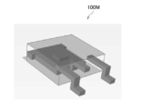
比較例に係るCFD適用熱抵抗解析モデルとして、半導体集積回路100Mの詳細モデル(規格無)の形状の説明は、図6に示すように表される。すなわち、詳細モデルは、半導体集積回路100Mを構成する半導体チップや各構成部分の寸法、物性値などが含まれているため、抽象度の低いモデルである。詳細モデルは、その発熱モデルとしての精度は精度は最良であるが、内部の詳細な情報が含まれるため、実際上は入手困難であり、また、規格が無く、品質は各社各様である。また、詳細なモデルであるため、計算時間がかかり、解析ツール間の互換性が低い。
比較例に係るCFD適用熱抵抗解析モデルとして、半導体集積回路100Mの詳細モデル(規格無)の形状の説明は、図6に示すように表される。すなわち、詳細モデルは、半導体集積回路100Mを構成する半導体チップや各構成部分の寸法、物性値などが含まれているため、抽象度の低いモデルである。詳細モデルは、その発熱モデルとしての精度は精度は最良であるが、内部の詳細な情報が含まれるため、実際上は入手困難であり、また、規格が無く、品質は各社各様である。また、詳細なモデルであるため、計算時間がかかり、解析ツール間の互換性が低い。
比較例に係る詳細モデルは入手性に難が有る。また、比較例に係る2抵抗モデルは、詳細設計には、使えない。一方、比較例に係るDELPHIモデルが現実的であるが、局所発熱に対しては、対応することが困難である。
(全面発熱時)
比較例として、詳細モデルを適用して計算した全面発熱時の半導体チップのジャンクション温度と熱抵抗θJAの数値例は、図7に示すように表される。図7に示す例では、ジャンクション温度=82.5℃、熱抵抗θJA=20.6℃/Wである。
比較例として、詳細モデルを適用して計算した全面発熱時の半導体チップのジャンクション温度と熱抵抗θJAの数値例は、図7に示すように表される。図7に示す例では、ジャンクション温度=82.5℃、熱抵抗θJA=20.6℃/Wである。
比較例として、DELPHIモデルを適用して計算した全面発熱時の半導体チップのジャンクション温度と熱抵抗θJAの数値例は、図8に示すように表される。図8に示す例では、ジャンクション温度=82.6℃、熱抵抗θJA=20.7℃/Wである。
比較例として、DELPHIモデルを適用して計算した全面発熱時の半導体チップのジャンクション温度と熱抵抗θJAの計算結果では、詳細モデルの計算結果と略一致しており、全面発熱時の発熱モデルとしての精度は良好である。
(局所発熱時)
比較例として、詳細モデルを適用して計算した局所発熱時の半導体チップのジャンクション温度と熱抵抗θJAの数値例は、図9に示すように表される。図9においては、熱源が複数のチャネルを有する半導体チップにおいて、その内の1チャネルのみが発熱する局所発熱時を想定している。図9に示す例では、接合最高温度=115.5℃、熱抵抗θJA=31.6℃/Wである。
比較例として、詳細モデルを適用して計算した局所発熱時の半導体チップのジャンクション温度と熱抵抗θJAの数値例は、図9に示すように表される。図9においては、熱源が複数のチャネルを有する半導体チップにおいて、その内の1チャネルのみが発熱する局所発熱時を想定している。図9に示す例では、接合最高温度=115.5℃、熱抵抗θJA=31.6℃/Wである。
比較例として、DELPHIモデルを適用して計算した局所発熱時の半導体チップのジャンクション温度と熱抵抗θJAの数値例は、図10に示すように表される。図10に示す例では、ジャンクション温度=91.9℃、熱抵抗θJA=23.7℃/Wである。
比較例として、DELPHIモデルを適用して計算した局所発熱時の半導体チップのジャンクション温度と熱抵抗θJAの計算結果では、詳細モデルの計算結果とは、大きく異なった値を示しており、局所発熱時の発熱モデルとしての精度は低い。DELPHIモデルは、局所発熱には対応していない。
(比較例:DELPHIモデル)
比較例として、DELPHIモデルを適用する全面発熱時の半導体チップ10の鳥瞰構成は、図11(a)に示すように表され、図11(a)に対応するDELPHIモデル形状の説明は、図11(b)に示すように表される。DELPHIモデルを適用する全面発熱時の半導体チップ10では、図11(a)に示すように、半導体チップ10全体が、ジャンクションノードJNそのものとして表される。図11(a)に対応するDELPHIモデル形状を説明する図11(b)の構成は、図5に示したDELPHIコンパクトモデル(JESD15-4)の形状と同様に、半導体集積回路を多熱抵抗ネットワークで表現したモデルを備えているため、重複説明は省略する。
比較例として、DELPHIモデルを適用する全面発熱時の半導体チップ10の鳥瞰構成は、図11(a)に示すように表され、図11(a)に対応するDELPHIモデル形状の説明は、図11(b)に示すように表される。DELPHIモデルを適用する全面発熱時の半導体チップ10では、図11(a)に示すように、半導体チップ10全体が、ジャンクションノードJNそのものとして表される。図11(a)に対応するDELPHIモデル形状を説明する図11(b)の構成は、図5に示したDELPHIコンパクトモデル(JESD15-4)の形状と同様に、半導体集積回路を多熱抵抗ネットワークで表現したモデルを備えているため、重複説明は省略する。
(第1の実施の形態:局所DELPHIモデル)
第1の実施の形態に係る熱抵抗解析モデルとして、局所DELPHIモデルを適用する半導体チップ10の鳥瞰構成は、図12(a)に示すように表され、図12(a)に対応する局所DELPHIモデルの形状の説明は、図12(b)に示すように表される。
第1の実施の形態に係る熱抵抗解析モデルとして、局所DELPHIモデルを適用する半導体チップ10の鳥瞰構成は、図12(a)に示すように表され、図12(a)に対応する局所DELPHIモデルの形状の説明は、図12(b)に示すように表される。
第1の実施の形態に係る熱抵抗解析モデルにおいては、1つプレートノードPNを追加することで、半導体チップ10内の局所発熱を表現する局所DELPHIモデルを提供することができる。すなわち、第1の実施の形態に係る熱抵抗解析モデルにおいては、図12(a)に示すように、半導体チップ10において、例えばパワートランジスタなどのジャンクション部における局所発熱部をジャンクションノードJNで表現し、局所発熱部以外の半導体チップ10部分をプレートノードPNで表現する。
第1の実施の形態に係る熱抵抗解析モデルとして、局所DELPHIモデルの形状は、図12(b)に示すように、半導体集積回路を多熱抵抗ネットワークで表現したモデルを備えている。
すなわち、第1の実施の形態に係る熱抵抗解析モデルとしての局所DELPHIモデルは、図12(b)に示すように、ジャンクションノードJNと、追加されたプレートノードPNと、トップインナーノードTIと、トップアウターノードTOと、ボトムインナーノードBIと、ボトムアウターノードBOと、サイドノードSIと、リードノードLEと、ジャンクションノードJN・トップインナーノードTI間に配置される熱抵抗θJTIと、ジャンクションノードJN・トップアウターノードTO間に配置される熱抵抗θJTOと、ジャンクションノードJN・サイドノードSI間に配置される熱抵抗θJSと、ジャンクションノードJN・リードノードLE間に配置される熱抵抗θJLと、ジャンクションノードJN・プレートノードPN間に配置される熱抵抗θJPと、プレートノードPN・ボトムインナーノードBI間に配置される熱抵抗θPBIと、ジャンクションノードJN・ボトムアウターノードBO間に配置される熱抵抗θJBOと、トップインナーノードTI・トップアウターノードTO間に配置される熱抵抗θTIOと、トップインナーノードTI・サイドノードSI間に配置される熱抵抗θTSと、トップアウターノードTO・リードノードLE間に配置される熱抵抗θTLと、サイドノードSI・ボトムインナーノードBI間に配置される熱抵抗θSBと、リードノードLE・ボトムアウターノードBO間に配置される熱抵抗θLBと、ボトムインナーノードBI・ボトムアウターノードBO間に配置される熱抵抗θBIOとを備える。
また、ボトムインナーノードBIとボトムアウターノードBOは、図3(a)と同様に、半導体集積回路内において、半導体チップ10が搭載される実装基板部分の内側部分および外側部分に対応している。
また、トップインナーノードTIとトップアウターノードTOは、図2(a)・図3(b)と同様に、半導体集積回路内において、半導体チップ10が配置される上面ケース部分の内側部分および外側部分に対応している。
また、ジャンクションノードJNは、図12(a)に示すように、半導体集積回路内において、半導体チップ10の局所的な熱源となるジャンクション部分に対応している。
また、追加のプレートノードPNは、図12(a)に示すように、半導体集積回路内において、半導体チップ10の局所的な熱源となるジャンクションノードJN以外の半導体チップ10(PN)に対応している。
また、サイドノードSIとリードノードLEは、図2(a)・図3(d)と同様に、半導体集積回路内において、半導体チップ10を搭載するケース部分のサイド部分およびリード端子の配置部分に対応している。
第1の実施の形態に係る熱抵抗解析モデルとしての局所DELPHIモデルは、1つプレートノードPNを追加して、局所発熱部をジャンクションノードJNで表現し、局所発熱部以外の半導体チップ10部分をプレートノードPNで表現することによって、チップ内の局所発熱を精度よく表現することができる。
第1の実施の形態に係る熱抵抗解析モデルとして、プレートノードPNを追加した局所DELPHIモデルにおいて、ジャンクションノードJN・ボトムインナーノードBI間の形状の説明は、図13に示すように表される。図13は、図12(b)の破線部分を抽出したものである。
第1の実施の形態に係る熱抵抗解析モデルとして、プレートノードPNを追加した局所DELPHIモデルを適用する半導体集積回路100の鳥瞰構成は、図14に示すように表される。
第1の実施の形態に係る熱抵抗解析モデルとして、局所DELPHIモデルを適用する半導体集積回路100は、図14に示すように、ダイ14と、ダイ接続部12と、半導体チップ10とを備える。
半導体チップ10は、ダイ14上にダイ接続部12を介して配置される。
ダイ14は、基板上に搭載される金属層などのアイランドを構成し、局所DELPHIモデルにおけるボトムインナーノードBIに対応している。
ダイ接続部12は、ダイ14と半導体チップ10を接続する半田層等で構成される。
半導体チップ10の局所発熱部は、ジャンクションノードJNで表されている。また、局所発熱部(ジャンクションノードJN)以外の半導体チップ10部分は、プレートノードPNで表されているが、実質的に半導体チップ10の中心CEがプレートノードPNに対応している。すなわち、半導体チップ10は、例えばパワートランジスタなどのジャンクション部からなる局所発熱部(ジャンクションノードJN)と、局所発熱部(JN)以外の半導体チップ10(プレートノードPN)とを備える。
ジャンクションノードJN・プレートノードPN(CE)間には、熱抵抗θJPが配置され、プレートノードPN・ボトムインナーノードBI間には、熱抵抗θPBIが配置されている。
第1の実施の形態に係る熱抵抗解析モデルとしての局所DELPHIモデルは、1つプレートノードPNを追加し、ネットワークを追加することによって、チップ内の局所発熱を精度よく表現することができる。
(チップ温度分布)
第1の実施の形態に係る熱抵抗解析モデルを適用した半導体チップのチップ温度分布シミュレーション結果の模式的鳥瞰図は、図15に示すように表される。図15に示すように、局所発熱部における最高温度は約115.5℃であり、半導体チップの中心部分の温度は、約79.4℃である。
第1の実施の形態に係る熱抵抗解析モデルを適用した半導体チップのチップ温度分布シミュレーション結果の模式的鳥瞰図は、図15に示すように表される。図15に示すように、局所発熱部における最高温度は約115.5℃であり、半導体チップの中心部分の温度は、約79.4℃である。
(ジャンクション部の熱流束)
第1の実施の形態に係る熱抵抗解析モデルを適用した半導体チップの局所発熱部に対応するジャンクションノードJN近傍の熱流束シミュレーション結果の模式図は、図16に示すように表される。図16に示すように、熱流束をベクトル表示すると、ほとんどが下側(ボトムインナーノード側:Cuなどの基板側)に流れていることがわかる。下側に流れる熱流量は、CFDのシミュレーション結果より約2.94Wである。以上より追加する熱抵抗θJPを計算すると、θJP=(115.5℃-79.4℃)/2.94W=12.3℃/Wで表される。
第1の実施の形態に係る熱抵抗解析モデルを適用した半導体チップの局所発熱部に対応するジャンクションノードJN近傍の熱流束シミュレーション結果の模式図は、図16に示すように表される。図16に示すように、熱流束をベクトル表示すると、ほとんどが下側(ボトムインナーノード側:Cuなどの基板側)に流れていることがわかる。下側に流れる熱流量は、CFDのシミュレーション結果より約2.94Wである。以上より追加する熱抵抗θJPを計算すると、θJP=(115.5℃-79.4℃)/2.94W=12.3℃/Wで表される。
(ジャンクションノードJNから等温線を引いた様子)
第1の実施の形態に係る熱抵抗解析モデルを適用した半導体集積回路において、ジャンクションノードJNから等温線ETを引いた様子を説明する半導体チップ10(PN)の断面方向の模式図は、図17(a)に示すように表される。等温線ETは、図17(a)に示すように、破線で示されている。ジャンクションノードJNとジャンクションノードJN近い等温線ET間の熱抵抗は、例えばθ1で表され、また順次、等温線ET間の熱抵抗は、例えばθ2・θ3で表されている。
第1の実施の形態に係る熱抵抗解析モデルを適用した半導体集積回路において、ジャンクションノードJNから等温線ETを引いた様子を説明する半導体チップ10(PN)の断面方向の模式図は、図17(a)に示すように表される。等温線ETは、図17(a)に示すように、破線で示されている。ジャンクションノードJNとジャンクションノードJN近い等温線ET間の熱抵抗は、例えばθ1で表され、また順次、等温線ET間の熱抵抗は、例えばθ2・θ3で表されている。
また、第1の実施の形態に係る熱抵抗解析モデルを適用した図14に対応する半導体集積回路において、ジャンクションノードJNから等温線を引いた様子を説明する半導体チップ10(PN)の模式的上面図は、図17(b)に示すように表される。同様に、等温線ETは、図17(b)に示すように、破線で示されている。
図17に示すように、ジャンクションノードJNから半導体チップ10(PN)中心CEまで等温線ETを引いて、そこまでの熱抵抗θJPを算出する。半導体チップ10(PN)中心CEが、実質的にプレートノードPNに対応している。
第1の実施の形態に係る熱抵抗解析モデルを適用した局所DELPHIモデルにおいては、任意の位置のジャンクションノードJNから半導体チップ10(PN)中心CEまで等温線ETを引いて、そこまでの熱抵抗θJPを算出することによって、半導体チップ10(PN)の上面の面最適化を図ることができる。さらに、半導体チップ10(PN)の中心CEからボトムインナーノードBIまでの熱抵抗が、θPBIで表される。
(各部の熱抵抗解析の具体例)
第1の実施の形態に係る熱抵抗解析モデルとして局所DELPHIモデルを適用した半導体集積回路の各部の熱抵抗解析結果は、図18に示すように表される。図18に示すように、始点ノード・終点ノード間に配置される熱抵抗の解析結果が数値(℃/W)で示されている。例えば、トップインナーノードTI・トップアウターノードTO間の熱抵抗は、1480.252(℃/W)である。プレートノードPN・ジャンクションノードJN間の熱抵抗は、12.3(℃/W)である。プレートノードPN・ボトムインナーノードBI間の熱抵抗は、2.26567(℃/W)である。
第1の実施の形態に係る熱抵抗解析モデルとして局所DELPHIモデルを適用した半導体集積回路の各部の熱抵抗解析結果は、図18に示すように表される。図18に示すように、始点ノード・終点ノード間に配置される熱抵抗の解析結果が数値(℃/W)で示されている。例えば、トップインナーノードTI・トップアウターノードTO間の熱抵抗は、1480.252(℃/W)である。プレートノードPN・ジャンクションノードJN間の熱抵抗は、12.3(℃/W)である。プレートノードPN・ボトムインナーノードBI間の熱抵抗は、2.26567(℃/W)である。
(熱抵抗θJAの数値例)
比較例として、詳細モデルを適用して計算した局所発熱時の半導体チップのジャンクション温度と熱抵抗θJAの数値例は、図19(a)に示すように表される。詳細モデルにおいては、最高ジャンクション温度は、約115.5℃、熱抵抗θJAは、約31.6℃/Wが得られている。
比較例として、詳細モデルを適用して計算した局所発熱時の半導体チップのジャンクション温度と熱抵抗θJAの数値例は、図19(a)に示すように表される。詳細モデルにおいては、最高ジャンクション温度は、約115.5℃、熱抵抗θJAは、約31.6℃/Wが得られている。
比較例として、DELPHIモデルを適用して計算した全面発熱時の半導体チップのジャンクション温度と熱抵抗θJAの数値例は、図19(b)に示すように表される。
DELPHIモデルにおいては、ジャンクション温度は、約91.9℃、熱抵抗θJAは、約23.7℃/Wが得られている。
DELPHIモデルにおいては、ジャンクション温度は、約91.9℃、熱抵抗θJAは、約23.7℃/Wが得られている。
一方、第1の実施の形態に係る熱抵抗解析モデルとして、局所DELPHIモデルを適用する半導体チップのジャンクション温度と熱抵抗θJAの数値例は、図19(c)に示すように表される。局所DELPHIモデルにおいては、最高ジャンクション温度は、約115.4℃、熱抵抗θJAは、約31.6℃/Wが得られている。
DELPHIモデルを適用して計算した結果では、全面発熱時の半導体チップのジャンクション温度と熱抵抗θJAの数値例となるため、詳細モデルを適用して計算した結果と比較して、相対的に誤差が大きい。
一方、第1の実施の形態に係る熱抵抗解析モデルとして、局所DELPHIモデルを適用して計算した結果では、プレートノードPNを追加することによって、局所発熱時の半導体チップのジャンクション温度と熱抵抗θJAの数値例となるため、詳細モデルを適用して計算した結果と比較して、相対的に誤差小さく、良好な結果がえられている。
(基板の放熱性能)
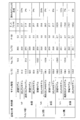
様々な基板仕様および、発熱源を全面および局所とする場合において、比較例として、詳細モデルおよびDELPHIモデルを適用して計算した数値例、第1の実施の形態に係る熱抵抗解析モデルとして、局所DELPHIモデルを適用して計算した数値例は、図20に示すように表される。
様々な基板仕様および、発熱源を全面および局所とする場合において、比較例として、詳細モデルおよびDELPHIモデルを適用して計算した数値例、第1の実施の形態に係る熱抵抗解析モデルとして、局所DELPHIモデルを適用して計算した数値例は、図20に示すように表される。
基板仕様について、図21(a)・図21(b)・図21(c)を参照して説明する。
図20における基板仕様として、1s(1層)基板の模式的断面構造は図21(a)に示すように表され、2s(2層)基板の模式的断面構造は図21(b)に示すように表され、2s2p(4層)基板の模式的断面構造は図21(c)に示すように表される。
1s(1層)基板は、図21(a)に示すように、絶縁基板150と、絶縁基板150上に配置された第1電極層(フットプリント)S1とを備える。第1電極層(フットプリント)S1上にはダイ14(BI)を介して半導体チップ10が配置される。
2s(2層)基板は、図21(b)に示すように、絶縁基板150と、絶縁基板150上に配置された第1電極層(フットプリント)S1と、絶縁基板150の第1電極層(フットプリント)S1に対向する裏面上に配置された第2電極層S2とを備える。
2s2p(4層)基板は、図21(c)に示すように、絶縁基板150と、絶縁基板150上に配置された第1電極層(フットプリント)S1と、絶縁基板150の第1電極層(フットプリント)S1に対向する裏面上に配置された第2電極層S2と、絶縁基板150の内部に埋め込まれた第1プレーン電極層P1と、第1プレーン電極層P1と第2電極層S2との間の絶縁基板150の内部に埋め込まれた第2プレーン電極層P2とを備える。第1電極層(フットプリント)S1上にはダイ14(BI)を介して半導体チップ10が配置される。第2電極層S2は、接地電極層として適用可能である。第1プレーン電極層P1は、接地電位(GND)に保持され、第2プレーン電極層P2は、電源電圧VCCの電位に保持されていても良い。
発熱源1chとは、例えば、複数チャネルの発熱源を想定して、その中の1チャネルのみが発熱した場合に対応している。複数チャネルの発熱源とは、例えば、パワートランジスタが複数個並列に配置された構成において、複数のジャンクションノードを有する場合などに対応する。
Tjはジャンクション温度である。TPNはダイ温度であり、ボトムインナー或いはアイランドと呼ばれるダイ14の温度である。Taは周囲温度である。P(W)は消費電力である。また、θJAは熱抵抗であり、ジャンクションノードJNと周囲環境間の熱抵抗を表す。図20においては、詳細モデルとの熱抵抗θJAの誤差についても%表示されている。
全面発熱源の場合には、図20に示すように、基板の放熱性能をパラメータにして、詳細モデルとDELPHIモデルの差を確認すると、2s2p(4層)構造および2s(2層)構造では、誤差が無いが、1s(1層)構造では、基板の放熱性能が相対的に低いため、約3%の誤差を生じている。
局所発熱源(1ch)の場合には、図20に示すように、基板の放熱性能をパラメータにして、詳細モデルとDELPHIモデルの差を確認すると、2s2p(4層)構造では、約33%の誤差を示し、2s(2層)構造では、約29%の誤差を示し、1s(1層)構造では、約12%の誤差を示している。一方、詳細モデルと局所DELPHIモデルの差を確認すると、2s2p(4層)構造では、誤差が無く、2s(2層)構造では、約3%の誤差を示し、1s(1層)構造では、約7%の誤差を示している。
局所DELPHIモデルは、基板の放熱性能が相対的に低くなるにつれて、相対的に誤差が増加する傾向が観られるが、詳細モデルとの誤差の範囲は、約10%以下である。
したがって、第1の実施の形態に係る熱抵抗解析モデルとして、局所DELPHIモデルを適用すれば、基板の放熱性能が変わった場合に対しても十分に適用可能である。
また、半導体チップ上面への放熱が増える(下面の基板側への放熱能力低下)ことによって、誤差は大きくなる傾向が観られるが、半導体チップ上面側へのネットワークを追加することで、影響緩和ができる。
第1の実施の形態に係る熱抵抗解析モデルとしての局所DELPHIモデルにおいて、局所発熱時の半導体チップ上面方向への放熱を考慮する半導体集積回路100の説明は、図22に示すように表される。図22に示すように、半導体チップ10の局所発熱源としてのジャンクションノードJNから樹脂モールド層200を介した上面方向への熱流TFuと、半導体チップ10・ダイ14を介した絶縁基板150方向への熱流TFdとの両方を考慮する。すなわち、半導体チップ上面側へのネットワークを追加することによって、誤差を縮小することができる。
第1の実施の形態に係る熱抵抗解析モデルとして、ノードを追加した局所DELPHIモデルによれば、局所発熱をモデル化可能である。
第1の実施の形態によれば、局所発熱する半導体集積回路の熱抵抗解析モデルとして精度の良好な熱抵抗解析モデル、およびこの熱抵抗解析モデルを適用した半導体集積回路を提供することができる。
[第2の実施の形態:複数の局所発熱例]
第2の実施の形態に係る熱抵抗解析モデルとして、複数の局所発熱例、すなわち複数のジャンクションノードJN1・JN2およびプレートノードPNを追加した局所DELPHIモデルを適用する半導体チップ10の鳥瞰構成は、図23(a)に示すように表され、その局所DELPHIモデルの形状部分の説明は、図23(b)に示すように表される。
第2の実施の形態に係る熱抵抗解析モデルとして、複数の局所発熱例、すなわち複数のジャンクションノードJN1・JN2およびプレートノードPNを追加した局所DELPHIモデルを適用する半導体チップ10の鳥瞰構成は、図23(a)に示すように表され、その局所DELPHIモデルの形状部分の説明は、図23(b)に示すように表される。
第2の実施の形態に係る熱抵抗解析モデルにおいては、2つジャンクションノードJN1・JN2とプレートノードPNを追加することで、チップ内の複数の局所発熱を表現する局所DELPHIモデルを提供することもできる。すなわち、第2の実施の形態に係る熱抵抗解析モデルにおいては、図23(a)に示すように、半導体チップ10において、例えば2個のパワートランジスタなどのそれぞれのジャンクション部における局所発熱部をジャンクションノードJN1、JN2で表現し、局所発熱部以外の半導体チップ10部分をプレートノードPNで表現する。
第2の実施の形態に係る熱抵抗解析モデルとして、チップ内の複数の局所発熱を表現する局所DELPHIモデルの形状は、図23(b)に示すように、半導体集積回路を多熱抵抗ネットワークで表現したモデルを備えている。
すなわち、第2の実施の形態に係る熱抵抗解析モデルとしての複数の局所発熱を表現する局所DELPHIモデルは、図23(b)に示すように、ジャンクションノードJN1と、ジャンクションノードJN2と、プレートノードPNと、トップインナーノードTIと、トップアウターノードTOと、ボトムインナーノードBIと、ボトムアウターノードBOと、サイドノードSIと、リードノードLEと、ジャンクションノードJN1・トップインナーノードTI間に配置される熱抵抗θJ1TIと、ジャンクションノードJN1・トップアウターノードTO間に配置される熱抵抗θJ1TOと、ジャンクションノードJN1・サイドノードSI間に配置される熱抵抗θJ1Sと、ジャンクションノードJN1・ジャンクションノードJN2間に配置される熱抵抗θJ12と、ジャンクションノードJN2・トップインナーノードTI間に配置される熱抵抗θJ2TIと、ジャンクションノードJN2・トップアウターノードTO間に配置される熱抵抗θJ2TOと、ジャンクションノードJN2・リードノードLE間に配置される熱抵抗θJ2Lと、ジャンクションノードJN2・ボトムアウターノードBO間に配置される熱抵抗θJ2Bと、ジャンクションノードJN2・プレートノードPN間に配置される熱抵抗θJN2Pと、ジャンクションノードJN1・プレートノードPN間に配置される熱抵抗θJN1Pと、プレートノードPN・ボトムインナーノードBI間に配置される熱抵抗θNPBIと、ジャンクションノードJN1・ボトムアウターノードBO間に配置される熱抵抗θJ1BOと、トップインナーノードTI・トップアウターノードTO間に配置される熱抵抗θTIOと、トップインナーノードTI・サイドノードSI間に配置される熱抵抗θTSと、トップアウターノードTO・リードノードLE間に配置される熱抵抗θTLと、サイドノードSI・ボトムインナーノードBI間に配置される熱抵抗θSBと、リードノードLE・ボトムアウターノードBO間に配置される熱抵抗θLBと、ボトムインナーノードBI・ボトムアウターノードBO間に配置される熱抵抗θBIOとを備える。
また、ボトムインナーノードBIとボトムアウターノードBOは、図3(a)と同様に、半導体集積回路内において、半導体チップ10が搭載される実装基板部分の内側部分および外側部分に対応している。
また、トップインナーノードTIとトップアウターノードTOは、図2(a)・図3(b)と同様に、半導体集積回路内において、半導体チップ10が配置される上面ケース部分の内側部分および外側部分に対応している。
また、ジャンクションノードJN1・JN2は、図23(a)に示すように、半導体集積回路内において、半導体チップ10の複数の局所的な熱源となるジャンクション部分に対応している。
また、プレートノードPNは、図23(a)・図23(b)に示すように、半導体集積回路内において、半導体チップ10の局所的な熱源となるジャンクションノードJN1・JN2以外の半導体チップ10(PN)に対応している。
また、サイドノードSIとリードノードLEは、図2(a)・図3(d)と同様に、半導体集積回路内において、半導体チップ10を搭載するケース部分のサイド部分およびリード端子の配置部分に対応している。
第2の実施の形態に係る熱抵抗解析モデルとして、チップ内の複数の局所発熱を表現する局所DELPHIモデルは、局所発熱部をジャンクションノードJN1・JN2で表現し、局所発熱部以外の半導体チップ10部分をプレートノードPNで表現することによって、半導体チップ内の複数の局所発熱を精度よく表現することができる。
(具体例)
第2の実施の形態に係る熱抵抗解析モデルとして、半導体チップ内の複数の局所発熱を表現する局所DELPHIモデルを適用する具体例として、システム電源用集積回路140の模式的平面構成は、図24(a)に示すように表され、図24(a)に対応するシステム電源用集積回路140において、それぞれ発熱プロファイルが異なるDC/DCコンバータブロック121(JN1)およびLDOレギュレータブロック122(JN2)の模式的平面構成は、図24(b)に示すように表される。また、第2の実施の形態に係る熱抵抗解析モデルとして、複数の局所発熱を表現する局所DELPHIモデルを適用する半導体集積回路100の鳥瞰構成は、図24(c)に示すように表される。なお、図24(a)においてはジャンクションノードJN1・JN2については表示しているが、その他の各部の詳細説明は省略する。
第2の実施の形態に係る熱抵抗解析モデルとして、半導体チップ内の複数の局所発熱を表現する局所DELPHIモデルを適用する具体例として、システム電源用集積回路140の模式的平面構成は、図24(a)に示すように表され、図24(a)に対応するシステム電源用集積回路140において、それぞれ発熱プロファイルが異なるDC/DCコンバータブロック121(JN1)およびLDOレギュレータブロック122(JN2)の模式的平面構成は、図24(b)に示すように表される。また、第2の実施の形態に係る熱抵抗解析モデルとして、複数の局所発熱を表現する局所DELPHIモデルを適用する半導体集積回路100の鳥瞰構成は、図24(c)に示すように表される。なお、図24(a)においてはジャンクションノードJN1・JN2については表示しているが、その他の各部の詳細説明は省略する。
第2の実施の形態に係る熱抵抗解析モデルとして、複数の局所発熱を表現する局所DELPHIモデルを適用する半導体集積回路100は、図24(c)に示すように、ダイ14と、ダイ接続部12と、半導体チップ10とを備える。
半導体チップ10は、ダイ14上にダイ接続部12を介して配置される。
ダイ14は、基板上に搭載される金属層などのアイランドを構成し、局所DELPHIモデルにおけるボトムインナーノードBIに対応している。
ダイ接続部12は、ダイ14と半導体チップ10を接続する半田層等で構成される。
半導体チップ10の局所発熱部は、ジャンクションノードJN1・JN2で表されている。また、局所発熱部(ジャンクションノードJN1・JN2)以外の半導体チップ10部分は、プレートノードPNで表されているが、実質的に半導体チップ10の中心CEがプレートノードPNに対応している。
システム電源用集積回路140においては、図24(a)・図24(b)に示すように、主として、DC/DCコンバータブロック121(JN1)・LDOレギュレータブロック122(JN2)のそれぞれのパワートランジスタ部分において局所発熱を生じる。このため、DC/DCコンバータブロック121に対応するジャンクションノードJN1と半導体チップ10の中心CEとの間には、熱抵抗θJN1Pが配置され、LDOレギュレータブロック122に対応するジャンクションノードJN2と半導体チップ10の中心CEとの間には、熱抵抗θJN2Pが配置される。プレートノードPN・ボトムインナーノードBI間には、熱抵抗θNPBIが配置されている。
第2の実施の形態に係る熱抵抗解析モデルとして、複数の局所発熱を表現する局所DELPHIモデルは、ジャンクションノードJN1・N2に対して、1つプレートノードPNを追加し、ネットワークを追加することによって、チップ内の局所発熱を精度よく表現することができる。
第2の実施の形態によれば、複数箇所で局所発熱する半導体集積回路の熱抵抗解析モデルとして精度の良好な熱抵抗解析モデル、およびこの熱抵抗解析モデルを適用した半導体集積回路を提供することができる。
[第3の実施の形態:複数の局所発熱例]
第3の実施の形態に係る熱抵抗解析モデルとして、3個のジャンクションノードJN1・JN2・JN3を有する場合に局所DELPHIモデルを適用する半導体チップ10の模式的平面構成は、図25(a)に示すように表される。また、第3の実施の形態に係る熱抵抗解析モデルとして、複数個のジャンクションノードJN1・JN2・…・JNm・…・JN2m・…・JNnを有する場合に局所DELPHIモデルを適用する半導体チップ10の模式的平面構成は、図25(b)に示すように表される。
第3の実施の形態に係る熱抵抗解析モデルとして、3個のジャンクションノードJN1・JN2・JN3を有する場合に局所DELPHIモデルを適用する半導体チップ10の模式的平面構成は、図25(a)に示すように表される。また、第3の実施の形態に係る熱抵抗解析モデルとして、複数個のジャンクションノードJN1・JN2・…・JNm・…・JN2m・…・JNnを有する場合に局所DELPHIモデルを適用する半導体チップ10の模式的平面構成は、図25(b)に示すように表される。
3個のジャンクションノードJN1・JN2・JN3を有する場合には、図25(a)に示すように、3個のジャンクションノードJN1・JN2・JN3を併合したジャンクションノードJNとして表現しても良い。3個のジャンクションノードJN1・JN2・JN3を併合したジャンクションノードJNとして表現することによって、ジャンクションノードJNとプレートノードPNを有する局所DELPHIモデルと同様に取り扱うことができる。
同様に、複数個のジャンクションノードJN1・JN2・…・JNm・…・JN2m・…・JNnを有する場合には、図25(b)に示すように、複数個のジャンクションノードJN1・JN2・…・JNm・…・JN2m・…・JNnを併合したジャンクションノードJNとして表現しても良い。複数個のジャンクションノードJN1・JN2・…・JNm・…・JN2m・…・JNnを併合したジャンクションノードJNとして表現することによって、ジャンクションノードJNとプレートノードPNを有する局所DELPHIモデルと同様に取り扱うことができる。
第3の実施の形態に係る熱抵抗解析モデルとして、多チャンネル発熱源が有る場合もジャンクションノードJNとプレートノードPNを有する局所DELPHIモデルと同様に取り扱うことができる。
第3の実施の形態によれば、複数箇所で局所発熱する半導体集積回路の熱抵抗解析モデルとして精度の良好な熱抵抗解析モデル、およびこの熱抵抗解析モデルを適用した半導体集積回路を提供することができる。
以上説明したように、本実施の形態によれば、局所発熱する半導体集積回路の熱抵抗解析モデルとして精度の良好な熱抵抗解析モデル、およびこの熱抵抗解析モデルを適用した半導体集積回路を提供することができる。
[その他の実施の形態]
上記のように、本実施の形態によって記載したが、この開示の一部をなす論述および図面は例示的なものであり、本実施の形態を限定するものであると理解すべきではない。この開示から当業者には様々な代替実施の形態、実施例および運用技術が明らかとなろう。
上記のように、本実施の形態によって記載したが、この開示の一部をなす論述および図面は例示的なものであり、本実施の形態を限定するものであると理解すべきではない。この開示から当業者には様々な代替実施の形態、実施例および運用技術が明らかとなろう。
このように、本実施の形態はここでは記載していない様々な実施の形態などを含む。
本実施の形態の熱抵抗解析モデルは、局所発熱する半導体集積回路に適用可能であり、この半導体集積回路を電子部品とするモバイル機器、車載機器、産業機器、医療機器、ディスプレイ装置など幅広い分野に適用可能である。
10…半導体チップ
12…ダイ接続部
14…ダイ(ボトムインナー、アイランド)
100、100M…半導体集積回路
121…DC/DCコンバータブロック
122…LDOレギュレータブロック
140…システム電源用集積回路
150…絶縁基板
200…樹脂モールド層
S1…第1電極層(フットプリント)
S2…第2電極層
P1…第1プレーン電極層
P2…第2プレーン電極層
BI…ボトムインナーノード
BO…ボトムアウターノード
TI…トップインナーノード
TO…トップアウターノード
SI…サイドノード
LE…リードノード
LES…リードサイドノード
LEF…リードフットノード
CN…ケースノード
BN…ボードノード
JN、JN1、JN2、…、JNm、…、JN2m、…、JNn…ジャンクションノード
PN…プレートノード(追加ノード)
θJA、TIO、θTS、θJTI、θJTO、θTL、θJS、θJL、θSB、θJBI、θJBO、θLB、θBIO、θJP、θPBI、θJ1TI、θJ2TI、θJ1TO、θJ1S、θJ12、θJ2L、θJ2TO、θJN1P、θJN2P、θJ2B、θNPBI、θJ1BO、θJP、θPBI、θ1、θ2、θ3…熱抵抗
ET…等温線
CE…中心
Tj…ジャンクション温度
TPN…プレートノード(追加ノード)温度
Ta…周囲温度
P…消費電力
12…ダイ接続部
14…ダイ(ボトムインナー、アイランド)
100、100M…半導体集積回路
121…DC/DCコンバータブロック
122…LDOレギュレータブロック
140…システム電源用集積回路
150…絶縁基板
200…樹脂モールド層
S1…第1電極層(フットプリント)
S2…第2電極層
P1…第1プレーン電極層
P2…第2プレーン電極層
BI…ボトムインナーノード
BO…ボトムアウターノード
TI…トップインナーノード
TO…トップアウターノード
SI…サイドノード
LE…リードノード
LES…リードサイドノード
LEF…リードフットノード
CN…ケースノード
BN…ボードノード
JN、JN1、JN2、…、JNm、…、JN2m、…、JNn…ジャンクションノード
PN…プレートノード(追加ノード)
θJA、TIO、θTS、θJTI、θJTO、θTL、θJS、θJL、θSB、θJBI、θJBO、θLB、θBIO、θJP、θPBI、θJ1TI、θJ2TI、θJ1TO、θJ1S、θJ12、θJ2L、θJ2TO、θJN1P、θJN2P、θJ2B、θNPBI、θJ1BO、θJP、θPBI、θ1、θ2、θ3…熱抵抗
ET…等温線
CE…中心
Tj…ジャンクション温度
TPN…プレートノード(追加ノード)温度
Ta…周囲温度
P…消費電力
Claims (21)
- ボトムインナーノードを構成するダイと、
前記ダイ上に配置され、ジャンクションノードを構成する局所発熱部を有すると共に、追加のプレートノードを構成する半導体チップと
を備える半導体集積回路において、
前記ジャンクションノードと前記プレートノード間の第1熱抵抗と、前記プレートノードと前記ボトムインナーノード間の第2熱抵抗を有し、前記半導体集積回路を多熱抵抗ネットワークで表現したことを特徴とする熱抵抗解析モデル。 - 前記プレートノードは、平面視において前記半導体チップの実質的に中心部に配置されることを特徴とする請求項1に記載の熱抵抗解析モデル。
- トップインナーノードと、
トップアウターノードと、
サイドノードと、
リードノードと、
ボトムアウターノードと
を備えることを特徴とする請求項1または2に記載の熱抵抗解析モデル。 - 前記リードノードは、さらにリードフットノードとリードサイドノードとを備えることを特徴とする請求項3に記載の熱抵抗解析モデル。
- 前記ボトムインナーノードと前記ボトムアウターノードは、前記半導体集積回路内において、前記半導体チップが搭載される実装基板の内側および外側に対応し、
前記トップインナーノードと前記トップアウターノードは、前記半導体集積回路内において、前記半導体チップが配置される上面ケースの内側および外側に対応し、
前記ジャンクションノードは、前記半導体集積回路内において、前記半導体チップの熱源となるジャンクション部に対応し、
前記サイドノードと前記リードノードは、前記半導体集積回路内において、前記半導体チップが配置される前記上面ケースのサイド部分およびリード端子の配置部分に対応していることを特徴とする請求項3または4に記載の熱抵抗解析モデル。 - 前記半導体集積回路内に配置され、前記ダイを搭載する基板を備えることを特徴とする請求項1~5のいずれか1項に記載の熱抵抗解析モデル。
- 前記基板は、
絶縁基板と、
前記絶縁基板上に配置された第1電極層と
を備え、
前記第1電極層上には前記ダイを介して前記半導体チップが搭載されることを特徴とする請求項6に記載の熱抵抗解析モデル。 - 前記基板は、
絶縁基板と、
前記絶縁基板上に配置された第1電極層と、
前記絶縁基板の前記第1電極層に対向する裏面上に配置された第2電極層と
を備え、
前記第1電極層上には前記ダイを介して前記半導体チップが搭載されることを特徴とする請求項6に記載の熱抵抗解析モデル。 - 前記基板は、
絶縁基板と、
前記絶縁基板上に配置された第1電極層と、
前記絶縁基板の前記第1電極層に対向する裏面上に配置された第2電極層と、
前記絶縁基板の内部に埋め込まれた第1プレーン電極層と、
前記第1プレーン電極層と前記第2電極層との間の前記絶縁基板の内部に埋め込まれた第2プレーン電極層P2と
を備え、
前記第1電極層上には前記ダイを介して前記半導体チップが搭載されることを特徴とする請求項6に記載の熱抵抗解析モデル。 - 前記半導体チップは、複数の発熱源を備え、
前記局所発熱部は、前記複数の発熱源を併合した1つの発熱源を備えることを特徴とする請求項1~9のいずれか1項に記載の熱抵抗解析モデル。 - 前記半導体チップは、複数チャネルの発熱源を備え、
前記局所発熱部は、前記複数チャネルの内の任意の1チャネルの発熱源を備えることを特徴とする請求項1~9のいずれか1項に記載の熱抵抗解析モデル。 - 前記複数チャネルの発熱源は、複数個並列に配置されたパワートランジスタのジャンクション部を備えることを特徴とする請求項11に記載の熱抵抗解析モデル。
- ボトムインナーノードを構成するダイと、
前記ダイ上に配置され、第1ジャンクションノードを構成する第1局所発熱部と、前記第1局所発熱部と離隔され、第2ジャンクションノードを構成する第2局所発熱部とを有すると共に、追加のプレートノードを構成する半導体チップと
を備える半導体集積回路において、
前記第1ジャンクションノードと前記プレートノード間の第1熱抵抗と、前記プレートノードと前記ボトムインナーノード間の第2熱抵抗と、前記プレートノードと前記第2ジャンクションノード間の第3熱抵抗と、前記第1ジャンクションノードと前記第2ジャンクションノード間の第4熱抵抗とを有し、前記半導体集積回路を多熱抵抗ネットワークで表現したことを特徴とする熱抵抗解析モデル。 - 前記プレートノードは、平面視において前記半導体チップの実質的に中心部に配置されることを特徴とする請求項13に記載の熱抵抗解析モデル。
- トップインナーノードと、
トップアウターノードと、
サイドノードと、
リードノードと、
ボトムアウターノードと
を備えることを特徴とする請求項13または14に記載の熱抵抗解析モデル。 - 前記リードノードは、さらにリードフットノードとリードサイドノードとを備えることを特徴とする請求項15に記載の熱抵抗解析モデル。
- 前記ボトムインナーノードと前記ボトムアウターノードは、前記半導体集積回路内において、前記半導体チップが搭載される実装基板の内側および外側に対応し、
前記トップインナーノードと前記トップアウターノードは、前記半導体集積回路内において、前記半導体チップが配置される上面ケースの内側および外側に対応し、
前記第1ジャンクションノードおよび前記第1ジャンクションノードは、前記半導体集積回路内において、前記半導体チップの熱源となる2つのジャンクション部に対応し、
前記サイドノードと前記リードノードは、前記半導体集積回路内において、前記半導体チップが配置される前記上面ケースのサイド部分およびリード端子の配置部分に対応していることを特徴とする請求項15または16に記載の熱抵抗解析モデル。 - 前記半導体チップは、システム電源用集積回路を備えることを特徴とする請求項15~17のいずれか1項に記載の熱抵抗解析モデル。
- 前記第1局所発熱部と前記第2局所発熱部は異なる発熱プロファイルを備えることを特徴とする請求項18に記載の熱抵抗解析モデル。
- 前記第1局所発熱部は、DC/DCコンバータブロックを備え、前記第2局所発熱部は、LDOレギュレータブロックを備えることを特徴とする請求項18または19に記載の熱抵抗解析モデル。
- 請求項1~20のいずれか1項に記載の熱抵抗解析モデルを適用したことを特徴とする半導体集積回路。
Priority Applications (2)
| Application Number | Priority Date | Filing Date | Title |
|---|---|---|---|
| EP16796231.5A EP3299974A4 (en) | 2015-05-18 | 2016-04-13 | Thermal resistance analysis model and semiconductor integrated circuit |
| US15/813,283 US10482199B2 (en) | 2015-05-18 | 2017-11-15 | Thermal resistance analysis model and semiconductor integrated circuit |
Applications Claiming Priority (2)
| Application Number | Priority Date | Filing Date | Title |
|---|---|---|---|
| JP2015-100905 | 2015-05-18 | ||
| JP2015100905A JP6650213B2 (ja) | 2015-05-18 | 2015-05-18 | 数値流体力学を適用した解析方法 |
Related Child Applications (1)
| Application Number | Title | Priority Date | Filing Date |
|---|---|---|---|
| US15/813,283 Continuation US10482199B2 (en) | 2015-05-18 | 2017-11-15 | Thermal resistance analysis model and semiconductor integrated circuit |
Publications (1)
| Publication Number | Publication Date |
|---|---|
| WO2016185837A1 true WO2016185837A1 (ja) | 2016-11-24 |
Family
ID=57319890
Family Applications (1)
| Application Number | Title | Priority Date | Filing Date |
|---|---|---|---|
| PCT/JP2016/061898 Ceased WO2016185837A1 (ja) | 2015-05-18 | 2016-04-13 | 熱抵抗解析モデル、および半導体集積回路 |
Country Status (4)
| Country | Link |
|---|---|
| US (1) | US10482199B2 (ja) |
| EP (1) | EP3299974A4 (ja) |
| JP (1) | JP6650213B2 (ja) |
| WO (1) | WO2016185837A1 (ja) |
Families Citing this family (8)
| Publication number | Priority date | Publication date | Assignee | Title |
|---|---|---|---|---|
| US10409358B1 (en) * | 2016-04-29 | 2019-09-10 | Ansys, Inc. | Multi-chip module package compact thermal models |
| WO2019176282A1 (ja) * | 2018-03-15 | 2019-09-19 | Koa株式会社 | 抵抗器の熱解析モデル及びその熱解析装置、並びに、熱解析プログラム及びモデル生成プログラム |
| JP7222313B2 (ja) * | 2019-06-10 | 2023-02-15 | 株式会社村田製作所 | 構造体の熱解析方法および熱解析装置 |
| JP7299086B2 (ja) * | 2019-07-09 | 2023-06-27 | Koa株式会社 | 抵抗器の熱解析装置、並びに、熱解析プログラム及びモデル生成プログラム |
| JP7411360B2 (ja) * | 2019-09-06 | 2024-01-11 | Koa株式会社 | 抵抗器の熱解析装置、熱解析プログラム及びモデル生成プログラム |
| US12299369B2 (en) | 2021-10-18 | 2025-05-13 | Taiwan Semiconductor Manufacturing Company, Ltd. | Systems and methods of estimating thermal properties of semiconductor devices |
| CN114611232B (zh) * | 2022-03-08 | 2024-06-14 | 太仓市同维电子有限公司 | 一种三维热阻网络模型及壳温和最大散热功率预测方法 |
| CN119720689B (zh) * | 2025-02-26 | 2025-05-06 | 四川民承电子有限公司 | 一种功率mosfet器件的热阻仿真模型构建方法 |
Family Cites Families (3)
| Publication number | Priority date | Publication date | Assignee | Title |
|---|---|---|---|---|
| JP5078290B2 (ja) | 2006-06-29 | 2012-11-21 | パナソニック株式会社 | パワー半導体モジュール |
| US8628236B2 (en) | 2010-05-02 | 2014-01-14 | Mentor Graphics Corporation | Thermal analysis |
| JP2013054657A (ja) * | 2011-09-06 | 2013-03-21 | Canon Inc | 情報処理装置およびその方法 |
-
2015
- 2015-05-18 JP JP2015100905A patent/JP6650213B2/ja active Active
-
2016
- 2016-04-13 EP EP16796231.5A patent/EP3299974A4/en not_active Ceased
- 2016-04-13 WO PCT/JP2016/061898 patent/WO2016185837A1/ja not_active Ceased
-
2017
- 2017-11-15 US US15/813,283 patent/US10482199B2/en active Active
Non-Patent Citations (4)
| Title |
|---|
| ERIC MONIER-VINARD ET AL.: "Latest Developments of Compact Thermal Modeling of System-in-Package Devices by means of Genetic Algorithm", THERMAL AND THERMOMECHANICAL PHENOMENA IN ELECTRONIC SYSTEMS(ITHERM), 2014 IEEE INTERSOCIETY CONFERENCE ON, 27 May 2014 (2014-05-27), pages 998 - 1006, XP032638944, [retrieved on 20160530] * |
| JESSE E. GALLOWAY ET AL: "Characterizing Junction-to-Case Thermal Resistance and its Impact on End-Use Applications", THERMAL AND THERMOMECHANICAL PHENOMENA IN ELECTRONIC SYSTEMS(ITHERM), 2012 13TH IEEE INTERSOCIETY CONFERENCE ON, 30 May 2012 (2012-05-30), pages 1342 - 1347, XP032453424, [retrieved on 20160530] * |
| JESSE GALLOWAY ET AL.: "Implementing Compact Thermal Models Under Non-Symmetric Trace Routing Conditions", SEMICONDUCTOR THERMAL MEASUREMENT AND MANAGEMENT SYMPOSIUM, 2004. TWENTIETH ANNUAL IEEE, 9 March 2004 (2004-03-09), pages 255 - 261, XP010699264, [retrieved on 20160530] * |
| See also references of EP3299974A4 * |
Also Published As
| Publication number | Publication date |
|---|---|
| JP6650213B2 (ja) | 2020-02-19 |
| JP2016218605A (ja) | 2016-12-22 |
| EP3299974A4 (en) | 2018-12-05 |
| EP3299974A1 (en) | 2018-03-28 |
| US10482199B2 (en) | 2019-11-19 |
| US20180075176A1 (en) | 2018-03-15 |
Similar Documents
| Publication | Publication Date | Title |
|---|---|---|
| JP6650213B2 (ja) | 数値流体力学を適用した解析方法 | |
| Weerasekera et al. | Two-dimensional and three-dimensional integration of heterogeneous electronic systems under cost, performance, and technological constraints | |
| Monier-Vinard et al. | Latest developments of compact thermal modeling of system-in-package devices by means of Genetic Algorithm | |
| Bognár et al. | A novel approach for cooling chiplets in heterogeneously integrated 2.5-d packages applying microchannel heatsink embedded in the interposer | |
| Zhang et al. | A modeling method for thermal steady-state simulation of the four-layer printed circuit board | |
| JP6655305B2 (ja) | 半導体集積回路の配置方法及び半導体集積回路 | |
| Rodgers | Prediction of microelectronics thermal behavior in electronic equipment: status, challenges and future requirements | |
| WO2016208304A1 (ja) | 半導体集積回路の配置方法、回路シミュレーション方法、及び、半導体集積回路 | |
| Agonafer et al. | Thermo-mechanical challenges in stacked packaging | |
| Bocca et al. | Thermal modeling and analysis of a power ball grid array in system-in-package technology | |
| JP2020074059A (ja) | 局所delphiモデル、およびコンピュータ読み取り可能な記憶媒体 | |
| CN116234233B (zh) | 冷板设备 | |
| Oprins et al. | Fine grain thermal modeling and experimental validation of 3D-ICs | |
| KR et al. | Testing of current carrying capacity of conducting tracks in high power flexible printed circuit boards | |
| JP2023083262A5 (ja) | ||
| Pang | Assessment of thermal behavior and development of thermal design guidelines for integrated power electronics modules | |
| Shidore et al. | A comparative study of the performance of compact model topologies and their implementation in CFD for a plastic ball grid array package | |
| Maggioni et al. | Convolution based compact thermal model application to the evaluation of the thermal impact of die to die interface including interconnections | |
| Tayyara | Multi-Scale Thermal Design and Optimization of High-Power Converters for Electric Vehicle Fast Chargers | |
| Holland et al. | Thermal aware design methodology for small signal discrete products | |
| CN204180382U (zh) | 印刷电路板和球栅阵列封装体 | |
| Rogie et al. | Three dimensional steady-state temperature prediction of volumetric heating sources embedded into multi-layer electronic board substrate | |
| JP4990088B2 (ja) | 熱伝導率計算方法、熱伝導率計算装置、熱伝導率計算プログラム、熱解析方法、熱解析装置および熱解析プログラム | |
| Dia et al. | Thermal modeling of active embedded chip into high density electronic board | |
| Pang et al. | Assessment of some integrated cooling mechanisms for an active integrated power electronics module |
Legal Events
| Date | Code | Title | Description |
|---|---|---|---|
| 121 | Ep: the epo has been informed by wipo that ep was designated in this application |
Ref document number: 16796231 Country of ref document: EP Kind code of ref document: A1 |
|
| NENP | Non-entry into the national phase |
Ref country code: DE |
|
| WWE | Wipo information: entry into national phase |
Ref document number: 2016796231 Country of ref document: EP |