WO2016186058A1 - 発光器具および画像表示装置 - Google Patents
発光器具および画像表示装置 Download PDFInfo
- Publication number
- WO2016186058A1 WO2016186058A1 PCT/JP2016/064388 JP2016064388W WO2016186058A1 WO 2016186058 A1 WO2016186058 A1 WO 2016186058A1 JP 2016064388 W JP2016064388 W JP 2016064388W WO 2016186058 A1 WO2016186058 A1 WO 2016186058A1
- Authority
- WO
- WIPO (PCT)
- Prior art keywords
- light
- phosphor
- alon
- crystal
- wavelength
- Prior art date
- Legal status (The legal status is an assumption and is not a legal conclusion. Google has not performed a legal analysis and makes no representation as to the accuracy of the status listed.)
- Ceased
Links
Images


Classifications
-
- C—CHEMISTRY; METALLURGY
- C09—DYES; PAINTS; POLISHES; NATURAL RESINS; ADHESIVES; COMPOSITIONS NOT OTHERWISE PROVIDED FOR; APPLICATIONS OF MATERIALS NOT OTHERWISE PROVIDED FOR
- C09K—MATERIALS FOR MISCELLANEOUS APPLICATIONS, NOT PROVIDED FOR ELSEWHERE
- C09K11/00—Luminescent materials, e.g. electroluminescent or chemiluminescent
- C09K11/08—Luminescent materials, e.g. electroluminescent or chemiluminescent containing inorganic luminescent materials
- C09K11/0805—Chalcogenides
-
- H—ELECTRICITY
- H10—SEMICONDUCTOR DEVICES; ELECTRIC SOLID-STATE DEVICES NOT OTHERWISE PROVIDED FOR
- H10H—INORGANIC LIGHT-EMITTING SEMICONDUCTOR DEVICES HAVING POTENTIAL BARRIERS
- H10H20/00—Individual inorganic light-emitting semiconductor devices having potential barriers, e.g. light-emitting diodes [LED]
- H10H20/80—Constructional details
- H10H20/85—Packages
- H10H20/851—Wavelength conversion means
-
- C—CHEMISTRY; METALLURGY
- C09—DYES; PAINTS; POLISHES; NATURAL RESINS; ADHESIVES; COMPOSITIONS NOT OTHERWISE PROVIDED FOR; APPLICATIONS OF MATERIALS NOT OTHERWISE PROVIDED FOR
- C09K—MATERIALS FOR MISCELLANEOUS APPLICATIONS, NOT PROVIDED FOR ELSEWHERE
- C09K11/00—Luminescent materials, e.g. electroluminescent or chemiluminescent
- C09K11/08—Luminescent materials, e.g. electroluminescent or chemiluminescent containing inorganic luminescent materials
- C09K11/0838—Aluminates; Silicates
-
- C—CHEMISTRY; METALLURGY
- C09—DYES; PAINTS; POLISHES; NATURAL RESINS; ADHESIVES; COMPOSITIONS NOT OTHERWISE PROVIDED FOR; APPLICATIONS OF MATERIALS NOT OTHERWISE PROVIDED FOR
- C09K—MATERIALS FOR MISCELLANEOUS APPLICATIONS, NOT PROVIDED FOR ELSEWHERE
- C09K11/00—Luminescent materials, e.g. electroluminescent or chemiluminescent
- C09K11/08—Luminescent materials, e.g. electroluminescent or chemiluminescent containing inorganic luminescent materials
- C09K11/57—Luminescent materials, e.g. electroluminescent or chemiluminescent containing inorganic luminescent materials containing manganese or rhenium
-
- C—CHEMISTRY; METALLURGY
- C09—DYES; PAINTS; POLISHES; NATURAL RESINS; ADHESIVES; COMPOSITIONS NOT OTHERWISE PROVIDED FOR; APPLICATIONS OF MATERIALS NOT OTHERWISE PROVIDED FOR
- C09K—MATERIALS FOR MISCELLANEOUS APPLICATIONS, NOT PROVIDED FOR ELSEWHERE
- C09K11/00—Luminescent materials, e.g. electroluminescent or chemiluminescent
- C09K11/08—Luminescent materials, e.g. electroluminescent or chemiluminescent containing inorganic luminescent materials
- C09K11/61—Luminescent materials, e.g. electroluminescent or chemiluminescent containing inorganic luminescent materials containing fluorine, chlorine, bromine, iodine or unspecified halogen elements
- C09K11/615—Halogenides
- C09K11/616—Halogenides with alkali or alkaline earth metals
-
- C—CHEMISTRY; METALLURGY
- C09—DYES; PAINTS; POLISHES; NATURAL RESINS; ADHESIVES; COMPOSITIONS NOT OTHERWISE PROVIDED FOR; APPLICATIONS OF MATERIALS NOT OTHERWISE PROVIDED FOR
- C09K—MATERIALS FOR MISCELLANEOUS APPLICATIONS, NOT PROVIDED FOR ELSEWHERE
- C09K11/00—Luminescent materials, e.g. electroluminescent or chemiluminescent
- C09K11/08—Luminescent materials, e.g. electroluminescent or chemiluminescent containing inorganic luminescent materials
- C09K11/61—Luminescent materials, e.g. electroluminescent or chemiluminescent containing inorganic luminescent materials containing fluorine, chlorine, bromine, iodine or unspecified halogen elements
- C09K11/617—Silicates
-
- C—CHEMISTRY; METALLURGY
- C09—DYES; PAINTS; POLISHES; NATURAL RESINS; ADHESIVES; COMPOSITIONS NOT OTHERWISE PROVIDED FOR; APPLICATIONS OF MATERIALS NOT OTHERWISE PROVIDED FOR
- C09K—MATERIALS FOR MISCELLANEOUS APPLICATIONS, NOT PROVIDED FOR ELSEWHERE
- C09K11/00—Luminescent materials, e.g. electroluminescent or chemiluminescent
- C09K11/08—Luminescent materials, e.g. electroluminescent or chemiluminescent containing inorganic luminescent materials
- C09K11/64—Luminescent materials, e.g. electroluminescent or chemiluminescent containing inorganic luminescent materials containing aluminium
-
- C—CHEMISTRY; METALLURGY
- C09—DYES; PAINTS; POLISHES; NATURAL RESINS; ADHESIVES; COMPOSITIONS NOT OTHERWISE PROVIDED FOR; APPLICATIONS OF MATERIALS NOT OTHERWISE PROVIDED FOR
- C09K—MATERIALS FOR MISCELLANEOUS APPLICATIONS, NOT PROVIDED FOR ELSEWHERE
- C09K11/00—Luminescent materials, e.g. electroluminescent or chemiluminescent
- C09K11/08—Luminescent materials, e.g. electroluminescent or chemiluminescent containing inorganic luminescent materials
- C09K11/64—Luminescent materials, e.g. electroluminescent or chemiluminescent containing inorganic luminescent materials containing aluminium
- C09K11/641—Chalcogenides
-
- C—CHEMISTRY; METALLURGY
- C09—DYES; PAINTS; POLISHES; NATURAL RESINS; ADHESIVES; COMPOSITIONS NOT OTHERWISE PROVIDED FOR; APPLICATIONS OF MATERIALS NOT OTHERWISE PROVIDED FOR
- C09K—MATERIALS FOR MISCELLANEOUS APPLICATIONS, NOT PROVIDED FOR ELSEWHERE
- C09K11/00—Luminescent materials, e.g. electroluminescent or chemiluminescent
- C09K11/08—Luminescent materials, e.g. electroluminescent or chemiluminescent containing inorganic luminescent materials
- C09K11/64—Luminescent materials, e.g. electroluminescent or chemiluminescent containing inorganic luminescent materials containing aluminium
- C09K11/644—Halogenides
- C09K11/645—Halogenides with alkali or alkaline earth metals
-
- F—MECHANICAL ENGINEERING; LIGHTING; HEATING; WEAPONS; BLASTING
- F21—LIGHTING
- F21K—NON-ELECTRIC LIGHT SOURCES USING LUMINESCENCE; LIGHT SOURCES USING ELECTROCHEMILUMINESCENCE; LIGHT SOURCES USING CHARGES OF COMBUSTIBLE MATERIAL; LIGHT SOURCES USING SEMICONDUCTOR DEVICES AS LIGHT-GENERATING ELEMENTS; LIGHT SOURCES NOT OTHERWISE PROVIDED FOR
- F21K9/00—Light sources using semiconductor devices as light-generating elements, e.g. using light-emitting diodes [LED] or lasers
- F21K9/60—Optical arrangements integrated in the light source, e.g. for improving the colour rendering index or the light extraction
-
- H—ELECTRICITY
- H01—ELECTRIC ELEMENTS
- H01S—DEVICES USING THE PROCESS OF LIGHT AMPLIFICATION BY STIMULATED EMISSION OF RADIATION [LASER] TO AMPLIFY OR GENERATE LIGHT; DEVICES USING STIMULATED EMISSION OF ELECTROMAGNETIC RADIATION IN WAVE RANGES OTHER THAN OPTICAL
- H01S3/00—Lasers, i.e. devices using stimulated emission of electromagnetic radiation in the infrared, visible or ultraviolet wave range
- H01S3/005—Optical devices external to the laser cavity, specially adapted for lasers, e.g. for homogenisation of the beam or for manipulating laser pulses, e.g. pulse shaping
- H01S3/0078—Frequency filtering
-
- H—ELECTRICITY
- H10—SEMICONDUCTOR DEVICES; ELECTRIC SOLID-STATE DEVICES NOT OTHERWISE PROVIDED FOR
- H10H—INORGANIC LIGHT-EMITTING SEMICONDUCTOR DEVICES HAVING POTENTIAL BARRIERS
- H10H20/00—Individual inorganic light-emitting semiconductor devices having potential barriers, e.g. light-emitting diodes [LED]
- H10H20/80—Constructional details
- H10H20/85—Packages
- H10H20/851—Wavelength conversion means
- H10H20/8511—Wavelength conversion means characterised by their material, e.g. binder
- H10H20/8512—Wavelength conversion materials
-
- H—ELECTRICITY
- H10—SEMICONDUCTOR DEVICES; ELECTRIC SOLID-STATE DEVICES NOT OTHERWISE PROVIDED FOR
- H10H—INORGANIC LIGHT-EMITTING SEMICONDUCTOR DEVICES HAVING POTENTIAL BARRIERS
- H10H20/00—Individual inorganic light-emitting semiconductor devices having potential barriers, e.g. light-emitting diodes [LED]
- H10H20/80—Constructional details
- H10H20/85—Packages
- H10H20/851—Wavelength conversion means
- H10H20/8511—Wavelength conversion means characterised by their material, e.g. binder
- H10H20/8512—Wavelength conversion materials
- H10H20/8513—Wavelength conversion materials having two or more wavelength conversion materials
-
- G—PHYSICS
- G09—EDUCATION; CRYPTOGRAPHY; DISPLAY; ADVERTISING; SEALS
- G09F—DISPLAYING; ADVERTISING; SIGNS; LABELS OR NAME-PLATES; SEALS
- G09F13/00—Illuminated signs; Luminous advertising
- G09F13/20—Illuminated signs; Luminous advertising with luminescent surfaces or parts
- G09F13/22—Illuminated signs; Luminous advertising with luminescent surfaces or parts electroluminescent
- G09F2013/222—Illuminated signs; Luminous advertising with luminescent surfaces or parts electroluminescent with LEDs
Definitions
- the present invention relates to a light emitting device and an image display device using a phosphor having an AlON (aluminum oxynitride) crystal, an AlON solid solution crystal, or an inorganic crystal having the same crystal structure as AlON as a base crystal. More specifically, the present invention relates to a light emitting apparatus and an image display device that utilize the characteristics of a phosphor that emits light having a peak at a wavelength of 490 nm to 550 nm or less.
- Phosphors are fluorescent display tubes (VFD (Vacuum-Fluorescent Display)), field emission displays (FED (Field Emission Display) or SED (Surface-Conduction Electron Display) (Plasma Display) (PDP). ), Cathode ray tube (CRT (Cathode-Ray Tube)), liquid crystal display backlight (Liquid-Crystal Display Backlight), white light emitting diode (LED (Light-Emitting Diode)) and the like.
- VFD Voluum-Fluorescent Display
- FED Field Emission Display
- SED Surface-Conduction Electron Display
- Cathode ray tube CRT (Cathode-Ray Tube)
- liquid crystal display backlight Liquid-Crystal Display Backlight
- LED Light-Emitting Diode
- sialon phosphors can be used as phosphors with little reduction in luminance even when excited with high energy.
- phosphors based on inorganic crystals containing nitrogen in the crystal structure such as oxynitride phosphors and nitride phosphors.
- this oxynitride phosphor As an example of this oxynitride phosphor, a phosphor in which Mn is activated in an AlON crystal is known (see, for example, Patent Document 1). When excited with ultraviolet light, blue light, or an electron beam, this phosphor emits green light having a peak at 510 to 520 nm, a small half width of the spectrum, and good color purity. Therefore, it is suitable as a green phosphor for an image display device.
- the phosphor obtained by activating Mn in an AlON crystal has good color purity as green, it cannot be said that the excitation characteristic in blue of 440 nm to 449 nm (also simply referred to as blue excitation characteristic) is sufficient. Further, when Mg is added to the AlON crystal, the blue excitation characteristics are improved, but further improvement in emission intensity has been demanded.
- An object of the present invention is to respond to such a demand and to provide a light emitting device and an image display device having a wide color gamut using an AlON phosphor. More specifically, the object of the present invention is to provide a light-emitting instrument and an image display device using a phosphor that is superior in emission characteristics than conventional AlON phosphors, and in particular, has excellent excitation characteristics with blue light of 410 nm or more and 470 nm or less. It is to try.
- the AlON crystal has a specific composition range, and when a specific amount of Mn is dissolved in the crystal, the blue excitation characteristic of 440 nm to 450 nm is improved. It was. In particular, it has been found that those having a specific composition range are suitable for lighting applications and image display devices because of high emission efficiency when excited with blue light and emission of green light with good color purity.
- a light-emitting device includes at least a light-emitting light source that emits light having a wavelength of 410 nm or more and 470 nm or less, and a phosphor or a light-transmitting material in which the phosphor is dispersed.
- the phosphor includes AlON crystals, AlON solid solution crystals, Alternatively, an inorganic crystal having the same crystal structure as that of AlON is added to at least Mn, if necessary, an A element (where A element is a monovalent metal element), and if necessary, a D element (provided that D Element is a divalent metal element), E element (where E element is a monovalent anion) as required, and G element (where G element is Mn, A, Al, O) , One or more elements other than N, D, and E), and by emitting an excitation source, emits fluorescence having a peak in a wavelength range of 515 nm to 541 nm, This To solve the above-mentioned problems.
- the element A may be Li, and the parameter a may satisfy 0.005 ⁇ a ⁇ 0.025.
- the element D may be Mg, and the parameter f may satisfy 0.001 ⁇ f ⁇ 0.09.
- the E element may be F, and the parameter g may satisfy 0.001 ⁇ g ⁇ 0.17.
- the light emitting source may be an LED (light emitting diode) or an LD (laser diode) that emits light having a peak at a wavelength in the range of 430 to 460 nm.
- the light emitting light source is an LED (light emitting diode) or LD (laser diode) that emits light having a peak at a wavelength in the range of 440 to 460 nm, and the phosphor is irradiated with an excitation source and has a range of 518 nm to 530 nm. You may emit the fluorescence which has a peak in a wavelength.
- the phosphor may further include a red phosphor having a peak at a wavelength in a range of 620 nm to 670 nm.
- the red phosphor may be a Mn 4+ activated phosphor.
- the red phosphor may be KSF and / or KSNAF.
- the image display apparatus of the present invention uses at least the above-described light-emitting device as a backlight, thereby solving the above-described problems.
- the phosphor used in the light emitting device and the image display device of the present invention contains AlON crystal, AlON solid solution crystal, or the same crystal structure as AlON, which contains Mn (preferably Mn 2+ ) as a metal ion serving as a light emission center.
- Mn preferably Mn 2+
- a phosphor having a specific composition is excellent in blue excitation characteristics of emitting fluorescence having a peak in a wavelength range of 515 nm to 541 nm by irradiating excitation light having a wavelength of 410 nm to 470 nm.
- the light emitting device of the present invention provided with such a phosphor and an image display device using the same are advantageous because they have a wide color gamut and excellent color reproducibility. In particular, it is useful for backlight LEDs for liquid crystal televisions and portable terminals.
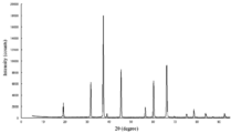
- FIG. 3 shows an XRD pattern of an inorganic compound of Example 1.
- FIG. 3 shows an excitation spectrum and an emission spectrum of the inorganic compound of Example 1.
- 1 is a schematic structural diagram of an image display device (field emission display panel) of the present invention.
- 1 is a schematic structural diagram of an image display device (liquid crystal display panel) of the present invention.
- the light-emitting device of the present invention includes at least a light-emitting light source that emits light having a wavelength of 410 nm or more and 470 nm or less, and a phosphor or a light-transmitting material in which the phosphor is dispersed.
- the phosphor is an AlON crystal, an AlON solid solution crystal, or an inorganic crystal having the same crystal structure as AlON, and at least Mn and, if necessary, an A element (provided that the A element is a monovalent metal element) And, if necessary, D element (where D element is a divalent metal element), E element (where E element is a monovalent anion) as necessary, and as necessary 515 nm by irradiating an excitation source including an inorganic compound containing G element (where G element is one or more elements other than Mn, A, Al, O, N, D, and E) To fluorescence having a peak at a wavelength in the range of 541 nm to 541 nm.
- the phosphor used for the light emitting device will be described.
- the phosphor of the present invention can contain an inorganic compound containing at least Mn as a main component in an AlON crystal, an AlON solid solution crystal, or an inorganic crystal having the same crystal structure as AlON.
- the AlON crystal is a crystal having a cubic spinel crystal structure, and is also called ⁇ -AlON (where Non-Patent Documents 1 and 2 are , Incorporated herein by reference (Theentities contents of Non-patent References 1 and 2 are incorporated here by reference.)).
- This crystal is synthesized by mixing Al 2 O 3 with AlN and firing at 1850 ° C.
- the AlON solid solution crystal is a crystal in which the oxygen / nitrogen ratio is changed while maintaining the crystal structure of AlON and / or a crystal to which other elements are added.
- Other added elements include silicon, Mg, F and the like.
- An inorganic crystal having the same crystal structure as AlON is a crystal in which a part or all of Al, O, and N are substituted with other elements while maintaining the AlON crystal structure.
- these crystals can be used as host crystals.
- An AlON crystal or an AlON solid solution crystal can be identified by X-ray diffraction or neutron diffraction. The details of the crystal structure are described in Non-Patent Documents 1 and 2, and the crystal structure and the X-ray diffraction pattern are uniquely determined from the lattice constant, space group, and atomic position data described therein.
- inorganic crystals having the same crystal structure as AlON, whose lattice constants are changed by replacing constituent elements with other elements are also the same. Identified and included as part of the present invention.
- AlON crystal, AlON solid solution crystal, or inorganic crystal having the same crystal structure as AlON is used as a base crystal, and the main component is an inorganic compound containing optically active metal element Mn. It becomes a fluorescent substance.
- the MON-containing AlON crystal, AlON solid solution crystal, or inorganic crystal having the same crystal structure as AlON is further added to an A element (provided that the A element is a monovalent metal). Since the main component is an inorganic compound containing an element), it exhibits excellent light emission characteristics. Monovalent metals are easily dissolved in the base crystal such as AlON crystal, and Mn 2+ can be stably present in the crystal to stabilize the crystal structure, and these ions are easily taken into the crystal. Become. Thereby, the brightness
- the phosphor of the present invention more preferably has the same crystal structure as AlON crystal, AlON solid solution crystal, or AlON containing Mn and A element (where A element is a monovalent metal element). Since the inorganic crystal further contains an inorganic compound containing a D element (provided that the D element is a divalent metal element) as a main component, further excellent light emission characteristics are exhibited. Divalent metal elements are easy to dissolve in a base crystal such as an AlON crystal, and in order to stabilize the crystal structure, Mn 2+ can exist stably in the crystal, and these ions are taken into the crystal. It becomes easy. Thereby, the brightness
- a composition range selected from values satisfying all of the following conditions is preferable.
- a element is a monovalent metal element
- D element is a divalent metal element
- E element is a monovalent anion element
- G element is Mn
- A, Al, O, N, D , E is one or more elements, and when the E element is two or more elements, the h value is the sum of the parameter values of the respective elements.
- the phosphor of the present invention satisfying the above composition can emit fluorescence having a peak at a wavelength in the range of 490 nm to 550 nm, specifically 515 nm to 541 nm, when irradiated with an excitation source.
- the phosphor of the present invention can emit green fluorescent light having a peak at a wavelength in the range of 518 nm or more and 530 nm or less when irradiated with an excitation source.
- the color gamut of the image display device can be expanded.
- a represents the amount of metal ion Mn that becomes the emission center, and satisfies 0.0003 ⁇ a ⁇ 0.09. If the a value is less than 0.0003, the number of ions that become the emission center is small, and the emission luminance may be reduced. If it is larger than 0.09, there is a possibility that concentration quenching occurs due to interference between ions and the luminance is lowered. More preferably, a satisfies 0.005 ⁇ a ⁇ 0.025, thereby improving the light emission luminance.
- B is the amount of element A (monovalent metal element) and satisfies 0 ⁇ b ⁇ 0.24. More preferably, b satisfies 0.02 ⁇ b ⁇ 0.09. If the b value is within this range, the emission intensity can be improved.
- the element A is Li, Na, K, etc. Among them, Li can particularly increase the emission intensity.
- C is the amount of Al element and satisfies 0.25 ⁇ c ⁇ 0.41. More preferably, c satisfies 0.31 ⁇ c ⁇ 0.41.
- the generation ratio of crystal phases other than AlON crystals, AlON solid solution crystals, or inorganic crystals having the same crystal structure as AlON increases, and the light emission intensity may decrease.
- D is the amount of oxygen, and satisfies 0.35 ⁇ d ⁇ 0.56. More preferably, d satisfies 0.4 ⁇ d ⁇ 0.56. If the d value is out of this range, the generation rate of crystal phases other than AlON crystals, AlON solid solution crystals, or inorganic crystals having the same crystal structure as AlON increases, and the light emission intensity may decrease.
- E is the amount of nitrogen and satisfies 0.02 ⁇ e ⁇ 0.13. More preferably, e satisfies 0.02 ⁇ e ⁇ 0.075. If the e value is out of this range, the generation ratio of crystal phases other than AlON crystals, AlON solid solution crystals, or inorganic crystals having the same crystal structure as AlON increases, and the light emission intensity may decrease.
- F is the amount of D element (divalent metal element) and satisfies 0 ⁇ f ⁇ 0.10. More preferably, the D element is Mg, and f satisfies 0.001 ⁇ f ⁇ 0.09. If the f value is within this range, the emission intensity can be improved.
- the element D is preferably Mg and has a particularly large effect of increasing the emission intensity.
- G is the amount of E element (monovalent anion element) and satisfies 0 ⁇ g ⁇ 0.20.
- element E fluorine, chlorine, bromine and the like can be used, and among these, F is preferable.
- F is preferable.
- element E is F
- g satisfies 0.001 ⁇ g ⁇ 0.17. If the g value is within this range, the emission intensity can be improved.
- F is particularly effective in increasing the emission intensity.
- H is the amount of one or more elements (G element) other than Mn, A, Al, O, N, D and E, and satisfies 0 ⁇ h ⁇ 0.1.
- the h value is the amount contained in or dissolved in AlON crystal, AlON solid solution crystal or inorganic crystal having the same crystal structure as AlON, and in a mixture as another crystal phase or amorphous phase. The amount contained in is not included. As long as the crystal structure of the inorganic crystal having the same crystal structure as AlON crystal, AlON solid solution crystal, or AlON is not destroyed, B, C, P, etc. can be included as the G element.
- h 0, that is, a substance that does not contain the G element has a high light emission intensity, and thus has a great effect depending on the application.
- the phosphor of the present invention satisfying the above composition can reliably emit fluorescence having a peak in a wavelength range of 515 nm to 541 nm when irradiated with an excitation source.
- the phosphor of the present invention satisfying the above composition can reliably emit green fluorescence having a peak at a wavelength in the range of 518 nm to 530 nm.
- the phosphor of the present invention irradiates light having a wavelength of 410 nm or more and 470 nm or less, preferably light having a wavelength of 420 nm or more and 460 nm or less, more preferably light having a wavelength of 430 nm or more and 460 nm or less as an excitation source. It emits green fluorescence having a peak at a wavelength in the range of 541 nm or less.
- excitation source ultraviolet rays, electron beams, X-rays and the like are preferable from the viewpoint of luminous efficiency.
- excitation is particularly efficient with light having a wavelength of 420 nm or more and 460 nm or less.
- the excitation efficiency is high at a wavelength of 430 nm to 460 nm, preferably a wavelength of 440 nm to 460 nm, more preferably a wavelength of 440 nm to 450 nm, a light emitting diode (LED) that emits light in this range and the present invention Suitable for use in white or colored LED lighting in combination with a phosphor.
- LED light emitting diode
- fluorescence having a peak at a wavelength in the range of 518 nm to 530 nm is emitted.
- the fluorescence spectrum is a sharp spectrum with a narrow line width, and emits green with good color purity. Therefore, the fluorescence spectrum is suitable for a green phosphor used for a backlight LED for liquid crystal image display elements.
- the phosphor of the present invention emits light efficiently with an electron beam, and is therefore suitable for a green phosphor for use in an image display element such as a CRT or FED excited by an electron beam.
- the inorganic compound as the main component is an AlON crystal containing at least Mn, an AlON solid solution crystal, or an inorganic crystal having the same crystal structure as AlON as much as possible with high purity from the viewpoint of fluorescence emission. If possible, it is preferably composed of a single phase, but may be a mixture with other crystalline phase or amorphous phase as long as the characteristics are not deteriorated. In this case, in order to obtain high luminance, the content of at least Mn-containing AlON crystal, AlON solid solution crystal or inorganic crystal having the same crystal structure as AlON is 10% by mass or more, more preferably 50% by mass or more. Is desirable.
- the range of the inorganic compound as the main component in the phosphor of the present invention is at least 10% by mass or more of AlON crystals containing at least Mn, AlON solid solution crystals or inorganic crystals having the same crystal structure as AlON. is there.
- X-ray diffraction measurement is performed, and the ratio of the content is obtained by performing a Rietveld analysis on the crystalline phase of the AlON crystal, the AlON solid solution crystal, or the inorganic crystal having the same crystal structure as the AlON and other crystalline phases.
- the other crystal phase or amorphous phase may be an inorganic substance having conductivity.
- the conductive inorganic material may be an oxide, oxynitride, nitride, or a mixture thereof containing one or more elements selected from Zn, Ga, In, and Sn.
- indium oxide and indium-tin oxide (ITO) are preferable because they have little decrease in fluorescence intensity and high conductivity.
- the phosphor of the present invention develops a green color, but if it is necessary to mix with other colors such as yellow and red, it may be mixed with an inorganic phosphor that develops these colors as necessary.
- Other inorganic phosphors include inorganic phosphors having a base crystal of fluoride, oxide, oxyfluoride, sulfide, oxysulfide, oxynitride, nitride crystal, etc. When durability is required, an oxynitride or nitride crystal is preferably used as a base crystal.
- Phosphors having an oxynitride or nitride crystal as a base crystal include ⁇ -sialon: Eu yellow phosphor, ⁇ -sialon: Ce blue phosphor, CaAlSiN 3 : Eu, and (Ca, Sr) AlSiN 3 : Eu red phosphor (Ca part of CaAlSiN 3 crystal substituted with Sr), blue phosphor hosting JEM phase ((LaAl (Si 6-z Al z ) N 10-z O z ): Ce ), La 3 Si 8 N 11 O 4 : Ce blue phosphor, AlN: Eu blue phosphor, and the like.
- a red phosphor having a peak in a wavelength range of 620 nm to 670 nm can be added.
- a Mn 4+ activated phosphor can be used.
- the Mn 4+ activated phosphor is preferably K 2 SiF 6 : Mn (KSF), KSNAF (K 2 Si 1 ⁇ 1 ) in which a part of constituent elements of KSF (preferably 10 mol% or less) is substituted with Al and Na.
- x Na x Al x F 6 : Mn K 2 TiF 6 : Mn (KTF), and the like.
- the phosphor of the present invention differs in excitation spectrum and fluorescence spectrum depending on the composition, and phosphors having various emission spectra can be designed by appropriately selecting and combining them. What is necessary is just to set the fluorescent substance which has the emission spectrum required based on a use.
- the phosphor production method of the present invention includes an AlON-containing raw material selected from the group consisting of AlON crystals, AlON solid solution crystals, or inorganic crystals having the same crystal structure as AlON, a raw material containing Mn, and Accordingly, a raw material containing Li is mixed and heat-treated at a temperature of 1500 ° C. to 1900 ° C. in a nitrogen atmosphere of 0.2 to 100 atm. Thereby, the Mn content in the AlON-containing raw material can be increased.
- the AlON-containing raw material may be an AlON crystal, an AlON solid solution crystal, or an inorganic crystal having the same crystal structure as that of AlON.
- an A element, a D element, an E element, G element and Mn may be contained.
- a raw material containing Al a raw material containing an A element (where A element is a monovalent metal element) as required, and a D element (where D element is a divalent metal element, if necessary)
- a raw material containing Mn a raw material containing Mn as required.
- the A element is Li and the D element is Mg.
- the raw material containing Al is selected from the group consisting of metallic aluminum, aluminum oxide, aluminum nitride, and an organic precursor containing aluminum.
- a mixture of aluminum nitride and aluminum oxide is used.
- the amount of aluminum nitride and aluminum oxide may be designed from the ratio of oxygen and nitrogen having a target AlON composition.
- the raw material containing element D is selected from the group consisting of metals, oxides, carbonates, nitrides, fluorides, chlorides, oxynitrides, and combinations thereof of element D.
- the raw material containing the element D can be added with a magnesium-containing metal, oxide, carbonate, nitride, fluoride, chloride, oxynitride or a combination thereof, Preferred are magnesium oxide and magnesium carbonate. In addition to being able to obtain a highly pure synthetic product with high reactivity, these have the advantage that they are produced as industrial raw materials and are easily available.
- the raw material containing the A element is A nitride, carbonate, fluoride or the like.
- the raw material containing the A element is selected from the group consisting of lithium nitride, lithium carbonate, and lithium fluoride.
- the raw material containing Mn is selected from the group consisting of Mn metal, oxide, carbonate, nitride, fluoride, chloride, oxynitride, and combinations thereof.
- the raw material containing Mn is manganese monoxide, manganese dioxide, or manganese carbonate. In addition to being able to obtain a highly pure synthetic product with high reactivity, these have the advantage that they are produced as industrial raw materials and are easily available.
- Optimized firing temperature may vary depending on the composition and can be optimized as appropriate. When the firing temperature is lower than 1600 ° C., the generation rate of AlON crystals, AlON solid solution crystals, or inorganic crystals having the same crystal structure as AlON may be low. Further, when the firing temperature is 2400 ° C. or higher, a special apparatus is required, which is not industrially preferable.
- an inorganic compound that generates a liquid phase at a temperature lower than the firing temperature can be added to the raw material mixture as necessary.
- the inorganic compound those that generate a stable liquid phase at the reaction temperature are preferable, and fluorides, chlorides, iodides, bromides, or phosphates of Li, Na, K, Mg, Ca, Sr, Ba, and Al are used. Is suitable.
- these inorganic compounds may be added alone or in combination of two or more.
- magnesium fluoride, aluminum fluoride, and lithium fluoride are preferable because they improve the reactivity of synthesis.
- the addition amount of the inorganic compound is not particularly limited, but a range of 0.1 to 10 parts by weight with respect to 100 parts by weight of the raw material mixture is preferable because the reactivity is improved. If the amount is less than 0.1 parts by weight, the reactivity is not improved, and if it exceeds 10 parts by weight, the luminance of the phosphor may be lowered.
- these inorganic compounds are added to the raw material mixture and baked, the reactivity is improved, grain growth is promoted in a relatively short time, a single crystal having a large grain size grows, and the brightness of the phosphor is improved. .
- the nitrogen atmosphere is preferably a gas atmosphere having a pressure range of 0.2 to 100 atm. Heating to a temperature of 2400 ° C. or higher in a nitrogen gas atmosphere lower than 0.2 atm is not preferable because the raw material is likely to be thermally decomposed. If it exceeds 100 atmospheres, a special device is required, which is not suitable for industrial production.
- the mixed raw material mixture has a form in which fine powder having a particle size of several ⁇ m is aggregated to a size of several hundred ⁇ m to several mm (hereinafter referred to as “powder agglomeration”). Called “collection”).
- the powder aggregate is fired in a state where the bulk density is maintained at a filling rate of 40% or less. More preferably, the bulk density is 20% or less.
- the relative bulk density is a ratio of a value (bulk density) obtained by dividing the mass of the powder filled in the container by the volume of the container and the true density of the substance of the powder.
- a hot press method in which heating is performed while applying pressure or a production method in which baking is performed after mold forming (compacting) is used, but the firing at this time is performed with a high powder filling rate.
- the powder aggregates of the raw material mixture having the same particle size are left as they are.
- a container is filled with a bulk density of 40% or less. If necessary, the particle size can be controlled by granulating the powder aggregate to an average particle size of 500 ⁇ m or less using a sieve or air classification.
- the container may be granulated directly into a shape having an average particle diameter of 500 ⁇ m or less using a spray dryer or the like. Further, when the container is made of boron nitride, there is an advantage that there is little reaction with the phosphor.
- the reason why firing is performed while maintaining the bulk density at 40% or less is because firing is performed in a state where there is a free space around the raw material powder.
- the optimum bulk density varies depending on the shape and surface state of the granular particles, but is preferably 20% or less. In this way, the reaction product grows in a free space, so that the contact between the crystals is reduced and a crystal with few surface defects can be synthesized. Thereby, a fluorescent substance with high brightness is obtained. If the bulk density exceeds 40%, partial densification occurs during firing, resulting in a dense sintered body, which may hinder crystal growth and reduce the brightness of the phosphor. Moreover, it is difficult to obtain a fine powder.
- a powder aggregate having an average particle size of 500 ⁇ m or less is particularly preferable because of excellent crushability after firing.
- the furnace used for firing may be a metal resistance heating method or a graphite resistance heating method because the firing temperature is high and the firing atmosphere is nitrogen.
- An electric furnace using carbon as the material for the high temperature part of the furnace is preferred.
- the firing is preferably performed by a firing method in which no mechanical pressure is applied from the outside, such as an atmospheric pressure sintering method or a gas pressure sintering method, in order to perform the firing while maintaining a bulk density in a predetermined range.
- the powder aggregate obtained by firing is agglomerated tightly, it is pulverized by a pulverizer generally used in industry such as a ball mill and a jet mill.
- a pulverizer generally used in industry such as a ball mill and a jet mill.
- ball milling makes it easy to control the particle size.
- the balls and pots used at this time are preferably made of a silicon nitride sintered body or a sialon sintered body. Grinding is performed until the average particle size becomes 20 ⁇ m or less.
- the average particle size is particularly preferably 5 ⁇ m or more and 20 ⁇ m or less.
- the average particle diameter exceeds 20 ⁇ m, the fluidity of the powder and the dispersibility in the resin are deteriorated, and the light emission intensity becomes uneven depending on the part when the light emitting device is formed in combination with the light emitting element. If it is 5 ⁇ m or less, the luminous efficiency of the phosphor may be lowered. If the desired particle size cannot be obtained only by grinding, classification can be combined. As a classification method, sieving, air classification, precipitation in a liquid, or the like can be used.
- the content of inorganic compounds other than phosphors such as glass phase, second phase, or impurity phase contained in the reaction product obtained by firing is reduced.
- a solvent water and an aqueous solution of an acid can be used.
- the acid aqueous solution sulfuric acid, hydrochloric acid, nitric acid, hydrofluoric acid, a mixture of organic acid and hydrofluoric acid, or the like can be used. Of these, a mixture of sulfuric acid and hydrofluoric acid is highly effective. This treatment is particularly effective for a reaction product obtained by adding an inorganic compound that generates a liquid phase at a temperature lower than the firing temperature and firing at a high temperature.
- the raw material containing Mn and the raw material containing Li as necessary are added to the AlON-containing raw material, Heat treatment is performed in a temperature range of 1500 ° C. to 1900 ° C. in a nitrogen atmosphere of 0.2 atm or more and 100 atm or less.
- the AlON-containing raw material stably dissolves Mn in AlON crystals, AlON solid solution crystals, or inorganic crystals having the same crystal structure as AlON, and further increases the Mn content contained in these crystals. effective.
- the emission intensity is improved.
- variation in light emission characteristics among production lots can be reduced and yield can be improved.
- the AlON-containing raw material is produced by the above-described method for producing an AlON-containing raw material, in addition to Mn, it may contain an A element, a D element, an E element, and a G element.
- the AlON-containing raw material is an AlON solid solution crystal, and the AlON solid solution crystal contains one or more elements selected from the group consisting of Mn, Eu, Mg and Li, and similarly contains Mn. The amount can be increased.
- the synthesis of AlON crystals, AlON solid solution crystals, or inorganic crystals having the same crystal structure as AlON is performed at a high temperature of 1800 ° C. or higher, more preferably 1900 ° C. or higher from the viewpoint of reaction rate. In order to increase the particle size, a high temperature of 2000 ° C. or higher is desirable.
- the vapor pressure of Mn is high, the Mn content in AlON crystals, AlON solid solution crystals, or inorganic crystals having the same crystal structure as AlON decreases when heat-treated at a high temperature of 1800 ° C. or higher for a long time. There is. When the Mn content decreases, the luminance of the phosphor decreases and the light emission characteristics vary from lot to lot.
- an AlON phosphor having a Mn content necessary for light emission and high luminance can be synthesized as compared with an AlON phosphor obtained by a conventional synthesis method.
- a raw material containing Mn used in the production of the above-described AlON-containing raw material can be adopted.
- a raw material containing Li As a raw material containing Li, a raw material containing an A element (when the A element is Li) used in the production of the above-described AlON-containing raw material can be adopted. From the viewpoint of reactivity, lithium fluoride and / or Or it may be lithium nitride.
- the MON content in the AlON-containing raw material is 0.5 atomic%. It is preferable to carry out until it becomes above. Thereby, a phosphor with improved light emission luminance can be obtained.
- an AlON-containing raw material is mixed with aluminum oxide and aluminum nitride as a raw material containing Al, a raw material containing a D element as required, and a raw material containing an A element as needed.
- the raw material containing Al and the raw material containing D element (not including A element), or the raw material containing Al and the raw material containing A element (not including D element) can be used.
- the mixed raw materials are calcined in a temperature range of 1800 ° C. to 2400 ° C., preferably 1900 ° C. to 2200 ° C., in a nitrogen atmosphere of 0.2 to 100 atm.
- the D element and the A element may be Mg and Li.
- highly crystalline AlON crystals, AlON solid solution crystals, or inorganic crystals having the same crystal structure as AlON are obtained.
- the synthesized AlON-containing raw material is mixed with manganese fluoride as a raw material containing Mn and, if necessary, lithium fluoride as a raw material containing element A, and heat-treated in a temperature range of 1500 ° C. or higher and 1850 ° C. or lower. To do.
- Mn may not be sufficiently dissolved in an AlON crystal, an AlON solid solution crystal, or an inorganic crystal having the same crystal structure as AlON.
- the content of inorganic compounds other than phosphors such as glass phase, second phase, or impurity phase contained in the reaction product obtained by firing is reduced.
- a solvent water and an aqueous solution of an acid can be used.
- the acid aqueous solution sulfuric acid, hydrochloric acid, nitric acid, hydrofluoric acid, a mixture of organic acid and hydrofluoric acid, or the like can be used. Of these, a mixture of sulfuric acid and hydrofluoric acid is highly effective. This treatment is particularly effective for a reaction product obtained by adding an inorganic compound that generates a liquid phase at a temperature lower than the firing temperature and firing at a high temperature.
- the powder after baking or the powder after particle size adjustment by pulverization or classification may be heat-treated at a temperature of 1000 ° C. or higher and lower than the baking temperature. At a temperature lower than 1000 ° C., the effect of removing surface defects is small. Above the firing temperature, the pulverized powders are fixed again, which is not preferable.
- the atmosphere suitable for the heat treatment varies depending on the composition of the phosphor, but one or two or more mixed atmospheres selected from the group consisting of nitrogen, air, ammonia and hydrogen can be used, and the nitrogen atmosphere is particularly defective. It is preferable because of its excellent removal effect.
- the phosphor of the present invention obtained as described above is characterized by having high-luminance visible light emission as compared with a normal oxide phosphor or an existing AlON phosphor.
- a specific composition is characterized by emitting green light, and is suitable for a light emitting device and an image display device.
- it since it does not deteriorate even when exposed to high temperatures, it has excellent heat resistance, and excellent long-term stability in an oxidizing atmosphere and moisture environment.
- the light-emitting device of the present invention includes at least a light-emitting source that emits light having a wavelength of 410 nm or more and 470 nm or less, and the above-described phosphor or a light-transmitting material in which the phosphor is dispersed.
- Examples of light emitting devices include LED lighting devices and LD (laser diode) lighting devices.
- An LED lighting apparatus is manufactured by using the phosphor of the present invention by a known method as described in JP-A-5-152609, JP-A-7-99345, JP-A-2927279, and the like. Can do. In this case, it is desirable that the light emission source emits light having a wavelength of 410 nm or more and 470 nm or less, and among them, an LED light emitting element or an LD light emitting element that emits light having a peak in a wavelength range of 430 nm or more and 470 nm or less is preferable.
- the phosphor of the present invention can emit light with high brightness.
- these light emitting elements include those made of nitride semiconductors such as GaN and InGaN, and can be light emitting light sources that emit light of a predetermined wavelength by adjusting the composition.
- a light emitting device that emits a desired color can be configured by using it together with a phosphor having other light emission characteristics.
- a phosphor having other light emission characteristics there is a combination of a 445 nm blue LED or LD light emitting element, a yellow phosphor excited at this wavelength and having an emission peak at a wavelength of 550 nm to 600 nm and a green phosphor of the present invention.
- ⁇ -sialon Eu 2+ described in JP-A No. 2002-363554 and (Y, Gd) 2 (Al, Ga) 5 O 12 described in JP-A No.
- Ce can be mentioned. In this configuration, when blue light emitted from the LED or LD is irradiated onto the phosphor, blue, green, and yellow light is emitted, and a white light emitting device is obtained by mixing these.
- a combination of a 445 nm blue LED or LD light emitting element, a red phosphor having an emission peak at a wavelength of 620 nm or more and 670 nm or less excited at this wavelength, and the green phosphor of the present invention examples include CaSiAlN 3 : Eu 2+ and KSF or KSNAF described in International Publication No. 2005/052087 pamphlet.
- red and green light is emitted, and a white light emitting device is obtained by mixing the blue light and the light from the phosphor.
- the light transmitting body in which the phosphor containing at least the phosphor of the present invention is dispersed is selected from the group consisting of acrylic resin, silicone resin and glass. These materials are excellent in translucency with respect to the light from the light emitting light source described above, and can excite the phosphor of the present invention with high efficiency.
- the ratio of the phosphor in the light transmitting body in which the phosphor containing the phosphor of the present invention is dispersed is preferably in the range of 30% by volume to 90% by volume. Thereby, the phosphor of the present invention can be excited with high efficiency.
- the image display device of the present invention uses the above-described light emitting device as a backlight.
- Such an image display device is, for example, a liquid crystal display (LCD) such as a liquid crystal television or a portable terminal.
- LCD liquid crystal display
- the above-described light-emitting device employs the above-described phosphor as a component that emits green light with a sharp spectrum, and thus provides a liquid crystal panel with a wide color space (color gamut) that can be reproduced by a liquid crystal display and good color reproducibility. can do.
- Another image display device of the present invention includes at least an excitation source and a phosphor, and the phosphor includes at least the phosphor of the present invention described above.
- the image display device include a fluorescent display tube (VFD), a field emission display (FED or SED), a plasma display panel (PDP), and a cathode ray tube (CRT).
- the phosphor of the present invention has been confirmed to emit light by excitation of vacuum ultraviolet rays of 100 to 190 nm, ultraviolet rays of 190 to 380 nm, electron beams, etc., and in combination of these excitation sources and the phosphor of the present invention, An image display apparatus as described above can be configured.
- the phosphor of the present invention is suitable for VFD, SED, PDP, and CRT applications that are used at an acceleration voltage of 10 V or more and 30 kV or less because it is highly efficient by an electron beam and excellent in excitation excitation efficiency.
- the FED is an image display device that emits light by accelerating electrons emitted from a field emission cathode and colliding with a phosphor applied to the anode, and is required to emit light at a low acceleration voltage of 5 kV or less. By combining these phosphors, the light emission performance of the display device is improved.
- an aluminum nitride powder (F grade made by Tokuyama) with a specific surface area of 3.3 m 2 / g and an oxygen content of 0.79%, and an aluminum oxide powder with a specific surface area of 13.6 m 2 / g and a purity of 99.99% (Daiming Chemical's Tymicron grade), lithium carbonate powder (high purity chemical reagent grade), LiAlO 2 powder, purity 99.9% lithium fluoride powder (high purity scientific reagent grade), purity 99 9% manganese fluoride powder (high purity chemical reagent grade) and 99.99% pure magnesium oxide (high purity chemical reagent grade) were used.
- AlON-containing raw material powder was synthesized.
- Aluminum oxide, aluminum nitride, and, if necessary, magnesium oxide, lithium carbonate, and LiAlO 2 were weighed so as to have the design composition shown in Table 1.
- aluminum oxide, aluminum nitride, and magnesium oxide were weighed in proportions of 83.85% by mass, 11.24% by mass, and 4.91% by mass, respectively.
- a powder aggregate having excellent fluidity was obtained by passing through a sieve having an opening of 125 ⁇ m.
- the crucible was set in a graphite resistance heating type electric furnace.
- the firing atmosphere is evacuated by a diffusion pump, heated from room temperature to 800 ° C. at a rate of 600 ° C. per hour, introduced with nitrogen having a purity of 99.9995 vol% at 800 ° C. and a gas pressure of 4.
- the pressure was 5 atm and the temperature was raised to 600 ° C. per hour up to the temperature shown in Table 1 (for example, 2000 ° C. in Example 1) and maintained at that temperature for the time shown in Table 1 (for example, 2 hours in Example 1).
- the synthesized sample was pulverized using a silicon nitride mortar and pestle and passed through a sieve having an opening of 125 ⁇ m.
- the crucible was set in a graphite resistance heating type electric furnace.
- the firing atmosphere is evacuated by a diffusion pump, heated from room temperature to 800 ° C. at a rate of 600 ° C. per hour, introduced with nitrogen having a purity of 99.9995 vol% at 800 ° C. and a gas pressure of 4.
- the pressure was 5 atm
- the temperature was raised to 600 ° C. per hour up to the temperature shown in Table 2 (for example, 1700 ° C. in Example 1), and the temperature shown in Table 2 (for example, 2 hours in Example 1) was maintained.
- the synthesized sample was pulverized using a mortar and pestle made of silicon nitride.
- the samples of Examples 1, 4, 9 to 28 include Al, N, Li, Mn, Mg, F, and O, and the samples of Examples 2 and 3 are Al, N, Li, Mn, F It was confirmed that the samples of Examples 5 to 8 contained Al, N, Mn, Mg, F and O. Further, powder X-ray diffraction measurement (XRD) using Cu K ⁇ rays was performed on the synthesized samples. The results are shown in FIG.
- FIG. 1 is a diagram showing an XRD pattern of the inorganic compound of Example 1.
- FIG. 1 is a diagram showing an XRD pattern of the inorganic compound of Example 1.
- a ⁇ -type AlON structure crystal and a second phase of aluminum oxide or aluminum nitride were confirmed. From the ratio of the height of the main peak, the production ratio of crystals having a ⁇ -type AlON structure was determined to be 90% or more. In addition, the peak which shows the compound of Li was not detected.
- the XRD patterns of the other examples were the same.
- the samples obtained in the examples were mainly composed of an inorganic compound containing an AlON crystal containing at least Mn and further Li, Mg, or F. Among them, Mn, Li, F and It was found that Mg was dissolved in the AlON crystal.
- the sample obtained in the example is a phosphor that has an inorganic compound containing an AlON crystal containing at least Mn, and optionally contains Li, Mg, and F, and emits green light. Indicated.
- FIG. 2 is a diagram showing an excitation spectrum and an emission spectrum of the inorganic compound of Example 1.
- FIG. 2 shows an emission spectrum when excited at a wavelength of 447 nm and an excitation spectrum when the emission wavelength is fixed at 524 nm.
- the excitation spectrum of FIG. 2 it was confirmed that the inorganic compound of Example 1 was excited by light having a wavelength of 410 nm or more and 470 nm or less.
- Table 3 it was found that the inorganic compound of Example 1 was most excited at 447 nm and emitted green light having a peak at a wavelength of 524 nm.
- the inorganic compounds of Examples 1 to 28 have an excitation spectrum peak at a wavelength of 420 nm to 450 nm, and emit fluorescence having a peak at a wavelength in the range of 490 nm to 550 nm in excitation at the peak wavelength of the excitation spectrum.
- the phosphor emits high-luminance light having a peak at a wavelength in the range of 515 nm to 541 nm, preferably 518 nm to 530 nm.
- the emission characteristics (cathode luminescence, CL) when irradiated with an electron beam were observed with a SEM equipped with a CL detector, and the CL image was evaluated. As a result, it was confirmed that the inorganic compounds of all the examples were excited by an electron beam and emitted green light.
- Example 29 In Example 29, an AlON phosphor was directly synthesized without passing through an AlON-containing raw material. In Example 29, a LiON-free AlON phosphor having the same design composition as Example 5 in Table 2 was synthesized.
- Example 2 In the same manner as the procedure for synthesizing the AlON-containing raw material of Example 1 by mixing aluminum nitride, aluminum oxide, magnesium oxide and manganese fluoride so as to have the same design composition as Example 5 of Table 2, 2000 ° C. For 2 hours.
- the emission spectrum and excitation spectrum of the inorganic compound of Example 29 obtained in this manner were measured using a fluorescence spectrophotometer. As a result, the inorganic compound of Example 29 emitted green light, but its emission intensity was lower than that of Examples 1 to 28.
- FIG. 3 shows a schematic structural diagram of the light-emitting device (white LED light-emitting device) of the present invention.
- the white LED of the present invention includes a phosphor mixture 1 including the phosphor of the present invention and other phosphors, and a light emission source 2.
- the phosphor mixture 1 was a mixture of the green phosphor manufactured in Example 1 of the present invention and a red phosphor of CaAlSiN 3 : Eu.
- the light emission source 2 is a light emitting element made of a 445 nm blue LED chip.
- the phosphor mixture 1 was dispersed in the resin layer 6 and covered with the blue LED chip 2, and was placed in the container 7.
- the current is supplied to the blue LED chip 2 through the wire bond 5, and 445 nm light is emitted.
- the phosphor mixture 1 of the green phosphor and the red phosphor is generated by this light. When excited, it emits green and red light, respectively.
- the green light, the red light, and the blue light from the blue LED chip 2 were mixed to function as a light emitting device that emits white light.
- the phosphor mixture 1, the green phosphor and K 2 SiF 6 produced in Example 1 Using the Mn red fluorescent material, to constitute a light-emitting device of FIG. Also in this case, in the light emitting device of the present invention, the phosphor mixture 1 of the green phosphor and the red phosphor is excited by the light of 445 nm emitted from the blue LED chip 2, and emits green and red light, respectively. The green light, the red light, and the blue light from the blue LED chip 2 were mixed to function as a light emitting device that emits white light.
- FIG. 4 is a schematic structural diagram of the image display device (field emission display panel) of the present invention.
- the image display device of the present invention includes at least an emitter 55 as an excitation source and the green phosphor 56 manufactured in Example 1.
- the green phosphor 56 is applied to the inner surface of the anode 53.
- By applying a voltage between the cathode 52 and the gate 54 electrons 57 are emitted from the emitter 55.
- the electrons 57 are accelerated by the voltage between the anode 53 and the cathode 52, collide with the green phosphor 56, and emit green light.
- the entire image display device of the present invention is protected by glass 51.
- one light emitting cell composed of one emitter and one phosphor is shown, but in reality, in addition to green, a large number of blue and red cells are arranged to display various colors. Composed. Although it does not specify in particular about the fluorescent substance used for a blue or red cell, what emits high brightness
- FIG. 5 is a schematic structural diagram of the image display device (liquid crystal display panel) of the present invention.
- the liquid crystal display panel includes an optical shutter portion including a polarizing filter 71, transparent electrodes 73 to 77, and a liquid crystal (liquid crystal molecular layer) 78, and a backlight light source 70.
- a white LED having the structure shown in FIG. 3 is used as the backlight light source 70.
- a phosphor mixture 1 containing the phosphor of the present invention and other phosphors and a blue LED chip 2 having a wavelength of 450 nm are used as a light emitting element.
- a phosphor mixture 1 in which a green phosphor manufactured in Example 1 of the present invention and a red phosphor (K 2 SiF 6 : Mn red phosphor) as another phosphor are dispersed in a resin layer 6 is used as a blue LED chip. 2 and is placed in the container 7.
- a current is passed through the conductive terminals 3 and 4
- a current is supplied to the blue LED chip 2 through the wire bond 5, and 450 nm light is emitted.
- the phosphor mixture 1 of the green phosphor and the red phosphor is formed. Excited to emit green and red light, respectively, and blue light emitted from the blue LED chip 2 is mixed to emit white light.
- this white LED chip is used as an LED backlight 70 for a backlight light source.
- the mixed light of red, green and blue emitted from the LED backlight 70 passes through the polarizing filter 71, the glass substrate 72 and the transparent electrode 73 and reaches the liquid crystal molecular layer 78.
- the direction of the liquid crystal molecules present in the liquid crystal molecule layer 78 changes depending on the voltage between the transparent electrode 73 as a common electrode and the transparent electrodes 75, 76, 77 for displaying each color of red, green, and blue disposed on the pixel electrode 74.
- the light transmittance changes.
- the light that has passed through the transparent electrodes 75, 76, 77 is emitted to the outside through the red, green, and blue color filters 79, 80, 81, the glass substrate 72, and the polarizing filter 71. In this way, an image is displayed.
- the backlight light source 70 is composed of blue, green, and red light components having a sharp spectrum and has good light separation characteristics when separated by the polarizing filter 71, the separated light has chromaticity.
- the color purity of chromaticity points of red, green, and blue on the coordinates is improved.
- a color space (color gamut) that can be reproduced by the liquid crystal display is widened, and a liquid crystal panel having good color reproducibility can be provided.
- the phosphor of the present invention emits green light with good color purity, and further, since the luminance of the phosphor does not decrease significantly when exposed to an excitation source, it is suitable for VFD, FED, PDP, CRT, white LED, etc. Can be used. In the future, it is expected to contribute greatly to industrial development by being widely used in backlight LEDs and various display devices excited by electron beams.
Landscapes
- Chemical & Material Sciences (AREA)
- Engineering & Computer Science (AREA)
- Inorganic Chemistry (AREA)
- Organic Chemistry (AREA)
- Materials Engineering (AREA)
- Physics & Mathematics (AREA)
- Optics & Photonics (AREA)
- Electromagnetism (AREA)
- General Engineering & Computer Science (AREA)
- Microelectronics & Electronic Packaging (AREA)
- Plasma & Fusion (AREA)
- Luminescent Compositions (AREA)
- Cathode-Ray Tubes And Fluorescent Screens For Display (AREA)
- Led Device Packages (AREA)
Abstract
Description
前記蛍光体は、組成式MnaAbAlcOdNeDfEgGh(ただし、式中a+b+c+d+e+f+g+h=1とする)で示され、パラメータa、b、c、d、e、f、gおよびhは、
0.0003≦ a ≦0.09
0≦ b ≦0.24
0.25≦ c ≦0.41
0.35≦ d ≦0.56
0.02≦ e ≦0.13
0≦ f ≦0.10
0≦ g ≦0.20および
0≦ h ≦0.10
を満たしてもよい。
前記A元素はLiであり、前記パラメータaは、0.005≦ a ≦0.025を満たしてもよい。
前記D元素はMgであり、前記パラメータfは、0.001≦ f ≦0.09を満たしてもよい。
前記E元素がFであり、前記パラメータgは、0.001≦ g ≦0.17を満たしてもよい。
前記パラメータhは、h=0を満たしてもよい。
前記発光光源は、430~460nmの範囲の波長にピークを持つ光を発するLED(発光ダイオード)またはLD(レーザダイオード)であってもよい。
前記発光光源は、440~460nmの範囲の波長にピークを持つ光を発するLED(発光ダイオード)またはLD(レーザダイオード)であり、蛍光体が励起源を照射することにより518nm以上530nm以下の範囲の波長にピークを有する蛍光を発してもよい。
前記蛍光体は、620nm以上670nm以下の範囲の波長にピークを有する赤色蛍光体をさらに含んでもよい。
前記赤色蛍光体は、Mn4+付活蛍光体であってもよい。
前記赤色蛍光体は、KSFおよび/またはKSNAFであってもよい。
本発明の画像表示装置は、少なくとも上述の発光器具をバックライトとして用い、これにより上記課題を解決する。
本発明の発光器具は、少なくとも、410nm以上470nm以下の波長の光を発する発光光源と、蛍光体または蛍光体が分散した光透過体とを備える。ここで、上記蛍光体は、AlON結晶、AlON固溶体結晶、または、AlONと同一の結晶構造を有する無機結晶に、少なくともMnと、必要に応じてA元素(ただし、A元素は1価の金属元素である)と、必要に応じてD元素(ただし、D元素は2価の金属元素である)と、必要に応じてE元素(ただし、E元素は1価のアニオン)と、必要に応じてG元素(ただし、G元素はMn、A、Al、O、N、D、E以外の1種または2種以上の元素)とを含有する無機化合物を含み、励起源を照射することにより、515nmから541nmの範囲の波長にピークを持つ蛍光を発する。
本発明の蛍光体は、AlON結晶、AlON固溶体結晶、または、AlONと同一の結晶構造を有する無機結晶に、少なくともMnを含有する無機化合物を主成分として含むことができる。
0.0003≦ a ≦0.09
0≦ b ≦0.24
0.25≦ c ≦0.41
0.35≦ d ≦0.56
0.02≦ e ≦0.13
0≦ f ≦0.10
0≦ g ≦0.20および
0≦ h ≦0.10
上記組成を満たす本発明の蛍光体は、励起源を照射すると、490nm以上550nm以下、詳細には515nm以上541nm以下の範囲の波長にピークを有する蛍光を発することができる。さらに組成を制御することにより、本発明の蛍光体は、励起源を照射すると、518nm以上530nm以下の範囲の波長にピークを有する色純度のよい緑色の蛍光を発することができるので、発光器具および画像表示装置の色域を広げることができる。
0.005≦ a ≦0.025
0≦ b ≦0.16
0.26≦ c ≦0.39
0.35≦ d ≦0.52
0.03≦ e ≦0.055
0≦ f ≦0.03および
0.01 ≦g ≦ 0.18
を満たす。これにより、上記組成を満たす本発明の蛍光体は、励起源を照射すると、515nm以上541nm以下の範囲の波長にピークを有する蛍光を確実に発することができる。
0.005< a <0.02
0.02≦ b ≦0.12
0.28≦ c ≦0.37
0.38≦ d ≦0.52
0.04≦ e ≦0.055
0.018≦ f ≦0.024および
0.02 ≦g ≦ 0.15
を満たす。これにより、上記組成を満たす本発明の蛍光体は、518nm以上530nm以下の範囲の波長にピークを有する色純度のよい緑色の蛍光を確実に発することができる。
本発明の蛍光体の製造方法は、AlON結晶、AlON固溶体結晶、または、AlONと同一の結晶構造を有する無機結晶からなる群から選択されるAlON含有原料と、Mnを含有する原料と、必要に応じてLiを含有する原料とを混合し、0.2気圧以上100気圧以下の窒素雰囲気中で、1500℃以上1900℃以下の温度で熱処理する。これにより、AlON含有原料中のMn含有量を増加させることができる。なお、AlON含有原料は、AlON結晶、AlON固溶体結晶、または、AlONと同一の結晶構造を有する無機結晶であってもよいし、これらに、必要に応じて、A元素、D元素、E元素、G元素、Mnが含有されていてもよい。
Alを含有する原料と、必要に応じてA元素(ただし、A元素は1価の金属元素である)を含有する原料と、必要に応じてD元素(ただし、D元素は2価の金属元素である)を含有する原料と、必要に応じてMnを含有する原料とを準備する。例えば、A元素はLiであり、D元素はMgである。
まず、AlON含有原料を、Alを含有する原料として酸化アルミニウムおよび窒化アルミニウムと、必要に応じてD元素を含有する原料と、必要に応じてA元素を含有する原料とを混合する。ここで、前記Alを含有する原料とD元素を含有する原料(A元素を含まない)、或いは、前記Alを含有する原料とA元素を含有する原料(D元素を含まない)することができる。このように混合した原料を、0.2気圧以上100気圧以下の範囲の窒素雰囲気中で、1800℃以上2400℃以下の温度範囲、好ましくは、1900℃以上2200℃以下の温度範囲で焼成す。これによってAlON含有原料を合成する。ここで、D元素およびA元素は、MgおよびLiであってよい。1900℃以上2200℃以下の温度範囲で焼成すれば、結晶性の高いAlON結晶、AlON固溶体結晶、または、AlONと同一の結晶構造を有する無機結晶が得られる。
原料粉末として、比表面積3.3m2/g、酸素含有量0.79%の窒化アルミニウム粉末(トクヤマ製Fグレード)と、比表面積13.6m2/g、純度99.99%の酸化アルミニウム粉末(大明化学製タイミクロングレード)と、炭酸リチウム粉末(高純度化学製試薬級)と、LiAlO2粉末と、純度99.9%のフッ化リチウム粉末(高純度科学製試薬級)と、純度99.9%のフッ化マンガン粉末(高純度化学製試薬級)と、純度99.99%の酸化マグネシウム(高純度化学製試薬級)とを用いた。
まず、AlON含有原料粉末を合成した。表1に示す設計組成になるように、酸化アルミニウムと、窒化アルミニウムと、必要に応じて、酸化マグネシウムと、炭酸リチウムと、LiAlO2とを秤量した。例えば、実施例1の場合には、酸化アルミニウム、窒化アルミニウム、および、酸化マグネシウムを、それぞれ、83.85質量%、11.24質量%、および、4.91質量%の割合で秤量した。窒化ケイ素焼結体製の乳鉢と乳棒とを用いて原料を混合した後に、目開き125μmのふるいを通すことにより流動性に優れる粉体凝集体を得た。この粉体凝集体を直径20mm高さ20mmの大きさの窒化ホウ素製るつぼに自然落下させて入れたところ、嵩密度は30体積%であった。嵩密度は、投入した粉体凝集体の重量とるつぼの内容積と粉体の真密度とから計算した。
表2に示す設計組成となるように、合成したAlON含有原料粉末と、MnF2粉末と、LiF粉末とを秤量した。例えば、実施例1の場合には、AlON含有原料粉末、MnF2粉末、および、LiF粉末を、それぞれ、2g、0.16g、および、0.2gを満たす質量比で秤量した。窒化ケイ素焼結体製の乳鉢と乳棒とを用いて原料を混合した後に、目開き125μmのふるいを通したものを、直径20mm高さ20mmの大きさの窒化ホウ素製るつぼに自然落下させて入れた。


実施例29では、AlON含有原料を経ることなく、直接AlON蛍光体を合成した。実施例29では、表2の実施例5と同じ設計組成を有するLiを含まないAlON蛍光体を合成した。
図3は、本発明の発光器具(白色LED発光器具)の概略構造図を示す。
図4は、本発明の画像表示装置(フィールドエミッションディスプレイパネル)の概略構造図である。
図5は、本発明の画像表示装置(液晶ディスプレイパネル)の概略構造図である。
2 青色LEDチップ
3、4 導電性端子
5 ワイヤーボンド
6 樹脂層
7 容器
51 ガラス
52 陰極
53 陽極
54 ゲート
55 エミッタ
56 蛍光体
57 電子
70 LEDバックライト(バックライト光源)
71 偏光フィルタ
72 ガラス基板
73 透明電極(共通電極)
74 透明電極(画素電極)
75 透明電極(赤表示用)
76 透明電極(緑表示用)
77 透明電極(青表示用)
78 液晶分子層
79 カラーフィルタ(赤表示用)
80 カラーフィルタ(緑表示用)
81 カラーフィルタ(青表示用)
Claims (12)
- 少なくとも、410nm以上470nm以下の波長の光を発する発光光源と、蛍光体または蛍光体が分散した光透過体とを備える発光器具であって、
前記蛍光体は、AlON結晶、AlON固溶体結晶、または、AlONと同一の結晶構造を有する無機結晶に、少なくともMnと、必要に応じてA元素(ただし、A元素は1価の金属元素である)と、必要に応じてD元素(ただし、D元素は2価の金属元素である)と、必要に応じてE元素(ただし、E元素は1価のアニオン)と、必要に応じてG元素(ただし、G元素はMn、A、Al、O、N、D、E以外の1種または2種以上の元素)とを含有する無機化合物を含み、励起源を照射することにより、515nmから541nmの範囲の波長にピークを持つ蛍光を発する、発光器具。 - 前記蛍光体は、組成式MnaAbAlcOdNeDfEgGh(ただし、式中a+b+c+d+e+f+g+h=1とする)で示され、パラメータa、b、c、d、e、f、gおよびhは、
0.0003≦ a ≦0.09
0≦ b ≦0.24
0.25≦ c ≦0.41
0.35≦ d ≦0.56
0.02≦ e ≦0.13
0≦ f ≦0.10
0≦ g ≦0.20および
0≦ h ≦0.10
を満たす、請求項1に記載の発光器具。 - 前記A元素はLiであり、
前記パラメータaは、0.005≦ a ≦0.025を満たす、請求項2に記載の発光器具。 - 前記D元素はMgであり、
前記パラメータfは、0.001≦ f ≦0.09を満たす、請求項2に記載の発光器具。 - 前記E元素がFであり、
前記パラメータgは、0.001≦ g ≦0.17を満たす、請求項2に記載の発光器具。 - 前記パラメータhは、h=0を満たす、請求項2に記載の発光器具。
- 前記発光光源は、430~460nmの範囲の波長にピークを持つ光を発するLED(発光ダイオード)またはLD(レーザダイオード)である、請求項1に記載の発光器具。
- 前記発光光源は、440~460nmの範囲の波長にピークを持つ光を発するLED(発光ダイオード)またはLD(レーザダイオード)であり、
蛍光体が励起源を照射することにより518nm以上530nm以下の範囲の波長にピークを有する蛍光を発する、請求項1に記載の発光器具。 - 前記蛍光体は、620nm以上670nm以下の範囲の波長にピークを有する赤色蛍光体をさらに含む、請求項1に記載の発光器具。
- 前記赤色蛍光体は、Mn4+付活蛍光体である、請求項9に記載の発光器具。
- 前記赤色蛍光体は、KSFおよび/またはKSNAFである、請求項10に記載の発光器具。
- 少なくとも発光器具をバックライトとして用いる画像表示装置であって、
前記発光器具は、請求項1に記載の発光器具を含む、画像表示装置。
Priority Applications (4)
| Application Number | Priority Date | Filing Date | Title |
|---|---|---|---|
| JP2017519198A JP6519824B2 (ja) | 2015-05-15 | 2016-05-13 | 発光器具および画像表示装置 |
| US15/574,136 US10818824B2 (en) | 2015-05-15 | 2016-05-13 | Light-emitting instrument and image display device |
| EP16796451.9A EP3297046B1 (en) | 2015-05-15 | 2016-05-13 | Light-emitting instrument and image display device |
| CN201680028267.9A CN107851694B (zh) | 2015-05-15 | 2016-05-13 | 发光器具和图像显示装置 |
Applications Claiming Priority (2)
| Application Number | Priority Date | Filing Date | Title |
|---|---|---|---|
| JP2015100482 | 2015-05-15 | ||
| JP2015-100482 | 2015-05-15 |
Publications (1)
| Publication Number | Publication Date |
|---|---|
| WO2016186058A1 true WO2016186058A1 (ja) | 2016-11-24 |
Family
ID=57320029
Family Applications (1)
| Application Number | Title | Priority Date | Filing Date |
|---|---|---|---|
| PCT/JP2016/064388 Ceased WO2016186058A1 (ja) | 2015-05-15 | 2016-05-13 | 発光器具および画像表示装置 |
Country Status (5)
| Country | Link |
|---|---|
| US (1) | US10818824B2 (ja) |
| EP (1) | EP3297046B1 (ja) |
| JP (1) | JP6519824B2 (ja) |
| CN (1) | CN107851694B (ja) |
| WO (1) | WO2016186058A1 (ja) |
Cited By (5)
| Publication number | Priority date | Publication date | Assignee | Title |
|---|---|---|---|---|
| JP2018109081A (ja) * | 2016-12-28 | 2018-07-12 | デンカ株式会社 | 緑色蛍光体、発光素子及び発光装置 |
| JP2018109079A (ja) * | 2016-12-28 | 2018-07-12 | デンカ株式会社 | 緑色蛍光体、発光素子及び発光装置 |
| JP2019099617A (ja) * | 2017-11-29 | 2019-06-24 | デンカ株式会社 | 緑色蛍光体、発光素子及び発光装置 |
| JPWO2020218109A1 (ja) * | 2019-04-23 | 2020-10-29 | ||
| US11078414B2 (en) | 2018-03-29 | 2021-08-03 | Nichia Corporation | Method for producing fluorescent material, and fluorescent material |
Families Citing this family (1)
| Publication number | Priority date | Publication date | Assignee | Title |
|---|---|---|---|---|
| CN109343271A (zh) * | 2018-11-13 | 2019-02-15 | 惠州市华星光电技术有限公司 | 背光模组及液晶显示器 |
Citations (2)
| Publication number | Priority date | Publication date | Assignee | Title |
|---|---|---|---|---|
| JP2009096854A (ja) * | 2007-10-16 | 2009-05-07 | National Institute For Materials Science | 蛍光体、およびそれを用いた発光器具 |
| JP2010093132A (ja) * | 2008-10-09 | 2010-04-22 | Sharp Corp | 半導体発光装置およびそれを用いた画像表示装置、液晶表示装置 |
Family Cites Families (6)
| Publication number | Priority date | Publication date | Assignee | Title |
|---|---|---|---|---|
| JP3837588B2 (ja) * | 2003-11-26 | 2006-10-25 | 独立行政法人物質・材料研究機構 | 蛍光体と蛍光体を用いた発光器具 |
| JP4565141B2 (ja) * | 2004-06-30 | 2010-10-20 | 独立行政法人物質・材料研究機構 | 蛍光体と発光器具 |
| JP5234781B2 (ja) | 2006-02-24 | 2013-07-10 | 独立行政法人物質・材料研究機構 | 蛍光体とその製造方法および発光器具 |
| JP6501281B2 (ja) * | 2015-05-15 | 2019-04-17 | 国立研究開発法人物質・材料研究機構 | 蛍光体、その製造方法、照明器具および画像表示装置 |
| US10381528B2 (en) * | 2015-08-31 | 2019-08-13 | Sharp Kabushiki Kaisha | Image display apparatus |
| JP6212589B2 (ja) * | 2016-03-28 | 2017-10-11 | シャープ株式会社 | 発光装置および画像表示装置 |
-
2016
- 2016-05-13 JP JP2017519198A patent/JP6519824B2/ja active Active
- 2016-05-13 WO PCT/JP2016/064388 patent/WO2016186058A1/ja not_active Ceased
- 2016-05-13 CN CN201680028267.9A patent/CN107851694B/zh active Active
- 2016-05-13 EP EP16796451.9A patent/EP3297046B1/en active Active
- 2016-05-13 US US15/574,136 patent/US10818824B2/en active Active
Patent Citations (2)
| Publication number | Priority date | Publication date | Assignee | Title |
|---|---|---|---|---|
| JP2009096854A (ja) * | 2007-10-16 | 2009-05-07 | National Institute For Materials Science | 蛍光体、およびそれを用いた発光器具 |
| JP2010093132A (ja) * | 2008-10-09 | 2010-04-22 | Sharp Corp | 半導体発光装置およびそれを用いた画像表示装置、液晶表示装置 |
Cited By (8)
| Publication number | Priority date | Publication date | Assignee | Title |
|---|---|---|---|---|
| JP2018109081A (ja) * | 2016-12-28 | 2018-07-12 | デンカ株式会社 | 緑色蛍光体、発光素子及び発光装置 |
| JP2018109079A (ja) * | 2016-12-28 | 2018-07-12 | デンカ株式会社 | 緑色蛍光体、発光素子及び発光装置 |
| JP2019099617A (ja) * | 2017-11-29 | 2019-06-24 | デンカ株式会社 | 緑色蛍光体、発光素子及び発光装置 |
| US11078414B2 (en) | 2018-03-29 | 2021-08-03 | Nichia Corporation | Method for producing fluorescent material, and fluorescent material |
| JPWO2020218109A1 (ja) * | 2019-04-23 | 2020-10-29 | ||
| WO2020218109A1 (ja) * | 2019-04-23 | 2020-10-29 | デンカ株式会社 | 蛍光体粉末および発光装置 |
| US11781064B2 (en) | 2019-04-23 | 2023-10-10 | Denka Company Limited | Phosphor powder and light-emitting device |
| JP7394125B2 (ja) | 2019-04-23 | 2023-12-07 | デンカ株式会社 | 蛍光体粉末および発光装置 |
Also Published As
| Publication number | Publication date |
|---|---|
| EP3297046A4 (en) | 2018-05-30 |
| CN107851694B (zh) | 2020-04-17 |
| EP3297046A1 (en) | 2018-03-21 |
| US10818824B2 (en) | 2020-10-27 |
| CN107851694A (zh) | 2018-03-27 |
| JP6519824B2 (ja) | 2019-05-29 |
| EP3297046B1 (en) | 2019-07-03 |
| JPWO2016186058A1 (ja) | 2018-02-22 |
| US20180127647A1 (en) | 2018-05-10 |
Similar Documents
| Publication | Publication Date | Title |
|---|---|---|
| JP5224439B2 (ja) | 蛍光体、およびそれを用いた発光器具 | |
| JP6501281B2 (ja) | 蛍光体、その製造方法、照明器具および画像表示装置 | |
| JP5234781B2 (ja) | 蛍光体とその製造方法および発光器具 | |
| JP5294245B2 (ja) | 蛍光体とその製造方法および発光器具 | |
| JP3921545B2 (ja) | 蛍光体とその製造方法 | |
| KR101168174B1 (ko) | 형광체를 이용한 조명기구 및 화상표시장치 | |
| JPWO2008084848A1 (ja) | 蛍光体、その製造方法および発光器具 | |
| JP6519824B2 (ja) | 発光器具および画像表示装置 | |
| JP6739832B2 (ja) | 蛍光体、その製造方法、照明器具および画像表示装置 | |
| JP4836229B2 (ja) | 蛍光体および発光装置 | |
| JP5187817B2 (ja) | 蛍光体と発光器具 | |
| JP5071709B2 (ja) | 蛍光体と発光器具 | |
| JP5881176B2 (ja) | 蛍光体、照明器具および画像表示装置 | |
| JP5071714B2 (ja) | 蛍光体、その製造方法およびそれを用いた発光器具 | |
| JP2019065112A (ja) | アルミン酸塩蛍光体、発光装置及びアルミン酸塩蛍光体の製造方法 | |
| JP5187814B2 (ja) | 蛍光体と発光器具 | |
| JP2007141855A (ja) | 蛍光体を用いた照明器具および画像表示装置 | |
| JP5170640B2 (ja) | 蛍光体とその製造方法および発光器具 | |
| JP2018109075A (ja) | 緑色蛍光体、その製造方法、発光素子及び発光装置 |
Legal Events
| Date | Code | Title | Description |
|---|---|---|---|
| 121 | Ep: the epo has been informed by wipo that ep was designated in this application |
Ref document number: 16796451 Country of ref document: EP Kind code of ref document: A1 |
|
| ENP | Entry into the national phase |
Ref document number: 2017519198 Country of ref document: JP Kind code of ref document: A |
|
| WWE | Wipo information: entry into national phase |
Ref document number: 15574136 Country of ref document: US |
|
| NENP | Non-entry into the national phase |
Ref country code: DE |
|
| WWE | Wipo information: entry into national phase |
Ref document number: 2016796451 Country of ref document: EP |