WO2016186148A1 - Accumulateur, circuit de stockage et procédé de stockage - Google Patents
Accumulateur, circuit de stockage et procédé de stockage Download PDFInfo
- Publication number
- WO2016186148A1 WO2016186148A1 PCT/JP2016/064798 JP2016064798W WO2016186148A1 WO 2016186148 A1 WO2016186148 A1 WO 2016186148A1 JP 2016064798 W JP2016064798 W JP 2016064798W WO 2016186148 A1 WO2016186148 A1 WO 2016186148A1
- Authority
- WO
- WIPO (PCT)
- Prior art keywords
- memory cell
- voltage
- positive electrode
- negative electrode
- electrolyte layer
- Prior art date
- Legal status (The legal status is an assumption and is not a legal conclusion. Google has not performed a legal analysis and makes no representation as to the accuracy of the status listed.)
- Ceased
Links
Images


Classifications
-
- G—PHYSICS
- G11—INFORMATION STORAGE
- G11C—STATIC STORES
- G11C13/00—Digital stores characterised by the use of storage elements not covered by groups G11C11/00, G11C23/00, or G11C25/00
-
- G—PHYSICS
- G11—INFORMATION STORAGE
- G11C—STATIC STORES
- G11C13/00—Digital stores characterised by the use of storage elements not covered by groups G11C11/00, G11C23/00, or G11C25/00
- G11C13/02—Digital stores characterised by the use of storage elements not covered by groups G11C11/00, G11C23/00, or G11C25/00 using elements whose operation depends upon chemical change
-
- H—ELECTRICITY
- H10—SEMICONDUCTOR DEVICES; ELECTRIC SOLID-STATE DEVICES NOT OTHERWISE PROVIDED FOR
- H10B—ELECTRONIC MEMORY DEVICES
- H10B51/00—Ferroelectric RAM [FeRAM] devices comprising ferroelectric memory transistors
Definitions
- Storage elements are roughly classified into volatile memory and nonvolatile memory.
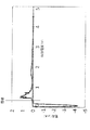
- the stored data may be read from the memory cell by comparing a voltage generated between the positive electrode and the negative electrode with a reference voltage.
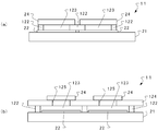
- the positive electrode (anode) 22 is formed of a metal such as Au, Pt, Ni, Cr, Co, Mn, Fe, or Mo, or an alloy thereof, a nitride thereof, or a conductor such as oxide thereof.
- the positive electrode 22 is formed on the insulating substrate 21 to a thickness of 50 to 500 nm, for example, about 100 nm.
- the material of the negative electrode 24 is not limited to Li. However, it is desirable that the material can contain a large amount of Li and has a low standard electrode potential (base material).
- the material of the negative electrode 24 is, for example, Li-based Li 4 Ti 5 O 2 , LiTi 2 O 4 , or at least one of C, In, Ag, Mg, Ca, Al, Si, Ge, Sn, Ga, Zn, Furthermore, an alloy of these and Li can be given as an example. That is, a material containing any of Li, C, In, Ag, Mg, Ca, Al, Si, Ge, Sn, Ga, and Zn can be used. Also, alloys of the above elements and Li can be used. Further, if the above conditions i) to iii) are satisfied, Li may not be contained.
- the application time of the first voltage applied to charge the memory cell 11 is necessary for decomposing most of the compound (preferably 80% or more) deposited on the positive electrode 22 in the discharged state. It is desirable that the time is longer than the time during which a current sufficient to supply a sufficient amount of charge flows.
- the storage circuit 101 includes a memory cell array 121, a row decoder 131, a column decoder 132, a read / write controller 133, and a write data controller 134.
- the output terminal of the AND gate RAj is connected to the gate of the read transistor RTj.
- a column line CLj is connected to one input terminal of the AND gate RAj, and a read enable signal RE is applied from the read / write controller 133 to the other input terminal.
- the array of the memory cells 11 and the semiconductor substrate 41 are joined. Subsequently, the wiring pattern on the insulating substrate 21 and the circuit pattern on the semiconductor substrate 41 are connected.
Landscapes
- Semiconductor Memories (AREA)
Abstract
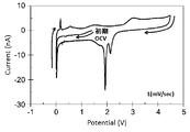
La présente invention concerne un accumulateur (11) qui est constitué d'une électrode positive (22), d'une couche d'électrolyte qui est formée sur l'électrode positive (22), et d'une électrode négative (24) qui est formée sur la couche d'électrolyte. La couche d'électrolyte contient, par exemple, une substance qui produit un composé par réaction avec l'électrode positive (22). La couche d'électrolyte contient, par exemple, une substance qui est la même qu'une substance contenue dans l'électrode négative (24), et qui produit un composé par réaction avec l'électrode positive (22). En ce qui concerne cet accumulateur (11), par exemple, un composé est décomposé par la circulation d'un courant de l'électrode positive (22) vers l'électrode négative (24) à travers la couche d'électrolyte, et un composé est produit par la circulation d'un courant de l'électrode négative (24) vers l'électrode positive (22) à travers la couche d'électrolyte.
Applications Claiming Priority (2)
| Application Number | Priority Date | Filing Date | Title |
|---|---|---|---|
| JP2015100906 | 2015-05-18 | ||
| JP2015-100906 | 2015-05-18 |
Publications (1)
| Publication Number | Publication Date |
|---|---|
| WO2016186148A1 true WO2016186148A1 (fr) | 2016-11-24 |
Family
ID=57320365
Family Applications (1)
| Application Number | Title | Priority Date | Filing Date |
|---|---|---|---|
| PCT/JP2016/064798 Ceased WO2016186148A1 (fr) | 2015-05-18 | 2016-05-18 | Accumulateur, circuit de stockage et procédé de stockage |
Country Status (1)
| Country | Link |
|---|---|
| WO (1) | WO2016186148A1 (fr) |
Citations (4)
| Publication number | Priority date | Publication date | Assignee | Title |
|---|---|---|---|---|
| JP2003060090A (ja) * | 2001-08-10 | 2003-02-28 | Matsushita Electric Ind Co Ltd | 不揮発性半導体記憶装置、その駆動方法及び製造方法 |
| JP2003157672A (ja) * | 2001-11-21 | 2003-05-30 | Tdk Corp | 情報記録素子 |
| JP2006303343A (ja) * | 2005-04-25 | 2006-11-02 | Matsushita Electric Ind Co Ltd | 半導体メモリとその動作方法 |
| JP2009043757A (ja) * | 2007-08-06 | 2009-02-26 | Sony Corp | 記憶素子および記憶装置 |
-
2016
- 2016-05-18 WO PCT/JP2016/064798 patent/WO2016186148A1/fr not_active Ceased
Patent Citations (4)
| Publication number | Priority date | Publication date | Assignee | Title |
|---|---|---|---|---|
| JP2003060090A (ja) * | 2001-08-10 | 2003-02-28 | Matsushita Electric Ind Co Ltd | 不揮発性半導体記憶装置、その駆動方法及び製造方法 |
| JP2003157672A (ja) * | 2001-11-21 | 2003-05-30 | Tdk Corp | 情報記録素子 |
| JP2006303343A (ja) * | 2005-04-25 | 2006-11-02 | Matsushita Electric Ind Co Ltd | 半導体メモリとその動作方法 |
| JP2009043757A (ja) * | 2007-08-06 | 2009-02-26 | Sony Corp | 記憶素子および記憶装置 |
Similar Documents
| Publication | Publication Date | Title |
|---|---|---|
| JP5197402B2 (ja) | 抵抗変化型記憶装置 | |
| US8295074B2 (en) | Memory cell | |
| CN100538878C (zh) | 可编程导体随机存取存储器以及向其中写入的方法 | |
| JP4475098B2 (ja) | 記憶素子及びその駆動方法 | |
| US8059446B2 (en) | Integrated circuit with memory having a current limiting switch | |
| US7239542B2 (en) | Storage apparatus | |
| CN113257300B (zh) | 基于铁电电容的存储装置 | |
| JP5736196B2 (ja) | 半導体装置 | |
| JP2006048298A (ja) | 演算回路 | |
| JP2005216387A (ja) | 記憶装置 | |
| CN103165172B (zh) | 混合存储器件及其控制方法、制备方法 | |
| US10255953B2 (en) | Bi-directional RRAM decoder-driver | |
| US8421048B2 (en) | Non-volatile memory with active ionic interface region | |
| US7583525B2 (en) | Method of driving storage device | |
| CN102568565A (zh) | 存储装置 | |
| TW201423744A (zh) | 電阻性切換記憶體 | |
| CN102592656A (zh) | 存储装置和其操作方法 | |
| JP2006032867A (ja) | 記憶素子及びその駆動方法 | |
| JP4625038B2 (ja) | メモリセル、メモリセルを備えたメモリ、およびメモリセル内にデータを書き込む方法 | |
| US20060154467A1 (en) | Method for the production of a memory cell, memory cell and memory cell arrangement | |
| WO2016186148A1 (fr) | Accumulateur, circuit de stockage et procédé de stockage | |
| US11929121B2 (en) | Storing one data value by programming a first memory cell and a second memory cell | |
| Pan | Experimental and simulation study of resistive switches for memory applications | |
| Walczyk et al. | Resistive switching and current status of HfO2-based RRAM | |
| JP2015005679A (ja) | スイッチング素子およびスイッチング素子のプログラム方法 |
Legal Events
| Date | Code | Title | Description |
|---|---|---|---|
| 121 | Ep: the epo has been informed by wipo that ep was designated in this application |
Ref document number: 16796541 Country of ref document: EP Kind code of ref document: A1 |
|
| NENP | Non-entry into the national phase |
Ref country code: DE |
|
| 122 | Ep: pct application non-entry in european phase |
Ref document number: 16796541 Country of ref document: EP Kind code of ref document: A1 |
|
| NENP | Non-entry into the national phase |
Ref country code: JP |