WO2016190422A1 - 太陽電池素子およびその製造方法 - Google Patents
太陽電池素子およびその製造方法 Download PDFInfo
- Publication number
- WO2016190422A1 WO2016190422A1 PCT/JP2016/065772 JP2016065772W WO2016190422A1 WO 2016190422 A1 WO2016190422 A1 WO 2016190422A1 JP 2016065772 W JP2016065772 W JP 2016065772W WO 2016190422 A1 WO2016190422 A1 WO 2016190422A1
- Authority
- WO
- WIPO (PCT)
- Prior art keywords
- layer
- solar cell
- cell element
- substrate
- polysiloxane
- Prior art date
- Legal status (The legal status is an assumption and is not a legal conclusion. Google has not performed a legal analysis and makes no representation as to the accuracy of the status listed.)
- Ceased
Links
Images


Classifications
-
- H—ELECTRICITY
- H10—SEMICONDUCTOR DEVICES; ELECTRIC SOLID-STATE DEVICES NOT OTHERWISE PROVIDED FOR
- H10F—INORGANIC SEMICONDUCTOR DEVICES SENSITIVE TO INFRARED RADIATION, LIGHT, ELECTROMAGNETIC RADIATION OF SHORTER WAVELENGTH OR CORPUSCULAR RADIATION
- H10F77/00—Constructional details of devices covered by this subclass
- H10F77/30—Coatings
- H10F77/306—Coatings for devices having potential barriers
- H10F77/311—Coatings for devices having potential barriers for photovoltaic cells
-
- H—ELECTRICITY
- H10—SEMICONDUCTOR DEVICES; ELECTRIC SOLID-STATE DEVICES NOT OTHERWISE PROVIDED FOR
- H10F—INORGANIC SEMICONDUCTOR DEVICES SENSITIVE TO INFRARED RADIATION, LIGHT, ELECTROMAGNETIC RADIATION OF SHORTER WAVELENGTH OR CORPUSCULAR RADIATION
- H10F10/00—Individual photovoltaic cells, e.g. solar cells
- H10F10/10—Individual photovoltaic cells, e.g. solar cells having potential barriers
- H10F10/14—Photovoltaic cells having only PN homojunction potential barriers
-
- H—ELECTRICITY
- H10—SEMICONDUCTOR DEVICES; ELECTRIC SOLID-STATE DEVICES NOT OTHERWISE PROVIDED FOR
- H10F—INORGANIC SEMICONDUCTOR DEVICES SENSITIVE TO INFRARED RADIATION, LIGHT, ELECTROMAGNETIC RADIATION OF SHORTER WAVELENGTH OR CORPUSCULAR RADIATION
- H10F71/00—Manufacture or treatment of devices covered by this subclass
- H10F71/129—Passivating
-
- H—ELECTRICITY
- H10—SEMICONDUCTOR DEVICES; ELECTRIC SOLID-STATE DEVICES NOT OTHERWISE PROVIDED FOR
- H10F—INORGANIC SEMICONDUCTOR DEVICES SENSITIVE TO INFRARED RADIATION, LIGHT, ELECTROMAGNETIC RADIATION OF SHORTER WAVELENGTH OR CORPUSCULAR RADIATION
- H10F77/00—Constructional details of devices covered by this subclass
- H10F77/30—Coatings
- H10F77/306—Coatings for devices having potential barriers
- H10F77/311—Coatings for devices having potential barriers for photovoltaic cells
- H10F77/315—Coatings for devices having potential barriers for photovoltaic cells the coatings being antireflective or having enhancing optical properties
-
- H—ELECTRICITY
- H10—SEMICONDUCTOR DEVICES; ELECTRIC SOLID-STATE DEVICES NOT OTHERWISE PROVIDED FOR
- H10F—INORGANIC SEMICONDUCTOR DEVICES SENSITIVE TO INFRARED RADIATION, LIGHT, ELECTROMAGNETIC RADIATION OF SHORTER WAVELENGTH OR CORPUSCULAR RADIATION
- H10F77/00—Constructional details of devices covered by this subclass
- H10F77/70—Surface textures, e.g. pyramid structures
- H10F77/703—Surface textures, e.g. pyramid structures of the semiconductor bodies, e.g. textured active layers
-
- H—ELECTRICITY
- H10—SEMICONDUCTOR DEVICES; ELECTRIC SOLID-STATE DEVICES NOT OTHERWISE PROVIDED FOR
- H10F—INORGANIC SEMICONDUCTOR DEVICES SENSITIVE TO INFRARED RADIATION, LIGHT, ELECTROMAGNETIC RADIATION OF SHORTER WAVELENGTH OR CORPUSCULAR RADIATION
- H10F10/00—Individual photovoltaic cells, e.g. solar cells
- H10F10/10—Individual photovoltaic cells, e.g. solar cells having potential barriers
- H10F10/14—Photovoltaic cells having only PN homojunction potential barriers
- H10F10/146—Back-junction photovoltaic cells, e.g. having interdigitated base-emitter regions on the back side
-
- H—ELECTRICITY
- H10—SEMICONDUCTOR DEVICES; ELECTRIC SOLID-STATE DEVICES NOT OTHERWISE PROVIDED FOR
- H10F—INORGANIC SEMICONDUCTOR DEVICES SENSITIVE TO INFRARED RADIATION, LIGHT, ELECTROMAGNETIC RADIATION OF SHORTER WAVELENGTH OR CORPUSCULAR RADIATION
- H10F77/00—Constructional details of devices covered by this subclass
- H10F77/20—Electrodes
- H10F77/206—Electrodes for devices having potential barriers
- H10F77/211—Electrodes for devices having potential barriers for photovoltaic cells
-
- Y—GENERAL TAGGING OF NEW TECHNOLOGICAL DEVELOPMENTS; GENERAL TAGGING OF CROSS-SECTIONAL TECHNOLOGIES SPANNING OVER SEVERAL SECTIONS OF THE IPC; TECHNICAL SUBJECTS COVERED BY FORMER USPC CROSS-REFERENCE ART COLLECTIONS [XRACs] AND DIGESTS
- Y02—TECHNOLOGIES OR APPLICATIONS FOR MITIGATION OR ADAPTATION AGAINST CLIMATE CHANGE
- Y02E—REDUCTION OF GREENHOUSE GAS [GHG] EMISSIONS, RELATED TO ENERGY GENERATION, TRANSMISSION OR DISTRIBUTION
- Y02E10/00—Energy generation through renewable energy sources
- Y02E10/50—Photovoltaic [PV] energy
- Y02E10/547—Monocrystalline silicon PV cells
-
- Y—GENERAL TAGGING OF NEW TECHNOLOGICAL DEVELOPMENTS; GENERAL TAGGING OF CROSS-SECTIONAL TECHNOLOGIES SPANNING OVER SEVERAL SECTIONS OF THE IPC; TECHNICAL SUBJECTS COVERED BY FORMER USPC CROSS-REFERENCE ART COLLECTIONS [XRACs] AND DIGESTS
- Y02—TECHNOLOGIES OR APPLICATIONS FOR MITIGATION OR ADAPTATION AGAINST CLIMATE CHANGE
- Y02P—CLIMATE CHANGE MITIGATION TECHNOLOGIES IN THE PRODUCTION OR PROCESSING OF GOODS
- Y02P70/00—Climate change mitigation technologies in the production process for final industrial or consumer products
- Y02P70/50—Manufacturing or production processes characterised by the final manufactured product
Definitions
- the present invention relates to a solar cell element (solar cell) and a manufacturing method thereof.
- a semiconductor substrate made of silicon is used as a photoelectric conversion material.
- a passivation layer is provided on the surface of the semiconductor substrate.
- This passivation layer is made of, for example, aluminum oxide.
- Aluminum oxide is easily altered by moisture penetration.
- a protective layer made of oxide or nitride is formed on the passivation layer by PECVD (Plasma Enhanced Chemical Vapor (Deposition) or the like (for example, JP2012-253356A and International Publication No. (See 2011/033826).
- One aspect of the solar cell element includes a semiconductor substrate having a p-type semiconductor region on one surface, a passivation layer containing aluminum oxide located on the p-type semiconductor region, and a position on the passivation layer. And a protective layer containing a polysiloxane layer having an alkyl group.
- One aspect of a method for manufacturing a solar cell element includes a step of forming a passivation layer containing aluminum oxide on the p-type semiconductor region of a semiconductor substrate having a p-type semiconductor region on one surface; And a step of forming a coating film containing a polysiloxane oligomer and a step of drying the coating film to form a protective layer containing a polysiloxane layer having an alkyl group.
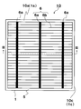
- FIG. 1 is a plan view showing the external appearance of the first surface side of the solar cell element.
- FIG. 2 is a plan view showing the appearance of the second surface side of the solar cell element.
- FIG. 3 is a cross-sectional view showing a cross section taken along line III-III in FIG.
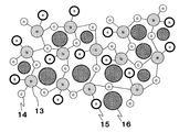
- FIG. 4 is a structural diagram showing the structure of the polysiloxane layer.
- 5 (a) to 5 (f) are cross-sectional views showing an example of steps of a method for manufacturing a solar cell element.
- 6 (g) to 6 (i) are cross-sectional views showing an example of steps of a method for manufacturing a solar cell element.
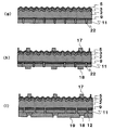
- FIGS. 7A to 7C are cross-sectional views showing examples of the portion A in FIG.
- FIG. 8 is a cross-sectional view showing another example of part A in FIG.
- the passivation layer may be deteriorated due to the influence of heat and plasma.
- the function of the passivation layer is lowered, and the photoelectric conversion efficiency of the solar cell element can be lowered. For this reason, the solar cell element which can maintain photoelectric conversion efficiency at high efficiency, and its manufacturing method are calculated
- FIGS. A solar cell element 10 is shown in FIGS.
- the solar cell element 10 includes a first surface 10a that is a light receiving surface on which light is mainly incident, and a second surface 10b that is a surface (back surface) located on the opposite side of the first surface 10a. And a side surface 10c.
- the solar cell element 10 includes a silicon substrate (hereinafter referred to as a substrate) 1 as a semiconductor substrate.
- the substrate 1 also has a first surface 1a, a second surface 1b located on the opposite side of the first surface 1a, and a side surface 1c.
- the substrate 1 is a first semiconductor layer 2 that is a one-conductivity type (for example, p-type) semiconductor region, and a reverse conductivity type (for example, n-type) semiconductor region that is provided on the first surface 10a side of the first semiconductor layer 2.
- a second semiconductor layer 3 Further, the solar cell element 10 includes a BSF (Back Surface Field) layer 4, an antireflection layer 5, a first electrode 6, a second electrode 7, a third electrode 8, a passivation layer 9 and a protective layer 11.
- BSF Back Surface Field
- the substrate 1 is, for example, a single crystal or polycrystalline silicon substrate, and includes a first semiconductor layer 2 and a second semiconductor layer 3 provided on the first surface 1 a side of the first semiconductor layer 2. . Since the substrate 1 may be a semiconductor substrate having the first semiconductor layer 2 and the second semiconductor layer 3, the substrate 1 may be a semiconductor substrate such as germanium, selenium, or gallium arsenide.
- the substrate 1 is, for example, a p-type silicon substrate.
- the thickness is, for example, about 100 to 250 ⁇ m.
- substrate 1 is not specifically limited, When manufacturing a solar cell module from the solar cell element 10, if the substantially square shape is planar view, the clearance gap between elements may be made small.
- an impurity such as boron or gallium is contained as a dopant.
- the second semiconductor layer 3 is stacked on the first semiconductor layer 2. As a result, the second semiconductor layer 3 has a pn junction formed at the interface with the first semiconductor layer 2.
- the second semiconductor layer 3 is a semiconductor layer having a conductivity type opposite to that of the first semiconductor layer 2 (n-type in this embodiment), and is provided on the first surface 1 a side of the first semiconductor layer 2.
- the first semiconductor layer 2 is a p-type conductive substrate 1
- the second semiconductor layer 3 can be formed by diffusing an impurity such as phosphorus as a dopant on the first surface 1a side.
- a fine uneven structure (texture) for reducing the reflectance of the irradiated light may be provided on the first surface 1a side of the substrate 1.
- the height of the convex portions of the texture is about 0.1 to 10 ⁇ m, and the interval between adjacent convex portions is about 0.1 to 20 ⁇ m.
- the concave portion may have a substantially spherical shape, or the convex portion may have a pyramid shape.
- the above-mentioned “height of the convex portion” is, for example, a straight line passing through the bottom surface of the concave portion in FIG. 3 as a reference line, and from the reference line to the top surface of the convex portion in a direction perpendicular to the reference line. It is distance.
- the “interval between convex portions” is a distance between the centers of the top surfaces of adjacent convex portions in a direction parallel to the reference line.
- the antireflection layer 5 has a function of reducing the reflectance of light irradiated on the first surface 10 a of the solar cell element 10.
- the antireflection layer 5 is made of, for example, a silicon oxide, aluminum oxide, or silicon nitride layer.
- the refractive index and thickness of the antireflection layer 5 may be appropriately selected from refractive indexes and thicknesses capable of realizing low reflection conditions for light in a wavelength range that can be absorbed by the substrate 1 and contribute to power generation in sunlight. Good.
- the antireflective layer 5 can have a refractive index of about 1.8 to 2.5 and a thickness of about 20 to 120 nm.
- the BSF layer 4 is located on the second surface 1b side of the substrate 1 and may have the same conductivity type as the first semiconductor layer 2 (p-type in this embodiment).
- the concentration of the dopant contained in the BSF layer 4 is higher than the concentration of the dopant contained in the first semiconductor layer 2.
- the dopant is present at a concentration higher than the concentration of the dopant doped to make the first semiconductor layer 2 have one conductivity type.
- the BSF layer 4 forms an internal electric field on the second surface 1 b side of the substrate 1. This makes it difficult for minority carrier recombination to occur near the surface of the second surface 1b of the substrate 1 so that the photoelectric conversion efficiency does not decrease.
- the BSF layer 4 can be formed, for example, by diffusing a dopant such as boron or aluminum on the second surface 1b side of the substrate 1.
- concentration of the dopant contained in the first semiconductor layer 2 and the BSF layer 4 may be about 5 ⁇ 10 15 to 1 ⁇ 10 17 atoms / cm 3 and 1 ⁇ 10 18 to 5 ⁇ 10 21 atoms / cm 3 , respectively. it can.
- the BSF layer 4 is preferably present at the contact portion between the third electrode 8 and the substrate 1 described later.
- the first electrode 6 is an electrode provided on the first surface 1 a side of the substrate 1. As shown in FIG. 1, the first electrode 6 includes a first output extraction electrode 6a and a plurality of linear first current collecting electrodes 6b.
- the first output extraction electrode 6a is an electrode for extracting electricity obtained by power generation to the outside.
- the length in the short direction (hereinafter referred to as width) is about 0.5 to 2.5 mm.
- At least a part of the first output extraction electrode 6a intersects the first current collecting electrode 6b and is electrically connected.
- the first collector electrode 6 b is an electrode for collecting electricity generated from the substrate 1.
- the first current collecting electrode 6b has a plurality of linear shapes, and the width thereof is, for example, about 50 to 200 ⁇ m.
- the width of the first collector electrode 6b is smaller than the width of the first output extraction electrode 6a.
- a plurality of first current collecting electrodes 6b are provided with an interval of about 1 to 3 mm.
- the thickness of the first electrode 6 is about 10 to 40 ⁇ m.
- Such a first electrode 6 can be formed, for example, by applying a first metal paste containing silver as a main component into a desired shape by screen printing or the like and then baking it.
- a main component shows that the containing mass with respect to the whole component is 50 mass% or more.
- the second electrode 7 and the third electrode 8 are electrodes provided on the second surface 1b side of the substrate 1 as shown in FIGS.
- the second electrode 7 is an electrode for taking out the electricity obtained by the power generation by the solar cell element 10 to the outside.
- the second electrode 7 is formed on the substrate 1 through the passivation layer 9 or the protective layer 11 or through the passivation layer 9 and the protective layer 11.
- the shape of the second electrode 7 may be linearly arranged in a dot shape (or island shape), or may be a strip shape (or a line shape).
- the second electrode 7 has a thickness of about 10 to 30 ⁇ m and a width of about 1.3 to 7 mm.
- the second electrode 7 contains silver as a main component.
- Such a second electrode 7 can be formed, for example, by applying a metal paste containing silver as a main component into a desired shape by screen printing or the like and then baking it.
- the third electrode 8 is an electrode for collecting electricity generated from the substrate 1 on the second surface 1 b of the substrate 1, and is electrically connected to the second electrode 7. It is provided as follows. At this time, at least a part of the second electrode 7 may be connected to the third electrode 8. Further, a part of the third electrode 8 is connected to the first semiconductor layer 2 of the substrate 1 by filling the inside of a large number of holes 22 penetrating the passivation layer 9 and the protective layer 11. The third electrode 8 is formed so as to cover substantially the entire surface of the protective layer 11 except for the outer peripheral portion of about 0.3 to 2 mm from the end portion of the substrate 1.
- the third electrode 8 includes aluminum as a main component. The thickness of the third electrode 8 is about 15 to 50 ⁇ m.
- the third electrode 8 can be formed by applying a metal paste containing aluminum as a main component into a desired shape and baking it.
- the passivation layer 9 is formed on at least the first semiconductor layer 2 which is the p-type semiconductor region of the substrate 1 and has a function of reducing minority carrier recombination.
- the passivation layer 9 for example, a film containing aluminum oxide formed by an ALD (Atomic Layer Deposition) method or the like is preferably used.
- the thickness of the passivation layer 9 is about 10 to 200 nm.
- the protective layer 11 is located on the passivation layer 9 containing aluminum oxide. Thereby, it can be set as the solar cell element 1 excellent in reliability, such as moisture resistance. Further, the protective layer 11 includes a polysiloxane layer having an alkyl group having a molecular weight of about 5 to 10 ⁇ 10 5 , for example. In the polysiloxane layer having an alkyl group, an alkyl group such as a methyl group (CH 3 ) or an ethyl group (C 2 H 5 ) is bonded to a structure having many Si—O—Si siloxane bonds.
- the protective layer 11 including a polysiloxane layer having an alkyl group can be formed by applying a polysiloxane oligomer on the passivation layer 9 and then drying and curing.
- the surface of the polysiloxane layer has a structure with little polarization charge. Thereby, since the protective layer 11 has water repellency, it becomes difficult for water molecules to pass through the protective layer 11.
- the thickness of the protective layer 11 is about 0.1 to 10 ⁇ m (or 1 to 5 ⁇ m)
- the solar cell element 10 having excellent reliability such as moisture resistance can be obtained.
- the protective layer 11 includes a polysiloxane layer having an alkyl group, for example, time-of-flight secondary ion mass spectrometry (TOF-SIMS), time-of-flight, secondary, ion-mass, spectrometry, or Fourier transform infrared spectroscopy (FT- IR; Fourier Transform Infrared Spectroscopy).
- TOF-SIMS time-of-flight secondary ion mass spectrometry
- FT- IR Fourier transform infrared spectroscopy
- silica particles 16 having a plurality of silicon atoms are preferably dispersed in a polysiloxane layer having an alkyl group (hereinafter simply referred to as a polysiloxane layer).
- the polysiloxane layer has a three-dimensional structure composed of silicon atoms 13, oxygen atoms 14, and alkyl groups 15.
- the silica particle 16 which has several silicon atoms like colloidal silica exists in the area
- the average particle diameter of the silica particles 16 may be about 20 to 200 nm.
- the polysiloxane layer has the silica particles 16 having a plurality of silicon atoms, the moisture permeability of the protective layer 11 can be further reduced, and the reliability of the solar cell element 10 can be further improved. Further, the dispersion of the silica particles 16 having a plurality of silicon atoms in the polysiloxane layer can be determined by, for example, TOF-SIMS.
- the protective layer 11 may include at least one of a carboxyl group (COOH) and a carbonate group (CO 3 ) in the polysiloxane layer. Oxidation of part of the alkyl group in the polysiloxane layer generates at least one of a carboxyl group and a carbonate group.
- the polysiloxane layer since the polysiloxane layer forms a ⁇ electron covalent bond, it exhibits a negative fixed charge similarly to the passivation layer 9 containing aluminum oxide. Thereby, the passivation effect of the passivation layer 9 can be further improved, and the photoelectric conversion efficiency of the solar cell element 10 can be further improved.
- the polysiloxane layer containing at least one of a carboxyl group and a carbonate group can be formed as follows.
- a polysiloxane oligomer solution having an alkyl group is applied to the substrate 1.
- the coated substrate 1 is dried and cured at about 100 to 300 ° C. for about 30 seconds to 20 minutes.
- a temperature of about 700 to 900 ° C. for about 0.1 to several tens of seconds a part of the alkyl groups in the film is oxidized.
- a polysiloxane layer can be formed on the substrate 1.
- the fact that the polysiloxane layer contains a carboxyl group or a carbonate group can be determined by XPS (X-ray Photoelectron Spectroscopy) or the like.
- the substrate 1 may be single crystal silicon or polycrystalline silicon.
- the substrate 1 is formed by, for example, an existing CZ (Czochralski) method or a casting method.
- CZ Czochralski
- a p-type polycrystalline silicon substrate is used as the substrate 1
- a polycrystalline silicon ingot is produced by a casting method.
- the dopant for example, boron may be added so that the specific resistance of the ingot is about 1 to 5 ⁇ ⁇ cm.
- the substrate is manufactured by slicing the ingot into a square shape having a side of about 150 to 160 mm square and a thickness of about 100 to 200 ⁇ m.
- the surface of the substrate 1 may be subjected to a very small amount of etching with an aqueous solution such as NaOH, KOH, hydrofluoric acid, or hydrofluoric acid.
- an aqueous solution such as NaOH, KOH, hydrofluoric acid, or hydrofluoric acid.
- a texture may be formed on the first surface 1a of the substrate 1 in order to reduce reflection of light on the surface.
- a texture formation method a wet etching method using an alkaline solution such as NaOH or an acid solution such as hydrofluoric acid, or a dry etching method using RIE (Reactive Ion Etching) or the like can be used.
- an n-type second semiconductor layer 3 is formed on the first surface 1a of the substrate 1 having a texture.
- the second semiconductor layer 3 is formed by applying a coating thermal diffusion method in which paste-like phosphorous pentoxide (P 2 O 5 ) is applied to the surface of the substrate 1 for thermal diffusion, and gaseous phosphorus oxychloride (POCl 3 ) is used. It is formed by a vapor phase thermal diffusion method using a diffusion source.
- the second semiconductor layer 3 is formed to have a thickness of about 0.1 to 2 ⁇ m and a sheet resistance value of about 40 to 200 ⁇ / ⁇ .
- the substrate 1 is heat-treated for about 5 to 30 minutes at a temperature of about 600 to 800 ° C. in an atmosphere having a diffusion gas composed of POCl 3 or the like, so that phosphosilicate glass (PSG) is formed on the substrate. 1 formed on the surface. Thereafter, the substrate 1 is heat-treated for about 10 to 40 minutes at a high temperature of about 800 to 900 ° C. in an inert gas atmosphere such as argon or nitrogen. As a result, phosphorus diffuses from the PSG to the substrate 1, and the second semiconductor layer 3 is formed on the first surface 1 a side of the substrate 1.
- PSG phosphosilicate glass
- the second semiconductor layer 3 formed on the second surface 1b side is removed by etching. To do. Thereby, the p-type first semiconductor layer 2 is exposed on the second surface 1b side.
- the second semiconductor layer 3 formed on the second surface 1b side is removed by immersing only the second surface 1b side of the substrate 1 in the hydrofluoric acid nitric acid mixed solution. Thereafter, PSG adhering to the first surface 1a side of the substrate 1 when the second semiconductor layer 3 is formed is removed by etching with hydrofluoric acid. At this time, the second semiconductor layer 3 formed on the side surface 1c of the substrate 1 may also be removed.
- the polycrystalline substrate 1 in which the second semiconductor layer 3 as the n-type semiconductor layer is located on the first surface 1a side and the texture is formed on the surface can be prepared.
- the passivation layer 9 is formed. As shown in FIG. 5D, a passivation layer 9 made of aluminum oxide is formed on the second surface 1 b of the first semiconductor layer 2.
- a method for forming the passivation layer 9 for example, an ALD method, a PECVD method, or the like can be used.
- the ALD method may be excellent in covering the surface of the substrate 1. For this reason, the passivation layer 9 produced by the ALD method can further increase the passivation effect.
- the substrate 1 on which the second semiconductor layer 3 is formed is placed in the chamber of the film forming apparatus. Then, the following steps A to D are repeated a plurality of times while the substrate 1 is heated in a temperature range of 100 ° C. to 250 ° C. Thus, a passivation layer 9 made of aluminum oxide and having a desired thickness is formed on the substrate 1.
- the contents of steps A to D are as follows.
- Step A An aluminum material such as trimethylaluminum (TMA) for forming aluminum oxide is supplied onto the substrate 1 together with a carrier gas such as argon (Ar) gas or nitrogen gas. As a result, the aluminum raw material is adsorbed on the entire periphery of the substrate 1.
- the time for supplying TMA may be about 15 to 3000 milliseconds, for example.
- the surface of the substrate 1 is preferably terminated with an OH group.
- the surface of the substrate 1 has a Si—O—H structure, a covalent bond is easily formed at the interface between the surface of the substrate 1 and the formed aluminum oxide film. Thereby, the joint strength between the surface of the substrate 1 and the aluminum oxide film can be improved, and the reliability of the solar cell element 10 can be further improved.
- This Si—O—H structure can be formed, for example, by treating the substrate 1 with dilute hydrofluoric acid and then washing with pure water.
- Step B The inside of the chamber of the film forming apparatus is cleaned with nitrogen gas, and the aluminum material in the chamber is removed. Furthermore, aluminum materials other than the components chemically adsorbed at the atomic layer level among the aluminum materials physically and chemically adsorbed on the substrate 1 are removed.
- the time required for purifying the inside of the chamber with nitrogen gas may be, for example, about 1 to several tens of seconds.
- Step C By supplying an oxidizing agent such as water or ozone gas into the chamber of the film forming apparatus, the alkyl group contained in the TMA is removed and replaced with an OH group. As a result, an atomic layer of aluminum oxide is formed on the substrate 1. Note that the time during which the oxidizing agent is supplied into the chamber is preferably about 500 to 1500 milliseconds. Further, by supplying H together with the oxidizing agent into the chamber, hydrogen atoms are more easily contained in the formed aluminum oxide film.
- an oxidizing agent such as water or ozone gas
- Step D The inside of the chamber of the film forming apparatus is cleaned with nitrogen gas, and the oxidizing agent in the chamber is removed. At this time, for example, the oxidizing agent that has not contributed to the reaction during the formation of atomic layer level aluminum oxide on the substrate 1 is removed. Note that the time for purging the inside of the chamber with nitrogen gas may be about 1 to several tens of seconds, for example.
- an aluminum oxide film having a desired film thickness (for example, about 10 to 200 nm) is formed by repeating a series of steps A to D a plurality of times.
- the aluminum oxide is formed using TMA as the aluminum material
- other materials may be used as the aluminum material.
- the aluminum raw material for example, triethylaluminum (TEA) can be used.
- TSA triethylaluminum
- the material that can be supplied in a gaseous state may be supplied after being diluted with nitrogen gas, carbon dioxide gas or the like as a carrier gas.
- the passivation layer 9 can be easily formed around the entire periphery of the substrate 1 including the side surface 1c of the substrate 1 by using the ALD method. In this case, only the first surface 1a and the side surface 1c of the substrate 1 are immersed in hydrofluoric acid or the like. Alternatively, after applying an acid resistant resist to the passivation layer 9 on the second surface 1b, etching or the like is performed with hydrofluoric acid or the like. In this way, unnecessary passivation layer 9 may be removed.
- an antireflection layer 5 made of a silicon nitride film is formed on the first surface 1 a side of the substrate 1.
- the antireflection layer 5 is formed using, for example, PECVD or sputtering. If the PECVD method is used, the substrate 1 is heated in advance at a temperature higher than the temperature during film formation. Thereafter, a mixed gas of silane (SiH 4 ) and ammonia (NH 3 ) is diluted with nitrogen (N 2 ), the reaction pressure is set to about 50 to 200 Pa, plasma is formed by glow discharge decomposition, and the heated substrate 1 is heated. A silicon nitride film is deposited. Thereby, the antireflection layer 5 is formed on the substrate 1.
- the film forming temperature at this time is about 350 to 650 ° C. Further, a frequency of 10 to 500 kHz is used as the frequency of the high frequency power source necessary for glow discharge.
- the gas flow rate is appropriately determined depending on the size of the reaction chamber. For example, the gas flow rate may be in the range of 150 to 6000 ml / min (sccm), and the flow rate ratio B / A between the silane flow rate A and the ammonia flow rate B may be 0.5 to 15.
- the protective layer 11 is formed. As shown in FIG. 5 (f), the protective layer 11 is formed on the passivation layer 9.
- the protective layer 11 is formed as follows. First, a silicon compound represented by the general formula R n SiX (4-n) (R is an alkyl group, X is an alkoxy group, and n is an integer from 0 to 3) is used as a material.
- the alkyl group R may have about 1 to 20 carbon atoms.
- the alkoxy group X is, for example, a methoxy group, an ethoxy group, a propoxy group, or the like.
- Such silicon compounds are for example methyltribromosilane, methyltrimethoxysilane, methyltriethoxysilane, methyltriisopropoxysilane, ethyltribromosilane, ethyltrimethoxysilane, ethyltriethoxysilane or ethyltriisoporopropoxysilane. Etc. Next, this silicon compound material is hydrolyzed and then subjected to polycondensation to produce a polysiloxane oligomer having a molecular weight of about 2000 to 6000.
- the polysiloxane oligomer solution is applied to substantially the entire surface of the passivation layer 9 by using a spray, roller, die coater, roll coater or spin coater, screen printer, or the like. Thereafter, the coated substrate 1 is dried and cured at a temperature of about 100 to 300 ° C. for a time of about 30 seconds to 20 minutes. By these, the protective layer 11 including a polysiloxane layer can be formed.
- the passivation layer 9 does not receive plasma damage (etching damage and defect generation of the aluminum oxide film due to collision of electrons generated by the plasma, and impurity mixing into the aluminum oxide film) when the protective layer 11 is formed. . Furthermore, there is no deterioration of the passivation layer 9 due to the influence of heat, and the adhesion strength with the substrate 1 is unlikely to decrease.
- a silica dispersion is prepared by dispersing amorphous silica in an amount of about 5 to 30% by mass in water or a mixture of water and alcohol. Then, it can be formed by adding about 70 to 500% by mass of the above-mentioned silicon compound material to this silica dispersion.
- the hole 22 may be formed by laser beam irradiation, or may be formed by etching after forming a patterned etching mask.
- the hole 22 is provided in a circular shape or a linear shape in plan view.
- the connection conductor portion 12 is formed into a circular shape, the diameter is about 30 to 150 ⁇ m, and the connection conductor portion 12 is formed so as to be distributed almost uniformly at about 100 to 500 per 1 cm 2 .
- the first electrode 6 (first output extraction electrode 6a, first current collecting electrode 6b), the second electrode 7 and the third electrode 8 are formed as follows.
- the first paste 17 includes, for example, at least one of silver and copper as a main component of the conductive component.
- the conductive paste contains metal powder such as silver (for example, a particle size of about 0.05 to 20 ⁇ m, or about 0.1 to 5 ⁇ m) about 70 to 85% by mass of the total mass of the conductive paste.
- a kneaded glass frit and an organic vehicle is used as the conductive paste.
- the organic vehicle is obtained, for example, by adding a resin component used as a binder to an organic solvent.
- an acrylic resin or an alkyd resin can be used in addition to a cellulose resin such as ethyl cellulose.
- the organic solvent for example, diethylene glycol monobutyl ether acetate, terpineol or diethylene glycol monobutyl ether can be used.
- the organic vehicle may be contained in an amount of about 5 to 20% by mass of the total mass of the conductive paste.
- the glass frit component lead glass such as SiO 2 —Bi 2 O 3 —PbO, Al 2 O 3 —SiO 2 —PbO, or the like can be used as a glass material.
- non-lead glass such as B 2 O 3 —SiO 2 —Bi 2 O 3 or B 2 O 3 —SiO 2 —ZnO can also be used.
- the glass frit may be contained in an amount of about 2 to 15% by mass with respect to the total mass of the conductive paste.
- the second electrode 7 that is the second surface 10b side electrode is manufactured using a conductive paste (second paste 18) containing, as a main component, a metal powder made of only silver, an organic vehicle, glass frit, and the like.
- the component of the second paste 18 may be the same as that of the first paste 17.
- a method for applying the second paste 18 for example, a screen printing method or the like can be used. After this application, the solvent is evaporated and dried at a predetermined temperature.
- the third electrode 8 is formed using a third paste 19.
- the 3rd paste 19 uses what contains aluminum as a main component.
- the conductive paste contains aluminum powder (for example, a particle size of about 0.05 to 20 ⁇ m or about 0.1 to 5 ⁇ m) about 65 to 80% by mass of the total mass of the conductive paste, and glass frit and A kneaded organic vehicle is used.
- the organic vehicle is obtained, for example, by adding a resin component used as a binder to an organic solvent.
- the binder an acrylic resin or an alkyd resin is used in addition to a cellulose-based resin such as ethyl cellulose.
- the organic solvent for example, diethylene glycol monobutyl ether acetate, terpineol or diethylene glycol monobutyl ether is used.
- the organic vehicle may be contained in an amount of about 5 to 30% by mass of the total mass of the conductive paste.
- a lead-based glass such as a SiO 2 —Bi 2 O 3 —PbO system or an Al 2 O 3 —SiO 2 —PbO system can be used.
- non-lead glass such as B 2 O 3 —SiO 2 —Bi 2 O 3 or B 2 O 3 —SiO 2 —ZnO can be used.
- the glass frit may be contained in the conductive paste at about 2 to 15% by mass.
- the third paste 19 overlaps the outer periphery of the already applied second paste 18 and covers substantially the entire surface of the protective layer 11 except for the outer periphery of about 0.3 to 2 mm from the end of the substrate 1.
- As a coating method a screen printing method or the like can be used.
- the third paste 19 is also filled in the connection conductor portion 12. After this application, the solvent may be evaporated and dried at a predetermined temperature.
- the substrate 1 on which the first paste 17, the second paste 18 and the third paste 19 are applied has a maximum temperature of about 700 to 900 ° C. and a maximum temperature of about 0.1 seconds to several tens of seconds in a baking furnace. Maintain and fire. Thereby, each electrically conductive paste sinters and the 1st electrode 6, the 2nd electrode 7, and the 3rd electrode 8 are formed as shown in FIG. By this firing, the first paste 17 fires through the antireflection layer 5 and is connected to the n-type second semiconductor layer 3 on the first surface 1 a of the substrate 1, thereby forming the first electrode 6.
- the third paste 19 is also connected to the p-type first semiconductor layer 2 on the second surface 1 b at the end of the connection conductor portion 12, and the third electrode 8 is formed. Along with the formation of the third electrode 8, the BSF layer 4 is also formed. Further, the second paste 18 is also baked to form the second electrode 7. However, since the second paste 18 and the third paste 19 on the protective layer 11 are blocked by the protective layer 11, there is almost no influence on the passivation layer 9. Further, by using the protective layer 11 containing polysiloxane having an alkyl group, for example, even when the thickness of the protective layer 11 is as thin as 0.1 to 5 ⁇ m, damage to the passivation layer 9 due to baking of the conductive paste is caused. Can be reduced. In addition, by firing the conductive paste, the polysiloxane layer includes at least one of a carboxyl group and a carbonate group as described above. Thereby, it can be set as the highly efficient solar cell element 10 excellent in a weather resistance.
- the passivation layer 9 may be formed before the antireflection layer 5 is formed, and the passivation layer 9 may be provided on or below the antireflection layer 5.
- the firing in the electrode forming step is performed to form the third electrode 8 after firing the first paste and the second paste for forming the first electrode 6 and the second electrode 7 having similar components.
- the third paste may be fired separately.
- the protective layer 11 may further include a silica (SiO 2 ) layer.
- the protective layer 11 includes a polysiloxane layer and a silica layer.
- the protective layer 11 has a laminated structure having a silica layer on at least one of the first surface and the second surface (the surface opposite to the first surface) of the polysiloxane layer. In this case, even if pinholes or thin portions are formed in the polysiloxane layer, the silica layer can compensate for this portion. Thereby, the reliability of the solar cell element 10 can be improved. Further, the polysiloxane layer and the silica layer may be positioned side by side.
- the silica layer 20 of the protective layer 11 may be in contact with the passivation layer 9.
- the protective layer 11 includes a silica layer 20 located on the passivation layer 9 and a polysiloxane layer 21 located on the silica layer 20. May be.
- the silica layer 20 may be in contact with the passivation layer 9 on the first surface and may be in contact with the polysiloxane layer 21 on the second surface so that the polysiloxane layer 21 does not directly contact the passivation layer 9.
- the alteration of the passivation layer 9 (alteration from aluminum oxide to, for example, aluminum hydroxide) can be reduced due to the influence of moisture contained in the polysiloxane oligomer. For this reason, the photoelectric conversion efficiency of the solar cell element 10 can be improved.
- the silica layer 20 is formed by using, for example, an ALD method excellent in coverage.
- a raw material gas by the ALD method for example, a silicon raw material such as bisdiethylaminosilane (BDEAS) or N, N, N ′, N ′, tetraethylsilanediamine gas, and ozone (O 3 ) or water vapor is used. I can make a film.
- the film thickness of the silica layer 20 is preferably thinner than that of the passivation layer 9.
- the negative fixed charge of aluminum oxide forming the passivation layer 9 becomes more dominant than the positive fixed charge of the silica layer 20, so that the passivation effect of the passivation layer 9 is difficult to be lowered.
- the thickness of the silica layer 20 may be about 8 to 190 nm.
- the silica layers 20 and the polysiloxane layers 21 may be alternately arranged in a direction parallel to the main surface of the passivation layer 9.
- the silica layer 20 is thinner than the polysiloxane layer 21.
- the aluminum of the third electrode 8 is partly fired through the silica layer 20 and the passivation layer 9 and is easily connected to the first semiconductor layer 2.
- the number of the connection conductor parts 12 which penetrate the passivation layer 9 and the protective layer 11 can be reduced, or the formation itself of the connection conductor parts 12 can be omitted, and the man-hour of the manufacturing process can be reduced.
- the protective layer 11 shown in FIG. 7B can be formed by the following method, for example. After the silica layer 20 is formed on substantially the entire surface of the passivation layer 9, the silica layer 20 is partially removed by etching using a photolithography method or the like. Then, it is good to apply
- the protective layer 11 shown in FIG. 7C is obtained by providing a partially missing polysiloxane layer 21 on the silica layer 20.
- This can be formed, for example, by the following method.
- a silica layer 20 is formed on substantially the entire surface of the passivation layer 9.
- a partially missing polysiloxane layer 21 is provided on the silica layer 20 by screen printing.
- a polysiloxane oligomer is applied to a predetermined pattern by a screen printing method and dried and cured.
- the third electrode 8 is also formed in a portion where the polysiloxane layer 21 is partially missing.
- the third electrode 8 aluminum as a component of the third electrode 8 fires through the silica layer 20 and the passivation layer 9, and the third electrode 8 is partially connected to the first semiconductor layer 2. Is done. Thereby, the number of the connection conductor parts 12 which penetrate the passivation layer 9 and the protective layer 11 can be reduced, or the hole forming process can be omitted, and the man-hour of the manufacturing process can be reduced.
- a metal layer covering the protective layer 11 may be further provided, and the silica layer 20 of the protective layer 11 may be in contact with the metal layer.
- the metal layer is the third electrode 8 whose main component is aluminum, and the third electrode 8 is formed so as to cover substantially the entire surface of the protective layer 11 as described above.
- one surface of the silica layer 20 of the protective layer 11 may be in contact with the third electrode 8, and the other surface may be in contact with the polysiloxane layer 21.
- the silica layer 20 and the glass frit which is one of the components of the 3rd electrode 8 can be made to react by baking.
- the adhesive strength improves compared with the case where the metal layer has contact
- the solar cell element 10 of the example was manufactured as follows.
- a p-type polycrystalline silicon substrate doped with boron was prepared as the substrate 1.
- the substrate 1 was obtained by slicing a polycrystalline silicon ingot produced by a casting method.
- a substrate 1 having a square planar shape with a specific resistance value of about 1 ⁇ ⁇ cm, a thickness of about 200 ⁇ m, and a side of about 156 mm was prepared.
- the substrate 1 was etched to a depth of about 7 to 12 ⁇ m from the surface using an aqueous NaOH solution. Thereafter, a fine texture was formed on the first surface 1a side by RIE.
- an n-type region was formed on the entire surface of the substrate 1 by vapor phase thermal diffusion using phosphorus oxychloride as a diffusion source.
- This n-type region was formed so as to have a sheet resistance of about 60 to 100 ⁇ / ⁇ .
- substrate 1 were immersed in the hydrofluoric acid nitric acid mixed solution, and the n-type area
- a passivation layer 9 made of aluminum oxide was formed to a thickness of about 10 to 20 nm on the entire surface of the substrate 1 by ALD.
- the passivation layer 9 was formed by holding the substrate 1 in an upright state in the chamber of the ALD apparatus and maintaining the temperature of the substrate 1 at about 200 ° C. under reduced pressure.
- TMA was used as the source gas
- N 2 , He, and H 2 were used as the carrier gas and the purge gas.
- Ozone was used as the oxidizing gas.
- the passivation layer 9 was formed by repeating the above-described cycle from step A to step D a plurality of times using an ALD apparatus.
- the time required for each step per cycle from step A to step D was set to step A: about 4 seconds, step B: about 5 seconds, step C: about 1 second, and step D: about 5 seconds.
- the film-forming time (cycle number) was determined from the film-forming speed calculated beforehand.
- a reflection made of a silicon nitride film having a refractive index of 1.9 to 2.1 and a film thickness of about 70 to 90 nm is formed on the first surface 1a of the substrate 1 by PECVD.
- the prevention layer 5 was formed.
- the antireflection layer 5 was formed by setting the inside of the chamber to about 500 ° C., and making a gas obtained by diluting a mixed gas of silane and ammonia with nitrogen into plasma by glow discharge decomposition to deposit silicon nitride.
- a protective layer 11 was formed on the passivation layer 9.
- the protective layer 11 of the example was formed as follows. First, a silicon compound material having a structure of R n SiX (4-n) (R is a methyl group, X is a methoxy group, and n is an integer of 0 to 3) was prepared. Next, this silicon compound material was hydrolyzed and then subjected to polycondensation to produce a polysiloxane oligomer having a molecular weight of about 3000 to 5000.
- the polysiloxane oligomer solution was applied on substantially the entire surface of the passivation layer 9 by using a roll coater. Thereafter, the coated substrate 1 was dried at a temperature of about 250 ° C. for about 10 minutes. By these, the protective layer 11 including the polysiloxane layer having an alkyl group could be formed. The thickness of the protective layer 11 was about 3 to 5 ⁇ m.
- connection conductor portion 12 was formed.
- the connecting conductor portion 12 was formed by laser beam irradiation using a second harmonic laser device of an Nd: YAG laser.
- the connection conductor portions 12 were provided in a circular shape having a diameter of about 90 to 110 ⁇ m in plan view, and were formed so as to be uniformly distributed about 300 pieces per 1 cm 2 .
- the first paste 17 was applied on the first surface 1 a of the substrate 1 using a screen printing method.
- the 1st paste 17 used what has silver as a main component.
- silver metal powder (mixed with a particle size of about 0.1 to 5 ⁇ m) is contained in an amount of about 87% by mass of the total mass of the conductive paste.
- the organic vehicle used ethyl cellulose as the binder and diethylene glycol monobutyl ether as the organic solvent. The organic vehicle was contained in an amount of about 10% by mass with respect to the total mass of the conductive paste.
- the glass frit was made of SiO 2 —Bi 2 O 3 —PbO-based lead-based glass as a glass material and contained about 3% by mass of the total mass of the conductive paste.
- the applied paste was dried by heating at a temperature of about 90 ° C. for about 30 minutes.
- the thickness of the first electrode 6 formed by applying the first paste 17 after firing was about 12 to 15 ⁇ m.
- the second paste 18 was applied on the second surface 10b using a screen printing method.
- the component of the second paste 18 was the same as that of the first paste 17.
- the applied paste was dried by heating at a temperature of about 90 ° C. for about 30 minutes.
- the thickness of the second electrode 7 formed by applying the second paste 18 after firing was about 12 to 15 ⁇ m.
- the third paste 19 was applied on the second surface 10b by using a screen printing method.
- the 3rd paste 19 used what contains aluminum as a main component.
- aluminum powder (having a particle size of about 0.3 to 8 ⁇ m mixed) was contained in the conductive paste in an amount of about 70% by mass of the total mass of the conductive paste.
- the organic vehicle used ethyl cellulose as the binder and diethylene glycol monobutyl ether as the organic solvent. The organic vehicle was contained in an amount of about 27% by mass with respect to the total mass of the conductive paste.
- the glass frit was made of SiO 2 —Bi 2 O 3 —PbO-based lead-based glass as a glass material and contained about 3% by mass of the total mass of the conductive paste.
- the applied paste was dried by heating at a temperature of about 90 ° C. for about 30 minutes.
- the thickness of the third electrode 8 formed by applying the third paste 19 after firing was about 17 to 23 ⁇ m.
- the substrate 1 on which the first paste 17, the second paste 18, and the third paste 19 were applied was baked while maintaining the maximum temperature at about 850 ° C. and the maximum temperature for about 10 seconds in a baking furnace.
- 30 solar cell elements 10 of the example were prepared.
- a protective layer 11 was formed on the passivation layer 9.
- the protective layer 11 of the comparative example including a polysiloxane layer having no alkyl group the following was performed.
- a silicon compound material having a structure of SiX 4 (X is a methoxy group) was prepared.
- this silicon compound material was subjected to condensation polymerization after hydrolysis.
- a polysiloxane oligomer having a molecular weight of about 3000 to 5000 was produced.
- This polysiloxane oligomer solution was applied on substantially the entire surface of the passivation layer 9 by using a roll coater. Thereafter, the coated substrate 1 was heated to a temperature of about 250 ° C. and dried for about 10 minutes. By these, the protective layer 11 containing the polysiloxane layer which does not have an alkyl group was able to be formed. The thickness of the protective layer 11 was about 3 to 5 ⁇ m.
- Samples for analysis were prepared from the solar cell elements 10 of the completed examples and comparative examples.
- the sample for analysis was obtained by removing the third electrode 8 in the vicinity of the central portion on the second surface 10b side of each solar cell element by about 1 cm 2 by polishing to expose the protective layer 11.
- the area where the protective layer 11 of this analytical sample was exposed was analyzed by FT-IR.
- a peak indicating a bond between silicon and a methyl group (Si—CH 3 ) was confirmed.
- the protective layer 11 of the example includes a polysiloxane layer having an alkyl group (in this example, a methyl group).
- the peak of the alkyl group was not confirmed in the solar cell element of the comparative example.
- the methoxy group contained in the silicon compound material is a hydrolysis reaction, polycondensation reaction at the time of production of the polysiloxane oligomer, and further drying after applying the polysiloxane oligomer solution on the passivation layer 9 and heat treatment at the time of firing the electrode. This is considered to be lost due to decomposition or desorption.
- each of the solar cell elements of Examples and Comparative Examples was put into a constant temperature and humidity tester having a temperature of 95 ° C. and a humidity of 95%. After 200 hours, 500 hours, 800 hours, and 1000 hours have passed, the output measurement is performed in the same manner as described above, and the FF maintenance rate after each passage of time. The average value of was calculated.
- the maintenance rate of FF represents the maintenance rate after the elapse of each time when the initial FF value is 100%.
- the solar cell element of the example had a higher FF retention rate than the solar cell element of the comparative example. Thereby, the effect of the reliability improvement of the solar cell element 10 by the polysiloxane layer containing an alkyl group was confirmed.
Landscapes
- Photovoltaic Devices (AREA)
- Life Sciences & Earth Sciences (AREA)
- Sustainable Development (AREA)
- Engineering & Computer Science (AREA)
- Sustainable Energy (AREA)
- Chemical & Material Sciences (AREA)
- Crystallography & Structural Chemistry (AREA)
Abstract
光電変換効率を高効率に維持しつつ、信頼性および生産性に優れた太陽電池素子とするために、一方の表面にp型半導体領域を有する半導体基板(1)と、前記p型半導体領域の上に位置している、酸化アルミニウムを含むパッシベーション層(9)と、該パッシベーション層(9)の上に位置している、アルキル基を有するポリシロキサンを含む保護層(11)と、を備えている太陽電池素子(10)とする。
Description
本国際出願は、日本国特許出願2015-107736号(2015年5月27日出願)の優先権を主張するものである。この日本国特許出願の開示内容は本国際出願に取り込まれる。
本発明は、太陽電池素子(ソーラーセル)およびその製造方法に関する。
一般的な結晶系太陽電池素子は、光電変換材料としてシリコンからなる半導体基板が用いられている。また、半導体基板の表面にはパッシベーション層が設けられる。このパッシベーション層は、例えば酸化アルミニウムで形成されている。 酸化アルミニウムは、水分が浸透することによって変質しやすい。このため、パッシベーション層の上にPECVD(Plasma Enhanced Chemical Vapor Deposition)等によって酸化物または窒化物等の保護層を形成することが行われている(例えば、特開2012-253356号公報および国際公開第2011/033826号を参照)。
太陽電池素子の一態様は、一方の表面にp型半導体領域を有する半導体基板と、前記p型半導体領域の上に位置している、酸化アルミニウムを含むパッシベーション層と、該パッシベーション層の上に位置している、アルキル基を有するポリシロキサン層を含んでいる保護層とを備えている。
太陽電池素子の製造方法の一態様は、一方の表面にp型半導体領域を有する半導体基板の前記p型半導体領域の上に、酸化アルミニウムを含むパッシベーション層を形成する工程と、該パッシベーション層の上に、ポリシロキサンオリゴマーを含む塗布膜を形成工程と、該塗布膜を乾燥させてアルキル基を有するポリシロキサン層を含んでいる保護層を形成する工程とを有する。
太陽電池素子を構成するパッシベーション層上に位置している保護層をPECVD等によって形成する際には、熱およびプラズマの影響によって、パッシベーション層が劣化することがある。この場合には、パッシベーション層の機能が低下し、太陽電池素子の光電変換効率が低下し得る。このため、光電変換効率を高効率に維持し得る太陽電池素子およびその製造方法が求められている。
以下、太陽電池素子およびその製造方法の実施形態について図面を参照しながら詳細に説明する。なお、図面は模式的に示したものである。
<太陽電池素子>
太陽電池素子10を図1乃至図3に示す。太陽電池素子10は、図3に示すように、主に光が入射する受光面である第1面10aと、この第1面10aの反対側に位置する面(裏面)である第2面10bと、側面10cとを有する。また、太陽電池素子10は、半導体基板としてシリコン基板(以下、基板という)1を備えている。基板1においても第1面1aと、この第1面1aの反対側に位置する第2面1bと、側面1cとを有する。基板1は、一導電型(例えばp型)半導体領域である第1半導体層2と、第1半導体層2における第1面10a側に設けられた逆導電型(例えばn型)半導体領域である第2半導体層3とを有する。さらに、太陽電池素子10は、BSF(B ack Surface Field)層4、反射防止層5、第1電極6、第2電極7、第3電極8、パッシベーション層9および保護層11を備えている。
太陽電池素子10を図1乃至図3に示す。太陽電池素子10は、図3に示すように、主に光が入射する受光面である第1面10aと、この第1面10aの反対側に位置する面(裏面)である第2面10bと、側面10cとを有する。また、太陽電池素子10は、半導体基板としてシリコン基板(以下、基板という)1を備えている。基板1においても第1面1aと、この第1面1aの反対側に位置する第2面1bと、側面1cとを有する。基板1は、一導電型(例えばp型)半導体領域である第1半導体層2と、第1半導体層2における第1面10a側に設けられた逆導電型(例えばn型)半導体領域である第2半導体層3とを有する。さらに、太陽電池素子10は、BSF(B ack Surface Field)層4、反射防止層5、第1電極6、第2電極7、第3電極8、パッシベーション層9および保護層11を備えている。
基板1は、例えば、単結晶または多結晶のシリコン基板であり、第1半導体層2と、該第1半導体層2の第1面1a側に設けられた第2半導体層3とを備えている。なお、基板1は、第1半導体層2および第2半導体層3を有する半導体基板であればよいので、基板1は、例えばゲルマニウム、セレン、またはガリウムヒ素などの半導体基板を用いてもよい。
以下、第1半導体層2としてp型半導体を用いる例について説明する。第1半導体層2としてp型半導体を用いる場合、基板1は、例えばp型シリコン基板を用いる。基板1として多結晶または単結晶のシリコン基板を用いる場合には、その厚みは、例えば100~250μm程度である。基板1の形状は、特に限定されないが、平面視で略四角形状であれば太陽電池素子10から太陽電池モジュールを製造する際、素子間の隙間を小さくできるのでよい。多結晶の基板1からなる第1半導体層2をp型にする場合、ドーパントとして、ボロン、ガリウム等の不純物を含有させる。
第2半導体層3は、第1半導体層2に積層されている。これにより、第2半導体層3は、第1半導体層2との界面にpn接合部が形成されている。第2半導体層3は、第1半導体層2に対して逆の導電型(本実施形態ではn型)の半導体層であり、第1半導体層2の第1面1a側に設けられている。第1半導体層2がp型の導電型の基板1では、例えば、第2半導体層3は第1面1a側にドーパントとしてリン等の不純物を拡散させることによって形成できる。
図3に示すように、基板1の第1面1a側には、照射された光の反射率を低減するための微細な凹凸構造(テクスチャ)が設けられていてもよい。テクスチャの凸部の高さは0.1~10μm程度であり、隣接する凸部同士の間隔は0.1~20μm程度である。テクスチャは、例えば、凹部が略球面状であってもよいし、凸部がピラミッド形状であってもよい。なお、上述した「凸部の高さ」とは、例えば図3において、凹部の底面を通る直線を基準線とし、該基準線に垂直な方向において、該基準線から凸部の頂面までの距離のことである。また、「凸部同士の間隔」とは、前記基準線に平行な方向における、隣接する凸部の頂面の中心同士の間の距離のことである。
反射防止層5は、太陽電池素子10の第1面10aに照射された光の反射率を低減する機能を有する。反射防止層5は、例えば、酸化シリコン、酸化アルミニウムまたは窒化シリコン層等からなる。反射防止層5の屈折率および厚みは、太陽光のうち、基板1に吸収されて発電に寄与し得る波長範囲の光に対して、低反射条件を実現できる屈折率および厚みを適宜採用すればよい。例えば、反射防止層5の屈折率は1.8~2.5程度とし、厚みは20~120nm程度にすることができる。
BSF層4は、基板1の第2面1b側に位置しており、第1半導体層2と同一の導電型(本実施形態ではp型)であればよい。そして、BSF層4が含有するドーパントの濃度は、第1半導体層2が含有するドーパントの濃度よりも高い。BSF層4中には、第1半導体層2を一導電型にするためにドープされるドーパントの濃度よりも高い濃度でドーパントが存在する。BSF層4は、基板1の第2面1b側において内部電界を形成する。これにより、基板1における第2面1bの表面近傍で少数キャリアの再結合を生じにくくして、光電変換効率が低下しないようにさせることができる。BSF層4は、例えば、基板1の第2面1b側に、ボロンまたはアルミニウムなどのドーパントを拡散させることによって形成できる。第1半導体層2およびBSF層4が含有するドーパントの濃度は、それぞれ5×10¹⁵~1×10¹⁷atoms/cm3、1×1018~5×1021atoms/cm3程度とすることができる。BSF層4は、後述する第3電極8と基板1との接触部分に存在させるとよい。
第1電極6は、基板1の第1面1a側に設けられた電極である。また、第1電極6は、図1に示すように、第1出力取出電極6aと、複数の線状の第1集電電極6bとを有する。第1出力取出電極6aは、発電によって得られた電気を外部に取り出すための電極であり、例えば、短手方向の長さ(以下、幅という)が0.5~2.5mm程度である。第1出力取出電極6aの少なくとも一部は、第1集電電極6bと交差して電気的に接続されている。第1集電電極6bは、基板1から発電された電気を集めるための電極である。また、第1集電電極6bは複数の線状であって、これらの幅は、例えば50~200μm程度である。このように、第1集電電極6bの幅は、第1出力取出電極6aの幅よりも小さい。また、第1集電電極6bは、互いに1~3mm程度の間隔を空けて複数設けられている。第1電極6の厚みは、10~40μm程度である。このような第1電極6は、例えば、銀を主成分とする第1金属ペーストをスクリーン印刷等によって所望の形状に塗布した後、焼成することによって形成することができる。なお、本実施形態において、主成分とは、全体の成分に対する含有質量が50質量%以上であることを示す。
第2電極7および第3電極8は、図2および図3に示すように、基板1の第2面1b側に設けられた電極である。第2電極7は、太陽電池素子10による発電によって得られた電気を外部に取り出すための電極である。第2電極7は、パッシベーション層9または保護層11の上、またはパッシベーション層9および保護層11を貫通して基板1上に形成される。第2電極7の形状は、図2に示すように、ドット状(または島状)に直線状に配置されていてもよいし、帯状(または線状)であってもよい。第2電極7の厚みは10~30μm程度であり、その幅は1.3~7mm程度である。また、第2電極7は主成分として銀を含んでいる。このような第2電極7は、例えば、銀を主成分とする金属ペーストをスクリーン印刷等によって所望の形状に塗布した後、焼成することによって形成できる。
第3電極8は、図2および図3に示すように、基板1の第2面1bにおいて、基板1から発電された電気を集めるための電極であり、第2電極7に電気的に接続するように設けられている。このとき、第2電極7の少なくとも一部が、第3電極8に接続していればよい。また、第3電極8の一部は、パッシベーション層9および保護層11を貫通する多数の孔部22内を充填することによって、基板1の第1半導体層2に接続されている。第3電極8は、基板1の端部から0.3~2mm程度の外周部を除いて、保護層11の略全面を覆うように形成されている。また、第3電極8は主成分としてアルミニウムを含んでいる。第3電極8の厚みは15~50μm程度であり、例えば、アルミニウムを主成分とする金属ペーストを所望の形状に塗布した後、焼成することによって形成できる。
パッシベーション層9は、基板1のp型半導体領域である少なくとも第1半導体層2上に形成され、少数キャリアの再結合を低減する機能を有する。パッシベーション層9として、例えばALD(Atomic Layer Deposition)法などで形成した酸化アルミニウムを含む膜が好適に用いられる。パッシベーション層9の厚みは、10~200nm程度である。パッシベーション層9として、酸化アルミニウムのように強い負の固定電荷を有する膜を用いることで、電界効果によって少数キャリア(この場合は電子)が基板1とパッシベーション層9との界面から遠ざけられる。これにより、少数キャリアの再結合がさらに低減できる。
保護層11は酸化アルミニウムを含むパッシベーション層9上に位置している。これにより、耐湿性などの信頼性に優れた太陽電池素子1にできる。さらに、保護層11は、例えば分子量が5~10×105程度の、アルキル基を有するポリシロキサン層を含む。アルキル基を有するポリシロキサン層は、Si-O-Siのシロキサン結合を多数有する構造に、メチル基(CH3)またはエチル基(C2H5)などのアルキル基が結合している。アルキル基を有するポリシロキサン層を含む保護層11は、ポリシロキサンオリゴマーをパッシベーション層9上に塗布した後、乾燥させ、硬化させることで形成できる。
ポリシロキサン層がアルキル基を含有することによって、ポリシロキサン層の表面に分極電荷が少ない構造となる。これにより、保護層11が撥水性を有することになるので、水分子が保護層11を通りにくくなる。保護層11の厚みは0.1~10μm(または1~5μm)程度であれば、耐湿性などの信頼性に優れた太陽電池素子10を得ることができる。なお、保護層11が、アルキル基を有するポリシロキサン層を含むことは、例えば飛行時間型二次イオン質量分析(TOF-SIMS;Time of Flight Secondary Ion Mass Spectrometry)またはフーリエ変換赤外分光(FT-IR;Fourier Transform Infrared Spectroscopy)などで決定できる。
また、保護層11は、アルキル基を有するポリシロキサンの層(以下、単にポリシロキサン層という)中に、複数のシリコン原子を有するシリカ粒子16が分散しているとよい。ポリシロキサン層は、図4に示すように、シリコン原子13と酸素原子14とアルキル基15とによって構成された立体構造を有する。そして、これらの原子およびアルキル基に囲まれた領域に、例えば、コロイダルシリカのような複数のシリコン原子を有するシリカ粒子16が存在している。ここで、シリカ粒子16の平均粒径は20~200nm程度でよい。ポリシロキサン層は、複数のシリコン原子を有するシリカ粒子16を有しているので、保護層11の透湿性をさらに低下させることができ、太陽電池素子10の信頼性をより向上させ得る。また、ポリシロキサン層中に複数のシリコン原子を有するシリカ粒子16が分散していることは、例えばTOF-SIMSで決定できる。
また保護層11は、ポリシロキサン層中に、カルボキシル基(COOH)および炭酸基(CO3)の少なくとも一方を含んでいてもよい。ポリシロキサン層中のアルキル基の一部が酸化することによって、カルボキシル基および炭酸基の少なくとも一方が生成される。本実施形態では、ポリシロキサン層はπ電子共有結合を形成するため、酸化アルミニウムを含むパッシベーション層9と同様に負の固定電荷を示す。これにより、パッシベーション層9のパッシベーション効果をより向上させることができ、太陽電池素子10の光電変換効率のさらなる向上を図ることができる。
カルボキシル基および炭酸基の少なくとも一方を含んでいるポリシロキサン層は、次のように形成できる。アルキル基を有するポリシロキサンオリゴマー溶液を基板1に対して塗布する。その後、塗布した基板1を100~300℃程度、時間30秒~20分程度で乾燥し、硬化させる。その後、700~900℃程度の温度で0.1~数十秒程度加熱させることによって、膜中のアルキル基の一部を酸化させる。以上により、基板1の上にポリシロキサン層を形成できる。なお、ポリシロキサン層がカルボキシル基または炭酸基を含んでいることは、XPS(X-ray Photoelectron Spectroscopy)などで決定できる。
<太陽電池素子の製造方法>
次に、太陽電池素子10の製造方法の各工程について説明する。
次に、太陽電池素子10の製造方法の各工程について説明する。
まず、図5(a)に示すように基板1を用意する。基板1は、単結晶シリコンまたは多結晶シリコンでよい。基板1は、例えば、既存のCZ(チョクラルスキー)法または鋳造法などによって形成される。以下では、基板1として、p型の多結晶シリコン基板を用いた例について説明する。例えば、鋳造法によって多結晶シリコンのインゴットを作製する。ドーパントとしては、例えば、ボロンを添加することで、インゴットの比抵抗を1~5Ω・cm程度とすればよい。次いで、そのインゴットを例えば1辺約150~160mm角の正方形状で、厚さ100~200μm程度の厚みにスライスして基板1を作製する。その後、基板1の切断面の機械的ダメージ層および汚染層を清浄にするために、基板1の表面をNaOH、KOH、フッ酸またはフッ硝酸などの水溶液でごく微量エッチングしてもよい。
また、図5(b)に示すように、基板1の第1面1aに、表面の光の反射を低減するためにテクスチャを形成してもよい。テクスチャの形成方法としては、NaOH等のアルカリ溶液もしくはフッ硝酸等の酸溶液を使用したウエットエッチング方法、またはRIE(Reactive Ion Etching)等を使用したドライエッチング方法を用いることができる。
次に、図5(c)に示すように、テクスチャを有する基板1の第1面1aに、n型の第2半導体層3を形成する。第2半導体層3は、ペースト状にした5酸化2リン(P2O5)を基板1の表面に塗布して熱拡散させる塗布熱拡散法、ガス状にしたオキシ塩化リン(POCl3)を拡散源とした気相熱拡散法などによって形成される。この第2半導体層3は0.1~2μm程度の厚み、40~200Ω/□程度のシート抵抗値を有するように形成される。例えば、気相熱拡散法では、POCl3等から成る拡散ガスを有する雰囲気中で600~800℃程度の温度において、基板1を5~30分程度熱処理して、リン珪酸ガラス(PSG)を基板1の表面に形成する。その後、アルゴンまたは窒素等の不活性ガス雰囲気中で800~900℃程度の高い温度において、基板1を10~40分間程度熱処理する。これにより、PSGから基板1にリンが拡散して、基板1の第1面1a側に第2半導体層3が形成される。
上記の第2半導体層3の形成工程において、第2面1b側にも第2半導体層3が形成された場合には、第2面1b側に形成された第2半導体層3のみをエッチング除去する。これにより、第2面1b側にp型の第1半導体層2を露出させる。例えば、フッ酸硝酸混合溶液に基板1における第2面1b側のみを浸して、第2面1b側に形成された第2半導体層3を除去する。その後、第2半導体層3を形成する際に基板1の第1面1a側に付着したPSGをフッ酸にてエッチングして除去する。このとき、基板1の側面1cに形成された第2半導体層3も併せて除去してもよい。
以上により、第1面1a側にn型半導体層である第2半導体層3が位置して、表面にテクスチャが形成された多結晶の基板1を準備できる。
次に、パッシベーション層9の形成を行う。図5(d)に示すように、第1半導体層2の第2面1b上に、酸化アルミニウムから成るパッシベーション層9を形成する。パッシベーション層9の形成方法としては、例えば、ALD法、PECVD法などを用いることができる。特に、ALD法は基板1の表面のカバーレッジに優れているのでよい。このため、ALD法で作製したパッシベーション層9はパッシベーション効果をより大きくすることができる。
ALD法によるパッシベーション層9の形成では、まず、成膜装置のチャンバー内に上記第2半導体層3が形成された基板1を載置する。そして、基板1を100℃~250℃の温度域で加熱した状態で、以下に示す工程A~Dを複数回繰り返す。これにより、基板1の上に酸化アルミニウムからなる、所望の厚さのパッシベーション層9を形成する。工程A~Dの内容は次の通りである。
[工程A]酸化アルミニウムを形成するためのトリメチルアルミニウム(TMA)等のアルミニウム原料が、アルゴン(Ar)ガスまたは窒素ガス等のキャリアガスとともに、基板1上に供給される。これにより、基板1の全周囲にアルミニウム原料が吸着される。TMAが供給される時間は、例えば15~3000m秒程度であればよい。
なお、工程Aの開始時には、基板1の表面はOH基で終端されているとよい。基板1の表面をSi-O-Hの構造にすることによって、基板1の表面と、形成された酸化アルミニウム膜との界面に共有結合が形成されやすくなる。これにより、基板1の表面と、酸化アルミニウム膜との接合強度を向上させることができ、太陽電池素子10の信頼性をより向上させることができる。このSi-O-Hの構造は、例えば、基板1を希フッ酸で処理した後に純水で洗浄することによって形成することができる。
[工程B]窒素ガスによって成膜装置のチャンバー内の浄化が行われ、チャンバー内のアルミニウム原料が除去される。さらに、基板1に物理吸着および化学吸着したアルミニウム原料のうち、原子層レベルで化学吸着した成分以外のアルミニウム原料が除去される。窒素ガスによってチャンバー内が浄化される時間は、例えば1~数十秒程度であればよい。
[工程C]水またはオゾンガス等の酸化剤が、成膜装置のチャンバー内に供給されることで、TMAに含まれるアルキル基が除去されてOH基で置換される。これにより、基板1の上に酸化アルミニウムの原子層が形成される。なお、酸化剤がチャンバー内に供給される時間は、好適には500~1500m秒程度であればよい。また、チャンバー内に酸化剤ととともにHが供給されることで、形成された酸化アルミニウム膜中に水素原子がより含有され易くなる。
[工程D]窒素ガスによって成膜装置のチャンバー内の浄化が行われ、チャンバー内の酸化剤が除去される。このとき、例えば、基板1上における原子層レベルの酸化アルミニウムの形成時において反応に寄与しなかった酸化剤等が除去される。なお、窒素ガスによってチャンバー内が浄化される時間は、例えば1~数十秒程度であればよい。
以後、工程A~Dの一連の工程を複数回繰り返すことで、所望の膜厚(例えば10~200nm程度)の酸化アルミニウム膜が形成される。
ここでは、アルミニウム原料としてTMAを用いて酸化アルミニウムを形成する場合を示したが、アルミニウム原料として他の原料を用いても構わないことはいうまでもない。例えば、原料供給温度(-20~120℃の範囲内が好適例である)において、ガス供給源として適当な蒸気圧(例えば100Pa以上)を有し、チャンバー内に気体状態で供給できる材料であればよい。アルミニウム原料としては、例えばトリエチルアルミニウム(TEA)等を用いることができる。また、気体状態で供給できる材料は、窒素ガス、炭酸ガス等をキャリアガスとして希釈して供給してもよい。原料ガスおよびキャリアガスのガス種並びにそれらの混合比を調整することによって、形成される膜中の構成元素の含有量を最適に調整することもできる。また、ALD法を用いることによって、基板1の側面1cを含む基板1の全周囲にもパッシベーション層9を容易に形成できる。この場合には、基板1の第1面1aおよび側面1cのみをフッ酸などに浸漬する。または、第2面1b上のパッシベーション層9に耐酸レジストを塗布した後、フッ酸などでエッチング等を行う。このようにして、不要なパッシベーション層9を除去してもよい。
次に、図5(e)に示すように、基板1の第1面1a側に窒化シリコン膜から成る反射防止層5を形成する。反射防止層5は、例えばPECVD法またはスパッタリング法を用いて形成される。PECVD法を用いる場合であれば、事前に基板1を成膜中の温度よりも高い温度で加熱しておく。その後、シラン(SiH4)とアンモニア(NH3)との混合ガスを窒素(N2)で希釈し、反応圧力を50~200Pa程度にして、グロー放電分解でプラズマ化させて、加熱した基板1に窒化シリコン膜を堆積させる。これにより、基板1の上に反射防止層5が形成される。このときの成膜温度は、350~650℃程度とする。また、グロー放電に必要な高周波電源の周波数としては10~500kHzの周波数を使用する。また、ガス流量は反応室の大きさ等によって適宜決定される。例えば、ガスの流量としては、150~6000ml/min(sccm)の範囲とするとよく、シランの流量Aとアンモニアの流量Bとの流量比B/Aは0.5~15であればよい。
次に、保護層11の形成を行う。図5(f)に示すように、保護層11はパッシベーション層9上に形成される。保護層11は次のようにして形成する。まず、一般式RnSiX(4-n)(Rはアルキル基、Xはアルコキシ基、nは0~3までの整数)で示される珪素化合物を材料とする。ここで、アルキル基Rの炭素数は1~20程度でよい。アルコキシ基Xは、例えば、メトキシ基、エトキシ基、プロポキシ基などである。このような珪素化合物は、例えばメチルトリブロムシラン、メチルトリメトキシシラン、メチルトリエトキシシラン、メチルトリイソプロポキシシラン、エチルトリブロムシラン、エチルトリメトキシシラン、エチルトリエトキシシランまたはエチルトリイソポロプロポキシシランなどでよい。次に、この珪素化合物材料を加水分解の後、縮重合させることによって、分子量2000~6000程度のポリシロキサンオリゴマーを生成させる。
このポリシロキサンオリゴマー溶液をスプレー、ローラー、ダイコーター、ロールコ―ターまたはスピンコーター、スクリーンプリンターなどを用いることによって、パッシベーション層9上の略全面に塗布する。その後、塗布した基板1を温度100~300℃程度、時間30秒~20分程度で乾燥、硬化させる。これらによって、ポリシロキサン層を含む保護層11が形成できる。
このように、保護層11形成時にパッシベーション層9が、プラズマダメージ(プラズマによって発生した電子の衝突による酸化アルミニウム膜のエッチングダメージおよび欠陥生成、並びに酸化アルミニウム膜中への不純物混入)を受けることが無い。さらに、熱の影響によるパッシベーション層9の劣化がなく、基板1との密着強度の低下が起こりにくい。
また、ポリシロキサン層中に、複数のシリコン原子を有するシリカ粒子16が分散している保護層11を形成する場合には次のようにする。まず、水または水とアルコールとの混合液中に、アモルファスシリカを5~30質量%程度分散させたシリカ分散液を作製する。そして、このシリカ分散液に上述の珪素化合物材料の70~500質量%程度添加させることによって、形成可能である。
次に図6(g)に示すように、パッシベーション層9および保護層11の双方を貫通して第1半導体層2に達する孔部22を形成する。孔部22は、例えば、レーザービーム照射で形成してもよく、パターン化されたエッチングマスクを形成した後のエッチング等で形成してもよい。レーザービーム照射で形成する場合には、Qスイッチ付きNd:YAG(ネオジムドープイットリウム・アルミニウム・ガーネット)レーザー(波長1064nm)、またはNd:YAGレーザーの第2高調波(SHG、波長532nm)を用いることができる。孔部22は、平面視して円状または線状に設けられる。接続導体部12を円状にする場合には、その直径が約30~150μm程度であり、1cm2当たり100~500個程度、ほぼ均一に分布するように形成する。
次に、図6(h),(i)に示すように、電極形成工程を行う。第1電極6(第1出力取出電極6a、第1集電電極6b)と、第2電極7および第3電極8とを以下のようにして形成する。
まず図6(h)に示すように、第1電極6は第1ペースト17を用いて形成する。第1ペースト17は、導電性成分の主成分に例えば、銀および銅の少なくとも一方を含むものとする。この場合には、導電性ペースト中に銀などの金属粉末(例えば、粒径0.05~20μm程度、または0.1~5μm程度)を導電性ペースト総質量の70~85質量%程度含有させる。また、導電性ペーストは、ガラスフリットおよび有機ビヒクルを混練したものを用いる。有機ビヒクルは、例えば、バインダーとして使用される樹脂成分を有機溶媒に添加して得られる。バインダーとしては、エチルセルロース等のセルロース系樹脂のほか、アクリル樹脂またはアルキッド樹脂等が使用できる。有機溶媒としては、例えば、ジエチレングリコールモノブチルエーテルアセテート、ターピネオールまたはジエチレングリコールモノブチルエーテル等が使用できる。有機ビヒクルの含有質量は、導電性ペースト総質量の5~20質量%程度含有していればよい。また、ガラスフリットの成分は、ガラス材料として例えばSiO2-Bi2O3-PbO系、Al2O3-SiO2-PbO系などの鉛系ガラスを用いることができる。また、他のガラス材料としては、B2O3-SiO2-Bi2O3系またはB2O3-SiO2-ZnO系などの非鉛系ガラスも用いることができる。ガラスフリットは、導電性ペースト総質量の2~15質量%程度含有させればよい。まず、この第1ペースト17を、スクリーン印刷を用いて、基板1の第1面1aに塗布する。この塗布後、所定の温度で溶剤を蒸散させて乾燥させる。
また、第2面10b側電極である第2電極7は、主成分として銀のみから成る金属粉末、有機ビヒクルおよびガラスフリット等を含有する導電性ペースト(第2ペースト18)を用いて作製される。第2ペースト18の成分は、第1ペースト17と同様でもよい。第2ペースト18の塗布法としては、例えば、スクリーン印刷法などを用いることができる。この塗布後、所定の温度で溶剤を蒸散させて乾燥させる。
さらに、図6(i)のように、第3電極8は第3ペースト19を用いて形成する。第3ペースト19は、主成分としてアルミニウムを含むものを用いる。この場合、導電性ペースト中にアルミニウム粉末(例えば、粒径0.05~20μm程度、または0.1~5μm程度)を導電性ペースト総質量の65~80質量%程度含有させるとともに、ガラスフリットおよび有機ビヒクルを混練したものを用いる。有機ビヒクルは、例えばバインダーとして使用される樹脂成分を有機溶媒に添加して得られる。バインダーとしては、エチルセルロース等のセルロース系樹脂のほか、アクリル樹脂またはアルキッド樹脂等が使用される。有機溶媒としては、例えば、ジエチレングリコールモノブチルエーテルアセテート、ターピネオールまたはジエチレングリコールモノブチルエーテル等が使用される。有機ビヒクルは、導電性ペースト総質量の5~30質量%程度含有していればよい。また、ガラスフリットは、例えばSiO2-Bi2O3-PbO系、Al2O3-SiO2-PbO系などの鉛系ガラスを用いることができる。また、ガラスフリットは、B2O3-SiO2-Bi2O3系またはB2O3-SiO2-ZnO系などの非鉛系ガラスも用いることができる。ガラスフリットは、導電性ペースト中に2~15質量%程度含有させればよい。この第3ペースト19は、すでに塗布された第2ペースト18の外周部に重畳すると共に、基板1の端部から0.3~2mm程度の外周部を除いて、保護層11の略全面を覆うように塗布する。塗布法としては、スクリーン印刷法などを用いることができる。この第3ペースト19の塗布によって、接続導体部12の内部にも第3ペースト19が充填される。この塗布後、所定の温度で溶剤を蒸散させて乾燥させてもよい。
その後、第1ペースト17、第2ペースト18および第3ペースト19が塗布された基板1を、焼成炉内にて最高温度が約700~900℃、最高温度で0.1秒~数十秒間程度維持して焼成を行う。これにより、各導電性ペーストが焼結して、図3に示すように、第1電極6と第2電極7、第3電極8とが形成される。この焼成によって、第1ペースト17は反射防止層5をファイアースルーして基板1の第1面1aのn型の第2半導体層3と接続され、第1電極6が形成される。また、第3ペースト19も接続導体部12の端部において第2面1bのp型の第1半導体層2と接続され、第3電極8が形成される。また、第3電極8の形成に伴い、BSF層4も形成される。さらに、第2ペースト18も焼成され、第2電極7が形成される。ただし、保護層11上にある第2ペースト18および第3ペースト19は、保護層11によってブロックされるので、パッシベーション層9にほとんど影響が無い。また、アルキル基を有するポリシロキサンを含む保護層11を用いることによって、例えば、保護層11の厚みが0.1~5μmと薄い場合においても、導電性ペーストの焼成によるパッシベーション層9へのダメージを低減できる。また、導電性ペーストの焼成によって、上述したようにポリシロキサン層がカルボキシル基および炭酸基の少なくとも一方を含むようになる。これにより、耐候性に優れ高効率の太陽電池素子10にできる。
なお、本実施形態は上述した内容に限定されない。例えば、パッシベーション層9の形成は、反射防止層5の形成の前に行ってもよく、また反射防止層5の上または下にパッシベーション層9が有ってもよい。また、電極形成工程の焼成は、成分が類似した第1電極6と第2電極7との形成のための第1ペースト、第2ペーストの焼成を行った後、第3電極8形成のための第3ペーストの焼成を別途行ってもよい。
<他の実施形態>
次に、他の実施形態について説明する。上述の実施形態と共通する部分については説明を省略する。
次に、他の実施形態について説明する。上述の実施形態と共通する部分については説明を省略する。
本実施形態において、保護層11はシリカ(SiO2)層をさらに含んでいてもよい。例えば、保護層11は、ポリシロキサン層とシリカ層などから成る。保護層11はポリシロキサン層の第1の面および第2の面(第1の面の反対側の面)の少なくとも一方の面に、シリカ層を有する積層構造を有している。この場合には、ポリシロキサン層に、ピンホールまたは薄い部分ができた場合でも、シリカ層がこの部位を補うことができる。これにより、太陽電池素子10の信頼性を向上させることができる。また、ポリシロキサン層とシリカ層とは互いに並んで位置してもよい。
また、保護層11のシリカ層20は、パッシベーション層9に接していてもよい。例えば、保護層11は、図7(a)に示すように、パッシベーション層9の上に位置しているシリカ層20と、シリカ層20の上に位置しているポリシロキサン層21とを含んでいてもよい。パッシベーション層9に、直接、ポリシロキサン層21が接しないように、シリカ層20が第1の面でパッシベーション層9と接しており、第2の面でポリシロキサン層21と接してもよい。そして、ポリシロキサン層21の形成時に、ポリシロキサンオリゴマーに含まれる水分の影響によって、パッシベーション層9の変質(酸化アルミニウムから例えば水酸化アルミニウムなどへの変質)を低減することができる。このため、太陽電池素子10の光電変換効率を向上させることができる。
シリカ層20は、例えば、カバーレッジに優れたALD法を用いて形成する。ALD法による原料ガスとしては、例えば、ビスジエチルアミノシラン(BDEAS)またはN,N,N’,N’,テトラエチルシランジアミンガス等のシリコン原料と、オゾン(O3)または水蒸気などとを用いて成膜できる。
ここで、シリカ層20の膜厚を、パッシベーション層9よりも薄くするとよい。これにより、パッシベーション層9を形成する酸化アルミニウムの負の固定電荷が、シリカ層20の正の固定電荷に比べ優勢になるので、パッシベーション層9のパッシベーション効果を低下させにくい。この場合のシリカ層20の膜厚は8~190nm程度でよい。
また、例えば、図7(b)に示すように、パッシベーション層9の主面と平行方向においてシリカ層20とポリシロキサン層21とが交互に配置されていてもよい。シリカ層20はポリシロキサン層21よりも薄い。このため、シリカ層20とパッシベーション層9を、第3電極8のアルミニウムが部分的にファイアースルーして第1半導体層2と接続されやすい。これにより、パッシベーション層9と保護層11を貫通する接続導体部12の個数を削減できたり、接続導体部12の形成自体を省略できて、製造工程の工数削減を図ることができる。
図7(b)に示す保護層11は、例えば次の方法で形成可能である。パッシベーション層9上の略全面に、シリカ層20を成膜後、フォトリソグラフィー法などを用いてシリカ層20を部分的にエッチング除去する。その後、シリカ層20を除去した部分に、ポリシロキサンオリゴマーをスクリーン印刷法などで塗布して乾燥、硬化させるとよい。
また、例えば、図7(c)に示す保護層11は、シリカ層20上に、部分的に欠落したポリシロキサン層21を設けたものである。これは、例えば次の方法で形成可能である。パッシベーション層9の略全面にシリカ層20を成膜形成する。その後、シリカ層20上に部分的に欠落したポリシロキサン層21をスクリーン印刷で設ける。例えば、ポリシロキサンオリゴマーを所定のパターンにスクリーン印刷法などで塗布して乾燥、硬化させる。この場合、第3電極8の形成時には、ポリシロキサン層21が部分的に欠落した部分にも第3電極8が形成される。そして、第3電極8の形成時には、シリカ層20とパッシベーション層9とを、第3電極8の成分であるアルミニウムがファイアースルーして、第3電極8が第1半導体層2と部分的に接続される。これにより、パッシベーション層9と保護層11とを貫通する接続導体部12の個数を削減できたり、孔部形成工程を省略できて、製造工程の工数削減を図ることができる。
また、例えば、保護層11を覆う金属層をさらに備えており、保護層11のシリカ層20は、この金属層に接するようにしてもよい。例えば、金属層は、アルミニウムを主成分とする第3電極8であり、上述のように第3電極8は、保護層11の略全面を覆うように形成される。
さらに、図8に示すように、保護層11のシリカ層20の一方の面は、第3電極8に接しており、他方の面はポリシロキサン層21に接していてもよい。これにより、シリカ層20と第3電極8の成分の一つであるガラスフリットとが焼成によって反応させることができる。そして、ポリシロキサン層21に金属層が直に接している場合に比べ接着強度が向上し、太陽電池素子10の信頼性をより向上させることができる。
<実施例の太陽電池素子の作製>
実施例の太陽電池素子10を以下のようにして作製した。
実施例の太陽電池素子10を以下のようにして作製した。
図5(a)に示すように、基板1としてボロンがドープされたp型の多結晶シリコン基板を用意した。基板1は、鋳造法により作製された多結晶シリコンのインゴットをスライスして得た。基板1は、比抵抗値が約1Ω・cmであり、厚みが約200μm、一辺が約156mmの正方形状の平面形状のものを用意した。
基板1を、図5(b)に示すように、NaOH水溶液を用いて表面から7~12μm程度の深さをエッチングした。その後、RIEによって第1面1a側に微細なテクスチャを形成した。
そして、オキシ塩化リンを拡散源とした気相熱拡散法によって、基板1の表面全面にn型領域を形成した。このn型領域は、60~100Ω/□程度のシート抵抗になるように形成した。その後、基板1の第2面1bおよび側面1cのみを、フッ酸硝酸混合溶液に浸して、第2面1bおよび側面1cのn型領域を除去した。さらに、残留したPSGをフッ酸溶液で除去した。これにより、図5(c)に示すように、基板1の第1面1a側にn型の第2半導体層3を形成した。
次に、基板1の全面に、ALD法によって酸化アルミニウムから成るパッシベーション層9を厚さ約10~20nmに形成した。パッシベーション層9の形成は、ALD装置のチャンバー内において、基板1を立てた状態で保持して、減圧下で基板1の温度を約200℃に維持して行った。ALD法では、原料ガスとしてTMAを用い、キャリアガスおよびパージガスとして、N2、HeおよびH2を用いた。酸化性ガスとしてはオゾンを用いた。
パッシベーション層9は、ALD装置を用いて、上述の工程Aから工程Dまでのサイクルを複数回繰り返すことで成膜した。上記工程Aから工程Dまでの1サイクルあたりの各工程の所要時間は、工程A:約4秒、工程B:約5秒、工程C:約1秒、工程D:約5秒とした。そして、予め算出した成膜速度から成膜時間(サイクル数)を決定した。
その後、第1面1aおよび側面1cのみをフッ酸溶液に浸漬した。これにより、第1面1aおよび側面1cのパッシベーション層9を除去して、図5(d)に示すように、第2面1bにパッシベーション層9を形成した。
次に、図5(e)に示すように、基板1の第1面1a上に、PECVD法によって、屈折率1.9~2.1、膜厚約70~90nmの窒化シリコン膜からなる反射防止層5を形成した。反射防止層5は、チャンバー内を500℃程度として、シランとアンモニアとの混合ガスを窒素で希釈したガスを、グロー放電分解によってプラズマ化させて窒化シリコンを堆積させて形成した。
その後、図5(f)に示すように、パッシベーション層9上に保護層11を形成した。実施例の保護層11は、次のようにして形成した。まず、RnSiX(4-n)(Rはメチル基、Xはメトキシ基、nは0~3のいずれかの整数)の構造を持つ珪素化合物材料を準備した。次に、この珪素化合物材料を加水分解の後、縮重合させることによって、分子量3000~5000程度のポリシロキサンオリゴマーを生成した。
このポリシロキサンオリゴマー溶液を、ロールコーターを用いることによって、パッシベーション層9上の略全面に塗布した。その後、塗布した基板1を温度250℃程度、時間10分程度で乾燥させた。これらによって、アルキル基を有するポリシロキサン層を含む保護層11が形成できた。この保護層11の膜厚は3~5μm程度であった。
次に図6(g)に示すように、接続導体部12を形成した。接続導体部12は、Nd:YAGレーザーの第2高調波のレーザー装置を用いたレーザービーム照射で形成した。この接続導体部12は、平面視して直径約90~110μm程度の円状に設けられ、1cm2当たり300個程度、均一に分布するように形成した。
次に図6(h)に示すように、基板1の第1面1a上に第1ペースト17の塗布を、スクリーン印刷法を用いて行った。第1ペースト17は、銀を主成分とするものを用いた。この導電性ペースト中に、銀の金属粉末(粒径0.1~5μm程度が混在したもの)は、導電性ペースト総質量の87質量%程度含有させる。また、有機ビヒクルは、バインダーとしてエチルセルロースを用い、有機溶媒としてジエチレングリコールモノブチルエーテルを用いた。有機ビヒクルは、導電性ペースト総質量の10質量%程度含有させた。また、ガラスフリットは、ガラス材料としてSiO2-Bi2O3-PbO系の鉛系ガラスを用いて、導電性ペースト総質量の3質量%程度含有させた。この第1ペースト17の塗布後、約90℃の温度で30分程度加熱し、塗布したペーストの乾燥を行った。第1ペースト17の塗布により形成された第1電極6の、焼成後の厚みは、12~15μm程度であった。
次に、第2面10b上に第2ペースト18の塗布を、スクリーン印刷法を用いて行った。第2ペースト18の成分は、第1ペースト17と同様のものを用いた。第2ペースト18の塗布後、約90℃の温度で30分程度加熱し、塗布したペーストの乾燥を行った。第2ペースト18の塗布により形成された第2電極7の、焼成後の厚みは、12~15μm程度であった。
次に、図6(i)のように、第2面10b上に第3ペースト19の塗布を、スクリーン印刷法を用いて行った。第3ペースト19は、主成分としてアルミニウムを含むものを用いた。この場合、導電性ペースト中にアルミニウム粉末(粒径0.3~8μm程度が混在したもの)を導電性ペースト総質量の70質量%程度含有させた。また、有機ビヒクルは、バインダーとしてエチルセルロースを用い、有機溶媒としてジエチレングリコールモノブチルエーテルを用いた。有機ビヒクルは、導電性ペースト総質量の27質量%程度含有させた。また、ガラスフリットは、ガラス材料としてSiO2-Bi2O3-PbO系の鉛系ガラスを用いて、導電性ペースト総質量の3質量%程度含有させた。この第1ペースト17の塗布後、約90℃の温度で30分程度加熱し、塗布したペーストの乾燥を行った。第3ペースト19の塗布により形成された第3電極8の、焼成後の厚みは、17~23μm程度であった。
その後、第1ペースト17、第2ペースト18および第3ペースト19が塗布された基板1を、焼成炉内にて最高温度が約850℃、最高温度で十秒間程度維持して焼成を行った。このようにして、実施例の太陽電池素子10を30枚用意した。
<比較例の太陽電池素子の作製>
比較例の太陽電池素子の作製は、図5(a)に示す工程から図5(e)に示す工程までは、上述の実施例の太陽電池素子と同様の工程で行った。
比較例の太陽電池素子の作製は、図5(a)に示す工程から図5(e)に示す工程までは、上述の実施例の太陽電池素子と同様の工程で行った。
その後、図5(f)に示すように、パッシベーション層9上に保護層11を形成した。比較例の保護層11では、アルキル基を有さないポリシロキサン層を含んでいるものを作製するために、次のようにした。
まず、SiX4(Xはメトキシ基)の構造を持つ珪素化合物材料を準備した。次に、この珪素化合物材料を加水分解の後、縮重合させた。これにより、分子量が3000~5000程度のポリシロキサンオリゴマーを生成した。
このポリシロキサンオリゴマー溶液をロールコーターを用いることによって、パッシベーション層9上の略全面に塗布した。その後、塗布された基板1を温度250℃程度に加熱して、10分間程度乾燥させた。これらによって、アルキル基を有さないポリシロキサン層を含む保護層11が形成できた。この保護層11の膜厚は3~5μm程度であった。
その後、図6(g)に示す工程から、図6(i)に示す工程まで、上述の実施例の太陽電池素子と同様の工程で行った。このようにして、比較例の太陽電池素子10を30枚用意した。
<保護層の分析>
完成した実施例および比較例の太陽電池素子10から分析用試料を作製した。分析用試料は、各太陽電池素子の第2面10b側の中央部近傍の第3電極8を1cm2程度、研磨によって除去して、保護層11を露出させて得た。
完成した実施例および比較例の太陽電池素子10から分析用試料を作製した。分析用試料は、各太陽電池素子の第2面10b側の中央部近傍の第3電極8を1cm2程度、研磨によって除去して、保護層11を露出させて得た。
この分析用試料の保護層11を露出させた領域について、FT-IRによって分析した。その結果、実施例の太陽電池素子では、シリコンとメチル基の結合(Si―CH3)を示すピークが確認された。また、実施例の保護層11では、アルキル基(本実施例の場合はメチル基)を有するポリシロキサン層を含んでいることが確認された。一方、比較例の太陽電池素子では、アルキル基のピークが確認されなかった。
また、実施例および比較例の保護膜11は、いずれもメトキシ基の存在を示すピークが観られなかった。珪素化合物材料に含まれていたメトキシ基は、ポリシロキサンオリゴマーの生成時の加水分解反応、縮重合反応、さらにはポリシロキサンオリゴマー溶液をパッシベーション層9上に塗布した後の乾燥、電極焼成時の熱処理等によって、分解または脱離により無くなったものと考えられる。
<信頼性試験>
実施例および比較例の太陽電池素子の各々25枚について信頼性試験を行った。まず、JIS C 8913に準拠して、AM1.5および100mW/cm2の光照射のソーラーシミュレーターにて、各太陽電池素子の電圧―電流曲線を測定した。この曲線から初期の曲線因子(FF)の平均値を求めた。
実施例および比較例の太陽電池素子の各々25枚について信頼性試験を行った。まず、JIS C 8913に準拠して、AM1.5および100mW/cm2の光照射のソーラーシミュレーターにて、各太陽電池素子の電圧―電流曲線を測定した。この曲線から初期の曲線因子(FF)の平均値を求めた。
その後、実施例および比較例の太陽電池素子の各々を、温度95℃、湿度95%の恒温恒湿試験機に投入した。恒温恒湿試験機に投入直後から200時間経過後、500時間経過後、800時間経過後、1000時間経過後のそれぞれにおいて、上記と同様の出力測定を行い、各時間経過毎にFFの維持率の平均値を算出した。FFの維持率は、初期のFF値を100%とした場合の、各時間経過後の維持率を表したものである。
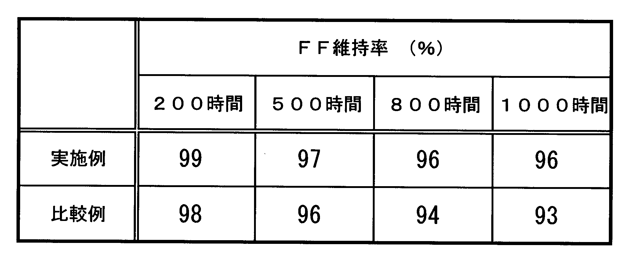
これらの結果から、特に、実施例の太陽電池素子は、比較例の太陽電池素子に比べてFFの維持率が高いことを確認した。これにより、ポリシロキサン層がアルキル基を含有することによる、太陽電池素子10の信頼性向上の効果が確認された。
1 :シリコン基板
1a:第1面
1b:第2面
1c:側面
2 :第1半導体層(p型半導体領域)
3 :第2半導体層(n型半導体領域)
4 :BSF層
5 :反射防止層
6 :第1電極
6a:第1出力取出電極
6b:第1集電電極
7 :第2電極
8 :第3電極
9 :パッシベーション層
10 :太陽電池素子
10a:第1面
10b:第2面
10c:側面
11 :保護層
12 :接続導体部
20 :シリカ層
21 :ポリシロキサン層
1a:第1面
1b:第2面
1c:側面
2 :第1半導体層(p型半導体領域)
3 :第2半導体層(n型半導体領域)
4 :BSF層
5 :反射防止層
6 :第1電極
6a:第1出力取出電極
6b:第1集電電極
7 :第2電極
8 :第3電極
9 :パッシベーション層
10 :太陽電池素子
10a:第1面
10b:第2面
10c:側面
11 :保護層
12 :接続導体部
20 :シリカ層
21 :ポリシロキサン層
Claims (13)
- 一方の表面にp型半導体領域を有する半導体基板と、
前記p型半導体領域の上に位置している、酸化アルミニウムを含んでいるパッシベーション層と、
該パッシベーション層の上に位置している、アルキル基を有するポリシロキサン層を含んでいる保護層と
を備えている太陽電池素子。 - 前記ポリシロキサン層はシリカ粒子を有している、請求項1に記載の太陽電池素子。
- 前記保護層はシリカ層をさらに含んでいる、請求項1または2に記載の太陽電池素子。
- 前記保護層の前記シリカ層は前記パッシベーション層に接している、請求項3に記載の太陽電池素子。
- 前記保護層を覆う金属層をさらに備えており、前記保護層の前記シリカ層は前記金属層に接している、請求項3または4に記載の太陽電池素子。
- 前記シリカ層は、前記パッシベーション層と前記ポリシロキサン層との間に位置している、請求項3乃至5のいずれかに記載の太陽電池素子。
- 前記シリカ層が前記ポリシロキサン層よりも薄い、請求項3乃至6のいずれかに記載の太陽電池素子。
- 前記ポリシロキサン層はカルボキシル基および炭酸基の少なくとも一方を含んでいる、請求項1乃至7のいずれかに記載の太陽電池素子。
- 一方の表面にp型半導体領域を有する半導体基板の前記p型半導体領域の上に、酸化アルミニウムを含むパッシベーション層を形成する工程と、
該パッシベーション層の上に、ポリシロキサンオリゴマーを含む塗布膜を形成する工程と、
該塗布膜を乾燥させてアルキル基を有するポリシロキサン層を含んでいる保護層を形成する工程と
を有する太陽電池素子の製造方法。 - 前記パッシベーション層を形成する工程の後で、前記塗布膜を形成する工程の前に、シリカ層を前記パッシベーション層の上に形成する工程をさらに有する、請求項9に記載の太陽電池素子の製造方法。
- 前記ポリシロキサン層に含まれるアルキル基の一部を酸化させて、前記ポリシロキサン層にカルボキシル基および炭酸基の少なくとも一方を含ませる工程をさらに有する、請求項9または10に記載の太陽電池素子の製造方法。
- 前記ポリシロキサン層はスクリーン印刷法によって形成する、請求項9乃至11のいずれかに記載の太陽電池素子の製造方法。
- 前記パッシベーション層はALD法によって形成する、請求項9乃至12のいずれかに記載の太陽電池素子の製造方法。
Priority Applications (4)
| Application Number | Priority Date | Filing Date | Title |
|---|---|---|---|
| JP2017520815A JP6203986B2 (ja) | 2015-05-27 | 2016-05-27 | 太陽電池素子およびその製造方法 |
| EP16800126.1A EP3306674B1 (en) | 2015-05-27 | 2016-05-27 | Solar cell element and method for manufacturing same |
| CN201680030373.0A CN107690709B (zh) | 2015-05-27 | 2016-05-27 | 太阳能电池元件及其制造方法 |
| US15/820,153 US10276732B2 (en) | 2015-05-27 | 2017-11-21 | Solar cell element and method of manufacturing solar cell element |
Applications Claiming Priority (2)
| Application Number | Priority Date | Filing Date | Title |
|---|---|---|---|
| JP2015-107736 | 2015-05-27 | ||
| JP2015107736 | 2015-05-27 |
Related Child Applications (1)
| Application Number | Title | Priority Date | Filing Date |
|---|---|---|---|
| US15/820,153 Continuation US10276732B2 (en) | 2015-05-27 | 2017-11-21 | Solar cell element and method of manufacturing solar cell element |
Publications (1)
| Publication Number | Publication Date |
|---|---|
| WO2016190422A1 true WO2016190422A1 (ja) | 2016-12-01 |
Family
ID=57393473
Family Applications (1)
| Application Number | Title | Priority Date | Filing Date |
|---|---|---|---|
| PCT/JP2016/065772 Ceased WO2016190422A1 (ja) | 2015-05-27 | 2016-05-27 | 太陽電池素子およびその製造方法 |
Country Status (5)
| Country | Link |
|---|---|
| US (1) | US10276732B2 (ja) |
| EP (1) | EP3306674B1 (ja) |
| JP (1) | JP6203986B2 (ja) |
| CN (1) | CN107690709B (ja) |
| WO (1) | WO2016190422A1 (ja) |
Cited By (2)
| Publication number | Priority date | Publication date | Assignee | Title |
|---|---|---|---|---|
| CN109616527A (zh) * | 2017-10-02 | 2019-04-12 | Lg电子株式会社 | 太阳能电池板及其制造方法 |
| EP3496156A1 (en) * | 2017-12-08 | 2019-06-12 | Samsung SDI Co., Ltd. | Solar cell |
Families Citing this family (3)
| Publication number | Priority date | Publication date | Assignee | Title |
|---|---|---|---|---|
| US12317637B2 (en) | 2020-12-29 | 2025-05-27 | Zhejiang Jinko Solar Co., Ltd. | Photovoltaic cell, method for manufacturing same, and photovoltaic module |
| CN114759097B (zh) * | 2020-12-29 | 2022-10-18 | 浙江晶科能源有限公司 | 太阳能电池及其制备方法、光伏组件 |
| CN112909128A (zh) * | 2021-02-07 | 2021-06-04 | 宣城睿晖宣晟企业管理中心合伙企业(有限合伙) | 异质结太阳能电池片的制造方法及异质结太阳能电池片 |
Citations (3)
| Publication number | Priority date | Publication date | Assignee | Title |
|---|---|---|---|---|
| US20120152343A1 (en) * | 2010-12-16 | 2012-06-21 | E. I. Du Pont De Nemours And Company | Aluminum paste compositions comprising siloxanes and their use in manufacturing solar cells |
| JP2013046009A (ja) * | 2011-08-26 | 2013-03-04 | Shin Etsu Chem Co Ltd | 太陽電池及びその製造方法 |
| WO2014044924A1 (en) * | 2012-09-24 | 2014-03-27 | Optitune Oy | A method of modifying an n-type silicon substrate |
Family Cites Families (12)
| Publication number | Priority date | Publication date | Assignee | Title |
|---|---|---|---|---|
| US6940177B2 (en) * | 2002-05-16 | 2005-09-06 | Dow Corning Corporation | Semiconductor package and method of preparing same |
| JP2004193350A (ja) | 2002-12-11 | 2004-07-08 | Sharp Corp | 太陽電池セルおよびその製造方法 |
| US20110114148A1 (en) * | 2003-04-11 | 2011-05-19 | Marina Temchenko | Bright white protective laminates |
| JP2007502333A (ja) * | 2003-08-01 | 2007-02-08 | ダウ・コーニング・コーポレーション | 光起電アプリケーション用のシリコーンベース誘電被膜及びフィルム |
| JP5023456B2 (ja) * | 2005-03-28 | 2012-09-12 | 大日本印刷株式会社 | 有機薄膜太陽電池素子 |
| US20070295388A1 (en) * | 2006-05-05 | 2007-12-27 | Nanosolar, Inc. | Solar assembly with a multi-ply barrier layer and individually encapsulated solar cells or solar cell strings |
| TW200929575A (en) | 2007-12-28 | 2009-07-01 | Ind Tech Res Inst | A passivation layer structure of the solar cell and the method of the fabricating |
| DE102009025977A1 (de) | 2009-06-16 | 2010-12-23 | Q-Cells Se | Solarzelle und Herstellungsverfahren einer Solarzelle |
| JP5649580B2 (ja) | 2009-09-18 | 2015-01-07 | 信越化学工業株式会社 | 太陽電池の製造方法 |
| JP5978564B2 (ja) * | 2011-05-26 | 2016-08-24 | 日立化成株式会社 | 半導体基板用パッシベーション膜形成用材料、半導体基板用パッシベーション膜及びその製造方法、並びに太陽電池素子及びその製造方法 |
| EP2533305A3 (en) | 2011-06-06 | 2014-05-21 | Imec | Method for blister-free passivation of a silicon surface |
| KR101631450B1 (ko) * | 2013-03-05 | 2016-06-17 | 엘지전자 주식회사 | 태양 전지 |
-
2016
- 2016-05-27 JP JP2017520815A patent/JP6203986B2/ja active Active
- 2016-05-27 WO PCT/JP2016/065772 patent/WO2016190422A1/ja not_active Ceased
- 2016-05-27 CN CN201680030373.0A patent/CN107690709B/zh active Active
- 2016-05-27 EP EP16800126.1A patent/EP3306674B1/en active Active
-
2017
- 2017-11-21 US US15/820,153 patent/US10276732B2/en active Active
Patent Citations (3)
| Publication number | Priority date | Publication date | Assignee | Title |
|---|---|---|---|---|
| US20120152343A1 (en) * | 2010-12-16 | 2012-06-21 | E. I. Du Pont De Nemours And Company | Aluminum paste compositions comprising siloxanes and their use in manufacturing solar cells |
| JP2013046009A (ja) * | 2011-08-26 | 2013-03-04 | Shin Etsu Chem Co Ltd | 太陽電池及びその製造方法 |
| WO2014044924A1 (en) * | 2012-09-24 | 2014-03-27 | Optitune Oy | A method of modifying an n-type silicon substrate |
Non-Patent Citations (1)
| Title |
|---|
| See also references of EP3306674A4 * |
Cited By (4)
| Publication number | Priority date | Publication date | Assignee | Title |
|---|---|---|---|---|
| CN109616527A (zh) * | 2017-10-02 | 2019-04-12 | Lg电子株式会社 | 太阳能电池板及其制造方法 |
| JP2019068070A (ja) * | 2017-10-02 | 2019-04-25 | エルジー エレクトロニクス インコーポレイティド | 太陽電池パネル及びその製造方法 |
| EP3496156A1 (en) * | 2017-12-08 | 2019-06-12 | Samsung SDI Co., Ltd. | Solar cell |
| TWI721279B (zh) * | 2017-12-08 | 2021-03-11 | 南韓商三星Sdi股份有限公司 | 太陽能電池 |
Also Published As
| Publication number | Publication date |
|---|---|
| JP6203986B2 (ja) | 2017-09-27 |
| US10276732B2 (en) | 2019-04-30 |
| US20180102441A1 (en) | 2018-04-12 |
| EP3306674A1 (en) | 2018-04-11 |
| CN107690709A (zh) | 2018-02-13 |
| EP3306674A4 (en) | 2019-01-09 |
| CN107690709B (zh) | 2019-09-24 |
| JPWO2016190422A1 (ja) | 2017-09-07 |
| EP3306674B1 (en) | 2021-06-23 |
Similar Documents
| Publication | Publication Date | Title |
|---|---|---|
| JP6285545B2 (ja) | 太陽電池素子および太陽電池モジュール | |
| CN102939662B (zh) | 太阳能电池元件及其制造方法、以及太阳能电池模块 | |
| JP6203986B2 (ja) | 太陽電池素子およびその製造方法 | |
| JP6648986B2 (ja) | 太陽電池素子および太陽電池モジュール | |
| JP6229099B1 (ja) | 絶縁性ペースト、絶縁性ペーストの製造方法、太陽電池素子の製造方法および太陽電池素子 | |
| WO2006117980A1 (ja) | 太陽電池の製造方法及び太陽電池並びに半導体装置の製造方法 | |
| JP6807433B2 (ja) | 太陽電池素子 | |
| JP6203990B1 (ja) | 太陽電池素子 | |
| TWI619259B (zh) | p型選擇射極形成方法 | |
| JP6430842B2 (ja) | 太陽電池素子の製造方法および太陽電池モジュールの製造方法 | |
| JP6555984B2 (ja) | 太陽電池素子およびその製造方法 | |
| JP6571409B2 (ja) | 太陽電池素子およびその製造方法 | |
| KR101198930B1 (ko) | 질화규소 반사방지막의 제조 방법 및 이를 이용한 실리콘 태양전지 | |
| US20190245107A1 (en) | Solar cell element | |
| JP6224513B2 (ja) | 太陽電池素子の製造方法 | |
| CN107360731B (zh) | 太阳能电池元件及其制造方法 | |
| KR101133953B1 (ko) | 실리카 반사방지막의 제조 방법 및 이를 이용한 실리콘 태양전지 | |
| JP6539010B1 (ja) | 太陽電池素子 |
Legal Events
| Date | Code | Title | Description |
|---|---|---|---|
| 121 | Ep: the epo has been informed by wipo that ep was designated in this application |
Ref document number: 16800126 Country of ref document: EP Kind code of ref document: A1 |
|
| ENP | Entry into the national phase |
Ref document number: 2017520815 Country of ref document: JP Kind code of ref document: A |
|
| NENP | Non-entry into the national phase |
Ref country code: DE |
|
| WWE | Wipo information: entry into national phase |
Ref document number: 2016800126 Country of ref document: EP |