WO2016194515A1 - 光走査制御装置 - Google Patents
光走査制御装置 Download PDFInfo
- Publication number
- WO2016194515A1 WO2016194515A1 PCT/JP2016/062824 JP2016062824W WO2016194515A1 WO 2016194515 A1 WO2016194515 A1 WO 2016194515A1 JP 2016062824 W JP2016062824 W JP 2016062824W WO 2016194515 A1 WO2016194515 A1 WO 2016194515A1
- Authority
- WO
- WIPO (PCT)
- Prior art keywords
- light
- optical scanning
- control device
- microlenses
- screen
- Prior art date
- Legal status (The legal status is an assumption and is not a legal conclusion. Google has not performed a legal analysis and makes no representation as to the accuracy of the status listed.)
- Ceased
Links
Images




Classifications
-
- G—PHYSICS
- G02—OPTICS
- G02B—OPTICAL ELEMENTS, SYSTEMS OR APPARATUS
- G02B26/00—Optical devices or arrangements for the control of light using movable or deformable optical elements
- G02B26/08—Optical devices or arrangements for the control of light using movable or deformable optical elements for controlling the direction of light
- G02B26/10—Scanning systems
-
- G—PHYSICS
- G02—OPTICS
- G02B—OPTICAL ELEMENTS, SYSTEMS OR APPARATUS
- G02B26/00—Optical devices or arrangements for the control of light using movable or deformable optical elements
- G02B26/08—Optical devices or arrangements for the control of light using movable or deformable optical elements for controlling the direction of light
- G02B26/10—Scanning systems
- G02B26/101—Scanning systems with both horizontal and vertical deflecting means, e.g. raster or XY scanners
-
- G—PHYSICS
- G02—OPTICS
- G02B—OPTICAL ELEMENTS, SYSTEMS OR APPARATUS
- G02B27/00—Optical systems or apparatus not provided for by any of the groups G02B1/00 - G02B26/00, G02B30/00
- G02B27/01—Head-up displays
-
- G—PHYSICS
- G02—OPTICS
- G02B—OPTICAL ELEMENTS, SYSTEMS OR APPARATUS
- G02B27/00—Optical systems or apparatus not provided for by any of the groups G02B1/00 - G02B26/00, G02B30/00
- G02B27/48—Laser speckle optics
-
- G—PHYSICS
- G02—OPTICS
- G02B—OPTICAL ELEMENTS, SYSTEMS OR APPARATUS
- G02B3/00—Simple or compound lenses
- G02B3/0006—Arrays
- G02B3/0037—Arrays characterized by the distribution or form of lenses
- G02B3/0043—Inhomogeneous or irregular arrays, e.g. varying shape, size, height
-
- G—PHYSICS
- G02—OPTICS
- G02B—OPTICAL ELEMENTS, SYSTEMS OR APPARATUS
- G02B3/00—Simple or compound lenses
- G02B3/0006—Arrays
- G02B3/0037—Arrays characterized by the distribution or form of lenses
- G02B3/0056—Arrays characterized by the distribution or form of lenses arranged along two different directions in a plane, e.g. honeycomb arrangement of lenses
-
- G—PHYSICS
- G03—PHOTOGRAPHY; CINEMATOGRAPHY; ANALOGOUS TECHNIQUES USING WAVES OTHER THAN OPTICAL WAVES; ELECTROGRAPHY; HOLOGRAPHY
- G03B—APPARATUS OR ARRANGEMENTS FOR TAKING PHOTOGRAPHS OR FOR PROJECTING OR VIEWING THEM; APPARATUS OR ARRANGEMENTS EMPLOYING ANALOGOUS TECHNIQUES USING WAVES OTHER THAN OPTICAL WAVES; ACCESSORIES THEREFOR
- G03B21/00—Projectors or projection-type viewers; Accessories therefor
- G03B21/54—Accessories
- G03B21/56—Projection screens
-
- G—PHYSICS
- G03—PHOTOGRAPHY; CINEMATOGRAPHY; ANALOGOUS TECHNIQUES USING WAVES OTHER THAN OPTICAL WAVES; ELECTROGRAPHY; HOLOGRAPHY
- G03B—APPARATUS OR ARRANGEMENTS FOR TAKING PHOTOGRAPHS OR FOR PROJECTING OR VIEWING THEM; APPARATUS OR ARRANGEMENTS EMPLOYING ANALOGOUS TECHNIQUES USING WAVES OTHER THAN OPTICAL WAVES; ACCESSORIES THEREFOR
- G03B21/00—Projectors or projection-type viewers; Accessories therefor
- G03B21/54—Accessories
- G03B21/56—Projection screens
- G03B21/60—Projection screens characterised by the nature of the surface
- G03B21/62—Translucent screens
Definitions
- the present invention relates to an optical scanning control device.
- An optical scanning control device that scans a laser beam and displays an image is known.
- a microlens array may be used as a screen.
- an interference pattern may be visually recognized due to the regularity of the lens arrangement.
- it has first and second microlens array portions in which a plurality of microlenses are arranged, and the interval between the microlenses arranged in the first microlens array portion is set to the second microlens array portion. It has been proposed that the distance between the microlenses arranged in the lens array portion is narrower (see, for example, Patent Document 1).
- two microlens arrays are required, and there is a problem that the cost increases.
- an object of an embodiment of the present invention is to provide an optical scanning control apparatus capable of reducing speckle noise and interference patterns while suppressing an increase in cost.
- the optical scanning control device (1) is scanned by scanning means (310) for scanning light emitted from lasers (211R, 211G, 211B) and the scanning means (310). And a screen (50) on which the light is imaged.
- a plurality of microlenses (50m) are arranged on at least one of the light incident side and the light emitting side of the screen (50).
- Each of the microlenses (50m) is arranged with a center-to-center distance at random in at least one of a first direction and a second direction orthogonal to the first direction.
- an optical scanning control device capable of reducing speckle noise and interference patterns while suppressing an increase in cost.
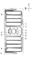
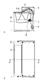
- FIG. 1 is an external view (part 1) illustrating an optical scanning control device according to an embodiment; It is an external view (the 2) which illustrates the optical scanning control apparatus which concerns on this Embodiment.
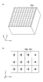
- FIG. (The 1) which illustrates the microlens array which concerns on a comparative example.
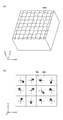
- FIG. (The 1) which illustrates the microlens array which concerns on this Embodiment.
- FIG. (1) explaining a reference distance.
- FIG. (The 2) which illustrates the microlens array which concerns on a comparative example.
- FIG. 4 is a second diagram illustrating a microlens array according to the embodiment; It is FIG. (2) explaining a reference distance.
- FIG. 1 is a block diagram illustrating an optical scanning control apparatus according to this embodiment.
- FIG. 2 is a plan view illustrating an optical scanning unit constituting the optical scanning control device.
- 3 and 4 are external views illustrating the optical scanning control apparatus according to this embodiment.
- the optical scanning control device 1 includes, as main components, a circuit unit 10, a light source unit 20, an optical scanning unit 30, an optical unit 40, a screen 50, and a light quantity detection sensor 60. It is stored in the body 100.
- the optical scanning control device 1 is, for example, a laser scanning projector.
- the circuit unit 10 is a part that controls the light source unit 20 and the optical scanning unit 30, and can be configured by, for example, a system controller 11, a CPU (Central Processing Unit) 12, various driving circuits, and the like.
- a system controller 11 a CPU (Central Processing Unit) 12, various driving circuits, and the like.
- CPU Central Processing Unit
- the light source unit 20 includes an LD module 21, a temperature control unit 22, a temperature sensor 23, and a neutral density filter 24.
- the LD module 21 includes lasers 211R, 211G, and 211B that change the amount of light emitted according to the current value, a light amount detection sensor 215 that monitors the most recent light amounts of the lasers 211R, 211G, and 211B, and the like.
- the laser 211R is, for example, a red semiconductor laser, and can emit light having a wavelength ⁇ R (for example, 640 nm).
- the laser 211G is, for example, a green semiconductor laser, and can emit light having a wavelength ⁇ G (for example, 530 nm).
- the laser 211B is, for example, a blue semiconductor laser, and can emit light having a wavelength ⁇ B (for example, 445 nm).
- As the light quantity detection sensor 215, for example, a photodiode or the like can be used.
- the light quantity detection sensor 215 can be disposed at an arbitrary position where the light quantity before passing through the neutral density filter 24 can be detected.
- the temperature control unit 22 can control the lasers 211R, 211G, and 211B to a predetermined temperature.
- the temperature sensor 23 can detect the temperatures of the lasers 211R, 211G, and 211B.
- a Peltier element can be used.
- a thermistor can be used.
- the neutral density filter 24 is disposed in front of the mirror 310, and the light (the combined light) emitted from the lasers 211R, 211G, and 211B is incident thereon.
- the neutral density filter 24 has a function of adjusting the luminance on the screen 50.
- an ND (Neutral-Density) filter, a liquid crystal element, a polarizing filter, or the like can be used as the neutral density filter 24.
- the neutral density filter 24 is inserted to be inclined with respect to the optical axis of incident light, and light that is not transmitted (light that is attenuated) is absorbed or reflected by the neutral density filter 24.
- the optical scanning unit 30 is, for example, a MEMS (Micro Electro Mechanical System) that drives the mirror 310 with a piezoelectric element.
- the mirror 310 reflects the light (combined light) emitted from the lasers 211R, 211G, and 211B, scans the incident light in two dimensions in the horizontal and vertical directions according to the video signal, and couples it to the screen 50. It functions as scanning means for imaging.
- the mirror 310 is supported from both sides by torsion beams 331 and 332 constituting an axis.
- Drive beams 351 and 352 are provided in pairs so as to sandwich the mirror 310 in a direction orthogonal to the torsion beams 331 and 332.
- the mirror 310 can be swung around the axis with the torsion beams 331 and 332 as axes.
- the direction in which the mirror 310 swings about the axes of the torsion beams 331 and 332 is hereinafter referred to as the horizontal direction.
- the horizontal displacement sensor 391 is a sensor that detects the horizontal tilt of the mirror 310 when the mirror 310 is oscillating in the horizontal direction.
- driving beams 371 and 372 are provided in pairs outside the driving beams 351 and 352.
- the piezoelectric element formed on each surface of the drive beams 371 and 372 can swing the mirror 310 in the vertical direction, which is a direction orthogonal to the horizontal direction.
- the vertical displacement sensors 395 and 396 are sensors that detect the vertical inclination of the mirror 310 in a state where the mirror 310 is swinging in the vertical direction.
- the optical scanning unit 30 is mounted on a ceramic package together with a drive circuit and the like, and is covered with a ceramic cover.
- the optical unit 40 is an optical system for projecting the light scanned by the light scanning unit 30 onto the screen 50.
- the mirror 43, the concave mirror 44, etc. can be included.
- a lens may be used instead of the reflecting mirror.
- the light incident on the optical unit 40 from the optical scanning unit 30 is converted into substantially parallel light by the concave mirror 44 and forms an image on the screen 50, and an image corresponding to the video signal is drawn on the screen 50.
- the screen 50 is provided with a microlens array in order to remove noise in a granular image called speckle.
- a microlens array corresponds to a pixel of the display, and it is desirable that the irradiated laser beam is equal to or smaller than the size of the microlens. Details of the microlens array constituting the screen 50 will be described later.
- the light quantity detection sensor 60 can be disposed at any position where the light quantity after passing through the neutral density filter 24 can be detected.
- the light amount detection sensor 60 can independently detect the light amounts of the lasers 211R, 211G, and 211B after passing through the neutral density filter 24.
- the light quantity detection sensor 60 for example, one or a plurality of photodiodes can be used.
- the system controller 11 can control the deflection angle of the mirror 310.
- the system controller 11 monitors, for example, the horizontal and vertical inclinations of the mirror 310 obtained by the horizontal displacement sensor 391 and the vertical displacement sensors 395 and 396 via the buffer circuit 13, and sends an angle control signal to the mirror drive circuit 14.
- the mirror drive circuit 14 supplies a predetermined drive signal to the drive beams 351 and 352 and the drive beams 371 and 372 based on the angle control signal from the system controller 11 to drive (scan) the mirror 310 at a predetermined angle. can do.
- the system controller 11 can supply a digital video signal to the laser drive circuit 15, for example.
- the laser drive circuit 15 supplies a predetermined current to the lasers 211R, 211G, and 211B based on the video signal from the system controller 11. Accordingly, the lasers 211R, 211G, and 211B emit red, green, and blue light modulated according to the video signal, and a color image can be formed by combining these light.
- the CPU 12 can monitor the emitted light quantity at the base of the lasers 211R, 211G, and 211B by the output of the light quantity detection sensor 215 and supply a light quantity control signal to the LD module 21, for example.
- the lasers 211 ⁇ / b> R, 211 ⁇ / b> G, and 211 ⁇ / b> B are current-controlled so as to obtain a predetermined output (light quantity) based on the light quantity control signal from the CPU 12.
- the light amount detection sensor 215 can include three sensors that independently detect the emitted light amounts of the lasers 211R, 211G, and 211B.
- the light amount detection sensor 215 may be composed of only one sensor.
- the emitted light amounts of the lasers 211R, 211G, and 211B can be controlled by sequentially emitting the lasers 211R, 211G, and 211B and sequentially detecting them with one sensor.
- the CPU 12 can monitor the temperatures of the lasers 211 R, 211 G, and 211 B based on the output of the temperature sensor 23 and supply a temperature control signal to the temperature control circuit 16. Then, the temperature control circuit 16 supplies a predetermined current to the temperature control unit 22 based on the temperature control signal from the CPU 12. Thereby, the temperature control part 22 is heated or cooled, and it can control so that each laser may become predetermined
- the light quantity detection sensor 60 detects the light quantity after passing through the neutral density filter 24.
- the light amount detection sensor 215 for adjusting the light amount of each laser is mounted in the LD module 21 and is the root of the lasers 211R, 211G, and 211B (before passing through the neutral density filter 24). ) The amount of emitted light is detected.
- the image actually displayed by the optical scanning control device 1 is based on the light imaged on the screen 50, there is a case where correct adjustment cannot be performed by adjustment based on the laser light quantity at the base.
- the neutral density filter 24 since the neutral density filter 24 is provided on the optical path, the expected attenuation ratio cannot be obtained depending on the characteristics of the neutral density filter 24. Therefore, the amount of light after passing through the neutral density filter 24 is as expected. It may not be possible. Further, when there is a variation in the R / G / B dimming ratio of the neutral density filter 24, the white balance after passing through the neutral density filter 24 may be lost. Further, the characteristics of the optical scanning unit 30 may fluctuate due to temperature and aging degradation. Such a problem cannot be solved no matter how precisely the amount of light before passing through the optical scanning unit 30 is controlled by the light amount detection sensor 215.
- a light quantity detection sensor 60 is provided as a light quantity detection means for detecting the light quantity after passing through the neutral density filter 24.
- the detection result of the light quantity detection sensor 60 is input to the CPU 12 which is a control means, and the CPU 12 supplies a light quantity control signal for controlling the current value of each laser to the LD module 21 based on the light quantity detected by the light quantity detection sensor 60. Can do.
- the light amount detection sensor 60 can independently detect the respective light amounts of the lasers 211R, 211G, and 211B, and the CPU 12 determines the current values of the respective lasers based on the respective light amounts detected by the light amount detection sensor 60. Can be controlled.
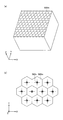
- FIG. 5 is a diagram (part 1) illustrating a microlens array (conventional microlens array) according to a comparative example
- FIG. 5A is a perspective view
- FIG. 5B is a center position of each microlens. It is the top view which showed typically.
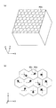
- FIG. 6 is a diagram (part 1) illustrating the microlens array according to the present embodiment, where FIG. 6A is a perspective view, and FIG. 6B is a schematic view of the center position of each microlens. It is the top view shown in.
- each microlens 500m is a quadrangle
- the center 500c of each microlens 500m is orthogonal to the X direction (lateral direction) and the X direction. They are arranged at equal intervals in the Y direction (vertical direction).
- the centers 50c of the microlenses 50m are arranged with randomness in the X direction and the Y direction. That is, the micro lenses 50m are arranged at random distances between the centers in the X direction and the Y direction (arranged at different intervals in the X direction and the Y direction).
- the surface of the screen 50 on which the microlens array is formed can be only the surface on either the light incident side or the light emitting side. Even if the microlens array is formed on any surface, the effect of reducing the interference pattern while maintaining the speckle reduction function described later is equivalent. However, it is preferable to form the microlens array on the light incident side in that a smooth image can be visually recognized from the light emitting side. The same effect can be obtained when microlens arrays are formed on both the light incident side and the light exiting side and the arrangement of microlenses on at least one surface is random.
- each microlens 50m of FIG. 6B the intersection of the cross lines indicates the position where the center 500c of FIG. 5B is located, and the arrow indicates that the center 50c is located with respect to the center 500c of FIG. The shifted direction is shown.
- each microlens 50m may be either spherical or aspherical, but the thickness and radius of curvature of each microlens 50m are unified in any case. Thereby, the focal distance of each micro lens 50m can be made equal.
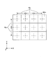
- FIG. 7 is a diagram (part 1) for explaining the reference distance, and is a plan view schematically illustrating a microlens array.
- the intersection of the cross lines indicates the position when the centers of the microlenses 50m are arranged at equal intervals in the X direction and the Y direction.
- the distance between the centers of adjacent microlenses 50m in the X direction is defined as a reference distance Rx
- the distance between the centers of adjacent microlenses 50m in the Y direction is defined as a reference distance Ry.
- the reference distance Rx and the reference distance Ry can be appropriately determined according to the required specifications, but can be, for example, about several tens to several hundreds ⁇ m.
- each micro lens 50m is arranged for each of the reference distance Rx and the reference distance Ry, and this becomes the standard dimension of the micro lens 50m.
- the reference distance Rx and the reference distance Ry may be the same or different.
- each microlens 50m The center coordinates of are shown in Table 1.
- the average size of each micro lens 50m becomes substantially equal to the reference distance Rx and the reference distance Ry. Therefore, the diffusion angle of the screen 50 can be obtained from the numerical aperture NA (Numerical Aperture) of the lens whose size is determined by the reference distance Rx and the reference distance Ry.
- NA numerical aperture
- the amount of deviation is desirably 30% or less with respect to the reference distance Rx and the reference distance Ry, as studied by the inventors. That is, it is desirable that ⁇ x / Rx ⁇ 30% and ⁇ y / Ry ⁇ 30%. As a result, it is possible to reduce the interference pattern while maintaining the speckle reduction function.
- planar shape of the microlens is a quadrangle (in the case of a square array arranged in a grid) has been described with reference to FIGS. 5 to 7, it is not limited to this.
- the planar shape of the microlens may be a hexagonal shape (triangular arrangement arranged in a honeycomb shape), or may be a planar shape other than these.
- FIG. 9 to 10 show the case where the planar shape of the microlens 500m is hexagonal.
- FIG. 9 is a diagram (part 2) illustrating a microlens array (conventional microlens array) according to a comparative example.
- FIG. 9A is a perspective view
- FIG. 9B is a center position of each microlens. It is the top view which showed typically.
- FIG. 10 is a diagram (part 2) illustrating the microlens array according to this embodiment.
- FIG. 10A is a perspective view
- FIG. 10B is a schematic view of the center position of each microlens. It is the top view shown in.
- FIG. 11 is a diagram (part 2) for explaining the reference distance, and is a plan view schematically illustrating a microlens array.
- the center 50c of each microlens 50m is random in the X direction and the Y direction by the same method as when the planar shape of the microlens 500m is a square. Can be arranged. It is desirable that the deviation amount distribution is a normal distribution or a uniform distribution, and the deviation amount is desirably 30% or less with respect to the reference distance Rx and the reference distance Ry (that is, ⁇ x / Rx ⁇ The same applies to 30% and ⁇ y / Ry ⁇ 30%.
- the screen 50 is constituted by the microlens array 50m, and the center 50c of each microlens 50m is arranged with randomness in the X direction and the Y direction, so that the interference pattern is maintained while maintaining the speckle reduction function. Can be reduced.
- the center 50c of each micro lens 50m is arranged with randomness in only one of the X direction and the Y direction, it is possible to reduce the interference pattern while maintaining the speckle reduction function. Become.
- the spot diameter (FWHM: half width) of the light beam irradiated on the screen 50 is preferably smaller than the reference distance Rx and the reference distance Ry. If the spot diameter of the light beam applied to the screen 50 is larger than the reference distance Rx and the reference distance Ry, the probability that the light beam is applied across the plurality of microlenses 50m increases, and interference patterns are likely to occur. is there.
- optical scanning control device for example, in the above-described embodiment, an example in which the optical scanning control device according to the present invention is applied to a laser scanning projector has been described.
- the optical scanning control device according to the present invention is not limited to the above example.
- the optical scanning control device according to the present invention can be applied to various devices that display an image on a screen. Examples of such devices include an on-vehicle head-up display, a laser printer, a laser scanning epilator, a laser head lamp, and a laser radar.
- an in-vehicle head-up display with reduced speckle noise and interference patterns can be constructed by using the screen of the optical scanning control device according to the present invention as an intermediate screen and indirectly projecting an image on a windshield or a combiner.
Landscapes
- Physics & Mathematics (AREA)
- General Physics & Mathematics (AREA)
- Optics & Photonics (AREA)
- Mechanical Optical Scanning Systems (AREA)
- Overhead Projectors And Projection Screens (AREA)
- Mechanical Light Control Or Optical Switches (AREA)
Abstract
レーザから出射された光を走査する走査手段と、前記走査手段により走査された光が結像するスクリーンと、を有する光走査制御装置。前記スクリーンの光の入射側若しくは出射側の少なくとも一方の面に複数のマイクロレンズが配列されている。 夫々の前記マイクロレンズは、第1の方向、前記第1の方向と直交する第2の方向の少なくとも1方向において、中心間距離をランダムにして配列されている。
Description
本発明は、光走査制御装置に関する。
レーザ光を走査して画像を表示する光走査制御装置が知られている。このような光制御装置において、スペックルノイズによる影響を抑制するために、スクリーンとしてマイクロレンズアレイを用いる場合がある。
しかしながら、スクリーンとしてマイクロレンズアレイを用いると、レンズ配列の規則性のために、干渉模様が視認される場合がある。これを防止するために、例えば、複数のマイクロレンズが配列された第1及び第2マイクロレンズアレイ部を有し、第1マイクロレンズアレイ部に配列されたマイクロレンズ同士の間隔を、第2マイクロレンズアレイ部に配列されたマイクロレンズ同士の間隔よりも狭く構成することが提案されている(例えば、特許文献1参照)。しかしながら、上記の光走査制御装置では、2枚のマイクロレンズアレイが必要となるため、コストが上昇するという問題があった。
しかしながら、スクリーンとしてマイクロレンズアレイを用いると、レンズ配列の規則性のために、干渉模様が視認される場合がある。これを防止するために、例えば、複数のマイクロレンズが配列された第1及び第2マイクロレンズアレイ部を有し、第1マイクロレンズアレイ部に配列されたマイクロレンズ同士の間隔を、第2マイクロレンズアレイ部に配列されたマイクロレンズ同士の間隔よりも狭く構成することが提案されている(例えば、特許文献1参照)。しかしながら、上記の光走査制御装置では、2枚のマイクロレンズアレイが必要となるため、コストが上昇するという問題があった。
上記の課題に鑑みて、本発明の一実施例は、コスト上昇を抑制しつつスペックルノイズ及び干渉模様を低減することが可能な光走査制御装置を提供することを目的とする。
本発明の一実施例では、本光走査制御装置(1)は、レーザ(211R、211G、211B)から出射された光を走査する走査手段(310)と、前記走査手段(310)により走査された光が結像するスクリーン(50)と、を有する。前記スクリーン(50)の光の入射側若しくは出射側の少なくとも一方の面に複数のマイクロレンズ(50m)が配列されている。夫々の前記マイクロレンズ(50m)は、第1の方向、前記第1の方向と直交する第2の方向の少なくとも1方向において、中心間距離をランダムにして配列されている。
なお、上記括弧内の参照符号は、理解を容易にするために付したものであり、一例にすぎず、図示の態様に限定されるものではない。
本発明の実施例によれば、コスト上昇を抑制しつつスペックルノイズ及び干渉模様を低減することが可能な光走査制御装置を提供できる。
以下、図面を参照して発明を実施するための形態について説明する。各図面において、同一構成部分には同一符号を付し、重複した説明を省略する場合がある。
図1は、本実施の形態に係る光走査制御装置を例示するブロック図である。図2は、光走査制御装置を構成する光走査部を例示する平面図である。図3及び図4は、本実施の形態に係る光走査制御装置を例示する外観図である。
(光走査制御装置の概略構成)
まず、図1~図4を参照して、光走査制御装置1の概略構成について説明する。光走査制御装置1は、主要な構成要素として、回路部10と、光源部20と、光走査部30と、光学部40と、スクリーン50と、光量検出センサ60とを有し、これらは筐体100に格納されている。光走査制御装置1は、例えば、レーザ走査型プロジェクタである。
まず、図1~図4を参照して、光走査制御装置1の概略構成について説明する。光走査制御装置1は、主要な構成要素として、回路部10と、光源部20と、光走査部30と、光学部40と、スクリーン50と、光量検出センサ60とを有し、これらは筐体100に格納されている。光走査制御装置1は、例えば、レーザ走査型プロジェクタである。
回路部10は、光源部20や光走査部30を制御する部分であり、例えば、システムコントローラ11やCPU(Central Processing Unit)12、各種駆動回路等により構成することができる。
光源部20は、LDモジュール21と、温度制御部22と、温度センサ23と、減光フィルタ24とを有する。
LDモジュール21は、電流値に応じて出射する光量が変化するレーザ211R、211G、及び211Bや、レーザ211R、211G、及び211Bの夫々の直近の光量をモニタする光量検出センサ215等を備えている。レーザ211Rは、例えば、赤色半導体レーザであり、波長λR(例えば、640nm)の光を出射することができる。レーザ211Gは、例えば、緑色半導体レーザであり、波長λG(例えば、530nm)の光を出射することができる。レーザ211Bは、例えば、青色半導体レーザであり、波長λB(例えば、445nm)の光を出射することができる。光量検出センサ215としては、例えば、フォトダイオード等を用いることができる。光量検出センサ215は、減光フィルタ24を通過前の光量を検出できる任意の位置に配置することができる。
温度制御部22は、レーザ211R、211G、及び211Bを所定の温度に制御することができる。温度センサ23は、レーザ211R、211G、及び211Bの夫々の温度を検出することができる。温度制御部22としては、例えば、ペルチェ素子を用いることができる。温度センサ23としては、例えば、サーミスタを用いることができる。
減光フィルタ24は、ミラー310の前段に配置され、レーザ211R、211G、及び211Bから出射された光(合成後の光)が入射する。減光フィルタ24は、スクリーン50上の輝度を調整する機能を有する。減光フィルタ24としては、ND(Neutral Density)フィルタや液晶素子、偏光フィルタ等を用いることができる。減光フィルタ24は、入射光の光軸に対して傾けて挿入され、透過しない光(減光される光)は、減光フィルタ24によって吸収若しくは反射される。
光走査部30は、例えば、圧電素子によりミラー310を駆動させるMEMS(Micro Electro Mechanical System)である。ミラー310は、レーザ211R、211G、及び211Bから出射された光(合成後の光)を反射させ、映像信号に応じて入射光を水平方向及び垂直方向の2次元に走査してスクリーン50に結像させる走査手段として機能する。
具体的には、図2に示すように、ミラー310は、軸を構成する捻れ梁331及び332により両側から支持されている。捻れ梁331及び332と直交する方向に、ミラー310を挟むように、駆動梁351及び352が対をなして設けられている。駆動梁351及び352の夫々の表面に形成された圧電素子により、捻れ梁331及び332を軸として、ミラー310を軸周りに揺動させることができる。ミラー310が捻れ梁331及び332の軸周りに揺動する方向を、以後、水平方向と呼ぶ。駆動梁351及び352による水平駆動には、例えば共振振動が用いられ、高速にミラー310を駆動することができる。水平変位センサ391は、ミラー310が水平方向に揺動している状態におけるミラー310の水平方向の傾き具合を検出するセンサである。
又、駆動梁351及び352の外側には、駆動梁371及び372が対をなして設けられている。駆動梁371及び372の夫々の表面に形成された圧電素子により、ミラー310を水平方向と直交する方向である垂直方向に揺動させることができる。垂直変位センサ395及び396は、ミラー310が垂直方向に揺動している状態におけるミラー310の垂直方向の傾き具合を検出するセンサである。なお、光走査部30は、例えば、ユニット150(図3(b)参照)において、駆動回路等と共にセラミックパッケージに搭載され、セラミックカバーに覆われている。
光学部40は、光走査部30にて走査された光をスクリーン50に投射するための光学系であり、例えば、図3(b)等に示すように、反射ミラー41、反射ミラー42、反射ミラー43、凹面ミラー44等を含んで構成することができる。但し、必要に応じ、反射ミラーに代えてレンズを用いてもよい。光走査部30から光学部40に入射した光は、凹面ミラー44により略平行光とされてスクリーン50に結像し、スクリーン50に映像信号に応じた画像が描画される。
スクリーン50は、スペックルと呼ばれる粒状に見える画像のノイズを除去するため、マイクロレンズアレイを備えている。マイクロレンズアレイを構成する各マイクロレンズは、ディスプレイの画素に相当し、照射されるレーザビームはマイクロレンズのサイズに比べて等しいか、より小さいことが望ましい。スクリーン50を構成するマイクロレンズアレイの詳細については後述する。
光量検出センサ60は、減光フィルタ24を通過後の光量を検出できる任意の位置に配置することができる。光量検出センサ60は、減光フィルタ24を通過後のレーザ211R、211G、及び211Bの夫々の光量を独立に検出可能である。光量検出センサ60としては、例えば、1つ又は複数のフォトダイオード等を用いることができる。
(光走査制御装置の概略動作)
次に、光走査制御装置1の概略動作について説明する。システムコントローラ11は、例えば、ミラー310の振れ角制御を行うことができる。システムコントローラ11は、例えば、水平変位センサ391、垂直変位センサ395及び396で得られるミラー310の水平方向及び垂直方向の傾きをバッファ回路13を介してモニタし、ミラー駆動回路14に角度制御信号を供給することができる。そして、ミラー駆動回路14は、システムコントローラ11からの角度制御信号に基づいて、駆動梁351及び352、駆動梁371及び372に所定の駆動信号を供給し、ミラー310を所定角度に駆動(走査)することができる。
次に、光走査制御装置1の概略動作について説明する。システムコントローラ11は、例えば、ミラー310の振れ角制御を行うことができる。システムコントローラ11は、例えば、水平変位センサ391、垂直変位センサ395及び396で得られるミラー310の水平方向及び垂直方向の傾きをバッファ回路13を介してモニタし、ミラー駆動回路14に角度制御信号を供給することができる。そして、ミラー駆動回路14は、システムコントローラ11からの角度制御信号に基づいて、駆動梁351及び352、駆動梁371及び372に所定の駆動信号を供給し、ミラー310を所定角度に駆動(走査)することができる。
又、システムコントローラ11は、例えば、ディジタルの映像信号をレーザ駆動回路15に供給することができる。そして、レーザ駆動回路15は、システムコントローラ11からの映像信号に基づいて、レーザ211R、211G、及び211Bに所定の電流を供給する。これにより、レーザ211R、211G、及び211Bが映像信号に応じて変調された赤色、緑色、及び青色の光を発し、これらを合成することでカラーの画像を形成することができる。
CPU12は、例えば、レーザ211R、211G、及び211Bの根元の出射光量を光量検出センサ215の出力によりモニタし、LDモジュール21に光量制御信号を供給することができる。レーザ211R、211G、及び211Bは、CPU12からの光量制御信号に基づいて、所定の出力(光量)になるように電流制御される。
なお、光量検出センサ215は、レーザ211R、211G、及び211Bの出射光量を独立に検出する3つのセンサを含む構成とすることができる。或いは、光量検出センサ215は、1つのセンサのみから構成してもよい。この場合には、レーザ211R、211G、及び211Bを順次発光させて、1つのセンサで順次検出することで、レーザ211R、211G、及び211Bの出射光量の制御が可能となる。
又、CPU12は、レーザ211R、211G、及び211Bの温度を温度センサ23の出力によりモニタし、温度制御回路16に温度制御信号を供給することができる。そして、温度制御回路16は、CPU12から温度制御信号に基づいて、温度制御部22に所定の電流を供給する。これにより、温度制御部22が加熱又は冷却され、各レーザが所定の温度になるように制御することができる。
光量検出センサ60は、減光フィルタ24を通過後の光量を検出する。前述のように、各レーザの光量調整を実施するための光量検出センサ215はLDモジュール21の中に実装されており、レーザ211R、211G、及び211Bの根元の(減光フィルタ24を通過前の)出射光量を検出している。しかしながら、光走査制御装置1で実際に表示される画像はスクリーン50に結像した光によるので、根元のレーザ光量による調整では正しい調整ができない場合がある。
例えば、光路上に減光フィルタ24を設けているので、減光フィルタ24の特性によっては、期待通りの減光比が得られないことから、減光フィルタ24を通過後の光量が期待通りにならない場合がある。又、減光フィルタ24のR/G/B夫々の減光比にばらつきがある場合に至っては、減光フィルタ24を通過後のホワイトバランスが崩れてしまうおそれがある。又、温度や経年劣化により、光走査部30の特性が変動する場合もある。このような問題は、光量検出センサ215により、光走査部30を通過前の光量を如何に精密に制御しても解決することはできない。
そこで、光走査制御装置1では、減光フィルタ24を通過後の光量を検出する光量検出手段として、光量検出センサ60を設けている。光量検出センサ60の検出結果は制御手段であるCPU12に入力され、CPU12は光量検出センサ60で検出した光量に基づいて、各レーザの電流値を制御する光量制御信号をLDモジュール21に供給することができる。
これにより、減光フィルタ24や光走査部30の特性の変動を含めたレーザ光の光量を検出できるため、スクリーン50に実際に表示される画像に対応した正確な光量制御を行うことが可能となる。なお、光量検出センサ60は、レーザ211R、211G、及び211Bの夫々の光量を独立に検出可能であり、CPU12は、光量検出センサ60で検出した夫々の光量に基づいて、夫々のレーザの電流値を制御すことができる。
(マイクロレンズアレイ)
以下、スクリーン50のマイクロレンズアレイについて詳説する。図5は、比較例に係るマイクロレンズアレイ(従来のマイクロレンズアレイ)を例示する図(その1)であり、図5(a)は斜視図、図5(b)は各マイクロレンズの中心位置を模式的に示した平面図である。又、図6は、本実施の形態に係るマイクロレンズアレイを例示する図(その1)であり、図6(a)は斜視図、図6(b)は各マイクロレンズの中心位置を模式的に示した平面図である。
以下、スクリーン50のマイクロレンズアレイについて詳説する。図5は、比較例に係るマイクロレンズアレイ(従来のマイクロレンズアレイ)を例示する図(その1)であり、図5(a)は斜視図、図5(b)は各マイクロレンズの中心位置を模式的に示した平面図である。又、図6は、本実施の形態に係るマイクロレンズアレイを例示する図(その1)であり、図6(a)は斜視図、図6(b)は各マイクロレンズの中心位置を模式的に示した平面図である。
図5に示すように、従来のマイクロレンズアレイは、例えば、個々のマイクロレンズ500mの平面形状が四角形であり、各マイクロレンズ500mの中心500cが、X方向(横方向)及びX方向と直交するY方向(縦方向)に等間隔で配置されている。
これに対して、図6に示すように、本実施の形態に係るマイクロレンズアレイは、各マイクロレンズ50mの中心50cが、X方向及びY方向にランダム性を持って配置されている。つまり、各マイクロレンズ50mは、X方向及びY方向において、中心間距離をランダムにして配列されている(X方向及びY方向に異なる間隔で配置されている)。
スクリーン50においてマイクロレンズアレイが形成される面は、光の入射側若しくは出射側の何れかの面のみとすることができる。マイクロレンズアレイを何れの面に形成しても、後述のスペックル低減機能を保持しつつ干渉模様を低減する効果は同等である。但し、マイクロレンズアレイを光の入射側に形成すると、光の出射側から滑らかな画像を視認できる点で好適である。なお、光の入射側及び出射側の両面にマイクロレンズアレイを形成し、少なくとも一方の面のマイクロレンズの配置をランダムとした場合にも同様の効果が得られる。
図6(b)の各マイクロレンズ50mにおいて、十字線の交点は図5(b)の中心500cがあった位置を示しており、矢印は図5(a)の中心500cに対して中心50cがずれた方向を示している。
なお、各マイクロレンズ50mの曲率は球面形状、非球面形状の何れであってもよいが、何れの場合も各マイクロレンズ50mの厚み及び曲率半径は統一される。これにより、各マイクロレンズ50mの焦点距離を等しくすることができる。
次に、各マイクロレンズ50mの中心50cをランダム性を持って配置する手法について説明する。図7は、基準距離について説明する図(その1)であり、マイクロレンズアレイを模式的に例示する平面図である。
図7の各マイクロレンズ50mにおいて、十字線の交点は各マイクロレンズ50mの中心がX方向及びY方向に等間隔で配置された場合の位置を示している。このとき、隣接するマイクロレンズ50mのX方向の中心間距離を基準距離Rx、隣接するマイクロレンズ50mのY方向の中心間距離を基準距離Ryとする。基準距離Rx、基準距離Ryは、要求仕様に応じて適宜決定できるが、例えば、数10~数100μm程度とすることができる。
ここで、マイクロレンズ50mがn個あるとし、各マイクロレンズ50mの中心が等間隔で配置された場合の中心座標を(x1,y1)、(x2,y2)、(x3,y3)、・・・(xn,yn)とする。この時、各マイクロレンズ50mは基準距離Rx、基準距離Ry毎に配置され、これがマイクロレンズ50mの標準寸法となる。基準距離Rxと基準距離Ryは等しくてもよいし、異なっていてもよい。
次に、上記の中心座標に対する各マイクロレンズ50mの座標の偏差を(Δx1,Δy1)、(Δx2,Δy2)、(Δx3,Δy3)、・・・(Δxn,Δyn)とすると、各マイクロレンズ50mの中心座標は表1で表される。
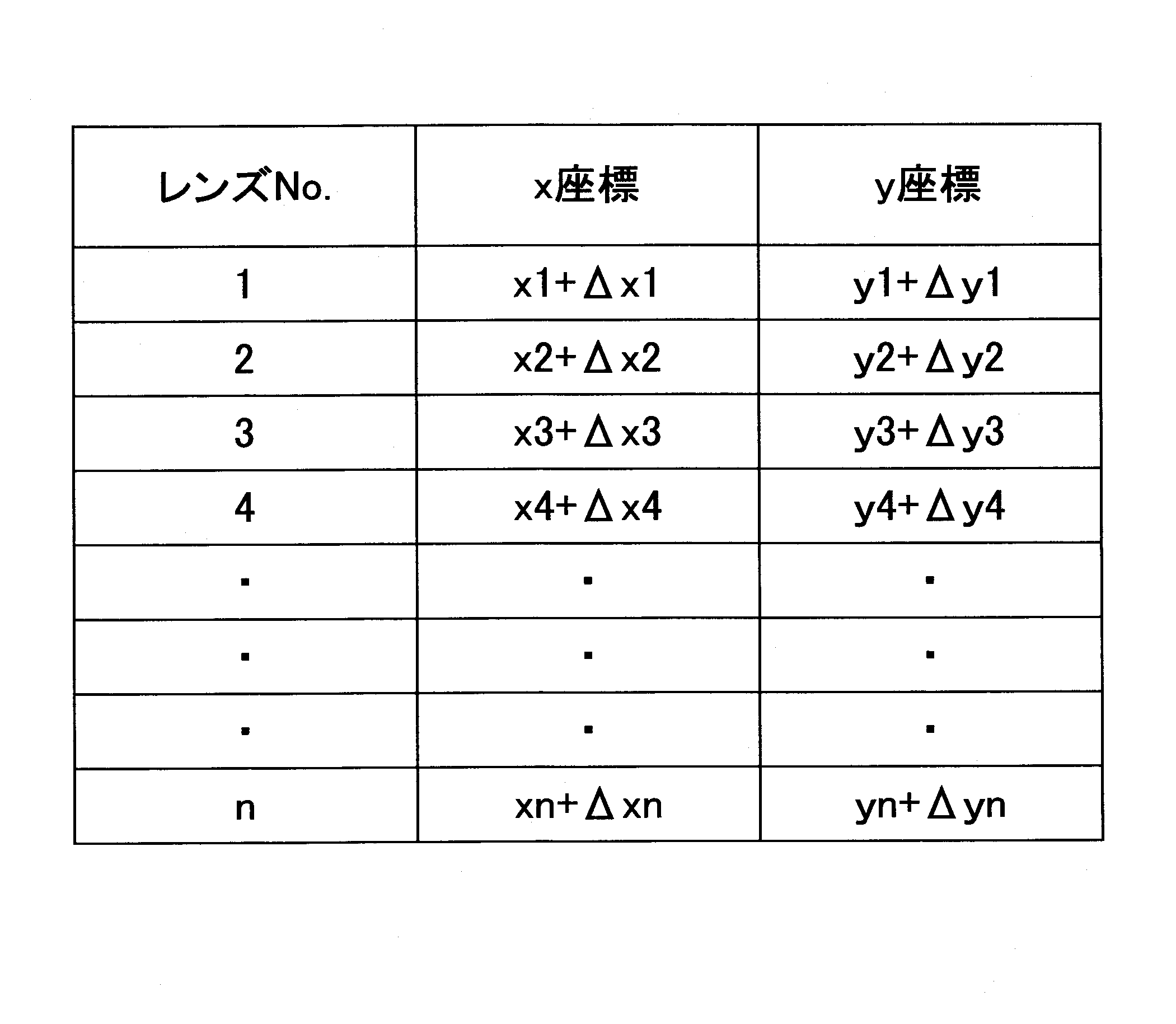
偏差量の分布を均等とすることにより、各マイクロレンズ50mのサイズの平均は、基準距離Rx、基準距離Ryと略等しくなる。そのため、スクリーン50の拡散角を、基準距離Rx、基準距離Ryで大きさが決まるレンズの開口数NA(Numerical Aperture)で求めることができる。
なお、発明者らの検討により、偏差量は、基準距離Rx、基準距離Ryに対して30%以下とすることが望ましい。つまり、Δx/Rx≦30%、Δy/Ry≦30%とすることが望ましい。これにより、スペックル低減機能を保持しつつ、干渉模様を低減することが可能となる。
なお、図5~図7を参照して、マイクロレンズの平面形状が四角形である場合(升目状に配置された四角配列の場合)について説明したが、これには限定されない。例えば、マイクロレンズの平面形状は六角形(蜂の巣状に配置された三角配列)であってもよいし、これら以外の平面形状であってもよい。
マイクロレンズ500mの平面形状が六角形の場合を図9~図10に示す。図9は、比較例に係るマイクロレンズアレイ(従来のマイクロレンズアレイ)を例示する図(その2)であり、図9(a)は斜視図、図9(b)は各マイクロレンズの中心位置を模式的に示した平面図である。又、図10は、本実施の形態に係るマイクロレンズアレイを例示する図(その2)であり、図10(a)は斜視図、図10(b)は各マイクロレンズの中心位置を模式的に示した平面図である。図11は、基準距離について説明する図(その2)であり、マイクロレンズアレイを模式的に例示する平面図である。
マイクロレンズ500mの平面形状が六角形の場合にも、マイクロレンズ500mの平面形状が四角形である場合と同様の手法により、各マイクロレンズ50mの中心50cをX方向及びY方向にランダム性を持って配置することができる。偏差量の分布を正規分布若しくは一様分布等とすることが望ましい点、及び、偏差量を基準距離Rx、基準距離Ryに対して30%以下とすることが望ましい点(つまり、Δx/Rx≦30%、Δy/Ry≦30%とすることが望ましい点)についても同様である。
このように、スクリーン50をマイクロレンズアレイ50mにより構成し、各マイクロレンズ50mの中心50cをX方向及びY方向にランダム性を持って配置することにより、スペックル低減機能を保持しつつ、干渉模様を低減することが可能となる。但し、各マイクロレンズ50mの中心50cをX方向、Y方向の何れか1方向のみにおいてランダム性を持って配置しても、スペックル低減機能を保持しつつ、干渉模様を低減することが可能となる。
なお、スクリーン50に照射した光ビームのスポット径(FWHM:半値幅)は、基準距離Rx、基準距離Ryよりも小さいことが望ましい。スクリーン50に照射した光ビームのスポット径が基準距離Rx、基準距離Ryよりも大きいと、光ビームが複数のマイクロレンズ50mに跨って照射される確率が高まり、干渉模様が発生し易くなるからである。
尚、上述の実施形態は本発明の好適な実施の例ではあるがこれに限定されるものではなく、本発明の要旨を逸脱しない範囲において種々変形実施可能である。
例えば、上記の実施の形態では、本発明に係る光走査制御装置をレーザ走査型プロジェクタに適用する例を示した。しかし、本発明に係る光走査制御装置は、上記の一例に限られない。本発明に係る光走査制御装置は、スクリーンに画像を表示する様々な機器に適用可能である。このような機器としては、例えば、車載用のヘッドアップディスプレイ、レーザプリンタ、レーザ走査型脱毛器、レーザヘッドランプ、レーザーレーダ等を挙げることができる。
なお、本発明に係る光走査制御装置のスクリーンを中間スクリーンとし、映像を間接的にフロントガラスやコンバイナに映すことで、スペックルノイズと干渉模様を低減した車載用のヘッドアップディスプレイが構築できる。
又、上記の実施の形態では、3つのレーザを有する例を示したが、レーザは最低1つ有していればよい。この場合、単色の光走査制御装置を実現できる。
本国際出願は2015年5月29日に出願された日本国特許出願第2015-109504号に基づく優先権を主張するものであり、日本国特許出願第2015-109504号の全内容を本国際出願に援用する。
1 光走査制御装置
10 回路部
11 システムコントローラ
12 CPU
13 バッファ回路
14 ミラー駆動回路
15 レーザ駆動回路
16 温度制御回路
20 光源部
21 LDモジュール
22 温度制御部
23 温度センサ
24 減光フィルタ
30 光走査部
40 光学部
41、42、43 反射ミラー
44 凹面ミラー
50 スクリーン
50m マイクロレンズ
50c マイクロレンズの中心
60 光量検出センサ
100 筐体
150 ユニット
211R、211G、211B レーザ
215 光量検出センサ
310 ミラー
351、352、371、372 駆動梁
391 水平変位センサ
395、396 垂直変位センサ
10 回路部
11 システムコントローラ
12 CPU
13 バッファ回路
14 ミラー駆動回路
15 レーザ駆動回路
16 温度制御回路
20 光源部
21 LDモジュール
22 温度制御部
23 温度センサ
24 減光フィルタ
30 光走査部
40 光学部
41、42、43 反射ミラー
44 凹面ミラー
50 スクリーン
50m マイクロレンズ
50c マイクロレンズの中心
60 光量検出センサ
100 筐体
150 ユニット
211R、211G、211B レーザ
215 光量検出センサ
310 ミラー
351、352、371、372 駆動梁
391 水平変位センサ
395、396 垂直変位センサ
Claims (5)
- レーザから出射された光を走査する走査手段と、
前記走査手段により走査された光が結像するスクリーンと、を有し、
前記スクリーンの光の入射側若しくは出射側の少なくとも一方の面に複数のマイクロレンズが配列され、
夫々の前記マイクロレンズは、第1の方向、前記第1の方向と直交する第2の方向の少なくとも1方向において、中心間距離をランダムにして配列されている光走査制御装置。 - 夫々の前記マイクロレンズが等間隔で配置された場合の中心間距離を基準距離としたときに、前記基準距離に対する夫々の前記マイクロレンズの中心間距離の偏差量の正負の分布割合が均等である請求項1記載の光走査制御装置。
- 夫々の前記マイクロレンズが等間隔で配置された場合の中心間距離を基準距離としたときに、前記スクリーンに照射されるレーザのスポット径は、前記基準距離よりも小さい請求項1記載の光走査制御装置。
- 夫々の前記マイクロレンズは、厚み及び曲率半径が統一されている請求項1記載の光走査制御装置。
- 夫々の前記マイクロレンズは、前記スクリーンの光の入射側の面に配列されている請求項1記載の光走査制御装置。
Priority Applications (3)
| Application Number | Priority Date | Filing Date | Title |
|---|---|---|---|
| CN201680026023.7A CN107533239B (zh) | 2015-05-29 | 2016-04-22 | 光扫描控制装置 |
| US15/572,227 US10571685B2 (en) | 2015-05-29 | 2016-04-22 | Optical scanning control device |
| EP16802952.8A EP3282302A4 (en) | 2015-05-29 | 2016-04-22 | Optical scanning control device |
Applications Claiming Priority (2)
| Application Number | Priority Date | Filing Date | Title |
|---|---|---|---|
| JP2015-109504 | 2015-05-29 | ||
| JP2015109504A JP6813769B2 (ja) | 2015-05-29 | 2015-05-29 | 光走査制御装置 |
Publications (1)
| Publication Number | Publication Date |
|---|---|
| WO2016194515A1 true WO2016194515A1 (ja) | 2016-12-08 |
Family
ID=57441051
Family Applications (1)
| Application Number | Title | Priority Date | Filing Date |
|---|---|---|---|
| PCT/JP2016/062824 Ceased WO2016194515A1 (ja) | 2015-05-29 | 2016-04-22 | 光走査制御装置 |
Country Status (5)
| Country | Link |
|---|---|
| US (1) | US10571685B2 (ja) |
| EP (1) | EP3282302A4 (ja) |
| JP (1) | JP6813769B2 (ja) |
| CN (1) | CN107533239B (ja) |
| WO (1) | WO2016194515A1 (ja) |
Families Citing this family (14)
| Publication number | Priority date | Publication date | Assignee | Title |
|---|---|---|---|---|
| DE102018120725A1 (de) * | 2018-08-24 | 2020-02-27 | Sick Ag | Optisches Strahlformungselement, Lichtsenderanordnung und optoelektronische Sensoranordnung |
| CN110850599A (zh) * | 2019-08-19 | 2020-02-28 | 上海鲲游光电科技有限公司 | 红外泛光照明组件 |
| JP7705235B2 (ja) * | 2019-10-25 | 2025-07-09 | デクセリアルズ株式会社 | 拡散板、表示装置、投影装置及び照明装置 |
| GB2588610A (en) * | 2019-10-28 | 2021-05-05 | Bae Systems Plc | Diffuser screens for head-up displays |
| EP3816678A1 (en) * | 2019-10-28 | 2021-05-05 | BAE SYSTEMS plc | Diffuser screens for head-up displays |
| JP2021081568A (ja) * | 2019-11-19 | 2021-05-27 | 株式会社リコー | 光学素子、表示装置、表示システムおよび移動体 |
| JP7369210B2 (ja) * | 2019-12-24 | 2023-10-25 | シチズン電子株式会社 | マイクロレンズアレイ及び発光装置 |
| US11892154B2 (en) * | 2020-07-08 | 2024-02-06 | Nippon Sheet Glass Company, Limited | Illumination device |
| CN114904151A (zh) * | 2020-07-31 | 2022-08-16 | 西安炬光科技股份有限公司 | 一种激光点阵系统及激光点阵治疗仪 |
| KR102439662B1 (ko) * | 2020-08-11 | 2022-09-05 | 주식회사 나무가 | 무작위 패턴을 가지는 마이크로 렌즈 어레이 및 그 제조방법 |
| JP7779854B2 (ja) | 2020-11-17 | 2025-12-03 | 株式会社クラレ | マイクロアレイ型拡散板 |
| CN112904660A (zh) * | 2021-02-01 | 2021-06-04 | 四川长虹电器股份有限公司 | 一种高增益宽视角超短焦激光投影屏结构 |
| JP2023119945A (ja) * | 2022-02-17 | 2023-08-29 | 株式会社ダイセル | マイクロレンズアレイ、拡散板及び照明装置 |
| DE102022210445A1 (de) | 2022-09-30 | 2024-04-04 | Continental Automotive Technologies GmbH | Anzeigeeinrichtung mit Diffusor |
Citations (6)
| Publication number | Priority date | Publication date | Assignee | Title |
|---|---|---|---|---|
| JP2008546002A (ja) * | 2005-05-17 | 2008-12-18 | シンボル テクノロジーズ, インコーポレイテッド | スペックルノイズを低減した画像投影スクリーン |
| JP2015057765A (ja) * | 2013-08-12 | 2015-03-26 | 大日本印刷株式会社 | 照明装置、投射装置、レンズアレイおよび光学モジュール |
| JP2015060092A (ja) * | 2013-09-19 | 2015-03-30 | ウシオ電機株式会社 | 光源装置およびプロジェクタ |
| JP2015169804A (ja) * | 2014-03-07 | 2015-09-28 | 株式会社リコー | レンズアレイ、画像表示装置、及び移動体 |
| WO2016035607A1 (ja) * | 2014-09-03 | 2016-03-10 | 三菱電機株式会社 | 画像表示装置 |
| WO2016052359A1 (ja) * | 2014-09-30 | 2016-04-07 | 旭硝子株式会社 | 画像光投影用スクリーンおよび表示システム |
Family Cites Families (8)
| Publication number | Priority date | Publication date | Assignee | Title |
|---|---|---|---|---|
| US6859326B2 (en) * | 2002-09-20 | 2005-02-22 | Corning Incorporated | Random microlens array for optical beam shaping and homogenization |
| JP4114656B2 (ja) * | 2004-10-20 | 2008-07-09 | セイコーエプソン株式会社 | レンズ基板、レンズ基板の製造方法、透過型スクリーンおよびリア型プロジェクタ |
| JP5075595B2 (ja) * | 2007-11-26 | 2012-11-21 | 株式会社東芝 | 表示装置及びそれを用いた移動体 |
| CN101850680B (zh) * | 2010-05-24 | 2012-06-06 | 苏州苏大维格光电科技股份有限公司 | 一种具有动态立体效果的安全薄膜 |
| JP5112556B2 (ja) | 2011-12-21 | 2013-01-09 | パイオニア株式会社 | 光源ユニット及びヘッドアップディスプレイ |
| KR101781206B1 (ko) * | 2011-12-30 | 2017-09-25 | 에스케이씨하이테크앤마케팅(유) | 마이크로 렌즈 광학시트, 및 이를 이용한 백라이트 유닛 및 액정 표시 장치 |
| JP6102194B2 (ja) * | 2012-11-09 | 2017-03-29 | 船井電機株式会社 | プロジェクタおよび投影用スクリーン |
| JP2015025977A (ja) * | 2013-07-26 | 2015-02-05 | 日本精機株式会社 | 走査型投影装置 |
-
2015
- 2015-05-29 JP JP2015109504A patent/JP6813769B2/ja active Active
-
2016
- 2016-04-22 WO PCT/JP2016/062824 patent/WO2016194515A1/ja not_active Ceased
- 2016-04-22 EP EP16802952.8A patent/EP3282302A4/en not_active Withdrawn
- 2016-04-22 US US15/572,227 patent/US10571685B2/en active Active
- 2016-04-22 CN CN201680026023.7A patent/CN107533239B/zh active Active
Patent Citations (6)
| Publication number | Priority date | Publication date | Assignee | Title |
|---|---|---|---|---|
| JP2008546002A (ja) * | 2005-05-17 | 2008-12-18 | シンボル テクノロジーズ, インコーポレイテッド | スペックルノイズを低減した画像投影スクリーン |
| JP2015057765A (ja) * | 2013-08-12 | 2015-03-26 | 大日本印刷株式会社 | 照明装置、投射装置、レンズアレイおよび光学モジュール |
| JP2015060092A (ja) * | 2013-09-19 | 2015-03-30 | ウシオ電機株式会社 | 光源装置およびプロジェクタ |
| JP2015169804A (ja) * | 2014-03-07 | 2015-09-28 | 株式会社リコー | レンズアレイ、画像表示装置、及び移動体 |
| WO2016035607A1 (ja) * | 2014-09-03 | 2016-03-10 | 三菱電機株式会社 | 画像表示装置 |
| WO2016052359A1 (ja) * | 2014-09-30 | 2016-04-07 | 旭硝子株式会社 | 画像光投影用スクリーンおよび表示システム |
Non-Patent Citations (1)
| Title |
|---|
| See also references of EP3282302A4 * |
Also Published As
| Publication number | Publication date |
|---|---|
| JP6813769B2 (ja) | 2021-01-13 |
| EP3282302A4 (en) | 2019-01-02 |
| EP3282302A1 (en) | 2018-02-14 |
| CN107533239A (zh) | 2018-01-02 |
| US20180149860A1 (en) | 2018-05-31 |
| JP2016224212A (ja) | 2016-12-28 |
| US10571685B2 (en) | 2020-02-25 |
| CN107533239B (zh) | 2020-05-08 |
Similar Documents
| Publication | Publication Date | Title |
|---|---|---|
| JP6813769B2 (ja) | 光走査制御装置 | |
| JP6340807B2 (ja) | 画像表示装置及び移動体 | |
| JP6409511B2 (ja) | ヘッドアップディスプレイ装置 | |
| EP1411379B1 (en) | Modulated light source using a vertical cavity surface emitting laser (VCSEL) array with an electromechanical grating device | |
| KR101771912B1 (ko) | 화상 프로젝터 및 광학 조립체 | |
| WO2017098913A1 (ja) | 光走査装置、画像表示装置、および車両 | |
| US20180374407A1 (en) | Image display device | |
| KR20200016210A (ko) | 주사형 표시 장치 및 주사형 표시 시스템 | |
| US20200226963A1 (en) | Optical scanner, display system, mobile object, optical scanning control method, and recording medium storing program code | |
| JP2015225216A (ja) | 画像表示装置 | |
| JP6402854B2 (ja) | 透過型スクリーン及びそれを用いたヘッドアップディスプレイ装置 | |
| WO2016006151A1 (ja) | 画像表示装置 | |
| JP2021135472A (ja) | 表示装置、及び移動体 | |
| US10598830B2 (en) | Screen member, image display apparatus, and object apparatus | |
| CN112567286B (zh) | 具有增加的均匀性的扫描显示器 | |
| JP2015225218A (ja) | 画像表示装置 | |
| WO2016194513A1 (ja) | 光走査制御装置 | |
| JP2014240958A (ja) | 光モジュール | |
| JP6457164B1 (ja) | 走査型表示装置、走査型表示システム、及び光拡散部の製造方法 | |
| JP6813785B2 (ja) | 光走査制御装置 | |
| JP6624275B2 (ja) | 画像表示装置 | |
| JP6651139B2 (ja) | 画像表示装置及び移動体 | |
| JP6608557B2 (ja) | 走査型表示装置及び走査型表示システム | |
| JP2024092971A (ja) | 光源ユニットおよび映像表示装置 | |
| JP2021081568A (ja) | 光学素子、表示装置、表示システムおよび移動体 |
Legal Events
| Date | Code | Title | Description |
|---|---|---|---|
| 121 | Ep: the epo has been informed by wipo that ep was designated in this application |
Ref document number: 16802952 Country of ref document: EP Kind code of ref document: A1 |
|
| WWE | Wipo information: entry into national phase |
Ref document number: 15572227 Country of ref document: US |
|
| NENP | Non-entry into the national phase |
Ref country code: DE |