WO2016203887A1 - 新規な化合物、薄膜形成用原料及び薄膜の製造方法 - Google Patents
新規な化合物、薄膜形成用原料及び薄膜の製造方法 Download PDFInfo
- Publication number
- WO2016203887A1 WO2016203887A1 PCT/JP2016/064573 JP2016064573W WO2016203887A1 WO 2016203887 A1 WO2016203887 A1 WO 2016203887A1 JP 2016064573 W JP2016064573 W JP 2016064573W WO 2016203887 A1 WO2016203887 A1 WO 2016203887A1
- Authority
- WO
- WIPO (PCT)
- Prior art keywords
- thin film
- compound
- raw material
- temperature
- titanium
- Prior art date
- Legal status (The legal status is an assumption and is not a legal conclusion. Google has not performed a legal analysis and makes no representation as to the accuracy of the status listed.)
- Ceased
Links
- 0 *CC(C12)/*(/*)=C/C=*(\*)/C(C3)C13C21*(*)=CC=*1* Chemical compound *CC(C12)/*(/*)=C/C=*(\*)/C(C3)C13C21*(*)=CC=*1* 0.000 description 2
Images


Classifications
-
- C—CHEMISTRY; METALLURGY
- C23—COATING METALLIC MATERIAL; COATING MATERIAL WITH METALLIC MATERIAL; CHEMICAL SURFACE TREATMENT; DIFFUSION TREATMENT OF METALLIC MATERIAL; COATING BY VACUUM EVAPORATION, BY SPUTTERING, BY ION IMPLANTATION OR BY CHEMICAL VAPOUR DEPOSITION, IN GENERAL; INHIBITING CORROSION OF METALLIC MATERIAL OR INCRUSTATION IN GENERAL
- C23C—COATING METALLIC MATERIAL; COATING MATERIAL WITH METALLIC MATERIAL; SURFACE TREATMENT OF METALLIC MATERIAL BY DIFFUSION INTO THE SURFACE, BY CHEMICAL CONVERSION OR SUBSTITUTION; COATING BY VACUUM EVAPORATION, BY SPUTTERING, BY ION IMPLANTATION OR BY CHEMICAL VAPOUR DEPOSITION, IN GENERAL
- C23C16/00—Chemical coating by decomposition of gaseous compounds, without leaving reaction products of surface material in the coating, i.e. chemical vapour deposition [CVD] processes
- C23C16/06—Chemical coating by decomposition of gaseous compounds, without leaving reaction products of surface material in the coating, i.e. chemical vapour deposition [CVD] processes characterised by the deposition of metallic material
- C23C16/18—Chemical coating by decomposition of gaseous compounds, without leaving reaction products of surface material in the coating, i.e. chemical vapour deposition [CVD] processes characterised by the deposition of metallic material from metallo-organic compounds
-
- C—CHEMISTRY; METALLURGY
- C07—ORGANIC CHEMISTRY
- C07F—ACYCLIC, CARBOCYCLIC OR HETEROCYCLIC COMPOUNDS CONTAINING ELEMENTS OTHER THAN CARBON, HYDROGEN, HALOGEN, OXYGEN, NITROGEN, SULFUR, SELENIUM OR TELLURIUM
- C07F13/00—Compounds containing elements of Groups 7 or 17 of the Periodic Table
-
- C—CHEMISTRY; METALLURGY
- C07—ORGANIC CHEMISTRY
- C07F—ACYCLIC, CARBOCYCLIC OR HETEROCYCLIC COMPOUNDS CONTAINING ELEMENTS OTHER THAN CARBON, HYDROGEN, HALOGEN, OXYGEN, NITROGEN, SULFUR, SELENIUM OR TELLURIUM
- C07F13/00—Compounds containing elements of Groups 7 or 17 of the Periodic Table
- C07F13/005—Compounds without a metal-carbon linkage
-
- C—CHEMISTRY; METALLURGY
- C07—ORGANIC CHEMISTRY
- C07F—ACYCLIC, CARBOCYCLIC OR HETEROCYCLIC COMPOUNDS CONTAINING ELEMENTS OTHER THAN CARBON, HYDROGEN, HALOGEN, OXYGEN, NITROGEN, SULFUR, SELENIUM OR TELLURIUM
- C07F15/00—Compounds containing elements of Groups 8, 9, 10 or 18 of the Periodic Table
- C07F15/04—Nickel compounds
- C07F15/045—Nickel compounds without a metal-carbon linkage
-
- C—CHEMISTRY; METALLURGY
- C07—ORGANIC CHEMISTRY
- C07F—ACYCLIC, CARBOCYCLIC OR HETEROCYCLIC COMPOUNDS CONTAINING ELEMENTS OTHER THAN CARBON, HYDROGEN, HALOGEN, OXYGEN, NITROGEN, SULFUR, SELENIUM OR TELLURIUM
- C07F15/00—Compounds containing elements of Groups 8, 9, 10 or 18 of the Periodic Table
- C07F15/06—Cobalt compounds
- C07F15/065—Cobalt compounds without a metal-carbon linkage
-
- C—CHEMISTRY; METALLURGY
- C23—COATING METALLIC MATERIAL; COATING MATERIAL WITH METALLIC MATERIAL; CHEMICAL SURFACE TREATMENT; DIFFUSION TREATMENT OF METALLIC MATERIAL; COATING BY VACUUM EVAPORATION, BY SPUTTERING, BY ION IMPLANTATION OR BY CHEMICAL VAPOUR DEPOSITION, IN GENERAL; INHIBITING CORROSION OF METALLIC MATERIAL OR INCRUSTATION IN GENERAL
- C23C—COATING METALLIC MATERIAL; COATING MATERIAL WITH METALLIC MATERIAL; SURFACE TREATMENT OF METALLIC MATERIAL BY DIFFUSION INTO THE SURFACE, BY CHEMICAL CONVERSION OR SUBSTITUTION; COATING BY VACUUM EVAPORATION, BY SPUTTERING, BY ION IMPLANTATION OR BY CHEMICAL VAPOUR DEPOSITION, IN GENERAL
- C23C16/00—Chemical coating by decomposition of gaseous compounds, without leaving reaction products of surface material in the coating, i.e. chemical vapour deposition [CVD] processes
- C23C16/44—Chemical coating by decomposition of gaseous compounds, without leaving reaction products of surface material in the coating, i.e. chemical vapour deposition [CVD] processes characterised by the method of coating
- C23C16/448—Chemical coating by decomposition of gaseous compounds, without leaving reaction products of surface material in the coating, i.e. chemical vapour deposition [CVD] processes characterised by the method of coating characterised by the method used for generating reactive gas streams, e.g. by evaporation or sublimation of precursor materials
- C23C16/4481—Chemical coating by decomposition of gaseous compounds, without leaving reaction products of surface material in the coating, i.e. chemical vapour deposition [CVD] processes characterised by the method of coating characterised by the method used for generating reactive gas streams, e.g. by evaporation or sublimation of precursor materials by evaporation using carrier gas in contact with the source material
-
- C—CHEMISTRY; METALLURGY
- C23—COATING METALLIC MATERIAL; COATING MATERIAL WITH METALLIC MATERIAL; CHEMICAL SURFACE TREATMENT; DIFFUSION TREATMENT OF METALLIC MATERIAL; COATING BY VACUUM EVAPORATION, BY SPUTTERING, BY ION IMPLANTATION OR BY CHEMICAL VAPOUR DEPOSITION, IN GENERAL; INHIBITING CORROSION OF METALLIC MATERIAL OR INCRUSTATION IN GENERAL
- C23C—COATING METALLIC MATERIAL; COATING MATERIAL WITH METALLIC MATERIAL; SURFACE TREATMENT OF METALLIC MATERIAL BY DIFFUSION INTO THE SURFACE, BY CHEMICAL CONVERSION OR SUBSTITUTION; COATING BY VACUUM EVAPORATION, BY SPUTTERING, BY ION IMPLANTATION OR BY CHEMICAL VAPOUR DEPOSITION, IN GENERAL
- C23C16/00—Chemical coating by decomposition of gaseous compounds, without leaving reaction products of surface material in the coating, i.e. chemical vapour deposition [CVD] processes
- C23C16/44—Chemical coating by decomposition of gaseous compounds, without leaving reaction products of surface material in the coating, i.e. chemical vapour deposition [CVD] processes characterised by the method of coating
- C23C16/455—Chemical coating by decomposition of gaseous compounds, without leaving reaction products of surface material in the coating, i.e. chemical vapour deposition [CVD] processes characterised by the method of coating characterised by the method used for introducing gases into reaction chamber or for modifying gas flows in reaction chamber
- C23C16/45523—Pulsed gas flow or change of composition over time
- C23C16/45525—Atomic layer deposition [ALD]
- C23C16/45553—Atomic layer deposition [ALD] characterized by the use of precursors specially adapted for ALD
-
- H—ELECTRICITY
- H10—SEMICONDUCTOR DEVICES; ELECTRIC SOLID-STATE DEVICES NOT OTHERWISE PROVIDED FOR
- H10P—GENERIC PROCESSES OR APPARATUS FOR THE MANUFACTURE OR TREATMENT OF DEVICES COVERED BY CLASS H10
- H10P14/00—Formation of materials, e.g. in the shape of layers or pillars
- H10P14/40—Formation of materials, e.g. in the shape of layers or pillars of conductive or resistive materials
- H10P14/42—Formation of materials, e.g. in the shape of layers or pillars of conductive or resistive materials using a gas or vapour
Definitions
- the present invention relates to a novel compound, a raw material for forming a thin film containing the compound, and a method for producing a thin film using the raw material for forming a thin film, and more specifically, a novel compound comprising a diazadiene metal compound,
- the present invention relates to a thin film forming raw material containing a compound and a method for producing a thin film using the thin film forming raw material.
- Thin film materials containing metal elements are applied to various applications because they exhibit electrical characteristics and optical characteristics.
- copper and copper-containing thin films are applied as LSI wiring materials because of their high conductivity, high electromigration resistance, and high melting point.
- Nickel and nickel-containing thin films are mainly used for members of electronic parts such as resistance films and barrier films, members for recording media such as magnetic films, and members for thin film solar cells such as electrodes.
- Cobalt and cobalt-containing thin films are used for electrode films, resistance films, adhesive films, magnetic tapes, carbide tool members, and the like.
- Examples of the method for producing the thin film include a sputtering method, an ion plating method, a MOD method such as a coating pyrolysis method and a sol-gel method, a chemical vapor deposition method, etc., but has excellent composition controllability and step coverage. Since it has many advantages such as being suitable for mass production and being capable of hybrid integration, chemical vapor deposition including ALD (Atomic Layer Deposition) method (hereinafter simply referred to as “CVD”) ) Method is the optimal manufacturing process.
- ALD Atomic Layer Deposition
- Patent Document 1 discloses a diazadienyl complex that can be used as a raw material for forming a thin film by an ALD method.
- Patent Document 2 discloses a diazadiene metal compound that can be used in chemical vapor deposition or atomic layer deposition.
- Patent Document 1 and Patent Document 2 do not describe any novel compounds composed of the diazadiene metal compound of the present invention.
- an object of the present invention is to form a high-quality metal with a low vapor pressure, a low melting point, and a low energy when forming a thin film containing a metal on the substrate surface by vaporizing a chemical vapor deposition raw material or the like.
- a novel compound comprising a diazadiene-based metal compound for use in a thin film-forming material capable of producing a thin film, a raw material for forming a thin film containing the compound, and production of a thin film using the raw material for forming a thin film It is to provide a method.
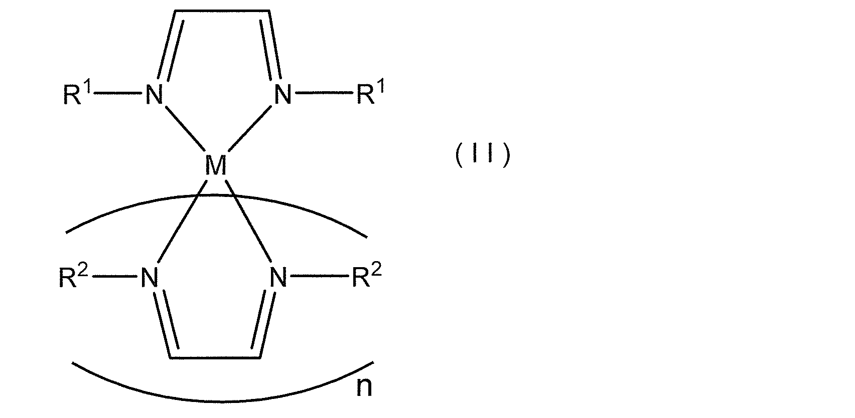
- the present invention provides a novel compound represented by the following general formula (I) or the following general formula (II), a raw material for forming a thin film containing the compound, and a method for producing a thin film using the raw material Is:
- R 1 and R 2 each independently represents a hydrocarbon group having 1 to 12 carbon atoms, and the hydrogen atom of the hydrocarbon group may be substituted with Si (R 3 ) 3 .
- R 1 and R 2 are different groups.
- R 3 represents a methyl group or an ethyl group
- M represents a metal atom or a silicon atom
- n represents an integer of 1 to 4.
- R 1, R 2, R 3, M and n have the same meanings as in formula (I). ]
- the present invention it is possible to obtain a low melting point compound which has a high vapor pressure, a low thermal decomposition temperature, and becomes liquid at normal pressure of 30 ° C. or slight heating.
- the compound is particularly suitable as a thin film forming raw material for forming a metal thin film by a CVD method, and can be preferably used as a thin film forming raw material for forming a metal thin film by an ALD method.
- the compound of the present invention is represented by the above general formula (I) or the above general formula (II), and is suitable as a precursor for a thin film production method having a vaporization step such as a CVD method. It can also be used to form a thin film.
- the compound of the present invention has a low melting point and is a compound which becomes liquid at normal pressure of 30 ° C. or becomes liquid by slight heating. Since a compound having a low melting point has good transportability, it is suitable as a precursor for a thin film production method having a vaporization step such as a CVD method. Furthermore, the compound of the present invention is a compound having a low thermal decomposition temperature. When a compound having a low thermal decomposition temperature is used as a precursor for a thin film production method having a vaporization step such as a CVD method, a thin film can be obtained with low energy.
- R 1 and R 2 each independently represent a hydrocarbon group having 1 to 10 carbon atoms, and the hydrogen atom of the hydrocarbon group is Si In some cases, (R 3 ) 3 may be substituted.
- R 1 and R 2 are different groups.
- R 3 represents a methyl group or an ethyl group
- M represents a metal atom or a silicon atom
- n represents an integer of 1 to 4.
- Examples of the hydrocarbon group having 1 to 12 carbon atoms represented by R 1 and R 2 include alkyl, alkenyl, cycloalkyl, aryl, cyclopentadienyl and the like.
- the hydrogen atom of these hydrocarbon groups may be substituted with Si (R 3 ) 3 .
- Si (R 3 ) 3 represents a trimethylsilyl group or a triethylsilyl group, and one hydrogen atom substituted with Si (R 3 ) 3 is preferably one for one hydrocarbon group.
- alkyl examples include methyl, ethyl, propyl, isopropyl, butyl, isobutyl, sec-butyl, sec-butyl, pentyl, amyl, isoamyl, hexyl, heptyl, isoheptyl, octyl, isooctyl, 2-ethylhexyl, nonyl, isononyl , Decyl, dodecyl and the like.
- alkenyl examples include vinyl, 1-methylethenyl, 2-methylethenyl, propenyl, butenyl, isobutenyl, pentenyl, hexenyl, heptenyl, octenyl, decenyl and the like.
- cycloalkyl examples include cyclohexyl, cyclopentyl, cycloheptyl, methylcyclopentyl, methylcyclohexyl, methylcycloheptyl, cyclopentenyl, cyclohexenyl, cycloheptenyl, methylcyclopentenyl, methylcyclohexenyl, methylcycloheptenyl, and the like.
- aryl examples include phenyl, naphthyl, 2-methylphenyl, 3-methylphenyl, 4-methylphenyl, 4-vinylphenyl, 3-isopropylphenyl, 4-isopropylphenyl, 4-butylphenyl, and 4-isobutylphenyl. 4-tert-butylphenyl, 4-hexylphenyl, 4-cyclohexylphenyl and the like.
- cyclopentadienyl examples include cyclopentadienyl, methylcyclopentadienyl, ethylcyclopentadienyl, propylcyclopentadienyl, isopropylcyclopentadienyl, butylcyclopentadienyl, and secondary butylcyclopenta Examples include dienyl, isobutylcyclopentadienyl, tertiary butylcyclopentadienyl, dimethylcyclopentadienyl, tetramethylcyclopentadienyl, and the like.
- M represents a metal atom or a silicon atom.
- the metal atom is not particularly limited.
- n represents an integer of 1 to 4. Note that n is preferably 1.
- R 1 is a primary alkyl group having 1 to 5 carbon atoms
- R 2 is a secondary or tertiary alkyl group having 1 to 5 carbon atoms.
- the vapor pressure is high
- the melting point is low
- the thermal decomposition temperature is low.
- a compound in which R 1 and R 2 having 1 to 5 carbon atoms are secondary or tertiary alkyl groups has a high vapor pressure, a low thermal decomposition temperature
- R 1 is a primary alkyl group
- R 1 is a secondary alkyl group and R 2 is a tertiary alkyl group are particularly preferred because of their high vapor pressure and low thermal stability.
- a compound in which R 1 is an isopropyl group and R 2 is a tert-butyl group is particularly preferable because the above-described effect is particularly high and the compound does not deteriorate for more than 3 weeks even when left at normal pressure 120 ° C. .
- M is copper, iron, nickel, cobalt, or manganese
- n is particularly preferably 1 because the effects of high vapor pressure, low melting point, and low thermal decomposition temperature are particularly high.
- R 1 and R 2 can be arbitrarily selected depending on the solubility in the solvent used, the thin film formation reaction, and the like.
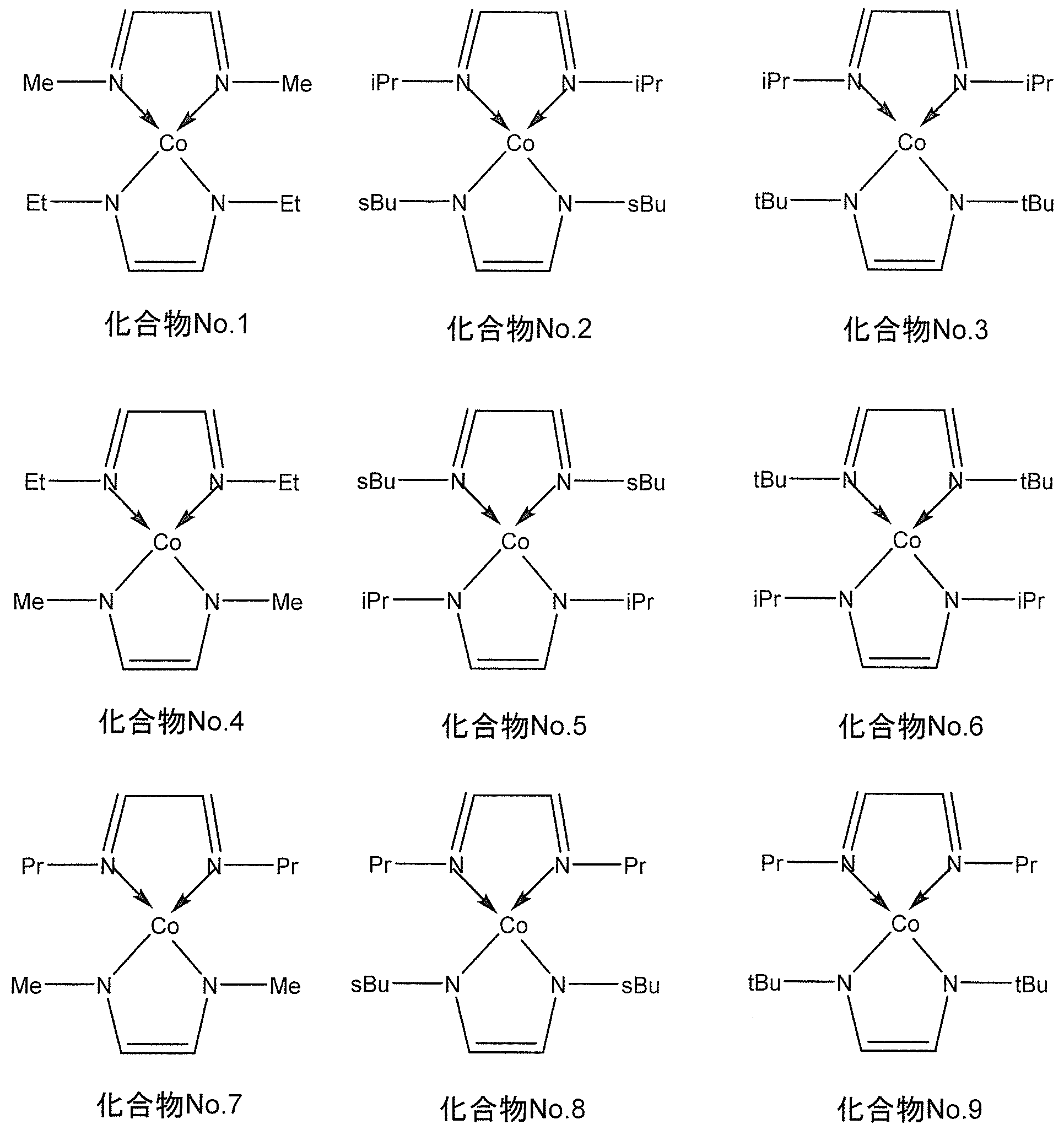
- the compound represented by the general formula (I) for example, when M is cobalt, the following chemical formula No. 1-No.
- the compound represented by 9 is mentioned.
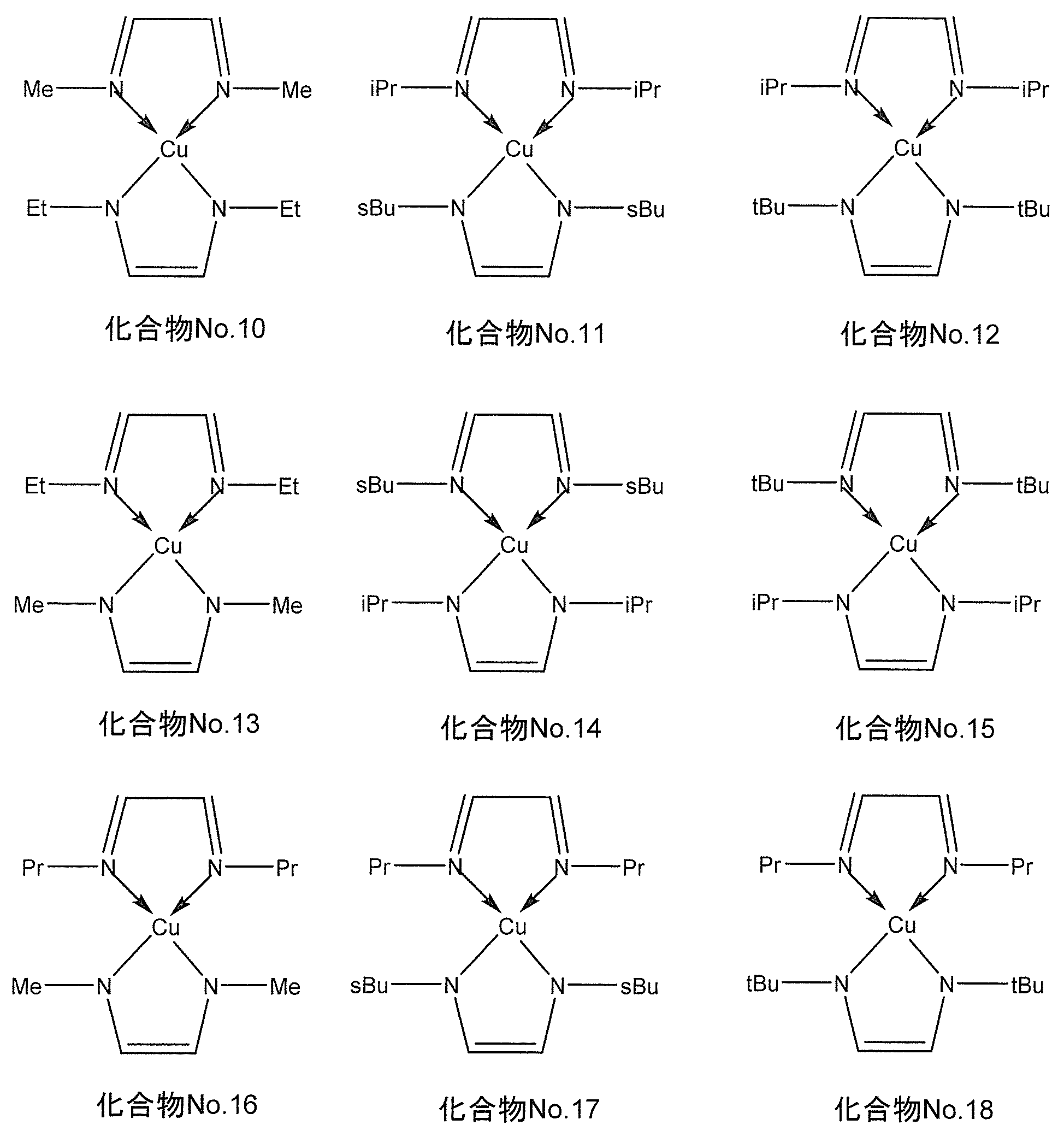
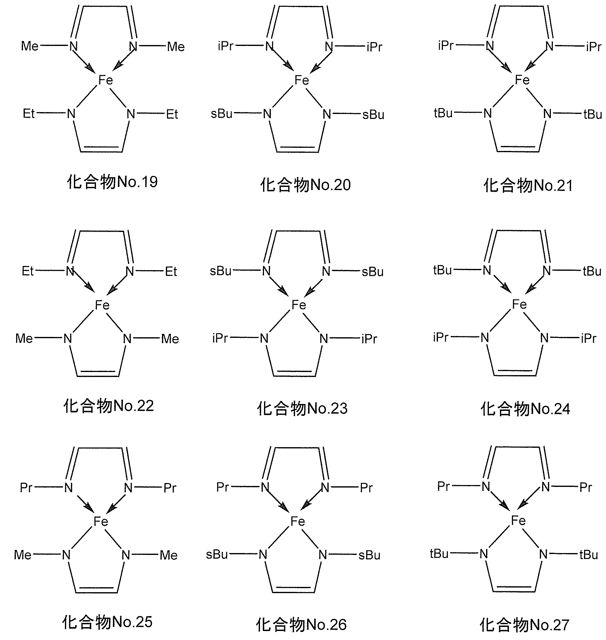
- the following chemical formula No. 1-No. 9 “Me” represents a methyl group, “Et” represents an ethyl group, “Pr” represents a propyl group, “iPr” represents isopropyl, “sbu” represents a secondary butyl group, “tBu” represents a tertiary butyl group.
- the compound represented by the general formula (I) for example, when M is copper, the following chemical formula No. 10-No.
- the compound represented by 18 is mentioned.
- the compound represented by the general formula (I) for example, when M is iron, the following chemical formula No. 19-No.
- the compound represented by 27 is mentioned.
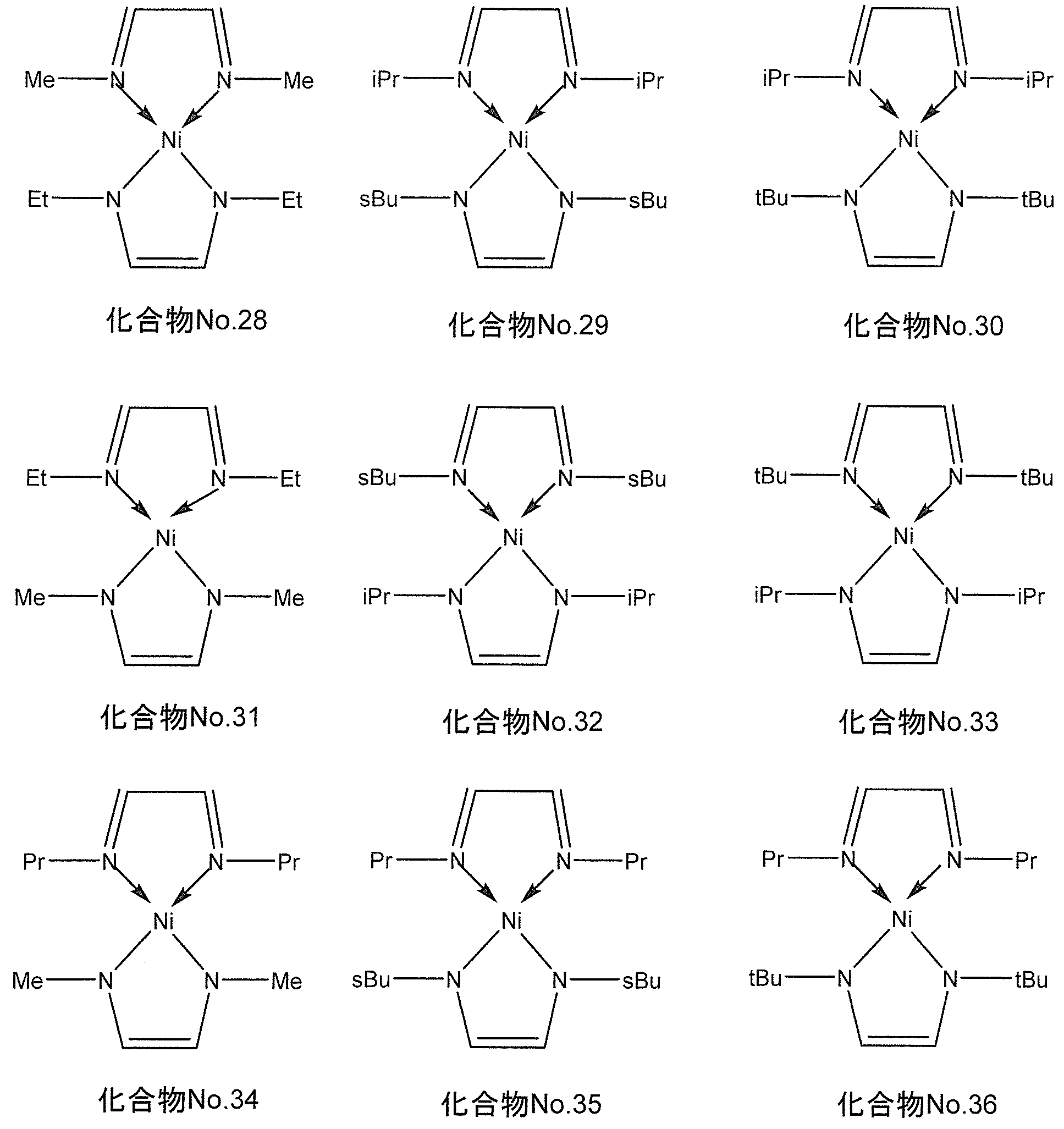
- the compound represented by the general formula (I) for example, when M is nickel, the following chemical formula No. 28-No. And a compound represented by 36.
- the following chemical formula No. 28-No. 36 “Me” represents a methyl group, “Et” represents an ethyl group, “Pr” represents a propyl group, “iPr” represents isopropyl, “sbu” represents a secondary butyl group, “ “tBu” represents a tertiary butyl group.
- the compound represented by the general formula (I) for example, when M is manganese, the following chemical formula No. 37-No. And a compound represented by 45.
- the following chemical formula No. 37-No. 45 “Me” represents a methyl group, “Et” represents an ethyl group, “Pr” represents a propyl group, “iPr” represents isopropyl, “sbu” represents a secondary butyl group, “tBu” represents a tertiary butyl group.
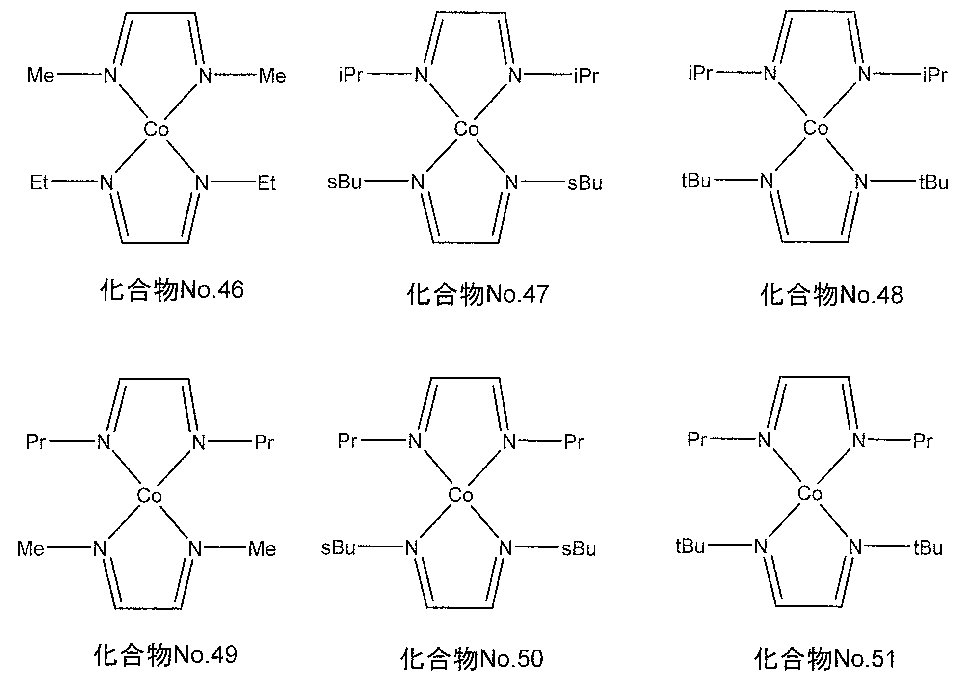
- the following chemical formula No. 46-No. A compound represented by 51 As a preferred specific example of the compound represented by the general formula (II), for example, when M is cobalt, the following chemical formula No. 46-No. A compound represented by 51.
- the following chemical formula No. 46-No. 51 “Me” represents a methyl group, “Et” represents an ethyl group, “Pr” represents a propyl group, “iPr” represents isopropyl, “sbu” represents a secondary butyl group, “tBu” represents a tertiary butyl group.
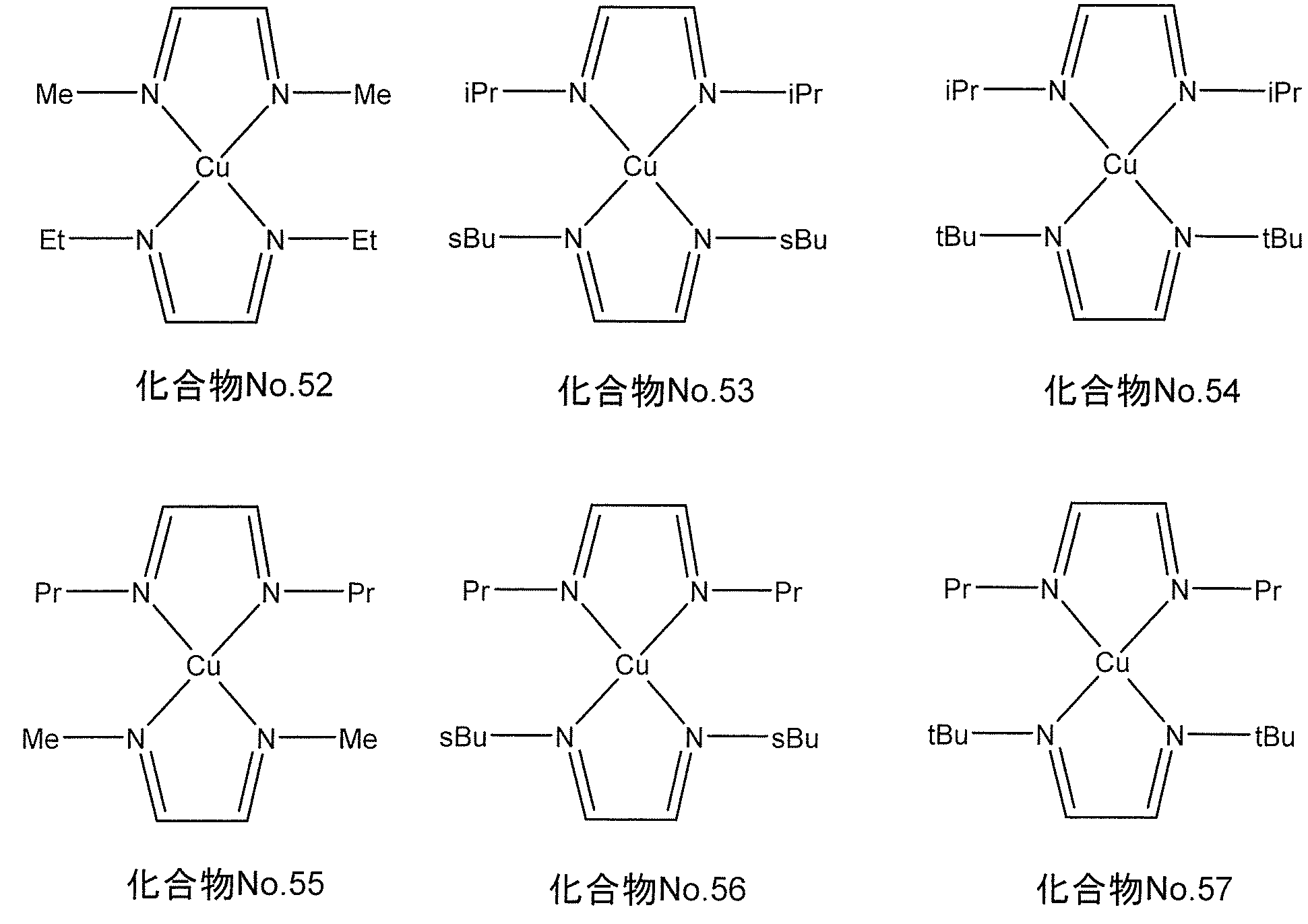
- the compound represented by the general formula (II) for example, when M is copper, the following chemical formula No. 52-No.
- the compound represented by 57 is mentioned.
- the following chemical formula No. 52-No. 57 “Me” represents a methyl group, “Et” represents an ethyl group, “Pr” represents a propyl group, “iPr” represents isopropyl, “sbu” represents a secondary butyl group, “tBu” represents a tertiary butyl group.
- the compound represented by the general formula (II) for example, when M is iron, the following chemical formula No. 58-No.
- the compound represented by 63 is mentioned.
- the following chemical formula No. 58-No. 63 “Me” represents a methyl group, “Et” represents an ethyl group, “Pr” represents a propyl group, “iPr” represents isopropyl, “sbu” represents a secondary butyl group, “tBu” represents a tertiary butyl group.
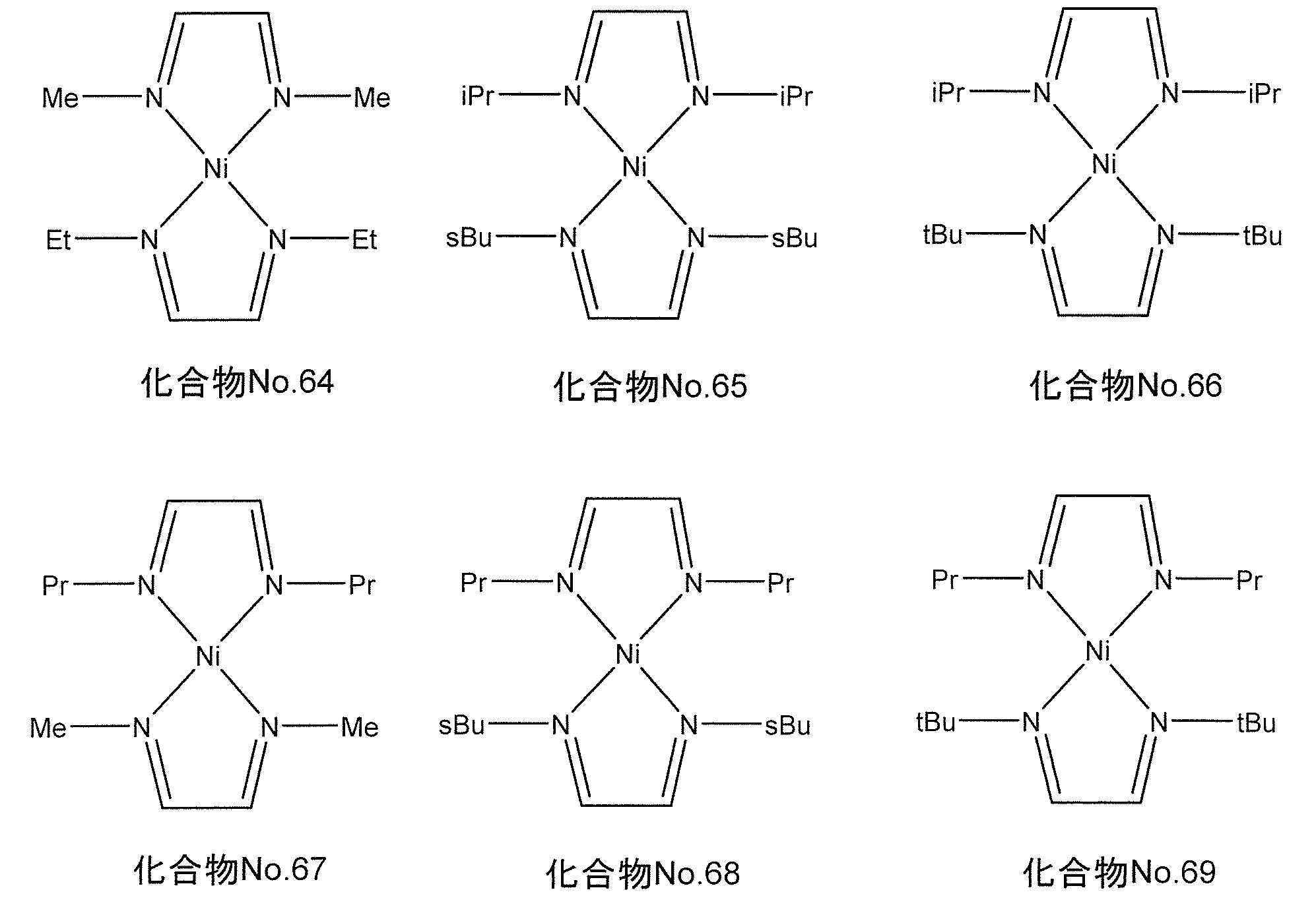
- the compound represented by the general formula (II) for example, when M is nickel, the following chemical formula No. 64-No.
- the compound represented by 69 is mentioned.
- the following chemical formula No. 64-No. 69 “Me” represents a methyl group, “Et” represents an ethyl group, “Pr” represents a propyl group, “iPr” represents isopropyl, “sbu” represents a secondary butyl group, “tBu” represents a tertiary butyl group.
- the compound represented by the general formula (II) for example, when M is manganese, the following chemical formula No. 70-No. And a compound represented by 75.
- the following chemical formula No. 70-No. 75 “Me” represents a methyl group, “Et” represents an ethyl group, “Pr” represents a propyl group, “iPr” represents isopropyl, “sbu” represents a secondary butyl group, “tBu” represents a tertiary butyl group.
- the compound of the present invention is not particularly limited by its production method, and can be produced by applying known reactions.
- an inorganic salt such as a halide of cobalt or nitrate or a hydrate thereof, and a corresponding diazadiene compound
- a method of reacting an inorganic salt such as a cobalt halide or nitrate or a hydrate thereof with a corresponding diazadiene compound can be used.
- an inorganic salt such as a cobalt halide or nitrate, or a hydrate thereof is applicable.
- a method of reacting a diazadiene compound in the presence of a base such as sodium, lithium, sodium hydride, sodium amide, sodium hydroxide, sodium methylate, ammonia or amine; an inorganic salt such as cobalt halide or nitrate or the like A method of reacting a hydrate with a sodium complex, lithium complex, potassium complex or the like of the corresponding diazadiene compound; disproportionation of the compound represented by the general formula (I) of the present invention can be used.
- the thin film forming raw material of the present invention is a thin film precursor obtained from the above-described compound of the present invention, and the form of the thin film forming raw material can be variously changed depending on the manufacturing process to which the thin film forming raw material is applied. Can do. For example, when a thin film containing only one kind of metal or silicon is produced, the raw material for forming a thin film of the present invention does not contain a metal compound and a semimetal compound other than the above compounds.
- the raw material for forming a thin film of the present invention includes a compound containing a desired metal and / or a compound containing a metalloid in addition to the above compound ( Hereinafter, it is also referred to as “another precursor”. Furthermore, the raw material for forming a thin film of the present invention may further contain an organic solvent and / or a nucleophilic reagent, as will be described later.
- the thin film forming raw material of the present invention is suitable for the chemical vapor deposition raw material (hereinafter referred to as “for CVD”) because the physical properties of the compound of the present invention that can be used as a precursor are suitable for the CVD method and the ALD method. It is also useful as a “raw material”).
- CVD chemical vapor deposition raw material
- the thin film forming raw material of the present invention is a chemical vapor deposition raw material
- the form of the thin film forming raw material can be appropriately selected by a method such as a transporting and supplying method of the CVD method used.
- a CVD raw material is vaporized by heating and / or reducing pressure in a container in which the raw material is stored (hereinafter sometimes simply referred to as a “raw material container”).
- a gas that introduces the vapor into a film forming chamber (hereinafter sometimes referred to as “deposition reaction part”) in which the substrate is installed, together with a carrier gas such as argon, nitrogen, and helium used as necessary.
- Transport method and liquid transport that transports the raw material for CVD to the vaporization chamber in a liquid or solution state, vaporizes it by heating and / or decompressing in the vaporization chamber, and introduces the vapor into the film forming chamber.
- the compound itself represented by the general formula (I) or the general formula (II) can be used as a raw material for CVD.
- the compound itself represented by the general formula (I) or the general formula (II) or a solution obtained by dissolving the compound in an organic solvent can be used as a raw material for CVD.
- These CVD raw materials may further contain other precursors, nucleophilic reagents, and the like.
- a CVD raw material is vaporized and supplied independently for each component (hereinafter sometimes referred to as a “single source method”), and a multi-component raw material with a desired composition in advance.
- a method of vaporizing and supplying the mixed raw material hereinafter, sometimes referred to as “cocktail sauce method”.
- a mixture of the compound of the present invention and another precursor or a mixed solution obtained by dissolving the mixture in an organic solvent can be used as a raw material for CVD.
- this mixture or mixed solution may further contain a nucleophilic reagent or the like.
- the above organic solvent is not particularly limited, and a known general organic solvent can be used.
- the organic solvent include acetates such as ethyl acetate, butyl acetate, and methoxyethyl acetate; ethers such as tetrahydrofuran, tetrahydropyran, ethylene glycol dimethyl ether, diethylene glycol dimethyl ether, triethylene glycol dimethyl ether, dibutyl ether, and dioxane; Ketones, methyl isobutyl ketone, ethyl butyl ketone, dipropyl ketone, diisobutyl ketone, methyl amyl ketone, cyclohexanone, methylcyclohexanone and other ketones; hexane, cyclohexane, methylcyclohexane, dimethylcyclohexane, ethylcyclohexane, heptane, octan
- the total amount of the precursor in the CVD raw material which is a solution in which the precursor is dissolved in the organic solvent, is 0.01 to 2.0 mol / liter, particularly 0.05 to 1.0 mol. / Liter is preferable.
- the amount of the precursor as a whole is the amount of the compound of the present invention when the thin film forming raw material of the present invention does not contain a metal compound and a metalloid compound other than the compound of the present invention.
- a compound containing another metal and / or a compound containing a metalloid is the total amount of the compound of the present invention and another precursor.
- Other precursors include hydrides, hydroxides, halides, azides, alkyls, alkenyls, cycloalkyls, aryls, alkynyls, aminos, dialkylaminoalkyls, monoalkylaminos, dialkylaminos, diamines, di (silyl-alkyls) ) Amino, di (alkyl-silyl) amino, disilylamino, alkoxy, alkoxyalkyl, hydrazide, phosphide, nitrile, dialkylaminoalkoxy, alkoxyalkyldialkylamino, siloxy, diketonate, cyclopentadienyl, silyl, pyrazolate, guanidinate, phosphoguanate Selected from the group consisting of compounds having niginates, amidinates, phosphoamidinates, ketoiminates, diketiminates, carbonyls and phosphoamidinates as
- precursor metal species include magnesium, calcium, strontium, barium, radium, scandium, yttrium, titanium, zirconium, hafnium, vanadium, niobium, tantalum, chromium, molybdenum, tungsten, manganese, iron, osmium, cobalt, rhodium , Iridium, nickel, palladium, platinum, copper, silver, gold, zinc, cadmium, aluminum, gallium, indium, germanium, tin, lead, antimony, bismuth, lanthanum, cerium, praseodymium, neodymium, promethium, samarium, europium, gadolinium , Terbium, dysprosium, holmium, erbium, thulium, ytterbium.
- precursors are known in the art, and their manufacturing methods are also known.
- the production method for example, when an alcohol compound is used as the organic ligand, the inorganic salt of metal or its hydrate described above is reacted with the alkali metal alkoxide of the alcohol compound.
- a precursor can be manufactured.
- the metal inorganic salt or hydrate include metal halides and nitrates
- examples of the alkali metal alkoxide include sodium alkoxide, lithium alkoxide, and potassium alkoxide.
- Other precursors are preferably compounds that are similar in thermal and / or oxidative degradation behavior to the compounds of the present invention in the case of the single source method, and thermal and / or oxidative degradation behavior in the case of the cocktail source method. In addition to being similar, those that do not cause alteration due to chemical reaction or the like during mixing are preferable.
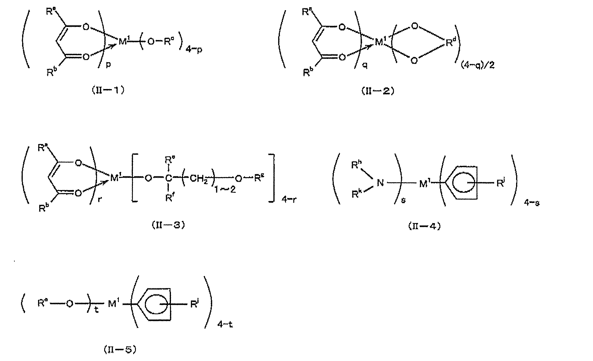
- precursors containing titanium, zirconium or hafnium include compounds represented by the following formulas (II-1) to (II-5):
- M 1 represents titanium, zirconium or hafnium, and R a and R b each independently may be substituted with a halogen atom, and may contain an oxygen atom in the chain.
- 20 represents an alkyl group
- R c represents an alkyl group having 1 to 8 carbon atoms
- R d represents an optionally branched alkylene group having 2 to 18 carbon atoms
- R e and R f are:
- R g , R h , R k and R j each independently represents a hydrogen atom or an alkyl group having 1 to 4 carbon atoms.
- P represents an integer of 0 to 4
- q represents 0 or 2
- r represents an integer of 0 to 3
- s represents an integer of 0 to 4
- t represents 1 to 4 Represents an integer.
- Examples of the alkyl group having 1 to 8 carbon atoms represented by R c include methyl, ethyl, propyl, isopropyl, butyl, secondary butyl, tertiary butyl, isobutyl, amyl, isoamyl, secondary amyl, tertiary Examples include amyl, hexyl, 1-ethylpentyl, cyclohexyl, 1-methylcyclohexyl, heptyl, isoheptyl, tertiary heptyl, n-octyl, isooctyl, tertiary octyl, 2-ethylhexyl and the like.
- the alkylene group having 2 to 18 carbon atoms which may be branched and represented by R d is a group given by glycol, and examples of the glycol include 1,2-ethanediol, 1,2 -Propanediol, 1,3-propanediol, 1,3-butanediol, 2,4-hexanediol, 2,2-dimethyl-1,3-propanediol, 2,2-diethyl-1,3-propanediol 2,2-diethyl-1,3-butanediol, 2-ethyl-2-butyl-1,3-propanediol, 2,4-pentanediol, 2-methyl-1,3-propanediol, 1-methyl -2,4-pentanediol and the like.
- Examples of the alkyl group having 1 to 3 carbon atoms represented by R e and R f include methyl, ethyl, propyl, 2-propyl and the like, and are represented by R g , R h , R j and R k .
- Examples of the alkyl group having 1 to 4 carbon atoms include methyl, ethyl, propyl, isopropyl, butyl, secondary butyl, tertiary butyl, and isobutyl.
- other precursors containing titanium include tetrakis (ethoxy) titanium, tetrakis (2-propoxy) titanium, tetrakis (butoxy) titanium, tetrakis (second butoxy) titanium, tetrakis (isobutoxy) titanium, tetrakis (first Tetrakisalkoxytitaniums such as 3 butoxy) titanium, tetrakis (tertiary amyl) titanium, tetrakis (1-methoxy-2-methyl-2-propoxy) titanium; tetrakis (pentane-2,4-dionato) titanium, (2, Tetrakis ⁇ -diketonatotitaniums such as 6-dimethylheptane-3,5-dionato) titanium, tetrakis (2,2,6,6-tetramethylheptane-3,5-dionato) titanium; bis (methoxy) bis ( Bae Tan-2,4-dionato) titanium, bis (
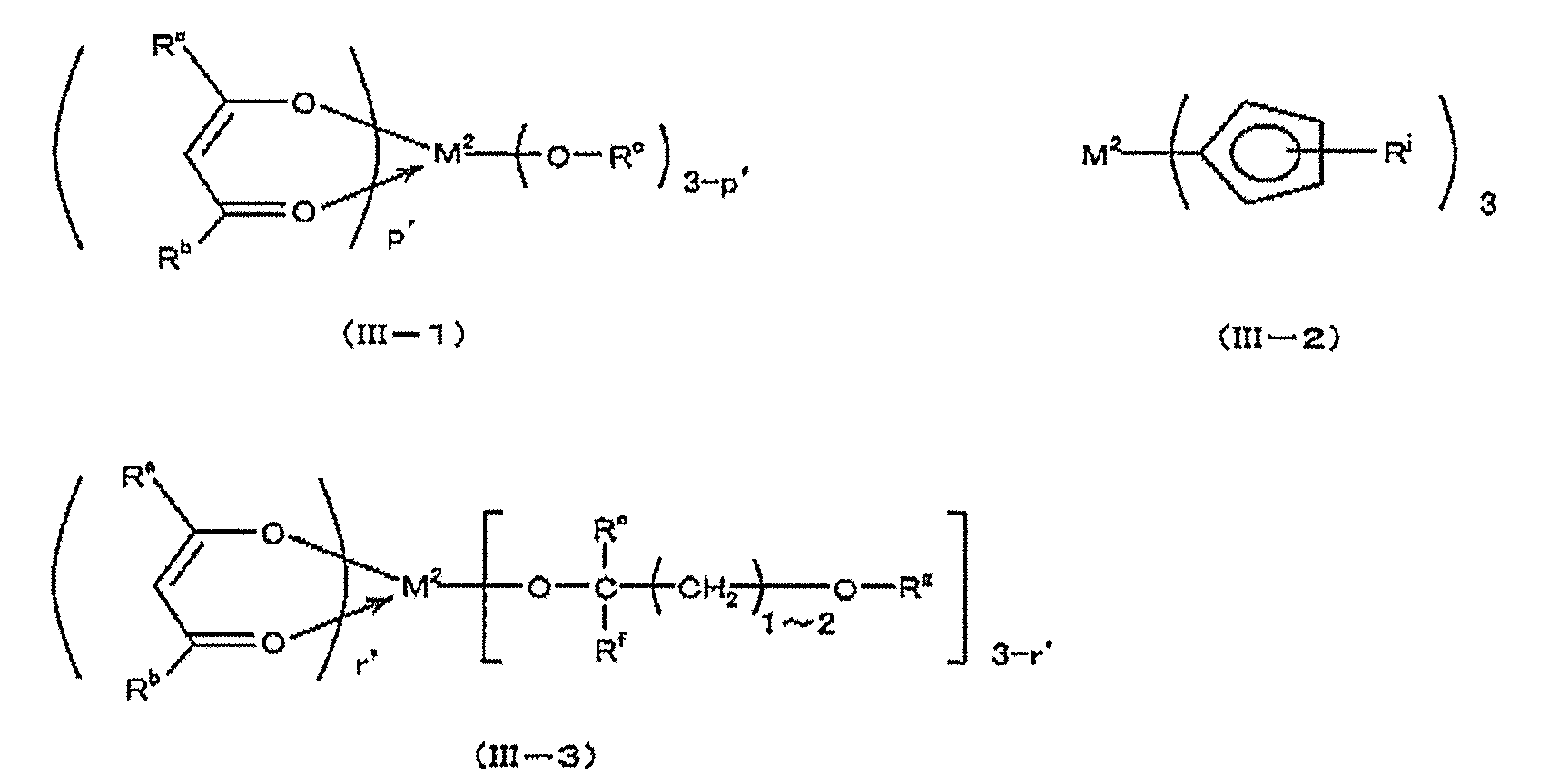
- R a and R b each independently represents an alkyl having 1 to 20 carbon atoms which may be substituted with a halogen atom and may contain an oxygen atom in the chain
- R c represents an alkyl group having 1 to 8 carbon atoms
- R e and R f each independently represents a hydrogen atom or an alkyl group having 1 to 3 carbon atoms
- R g and R j represents each independently an alkyl group having 1 to 4 carbon atoms
- p ′ represents an integer of 0 to 3
- r ′ represents an integer of 0 to 2.
- the rare earth atom represented by M 2 includes scandium, yttrium, lanthanum, cerium, praseodymium, neodymium, promethium, samarium, europium, gadolinium, terbium, dysprosium, holmium, erbium, Thulium, ytterbium, and lutetium are exemplified, and examples of the group represented by R a , R b , R c , R e , R f , R g, and R j include the groups exemplified in the above other precursors containing titanium. Can be mentioned.
- the raw material for forming a thin film of the present invention may contain a nucleophilic reagent as needed to impart the stability of the compound of the present invention and other precursors.
- the nucleophilic reagent include ethylene glycol ethers such as glyme, diglyme, triglyme and tetraglyme, 18-crown-6, dicyclohexyl-18-crown-6, 24-crown-8, dicyclohexyl-24-crown-8.
- Crown ethers such as dibenzo-24-crown-8, ethylenediamine, N, N′-tetramethylethylenediamine, diethylenetriamine, triethylenetetramine, tetraethylenepentamine, pentaethylenehexamine, 1,1,4,7,7- Polyamines such as pentamethyldiethylenetriamine, 1,1,4,7,10,10-hexamethyltriethylenetetramine and triethoxytriethyleneamine, cyclic polyamines such as cyclam and cyclen, pyridine, pyrrolidine and pipette Heterocyclic compounds such as gin, morpholine, N-methylpyrrolidine, N-methylpiperidine, N-methylmorpholine, tetrahydrofuran, tetrahydropyran, 1,4-dioxane, oxazole, thiazole, oxathiolane, methyl acetoacetate, ethyl acetoacetate, ⁇ -ketoest
- the raw material for forming a thin film of the present invention contains as little impurities metal elements as possible, impurities halogen such as impurity chlorine, and impurities organic components as much as possible.
- the impurity metal element content is preferably 100 ppb or less for each element, more preferably 10 ppb or less, and the total amount is preferably 1 ppm or less, more preferably 100 ppb or less.
- the impurity halogen content is preferably 100 ppm or less, more preferably 10 ppm or less, and most preferably 1 ppm or less. Furthermore, the total amount of impurity organic components is preferably 500 ppm or less, more preferably 50 ppm or less, and most preferably 10 ppm or less.
- each of the metal compound, organic solvent and nucleophilic reagent is preferably 10 ppm or less, more preferably 1 ppm or less.
- the raw material for forming a thin film of the present invention contains particles as little as possible in order to reduce or prevent particle contamination of the formed thin film.
- the number of particles larger than 0.3 ⁇ m is preferably 100 or less in 1 ml of the liquid phase, and larger than 0.2 ⁇ m.
- the number of particles is more preferably 1000 or less in 1 ml of the liquid phase, and the number of particles larger than 0.2 ⁇ m is most preferably 100 or less in 1 ml of the liquid phase.
- a vapor obtained by vaporizing the thin film forming raw material of the present invention and a reactive gas used as necessary are used as a substrate.
- the film is introduced into a film forming chamber in which is deposited, and then a precursor is decomposed and / or chemically reacted on the substrate to grow and deposit a metal-containing thin film on the surface of the substrate.
- a precursor is decomposed and / or chemically reacted on the substrate to grow and deposit a metal-containing thin film on the surface of the substrate.
- Examples of the reactive gas used as necessary include oxygen, ozone, nitrogen dioxide, nitric oxide, water vapor, hydrogen peroxide, formic acid, acetic acid, acetic anhydride, etc.
- Examples of reducing substances include hydrogen, and examples of nitrides that can be used include organic amine compounds such as monoalkylamines, dialkylamines, trialkylamines, and alkylenediamines, hydrazine, and ammonia. Can be used alone or in combination of two or more.
- examples of the transport and supply method include the gas transport method, the liquid transport method, the single source method, and the cocktail sauce method described above.
- the above deposition methods include thermal CVD in which a raw material gas or a raw material gas and a reactive gas are reacted only by heat to deposit a thin film, plasma CVD using heat and plasma, photo CVD using heat and light, In addition, optical plasma CVD using light and plasma, and ALD in which the deposition reaction of CVD is divided into elementary processes and deposition is performed stepwise at the molecular level.
- Examples of the material of the substrate include silicon; ceramics such as silicon nitride, titanium nitride, tantalum nitride, titanium oxide, titanium nitride, ruthenium oxide, zirconium oxide, hafnium oxide, and lanthanum oxide; glass; metals such as metal ruthenium.
- Examples of the shape of the substrate include a plate shape, a spherical shape, a fiber shape, and a scale shape, and the surface of the substrate may be a flat surface or a three-dimensional structure such as a trench structure.
- the production conditions include reaction temperature (substrate temperature), reaction pressure, deposition rate, and the like.
- the reaction temperature is preferably 100 ° C. or higher, which is the temperature at which the compound of the present invention sufficiently reacts, and more preferably 150 ° C. to 400 ° C. Since the compound of the present invention can be thermally decomposed below 250 ° C., 150 ° C. to 250 ° C. is particularly preferable.
- the reaction pressure is preferably atmospheric pressure to 10 Pa in the case of thermal CVD or photo CVD, and preferably 2000 Pa to 10 Pa in the case of using plasma.
- the deposition rate can be controlled by the raw material supply conditions (vaporization temperature, vaporization pressure), reaction temperature, and reaction pressure.
- the deposition rate is large, the properties of the obtained thin film may be deteriorated.
- productivity may be problematic. Therefore, 0.01 to 100 nm / min is preferable, and 1 to 50 nm / min is more preferable.
- the number of cycles is controlled so as to obtain a desired film thickness.
- the above production conditions include temperature and pressure at which the thin film forming raw material is vaporized into steam.
- the step of vaporizing the raw material for forming a thin film to form a vapor may be performed in a raw material container or in a vaporization chamber.
- the thin film forming raw material of the present invention is preferably evaporated at 0 to 150 ° C.
- the pressure in the raw material container and the pressure in the vaporizing chamber are both preferably 1 to 10,000 Pa.
- the thin film production method of the present invention employs the ALD method, and in addition to the raw material introduction step of vaporizing the thin film forming raw material into vapor by the above transport and supply method, and introducing the vapor into the film forming chamber, A precursor thin film forming step for forming a precursor thin film on the surface of the substrate by the compound in the vapor, an exhaust step for exhausting unreacted compound gas, and a chemical reaction of the precursor thin film with a reactive gas. And a metal-containing thin film forming step of forming a thin film containing the metal on the surface of the substrate.
- the metal oxide thin film is formed by the ALD method
- the raw material introduction step described above is performed. Preferred temperatures and pressures when the thin film forming raw material is steam are the same as those described above.
- a precursor thin film is formed on the surface of the substrate by the compound introduced into the deposition reaction part (precursor thin film forming step). At this time, heat may be applied by heating the substrate or heating the deposition reaction part.
- the precursor thin film formed in this step is a metal oxide thin film or a thin film formed by decomposition and / or reaction of a part of a compound, and has a composition different from that of the target metal oxide thin film.
- the substrate temperature when this step is performed is preferably from room temperature to 500 ° C, more preferably from 150 to 350 ° C.
- the pressure of the system (in the film forming chamber) when this step is performed is preferably 1 to 10,000 Pa, and more preferably 10 to 1000 Pa.
- exhaust process unreacted compound gas and by-product gas are exhausted from the deposition reaction part (exhaust process).
- unreacted compound gas and by-produced gas are completely exhausted from the deposition reaction part, but it is not always necessary to exhaust completely.
- the exhaust method include a method of purging the system with an inert gas such as nitrogen, helium, and argon, a method of exhausting by reducing the pressure in the system, and a method combining these.
- the degree of pressure reduction is preferably 0.01 to 300 Pa, more preferably 0.01 to 100 Pa.
- an oxidizing gas is introduced into the deposition reaction part, and a metal oxide thin film is formed from the precursor thin film obtained in the precursor thin film forming step by the action of the oxidizing gas or the action of the oxidizing gas and heat.
- Form (metal oxide-containing thin film forming step) The temperature when heat is applied in this step is preferably room temperature to 500 ° C., more preferably 150 to 350 ° C.
- the pressure of the system (in the film forming chamber) when this step is performed is preferably 1 to 10,000 Pa, and more preferably 10 to 1000 Pa.
- the compound of the present invention has good reactivity with a reducing gas, and a metal thin film can be obtained.
- the method for producing a thin film of the present invention when the ALD method is employed as described above, a series of operations including the above-described raw material introduction step, precursor thin film formation step, exhaust step, and metal oxide-containing thin film formation step
- the thin film deposition according to 1 may be set as one cycle, and this cycle may be repeated a plurality of times until a thin film having a required film thickness is obtained.
- the unreacted compound gas and reactive gas oxidizing gas in the case of forming a metal oxide thin film
- further by-produced gas from the deposition reaction part in the same manner as the exhaust process. After exhausting, it is preferable to perform the next one cycle.
- energy such as plasma, light, or voltage may be applied, or a catalyst may be used.
- the timing for applying energy and the timing for using the catalyst are not particularly limited. For example, when introducing a compound gas in the raw material introduction step, heating in the precursor thin film formation step or metal oxide-containing thin film formation step, and exhaust step At the time of evacuation in the system, at the time of introducing the oxidizing gas in the metal oxide-containing thin film forming step, it may be during the above-mentioned steps.
- annealing may be performed in an inert atmosphere, an oxidizing atmosphere, or a reducing atmosphere in order to obtain better electrical characteristics.
- a reflow process may be provided.
- the temperature in this case is 200 to 1000 ° C., preferably 250 to 500 ° C.
- a known chemical vapor deposition apparatus can be used as the apparatus for producing a thin film using the thin film forming raw material of the present invention.
- the apparatus include an apparatus that can perform a precursor as shown in FIG. 1 by bubbling supply, and an apparatus that has a vaporization chamber as shown in FIG.
- an apparatus capable of performing plasma treatment on a reactive gas can be used.
- the present invention is not limited to the single-wafer type apparatus as shown in FIGS. 1 to 4, and an apparatus capable of simultaneously processing a large number of sheets using a batch furnace may be used.
- a thin film manufactured using the raw material for forming a thin film of the present invention can be selected from other precursors, reactive gases, and manufacturing conditions as appropriate, so that a desired type of metal, oxide ceramics, nitride ceramics, glass, etc. It can be a thin film.
- Thin films are known to exhibit various electrical and optical properties and are applied to various applications. For example, copper and copper-containing thin films are applied as LSI wiring materials because of their high conductivity, high electromigration resistance, and high melting point.
- Nickel and nickel-containing thin films are mainly used for members of electronic parts such as resistance films and barrier films, members for recording media such as magnetic films, and members for thin film solar cells such as electrodes.
- Cobalt and cobalt-containing thin films are used for electrode films, resistance films, adhesive films, magnetic tapes, carbide tool members, and the like.
- Example 1 Compound No. Production of 2
- a 200 ml four-necked flask was charged with 5.02 g (0.039 mol) of cobalt (II) chloride and 19.5 g of tetrahydrofuran, and stirred at room temperature.
- a solution prepared by 5.47 g (0.039 mol) of N, N′-diisopropyl-1,4-diaza-1,3-butadiene and 40.5 g of tetrahydrofuran was added dropwise under ice cooling.
- Example 2 Compound No. Production of 3
- Into a 300 ml four-necked flask 10.0 g (0.077 mol) of cobalt (II) chloride and 54.2 g of tetrahydrofuran were charged and stirred at room temperature.
- a solution prepared by 10.9 g (0.078 mol) of N, N′-diisopropyl-1,4-diaza-1,3-butadiene and 67.7 g of tetrahydrofuran was added dropwise under ice cooling.
- Example 3 Compound No. Production of 5
- a 200 ml four-necked flask was charged with 5.09 g (0.039 mol) of cobalt (II) chloride and 44.6 g of tetrahydrofuran, and stirred at room temperature.
- 6.65 g (0.039 mol) of N, N′-di-sec-butyl-1,4-diaza-1,3-butadiene was added dropwise under ice cooling.
- Example 4 Compound No. Production of 6
- a 500 ml four-necked flask was charged with 15.0 g (0.12 mol) of cobalt (II) chloride and 45.6 g of tetrahydrofuran, and stirred at room temperature.
- a solution prepared by 19.7 g (0.12 mol) of N, N′-di-tert-butyl-1,4-diaza-1,3-butadiene and 81.9 g of tetrahydrofuran was added dropwise under ice cooling. .
- Example 5 Compound No. 9 Production
- a 200 ml four-necked flask was charged with 5.05 g (0.039 mol) of cobalt (II) chloride and 43.3 g of tetrahydrofuran, and stirred at room temperature.
- 5.60 g (0.040 mol) of N, N′-di-npropyl-1,4-diaza-1,3-butadiene was added dropwise under ice cooling.
- Example 6 Compound No. Production of 30
- a solution prepared by 4.33 g (0.031 mol) of N, N′-diisopropyl-1,4-diaza-1,3-butadiene and 19.7 g of tetrahydrofuran was added dropwise under ice cooling.
- Example 7 Compound No. Production of 39
- a 500 ml four-necked flask was charged with 10.0 g (0.080 mol) of manganese (II) chloride and 49.5 g of tetrahydrofuran, and stirred at room temperature.
- a solution prepared by 11.1 g (0.080 mol) of N, N′-diisopropyl-1,4-diaza-1,3-butadiene and 54.6 g of tetrahydrofuran was added dropwise under ice cooling.
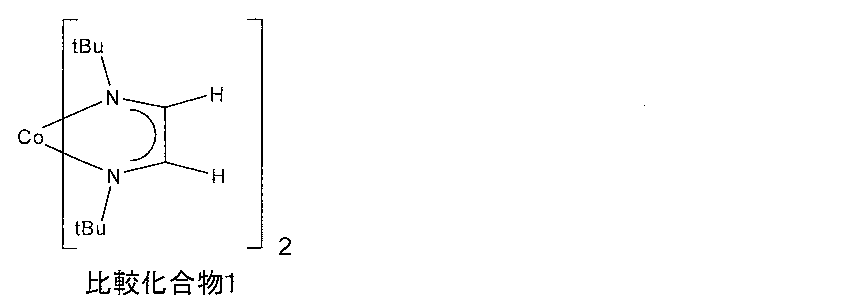
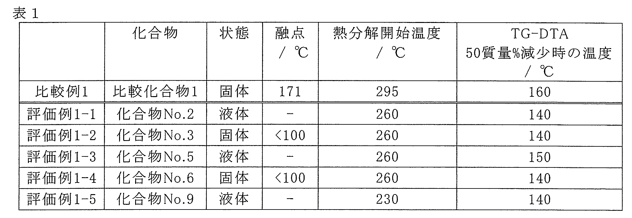
- Comparative Example 1 is a compound having a melting point of 171 ° C.
- Evaluation Examples 1-1 to 1-5 are all compounds that are liquid under normal pressure conditions of 100 ° C. . Since the raw material for forming a thin film having a low melting point is easy to transport, the raw material for forming a thin film can improve productivity. Further, from the DSC results, it was found that evaluation examples 1-1 to 1-5 started thermal decomposition at a temperature lower than that of comparative example 1. Further, from the results of TG-DTA, it was found that evaluation examples 1-1 to 1-5 had a temperature lower by 50% by mass than that of comparative example 1. From this, it was found that Evaluation Examples 1-1 to 1-5 show a vapor pressure superior to that of Comparative Example 1.
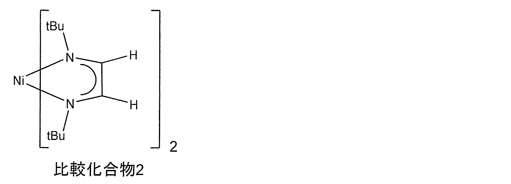
- Comparative Example 2 was a compound having a melting point of 185 ° C.
- Evaluation Example 2-1 was a compound that was liquid under normal pressure conditions of 100 ° C. Since the raw material for forming a thin film having a low melting point is easy to transport, the raw material for forming a thin film can improve productivity. From the DSC results, it was found that the thermal decomposition started in Evaluation Example 2-1 at a lower temperature than Comparative Example 2.
- Comparative Example 3 is a compound having a melting point of 155 ° C.
- Evaluation Example 3-1 is a compound that is liquid under conditions of 100 ° C. under normal pressure. Since the raw material for forming a thin film having a low melting point is easy to transport, the raw material for forming a thin film can improve productivity. From the DSC results, it was found that the thermal decomposition started in Evaluation Example 3-1 at a temperature significantly lower than that in Comparative Example 3.
- Example 8 Production of metallic cobalt thin film by ALD method 2, 3, 5, 6, and 9 were used as chemical vapor deposition raw materials, and metal cobalt thin films were each produced on a Cu substrate by the ALD method under the following conditions using the ALD apparatus shown in FIG.
- the obtained thin film was measured for film thickness by X-ray reflectivity method, confirmed by X-ray diffraction method and X-ray photoelectron spectroscopy (XPS analysis), and was confirmed to have a film thickness of 3 to 6 nm.
- the film composition was metallic cobalt (confirmed by Co2p peak by XPS analysis), and the carbon content was less than 0.1 atom% which is the lower limit of detection.
- Example 8 From the results of Example 8, it was possible to obtain a good-quality metallic cobalt thin film.
- Comparative Production Example 1 a smooth thin film could not be formed on the Cu substrate, and small lumps were found on the substrate. Moreover, since the carbon content in the Co-containing material formed on the Cu substrate was 10% or more, it was found that a high-quality metallic cobalt thin film could not be obtained.
- Example 9 Production of metallic nickel thin film by ALD method A metal nickel thin film was produced on a Cu substrate by ALD using the ALD apparatus shown in FIG. The obtained thin film was measured for film thickness by X-ray reflectivity method, confirmed by X-ray diffraction method and X-ray photoelectron spectroscopy, and the film structure and composition were confirmed to be 3 to 6 nm. Is metallic nickel (confirmed by Ni2p peak by XPS analysis), and the carbon content was less than 0.1 atom% which is the lower limit of detection. The film thickness obtained per cycle was 0.02 to 0.04 nm.
- Reaction temperature (substrate temperature): 220 ° C.
- reactive gas hydrogen gas
- Example 10 Production of metal manganese thin film by ALD method A metal manganese thin film was produced on a Cu substrate by ALD using the ALD apparatus shown in FIG. The obtained thin film was measured for film thickness by X-ray reflectivity method, confirmed by X-ray diffraction method and X-ray photoelectron spectroscopy, and the film structure and composition were confirmed to be 3 to 6 nm. Is metal manganese (confirmed by Mn2p peak by XPS analysis), and the carbon content was less than 0.1 atom% which is the lower limit of detection. The film thickness obtained per cycle was 0.02 to 0.04 nm.
- Reaction temperature (substrate temperature): 240 ° C.
- reactive gas hydrogen gas
Landscapes
- Chemical & Material Sciences (AREA)
- Organic Chemistry (AREA)
- General Chemical & Material Sciences (AREA)
- Chemical Kinetics & Catalysis (AREA)
- Engineering & Computer Science (AREA)
- Materials Engineering (AREA)
- Mechanical Engineering (AREA)
- Metallurgy (AREA)
- Chemical Vapour Deposition (AREA)
- Electrodes Of Semiconductors (AREA)
Abstract
Description
即ち、本発明は、下記一般式(I)または下記一般式(II)で表される新規な化合物、これを含有してなる薄膜形成用原料及び該原料を用いた薄膜の製造方法を提供するものである:

気化工程を伴わないMOD法による薄膜の製造方法の場合は、R1及びR2は、使用される溶媒に対する溶解性、薄膜形成反応等によって任意に選択することができる。


例えば、本発明の一般式(I)で表される化合物のうち、コバルトの化合物を製造する場合には、コバルトのハロゲン化物、硝酸塩等の無機塩又はその水和物と、該当するジアザジエン化合物とを反応させる方法;コバルトのハロゲン化物、硝酸塩等の無機塩又はその水和物と、該当するジアザジエン化合物を反応させる方法などを利用することができる。
また、本発明の一般式(II)で表される化合物のうち、コバルトのジアザジエニル化合物を製造する場合には、例えば、コバルトのハロゲン化物、硝酸塩等の無機塩又はその水和物と、該当するジアザジエン化合物とを、ナトリウム、リチウム、水素化ナトリウム、ナトリウムアミド、水酸化ナトリウム、ナトリウムメチラート、アンモニア、アミン等の塩基の存在下で反応させる方法;コバルトのハロゲン化物、硝酸塩等の無機塩又はその水和物と、該当するジアザジエン化合物のナトリウム錯体、リチウム錯体、カリウム錯体等を反応させる方法;本発明の一般式(I)で表される化合物の不均化などを利用することができる。
[実施例1:化合物No.2の製造]
200mlの4つ口フラスコに、塩化コバルト(II)5.02g(0.039mol)、テトラヒドロフラン19.5gを仕込み、室温下で撹拌した。その中に、N,N’-ジイソプロプル-1,4-ジアザ-1,3-ブタジエン5.47g(0.039mol)、テトラヒドロフラン40.5gにより調製した溶液を氷冷下で滴下した。次いで、N,N’-ジ-sec-ブチル-1,4-ジアザ-1,3-ブタジエン7.50g(0.044mol)、テトラヒドロフラン39.1g、Li0.59g(0.085mol)により調製した溶液を滴下し、滴下後室温に戻し17時間攪拌し、濾過を行った。得られた濾液から溶媒を除去し、残渣をバス温度140℃、圧力96Pa、塔頂温度120℃で蒸留を行い、暗褐色液体を得た。収量は8.20g、収率は58%であった。
(分析値)
(1)常圧TG-DTA
質量50%減少温度:226℃(Ar流量:100ml/分、昇温10℃/分、サンプル量:9.766mg)
(2)減圧TG-DTA
質量50%減少温度:145℃(10Torr、Ar流量:50ml/分、昇温10℃/分、サンプル量:9.821mg)
(3)元素分析(金属分析:ICP-AES)
コバルト含有量:16.5質量%(理論値 16.04質量%)
CHN分析:C59.6%(理論値58.9%)、H10.0%(理論値9.9%)、N15.1%(理論値15.3%)
300mlの4つ口フラスコに、塩化コバルト(II)10.0g(0.077mol)、テトラヒドロフラン54.2gを仕込み、室温下で撹拌した。その中に、N,N’-ジイソプロピル-1,4-ジアザ-1,3-ブタジエン10.9g(0.078mol)、テトラヒドロフラン67.7gにより調製した溶液を氷冷下で滴下した。次いでN,N’-ジ-tert-ブチル-1,4-ジアザ-1,3-ブタジエン14.3g(0.085mol)、テトラヒドロフラン82.9g、Li1.19g(0.17mol)により調製した溶液を滴下し、滴下後室温に戻し15時間攪拌した。バス温度100℃、微減圧下で溶媒を留去した後、n-ヘプタンにより溶媒交換を行い、濾過を行った。得られた濾液から溶媒を除去し、残渣をバス温度140℃、圧力54Pa、塔頂温度114℃で蒸留を行い、濃褐色固体を得た。収量は23.2g、収率は82%であった。
(分析値)
(1)常圧TG-DTA
質量50%減少温度:231℃(Ar流量:100ml/分、昇温10℃/分、サンプル量:10.21mg)
(2)減圧TG-DTA
質量50%減少温度:146℃(10Torr、Ar流量:50ml/分、昇温10℃/分、サンプル量:9.324mg)
(3)元素分析(金属分析:ICP-AES)
コバルト含有量:16.0質量%(理論値 16.04質量%)
CHN分析:C59.0%(理論値58.9%)、H10.0%(理論値9.9%)、N15.1%(理論値15.3%)
200mlの4つ口フラスコに、塩化コバルト(II)5.09g(0.039mol)、テトラヒドロフラン44.6gを仕込み、室温下で撹拌した。その中に、N,N’-ジ-sec-ブチル-1,4-ジアザ-1,3-ブタジエン6.65g(0.039mol)を氷冷下で滴下した。次いでN,N’-ジイソプロピル-1,4-ジアザ-1,3-ブタジエン5.97g(0.042mol)、テトラヒドロフラン38.0g、Li0.59g(0.085mol)により調製した溶液を滴下し、滴下後室温に戻し21時間攪拌し、濾過を行った。得られた濾液から溶媒を除去し、残渣をバス温度145℃、圧力90Pa、塔頂温度129℃で蒸留を行い、暗褐色液体を得た。収量は7.28g、収率は51%であった。
(分析値)
(1)常圧TG-DTA
質量50%減少温度:230℃(Ar流量:100ml/分、昇温10℃/分、サンプル量:9.737mg)
(2)減圧TG-DTA
質量50%減少温度:149℃(10Torr、Ar流量:50ml/分、昇温10℃/分、サンプル量:9.802mg)
(3)元素分析(金属分析:ICP-AES)
コバルト含有量:16.2質量%(理論値 16.04質量%)
CHN分析:C58.1%(理論値58.9%)、H9.3%(理論値9.9%)、N15.1%(理論値15.7%)
500mlの4つ口フラスコに、塩化コバルト(II)15.0g(0.12mol)、テトラヒドロフラン45.6gを仕込み、室温下で撹拌した。その中に、N,N’-ジ-tert-ブチル-1,4-ジアザ-1,3-ブタジエン19.7g(0.12mol)、テトラヒドロフラン81.9gにより調製した溶液を氷冷下で滴下した。次いでN,N’-ジイソプロピル-1,4-ジアザ-1,3-ブタジエン17.8g(0.12mol)、テトラヒドロフラン121g、Li1.76g(0.25mol)により調製した溶液を滴下し、滴下後室温に戻し18時間攪拌した。バス温度95℃、微減圧下で溶媒を留去した後、n-ヘプタンにより溶媒交換を行い、濾過を行った。得られた濾液から溶媒を除去し、残渣をバス温度140℃、圧力110Pa、塔頂温度133℃で蒸留を行い、濃褐色固体を得た。収量は25.4g、収率は60%であった。
(分析値)
(1)常圧TG-DTA
質量50%減少温度:227℃(Ar流量:100ml/分、昇温10℃/分、サンプル量:10.00mg)
(2)減圧TG-DTA
質量50%減少温度:144℃(10Torr、Ar流量:50ml/分、昇温10℃/分、サンプル量:10.07mg)
(3)元素分析(金属分析:ICP-AES)
コバルト含有量:16.1質量%(理論値 16.04質量%)
CHN分析:C58.7%(理論値58.9%)、H9.2%(理論値9.9%)、N15.9%(理論値15.3%)
200mlの4つ口フラスコに、塩化コバルト(II)5.05g(0.039mol)、テトラヒドロフラン43.3gを仕込み、室温下で撹拌した。その中に、N,N’-ジ-nプロピル-1,4-ジアザ-1,3-ブタジエン5.60g(0.040mol)を氷冷下で滴下した。次いでN,N’-ジ-tert-ブチル-1,4-ジアザ-1,3-ブタジエン7.36g(0.044mol)、テトラヒドロフラン40.8g、Li0.59g(0.085mol)により調製した溶液を滴下し、滴下後室温に戻し17時間攪拌した。バス温度90℃、微減圧下で溶媒を留去した後、n-ヘプタンにより溶媒交換を行い、濾過を行った。得られた濾液から溶媒を除去し、残渣をバス温度145℃、圧力56Pa、塔頂温度110℃で蒸留を行い、濃緑色液体を得た。収量は6.97g、収率は49%であった。
(分析値)
(1)常圧TG-DTA
質量50%減少温度:227℃(Ar流量:100ml/分、昇温10℃/分、サンプル量:9.688mg)
(2)減圧TG-DTA
質量50%減少温度:146℃(10Torr、Ar流量:50ml/分、昇温10℃/分、サンプル量:10.31mg)
(3)元素分析(金属分析:ICP-AES)
コバルト含有量:16.2質量%(理論値 16.04質量%)
CHN分析:C58.2%(理論値58.9%)、H9.3%(理論値9.9%)、N15.7%(理論値15.3%)
200mlの4つ口フラスコに、塩化ニッケル(II)4.0g(0.031mol)、テトラヒドロフラン23.8gを仕込み、室温下で撹拌した。その中に、N,N’-ジイソプロピル-1,4-ジアザ-1,3-ブタジエン4.33g(0.031mol)、テトラヒドロフラン19.7gにより調製した溶液を氷冷下で滴下した。次いでN,N’-ジ-tert-ブチル-1,4-ジアザ-1,3-ブタジエン5.19g(0.031mol)、テトラヒドロフラン37.4g、Li0.42g(0.062mol)により調製した溶液を滴下し、滴下後室温に戻し20時間攪拌した。バス温度70℃、微減圧下で溶媒を留去した後、n-ヘキサンにより溶媒交換を行い、濾過を行った。得られた濾液から溶媒を除去し、クーゲルロールを用いて残渣を105℃、30Paの条件下で精製して暗赤色固体を得た。収量は1.81g、収率は16%であった。
(分析値)
(1)常圧TG-DTA
質量50%減少温度:210℃(Ar流量:100ml/分、昇温10℃/分、サンプル量:9.980mg)
(2)減圧TG-DTA
質量50%減少温度:142℃(10Torr、Ar流量:50ml/分、昇温10℃/分、サンプル量:9.698mg)
(3)1H-NMR(溶媒:重ベンゼン)(ケミカルシフト:多重度:H数)
(8.934-8.948:d:2)(8.733-8.738:d:2)(2.785-2.834:m:1)(2.603-2.667:m:1)(1.941:s:9)(1.908-1.925:d:6)(1.899:s:9)(1.839-1.856:d:6)
(4)元素分析(金属分析:ICP-AES)
ニッケル含有量:質量16.2%(理論値質量16.0%)
CHN分析:C59.3%(理論値58.9%)、H10.2%(理論値9.9%)、N15.9%(理論値15.3%)
500mlの4つ口フラスコに、塩化マンガン(II)10.0g(0.080mol)、テトラヒドロフラン49.5gを仕込み、室温下で撹拌した。その中に、N,N’-ジイソプロピル-1,4-ジアザ-1,3-ブタジエン11.1g(0.080mol)、テトラヒドロフラン54.6gにより調製した溶液を氷冷下で滴下した。次いでN,N’-ジ-tert-ブチル-1,4-ジアザ-1,3-ブタジエン13.4g(0.080mol)、テトラヒドロフラン79.2g、Li1.10g(0.16mol)により調製した溶液を滴下し、滴下後室温に戻し15時間攪拌した。バス温度90℃、微減圧下で溶媒を留去した後、n-ヘキサンにより溶媒交換を行い、濾過を行った。得られた濾液から溶媒を除去し、残渣をバス温度128℃、圧力60Pa、塔頂温度118℃で蒸留を行い、黒色固体である目的物を得た。収量は12.8g、収率は44%であった。
(分析値)
(1)常圧TG-DTA
質量50%減少温度:219℃(Ar流量:100ml/分、昇温10℃/分、サンプル量:9.805mg)
(2)減圧TG-DTA
質量50%減少温度:140℃(10Torr、Ar流量:50ml/分、昇温10℃/分、サンプル量:9.847mg)
(3)元素分析(金属分析:ICP-AES)
マンガン含有量:15.5質量%(理論値15.1質量%)
CHN分析:C60.3%(理論値59.5%)、H10.2%(理論値10.0%)、N15.2%(理論値15.4%)
化合物No.2、3、5、6および9並びに下記に示す比較化合物1について、目視によって常圧30℃における各化合物の状態を観察し、固体化合物については微小融点測定装置を用いて融点を測定した。化合物No.2、3、5、6および9並びに下記に示す比較化合物1について、示差操作熱量測定(DSC)を用いて熱分解が開始する温度を測定した。化合物No.2、3、5、6および9並びに下記に示す比較化合物1について、TG-DTAを用いて重量が50%減少した際の温度を測定した。結果を表1に示す。
TD-GTA測定条件:10Torr、Ar流量:50ml/分、昇温10℃/分、サンプル量約10mg
化合物No.30及び下記に示す比較化合物2について、目視によって常圧30℃における各化合物の状態を観察し、固体化合物については微小融点測定装置を用いて融点を測定した。化合物No.30及び下記に示す比較化合物2について、DSCを用いて熱分解が開始する温度を測定した。結果を表2に示す。

化合物No.39及び下記に示す比較化合物3について、目視によって常圧30℃における各化合物の状態を観察し、固体化合物については微小融点測定装置を用いて融点を測定した。化合物No.39及び下記に示す比較化合物3について、DSCを用いて熱分解が開始する温度を測定した。結果を表3に示す。


化合物No.2、3、5、6および9を化学気相成長用原料とし、図1に示すALD装置を用いて以下の条件のALD法により、Cu基板上に各々金属コバルト薄膜を製造した。得られた薄膜について、X線反射率法による膜厚測定、X線回折法及びX線光電子分光法(XPS分析)による薄膜構造及び薄膜組成の確認を行ったところ、膜厚は3~6nmであり、膜組成は金属コバルト(XPS分析によるCo2pピークで確認)であり、炭素含有量は検出下限である0.1atom%よりも少なかった。1サイクル当たりに得られる膜厚は、0.02~0.04nmであった。
(条件)
反応温度(基板温度):270℃、反応性ガス:水素ガス
(工程)
下記(1)~(4)からなる一連の工程を1サイクルとして、150サイクル繰り返した:
(1)原料容器加熱温度:100℃、原料容器内圧力100Paの条件で気化させた化学気相成長用原料の蒸気を導入し、系圧100Paで30秒間堆積させる;
(2)5秒間のアルゴンパージにより、未反応原料を除去する;
(3)反応性ガスを導入し、系圧力100Paで30秒間反応させる;
(4)5秒間のアルゴンパージにより、未反応原料を除去する。
比較化合物1を化学気相成長用原料とし、実施例8と同様の方法でCu基板上に金属コバルト薄膜の製造を試みたが、平滑な薄膜を得ることはできなかった。Cu基板上に形成されたCo含有物中の炭素含有量は10%以上であった。
(条件)
反応温度(基板温度):270℃、反応性ガス:水素ガス
(工程)
下記(1)~(4)からなる一連の工程を1サイクルとして、150サイクル繰り返した:
(1)原料容器加熱温度:100℃、原料容器内圧力100Paの条件で気化させた化学気相成長用原料の蒸気を導入し、系圧100Paで30秒間堆積させる;
(2)5秒間のアルゴンパージにより、未反応原料を除去する;
(3)反応性ガスを導入し、系圧力100Paで30秒間反応させる;
(4)5秒間のアルゴンパージにより、未反応原料を除去する。
化合物No.30を化学気相成長用原料とし、図1に示すALD装置を用いて以下の条件のALD法により、Cu基板上に金属ニッケル薄膜を製造した。得られた薄膜について、X線反射率法による膜厚測定、X線回折法及びX線光電子分光法による薄膜構造及び薄膜組成の確認を行ったところ、膜厚は3~6nmであり、膜組成は金属ニッケル(XPS分析によるNi2pピークで確認)であり、炭素含有量は検出下限である0.1atom%よりも少なかった。1サイクル当たりに得られる膜厚は、0.02~0.04nmであった。
(条件)
反応温度(基板温度):220℃、反応性ガス:水素ガス
(工程)
下記(1)~(4)からなる一連の工程を1サイクルとして、150サイクル繰り返した:
(1)原料容器加熱温度:100℃、原料容器内圧力100Paの条件で気化させた化学気相成長用原料の蒸気を導入し、系圧100Paで30秒間堆積させる;
(2)5秒間のアルゴンパージにより、未反応原料を除去する;
(3)反応性ガスを導入し、系圧力100Paで30秒間反応させる;
(4)5秒間のアルゴンパージにより、未反応原料を除去する。
化合物No.39を化学気相成長用原料とし、図1に示すALD装置を用いて以下の条件のALD法により、Cu基板上に金属マンガン薄膜を製造した。得られた薄膜について、X線反射率法による膜厚測定、X線回折法及びX線光電子分光法による薄膜構造及び薄膜組成の確認を行ったところ、膜厚は3~6nmであり、膜組成は金属マンガン(XPS分析によるMn2pピークで確認)であり、炭素含有量は検出下限である0.1atom%よりも少なかった。1サイクル当たりに得られる膜厚は、0.02~0.04nmであった。
(条件)
反応温度(基板温度):240℃、反応性ガス:水素ガス
(工程)
下記(1)~(4)からなる一連の工程を1サイクルとして、150サイクル繰り返した:
(1)原料容器加熱温度:100℃、原料容器内圧力100Paの条件で気化させた化学気相成長用原料の蒸気を導入し、系圧100Paで30秒間堆積させる;
(2)5秒間のアルゴンパージにより、未反応原料を除去する;
(3)反応性ガスを導入し、系圧力100Paで30秒間反応させる;
(4)5秒間のアルゴンパージにより、未反応原料を除去する。
Claims (5)
- 下記一般式(I)または(II)で表される化合物:


- 一般式(I)または一般式(II)において、Mが銅、鉄、ニッケル、コバルト又はマンガンである、請求項1に記載の化合物。
- 一般式(I)または一般式(II)において、nが1である、請求項1または2に記載の化合物。
- 請求項1ないし3のいずれか一項に記載の化合物を含有してなる薄膜形成用原料。
- 請求項4に記載の薄膜形成用原料を気化させて得られる化合物を含有する蒸気を、基体が設置された成膜チャンバー内に導入し、該化合物を分解及び/又は化学反応させて該基体の表面に金属原子及びケイ素原子から選ばれる少なくとも1種の原子を含有する薄膜を形成する薄膜の製造方法。
Priority Applications (5)
| Application Number | Priority Date | Filing Date | Title |
|---|---|---|---|
| CN201680025896.6A CN107531734A (zh) | 2015-06-17 | 2016-05-17 | 新型的化合物、薄膜形成用原料和薄膜的制造方法 |
| EP16811362.9A EP3312187A4 (en) | 2015-06-17 | 2016-05-17 | METHOD FOR PRODUCING A NOVEL COMPOUND, RAW MATERIAL FOR THIN LAYERING AND THIN LAYER |
| KR1020187000230A KR102541122B1 (ko) | 2015-06-17 | 2016-05-17 | 신규 화합물, 박막 형성용 원료 및 박막의 제조 방법 |
| US15/559,127 US10253408B2 (en) | 2015-06-17 | 2016-05-17 | Compound, thin film-forming material, and thin film manufacturing method |
| IL255614A IL255614B (en) | 2015-06-17 | 2017-11-12 | Novel compound, thin film-forming material, and thin film manufacturing method |
Applications Claiming Priority (2)
| Application Number | Priority Date | Filing Date | Title |
|---|---|---|---|
| JP2015121840A JP6675159B2 (ja) | 2015-06-17 | 2015-06-17 | 新規な化合物、薄膜形成用原料及び薄膜の製造方法 |
| JP2015-121840 | 2015-06-17 |
Publications (1)
| Publication Number | Publication Date |
|---|---|
| WO2016203887A1 true WO2016203887A1 (ja) | 2016-12-22 |
Family
ID=57545126
Family Applications (1)
| Application Number | Title | Priority Date | Filing Date |
|---|---|---|---|
| PCT/JP2016/064573 Ceased WO2016203887A1 (ja) | 2015-06-17 | 2016-05-17 | 新規な化合物、薄膜形成用原料及び薄膜の製造方法 |
Country Status (8)
| Country | Link |
|---|---|
| US (1) | US10253408B2 (ja) |
| EP (1) | EP3312187A4 (ja) |
| JP (1) | JP6675159B2 (ja) |
| KR (1) | KR102541122B1 (ja) |
| CN (1) | CN107531734A (ja) |
| IL (1) | IL255614B (ja) |
| TW (1) | TWI691503B (ja) |
| WO (1) | WO2016203887A1 (ja) |
Cited By (1)
| Publication number | Priority date | Publication date | Assignee | Title |
|---|---|---|---|---|
| WO2017221586A1 (ja) * | 2016-06-22 | 2017-12-28 | 株式会社Adeka | バナジウム化合物、薄膜形成用原料及び薄膜の製造方法 |
Families Citing this family (6)
| Publication number | Priority date | Publication date | Assignee | Title |
|---|---|---|---|---|
| US10106893B1 (en) * | 2017-04-07 | 2018-10-23 | Applied Materials, Inc. | Iridium precursors for ALD and CVD thin film deposition and uses thereof |
| KR102474876B1 (ko) * | 2017-06-15 | 2022-12-07 | 삼성전자주식회사 | 텅스텐 전구체 및 이를 이용한 텅스텐 함유막의 형성 방법 |
| US11440929B2 (en) * | 2018-06-19 | 2022-09-13 | Versum Materials Us, Llc | Bis(diazadiene)cobalt compounds, method of making and method of use thereof |
| KR102123331B1 (ko) * | 2018-12-19 | 2020-06-17 | 주식회사 한솔케미칼 | 코발트 전구체, 이의 제조방법 및 이를 이용한 박막의 제조방법 |
| CN110128373B (zh) * | 2019-06-12 | 2023-03-24 | 鸿翌科技有限公司 | 哌嗪基锡配合物及其制备方法、薄膜、太阳能电池 |
| IL326480A (en) * | 2023-09-04 | 2026-04-01 | Adeka Corp | Raw material for forming a thin layer, a thin layer, a method for producing a thin layer, and a lanthanum compound |
Citations (3)
| Publication number | Priority date | Publication date | Assignee | Title |
|---|---|---|---|---|
| WO2012176989A1 (en) * | 2011-06-24 | 2012-12-27 | Up Chemical Co., Ltd. | A diamine compound or its salt, preparing method of the same, and uses of the same |
| JP2013545755A (ja) * | 2010-11-17 | 2013-12-26 | ユーピー ケミカル カンパニー リミテッド | ジアザジエン系金属化合物、これの製造方法及びこれを利用した薄膜形成方法 |
| US20150105573A1 (en) * | 2013-10-14 | 2015-04-16 | Patricio E. Romero | Scalable And High Yield Synthesis Of Transition Metal Bis-Diazabutadienes |
Family Cites Families (2)
| Publication number | Priority date | Publication date | Assignee | Title |
|---|---|---|---|---|
| US9255327B2 (en) | 2010-08-24 | 2016-02-09 | Wayne State University | Thermally stable volatile precursors |
| WO2013046157A1 (en) * | 2011-09-27 | 2013-04-04 | L'air Liquide, Societe Anonyme Pour L'etude Et L'exploitation Des Procedes Georges Claude | Nickel bis diazabutadiene precursors, their synthesis, and their use for nickel containing film depositions |
-
2015
- 2015-06-17 JP JP2015121840A patent/JP6675159B2/ja active Active
-
2016
- 2016-05-17 KR KR1020187000230A patent/KR102541122B1/ko active Active
- 2016-05-17 EP EP16811362.9A patent/EP3312187A4/en active Pending
- 2016-05-17 WO PCT/JP2016/064573 patent/WO2016203887A1/ja not_active Ceased
- 2016-05-17 CN CN201680025896.6A patent/CN107531734A/zh active Pending
- 2016-05-17 US US15/559,127 patent/US10253408B2/en active Active
- 2016-05-25 TW TW105116286A patent/TWI691503B/zh active
-
2017
- 2017-11-12 IL IL255614A patent/IL255614B/en unknown
Patent Citations (3)
| Publication number | Priority date | Publication date | Assignee | Title |
|---|---|---|---|---|
| JP2013545755A (ja) * | 2010-11-17 | 2013-12-26 | ユーピー ケミカル カンパニー リミテッド | ジアザジエン系金属化合物、これの製造方法及びこれを利用した薄膜形成方法 |
| WO2012176989A1 (en) * | 2011-06-24 | 2012-12-27 | Up Chemical Co., Ltd. | A diamine compound or its salt, preparing method of the same, and uses of the same |
| US20150105573A1 (en) * | 2013-10-14 | 2015-04-16 | Patricio E. Romero | Scalable And High Yield Synthesis Of Transition Metal Bis-Diazabutadienes |
Non-Patent Citations (1)
| Title |
|---|
| See also references of EP3312187A4 * |
Cited By (3)
| Publication number | Priority date | Publication date | Assignee | Title |
|---|---|---|---|---|
| WO2017221586A1 (ja) * | 2016-06-22 | 2017-12-28 | 株式会社Adeka | バナジウム化合物、薄膜形成用原料及び薄膜の製造方法 |
| EP3476827A4 (en) * | 2016-06-22 | 2019-12-25 | Adeka Corporation | VANADIUM CONNECTION, INITIAL MATERIAL FOR FORMING A THIN LAYER AND METHOD FOR PRODUCING A THIN LAYER |
| US10882874B2 (en) | 2016-06-22 | 2021-01-05 | Adeka Corporation | Vanadium compound |
Also Published As
| Publication number | Publication date |
|---|---|
| KR102541122B1 (ko) | 2023-06-08 |
| CN107531734A (zh) | 2018-01-02 |
| IL255614A (en) | 2018-01-31 |
| IL255614B (en) | 2021-08-31 |
| US10253408B2 (en) | 2019-04-09 |
| JP2017007952A (ja) | 2017-01-12 |
| TW201714890A (zh) | 2017-05-01 |
| KR20180022775A (ko) | 2018-03-06 |
| TWI691503B (zh) | 2020-04-21 |
| EP3312187A1 (en) | 2018-04-25 |
| JP6675159B2 (ja) | 2020-04-01 |
| US20180051372A1 (en) | 2018-02-22 |
| EP3312187A4 (en) | 2019-04-10 |
Similar Documents
| Publication | Publication Date | Title |
|---|---|---|
| JP6465699B2 (ja) | ジアザジエニル化合物、薄膜形成用原料、薄膜の製造方法及びジアザジエン化合物 | |
| US10882874B2 (en) | Vanadium compound | |
| JP6675159B2 (ja) | 新規な化合物、薄膜形成用原料及び薄膜の製造方法 | |
| JP6184030B2 (ja) | アルミニウム化合物、薄膜形成用原料及び薄膜の製造方法 | |
| US11618762B2 (en) | Compound, raw material for forming thin film, method for manufacturing thin film, and amidine compound | |
| KR102375179B1 (ko) | 알콕사이드 화합물, 박막 형성용 원료, 박막의 제조방법 및 알코올 화합물 | |
| US10920313B2 (en) | Diazadienyl compound, raw material for forming thin film, and method for manufacturing thin film | |
| JP6662779B2 (ja) | アルコキシド化合物、薄膜形成用原料、薄膜の形成方法及びアルコール化合物 | |
| JP6408178B2 (ja) | アルコキシド化合物 |
Legal Events
| Date | Code | Title | Description |
|---|---|---|---|
| 121 | Ep: the epo has been informed by wipo that ep was designated in this application |
Ref document number: 16811362 Country of ref document: EP Kind code of ref document: A1 |
|
| WWE | Wipo information: entry into national phase |
Ref document number: 15559127 Country of ref document: US |
|
| WWE | Wipo information: entry into national phase |
Ref document number: 255614 Country of ref document: IL |
|
| NENP | Non-entry into the national phase |
Ref country code: DE |
|
| ENP | Entry into the national phase |
Ref document number: 20187000230 Country of ref document: KR Kind code of ref document: A |