WO2016203899A1 - 半導体装置用ボンディングワイヤ - Google Patents
半導体装置用ボンディングワイヤ Download PDFInfo
- Publication number
- WO2016203899A1 WO2016203899A1 PCT/JP2016/064926 JP2016064926W WO2016203899A1 WO 2016203899 A1 WO2016203899 A1 WO 2016203899A1 JP 2016064926 W JP2016064926 W JP 2016064926W WO 2016203899 A1 WO2016203899 A1 WO 2016203899A1
- Authority
- WO
- WIPO (PCT)
- Prior art keywords
- wire
- bonding
- bonding wire
- concentration
- mass
- Prior art date
- Legal status (The legal status is an assumption and is not a legal conclusion. Google has not performed a legal analysis and makes no representation as to the accuracy of the status listed.)
- Ceased
Links
Classifications
-
- H—ELECTRICITY
- H10—SEMICONDUCTOR DEVICES; ELECTRIC SOLID-STATE DEVICES NOT OTHERWISE PROVIDED FOR
- H10W—GENERIC PACKAGES, INTERCONNECTIONS, CONNECTORS OR OTHER CONSTRUCTIONAL DETAILS OF DEVICES COVERED BY CLASS H10
- H10W72/00—Interconnections or connectors in packages
- H10W72/01—Manufacture or treatment
- H10W72/011—Apparatus therefor
- H10W72/0115—Apparatus for manufacturing bond wires
-
- H—ELECTRICITY
- H10—SEMICONDUCTOR DEVICES; ELECTRIC SOLID-STATE DEVICES NOT OTHERWISE PROVIDED FOR
- H10W—GENERIC PACKAGES, INTERCONNECTIONS, CONNECTORS OR OTHER CONSTRUCTIONAL DETAILS OF DEVICES COVERED BY CLASS H10
- H10W72/00—Interconnections or connectors in packages
- H10W72/01—Manufacture or treatment
- H10W72/015—Manufacture or treatment of bond wires
-
- H—ELECTRICITY
- H10—SEMICONDUCTOR DEVICES; ELECTRIC SOLID-STATE DEVICES NOT OTHERWISE PROVIDED FOR
- H10W—GENERIC PACKAGES, INTERCONNECTIONS, CONNECTORS OR OTHER CONSTRUCTIONAL DETAILS OF DEVICES COVERED BY CLASS H10
- H10W72/00—Interconnections or connectors in packages
- H10W72/071—Connecting or disconnecting
- H10W72/0711—Apparatus therefor
-
- H—ELECTRICITY
- H10—SEMICONDUCTOR DEVICES; ELECTRIC SOLID-STATE DEVICES NOT OTHERWISE PROVIDED FOR
- H10W—GENERIC PACKAGES, INTERCONNECTIONS, CONNECTORS OR OTHER CONSTRUCTIONAL DETAILS OF DEVICES COVERED BY CLASS H10
- H10W72/00—Interconnections or connectors in packages
- H10W72/50—Bond wires
-
- H—ELECTRICITY
- H10—SEMICONDUCTOR DEVICES; ELECTRIC SOLID-STATE DEVICES NOT OTHERWISE PROVIDED FOR
- H10W—GENERIC PACKAGES, INTERCONNECTIONS, CONNECTORS OR OTHER CONSTRUCTIONAL DETAILS OF DEVICES COVERED BY CLASS H10
- H10W72/00—Interconnections or connectors in packages
- H10W72/01—Manufacture or treatment
- H10W72/015—Manufacture or treatment of bond wires
- H10W72/01565—Thermally treating
-
- H—ELECTRICITY
- H10—SEMICONDUCTOR DEVICES; ELECTRIC SOLID-STATE DEVICES NOT OTHERWISE PROVIDED FOR
- H10W—GENERIC PACKAGES, INTERCONNECTIONS, CONNECTORS OR OTHER CONSTRUCTIONAL DETAILS OF DEVICES COVERED BY CLASS H10
- H10W72/00—Interconnections or connectors in packages
- H10W72/50—Bond wires
- H10W72/521—Structures or relative sizes of bond wires
- H10W72/522—Multilayered bond wires, e.g. having a coating concentric around a core
- H10W72/523—Multilayered bond wires, e.g. having a coating concentric around a core characterised by the structures of the outermost layers, e.g. multilayered coatings
-
- H—ELECTRICITY
- H10—SEMICONDUCTOR DEVICES; ELECTRIC SOLID-STATE DEVICES NOT OTHERWISE PROVIDED FOR
- H10W—GENERIC PACKAGES, INTERCONNECTIONS, CONNECTORS OR OTHER CONSTRUCTIONAL DETAILS OF DEVICES COVERED BY CLASS H10
- H10W72/00—Interconnections or connectors in packages
- H10W72/50—Bond wires
- H10W72/551—Materials of bond wires
- H10W72/552—Materials of bond wires comprising metals or metalloids, e.g. silver
- H10W72/5522—Materials of bond wires comprising metals or metalloids, e.g. silver comprising gold [Au]
-
- H—ELECTRICITY
- H10—SEMICONDUCTOR DEVICES; ELECTRIC SOLID-STATE DEVICES NOT OTHERWISE PROVIDED FOR
- H10W—GENERIC PACKAGES, INTERCONNECTIONS, CONNECTORS OR OTHER CONSTRUCTIONAL DETAILS OF DEVICES COVERED BY CLASS H10
- H10W72/00—Interconnections or connectors in packages
- H10W72/50—Bond wires
- H10W72/551—Materials of bond wires
- H10W72/552—Materials of bond wires comprising metals or metalloids, e.g. silver
- H10W72/5525—Materials of bond wires comprising metals or metalloids, e.g. silver comprising copper [Cu]
-
- H—ELECTRICITY
- H10—SEMICONDUCTOR DEVICES; ELECTRIC SOLID-STATE DEVICES NOT OTHERWISE PROVIDED FOR
- H10W—GENERIC PACKAGES, INTERCONNECTIONS, CONNECTORS OR OTHER CONSTRUCTIONAL DETAILS OF DEVICES COVERED BY CLASS H10
- H10W72/00—Interconnections or connectors in packages
- H10W72/50—Bond wires
- H10W72/551—Materials of bond wires
- H10W72/555—Materials of bond wires of outermost layers of multilayered bond wires, e.g. material of a coating
-
- H—ELECTRICITY
- H10—SEMICONDUCTOR DEVICES; ELECTRIC SOLID-STATE DEVICES NOT OTHERWISE PROVIDED FOR
- H10W—GENERIC PACKAGES, INTERCONNECTIONS, CONNECTORS OR OTHER CONSTRUCTIONAL DETAILS OF DEVICES COVERED BY CLASS H10
- H10W72/00—Interconnections or connectors in packages
- H10W72/90—Bond pads, in general
- H10W72/951—Materials of bond pads
- H10W72/952—Materials of bond pads comprising metals or metalloids, e.g. PbSn, Ag or Cu
Definitions
- the present invention relates to a bonding wire for a semiconductor device used for connecting an electrode on a semiconductor element and a wiring of a circuit wiring board such as an external lead.
- bonding wires fine wires having a wire diameter of about 15 to 50 ⁇ m are mainly used as bonding wires for semiconductor devices (hereinafter referred to as “bonding wires”) for bonding between electrodes on semiconductor elements and external leads.
- the bonding wire bonding method is generally an ultrasonic combined thermocompression bonding method, and a general-purpose bonding apparatus, a capillary jig used for connection through the bonding wire, or the like is used.
- the bonding process of the bonding wire involves heating and melting the wire tip with arc heat input, forming a ball (FAB: Free Air Ball) by surface tension, and then heating it on the electrode of the semiconductor element heated within the range of 150 to 300 ° C.
- FAB Free Air Ball
- This ball part is bonded by pressure bonding (hereinafter referred to as “ball bonding”), then a loop is formed, and then the wire part is bonded by pressure bonding (hereinafter referred to as “wedge bonding”) to the electrode on the external lead side.
- the electrode on the semiconductor element that is the bonding partner of the bonding wire has an electrode structure in which an alloy mainly composed of Al is formed on a Si substrate, and the electrode on the external lead side has an electrode structure in which Ag plating or Pd plating is applied. Used.
- Patent Document 1 one using high purity Cu (purity: 99.99 mass% or more) has been proposed (for example, Patent Document 1).
- Cu has a defect that it is easily oxidized as compared with Au, and there is a problem that bonding reliability, ball forming property, wedge bonding property and the like are inferior.
- Patent Document 2 a structure in which the surface of the Cu core material is coated with a metal such as Au, Ag, Pt, Pd, Ni, Co, Cr, Ti has been proposed (Patent Document 2).
- Patent Document 3 A structure in which the surface of a Cu core material is coated with Pd and the surface is coated with Au, Ag, Cu, or an alloy thereof has been proposed (Patent Document 3).
- In-vehicle devices are required to have higher bonding reliability in harsh high-temperature and high-humidity environments than general electronic equipment.
- the bonding life of the ball bonding portion in which the ball portion of the wire is bonded to the electrode becomes the biggest problem.
- HAST Highly Accelerated Temperature and Humidity Stress Test
- HAST High temperature and high humidity environment exposure test
- the evaluation ball joint is exposed to a high-temperature and high-humidity environment at a temperature of 130 ° C. and a relative humidity of 85%, and the change in resistance value of the joint is measured over time. Or by measuring the change in shear strength of the ball joint with time, the joint life of the ball joint is evaluated.
- HTS High Temperature Storage Test
- HTS High Temperature Storage Test
- the bonding wire contains an element that imparts connection reliability in a high temperature environment such as Ni, Zn, Rh, In, Ir, and Pt, for example, it does not contain the element.
- the bonding reliability of the ball bonding portion in a high temperature environment of 130 ° C. or higher is improved.
- the yield strength ratio is defined by the following equation (1).
- Strength ratio Maximum strength / 0.2% strength (1)
- the yield strength ratio defined by the above equation (1) is preferably 1.6 or less.
- the yield strength ratio increased and exceeded 1.6. Therefore, the joint strength of the wedge joint is reduced.
- the present invention provides a bonding wire for a semiconductor device having a Cu alloy core material and a Pd coating layer formed on the surface thereof, and improves the bonding reliability of the ball bonding portion at a high temperature, and the yield strength defined by the equation (1)
- An object of the present invention is to provide a bonding wire for a semiconductor device that can have a ratio of 1.1 to 1.6.
- the gist of the present invention is as follows. [1] In a bonding wire for a semiconductor device having a Cu alloy core material and a Pd coating layer formed on the surface of the Cu alloy core material, the bonding wire is an element that provides connection reliability in a high temperature environment.
- a bonding wire for a semiconductor device [2] The bonding wire for a semiconductor device according to the above [1], wherein the yield strength ratio defined by the following formula (1) is 1.1 to 1.6.
- the bonding wire includes at least one element selected from Ni, Zn, Rh, In, Ir, and Pt, and the concentration of the element with respect to the entire wire is 0.011 to 2% by mass in total.
- the bonding wire includes one or more elements selected from As, Te, Sn, Sb, Bi, and Se, and the total concentration of the elements with respect to the entire wire is 0.1 to 100 ppm by mass, and Sn
- the bonding wire further includes at least one element selected from B, P, Mg, Ca, and La, and the concentration of the element with respect to the entire wire is 1 to 200 ppm by mass, respectively.
- the Cu alloy core material contains a total of 0.1 to 3.0 mass% of metal elements belonging to Group 10 of the periodic table, and the Cu concentration on the outermost surface of the wire is 1 atomic% or more.
- the present invention it is possible to improve the bonding reliability of the ball bonding portion in a high temperature environment and to set the yield strength ratio defined by the equation (1) to 1.1 to 1.6.
- the bonding wire for a semiconductor device of the present invention has a Cu alloy core material and a Pd coating layer formed on the surface of the Cu alloy core material.
- the bonding wire contains an element that imparts connection reliability in a high-temperature environment, and as a result of measuring the crystal orientation with respect to the cross section of the core material perpendicular to the wire axis of the bonding wire, Of the orientations, the orientation ratio of the crystal orientation ⁇ 100> having an angle difference of 15 degrees or less with respect to the longitudinal direction of the wire is 30% or more, and the average crystal grain size in the cross section of the core material perpendicular to the wire axis of the bonding wire Is 0.9 to 1.5 ⁇ m.
- Mold resin which is a package of a semiconductor device contains chlorine (Cl) in a molecular skeleton.
- Cl chlorine
- Cl in the molecular skeleton is hydrolyzed and eluted as chloride ions (Cl ⁇ ).
- Cu 9 Al 4 is easily corroded by halogens such as Cl, and corrosion progresses due to Cl eluted from the mold resin, leading to a decrease in bonding reliability.
- the bonding interface between the Pd coated Cu wire and the Al electrode has a structure of Cu / Pd enriched layer / Al. Therefore, compared to a Cu wire that does not have a Pd coating layer.
- the generation of Cu 9 Al 4 intermetallic compound is suppressed, the bonding reliability in a high-temperature and high-humidity environment required for in-vehicle devices is insufficient.
- the concentration of the elements that give the connection reliability in the high temperature environment for the entire wire is a total, preferably Is 0.011% by mass or more, more preferably 0.030% by mass or more, further preferably 0.050% by mass or more, 0.070% by mass or more, 0.09% by mass or more, 0.10% by mass or more, 0 .15% by mass or more, or 0.20% by mass or more.
- Is 0.011% by mass or more more preferably 0.030% by mass or more, further preferably 0.050% by mass or more, 0.070% by mass or more, 0.09% by mass or more, 0.10% by mass or more, 0 .15% by mass or more, or 0.20% by mass or more.
- the yield strength ratio is defined by the following equation (1).
- Strength ratio Maximum strength / 0.2% strength (1)
- the yield strength ratio defined by the above equation (1) is preferably 1.6 or less.
- an element that imparts connection reliability in a high temperature environment in an amount that can sufficiently exhibit the effect is contained, and the yield strength ratio increases. .6 was exceeded.
- the bonding wire contains an element that imparts connection reliability in the high temperature environment described above, a crystal structure capable of maintaining the yield ratio of formula (1) within a suitable range of 1.1 to 1.6 was examined.
- the crystal structure of the core material in the bonding wire particularly (i) the crystal orientation with respect to the cross-section of the core material perpendicular to the wire axis of the bonding wire, is maintained when the yield ratio of formula (1) is maintained within a suitable range.
- the crystal orientation in the longitudinal direction of the wire in the measurement results of the crystal orientation ⁇ 100> whose angle difference with respect to the longitudinal direction of the wire is 15 degrees or less (hereinafter also simply referred to as “ ⁇ 100> orientation ratio”)
- ⁇ 100> orientation ratio it is important to control the average crystal grain size (hereinafter also simply referred to as “average crystal grain size”) in the cross-section of the core material perpendicular to the wire axis of the bonding wire. It was.
- the bonding wire is manufactured by a normal manufacturing method, it is possible to satisfy both that the ⁇ 100> orientation ratio is 30% or more and the average crystal grain size is 0.9 ⁇ m or more and 1.5 ⁇ m or less.
- the yield ratio was less than 1.1 or more than 1.6.
- the angle difference with respect to the wire longitudinal direction is within 15 degrees out of the crystal orientation of the wire longitudinal direction in the core cross section perpendicular to the wire axis of the bonding wire.
- the orientation ratio of ⁇ 100> including the above can be 30% or more, and the average crystal grain size in the cross section of the core material perpendicular to the wire axis of the bonding wire can be 0.9 to 1.5 ⁇ m. It has been clarified that the yield ratio of the formula (1) can be 1.1 to 1.6.
- the yield strength ratio can be made 1.6 or less because the work hardening of the wire accompanying the deformation at the time of wedge bonding is small.
- the average grain size is less than 0.9 ⁇ m, the 0.2% proof stress is high (poor ductility), so the proof stress ratio is less than 1.1 and the wedge bondability is poor.
- the average crystal grain size exceeds 1.5 ⁇ m, the ⁇ 100> orientation ratio is less than 30% and the 0.2% proof stress is low, so the proof stress ratio is over 1.6 and the wedge bondability is estimated to be poor.
- the proof stress ratio may increase if the content of the element imparting connection reliability in a high-temperature environment in the wire is too large.
- the concentration of the element that provides connection reliability in a high temperature environment for the entire wire is the sum total. Preferably it is 2.0 mass% or less, 1.8 mass% or less, or 1.6 mass% or less.
- the thickness of the Pd coating layer is the viewpoint of obtaining a good FAB shape and the viewpoint of further improving the joint reliability of the ball joint in a high-temperature and high-humidity environment required for a vehicle-mounted device.
- 0.015 ⁇ m or more more preferably 0.02 ⁇ m or more, further preferably 0.025 ⁇ m or more, 0.03 ⁇ m or more, 0.035 ⁇ m or more, 0.04 ⁇ m or more, 0.045 ⁇ m or more, or 0.05 ⁇ m or more. It is.
- the thickness of the Pd coating layer is preferably 0.150 ⁇ m or less, more preferably 0.140 ⁇ m or less, 0.130 ⁇ m or less, 0. It is 120 ⁇ m or less, 0.110 ⁇ m or less, or 0.100 ⁇ m or less.
- the definition of the Cu alloy core material and the Pd coating layer of the bonding wire will be described.
- the boundary between the Cu alloy core material and the Pd coating layer was determined based on the Pd concentration.
- the region where the Pd concentration was 50 atomic% was determined as the boundary, the region where the Pd concentration was 50 atomic percent or more was determined as the Pd coating layer, and the region where the Pd concentration was less than 50 atomic percent was determined as the Cu alloy core material. This is because, if the Pd concentration in the Pd coating layer is 50 atomic% or more, the effect of improving the characteristics can be obtained from the structure of the Pd coating layer.
- the Pd coating layer may include a region of a single Pd layer, and a region where Pd and Cu have a concentration gradient in the depth direction of the wire.
- the reason why the region having the concentration gradient is formed in the Pd coating layer is that Pd and Cu atoms may be diffused by heat treatment or the like in the manufacturing process.
- the concentration gradient means that the degree of concentration change in the depth direction is 10 mol% or more per 0.1 ⁇ m.
- the Pd coating layer may contain inevitable impurities.
- the maximum concentration of Pd in the Pd coating layer is preferably 60 atomic% or more, more preferably 70 atomic% or more, more preferably 80 atomic% or more, from the viewpoint of more enjoying the effects of the present invention. 90 atomic percent or more.
- the maximum concentration of Pd in the Pd coating layer is preferably 100 atomic%.
- the maximum concentration of Pd in the Pd coating layer is less than 100 atomic%, for example, 99.9 atomic% or less, 99 .8 atomic% or less, 99.7 atomic% or less, 99.6 atomic% or less, 99.5 atomic% or less, 99.0 atomic% or less, 98.5 atomic% or less, 98 atomic% or less, 97 atomic% or less Even if it is 96 atomic% or less, or 95 atomic% or less, the desired effect can be achieved.
- the thickness of the region where the Pd concentration in the Pd coating layer is 99.0 atomic% or more may be 40 nm or less, for example, 35 nm or less, 30 nm or less, 25 nm or less, 20 nm or less, It may be 15 nm or less, 10 nm or less, or 5 nm or less.
- the bonding wire of the present invention may further have an alloy skin layer containing Au and Pd on the surface of the Pd coating layer. Thereby, the bonding wire of the present invention can further improve the bonding reliability and further improve the wedge bonding property.
- the definition of the alloy skin layer containing Au and Pd of the bonding wire will be described.
- the boundary between the alloy skin layer containing Au and Pd and the Pd coating layer was determined based on the Au concentration.
- the region where the Au concentration was 10 atomic% was defined as a boundary, and the region where the Au concentration was 10 atomic percent or more was judged as the Pd coating layer. Further, even if the Pd concentration is in the region of 50 atomic% or more, if Au is present in 10 atomic% or more, it was determined as an alloy skin layer containing Au and Pd. The reason for this is that if the Au concentration is within the above-described concentration range, the effect of improving the characteristics can be expected from the structure of the Au skin layer.
- the alloy skin layer containing Au and Pd is an Au—Pd alloy, and is a region including a region where Au and Pd have a concentration gradient in the depth direction of the wire.
- the reason why the region having the concentration gradient is formed in the alloy skin layer containing Au and Pd is that atoms of Au and Pd are diffused by heat treatment or the like in the manufacturing process.
- the alloy skin layer containing Au and Pd may contain unavoidable impurities and Cu.
- the alloy skin layer containing Au and Pd reacts with the Pd coating layer to increase the adhesion strength between the alloy skin layer containing Au and Pd, the Pd coating layer, and the Cu alloy core material, and the wedge Peeling of the Pd coating layer and the alloy skin layer containing Au and Pd at the time of joining can be suppressed.
- the bonding wire of this invention can further improve wedge bondability.
- the thickness of the alloy skin layer containing Au and Pd is preferably 0.0005 ⁇ m or more, more preferably 0.001 ⁇ m or more, 0.002 ⁇ m or more, or 0.003 ⁇ m or more. .
- the thickness of the alloy skin layer containing Au and Pd is preferably 0.050 ⁇ m or less, more preferably 0.045 ⁇ m or less, 0.040 ⁇ m or less, 0.035 ⁇ m. Or 0.030 ⁇ m or less.
- the alloy skin layer containing Au and Pd can be formed by the same method as the Pd coating layer.
- examples of elements that provide connection reliability in a high-temperature environment include elements of Group 9 of the periodic table (Co, Rh, Ir), elements of Group 10 of the periodic table (Ni, Pd, Pt). ), Group 11 elements (Ag, Au, etc.), Group 12 elements (Zn, etc.), Group 13 elements (Al, Ga, In, etc.), Periodic table Examples include Group 14 elements (Ge, Sn, etc.), Element Periodic Table Group 15 elements (P, As, Sb, Bi, etc.), Element Periodic Table Group 16 elements (Se, Te, etc.), and the like. These elements can be contained in the bonding wire singly or in combination of two or more.
- the bonding wire preferably contains at least one element selected from Ni, Zn, Rh, In, Ir, and Pt as an element imparting connection reliability in a high temperature environment.
- concentration of these elements with respect to the entire wire is preferably 0.011 to 2% by mass in total.
- a mold resin (epoxy resin) which is a package of a semiconductor device contains a silane coupling agent. Since the silane coupling agent has a function of improving the adhesion between the organic substance (resin) and the inorganic substance (silicon or metal), the adhesion with the silicon substrate or the metal can be improved. Furthermore, when a high adhesion is required, such as a semiconductor for automobiles that requires higher temperature reliability, a “sulfur-containing silane coupling agent” is added. Sulfur contained in the mold resin is liberated when used under conditions of 175 ° C. or higher (for example, 175 ° C. to 200 ° C.). When sulfur released at a high temperature of 175 ° C.
- the bonding wire contains at least one element selected from Ni, Zn, Rh, In, Ir, and Pt, and the concentration of the element with respect to the entire wire is 0.011 to 2% by mass in total, Bonding reliability in a high-temperature environment (particularly, results with HTS at 175 ° C. or higher) can be improved.
- the concentration of the element with respect to the entire wire is a total, preferably 0.011% by mass or more.
- At least one element selected from Ni, Zn, Rh, In, Ir, and Pt is also referred to as “element M A ”.
- the bonding wire contains at least one element selected from Ga and Ge as an element that imparts connection reliability in a high temperature environment, and the concentration of the element with respect to the entire wire is 0.011 to 1 in total. It is preferably 5% by mass.
- the wire, Ga, one or more elements selected from Ge may be included in or with the element M A instead of the element M A.
- one or more elements selected from Ga and Ge are also referred to as “element M B ”.
- Ga and Ge in the wire diffuse into the Pd coating layer.
- Ga and Ge present in the Pd enriched layer at the Cu and Al interface at the ball joint further enhance the effect of suppressing the mutual diffusion of Cu and Al by the Pd enriched layer, and as a result, it is easily corroded in a high temperature and high humidity environment. It seems to suppress the formation of Cu 9 Al 4 .
- Ga and Ge contained in the wire may have an effect of directly inhibiting the formation of Cu 9 Al 4 .
- a ball part was formed using a Pd-coated Cu bonding wire containing a predetermined amount of at least one selected from Ga and Ge, and the FAB was observed with a scanning electron microscope (SEM). A large number of precipitates having a diameter of several tens of nm ⁇ were observed on the surface. When the precipitate was analyzed by energy dispersive X-ray analysis (EDS: Energy Dispersive X-ray Spectroscopy), it was confirmed that Ga and Ge were concentrated. Although the detailed mechanism is unknown from the above situation, this precipitate observed in the FAB is present at the bonding interface between the ball part and the electrode, so that the temperature is 130 ° C. and the relative humidity is 85%. It seems that the joint reliability of the ball joint in a wet environment has been greatly improved.
- EDS Energy Dispersive X-ray Spectroscopy
- the presence site of Ga and Ge is preferably in the Cu alloy core material, but a sufficient action and effect can also be obtained by being contained in a Pd coating layer or an alloy skin layer containing Au and Pd described later.
- the method of adding Ga and Ge to the Cu alloy core material facilitates accurate concentration control, and improves wire productivity and quality stability.
- by including a part of Ga and Ge in the Pd coating layer and the alloy skin layer by diffusion due to heat treatment, etc. it is possible to improve the adhesion at each layer interface and further improve the wire productivity. .
- the concentration of Ga and Ge with respect to the entire wire is 1.5% by mass or less in total.
- it is 1.4 mass% or less, More preferably, it is 1.3 mass% or less, or 1.2 mass% or less.
- the bonding wire contains one or more elements selected from As, Te, Sn, Sb, Bi, Se, and the total concentration of the elements with respect to the entire wire is 0.1 to 100 ppm by mass, It is preferable that Sn ⁇ 10 mass ppm, Sb ⁇ 10 mass ppm, and Bi ⁇ 1 mass ppm.
- one or more elements selected from As, Te, Sn, Sb, Bi, and Se are also referred to as “element M C ”.
- the bonding wire contains at least one element selected from As, Te, Sn, Sb, Bi, and Se, the concentration of the elements with respect to the entire wire is 0.1 to 100 mass ppm in total, and Sn ⁇ 10
- the mass ppm, the Sb ⁇ 10 mass ppm, and the Bi ⁇ 1 mass ppm it is possible to further improve the bonding reliability of the ball bonding portion in a high-temperature and high-humidity environment required for a vehicle-mounted device.
- the total concentration of the elements with respect to the entire wire is preferably 0.1 ppm by mass or more, more preferably 0.5 ppm by mass or more, further preferably 1 ppm by mass or more, and even more preferably 1.5 ppm by mass or more, 2 masses. ppm or more, 2.5 mass ppm or more, or 3 mass ppm or more.
- the concentration of the elements with respect to the entire wire is preferably 100 mass ppm or less, more preferably 95 mass ppm or less, 90 mass ppm or less, 85 mass ppm or less, or 80 masses. ppm or less.
- the bonding wire of the present invention preferably further contains at least one element selected from B, P, Mg, Ca and La, and the concentration of the element with respect to the entire wire is preferably 1 to 200 ppm by mass.
- concentration of the element with respect to the whole wire is preferably 1 mass ppm or more, more preferably 2 mass ppm or more, 3 mass ppm or more, 4 mass ppm or more, or 5 mass ppm or more.
- the concentration of the element with respect to the entire wire is preferably 200 ppm by mass or less, more preferably 150 ppm by mass or less, and 120 ppm by mass or less, 100 mass ppm or less, 95 mass ppm or less, 90 mass ppm or less, 85 mass ppm or less, or 80 mass ppm or less.
- the Pd-coated Cu bonding wire contains an element that improves the connection reliability in a high-temperature environment as in the present invention
- the Cu 9 Al 4 metal inter There is a tendency that the formation of the compound is further suppressed.
- the Pd-coated Cu bonding wire contains an element that improves connection reliability in a high-temperature environment
- the interaction between the element contained in the bonding wire and Cu When the FAB is formed, the concentration of Pd on the surface of the FAB is promoted, and the concentration of Pd at the ball bonding interface appears more remarkably.
- the effect of suppressing the mutual diffusion of Cu and Al by the Pd enriched layer is further enhanced, the amount of Cu 9 Al 4 that is easily corroded by the action of Cl is reduced, and the bonding of the ball bonded portion in a high-temperature and high-humidity environment. It is estimated that the reliability is further improved.
- the concentration of Cu is preferably less than 30 atomic%.
- the concentration of Cu is preferably less than 35 atomic%.
- the outermost surface refers to a region where the surface of the bonding wire is measured by an Auger electron spectrometer without performing sputtering or the like.
- the Cu alloy core material contains a total of 0.1 to 3.0 mass% of metal elements of Group 10 of the periodic table of elements, and the Cu concentration on the outermost surface of the wire is 1 to 10 atomic%. preferable.
- the Cu alloy core material contains a predetermined amount of a metal element belonging to Group 10 of the periodic table in the Cu alloy core material, the ball bonding portion between the bonding wire and the electrode has excellent ball bonding performance even under high humidity heating conditions. Can be realized.
- the metal element of Group 10 of the periodic table in the Cu alloy core material is preferably at least one selected from the group consisting of Ni, Pd and Pt.
- the Cu alloy core material contains Ni as a metal element of Group 10 of the periodic table.
- the Cu alloy core material may contain Ni alone as a metal element of Group 10 of the periodic table of elements, or may contain Ni and one or both of Pd and Pt in combination.
- the Cu alloy core material includes one or both of Pd and Pt as a metal element of Group 10 of the periodic table.
- the concentration of group 10 metal elements in the Cu alloy core material is 0.1 mass% or more in total, the mutual diffusion of Cu and Al at the bonding interface can be sufficiently controlled, Also in the HAST test, which is a high-humidity heating evaluation test, the life of the joint is improved to 380 hours or more. As evaluation of a junction part here, resin is opened and removed after a HAST test, and the fracture condition of a junction part is evaluated by a pull test after that. From the viewpoint of sufficiently obtaining the above HAST test reliability improvement effect, the concentration of the group 10 metal elements in the Cu alloy core is 0.1% by mass or more in total, preferably 0.8%.
- the concentration of the metal elements belonging to Group 10 of the periodic table in the Cu alloy core material is 3.0% by mass or less in total, preferably Is 2.5 mass% or less, or 2.0 mass% or less.
- the concentration of group 10 metal elements in the Cu alloy core exceeds 3.0 mass% in total, it is necessary to perform ball bonding with a low load so as not to cause chip damage.
- the initial bonding strength is lowered, and as a result, the HAST test reliability may be deteriorated.
- the reliability in the HAST test is further improved by setting the total concentration of the metal elements of Group 10 of the periodic table in the Cu alloy core material within the preferable range. For example, it is possible to realize a bonding wire that has a lifetime of up to 450 hours until a failure occurs in the HAST test. This may correspond to a life extension of 1.5 times or more that of a conventional Cu bonding wire, and can be used in harsh environments.
- a method of obtaining the concentration of the element contained in the Cu alloy core material from the bonding wire product for example, a method of exposing the cross section of the bonding wire and analyzing the concentration of the Cu alloy core material region, the surface of the bonding wire
- a method of analyzing the concentration of the Cu alloy core material region while cutting from the surface to the depth direction by sputtering or the like for example, when the Cu alloy core material includes a region having a concentration gradient of Pd, a line analysis is performed on the cross section of the bonding wire, and a region having no concentration gradient of Pd (for example, a change in concentration of Pd in the depth direction). Concentration analysis may be performed on a region where the degree is less than 10 mol% per 0.1 ⁇ m, the axial center portion of the Cu alloy core material.
- the bonding wire of the present invention a lead alloy plated with Pd by using a Cu alloy core material containing a predetermined amount of a metal element of Group 10 of the Periodic Table of Elements and setting the Cu concentration on the outermost surface of the wire to 1 atomic% or more.
- Wedge bondability to the frame, particularly peelability can be greatly improved, good wedge bondability and FAB shape can be realized, and oxidation of the wire surface can be suppressed to prevent deterioration of quality over time.
- the Cu concentration on the outermost surface of the wire is preferably 1.5 atomic% or more, more preferably 2 atomic% or more, and 2.5 atomic% or more. Or 3 atomic% or more.
- the upper limit of the Cu concentration on the outermost surface of the wire is as described above. From the viewpoint of realizing good wedge bondability and FAB shape, and from the viewpoint of suppressing deterioration of the quality with time by suppressing oxidation of the wire surface, the periodic table of the elements is used.
- the Cu concentration on the outermost surface of the wire is preferably 10 atomic% or less, more preferably 9.5 atomic% or less, or 9 Atomic% or less.
- Concentration analysis of the Pd coating layer and the alloy skin layer containing Au and Pd can be performed by analyzing the surface of the bonding wire from the surface of the bonding wire by sputtering or by exposing the wire cross-section to An analysis method is effective.
- an analysis apparatus used for concentration analysis an Auger electron spectroscopic analysis apparatus, an energy dispersive X-ray analysis apparatus, an electron beam microanalyzer, or the like provided in a scanning electron microscope or a transmission electron microscope can be used.
- As a method for exposing the cross section of the wire mechanical polishing, ion etching, or the like can be used.
- a solution obtained by dissolving the bonding wire with a strong acid is analyzed using an ICP emission spectroscopic analyzer or an ICP mass spectrometer. It can be detected as the concentration of the element contained in the entire bonding wire.
- the bonding wire can be obtained by manufacturing a Cu alloy used as a core material, then processing it into a wire shape, forming a Pd coating layer and an Au layer, and performing a heat treatment. In some cases, after forming the Pd coating layer and the Au layer, wire drawing and heat treatment are performed again.
- the production method of the Cu alloy core material, the Pd coating layer, the formation method of the alloy skin layer containing Au and Pd, and the heat treatment method will be described in detail.
- the Cu alloy used for the core material is obtained by dissolving and solidifying Cu as a raw material and the element to be added together.
- an arc heating furnace, a high-frequency heating furnace, a resistance heating furnace, or the like can be used.
- the method for forming the Pd coating layer and the Au layer on the surface of the Cu alloy core includes a plating method, a vapor deposition method, a melting method, and the like.
- a plating method either an electrolytic plating method or an electroless plating method can be applied.
- electroplating called strike plating or flash plating, the plating rate is high and the adhesion to the substrate is good.
- the solutions used for electroless plating are classified into substitutional type and reduction type. If the thickness is thin, substitutional plating alone is sufficient, but if the thickness is thick, reduction type plating is used after substitutional plating. It is effective to apply stepwise.
- vapor deposition method physical adsorption such as sputtering, ion plating, and vacuum deposition, and chemical adsorption such as plasma CVD can be used. All of them are dry, and cleaning after forming the Pd coating layer and Au layer is unnecessary, and there is no concern about surface contamination during cleaning.
- the alloy skin layer containing Au and Pd may be deposited from the beginning.
- the Pd coating layer and the alloy skin layer containing Au and Pd For the formation of the Pd coating layer and the alloy skin layer containing Au and Pd, a method of forming after drawing to the final wire diameter, and a plurality of times until the target wire diameter is formed after forming the thick Cu alloy core material. Both of these methods are effective. In the case of forming the Pd coating layer and the alloy skin layer containing Au and Pd with the former final diameter, manufacturing, quality control and the like are simple. The combination of the latter Pd coating layer, the alloy skin layer containing Au and Pd, and wire drawing is advantageous in that the adhesion to the Cu alloy core material is improved.
- each forming method a method of forming a Pd coating layer and an alloy skin layer containing Au and Pd while continuously sweeping a wire in an electrolytic plating solution on a Cu alloy core material having a final wire diameter, Alternatively, after a thick Cu alloy core is immersed in an electrolytic or electroless plating bath to form a Pd coating layer, an alloy skin layer containing Au and Pd, the wire is drawn to reach the final wire diameter Etc.
- heat treatment may be performed.
- atoms diffuse between the alloy skin layer containing Au and Pd, the Pd coating layer, and the Cu alloy core material to improve the adhesion strength. Therefore, the alloy skin layer containing Au and Pd during processing or Pd This is effective in that the peeling of the coating layer can be suppressed and the productivity is improved.
- the core material Cu is diffused in the Pd coating layer or the skin alloy layer containing Au and Pd by grain boundary diffusion, intragranular diffusion, etc. It diffuses and Cu can be made to reach
- the heat treatment for forming the alloy skin layer containing Au and Pd can be used as the heat treatment for causing Cu to be present on the outermost surface.
- Cu can be present on the outermost surface or Cu can be absent by selecting the heat treatment temperature and time.
- the Cu concentration on the outermost surface can be adjusted to a predetermined range (for example, a range of 1 to 50 atomic%). Cu may be diffused to the outermost surface by a heat treatment performed other than at the time of forming the alloy skin layer.
- the simplest method is to add it to the starting material of the Cu alloy core material.
- the components in the target concentration range can be obtained by heating and dissolving them under a high vacuum or an inert atmosphere such as nitrogen or argon.
- An added ingot is prepared and used as a starting material containing the above-mentioned component elements at a target concentration. Therefore, in a preferred embodiment, the Cu alloy core material of the bonding wire of the present invention has at least one element selected from Ni, Zn, Rh, In, Ir, and Pt, and the concentration of the element with respect to the entire wire is The total amount is 0.011 to 2% by mass.
- the Cu alloy core material of the bonding wire of the present invention comprises one or more elements selected from Ga and Ge, and the total concentration of the elements with respect to the entire wire is 0.011-1. 5 mass% is included. A suitable numerical range of the total concentration is as described above.
- the Cu alloy core material of the bonding wire of the present invention contains at least one element selected from As, Te, Sn, Sb, Bi, and Se at a concentration of the element with respect to the entire wire. In a total of 0.1 to 100 mass ppm, Sn ⁇ 10 mass ppm, Sb ⁇ 10 mass ppm, and Bi ⁇ 1 mass ppm. A suitable numerical range of the concentration is as described above.
- the purity of Cu in the Cu alloy core material is 3N or less (preferably 2N or less).
- a high purity (4N or more) Cu core material is used, and the use of a low purity Cu core material tends to be avoided.
- the ball bonding portion in a high-temperature and high-humidity environment required for a vehicle-mounted device is particularly preferable when a Cu alloy core material with low Cu purity is used as described above. This has led to the realization of bonding reliability.
- the Cu alloy core material of the bonding wire of the present invention has at least one element selected from B, P, Mg, Ca, La, and the concentration of the element with respect to the entire wire. 1 to 200 ppm by mass. A suitable numerical range of the concentration is as described above. In another preferred embodiment, the Cu alloy core material of the bonding wire of the present invention contains a metal element belonging to Group 10 of the periodic table of elements in a total amount of 0.1 to 3.0% by mass. A suitable numerical range of the concentration is as described above.
- the above components can be added to the wire surface. In this case, it may be incorporated anywhere in the wire manufacturing process, or may be repeated a plurality of times. It may be incorporated into a plurality of processes. It may be added to the Cu surface before Pd coating, may be added to the Pd surface after Pd coating, may be added to the Au surface after Au coating, or may be incorporated in each coating process.
- the deposition method can be selected from (1) application of aqueous solution ⁇ drying ⁇ heat treatment, (2) plating method (wet method), and (3) vapor deposition method (dry method).
- an aqueous solution having an appropriate concentration is prepared using a water-soluble compound containing the above-described component elements.
- the said component can be taken in into a wire material. It may be incorporated anywhere in the wire manufacturing process or may be repeated multiple times. It may be incorporated into a plurality of processes. It may be added to the Cu surface before Pd coating, may be added to the Pd surface after Pd coating, may be added to the Au surface after Au coating, or may be incorporated in each coating process.
- the plating method can be applied to either an electrolytic plating method or an electroless plating method.
- a plating method called flash plating which has a high plating rate and good adhesion to the substrate, can be applied.
- Solutions used for electroless plating include a substitution type and a reduction type. Generally, substitutional plating is applied when the plating thickness is thin, and reduction plating is applied when the plating thickness is thick, but either can be applied. Select according to the concentration to be added, and adjust the plating solution concentration and time. .
- Both the electrolytic plating method and the electroless plating method may be incorporated anywhere in the wire manufacturing process, or may be repeated a plurality of times. It may be incorporated into a plurality of processes. It may be added to the Cu surface before Pd coating, may be added to the Pd surface after Pd coating, may be added to the Au surface after Au coating, or may be incorporated in each coating process.
- Examples of the evaporation method include a sputtering method, an ion plating method, a vacuum evaporation method, and plasma CVD. Since it is a dry process, pretreatment and post-treatment are unnecessary, and there is no concern about contamination. In general, the vapor deposition method has a problem that the addition rate of the target element is slow. However, since the concentration of the component elements is relatively low, it is one of the methods suitable for the purpose of the present invention.
- Each vapor deposition method may be incorporated anywhere in the wire manufacturing process, or may be repeated multiple times. It may be incorporated into a plurality of processes. It may be added to the Cu surface before Pd coating, may be added to the Pd surface after Pd coating, may be added to the Au surface after Au coating, or may be incorporated in each coating process.
- the crystal orientation ⁇ 100 that the angle difference with respect to the wire longitudinal direction is 15 degrees or less
- the manufacturing method for setting the orientation ratio of> to 30% or more and setting the average crystal grain size in the cross section of the core material perpendicular to the wire axis of the bonding wire to 0.9 to 1.5 ⁇ m will be described.
- the bonding wire contains an element that imparts connection reliability in a high temperature environment in the Cu alloy core material
- the material strength (hardness) of the wire increases. Therefore, when wire-bonding a Cu core bonding wire, the surface area reduction during wire drawing was as low as 5 to 8%.
- heat treatment after wire drawing is also high in hardness, heat treatment is performed at a temperature of 600 ° C. or higher in order to soften the wire to a level that can be used as a bonding wire. Due to the high heat treatment temperature, the ⁇ 100> orientation ratio in the wire longitudinal direction was less than 30%, and at the same time, the average crystal grain size in the cross section of the core material exceeded 1.5 ⁇ m, and the yield ratio exceeded 1.6.
- the heat treatment temperature was lowered in order to reduce the yield strength ratio, the average crystal grain size in the core cross section was less than 0.9 ⁇ m, the yield strength ratio was less than 1.1, and the wedge bondability was inferior.
- the area reduction rate is 10% or more in a die that is half or more of the total number of dies, and the heat treatment temperature in the heat treatment after wire drawing is 500 ° C.
- the temperature was as low as below.
- the crystal As a result, as a result of measuring the crystal orientation with respect to the cross-section of the core material perpendicular to the wire axis of the bonding wire, the crystal having an angle difference of 15 degrees or less with respect to the wire longitudinal direction out of the crystal orientations in the wire longitudinal direction
- the orientation ratio of the orientation ⁇ 100> was 30% or more, and the average crystal grain size in the cross section of the core material perpendicular to the wire axis of the bonding wire could be 0.9 to 1.5 ⁇ m.
- the concentration of the nonionic surfactant contained in the lubricating liquid is designed to be higher than the conventional one, and the die approach angle is slower than the conventional one as the die shape.
- the Cu alloy core material is hardened by containing a total of 0.03% by mass or more of components such as Ni. Nevertheless, wire drawing with a surface reduction rate of 10% or more is possible.
- the EBSD method has the feature that the crystal orientation of the observation surface can be observed, and the angle difference of the crystal orientation between adjacent measurement points can be illustrated. Even a thin wire such as a bonding wire is relatively simple and accurate. The crystal orientation can be observed.
- the particle size measurement can be obtained by using the analysis software provided in the apparatus for the measurement result by the EBSD method.
- the crystal grain size defined in the present invention is an arithmetic average of equivalent diameters of crystal grains included in the measurement region (diameter of circle corresponding to crystal grain area; equivalent circle diameter).
- the present invention is not limited to the above-described embodiment, and can be appropriately changed within the scope of the gist of the present invention.
- Example preparation First, a method for manufacturing a sample is described.
- Cu used as the raw material of the core material was one having a purity of 99.99% by mass or more and the remainder composed of inevitable impurities.
- Au, Pd, Ni, Zn, Rh, In, Ir, and Pt those having a purity of 99% by mass or more and the balance composed of inevitable impurities were used.
- the elements (Ni, Zn, Rh, In, Ir, Pt) added to the core material are prepared so that the composition of the wire or the core material becomes the target.
- Ni, Zn, Rh, In, Ir, and Pt it is possible to prepare a simple substance.
- the Cu base containing the additive element is contained.
- An alloy may be prepared in advance and blended so as to obtain a desired addition amount.
- one or more of Ga, Ge, As, Te, Sn, Sb, Bi, Se, B, P, Mg, Ca, and La are further contained.
- the core Cu alloy was manufactured to have a wire diameter of several mm by continuous casting.
- the resulting alloy of several mm was drawn to produce a wire having a diameter of 0.3 to 1.4 mm.
- a commercially available lubricant was used for wire drawing, and the wire drawing speed was 20 to 150 m / min.
- a Pd coating layer of 1 to 15 ⁇ m was formed so as to cover the entire surface of the core Cu alloy.
- an alloy skin layer containing Au and Pd was formed on the Pd coating layer in an amount of 0.05 to 1.5 ⁇ m. Electrolytic plating was used to form the Pd coating layer and the alloy skin layer containing Au and Pd.
- the plating solution a commercially available semiconductor plating solution was used. Thereafter, wire drawing was performed mainly using a die with a surface reduction rate of 10 to 21%, and further, heat treatment was performed at 200 to 500 ° C. 1 to 3 times in the middle to process to a diameter of 20 ⁇ m. After the processing, heat treatment was finally performed so that the elongation at break was about 5 to 15%. The heat treatment was performed while continuously sweeping the wire and flowing N 2 or Ar gas. The wire feed rate was 10 to 90 m / min, the heat treatment temperature was 350 to 500 ° C., and the heat treatment time was 1 to 10 seconds.
- the orientation ratio of the crystal orientation ⁇ 100> having an angle difference of 15 degrees or less with respect to the wire longitudinal direction is determined by the EBSD method. It was calculated after observing the crystal orientation of the observation surface (that is, the cross section of the core material perpendicular to the wire axis).
- Dedicated software (OIM analysis, etc. manufactured by TSL Solutions) was used for analysis of EBSD measurement data.
- the average crystal grain size in the cross section of the core material perpendicular to the wire axis was calculated after observing the crystal orientation of the observation surface by the EBSD method.
- Dedicated software (OIM analysis, etc. manufactured by TSL Solutions) was used for analysis of EBSD measurement data.
- the crystal grain size is an arithmetic average of equivalent diameters of crystal grains included in the measurement region (diameter of circle corresponding to crystal grain area; equivalent circle diameter).
- the 0.2% proof stress and the maximum proof stress were evaluated by conducting a tensile test with the distance between the gauge points being 100 mm.
- a tensile test apparatus an Instron universal material testing machine 5542 type was used.
- the 0.2% yield strength was calculated using dedicated software installed in the device. Moreover, the load at the time of fracture
- the yield strength ratio was calculated from the following equation (1).
- Strength ratio Maximum strength / 0.2% strength (1)
- the evaluation of the wedge bondability in the wire bonded portion was performed by performing 1000 bondings on the wedge bonded portion of the BGA substrate and determining the frequency of occurrence of peeling of the bonded portion.
- the used BGA substrate is plated with Ni and Au.
- the stage temperature was set to 150 ° C., which is lower than the general set temperature range, assuming severer bonding conditions than usual.
- ⁇ mark 6 to 10 defects are practical.
- it was judged that there was no problem and was marked as ⁇ and when no defect occurred, it was judged as excellent, and marked as ⁇ , and listed in the “wedge bondability” column of Tables 1 to 4.
- the bonding reliability of the ball bonded portion in a high temperature and high humidity environment or a high temperature environment was determined by preparing a sample for bonding reliability evaluation, performing HTS evaluation, and determining the bonding life of the ball bonded portion.
- a sample for evaluating the bonding reliability is an electrode formed by forming an Al-1.0% Si-0.5% Cu alloy having a thickness of 0.8 ⁇ m on a Si substrate on a general metal frame.
- Ball bonding was performed using a commercially available wire bonder, and sealing was performed using a commercially available epoxy resin.
- the balls were formed while flowing N 2 + 5% H 2 gas at a flow rate of 0.4 to 0.6 L / min, and the size was in the range of ⁇ 33 to 34 ⁇ m.
- the produced sample for bonding reliability evaluation was exposed to a high-temperature environment at a temperature of 200 ° C. using a high-temperature incubator.
- the joint life of the ball joint was subjected to a shear test of the ball joint every 500 hours, and the shear strength value was set to a time that is 1 ⁇ 2 of the shear strength obtained in the initial stage.
- the shear test after the high-temperature and high-humidity test was conducted after removing the resin by acid treatment and exposing the ball joint.
- the test machine made by DAGE was used as the share test machine for HTS evaluation.
- As the value of the shear strength an average value of 10 measured values of randomly selected ball joints was used.
- the bonding life is less than 500 hours, it is judged as impractical x, and if it is 500 hours or more and less than 1000 hours, it is practical but it is judged that there is a demand for improvement. If it is not less than 3000 hours and not more than 3000 hours, it is judged that there is no problem in practical use. If it is 3000 hours or more, it is judged that it is particularly excellent, and it is marked as ⁇ ⁇ and shown in the column of “HTS” in Tables 1 to 4.
- Ball formation was evaluated by collecting and observing the balls before joining, and determining the presence or absence of bubbles on the ball surface and the presence or absence of deformation of the ball that was originally a true sphere. If any of the above occurred, it was judged as defective. Ball formation was performed while blowing N 2 gas at a flow rate of 0.5 L / min in order to suppress oxidation in the melting step. The size of the ball was 34 ⁇ m. 50 balls were observed for one condition. SEM was used for observation. In the evaluation of the ball formability, it is judged that there is a problem when 5 or more defects occur, and it is possible to use it if there are 3 or 4 defects.
- the bonding life of the ball bonded portion in a high temperature and high humidity environment with a temperature of 130 ° C. and a relative humidity of 85% can be evaluated by the following HAST evaluation.
- HAST evaluation the manufactured sample for evaluation of bonding reliability was exposed to a high-temperature and high-humidity environment with a temperature of 130 ° C. and a relative humidity of 85% using an unsaturated pressure cooker tester, and a bias of 5 V was applied. .
- the joint life of the ball joint was subjected to a shear test of the ball joint every 48 hours, and the shear strength value was set to be half the shear strength obtained at the initial stage.
- the shear test after the high-temperature and high-humidity test was conducted after removing the resin by acid treatment and exposing the ball joint.
- the test machine made by DAGE was used as the share test machine for HAST evaluation.
- As the value of the shear strength an average value of 10 measured values of randomly selected ball joints was used.
- x mark, 144 hours or more and less than 288 hours it is judged that there is no practical problem, ⁇ mark, 288 hours or more and less than 384 hours. If it is, it is judged that it is excellent, and it is judged that it is particularly excellent if it is 384 hours or more, and it is marked as ⁇ , and it is shown in the “HAST” column of Tables 1 to 4.
- the evaluation of the collapsed shape of the ball joint was made by observing the bonded ball joint from directly above and determining its roundness.
- an electrode in which an alloy of Al-0.5% Cu having a thickness of 1.0 ⁇ m was formed on a Si substrate was used. Observation was performed using an optical microscope at 200 locations for one condition. It was judged that the collapsed shape of the ball joint portion was poor for an oval shape having a large deviation from a perfect circle and an anisotropy in deformation.
- Tables 1 to This is shown in the column “4.
- the bonding wires according to Invention Examples 1 to 59 each have a Cu alloy core material and a Pd coating layer formed on the surface of the Cu alloy core material, and the thickness of the Pd coating layer is within a preferable range of 0.015.
- the range of ⁇ 0.150 ⁇ m and the FAB shape were all good.
- These bonding wires contain at least one element selected from Ni, Zn, Rh, In, Ir, and Pt, and the concentration of the elements with respect to the entire wire is 0.011 to 2% by mass in total. Therefore, the high temperature reliability of the ball joint by HTS evaluation was also good.
- the area reduction ratio at the time of wire drawing is set to 10% or more, and the heat treatment temperature in the heat treatment after wire drawing is set to a low temperature of 500 ° C. or less, so that the core perpendicular to the wire axis of the bonding wire is used.
- the orientation ratio of the crystal orientation ⁇ 100> having an angle difference of 15 degrees or less with respect to the wire longitudinal direction is set to 30% or more,
- the average crystal grain size in the cross section of the core material perpendicular to the wire axis of the bonding wire could be 0.9 to 1.5 ⁇ m.
- Comparative Examples 4 to 7 and 12 to 14 the heat treatment temperature was set to a high temperature of 600 ° C. or higher, so the ⁇ 100> orientation ratio in the wire longitudinal direction was less than 30%.
- Comparative Examples 2, 6, 8, 9, and 14 since the heat treatment temperature was set to a high temperature of 620 ° C. or higher, the ⁇ 100> orientation ratio in the wire longitudinal direction was less than 30%, and the average in the cross section of the core material The crystal grain size exceeded 1.5 ⁇ m. Therefore, in all of Comparative Examples 2, 4 to 9, and 12 to 14, the yield strength ratio exceeded 1.6, and the wedge bondability was poor or problematic.
- Comparative Examples 1 and 3 since the area reduction of the die was less than 10%, the average crystal grain size in the core cross section was less than 0.9 ⁇ m, the yield ratio was less than 1.1, and the wedge bondability was Both were bad.
- Comparative Examples 10 and 11 the ⁇ 100> orientation ratio in the wire longitudinal direction was less than 30%, the average crystal grain size in the core cross section was less than 0.9 ⁇ m, and the wedge bondability was both poor.
- the average crystal grain size is 0.9 to 1.5 ⁇ m and the ⁇ 100> orientation ratio in the longitudinal direction of the wire is 30% or more, but an element that imparts connection reliability in a high temperature environment is used. Since it was not included, all of HTS, HAST, and wedge connectivity were poor. In Comparative Example 16, since elements that impart connection reliability in a high temperature environment were not included, HTS and HAST were poor.
- a Cu mother alloy containing an additive element may be prepared in advance and prepared so as to obtain a desired addition amount.
- the core Cu alloy is loaded with raw material in a carbon crucible processed into a cylindrical shape with a diameter of 3 to 6 mm, and is used at 1090 to 1300 ° C. in a vacuum or in an inert atmosphere such as N 2 or Ar gas using a high frequency furnace. It was manufactured by performing furnace cooling after heating to dissolution. The obtained ⁇ 3 to 6 mm alloy is drawn to ⁇ 0.9 to 1.2 mm, and then continuously drawn using a die to obtain a ⁇ 300 to 600 ⁇ m wire. Was made. A commercially available lubricant was used for wire drawing, and the wire drawing speed was 20 to 150 m / min.
- a Pd coating layer having a thickness of 1 to 15 ⁇ m was formed so as to cover the entire surface of the core Cu alloy. Further, in some wires, an alloy skin layer containing Au and Pd was formed on the Pd coating layer in an amount of 0.05 to 1.5 ⁇ m. Electrolytic plating was used to form the Pd coating layer and the alloy skin layer containing Au and Pd. As the plating solution, a commercially available semiconductor plating solution was used. Thereafter, heat treatment at 200 to 500 ° C. and wire drawing were repeatedly performed to obtain a diameter of 20 ⁇ m.
- heat treatment was performed while flowing N 2 or Ar gas so that the elongation at break was about 5 to 15%.
- the heat treatment was performed while continuously sweeping the wire and flowing N 2 or Ar gas.
- the wire feed rate was 20 to 200 m / min
- the heat treatment temperature was 200 to 600 ° C.
- the heat treatment time was 0.2 to 1.0 seconds.
- the concentration analysis of the Pd coating layer and the alloy skin layer containing Au and Pd was performed using an Auger electron spectrometer while sputtering with Ar ions from the surface of the bonding wire in the depth direction.
- the thicknesses of the coating layer and the skin alloy layer were determined from the obtained concentration profile in the depth direction (the unit of depth is converted to SiO 2 ).
- a region in which the concentration of Pd is 50 atomic% or more and the concentration of Au is less than 10 atomic percent is defined as a Pd coating layer, and the region in which the Au concentration on the surface of the Pd coating layer is in the range of 10 atomic percent or more Was used as an alloy skin layer.
- the thicknesses and maximum Pd concentrations of the coating layer and the alloy skin layer are shown in Tables 5 and 6, respectively.
- the concentration of Pd in the Cu alloy core material was measured by a method of performing line analysis, point analysis, etc. with an electron beam microanalyzer provided in a scanning electron microscope with the wire cross section exposed. As a method for exposing the wire cross section, mechanical polishing, ion etching, or the like was used.
- the concentration of Ga, Ge, Ni, Ir, Pt, B, P, and Mg in the bonding wire is analyzed by using a solution obtained by dissolving the bonding wire with a strong acid using an ICP emission spectroscopic analyzer and an ICP mass spectrometer. The concentration of elements contained in the entire wire was detected.
- Tables 5 and 6 below show the configuration of each sample prepared by the above procedure.
- the crystal structure was evaluated using the wire surface as the observation surface.
- As an evaluation method backscattered electron diffraction (EBSD) was used.
- the EBSD method has the feature that the crystal orientation of the observation surface can be observed, and the angle difference of the crystal orientation between adjacent measurement points can be illustrated. Even a thin wire such as a bonding wire is relatively simple and accurate. The crystal orientation can be observed.
- the size in the circumferential direction is 50% or less of the wire diameter with the center in the wire longitudinal direction as the axis, and the size in the wire longitudinal direction is 100 ⁇ m or less.
- the measurement efficiency can be improved by shortening the measurement time.
- the orientation ratio of the crystal orientation ⁇ 100> whose angle difference with respect to the wire longitudinal direction is 15 degrees or less, and the wire axis was determined by the same method as in Examples 1 to 59 of the present invention.
- the 0.2% yield strength and the maximum yield strength were evaluated in the same manner as in Examples 1 to 59 of the present invention, and the yield ratio was calculated from the above equation (1).
- the bonding reliability of the ball bonding portion in a high temperature and high humidity environment or a high temperature environment was determined by preparing a sample for bonding reliability evaluation, performing HAST and HTS evaluation, and determining the bonding life of the ball bonding portion in each test.
- a sample for evaluating the bonding reliability is an electrode formed by forming an Al-1.0% Si-0.5% Cu alloy having a thickness of 0.8 ⁇ m on a Si substrate on a general metal frame.
- Ball bonding was performed using a commercially available wire bonder, and sealing was performed using a commercially available epoxy resin. The balls were formed while N 2 + 5% H 2 gas was flowed at a flow rate of 0.4 to 0.6 L / min, and the size was in the range of ⁇ 33 to 34 ⁇ m.
- the produced sample for evaluation of bonding reliability was exposed to a high-temperature and high-humidity environment with a temperature of 130 ° C. and a relative humidity of 85% using an unsaturated pressure cooker tester, and a bias of 7 V was applied. .
- the joint life of the ball joint was subjected to a shear test of the ball joint every 48 hours, and the shear strength value was set to be half the shear strength obtained at the initial stage.
- the shear test after the high-temperature and high-humidity test was conducted after removing the resin by acid treatment and exposing the ball joint.
- the test machine made by DAGE was used as the share test machine for HAST evaluation.
- As the value of the shear strength an average value of 10 measured values of randomly selected ball joints was used.
- the bonding life is less than 96 hours, it is judged that there is a problem in practical use. If it is x, it is practical if it is 96 hours or more and less than 144 hours, but it is slightly problematic, ⁇ mark, 144 hours or more 288 If it was less than the time, it was judged that there was no problem in practical use, and it was judged that it was particularly excellent if it was 288 hours or more, and it was marked ⁇ , and it was written in the “HAST” column of Tables 5 and 6.
- the produced sample for bonding reliability evaluation was exposed to a high-temperature environment at a temperature of 200 ° C. using a high-temperature incubator.
- the joint life of the ball joint was subjected to a shear test of the ball joint every 500 hours, and the shear strength value was set to a time that is 1 ⁇ 2 of the shear strength obtained in the initial stage.
- the shear test after the high-temperature and high-humidity test was conducted after removing the resin by acid treatment and exposing the ball joint.
- the test machine made by DAGE was used as the share test machine for HTS evaluation.
- As the value of the shear strength an average value of 10 measured values of randomly selected ball joints was used.
- the bonding life is 500 hours or more and less than 1000 hours, it can be practically used, but it is judged that there is a demand for improvement, and if it is 1000 hours or more and less than 3000 hours, it is judged that there is no practical problem. If it was 3000 hours or more, it was judged that it was particularly excellent and marked with ⁇ .
- Ball formation was evaluated by collecting and observing the balls before joining, and determining the presence or absence of bubbles on the ball surface and the presence or absence of deformation of the ball that was originally a true sphere. If any of the above occurred, it was judged as defective. Ball formation was performed while blowing N 2 gas at a flow rate of 0.5 L / min in order to suppress oxidation in the melting step. The size of the ball was 34 ⁇ m. 50 balls were observed for one condition. SEM was used for observation. In the evaluation of the ball formability, it is judged that there is a problem when 5 or more defects occur, and it is possible to use it if there are 3 or 4 defects.
- the evaluation of the wedge bondability at the wire bonding portion was performed by performing 1000 bonding on the lead portion of the lead frame and determining the frequency of occurrence of peeling of the bonding portion.
- As the lead frame an Fe-42 atomic% Ni alloy lead frame plated with 1 to 3 ⁇ m of Ag was used.
- the stage temperature was set to 150 ° C., which is lower than the general set temperature range, assuming severer bonding conditions than usual.
- ⁇ mark 6 to 10 defects are practical. In the case of a piece, it was judged that there was no problem and was marked as ⁇ , and when no defect occurred, it was judged as excellent and marked as ⁇ , and it was written in the “wedge bondability” column of Tables 5 and 6.
- the evaluation of the collapsed shape of the ball joint was made by observing the bonded ball joint from directly above and determining its roundness.
- an electrode in which an alloy of Al-0.5% Cu having a thickness of 1.0 ⁇ m was formed on a Si substrate was used. Observation was performed using an optical microscope at 200 locations for one condition. It was judged that the collapsed shape of the ball joint portion was poor for an oval shape having a large deviation from a perfect circle and an anisotropy in deformation.
- X mark if there are 4-5 defects, it can be used practically. In the case, it was judged that there was no problem, and the mark “ ⁇ ” was obtained.
- [Leaning] 100 leads were bonded to the evaluation lead frame with a loop length of 5 mm and a loop height of 0.5 mm.
- the wire upright portion was observed from the chip horizontal direction, and the evaluation was performed by the interval (leaning interval) when the interval between the perpendicular passing through the center of the ball joint portion and the wire upright portion was the maximum.
- the leaning interval was smaller than the wire diameter, the leaning was good.
- 100 bonded wires were observed with an optical microscope and the number of leaning defects was counted. If there are 7 or more defects, it is judged that there is a problem. X mark, if there are 4 to 6 defects, it is possible to use, but ⁇ mark indicates that there is a problem.
- the bonding wires according to Invention Examples 2-1 to 2-44 have a Cu alloy core material and a Pd coating layer formed on the surface of the Cu alloy core material.
- the bonding wire contains one or more elements selected from Ga and Ge, and the concentration of the elements with respect to the entire wire is 0.011 to 1.5 mass% in total.
- the bonding wires according to Examples 2-1 to 2-44 of the present invention can obtain the ball joint reliability in the HAST test under the high temperature and high humidity environment where the temperature is 130 ° C. and the relative humidity is 85%. did.
- the bonding wire further contains at least one element selected from Ni, Ir, Pt, and Pd, it was confirmed that the high-temperature reliability of the ball joint portion by HTS evaluation was better.
- the concentration of the element with respect to the whole wire is 1 to 200 ppm by mass. Was good.
- As the elements added to the core material As, Te, Sn, Sb, Bi, Se, Ni, Zn, Rh, In, Ir, Pt, Ga, Ge are added so that the composition of the wire or the core material becomes the target. , Pd, B, P, Mg, Ca, La are prepared. As, Te, Sn, Sb, Bi, Se, Ni, Zn, Rh, In, Ir, Pt, Ga, Ge, Pd, B, P, Mg, Ca, La can be added alone. However, when the element having a high melting point and the addition amount are extremely small as a single substance, a Cu mother alloy containing the addition element may be prepared in advance so as to have a desired addition amount.
- the core Cu alloy is loaded with raw material in a carbon crucible processed into a cylindrical shape with a diameter of 3 to 6 mm, and is used at 1090 to 1300 ° C. in a vacuum or in an inert atmosphere such as N 2 or Ar gas using a high frequency furnace. It was manufactured by performing furnace cooling after heating to dissolution. The obtained ⁇ 3 to 6 mm alloy is drawn to ⁇ 0.9 to 1.2 mm, and then continuously drawn using a die to obtain a ⁇ 300 to 600 ⁇ m wire. Was made. A commercially available lubricant was used for wire drawing, and the wire drawing speed was 20 to 150 m / min.
- a Pd coating layer having a thickness of 1 to 15 ⁇ m was formed so as to cover the entire surface of the core Cu alloy. Further, in some wires, an alloy skin layer containing Au and Pd was formed on the Pd coating layer in an amount of 0.05 to 1.5 ⁇ m. Electrolytic plating was used to form the Pd coating layer and the alloy skin layer containing Au and Pd. As the plating solution, a commercially available semiconductor plating solution was used. Thereafter, heat treatment at 200 to 500 ° C. and wire drawing were repeatedly performed to obtain a diameter of 20 ⁇ m.
- heat treatment was performed while flowing N 2 or Ar gas so that the elongation at break was about 5 to 15%.
- the heat treatment was performed while continuously sweeping the wire and flowing N 2 or Ar gas.
- the wire feed rate was 20 to 200 m / min
- the heat treatment temperature was 200 to 600 ° C.
- the heat treatment time was 0.2 to 1.0 seconds.
- inventive examples 3-34 to 3-44 Cu is present on the outermost surface of the bonding wire. Therefore, in Table 7, a column of “wire surface Cu concentration” is provided, and the result of measuring the surface of the bonding wire with an Auger electron spectrometer is described. By selecting the heat treatment temperature and time of the bonding wire, a predetermined concentration of Cu was contained in the outermost surface. In Invention Examples 3-1 to 3-33 and 3-45 to 3-50, the heat treatment conditions were such that Cu was not present on the outermost surface, and Cu was not detected even by the Auger electron spectrometer.
- Tables 7 and 8 show the configuration of each sample prepared by the above procedure.
- the crystal structure was evaluated using the wire surface as the observation surface.
- As an evaluation method backscattered electron diffraction (EBSD) was used.
- the EBSD method has the feature that the crystal orientation of the observation surface can be observed, and the angle difference of the crystal orientation between adjacent measurement points can be illustrated. Even a thin wire such as a bonding wire is relatively simple and accurate. The crystal orientation can be observed.
- the size in the circumferential direction is 50% or less of the wire diameter with the center in the wire longitudinal direction as the axis, and the size in the wire longitudinal direction is 100 ⁇ m or less.
- the measurement efficiency can be improved by shortening the measurement time.
- the orientation ratio of the crystal orientation ⁇ 100> whose angle difference with respect to the wire longitudinal direction is 15 degrees or less, and the wire axis was determined by the same method as in Examples 1 to 59 of the present invention.
- the 0.2% yield strength and the maximum yield strength were evaluated in the same manner as in Examples 1 to 59 of the present invention, and the yield ratio was calculated from the above equation (1).
- the bonding reliability of the ball bonding portion in a high temperature and high humidity environment or a high temperature environment was determined by preparing a sample for bonding reliability evaluation, performing HAST and HTS evaluation, and determining the bonding life of the ball bonding portion in each test.
- a sample for evaluating the bonding reliability is an electrode formed by forming an Al-1.0% Si-0.5% Cu alloy having a thickness of 0.8 ⁇ m on a Si substrate on a general metal frame.
- Ball bonding was performed using a commercially available wire bonder, and sealing was performed using a commercially available epoxy resin. The balls were formed while N 2 + 5% H 2 gas was flowed at a flow rate of 0.4 to 0.6 L / min, and the size was in the range of ⁇ 33 to 34 ⁇ m.
- the manufactured sample for evaluation of bonding reliability was exposed to a high-temperature and high-humidity environment with a temperature of 130 ° C. and a relative humidity of 85% using an unsaturated pressure cooker tester, and a bias of 5 V was applied. .
- the joint life of the ball joint was subjected to a shear test of the ball joint every 48 hours, and the shear strength value was set to be half the shear strength obtained at the initial stage.
- the shear test after the high-temperature and high-humidity test was conducted after removing the resin by acid treatment and exposing the ball joint.
- the test machine made by DAGE was used as the share test machine for HAST evaluation.
- As the value of the shear strength an average value of 10 measured values of randomly selected ball joints was used.
- the bonding life is less than 96 hours, it is judged that there is a problem in practical use. If it is x, it is practical if it is 96 hours or more and less than 144 hours, but it is slightly problematic, ⁇ mark, 144 hours or more 288 If it is less than the time, it is judged that there is no practical problem. ⁇ mark, if it is 288 hours or more and less than 384 hours, it is judged to be excellent.
- the produced sample for bonding reliability evaluation was exposed to a high-temperature environment at a temperature of 200 ° C. using a high-temperature incubator.
- the joint life of the ball joint was subjected to a shear test of the ball joint every 500 hours, and the shear strength value was set to a time that is 1 ⁇ 2 of the shear strength obtained in the initial stage.
- the shear test after the high-temperature and high-humidity test was conducted after removing the resin by acid treatment and exposing the ball joint.
- the test machine made by DAGE was used as the share test machine for HTS evaluation.
- As the value of the shear strength an average value of 10 measured values of randomly selected ball joints was used.
- the bonding life is 500 hours or more and less than 1000 hours, it can be practically used, but it is judged that there is a demand for improvement, and if it is 1000 hours or more and less than 3000 hours, it is judged that there is no practical problem. If it was 3000 hours or more, it was judged that it was particularly excellent, and it was marked with “ ⁇ ” and described in the “HTS” column of Tables 7 and 8.
- Ball formation was evaluated by collecting and observing the balls before joining, and determining the presence or absence of bubbles on the ball surface and the presence or absence of deformation of the ball that was originally a true sphere. If any of the above occurred, it was judged as defective. Ball formation was performed while blowing N 2 gas at a flow rate of 0.5 L / min in order to suppress oxidation in the melting step. The size of the ball was 34 ⁇ m. 50 balls were observed for one condition. SEM was used for observation. In the evaluation of the ball formability, it is judged that there is a problem when 5 or more defects occur, and it is possible to use it if there are 3 or 4 defects. In the case of ⁇ 2 pieces, it was judged that there was no problem and was marked as ⁇ , and when no defect occurred, it was judged as excellent and marked as ⁇ and listed in the “FAB shape” column of Tables 7 and 8.
- the evaluation of the wedge bondability at the wire bonding portion was performed by performing 1000 bonding on the lead portion of the lead frame and determining the frequency of occurrence of peeling of the bonding portion.
- As the lead frame an Fe-42 atomic% Ni alloy lead frame plated with 1 to 3 ⁇ m of Ag was used.
- the stage temperature was set to 150 ° C., which is lower than the general set temperature range, assuming severer bonding conditions than usual.
- ⁇ mark 6 to 10 defects are practical. In the case of a piece, it was judged that there was no problem, and it was judged that it was excellent when the defect did not occur, and was marked as ⁇ , and it was written in the “wedge bondability” column of Tables 7 and 8.
- the evaluation of the collapsed shape of the ball joint was made by observing the bonded ball joint from directly above and determining its roundness.
- a bonding partner an electrode in which an alloy of Al-0.5% Cu having a thickness of 1.0 ⁇ m was formed on a Si substrate was used. Observation was performed using an optical microscope at 200 locations for one condition. It was judged that the collapsed shape of the ball joint portion was poor for an oval shape having a large deviation from a perfect circle and an anisotropy in deformation.
- X mark if there are 4-5 defects, it can be used practically. In the case, it was judged that there was no problem, and a circle mark was obtained. When all the good roundness was obtained, it was judged that the circle was particularly excellent, and it was marked with a circle mark.
- [Leaning] 100 leads were bonded to the evaluation lead frame with a loop length of 5 mm and a loop height of 0.5 mm.
- the wire upright portion was observed from the chip horizontal direction, and the evaluation was performed by the interval (leaning interval) when the interval between the perpendicular passing through the center of the ball joint portion and the wire upright portion was the maximum.
- the leaning interval was smaller than the wire diameter, the leaning was good.
- 100 bonded wires were observed with an optical microscope and the number of leaning defects was counted. If there are 7 or more defects, it is judged that there is a problem. X mark, if there are 4 to 6 defects, it is possible to use, but ⁇ mark indicates that there is a problem.
- the bonding wires according to Invention Examples 3-1 to 3-50 each have a Cu alloy core material and a Pd coating layer formed on the surface of the Cu alloy core material, and the bonding wires are As, Te, Sn, Sb. And at least one element selected from Bi, Se, and the total concentration of the elements with respect to the entire wire is 0.1 to 100 ppm by mass. As a result, it was confirmed that the bonding wires according to Invention Examples 3-1 to 3-50 can obtain the ball joint reliability in the HAST test under the high temperature and high humidity environment where the temperature is 130 ° C. and the relative humidity is 85%. did.
- the bonding wire is further selected from Ni, Zn, Rh, In, Ir, Pt, Ga, and Ge. Containing at least one element, the concentration of the element with respect to the entire wire is 0.011 to 1.2% by mass, and the concentration of Pd contained in the Cu alloy core is 0.05 to 1.2% by mass. As a result, it was confirmed that the high temperature reliability of the ball joint by HTS evaluation was good.
- the bonding wire further contains at least one element selected from B, P, Mg, Ca, La, When the concentration was 1 to 100 ppm by mass, the FAB shape was good and the wedge bondability was good.
- the wire contains As, Te, Sn, Sb, Bi, and Se, and Cu is present on the outermost surface of the wire.
- Examples 3-34 to 3-44 of the present invention had HAST evaluation results of “ ⁇ ” or “ ⁇ ”, and the effect of causing Cu to exist on the outermost surface was observed.
- the ingot was forged, rolled and drawn to produce a Cu alloy wire having a diameter of 500 ⁇ m.
- electrolytic plating was performed so that the Pd coating layer had a thickness of 1 to 3 ⁇ m on the surface of the Cu alloy wire and the Au skin layer had a thickness of 0.05 to 0.2 ⁇ m on the surface of the coating layer to obtain a multilayer wire.
- Table 8 shows the final thicknesses of the Pd coating layer and the AuPd skin alloy layer.
- the boundary between the core material and the coating layer was set at a position where the Pd concentration was 50 atomic%
- the boundary between the coating layer and the skin alloy layer was set at a position where the Au concentration was 10 atomic%.
- wire drawing was performed at a wire drawing speed of 100 to 700 m / min and a die area reduction rate of 8 to 30% to obtain final wire diameters shown in Table 8.
- the thickness of the skin alloy layer, the maximum Au concentration, the surface Cu concentration, and the thickness of the coating layer were controlled by performing heat treatment 2 to 3 times during wire drawing.
- the conditions at that time are as follows: wire temperature is 200 to 250 ⁇ m, temperature is 500 to 700 ° C., speed is 10 to 70 m / min, wire diameter is 70 to 100 ⁇ m, temperature is 450 to 650 ° C., speed is 20 to 90 m / min, and final wire diameter is thin.
- the wire diameter was 40 to 70 ⁇ m
- the temperature was 300 to 500 ° C.
- the speed was 30 to 100 m / min.
- heat treatment was performed at the final wire diameter at the temperature shown in Table 8 at a speed of 30 to 120 m / min.
- the oxygen concentration in the heat treatment furnace was set to 0.2 to 0.7% higher than usual for only one heat treatment. If possible, this heat treatment should be performed at the end, because the Cu is likely to be oxidized if the wire drawing is repeated after the Cu is exposed to the surface.
- the oxygen concentration in the heat treatment furnace was set to less than 0.2%, thereby controlling the stable thickness and composition while suppressing excessive oxidation of the skin alloy layer. In this way, a bonding wire having a diameter of 15 to 25 ⁇ m was obtained.
- Concentration analysis of the coating layer and skin alloy layer, and concentration analysis of Ni, Pd, Pt, and Au in the Cu alloy core material are analyzed using an AES apparatus while sputtering with Ar ions from the surface of the bonding wire in the depth direction. did.
- the thicknesses of the coating layer and the skin alloy layer were determined from the obtained concentration profile in the depth direction (the unit of depth is converted to SiO 2 ).
- analysis using an EPMA, EDX apparatus or the like was also performed.
- a region in which the Pd concentration is 50 atomic% or more and the Au concentration is less than 10 atomic percent is defined as a coating layer, and the region in which the Au concentration on the surface of the coating layer is in the range of 10 atomic percent or more is the epidermis.
- An alloy layer was formed. Table 8 shows the thickness and composition of the coating layer and the skin alloy layer. The concentrations of P, B, Be, Fe, Mg, Ti, Zn, Ag, and Si in the bonding wire were measured with an ICP emission spectroscopic analyzer, an ICP mass spectrometer, and the like.
- the orientation ratio of the crystal orientation ⁇ 100> whose angle difference with respect to the wire longitudinal direction is 15 degrees or less, and the wire axis was determined by the same method as in Examples 1 to 59 of the present invention.
- the 0.2% yield strength and the maximum yield strength were evaluated in the same manner as in Examples 1 to 59 of the present invention, and the yield ratio was calculated from the above equation (1).
- a commercially available automatic wire bonder was used for bonding wire connection.
- a ball portion was produced at the tip of the bonding wire by arc discharge immediately before bonding, and the diameter thereof was selected to be 1.7 times the diameter of the bonding wire. Nitrogen was used as an atmosphere for producing the ball part.
- an Al electrode having a thickness of 1 ⁇ m formed on a Si chip and a lead having a Pd-plated lead frame on the surface were used. After the ball portion thus prepared is bonded to the electrode heated to 260 ° C., the bus wire portion of the bonding wire is wedge-bonded to the lead heated to 260 ° C., and the ball portion is formed again, thereby continuously bonding. Repeated. There were two types of loop lengths of 3 mm and 5 mm, and two types of loop heights of 0.3 mm and 0.5 mm.
- the wedge bondability of the bonding wire was evaluated for bondability and fishtail symmetry.
- bondability 100 bonded portions of the bonding wires in the state of being wedge-bonded were observed, and those where the bonded portions were peeled were counted as NG.
- fishtail symmetry 100 joints of the bonding wire in a wedge-bonded state were observed, and the symmetry was evaluated. The length from the center to the left end of the fishtail crimping portion and the length to the right end were measured, and those having a difference of 10% or more were counted as NG.
- NG is 0 for NG, 1-10 for NG, and 11 or more for X.
- the HTS test was evaluated in the same manner as in Examples 1 to 59 of the present invention.
- the bonded semiconductor device is left in a high-temperature and high-humidity furnace at a temperature of 130 ° C. and a relative humidity of 85% RH (Relative Humidity), 5 V every 48 hours. It was taken out and evaluated.
- the electrical resistance was measured, and the resistance increased as NG.
- the time until becoming NG was evaluated as ⁇ for 480 hours or more, ⁇ for 384 hours or more and less than 480 hours, and ⁇ for less than 384 hours.
- FAB shape 100 FABs were produced on a lead frame and observed with an SEM.
- the true spherical shape was OK, the eccentricity, the shrinkage nest was NG, and the number was counted.
- NG is 0 for ⁇ , 1 to 5 for ⁇ , 6 to 10 for ⁇ , and 11 or more for X.
- ⁇ and ⁇ are acceptable, and ⁇ is acceptable, but the quality is slightly poor.
- concentrations (mass% *) of Ni, Pd, and Pt in Table 9 indicate the concentrations in the Cu alloy core material.
- the Cu alloy core material contains 0.1 to 3 total of one or more elements selected from Ni, Pd and Rt (metal elements of Group 10 of the periodic table).
- the Cu concentration in the outermost surface of the bonding wire is 1 to 10 atomic%.
Landscapes
- Wire Bonding (AREA)
- Engineering & Computer Science (AREA)
- Manufacturing & Machinery (AREA)
Abstract
Description
耐力比=最大耐力/0.2%耐力 (1)
ウェッジ接合において、ボンディングワイヤは激しく変形する。変形の際にワイヤが加工硬化すると、接合後のワイヤが硬くなり、その結果としてウェッジ接合の接合強度が低下することとなる。ウェッジ接合強度を維持するためには、上記(1)式で定義した耐力比が1.6以下であると好ましい。ところが、高温環境下におけるボール接合部の接合信頼性向上のためにワイヤ中に上記元素を含有させたところ、耐力比が増大して1.6を超えることとなった。そのため、ウェッジ接合の接合強度低下を来すこととなった。
[1]Cu合金芯材と、前記Cu合金芯材の表面に形成されたPd被覆層とを有する半導体装置用ボンディングワイヤにおいて、前記ボンディングワイヤが、高温環境下における接続信頼性を付与する元素を含み、前記ボンディングワイヤのワイヤ軸に垂直方向の芯材断面に対して結晶方位を測定した結果において、ワイヤ長手方向(ワイヤ軸方向)の結晶方位のうち、ワイヤ長手方向に対して角度差が15度以下である結晶方位<100>の方位比率が30%以上であり、前記ボンディングワイヤのワイヤ軸に垂直方向の芯材断面における平均結晶粒径が、0.9~1.5μmであることを特徴とする半導体装置用ボンディングワイヤ。
[2]下記(1)式で定義する耐力比が1.1~1.6であることを特徴とする上記[1]記載の半導体装置用ボンディングワイヤ。
耐力比=最大耐力/0.2%耐力 (1)
[3]前記Pd被覆層の厚さが0.015~0.150μmであることを特徴とする上記[1]又は[2]記載の半導体装置用ボンディングワイヤ。
[4]前記Pd被覆層上にさらにAuとPdを含む合金表皮層を有することを特徴とする上記[1]~[3]のいずれか1項記載の半導体装置用ボンディングワイヤ。
[5]前記AuとPdを含む合金表皮層の厚さが0.050μm以下であることを特徴とする上記[4]記載の半導体装置用ボンディングワイヤ。
[6]前記ボンディングワイヤがNi、Zn、Rh、In、Ir、Ptから選ばれる少なくとも1種以上の元素を含み、ワイヤ全体に対する前記元素の濃度が総計で0.011~2質量%であることを特徴とする上記[1]~[5]のいずれか1項記載の半導体装置用ボンディングワイヤ。
[7]前記ボンディングワイヤがGa、Geから選ばれる1種以上の元素を含み、ワイヤ全体に対する前記元素の濃度が合計で0.011~1.5質量%であることを特徴とする上記[1]~[6]のいずれか1項記載の半導体装置用ボンディングワイヤ。
[8]前記ボンディングワイヤがAs、Te、Sn、Sb、Bi、Seから選ばれる1種以上の元素を含み、ワイヤ全体に対する前記元素の濃度が合計で0.1~100質量ppmであり、Sn≦10質量ppm、Sb≦10質量ppm、Bi≦1質量ppmであることを特徴とする上記[1]~[7]のいずれか1項記載の半導体装置用ボンディングワイヤ。
[9]前記ボンディングワイヤがさらにB、P、Mg、Ca、Laから選ばれる少なくとも1種以上の元素を含み、ワイヤ全体に対する前記元素の濃度がそれぞれ1~200質量ppmであることを特徴とする上記[1]~[8]のいずれか1項記載の半導体装置用ボンディングワイヤ。
[10]前記ボンディングワイヤの最表面にCuが存在することを特徴とする上記[1]~[9]のいずれか1項記載の半導体装置用ボンディングワイヤ。
[11]Cu合金芯材が、元素周期表第10族の金属元素を総計で0.1~3.0質量%含有し、ワイヤ最表面におけるCu濃度が1原子%以上であることを特徴とする上記[1]~[10]のいずれか1項記載の半導体装置用ボンディングワイヤ。
耐力比=最大耐力/0.2%耐力 (1)
ウェッジ接合において、ボンディングワイヤは激しく変形する。変形の際にワイヤが加工硬化すると、接合後のワイヤが硬くなり、その結果としてウェッジ接合の接合強度が低下することとなる。良好なウェッジ接合強度を維持するためには、上記(1)式で定義した耐力比が1.6以下であると好ましい。ところが、高温環境下でのボール接合部の接合信頼性向上のため、効果を充分に発揮できる量の高温環境下における接続信頼性を付与する元素を含有させたところ、耐力比が増大して1.6を超えることとなった。芯材のCu中に上記元素を含有させた結果、耐力比の増大、即ち硬度の増加が発生したと考えられる。そのため、ウェッジ接合の接合強度低下を来すこととなった。他方において、従来の製造方法の範囲内で耐力比を低減しようとしたところ、耐力比が1.1未満となり、ウェッジ接合性が劣る結果となった。
次に本発明の実施形態に係るボンディングワイヤの製造方法を説明する。ボンディングワイヤは、芯材に用いるCu合金を製造した後、ワイヤ状に細く加工し、Pd被覆層、Au層を形成して、熱処理することで得られる。Pd被覆層、Au層を形成後、再度伸線と熱処理を行う場合もある。Cu合金芯材の製造方法、Pd被覆層、AuとPdを含む合金表皮層の形成方法、熱処理方法について詳しく説明する。
(サンプルの作製)
まずサンプルの作製方法について説明する。芯材の原材料となるCuは純度が99.99質量%以上で残部が不可避不純物から構成されるものを用いた。Au、Pd、Ni、Zn、Rh、In、Ir、Ptは純度が99質量%以上で残部が不可避不純物から構成されるものを用いた。ワイヤ又は芯材の組成が目的のものとなるように、芯材に添加される元素(Ni、Zn、Rh、In、Ir、Pt)を調合する。Ni、Zn、Rh、In、Ir、Ptの添加に関しては、単体での調合も可能であるが、単体で高融点の元素や添加量が極微量である場合には、添加元素を含むCu母合金をあらかじめ作製しておいて目的の添加量となるように調合しても良い。本発明例27~47では、さらにGa、Ge、As、Te、Sn、Sb、Bi、Se、B、P、Mg、Ca、Laのうちの1種以上を含有させている。
ワイヤ中のNi、Zn、Rh、In、Ir、Pt、Ga、Ge、As、Te、Sn、Sb、Bi、Se、B、P、Mg、Ca、La含有量については、ICP発光分光分析装置を利用して、ボンディングワイヤ全体に含まれる元素の濃度として分析した。
耐力比=最大耐力/0.2%耐力 (1)
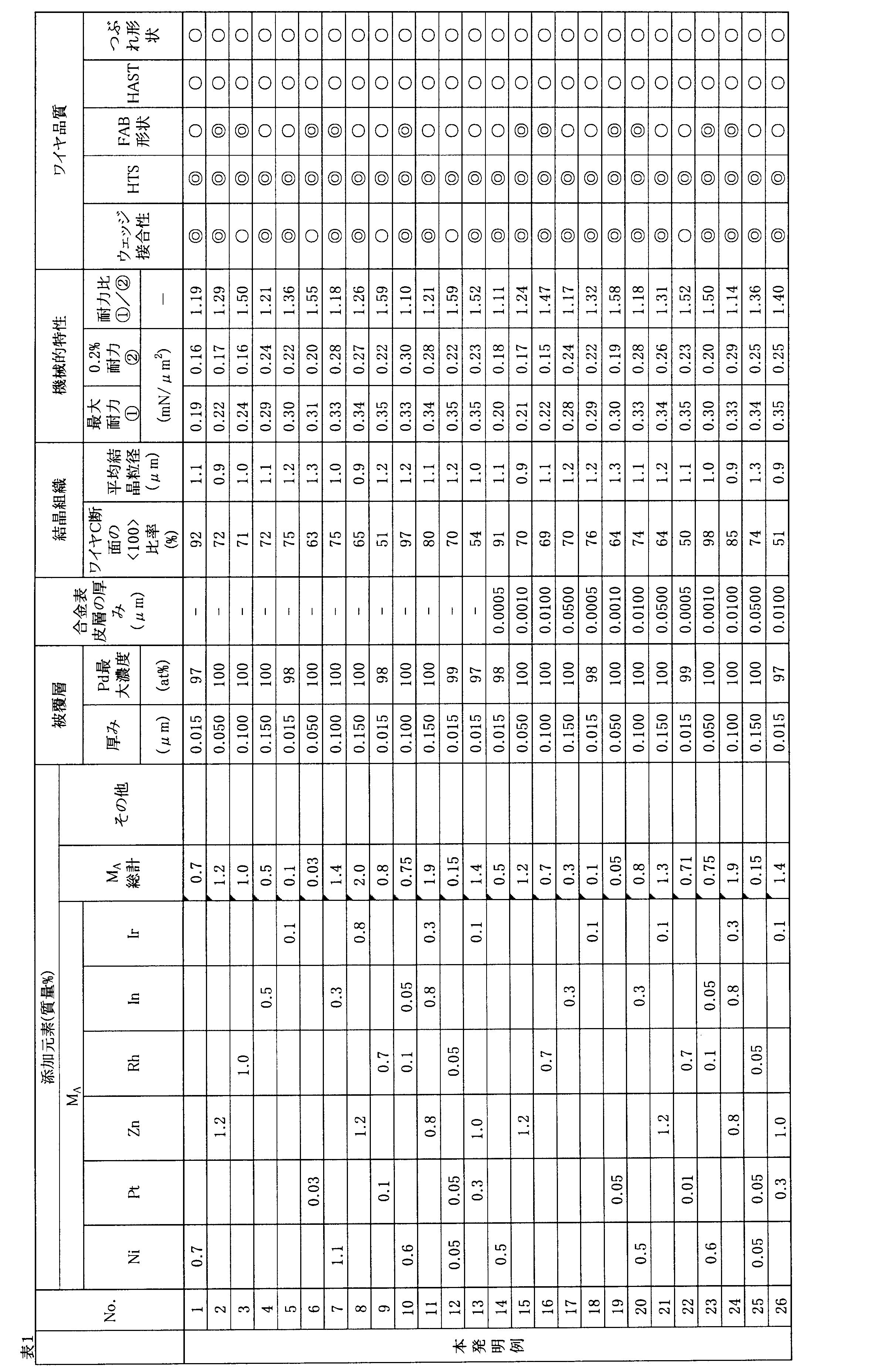


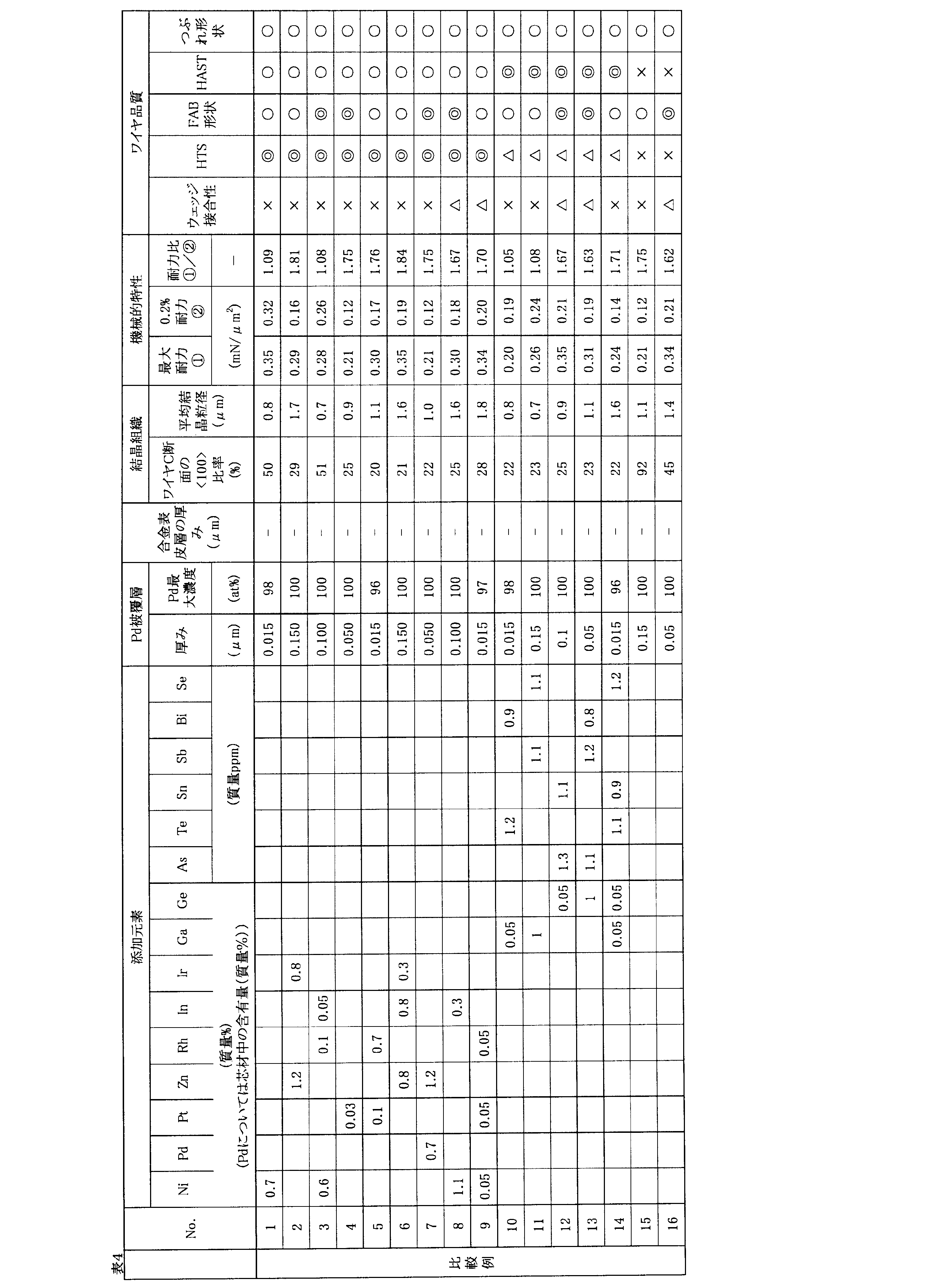
本発明例1~59に係るボンディングワイヤは、Cu合金芯材と、Cu合金芯材の表面に形成されたPd被覆層とを有し、Pd被覆層の厚さが好適範囲である0.015~0.150μmの範囲にあり、FAB形状がいずれも良好であった。また、これらのボンディングワイヤはNi、Zn、Rh、In、Ir、Ptから選ばれる少なくとも1種以上の元素を含み、ワイヤ全体に対する前記元素の濃度が合計で0.011~2質量%であることから、HTS評価によるボール接合部高温信頼性も良好であった。
(サンプル)
まずサンプルの作製方法について説明する。芯材の原材料となるCuは純度が99.99質量%以上で残部が不可避不純物から構成されるものを用いた。Ga、Ge、Ni、Ir、Pt、Pd、B、P、Mgは純度が99質量%以上で残部が不可避不純物から構成されるものを用いた。ワイヤ又は芯材の組成が目的のものとなるように、芯材への添加元素であるGa、Ge、Ni、Ir、Pt、Pd、B、P、Mgを調合する。Ga、Ge、Ni、Ir、Pt、Pd、B、P、Mgの添加に関しては、単体での調合も可能であるが、単体で高融点の元素や添加量が極微量である場合には、添加元素を含むCu母合金をあらかじめ作製しておいて目的の添加量となるように調合しても良い。
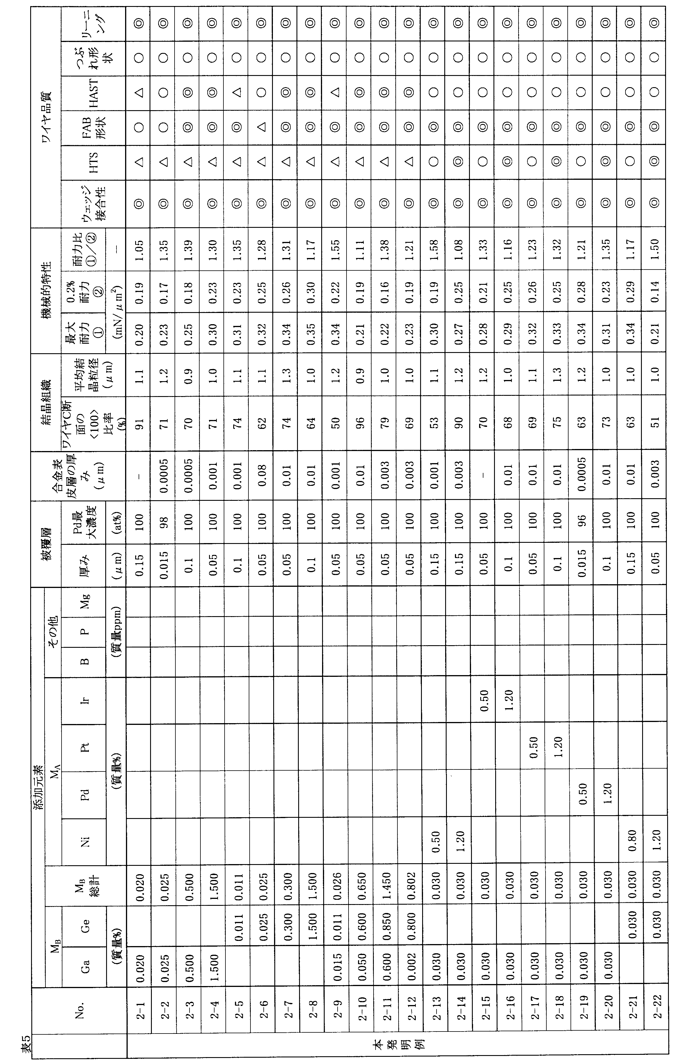
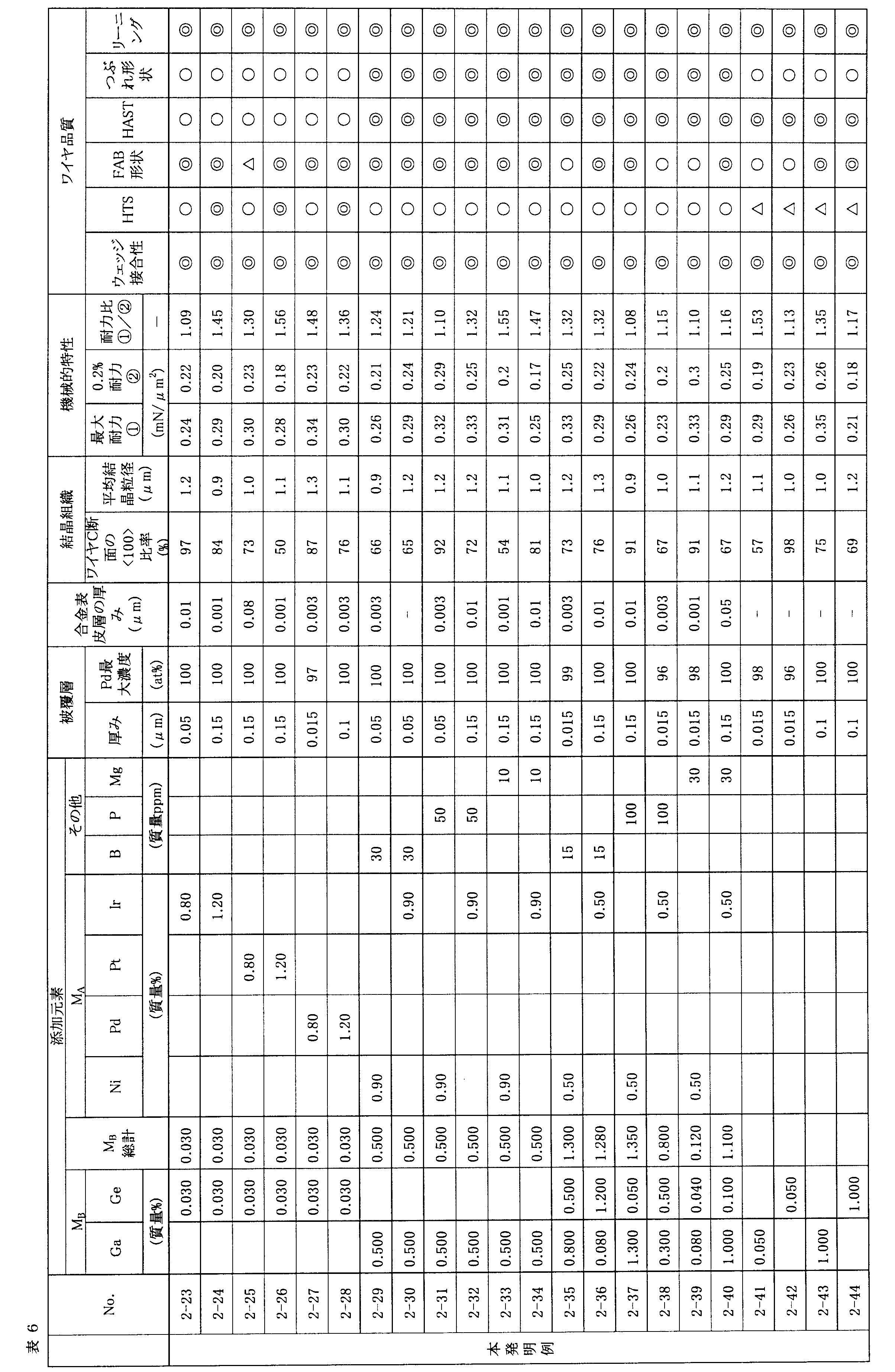
ワイヤ表面を観察面として、結晶組織の評価を行った。評価手法として、後方散乱電子線回折法(EBSD、Electron Backscattered Diffraction)を用いた。EBSD法は観察面の結晶方位を観察し、隣り合う測定点間での結晶方位の角度差を図示できるという特徴を有し、ボンディングワイヤのような細線であっても、比較的簡便ながら精度よく結晶方位を観察できる。
評価用のリードフレームに、ループ長5mm、ループ高さ0.5mmで100本ボンディングした。評価方法として、チップ水平方向からワイヤ直立部を観察し、ボール接合部の中心を通る垂線とワイヤ直立部との間隔が最大であるときの間隔(リーニング間隔)で評価した。リーニング間隔がワイヤ径よりも小さい場合にはリーニングは良好、大きい場合には直立部が傾斜しているためリーニングは不良であると判断した。100本のボンディングしたワイヤを光学顕微鏡で観察し、リーニング不良の本数を数えた。不良が7個以上発生した場合には問題があると判断し×印、不良が4~6個であれば実用可能であるがやや問題有りとして△印、不良が1~3個の場合は問題ないと判断し○印、不良が発生しなかった場合には優れていると判断し◎印とし、表5及び表6の「リーニング」の欄に表記した。
表5及び表6に示すように、本発明例2-1~2-44に係るボンディングワイヤは、Cu合金芯材と、Cu合金芯材の表面に形成されたPd被覆層とを有し、ボンディングワイヤがGa、Geから選ばれる1種以上の元素を含み、ワイヤ全体に対する前記元素の濃度が合計で0.011~1.5質量%である。これにより本発明例2-1~2-44に係るボンディングワイヤは、温度が130℃、相対湿度が85%の高温高湿環境下でのHAST試験でボール接合部信頼性が得られることを確認した。
(サンプル)
まずサンプルの作製方法について説明する。芯材の原材料となるCuは純度が99.99質量%以上で残部が不可避不純物から構成されるものを用いた。As、Te、Sn、Sb、Bi、Se、Ni、Zn、Rh、In、Ir、Pt、Ga、Ge、Pd、B、P、Mg、Ca、Laは純度が99質量%以上で残部が不可避不純物から構成されるものを用いた。ワイヤ又は芯材の組成が目的のものとなるように、芯材への添加元素であるAs、Te、Sn、Sb、Bi、Se、Ni、Zn、Rh、In、Ir、Pt、Ga、Ge、Pd、B、P、Mg、Ca、Laを調合する。As、Te、Sn、Sb、Bi、Se、Ni、Zn、Rh、In、Ir、Pt、Ga、Ge、Pd、B、P、Mg、Ca、Laの添加に関しては、単体での調合も可能であるが、単体で高融点の元素や添加量が極微量である場合には、添加元素を含むCu母合金をあらかじめ作製しておいて目的の添加量となるように調合しても良い。

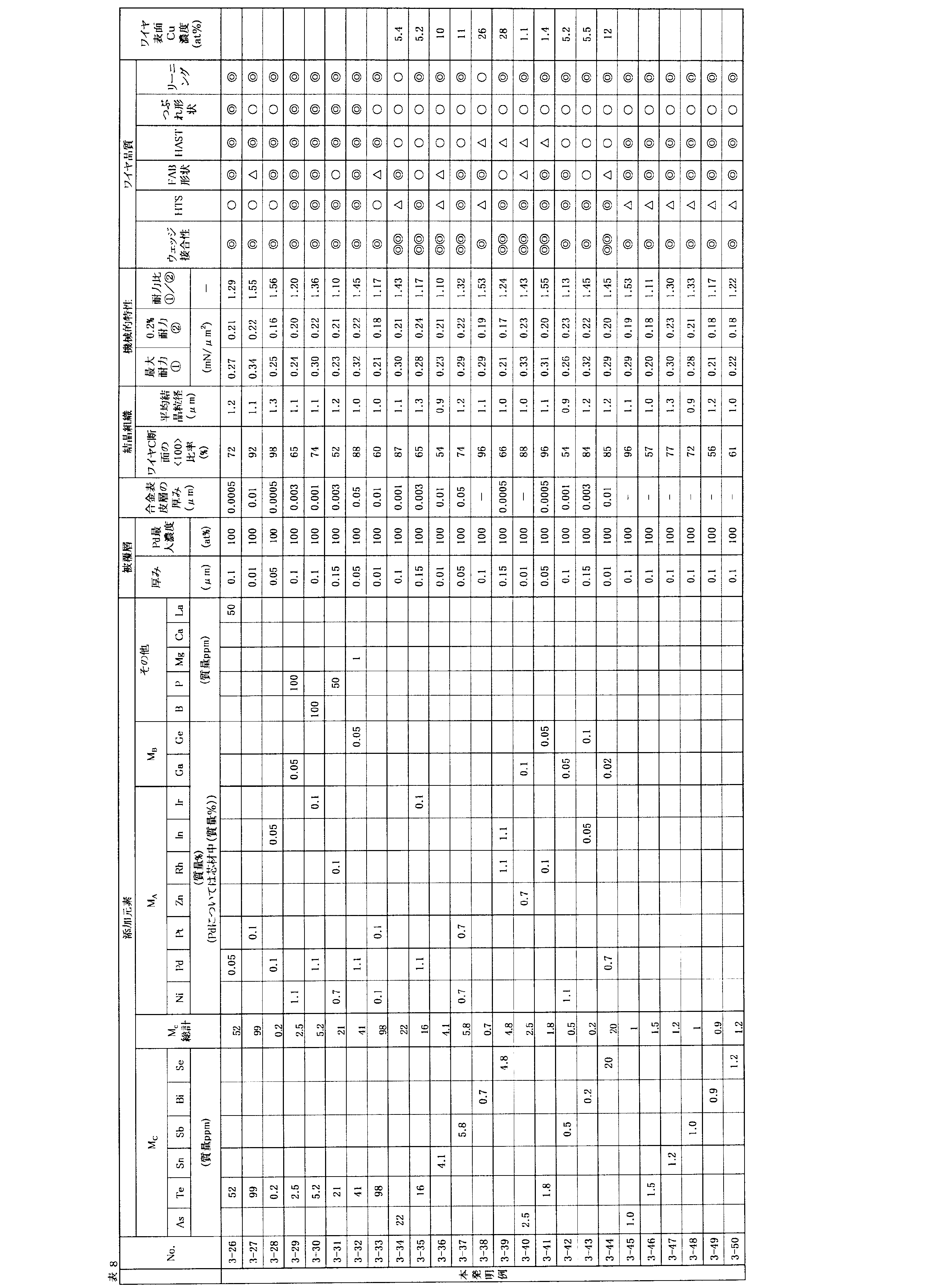
ワイヤ表面を観察面として、結晶組織の評価を行った。評価手法として、後方散乱電子線回折法(EBSD、Electron Backscattered Diffraction)を用いた。EBSD法は観察面の結晶方位を観察し、隣り合う測定点間での結晶方位の角度差を図示できるという特徴を有し、ボンディングワイヤのような細線であっても、比較的簡便ながら精度よく結晶方位を観察できる。
評価用のリードフレームに、ループ長5mm、ループ高さ0.5mmで100本ボンディングした。評価方法として、チップ水平方向からワイヤ直立部を観察し、ボール接合部の中心を通る垂線とワイヤ直立部との間隔が最大であるときの間隔(リーニング間隔)で評価した。リーニング間隔がワイヤ径よりも小さい場合にはリーニングは良好、大きい場合には直立部が傾斜しているためリーニングは不良であると判断した。100本のボンディングしたワイヤを光学顕微鏡で観察し、リーニング不良の本数を数えた。不良が7個以上発生した場合には問題があると判断し×印、不良が4~6個であれば実用可能であるがやや問題有りとして△印、不良が1~3個の場合は問題ないと判断し○印、不良が発生しなかった場合には優れていると判断し◎印とし、表7及び表8の「リーニング」の欄に表記した。
本発明例3-1~3-50に係るボンディングワイヤは、Cu合金芯材と、Cu合金芯材の表面に形成されたPd被覆層とを有し、ボンディングワイヤがAs、Te、Sn、Sb、Bi、Seから選ばれる少なくとも1種以上の元素を含み、ワイヤ全体に対する前記元素の濃度が合計で0.1~100質量ppmである。これにより本発明例3-1~3-50に係るボンディングワイヤは、温度が130℃、相対湿度が85%の高温高湿環境下でのHAST試験でボール接合部信頼性が得られることを確認した。
ボンディングワイヤの原材料として、Cu合金芯材を製造するために純度が99.99質量%以上のCu、添加元素としてNi、Pd、Pt、Au、P、B、Be、Fe、Mg、Ti、Zn、Ag、Siを用意し、被覆層形成用に純度が99.99質量%以上のPdを用意し、表皮合金層形成用に純度が99.99質量%以上のAuをそれぞれ用意した。Cuと添加元素原料を出発原料として秤量した後、これを高真空下で加熱して溶解することで直径10mm程度の銅合金インゴットを得た。その後、該インゴットを鍛造、圧延、伸線して直径500μmのCu合金ワイヤを作製した。次にCu合金ワイヤ表面にPd被覆層を1~3μm厚、被覆層の表面にAu表皮層を0.05~0.2μm厚になるように電解めっきで施し、複層ワイヤを得た。Pd被覆層、AuPd表皮合金層の最終的な厚みを表8に記載した。ここで、芯材と被覆層との境界はPd濃度が50原子%の位置とし、被覆層と表皮合金層との境界はAu濃度が10原子%の位置とした。その後、伸線速度が100~700m/min、ダイス減面率が8~30%で連続伸線加工を行い表8に記載した最終線径とした。表皮合金層の厚み、Au最大濃度、表面Cu濃度、被覆層の厚みは、伸線加工の間に熱処理を2回乃至3回実施することにより制御した。その時の条件は、ワイヤ直径が200~250μmにおいて温度500~700℃、速度10~70m/min、ワイヤ直径が70~100μmにおいて温度450~650℃、速度20~90m/min、最終線径が細い場合には、更にワイヤ直径が40~70μmにおいて温度300~500℃、速度30~100m/minであった。その後、最終線径で、表8の温度、速度30~120m/minで熱処理を実施した。また、表面までCuを拡散させるために1回の熱処理だけは、熱処理炉中の酸素濃度を0.2~0.7%と通常より高めに設定した。この熱処理はできれば最後の方に行ったほうが良く、その理由はCuが表面に出てから伸線加工を繰り返すとCuの酸化が起こり易くなるからである。それ以外の熱処理では、熱処理炉中の酸素濃度を0.2%未満にすることで、表皮合金層の過剰な酸化を抑えつつ、安定した厚さ、組成などを制御した。このようにして直径が15~25μmのボンディングワイヤを得た。
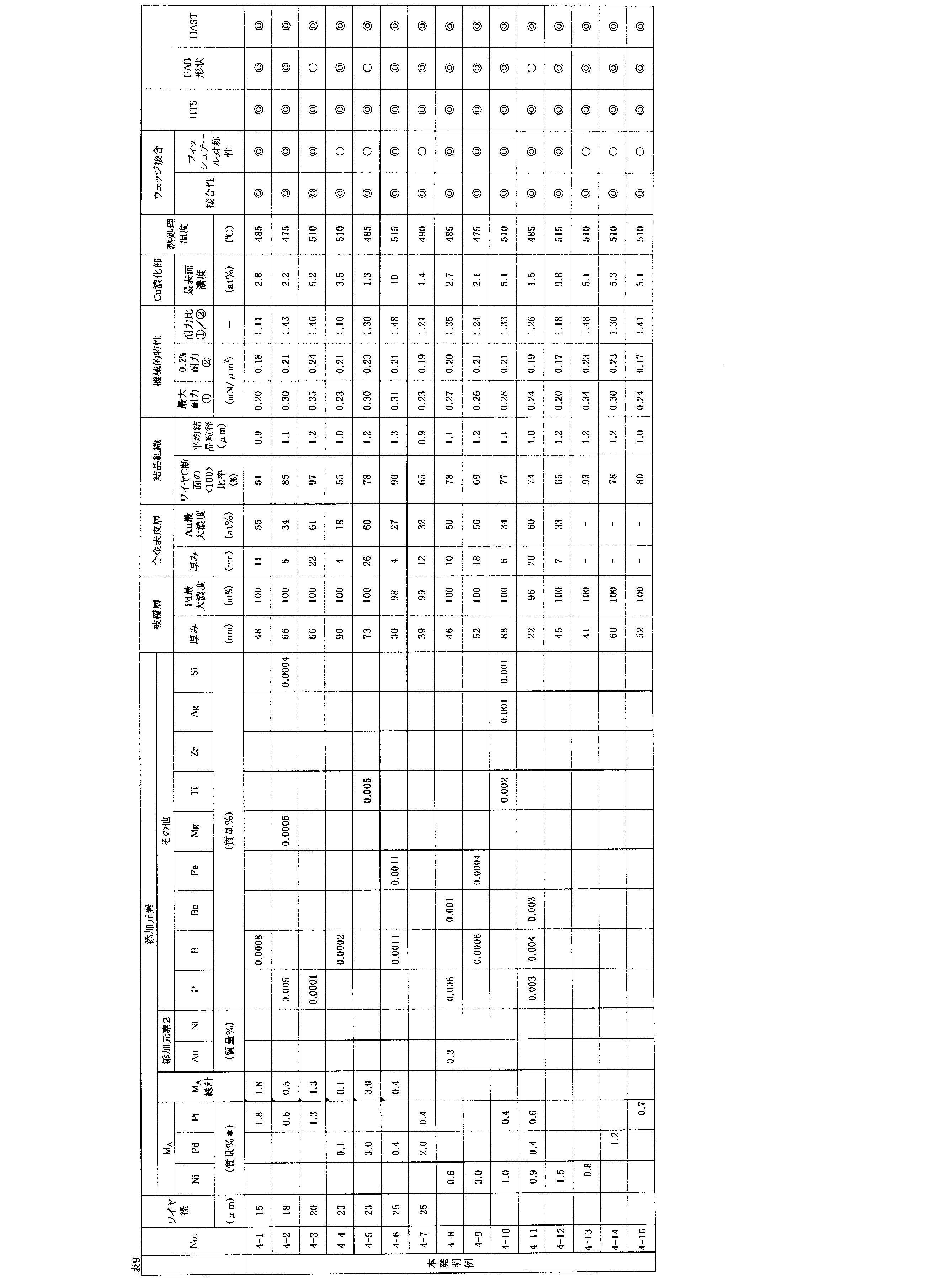
Claims (11)
- Cu合金芯材と、前記Cu合金芯材の表面に形成されたPd被覆層とを有する半導体装置用ボンディングワイヤにおいて、
前記ボンディングワイヤが、高温環境下における接続信頼性を付与する元素を含み、
前記ボンディングワイヤのワイヤ軸に垂直方向の芯材断面に対して結晶方位を測定した結果において、ワイヤ長手方向の結晶方位のうち、ワイヤ長手方向に対して角度差が15度以下である結晶方位<100>の方位比率が30%以上であり、
前記ボンディングワイヤのワイヤ軸に垂直方向の芯材断面における平均結晶粒径が、0.9~1.5μmであることを特徴とする半導体装置用ボンディングワイヤ。 - 下記(1)式で定義する耐力比が1.1~1.6であることを特徴とする請求項1記載の半導体装置用ボンディングワイヤ。
耐力比=最大耐力/0.2%耐力 (1) - 前記Pd被覆層の厚さが0.015~0.150μmであることを特徴とする請求項1又は2記載の半導体装置用ボンディングワイヤ。
- 前記Pd被覆層上にさらにAuとPdを含む合金表皮層を有することを特徴とする請求項1~3のいずれか1項記載の半導体装置用ボンディングワイヤ。
- 前記AuとPdを含む合金表皮層の厚さが0.050μm以下であることを特徴とする請求項4記載の半導体装置用ボンディングワイヤ。
- 前記ボンディングワイヤがNi、Zn、Rh、In、Ir、Ptから選ばれる少なくとも1種以上の元素を含み、ワイヤ全体に対する前記元素の濃度が総計で0.011~2質量%であることを特徴とする請求項1~5のいずれか1項記載の半導体装置用ボンディングワイヤ。
- 前記ボンディングワイヤがGa、Geから選ばれる1種以上の元素を含み、ワイヤ全体に対する前記元素の濃度が合計で0.011~1.5質量%であることを特徴とする請求項1~6のいずれか1項記載の半導体装置用ボンディングワイヤ。
- 前記ボンディングワイヤがAs、Te、Sn、Sb、Bi、Seから選ばれる1種以上の元素を含み、ワイヤ全体に対する前記元素の濃度が合計で0.1~100質量ppmであり、Sn≦10質量ppm、Sb≦10質量ppm、Bi≦1質量ppmであることを特徴とする請求項1~7のいずれか1項記載の半導体装置用ボンディングワイヤ。
- 前記ボンディングワイヤがさらにB、P、Mg、Ca、Laから選ばれる少なくとも1種以上の元素を含み、ワイヤ全体に対する前記元素の濃度がそれぞれ1~200質量ppmであることを特徴とする請求項1~8のいずれか1項記載の半導体装置用ボンディングワイヤ。
- 前記ボンディングワイヤの最表面にCuが存在することを特徴とする請求項1~9のいずれか1項記載の半導体装置用ボンディングワイヤ。
- Cu合金芯材が、元素周期表第10族の金属元素を総計で0.1~3.0質量%含有し、ワイヤ最表面におけるCu濃度が1原子%以上であることを特徴とする請求項1~10のいずれか1項記載の半導体装置用ボンディングワイヤ。
Priority Applications (11)
| Application Number | Priority Date | Filing Date | Title |
|---|---|---|---|
| DE112016000133.9T DE112016000133B4 (de) | 2015-06-15 | 2016-05-19 | Bonddraht für Halbleitervorrichtung |
| US15/515,508 US10414002B2 (en) | 2015-06-15 | 2016-05-19 | Bonding wire for semiconductor device |
| EP18154972.6A EP3349246B1 (en) | 2015-06-15 | 2016-05-19 | Bonding wire for semiconductor device |
| KR1020177005522A KR101777995B1 (ko) | 2015-06-15 | 2016-05-19 | 반도체 장치용 본딩 와이어 |
| EP16811374.4A EP3282473B1 (en) | 2015-06-15 | 2016-05-19 | Bonding wire for semiconductor device |
| CN201680002657.9A CN106688086A (zh) | 2015-06-15 | 2016-05-19 | 半导体装置用接合线 |
| KR1020187034354A KR20180129987A (ko) | 2015-06-15 | 2016-05-19 | 반도체 장치용 본딩 와이어 |
| KR1020177024954A KR101925236B1 (ko) | 2015-06-15 | 2016-05-19 | 반도체 장치용 본딩 와이어 |
| CN201711344468.2A CN107962313B (zh) | 2015-06-15 | 2016-05-19 | 半导体装置用接合线 |
| JP2016533746A JP5985127B1 (ja) | 2015-06-15 | 2016-05-19 | 半導体装置用ボンディングワイヤ |
| US15/851,554 US10610976B2 (en) | 2015-06-15 | 2017-12-21 | Bonding wire for semiconductor device |
Applications Claiming Priority (4)
| Application Number | Priority Date | Filing Date | Title |
|---|---|---|---|
| JP2015-120509 | 2015-06-15 | ||
| JP2015120509 | 2015-06-15 | ||
| JPPCT/JP2015/070861 | 2015-07-22 | ||
| PCT/JP2015/070861 WO2016203659A1 (ja) | 2015-06-15 | 2015-07-22 | 半導体装置用ボンディングワイヤ |
Related Child Applications (2)
| Application Number | Title | Priority Date | Filing Date |
|---|---|---|---|
| US15/515,508 A-371-Of-International US10414002B2 (en) | 2015-06-15 | 2016-05-19 | Bonding wire for semiconductor device |
| US15/851,554 Continuation US10610976B2 (en) | 2015-06-15 | 2017-12-21 | Bonding wire for semiconductor device |
Publications (1)
| Publication Number | Publication Date |
|---|---|
| WO2016203899A1 true WO2016203899A1 (ja) | 2016-12-22 |
Family
ID=55808270
Family Applications (1)
| Application Number | Title | Priority Date | Filing Date |
|---|---|---|---|
| PCT/JP2016/064926 Ceased WO2016203899A1 (ja) | 2015-06-15 | 2016-05-19 | 半導体装置用ボンディングワイヤ |
Country Status (3)
| Country | Link |
|---|---|
| JP (1) | JP5912008B1 (ja) |
| KR (1) | KR101670209B1 (ja) |
| WO (1) | WO2016203899A1 (ja) |
Cited By (4)
| Publication number | Priority date | Publication date | Assignee | Title |
|---|---|---|---|---|
| CN115836384A (zh) * | 2021-06-25 | 2023-03-21 | 日铁新材料股份有限公司 | 半导体装置用接合线 |
| CN116568835A (zh) * | 2021-12-07 | 2023-08-08 | 古河电气工业株式会社 | 铜系线材及半导体器件 |
| EP4289986A4 (en) * | 2021-02-05 | 2025-01-15 | Nippon Micrometal Corporation | AL-BOND WIRE FOR SEMICONDUCTOR COMPONENTS |
| US12300658B2 (en) | 2016-06-20 | 2025-05-13 | Nippon Micrometal Corporation | Copper alloy bonding wire for semiconductor devices |
Families Citing this family (5)
| Publication number | Priority date | Publication date | Assignee | Title |
|---|---|---|---|---|
| US10137534B2 (en) | 2015-06-15 | 2018-11-27 | Nippon Micrometal Corporation | Bonding wire for semiconductor device |
| WO2017013796A1 (ja) | 2015-07-23 | 2017-01-26 | 日鉄住金マイクロメタル株式会社 | 半導体装置用ボンディングワイヤ |
| JP6452661B2 (ja) * | 2016-11-11 | 2019-01-16 | 日鉄マイクロメタル株式会社 | 半導体装置用ボンディングワイヤ |
| WO2019130570A1 (ja) * | 2017-12-28 | 2019-07-04 | 日鉄マイクロメタル株式会社 | 半導体装置用ボンディングワイヤ |
| WO2023276943A1 (ja) * | 2021-06-30 | 2023-01-05 | ローム株式会社 | 半導体装置 |
Citations (2)
| Publication number | Priority date | Publication date | Assignee | Title |
|---|---|---|---|---|
| WO2009072525A1 (ja) * | 2007-12-03 | 2009-06-11 | Nippon Steel Materials Co., Ltd. | 半導体装置用ボンディングワイヤ |
| JP2009140953A (ja) * | 2007-12-03 | 2009-06-25 | Nippon Steel Materials Co Ltd | 半導体装置用ボンディングワイヤ |
Family Cites Families (5)
| Publication number | Priority date | Publication date | Assignee | Title |
|---|---|---|---|---|
| JPS6148543A (ja) | 1984-08-10 | 1986-03-10 | Sumitomo Electric Ind Ltd | 半導体素子結線用銅合金線 |
| JP2005167020A (ja) | 2003-12-03 | 2005-06-23 | Sumitomo Electric Ind Ltd | ボンディングワイヤーおよびそれを使用した集積回路デバイス |
| JP4885117B2 (ja) * | 2007-12-03 | 2012-02-29 | 新日鉄マテリアルズ株式会社 | 半導体装置用ボンディングワイヤ |
| JP4919364B2 (ja) | 2010-08-11 | 2012-04-18 | 田中電子工業株式会社 | ボールボンディング用金被覆銅ワイヤ |
| JP5556577B2 (ja) * | 2010-10-20 | 2014-07-23 | 日立金属株式会社 | 銅ボンディングワイヤ |
-
2015
- 2015-07-22 JP JP2015552702A patent/JP5912008B1/ja active Active
- 2015-07-22 KR KR1020167010922A patent/KR101670209B1/ko active Active
-
2016
- 2016-05-19 WO PCT/JP2016/064926 patent/WO2016203899A1/ja not_active Ceased
Patent Citations (2)
| Publication number | Priority date | Publication date | Assignee | Title |
|---|---|---|---|---|
| WO2009072525A1 (ja) * | 2007-12-03 | 2009-06-11 | Nippon Steel Materials Co., Ltd. | 半導体装置用ボンディングワイヤ |
| JP2009140953A (ja) * | 2007-12-03 | 2009-06-25 | Nippon Steel Materials Co Ltd | 半導体装置用ボンディングワイヤ |
Cited By (6)
| Publication number | Priority date | Publication date | Assignee | Title |
|---|---|---|---|---|
| US12300658B2 (en) | 2016-06-20 | 2025-05-13 | Nippon Micrometal Corporation | Copper alloy bonding wire for semiconductor devices |
| EP4289986A4 (en) * | 2021-02-05 | 2025-01-15 | Nippon Micrometal Corporation | AL-BOND WIRE FOR SEMICONDUCTOR COMPONENTS |
| CN115836384A (zh) * | 2021-06-25 | 2023-03-21 | 日铁新材料股份有限公司 | 半导体装置用接合线 |
| US11929343B2 (en) | 2021-06-25 | 2024-03-12 | Nippon Micrometal Corporation | Bonding wire for semiconductor devices |
| CN115836384B (zh) * | 2021-06-25 | 2024-06-11 | 日铁新材料股份有限公司 | 半导体装置用接合线 |
| CN116568835A (zh) * | 2021-12-07 | 2023-08-08 | 古河电气工业株式会社 | 铜系线材及半导体器件 |
Also Published As
| Publication number | Publication date |
|---|---|
| JPWO2016203659A1 (ja) | 2017-06-22 |
| JP5912008B1 (ja) | 2016-04-27 |
| KR101670209B1 (ko) | 2016-10-27 |
Similar Documents
| Publication | Publication Date | Title |
|---|---|---|
| JP6254649B2 (ja) | 半導体装置用ボンディングワイヤ | |
| JP6420015B2 (ja) | 半導体装置用ボンディングワイヤ | |
| JP6605418B2 (ja) | 半導体装置用ボンディングワイヤ | |
| JP5985127B1 (ja) | 半導体装置用ボンディングワイヤ | |
| JP5912008B1 (ja) | 半導体装置用ボンディングワイヤ | |
| WO2016135993A1 (ja) | 半導体装置用ボンディングワイヤ | |
| WO2016189758A1 (ja) | 半導体装置用ボンディングワイヤ | |
| JP5937770B1 (ja) | 半導体装置用ボンディングワイヤ |
Legal Events
| Date | Code | Title | Description |
|---|---|---|---|
| ENP | Entry into the national phase |
Ref document number: 2016533746 Country of ref document: JP Kind code of ref document: A |
|
| 121 | Ep: the epo has been informed by wipo that ep was designated in this application |
Ref document number: 16811374 Country of ref document: EP Kind code of ref document: A1 |
|
| ENP | Entry into the national phase |
Ref document number: 20177005522 Country of ref document: KR Kind code of ref document: A |
|
| WWE | Wipo information: entry into national phase |
Ref document number: 15515508 Country of ref document: US |
|
| WWE | Wipo information: entry into national phase |
Ref document number: 112016000133 Country of ref document: DE |