WO2016204168A1 - 光子検出装置及び光子検出方法 - Google Patents
光子検出装置及び光子検出方法 Download PDFInfo
- Publication number
- WO2016204168A1 WO2016204168A1 PCT/JP2016/067747 JP2016067747W WO2016204168A1 WO 2016204168 A1 WO2016204168 A1 WO 2016204168A1 JP 2016067747 W JP2016067747 W JP 2016067747W WO 2016204168 A1 WO2016204168 A1 WO 2016204168A1
- Authority
- WO
- WIPO (PCT)
- Prior art keywords
- strip line
- photon detection
- superconducting strip
- photon
- superconducting
- Prior art date
- Legal status (The legal status is an assumption and is not a legal conclusion. Google has not performed a legal analysis and makes no representation as to the accuracy of the status listed.)
- Ceased
Links
Images




Classifications
-
- G—PHYSICS
- G01—MEASURING; TESTING
- G01J—MEASUREMENT OF INTENSITY, VELOCITY, SPECTRAL CONTENT, POLARISATION, PHASE OR PULSE CHARACTERISTICS OF INFRARED, VISIBLE OR ULTRAVIOLET LIGHT; COLORIMETRY; RADIATION PYROMETRY
- G01J1/00—Photometry, e.g. photographic exposure meter
- G01J1/42—Photometry, e.g. photographic exposure meter using electric radiation detectors
- G01J1/44—Electric circuits
-
- G—PHYSICS
- G01—MEASURING; TESTING
- G01J—MEASUREMENT OF INTENSITY, VELOCITY, SPECTRAL CONTENT, POLARISATION, PHASE OR PULSE CHARACTERISTICS OF INFRARED, VISIBLE OR ULTRAVIOLET LIGHT; COLORIMETRY; RADIATION PYROMETRY
- G01J1/00—Photometry, e.g. photographic exposure meter
- G01J1/02—Details
-
- H—ELECTRICITY
- H10—SEMICONDUCTOR DEVICES; ELECTRIC SOLID-STATE DEVICES NOT OTHERWISE PROVIDED FOR
- H10N—ELECTRIC SOLID-STATE DEVICES NOT OTHERWISE PROVIDED FOR
- H10N60/00—Superconducting devices
-
- H—ELECTRICITY
- H10—SEMICONDUCTOR DEVICES; ELECTRIC SOLID-STATE DEVICES NOT OTHERWISE PROVIDED FOR
- H10N—ELECTRIC SOLID-STATE DEVICES NOT OTHERWISE PROVIDED FOR
- H10N60/00—Superconducting devices
- H10N60/10—Junction-based devices
-
- H—ELECTRICITY
- H10—SEMICONDUCTOR DEVICES; ELECTRIC SOLID-STATE DEVICES NOT OTHERWISE PROVIDED FOR
- H10N—ELECTRIC SOLID-STATE DEVICES NOT OTHERWISE PROVIDED FOR
- H10N60/00—Superconducting devices
- H10N60/80—Constructional details
- H10N60/805—Constructional details for Josephson-effect devices
-
- H—ELECTRICITY
- H10—SEMICONDUCTOR DEVICES; ELECTRIC SOLID-STATE DEVICES NOT OTHERWISE PROVIDED FOR
- H10N—ELECTRIC SOLID-STATE DEVICES NOT OTHERWISE PROVIDED FOR
- H10N60/00—Superconducting devices
- H10N60/80—Constructional details
- H10N60/84—Switching means for devices switchable between superconducting and normal states
-
- G—PHYSICS
- G01—MEASURING; TESTING
- G01J—MEASUREMENT OF INTENSITY, VELOCITY, SPECTRAL CONTENT, POLARISATION, PHASE OR PULSE CHARACTERISTICS OF INFRARED, VISIBLE OR ULTRAVIOLET LIGHT; COLORIMETRY; RADIATION PYROMETRY
- G01J1/00—Photometry, e.g. photographic exposure meter
- G01J1/42—Photometry, e.g. photographic exposure meter using electric radiation detectors
- G01J1/44—Electric circuits
- G01J2001/4413—Type
- G01J2001/442—Single-photon detection or photon counting
-
- G—PHYSICS
- G01—MEASURING; TESTING
- G01J—MEASUREMENT OF INTENSITY, VELOCITY, SPECTRAL CONTENT, POLARISATION, PHASE OR PULSE CHARACTERISTICS OF INFRARED, VISIBLE OR ULTRAVIOLET LIGHT; COLORIMETRY; RADIATION PYROMETRY
- G01J1/00—Photometry, e.g. photographic exposure meter
- G01J1/42—Photometry, e.g. photographic exposure meter using electric radiation detectors
- G01J1/44—Electric circuits
- G01J2001/4446—Type of detector
-
- H—ELECTRICITY
- H04—ELECTRIC COMMUNICATION TECHNIQUE
- H04L—TRANSMISSION OF DIGITAL INFORMATION, e.g. TELEGRAPHIC COMMUNICATION
- H04L9/00—Cryptographic mechanisms or cryptographic arrangements for secret or secure communications; Network security protocols
- H04L9/08—Key distribution or management, e.g. generation, sharing or updating, of cryptographic keys or passwords
- H04L9/0816—Key establishment, i.e. cryptographic processes or cryptographic protocols whereby a shared secret becomes available to two or more parties, for subsequent use
- H04L9/0852—Quantum cryptography
Definitions
- the present invention relates to a photon detection device and a photon detection method using a superconducting strip line.
- InGaAs avalanche photodiodes have been widely used for photon detection in the communication wavelength band (1,550 nm), but there are problems of generation of afterpulses and dark counts. These problems are factors that increase the error rate of key generation, but are difficult to avoid due to the operating principle of APD.
- SSPD superconducting strip photon detector
- the SSPD is a photon detection device composed of a superconducting strip line having a thickness of several nanometers and a width of several tens to several hundreds of nanometers, and is operated by always passing a bias current through the superconducting strip line.
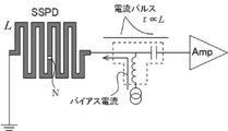
- a photon is incident on a superconducting strip line in a state where a bias current flows, a complete normal conducting region is formed in the width direction of the superconducting strip line (see N in FIG. 1A). Then, the bias current cannot flow in the forward direction, and a current pulse is output to the measurement system. In SSPD, this current pulse is used as a photon detection signal.
- FIG. 1B is a diagram showing the bias current dependency of the quantum efficiency and the bias current dependency of the dark count rate.
- the current pulse in order to use the current pulse as a photon detection principle, it is necessary to use a low noise amplifier for amplifying the current pulse shown in FIG. Low noise amplifiers have the problem of adversely affecting the jitter of the detection system.
- the fall time ⁇ of the current pulse which is the principle of photon detection, is limited by the magnitude of the inductance L of the superconducting strip line.
- the inductance L is inversely proportional to the cross-sectional area of the entire length of the superconducting strip line, and in order to reduce the size of the inductance L, it is necessary to increase the cross-sectional area of the superconducting strip line.
- the cross-sectional area of the superconducting strip line must be small, and if it is large, the formation of the normal conduction region at the time of photon incidence becomes incomplete and the sensitivity is lowered. Therefore, the inductance L must be increased. Therefore, there is a problem that the current pulse falls slowly and the fall time ⁇ becomes long, and the response time constant of the system becomes as large as several tens ns, and the count rate can be obtained only about several hundred MHz.
- the present invention solves the above-mentioned problems in the prior art, is practical, has no after-pulse, can perform photon detection with suppressed dark count generation, and can obtain a high count rate with low jitter.
- An object is to provide a detection device and a photon detection method.
- Means for solving the problems are as follows. That is, ⁇ 1> A long plate-like superconducting strip line whose plate surface is a photon detection surface, a photon detection unit having bias current supply means for supplying a bias current to the superconducting strip line, and the superconducting strip at the time of photon detection
- a photon detection device comprising: a single magnetic flux quantum comparator circuit capable of detecting a magnetic flux scattered from a line.
- a single magnetic flux quantum comparator circuit has at least a Josephson junction wiring having a Josephson junction in the wiring, and a superconducting wiring for electrically connecting the Josephson junction wiring and the superconducting strip line.
- the photon detection device wherein a superconducting loop capable of detecting a magnetic flux is configured by the superconducting strip line, the superconducting wiring, and the Josephson junction wiring.
- the bias current supply means is a means for supplying a bias current having a value of 60% to 85% to the superconductive strip line with respect to the critical current value of the superconductive strip line.
- the photon detection device according to any one of the above.
- ⁇ 4> The photon detection device according to any one of ⁇ 1> to ⁇ 3>, wherein a superconducting strip line is disposed on an optical waveguide through which a photon to be detected is guided.
- a plurality of superconducting strip lines are arranged along the optical waveguide direction of the optical waveguide, and a plurality of photon detectors and single flux quantum comparator circuits are arranged corresponding to each of the superconducting strip lines.
- the photon detection device according to any one of ⁇ 4>, wherein an integrated input circuit into which output signals output from the single magnetic flux quantum comparator circuits are input in an integrated manner is arranged.
- ⁇ 6> Further, the time difference between the input time of the reference time signal and the input time of the output signal output from the single magnetic flux quantum comparator circuit or the integrated input circuit when the magnetic flux is detected is measured, and the output signal is calculated from the time difference.
- the photon detection device according to any one of ⁇ 1> to ⁇ 5>, further including a time digital converter that converts the data into digital data.
- a photon detection method wherein the photon is detected by detecting a magnetic flux scattered from the superconducting strip line by the incidence of the photon by a single magnetic flux quantum comparator circuit.
- the above-described problems in the prior art can be solved, practical, free of afterpulses, photon detection can be performed while suppressing the occurrence of dark count, and low jitter and high counting can be achieved. It is possible to provide a photon detection device and a photon detection method capable of obtaining a rate.
- the photon detection device 10 mainly includes a superconducting strip line 1 and a Josephson Transmission Line (JTL) circuit 4 as a single flux quantum (SFQ) circuit.
- JTL Josephson Transmission Line
- Superconducting strip line 1 is a long plate-like member whose plate surface is a photon detection surface.
- the superconducting strip wire 1 is not particularly limited and can be appropriately selected from known ones.
- the shape of the superconducting strip line 1 is not particularly limited, but here, the magnetic flux eliminated from the superconducting strip line 1 is eliminated in a direction perpendicular to the length direction of the line, and the magnetic flux in the JTL circuit 4 is obtained.
- the shape is linear. However, even in the case of a linear shape, as long as the JTL circuit 4 can detect the magnetic flux excluded outside the line when a photon is incident, it does not prevent the addition of a portion other than the linear portion in addition to the linear portion.
- the line width of the superconducting strip line 1 is not particularly limited and is generally about 10 nm to 200 nm, and the thickness is also not particularly limited and is about 1 nm to 20 nm.
- the length of the superconducting strip line 1 is not particularly limited, but is preferably 1 ⁇ m or more and less than 10 ⁇ m, and more preferably 2 ⁇ m to 5 ⁇ m. When the length is less than 1 ⁇ m, the photon absorptance is low, and when it is 10 ⁇ m or more, the current detection sensitivity in the JTL circuit 4 may be lowered.
- Bias current is supplied to the superconducting strip line 1.
- the bias current supply means for supplying the bias current is not particularly limited, and examples thereof include a means for supplying a bias current having an appropriate magnitude via the current source 2.
- the superconducting strip line 1 and the bias current supply means constitute a photon detector.
- an electrical connection is made between the Josephson junction wiring 5 a that constitutes the first stage of the JTL circuit 4 and has a Josephson junction (a junction indicated by x in FIG. 2) and the superconducting strip line 1.
- a superconducting loop 3 capable of detecting a magnetic flux is constituted by the superconducting strip line 1, the superconducting wiring 3, and the Josephson junction wiring 5a. That is, in the photon detection device 10, the superconducting wiring 3 and the Josephson junction wiring 5a constitute an SFQ comparator circuit.
- the superconducting wiring 3 is not particularly limited, and a capacitor having a relatively small capacitor may be employed.
- the superconducting strip line 1 and the Josephson junction wiring 5a are connected by a common ground to constitute the superconducting loop.
- the JTL circuit 4 is not particularly limited, and can have the same configuration as a known JTL circuit.
- Josephson junctions include a mode in which a thin insulating film is sandwiched between two superconducting materials, and a mode in which a part of the superconducting material is processed to be thinner than other portions (weak coupling). Includes junctions that produce the Son effect.
- the length direction of the linear superconducting strip line 1 on the extension in the width direction of the superconducting strip line 1 is used.
- the Josephson junction wiring 5a is preferably arranged in the vicinity of the superconducting strip line 1, and the distance between the superconducting strip line 1 and the Josephson junction wiring 5a is the shortest. The distance is preferably 1 ⁇ m to 10 ⁇ m.
- the superconducting wiring 3 is not provided, the superconducting strip line 1 and the JTL circuit 4 are configured separately, and the superconducting loop in the JTL circuit 4 scatters from the superconducting strip line 1. It can also comprise so that the magnetic flux to be detected may be detected.
- the JTL circuit 4 constitutes an SFQ comparator circuit.
- the superconducting strip line 1 including the superconducting wiring 3 and discharging the magnetic flux and the magnetic flux Is formed as a monolithic body with a fixed arrangement relationship of each part, so that photons can be detected stably and is more practical.
- the superconducting strip line 1 itself constitutes the superconducting loop, it is easy to catch the magnetic flux, and the magnetic flux is detected with higher detection sensitivity than the configuration of detecting the magnetic flux scattered from outside the superconducting loop in the modified example. Can be more practical.
- the wiring that constitutes the photon detection unit including the superconducting strip line 1 and the wiring that constitutes the comparator circuit are made of the same superconducting material, the production efficiency is improved. Can be improved and microfabrication can be facilitated, which is more practical.
- the JTL circuit 4 is connected to the SFQ logic circuit 6.
- the SFQ logic circuit 6 is not particularly limited. For example, the time difference between the input time of the reference time signal and the input time of the output signal output from the SFQ comparator circuit (JTL circuit 4) when the magnetic flux is detected is measured.
- a time-to-digital converter (TDC) that converts the output signal into digital data from the time difference can be used.
- the TDC is not particularly limited and may be appropriately selected from known ones. However, for operation in a cryogenic environment, the TDC is configured by an SFQ circuit described in the following reference developed by the present inventors. SFQ-TDC is preferred.
- the SFQ-TDC can perform signal processing with a timing jitter of 2.5 picoseconds or less.
- the signal converted into digital data by the TDC is transmitted to a device in a room temperature environment outside the apparatus.
- a cable capable of broadband transmission is also a good conductor of heat, so it is difficult to transmit an ultrafast pulse to a room temperature environment.
- a cable for transmitting a signal converted into digital data may be a MHz band transmission, and can transmit the signal to a room temperature environment.
- the photon detection apparatus 10 since the photon detection apparatus 10 includes a superconducting operation, the photon detection apparatus 10 is used by being accommodated in a refrigerator or the like (not shown).
- FIG. 3A is a diagram illustrating a result of simulating temporal variation of the superconducting order parameter when a photon is incident on the superconducting strip line. As shown in FIG. 3A, it can be seen that the superconducting order parameter oscillates with a delay of about 5 picoseconds after the incidence of the photon.
- FIG. 3B is an explanatory diagram showing the dissociation state of the magnetic flux-antimagnetic flux pair.
- the magnetic flux-antimagnetic flux pair generated in the superconducting strip line 1 due to the oscillation of the superconducting order parameter receives the Lorentz force by the bias current flowing through the superconducting strip line 1 and dissociates into the magnetic flux-antimagnetic flux pair.
- the magnetic flux-antimagnetic flux pair is eliminated from the line 1 in the direction orthogonal to the direction in which the bias current flows, that is, in the width direction of the superconducting strip line 1, and these are scattered from the superconducting strip line 1.
- a complete normal conduction region is formed in the width direction of the superconducting strip line 1.
- a current pulse is output by forming a complete normal conduction region in the width direction of such a superconducting strip line 1, in other words, the superconducting strip line 1. This means that it is necessary to pass a sufficiently large bias current to near the critical current.
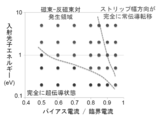
- FIG. 3C shows the relationship between the phenomenon that occurs in the superconducting strip line when a photon is incident and the bias current.
- the width direction of the superconducting strip line 1 is in a completely normal state with respect to incidence of photons (energy about 1 eV) in the communication wavelength band (1,550 nm).
- a bias current having a value of 90% or more with respect to the critical current value is required (the upper right region in the figure).
- the width direction of the superconducting strip line 1 does not become a complete normal conduction state, Magnetic flux pairs can be generated.
- a photon in the communication wavelength band is dark-count free by passing a bias current of 60% to 85% of the critical current value of the superconducting strip line 1 to the superconducting strip line 1. Can be detected.
- the magnetic flux scattered from the superconducting strip line 1 is captured by the superconducting loop composed of the superconducting strip line 1, the superconducting wiring 3, and the Josephson junction wiring 5a as a single flux quantum.
- a pulsed loop current is generated.
- a bias current is made to flow through the Josephson junction wiring 5a that forms the first stage of the JTL circuit 4 and has a Josephson junction (junction indicated by x in FIG. 2) in the wiring, the sum of the loop current and the bias current is obtained.
- the Josephson junction Temporarily exceeds the critical current value of the Josephson junction of the Josephson junction wiring 5a, the Josephson junction transitions to normal conduction, and an SFQ pulse is generated on the Josephson junction wiring 5a.
- the SFQ pulse flowing through the Josephson junction 5a generates a current on the right side (output side) of the circuit.
- the current generated on the right side (output side) of the circuit causes a bias current to flow in the Josephson junction wiring 5b that forms the next stage of the JTL circuit 4 and has a Josephson junction (a junction indicated by x in FIG. 2) in the wiring.
- the response time constant of the generated SFQ pulse can be set to several picoseconds even with a general JTL circuit.
- the SFQ pulse propagating through the JTL circuit 4 is output to the SFQ logic circuit 6, converted into digital data, and transmitted to a room temperature environment through an appropriate cable. If the SFQ-TDC is used as the SFQ logic circuit 6, signal processing can be performed with a timing jitter of 2.5 picoseconds or less.
- the Josephson junction wiring 5a constituting the first stage of the JTL circuit 4 has been described as a constituent member of the comparator circuit.
- the JTL circuit 4 itself is generated on the Josephson junction wiring 5a.
- the means for transmitting the SFQ pulse which can be considered separately from the comparator circuit. Therefore, as a further modification, in addition to the photon detector including the superconducting strip line 1, the superconducting wiring 3, and the Josephson junction wiring 5a, the Josephson junction wiring 5a is not provided.
- a photon detection device may be constituted by a known bias current supply means for supplying a bias current to the comparator circuit and a comparator circuit constituted by a known detection means for detecting an SFQ pulse generated on the Josephson junction wiring 5a. .
- the superconducting strip line 1 is used for photon detection, there is no after-pulse like APD.
- the superconducting strip line 1 since it is possible to operate with a lower bias current / critical current ratio than SSPD, it is possible to perform photon detection with suppressed dark count.
- a weak current pulse in the superconducting strip line 1 is not used as a photon detection principle, it is not necessary to use a low noise amplifier (see FIG. 1A) arranged in the SSPD, and in principle the measurement system Enables low jitter.
- the fall time ⁇ of the superconducting strip line 1 is limited by the inductance L of the superconducting strip line (see FIG.
- the response time constant is set to several tens of nanoseconds.
- the count rate is not limited by the inductance L of the superconducting strip wire 1, and the response time constant is the time width of magnetic flux generation (FIG. 3 ( a)) or the fall time of the SFQ pulse (see FIG. 2), and in any case, a few picoseconds. This means that the counting rate can be improved by 3 digits or more compared to SSPD.
- FIG. 4 is an explanatory diagram showing an outline of the second embodiment of the present invention.
- the photon detection device 50 mainly includes superconducting strip lines 1a to 1d, JTL circuits 4a to 4d, integrated input circuits (CB) 7a to 7c, SFQ logic circuit 6, optical waveguide 8b, photon detection unit, and comparator circuit. It is formed monolithically on the substrate 8a.
- the superconducting strip lines 1a to 1d, the JTL circuits 4a to 4d, the SFQ logic circuit 6, the photon detection unit, and the details of the comparator circuit are described in detail in the superconducting strip line 1, the JTL circuit 4 in the photon detection device 10, Since it is the same as the SFQ logic circuit 6, the photon detector, and the comparator circuit, the description of the individual configuration and operation is omitted.
- Superconducting strip lines 1a to 1d are formed on optical waveguide 8b.
- the optical waveguide 8b for example, a known silicon waveguide is used.
- a light supply source such as an optical fiber so that light can be guided in the direction of the arrow.
- the light guided into the optical waveguide 8b enters the superconducting strip lines 1a to 1d.
- superconductive strip lines 1a to 1d divided into four are arranged on the optical waveguide 8b.
- a photon absorption rate of about 90% can be realized with a length of about 10 ⁇ m, and the length becomes shorter by 1 ⁇ m.
- the photon absorption rate decreases by 1 dB.
- the current sensitivity in the superconducting loop may be reduced.
- ⁇ is a single flux quantum; 2 ⁇ 10 ⁇ 15 Wb, and L is the inductance of the superconducting stripline.
- I L is determined to be above a certain value, L is large superconducting strip line is long. Therefore, as shown in FIG. 4, a plurality of superconducting strip lines (1a to 1d) having a relatively short length are arranged along the optical waveguide direction of the optical waveguide 8b, and the entire superconducting strip line having a short length is long. It is advantageous to play the role of one long superconducting strip line.
- a plurality of photon detectors (not shown) and JTL circuits (JTL circuits 4a to 4d) are arranged corresponding to the individual superconducting strip lines 1a to 1d, and further output from the individual JTLs 4a and 4b.
- CB circuits 7a to which the respective output signals are input in an integrated manner, and CB circuits 7b to which the respective output signals output from the individual JTLs 4c and 4d are input in an integrated manner are arranged.
- a CB circuit 7c is provided in which the output signals output from the CB circuits 7a and 7b are integrated and input.
- the superconducting strip lines 1a to 1d, the JTL circuits 4a to 4d, the CB circuits 7a to 7c, the SFQ logic circuit 6 and the optical waveguide 8b constitute one monolithic light detection array 9.
- Each of the CB circuits 7a to 7c can be appropriately selected from circuit configurations used for known SFQ circuits.
- a known substrate such as a silicon oxide substrate can be used as the substrate 8a.
- the digital data output from the SFQ logic circuit 6 is transmitted to a device in a room temperature environment by a cable or the like (not shown).
- the photon detection apparatus 50 configured as described above, if photons can be absorbed by at least one of the superconducting strip lines 1a to 1d, this can be detected, and the photon detection efficiency is dramatically improved. be able to.
- FIG. 5 is an explanatory diagram showing an outline of the third embodiment of the present invention.
- a photon detection device 100 shown in FIG. 5 is configured as a monolithic device in which a plurality of photon detection arrays 9 in the photon detection device 50 shown in FIG. 4 are arranged on the same substrate. Other than this, since it is the same as the photon detection device 50, the description is omitted.
- photons from light sources such as independent optical fibers can be detected independently by each photon detection array 9, and communication signals from a plurality of information sources are processed.
- communication signals from a plurality of information sources are processed.
- it is required to process a total of 16 communication signals independently.
- 16 photon detection arrays 9 are arranged on the same substrate, the present invention can be applied to such a communication field.
Landscapes
- Physics & Mathematics (AREA)
- General Physics & Mathematics (AREA)
- Spectroscopy & Molecular Physics (AREA)
- Photometry And Measurement Of Optical Pulse Characteristics (AREA)
- Superconductor Devices And Manufacturing Methods Thereof (AREA)
Abstract
【課題】実用的で、アフターパルスがなく、ダークカウントの発生を抑えた光子検出を行うことができ、かつ、低ジッタで高い計数率が得られる光子検出装置及び光子検出方法を提供すること。 【解決手段】本発明の光子検出装置は、板面が光子検出面とされる長板状の超伝導ストリップ線及び前記超伝導ストリップ線にバイアス電流を供給するバイアス電流供給手段を有する光子検出部と、光子検出時に前記超伝導ストリップ線から飛散する磁束を検出可能な単一磁束量子コンパレータ回路と、を有することを特徴とする。
Description
本発明は、超伝導ストリップ線を用いた光子検出装置及び光子検出方法に関する。
情報安全性の確保は、ネットワーク社会の緊急課題であり、量子暗号通信が中核を担う技術として期待されている。
しかしながら、現状の安全鍵生成率は、十分ではなく実用的ではない。実用的な安全鍵生成率を実現するためには、光子検出器の高性能化が必須であり、緊急の課題である。
しかしながら、現状の安全鍵生成率は、十分ではなく実用的ではない。実用的な安全鍵生成率を実現するためには、光子検出器の高性能化が必須であり、緊急の課題である。
従来、通信波長帯(1,550nm)の光子検出には、InGaAsアバランシェフォトダイオード(APD;Avalanche Photodiode)が広く用いられてきたが、アフターパルスの発生やダークカウントが多いという問題がある。これらの問題は、鍵生成の誤り率を増大させる要因であるが、APDの動作原理上、避けることは困難である。
また、従来、超伝導ストリップ光子検出装置(SSPD;Superconducting Strip Photon Detecter)が光子検出に用いられている(特許文献1,2参照)。SSPDは、アフターパルスの発生がなく、ダークカウントが比較的少ないという特長を有しており、量子暗号通信を実現する光子検出器として有力である。
しかしながら、SSPDは、動作原理上、高い感度とダークカウントレートを両立させることは困難である。
しかしながら、SSPDは、動作原理上、高い感度とダークカウントレートを両立させることは困難である。
従来のSSPD光子検出装置の等価回路を図1(a)に示す。SSPDは、厚さが数nm、幅が数十~数百nmの超伝導ストリップ線から構成される光子検出装置であり、常時バイアス電流を超伝導ストリップ線に流して動作させる。バイアス電流を流した状態の超伝導ストリップ線に光子が入射されると、超伝導ストリップ線の幅方向に完全な常伝導領域が形成される(図1(a)、N参照)。するとバイアス電流は、順方向に流れることができなくなり、測定系に電流パルスが出力される。SSPDでは、この電流パルスを光子検出信号として利用する。
ここで、光子が超伝導ストリップ線に入射された際に電流パルスが発生する確率(量子効率)、即ち感度は、図1(b)に示すように、バイアス電流の大きさに依存する(非特許文献1参照)。バイアス電流が大きいほど量子効率が高くなるが(左軸参照)、同時にダークカウントも増加する(右軸参照)。なお、図1(b)は、量子効率のバイアス電流依存性とダークカウントレートのバイアス電流依存性を示す図である。
このように、SSPD光子検出装置では、高い感度と低いダークカウントレートを両立させることは不可能である。
ここで、光子が超伝導ストリップ線に入射された際に電流パルスが発生する確率(量子効率)、即ち感度は、図1(b)に示すように、バイアス電流の大きさに依存する(非特許文献1参照)。バイアス電流が大きいほど量子効率が高くなるが(左軸参照)、同時にダークカウントも増加する(右軸参照)。なお、図1(b)は、量子効率のバイアス電流依存性とダークカウントレートのバイアス電流依存性を示す図である。
このように、SSPD光子検出装置では、高い感度と低いダークカウントレートを両立させることは不可能である。
また、電流パルスを光子検出原理とするため、図1(a)に示す電流パルスを増幅するための低ノイズアンプを用いる必要がある。低ノイズアンプは、検出システムのジッタに悪影響を及ぼす問題がある。
また、光子検出原理である電流パルスの立下り時間τは、超伝導ストリップ線のインダクタンスLの大きさによって制限される。インダクタンスLは、超伝導ストリップ線の全長の断面積に反比例し、インダクタンスLの大きさを小さくするためには、超伝導ストリップ線の断面積を大きくする必要がある。しかしながら、感度(量子効率)の観点から超伝導ストリップ線の断面積は、小さくなければならず、これが大きいと光子入射の際の常伝導領域の形成が不完全となり、感度が低下する。そのため、インダクタンスLは、大きくならざるを得ない。したがって、電流パルスの立下りが緩やかで立下り時間τが長くなり、延いては、システムの応答時定数が数十nsと大きくなり、計数率が数百MHz程度しか得られない問題がある。
また、光子検出原理である電流パルスの立下り時間τは、超伝導ストリップ線のインダクタンスLの大きさによって制限される。インダクタンスLは、超伝導ストリップ線の全長の断面積に反比例し、インダクタンスLの大きさを小さくするためには、超伝導ストリップ線の断面積を大きくする必要がある。しかしながら、感度(量子効率)の観点から超伝導ストリップ線の断面積は、小さくなければならず、これが大きいと光子入射の際の常伝導領域の形成が不完全となり、感度が低下する。そのため、インダクタンスLは、大きくならざるを得ない。したがって、電流パルスの立下りが緩やかで立下り時間τが長くなり、延いては、システムの応答時定数が数十nsと大きくなり、計数率が数百MHz程度しか得られない問題がある。
C. M. Natarajan et al., Supercond. Sci. Technol. 25, 063001 (2012).
本発明は、従来技術における前記諸問題を解決し、実用的で、アフターパルスがなく、ダークカウントの発生を抑えた光子検出を行うことができ、かつ、低ジッタで高い計数率が得られる光子検出装置及び光子検出方法を提供することを目的とする。
前記課題を解決するための手段としては、以下の通りである。即ち、
<1> 板面が光子検出面とされる長板状の超伝導ストリップ線及び前記超伝導ストリップ線にバイアス電流を供給するバイアス電流供給手段を有する光子検出部と、光子検出時に前記超伝導ストリップ線から飛散する磁束を検出可能な単一磁束量子コンパレータ回路と、を有することを特徴とする光子検出装置。
<2> 単一磁束量子コンパレータ回路が、少なくとも配線内にジョセフソン接合を有するジョセフソン接合配線と、前記ジョセフソン接合配線-超伝導ストリップ線間を電気的に接続する超伝導配線とを有し、前記超伝導ストリップ線と前記超伝導配線と前記ジョセフソン接合配線とで磁束を検出可能な超伝導ループが構成される前記<1>に記載の光子検出装置。
<3> バイアス電流供給手段が超伝導ストリップ線の臨界電流値に対し、値が60%~85%の大きさのバイアス電流を前記超伝導ストリップ線に流す手段である前記<1>から<2>のいずれかに記載の光子検出装置。
<4> 検出対象の光子が導波される光導波路上に超伝導ストリップ線が配される前記<1>から<3>のいずれかに記載の光子検出装置。
<5> 光導波路の光導波方向に沿って超伝導ストリップ線が複数配されるとともに、個々の前記超伝導ストリップ線に対応して光子検出部と単一磁束量子コンパレータ回路が複数配され、更に、個々の前記単一磁束量子コンパレータ回路から出力されるそれぞれの出力信号が統合して入力される統合入力回路が配される前記<4>のいずれかに記載の光子検出装置。
<6> 更に、参照時間信号の入力時間と、磁束の検出に伴い単一磁束量子コンパレータ回路又は統合入力回路から出力される出力信号の入力時間との時間差を計測し、前記時間差から前記出力信号をデジタルデータ化する時間デジタル変換器を有する前記<1>から<5>のいずれかに記載の光子検出装置。
<7> 前記<1>から<6>のいずれかに記載の光子検出装置を用いて光子を検出する方法であって、バイアス電流を超伝導ストリップ線に流した状態で検出面に前記光子を入射させ、前記光子の入射により前記超伝導ストリップ線から飛散する磁束を単一磁束量子コンパレータ回路で検出することで、前記光子を検出することを特徴とする光子検出方法。
<8> 超伝導ストリップ線の臨界電流値に対し、値が60%~85%の大きさのバイアス電流を前記超伝導ストリップ線に流す前記<7>に記載の光子検出方法。
<1> 板面が光子検出面とされる長板状の超伝導ストリップ線及び前記超伝導ストリップ線にバイアス電流を供給するバイアス電流供給手段を有する光子検出部と、光子検出時に前記超伝導ストリップ線から飛散する磁束を検出可能な単一磁束量子コンパレータ回路と、を有することを特徴とする光子検出装置。
<2> 単一磁束量子コンパレータ回路が、少なくとも配線内にジョセフソン接合を有するジョセフソン接合配線と、前記ジョセフソン接合配線-超伝導ストリップ線間を電気的に接続する超伝導配線とを有し、前記超伝導ストリップ線と前記超伝導配線と前記ジョセフソン接合配線とで磁束を検出可能な超伝導ループが構成される前記<1>に記載の光子検出装置。
<3> バイアス電流供給手段が超伝導ストリップ線の臨界電流値に対し、値が60%~85%の大きさのバイアス電流を前記超伝導ストリップ線に流す手段である前記<1>から<2>のいずれかに記載の光子検出装置。
<4> 検出対象の光子が導波される光導波路上に超伝導ストリップ線が配される前記<1>から<3>のいずれかに記載の光子検出装置。
<5> 光導波路の光導波方向に沿って超伝導ストリップ線が複数配されるとともに、個々の前記超伝導ストリップ線に対応して光子検出部と単一磁束量子コンパレータ回路が複数配され、更に、個々の前記単一磁束量子コンパレータ回路から出力されるそれぞれの出力信号が統合して入力される統合入力回路が配される前記<4>のいずれかに記載の光子検出装置。
<6> 更に、参照時間信号の入力時間と、磁束の検出に伴い単一磁束量子コンパレータ回路又は統合入力回路から出力される出力信号の入力時間との時間差を計測し、前記時間差から前記出力信号をデジタルデータ化する時間デジタル変換器を有する前記<1>から<5>のいずれかに記載の光子検出装置。
<7> 前記<1>から<6>のいずれかに記載の光子検出装置を用いて光子を検出する方法であって、バイアス電流を超伝導ストリップ線に流した状態で検出面に前記光子を入射させ、前記光子の入射により前記超伝導ストリップ線から飛散する磁束を単一磁束量子コンパレータ回路で検出することで、前記光子を検出することを特徴とする光子検出方法。
<8> 超伝導ストリップ線の臨界電流値に対し、値が60%~85%の大きさのバイアス電流を前記超伝導ストリップ線に流す前記<7>に記載の光子検出方法。
本発明によれば、従来技術における前記諸問題を解決することができ、実用的で、アフターパルスがなく、ダークカウントの発生を抑えた光子検出を行うことができ、かつ、低ジッタで高い計数率が得られる光子検出装置及び光子検出方法を提供することができる。
(光子検出装置及び光子検出方法)
<第1の実施形態>
本発明の第1の実施形態の概要を図2に示す。
光子検出装置10は、主として超伝導ストリップ線1と、単一磁束量子(SFQ;Single Flux Quantum)回路としてのジョセフソン伝送線路(JTL;Josephson Transmission Line)回路4とで構成される。
<第1の実施形態>
本発明の第1の実施形態の概要を図2に示す。
光子検出装置10は、主として超伝導ストリップ線1と、単一磁束量子(SFQ;Single Flux Quantum)回路としてのジョセフソン伝送線路(JTL;Josephson Transmission Line)回路4とで構成される。
超伝導ストリップ線1は、板面が光子検出面とされる長板状の部材である。この超伝導ストリップ線1としては、特に制限はなく公知のものから適宜選択して用いることができる。
また、超伝導ストリップ線1の形状としては、特に制限はないが、ここでは超伝導ストリップ線1から排除される磁束を線の長さ方向と直交する方向に排除させ、JTL回路4での磁束検出を安定化させる目的から直線状の形状とされる。ただし、直線状とする場合でも、光子入射時に線外に排除される磁束をJTL回路4で検出可能な限り、直線状の部位の他に直線状以外の部位を付加することを妨げない。
超伝導ストリップ線1の線幅としては、特に制限はなく、一般に10nm~200nm程度であり、厚みとしても、特に制限はなく、1nm~20nm程度である。
また、超伝導ストリップ線1の長さとしては、特に制限はないが、1μm以上10μm未満が好ましく、2μm~5μmがより好ましい。長さが1μm未満であると、光子吸収率が低くなり、10μm以上であるとJTL回路4での電流検出感度が低下することがある。
また、超伝導ストリップ線1の形状としては、特に制限はないが、ここでは超伝導ストリップ線1から排除される磁束を線の長さ方向と直交する方向に排除させ、JTL回路4での磁束検出を安定化させる目的から直線状の形状とされる。ただし、直線状とする場合でも、光子入射時に線外に排除される磁束をJTL回路4で検出可能な限り、直線状の部位の他に直線状以外の部位を付加することを妨げない。
超伝導ストリップ線1の線幅としては、特に制限はなく、一般に10nm~200nm程度であり、厚みとしても、特に制限はなく、1nm~20nm程度である。
また、超伝導ストリップ線1の長さとしては、特に制限はないが、1μm以上10μm未満が好ましく、2μm~5μmがより好ましい。長さが1μm未満であると、光子吸収率が低くなり、10μm以上であるとJTL回路4での電流検出感度が低下することがある。
超伝導ストリップ線1には、バイアス電流が供給される。バイアス電流を供給するバイアス電流供給手段としては、特に制限はなく、例えば、電流源2を介して適宜の大きさのバイアス電流を供給する手段が挙げられる。光子検出装置10では、超伝導ストリップ線1と前記バイアス電流供給手段とで光子検出部が構成される。
光子検出装置10では、JTL回路4の初段を構成し配線内にジョセフソン接合(図2中、×で示す接合)を有するジョセフソン接合配線5aと、超伝導ストリップ線1との間を電気的に接続する超伝導配線3とが配され、超伝導ストリップ線1と超伝導配線3とジョセフソン接合配線5aとで磁束を検出可能な超伝導ループが構成される。
即ち、光子検出装置10では、超伝導配線3とジョセフソン接合配線5aとでSFQコンパレータ回路を構成する。
超伝導配線3としては、特に制限はなく、キャパシタが比較的小さいものを採用してもよいが、超伝導ストリップ線1にバイアス電流を流し易くするため、キャパシタが比較的大きいものを採用してもよい。また、超伝導ストリップ線1とジョセフソン接合配線5aとは、前記超伝導ループを構成するため共通の接地で接続される。
なお、JTL回路4としては、特に制限はなく、公知のJTL回路と同様の構成とすることができる。また、ジョセフソン接合としては、2つの超伝導材中に薄い絶縁膜を挟む態様のほか、超伝導材の一部を他の部分よりも細く加工して形成した態様(弱結合)等のジョセフソン効果を発生させる接合を含む。
即ち、光子検出装置10では、超伝導配線3とジョセフソン接合配線5aとでSFQコンパレータ回路を構成する。
超伝導配線3としては、特に制限はなく、キャパシタが比較的小さいものを採用してもよいが、超伝導ストリップ線1にバイアス電流を流し易くするため、キャパシタが比較的大きいものを採用してもよい。また、超伝導ストリップ線1とジョセフソン接合配線5aとは、前記超伝導ループを構成するため共通の接地で接続される。
なお、JTL回路4としては、特に制限はなく、公知のJTL回路と同様の構成とすることができる。また、ジョセフソン接合としては、2つの超伝導材中に薄い絶縁膜を挟む態様のほか、超伝導材の一部を他の部分よりも細く加工して形成した態様(弱結合)等のジョセフソン効果を発生させる接合を含む。
光子検出装置10では、前記超伝導ループが超伝導ストリップ線1から飛散する磁束を捉えるため、例えば、超伝導ストリップ線1の幅方向の延長上に直線状の超伝導ストリップ線1の長さ方向と平行してジョセフソン接合配線5aを配して構成される。
また、磁束の減衰を避けるため、ジョセフソン接合配線5aとしては、超伝導ストリップ線1の近傍に配されることが好ましく、超伝導ストリップ線1-ジョセフソン接合配線5a間の距離としては、最短距離で1μm~10μmであることが好ましい。
また、磁束の減衰を避けるため、ジョセフソン接合配線5aとしては、超伝導ストリップ線1の近傍に配されることが好ましく、超伝導ストリップ線1-ジョセフソン接合配線5a間の距離としては、最短距離で1μm~10μmであることが好ましい。
光子検出装置10の変形例として、超伝導配線3を設けず、超伝導ストリップ線1とJTL回路4とを別体で構成し、JTL回路4中の超伝導ループで超伝導ストリップ線1から飛散する磁束を検出するように構成することもできる。この変形例では、JTL回路4がSFQコンパレータ回路を構成する。
しかしながら、前記超伝導ループを図2に示す超伝導ストリップ線1と超伝導配線3とジョセフソン接合配線5aと構成すると、超伝導配線3を含め、磁束を排出する超伝導ストリップ線1と当該磁束をSFQパルスとして検出可能とするジョセフソン接合配線5aとがモノシリック体として各部の配置関係が固定されて形成され、光子を安定的に検出させることができ、より実用的である。
また、超伝導ストリップ線1自身が前記超伝導ループを構成するため、磁束を捉え易く、変形例における前記超伝導ループ外から飛散する磁束を検出する構成よりも、高い検出感度で磁束を検出することができ、より実用的である。
また、超伝導ストリップ線1を含む前記光子検出部を構成する配線と、前記コンパレータ回路(超伝導配線3とジョセフソン接合配線5a)を構成する配線とを同じ超伝導材料とすれば、製造効率を向上させることができるとともに微細加工を容易化させることができ、より実用的である。
また、超伝導ストリップ線1自身が前記超伝導ループを構成するため、磁束を捉え易く、変形例における前記超伝導ループ外から飛散する磁束を検出する構成よりも、高い検出感度で磁束を検出することができ、より実用的である。
また、超伝導ストリップ線1を含む前記光子検出部を構成する配線と、前記コンパレータ回路(超伝導配線3とジョセフソン接合配線5a)を構成する配線とを同じ超伝導材料とすれば、製造効率を向上させることができるとともに微細加工を容易化させることができ、より実用的である。
JTL回路4は、SFQ論理回路6と接続される。SFQ論理回路6としては、特に制限はなく、例えば、参照時間信号の入力時間と、磁束の検出に伴い前記SFQコンパレータ回路(JTL回路4)から出力される出力信号の入力時間との時間差を計測し、前記時間差から前記出力信号をデジタルデータ化する時間デジタル変換器(TDC;Time-to-Digital Converter)が挙げられる。
前記TDCとしては、特に制限はなく、公知のものから適宜選択して用いることができるが、極低温環境での動作のため、本発明者らが開発した下記参考文献に記載のSFQ回路で構成されるSFQ-TDCが好ましい。前記SFQ-TDCでは、タイミングジッタを2.5ピコ秒以下で信号処理を行うことができる。
前記TDCによりデジタルデータ化された信号は、装置外の室温環境下にあるデバイスに伝送される。一般に広帯域伝送が可能なケーブルは、熱の良導体でもあるため、超高速パルスを室温環境下まで伝送することが困難である。一方、デジタルデータ化された信号を伝送するためのケーブルは、MHz帯域伝送のものでよく、室温環境下まで信号を伝送させることができる。
参考文献:K. Nakamiya, T. Nishigai, N. Yoshikawa, A. Fujimaki, H. Terai and S. Yorozu, "Improvement of time resolution of the double-oscillator time-to-digital converter using SFQ circuits," Physica C 463, 1088 (2007).
前記TDCとしては、特に制限はなく、公知のものから適宜選択して用いることができるが、極低温環境での動作のため、本発明者らが開発した下記参考文献に記載のSFQ回路で構成されるSFQ-TDCが好ましい。前記SFQ-TDCでは、タイミングジッタを2.5ピコ秒以下で信号処理を行うことができる。
前記TDCによりデジタルデータ化された信号は、装置外の室温環境下にあるデバイスに伝送される。一般に広帯域伝送が可能なケーブルは、熱の良導体でもあるため、超高速パルスを室温環境下まで伝送することが困難である。一方、デジタルデータ化された信号を伝送するためのケーブルは、MHz帯域伝送のものでよく、室温環境下まで信号を伝送させることができる。
参考文献:K. Nakamiya, T. Nishigai, N. Yoshikawa, A. Fujimaki, H. Terai and S. Yorozu, "Improvement of time resolution of the double-oscillator time-to-digital converter using SFQ circuits," Physica C 463, 1088 (2007).
なお、光子検出装置10は、超伝導動作を含むため、図示しない冷凍器等に収容されて用いられる。
-動作原理及び動作方法-
光子検出装置10の動作原理及び動作方法について説明する。
先ず、前記光子検出部では、バイアス電流を流した状態の超伝導ストリップ線1の検出面に光子が入射されると、磁束-反磁束対が解離(Unbinding)する。磁束-反磁束対の発生は、超伝導秩序パラメータの変動に起因するものと考えられる。図3(a)は、超伝導ストリップ線に光子が入射された際にの超伝導秩序パラメータの時間的変動をシミュレートした結果を示す図である。この図3(a)に示すように、光子が入射されてから5ピコ秒程度だけ遅れて超伝導秩序パラメータが振動することが分かる。
光子検出装置10の動作原理及び動作方法について説明する。
先ず、前記光子検出部では、バイアス電流を流した状態の超伝導ストリップ線1の検出面に光子が入射されると、磁束-反磁束対が解離(Unbinding)する。磁束-反磁束対の発生は、超伝導秩序パラメータの変動に起因するものと考えられる。図3(a)は、超伝導ストリップ線に光子が入射された際にの超伝導秩序パラメータの時間的変動をシミュレートした結果を示す図である。この図3(a)に示すように、光子が入射されてから5ピコ秒程度だけ遅れて超伝導秩序パラメータが振動することが分かる。
図3(b)は、磁束-反磁束対の解離状況を示す説明図である。超伝導秩序パラメータの振動によって超伝導ストリップ線1に発生した磁束-反磁束対は、超伝導ストリップ線1を流れるバイアス電流によってローレンツ力を受けて磁束-反磁束対に解離し、それぞれ超伝導ストリップ線1中からバイアス電流の流れる方向と直交する方向、即ち、超伝導ストリップ線1の幅方向に磁束-反磁束対が排除され、これらが超伝導ストリップ線1から飛散する。
なお、このとき超伝導ストリップ線1を流れるバイアス電流が臨界電流近くまで十分に大きいと、超伝導ストリップ線1の幅方向に完全な常伝導領域が形成される。従来技術であるSSPDでは、このような超伝導ストリップ線1の幅方向に完全な常伝導領域を形成させることによって電流パルスを出力することとしているが、これを換言すれば、超伝導ストリップ線1の臨界電流近くまで十分に大きいバイアス電流を流す必要があることを意味している。
なお、このとき超伝導ストリップ線1を流れるバイアス電流が臨界電流近くまで十分に大きいと、超伝導ストリップ線1の幅方向に完全な常伝導領域が形成される。従来技術であるSSPDでは、このような超伝導ストリップ線1の幅方向に完全な常伝導領域を形成させることによって電流パルスを出力することとしているが、これを換言すれば、超伝導ストリップ線1の臨界電流近くまで十分に大きいバイアス電流を流す必要があることを意味している。
図3(c)は、光子が入射した際に超伝導ストリップ線中に起きる現象とバイアス電流との関係を示す図である。該図3(c)に示すように、通信波長帯(1,550nm)の光子(エネルギー約1eV)の入射に対して、超伝導ストリップ線1の幅方向が完全な常伝導状態となるためには、臨界電流値に対して値が90%以上の大きさのバイアス電流が必要となることが分かる(図中、右上の領域)。
一方、臨界電流値に対して値が85%以下のバイアス電流を流す領域(図中、中央の領域)では、超伝導ストリップ線1の幅方向が完全な常伝導状態とならないものの、磁束-反磁束対を発生させることができる。また、臨界電流値に対して値が60%未満のバイアス電流を流す領域(図中、左下の領域)では、磁束-反磁束対が発生しない。
臨界電流値に対して値が90%以上の大きさのバイアス電流を流す領域では、超伝導秩序パラメータが不安定であり、ダークカウントを発生させやすい。
光子検出装置10では、超伝導ストリップ線1の臨界電流値に対し、値が60%~85%の大きさのバイアス電流を超伝導ストリップ線1に流すことで通信波長帯の光子をダークカウントフリーで検出することができる。
一方、臨界電流値に対して値が85%以下のバイアス電流を流す領域(図中、中央の領域)では、超伝導ストリップ線1の幅方向が完全な常伝導状態とならないものの、磁束-反磁束対を発生させることができる。また、臨界電流値に対して値が60%未満のバイアス電流を流す領域(図中、左下の領域)では、磁束-反磁束対が発生しない。
臨界電流値に対して値が90%以上の大きさのバイアス電流を流す領域では、超伝導秩序パラメータが不安定であり、ダークカウントを発生させやすい。
光子検出装置10では、超伝導ストリップ線1の臨界電流値に対し、値が60%~85%の大きさのバイアス電流を超伝導ストリップ線1に流すことで通信波長帯の光子をダークカウントフリーで検出することができる。
再び図2を参照しつつ、説明をする。
超伝導ストリップ線1から飛散する磁束は、単一磁束量子として超伝導ストリップ線1と超伝導配線3とジョセフソン接合配線5aとで構成される前記超伝導ループに捉えられ、前記超伝導ループにパルス状のループ電流を発生させる。このときJTL回路4の初段を構成し配線内にジョセフソン接合(図2中、×で示す接合)を有するジョセフソン接合配線5aにバイアス電流を流しておくと、ループ電流とバイアス電流との和がジョセフソン接合配線5aのジョセフソン接合の臨界電流値を一時的に超え、ジョセフソン接合が常伝導転移し、ジョセフソン接合配線5a上にSFQパルスが発生する。
ジョセフソン接合5aを流れるSFQパルスは、回路の右側(出力側)に電流を発生させる。回路の右側(出力側)に発生した電流は、JTL回路4の次段を構成し配線内にジョセフソン接合(図2中、×で示す接合)を有するジョセフソン接合配線5bにバイアス電流を流しておくと、ジョセフソン接合の臨界電流値を一時的に超え、ジョセフソン接合が常伝導転移し、ジョセフソン接合配線5b上にジョセフソン接合配線5a上のSFQパルスが伝播されるように発生する。なお、発生するSFQパルスの応答時定数は、一般のJTL回路でも数ピコ秒とすることができる。
JTL回路4を伝播するSFQパルスは、SFQ論理回路6に出力され、デジタルデータ化され、適当なケーブルにより室温環境下まで伝送される。SFQ論理回路6として、前記SFQ-TDCを用いれば、タイミングジッタを2.5ピコ秒以下として信号処理を行うことができる。
超伝導ストリップ線1から飛散する磁束は、単一磁束量子として超伝導ストリップ線1と超伝導配線3とジョセフソン接合配線5aとで構成される前記超伝導ループに捉えられ、前記超伝導ループにパルス状のループ電流を発生させる。このときJTL回路4の初段を構成し配線内にジョセフソン接合(図2中、×で示す接合)を有するジョセフソン接合配線5aにバイアス電流を流しておくと、ループ電流とバイアス電流との和がジョセフソン接合配線5aのジョセフソン接合の臨界電流値を一時的に超え、ジョセフソン接合が常伝導転移し、ジョセフソン接合配線5a上にSFQパルスが発生する。
ジョセフソン接合5aを流れるSFQパルスは、回路の右側(出力側)に電流を発生させる。回路の右側(出力側)に発生した電流は、JTL回路4の次段を構成し配線内にジョセフソン接合(図2中、×で示す接合)を有するジョセフソン接合配線5bにバイアス電流を流しておくと、ジョセフソン接合の臨界電流値を一時的に超え、ジョセフソン接合が常伝導転移し、ジョセフソン接合配線5b上にジョセフソン接合配線5a上のSFQパルスが伝播されるように発生する。なお、発生するSFQパルスの応答時定数は、一般のJTL回路でも数ピコ秒とすることができる。
JTL回路4を伝播するSFQパルスは、SFQ論理回路6に出力され、デジタルデータ化され、適当なケーブルにより室温環境下まで伝送される。SFQ論理回路6として、前記SFQ-TDCを用いれば、タイミングジッタを2.5ピコ秒以下として信号処理を行うことができる。
なお、前述の光子検出装置10では、JTL回路4の初段を構成するジョセフソン接合配線5aを前記コンパレータ回路の構成部材として説明をしたが、JTL回路4自体は、ジョセフソン接合配線5a上に発生したSFQパルスを伝送させる手段であり、前記コンパレータ回路と分けて考えることができる。
したがって、更なる変形例として、図2中のJTL回路4を持たず、超伝導ストリップ線1を含む前記光子検出部と、超伝導配線3、ジョセフソン接合配線5aに加え、ジョセフソン接合配線5aにバイアス電流を供給する公知のバイアス電流供給手段、及びジョセフソン接合配線5a上に発生するSFQパルスを検出する公知の検出手段で構成されたコンパレータ回路とで、光子検出装置を構成してもよい。
したがって、更なる変形例として、図2中のJTL回路4を持たず、超伝導ストリップ線1を含む前記光子検出部と、超伝導配線3、ジョセフソン接合配線5aに加え、ジョセフソン接合配線5aにバイアス電流を供給する公知のバイアス電流供給手段、及びジョセフソン接合配線5a上に発生するSFQパルスを検出する公知の検出手段で構成されたコンパレータ回路とで、光子検出装置を構成してもよい。
以上のように、(1)光子検出装置10では、超伝導ストリップ線1を光子検出に用いるため、APDのようなアフターパルスがない。(2)また、SSPDに比べ、低いバイアス電流/臨界電流比で動作可能であるため、ダークカウントの発生を抑えた光子検出を行うことができる。(3)また、超伝導ストリップ線1における微弱な電流パルスを光子検出原理としないため、SSPDに配される低ノイズアンプ(図1(a)参照)を用いる必要がなく、原理的に測定系の低ジッタ化を可能とする。(4)更に、SSPDでは、超伝導ストリップ線1の立下り時間τが超伝導ストリップ線のインダクタンスLによる制限により(図1(a)参照)、応答時定数が数十ナノ秒とされ、光子の計数率が高々数百MHz程度であるところ、光子検出装置10では、超伝導ストリップ線1のインダクタンスLによる計数率の制限を受けず、応答時定数は、磁束発生の時間幅(図3(a)参照)又はSFQパルスの立下り時間(図2参照)によって決定され、いずれにしても数ピコ秒とされる。これは、SSPDに比べ計数率を3桁以上向上可能であることを意味する。
<第2の実施形態>
次に、本発明の第2の実施形態について説明する。図4は、本発明の第2の実施形態の概要を示す説明図である。
光子検出装置50は、主として超伝導ストリップ線1a~1d、JTL回路4a~4d、統合入力回路(CB;Confluence Buffer)7a~7c、SFQ論理回路6、光導波路8b、光子検出部、コンパレータ回路が基板8a上にモノシリックに形成されて構成される。なお、超伝導ストリップ線1a~1d、JTL回路4a~4d、SFQ論理回路6、前記光子検出部、前記コンパレータ回路の各部の詳細は、光子検出装置10における超伝導ストリップ線1、JTL回路4、SFQ論理回路6、前記光子検出部、前記コンパレータ回路と同様であるため、個々の構成及び動作に関する説明を省略する。
次に、本発明の第2の実施形態について説明する。図4は、本発明の第2の実施形態の概要を示す説明図である。
光子検出装置50は、主として超伝導ストリップ線1a~1d、JTL回路4a~4d、統合入力回路(CB;Confluence Buffer)7a~7c、SFQ論理回路6、光導波路8b、光子検出部、コンパレータ回路が基板8a上にモノシリックに形成されて構成される。なお、超伝導ストリップ線1a~1d、JTL回路4a~4d、SFQ論理回路6、前記光子検出部、前記コンパレータ回路の各部の詳細は、光子検出装置10における超伝導ストリップ線1、JTL回路4、SFQ論理回路6、前記光子検出部、前記コンパレータ回路と同様であるため、個々の構成及び動作に関する説明を省略する。
超伝導ストリップ線1a~1dは、光導波路8b上に形成される。光導波路8bとしては、例えば、公知のシリコン導波路等から構成される。
光導波路8bは、例えば、図中下端側から光ファイバ等の光供給源により光が導入され、矢印方向に光が導波可能とされる。光導波路8b内に導波される光は、超伝導ストリップ線1a~1dに入射されることとなる。
このように構成すると、例えば、光供給源から光子を出射して、直接、超伝導ストリップ線1aに光子を入射させるよりも、高い確率で超伝導ストリップ線1aに光子を入射させることができる。
光導波路8bは、例えば、図中下端側から光ファイバ等の光供給源により光が導入され、矢印方向に光が導波可能とされる。光導波路8b内に導波される光は、超伝導ストリップ線1a~1dに入射されることとなる。
このように構成すると、例えば、光供給源から光子を出射して、直接、超伝導ストリップ線1aに光子を入射させるよりも、高い確率で超伝導ストリップ線1aに光子を入射させることができる。
また、光導波路8b上には、4つに分割された超伝導ストリップ線1a~1dが配される。
これら超伝導ストリップ線1a~1dに代えて、1本の長大な超伝導ストリップ線を配する場合、10μm程度の長さで約90%の光子吸収率を実現することができ、1μm短くなるごとに光子吸収率が1dBずつ低下する。
しかしながら、このような長大な超伝導ストリップ線を用いると、超伝導ループにおける電流感度が低下することがある。磁束が作るループ電流ILの大きさは、次式、IL=Φ/Lで表される。式中、Φは、単一磁束量子;2×10-15Wbを示し、Lは、超伝導ストリップ線のインダクタンスを示す。JTL回路の磁束検出感度として、ILは、一定以上の値であることが求められるが、超伝導ストリップ線が長いとLが大きくなる。
そのため、図4に示すように長さが比較的短い超伝導ストリップ線(1a~1d)を光導波路8bの光導波方向に沿って複数配し、これら長さが短い超伝導ストリップ線全体で長さが長い1本の超伝導ストリップ線の役割を担わせることが有利となる。
これら超伝導ストリップ線1a~1dに代えて、1本の長大な超伝導ストリップ線を配する場合、10μm程度の長さで約90%の光子吸収率を実現することができ、1μm短くなるごとに光子吸収率が1dBずつ低下する。
しかしながら、このような長大な超伝導ストリップ線を用いると、超伝導ループにおける電流感度が低下することがある。磁束が作るループ電流ILの大きさは、次式、IL=Φ/Lで表される。式中、Φは、単一磁束量子;2×10-15Wbを示し、Lは、超伝導ストリップ線のインダクタンスを示す。JTL回路の磁束検出感度として、ILは、一定以上の値であることが求められるが、超伝導ストリップ線が長いとLが大きくなる。
そのため、図4に示すように長さが比較的短い超伝導ストリップ線(1a~1d)を光導波路8bの光導波方向に沿って複数配し、これら長さが短い超伝導ストリップ線全体で長さが長い1本の超伝導ストリップ線の役割を担わせることが有利となる。
光子検出装置50では、個々の超伝導ストリップ線1a~1dに対応して光子検出部(不図示)とJTL回路(JTL回路4a~4d)が複数配され、更に、個々のJTL4a,4bから出力されるそれぞれの出力信号が統合して入力されるCB回路7a,同様に個々のJTL4c,4dから出力されるそれぞれの出力信号が統合して入力されるCB回路7bが配され、更に、個々のCB回路7a,7bから出力されるそれぞれの出力信号が統合して入力されるCB回路7cが配される。超伝導ストリップ線1a~1d,JTL回路4a~4d,CB回路7a~7c,SFQ論理回路6及び光導波路8bで1つのモノシリックな光検出アレイ9を構成する。
各CB回路7a~7cとしては、公知のSFQ回路に用いられる回路構成から適宜選択して構成することができる。
なお、基板8aとしては、例えば、酸化シリコン基板等の公知の基板を用いることができる。また、SFQ論理回路6から出力されるデジタルデータは、図示しないケーブル等により、室温環境下のデバイスまで伝送される。
各CB回路7a~7cとしては、公知のSFQ回路に用いられる回路構成から適宜選択して構成することができる。
なお、基板8aとしては、例えば、酸化シリコン基板等の公知の基板を用いることができる。また、SFQ論理回路6から出力されるデジタルデータは、図示しないケーブル等により、室温環境下のデバイスまで伝送される。
このように構成される光子検出装置50では、超伝導ストリップ線1a~1dの少なくともいずれかで光子を吸収することができれば、これを検出することができ、飛躍的に光子の検出効率を向上させることができる。
<第3の実施形態>
次に次に、本発明の第3の実施形態について説明する。図5は、本発明の第3の実施形態の概要を示す説明図である。
図5に示す光子検出装置100は、図4に示す光子検出装置50における光子検出アレイ9が同一基板上に複数配されたモノシリックデバイスとして構成とされる。これ以外は、光子検出装置50と同様であるため、説明を省略する。
次に次に、本発明の第3の実施形態について説明する。図5は、本発明の第3の実施形態の概要を示す説明図である。
図5に示す光子検出装置100は、図4に示す光子検出装置50における光子検出アレイ9が同一基板上に複数配されたモノシリックデバイスとして構成とされる。これ以外は、光子検出装置50と同様であるため、説明を省略する。
このような光子検出装置100によれば、独立した光ファイバ等の光供給源からの光子を各光子検出アレイ9で独立して検出することができ、複数の情報源からの通信信号を処理することができる。例えば、量子もつれ量子暗号通信の基本的なセットアップである、偏光(4)×二波長多重化(2)×送受信(2)のセットアップでは、合計16の通信信号を独立して処理することが求められるが、光子検出アレイ9を同一基板上に16アレイ配することとすれば、こうした通信分野にも適用することができる。
1,1a~1d 超伝導ストリップ線
2 電流源
3 超伝導配線
4,4a~4d JTL回路
5a,5b ジョセフソン接合配線
6 SFQ論理回路
7a~7c CB回路
8a 基板
8b 光導波路
9 光子検出アレイ
10,50,100 光子検出装置
2 電流源
3 超伝導配線
4,4a~4d JTL回路
5a,5b ジョセフソン接合配線
6 SFQ論理回路
7a~7c CB回路
8a 基板
8b 光導波路
9 光子検出アレイ
10,50,100 光子検出装置
Claims (8)
- 板面が光子検出面とされる長板状の超伝導ストリップ線及び前記超伝導ストリップ線にバイアス電流を供給するバイアス電流供給手段を有する光子検出部と、
光子検出時に前記超伝導ストリップ線から飛散する磁束を検出可能な単一磁束量子コンパレータ回路と、
を有することを特徴とする光子検出装置。 - 単一磁束量子コンパレータ回路が、少なくとも配線内にジョセフソン接合を有するジョセフソン接合配線と、前記ジョセフソン接合配線-超伝導ストリップ線間を電気的に接続する超伝導配線とを有し、
前記超伝導ストリップ線と前記超伝導配線と前記ジョセフソン接合配線とで磁束を検出可能な超伝導ループが構成される請求項1に記載の光子検出装置。 - バイアス電流供給手段が超伝導ストリップ線の臨界電流値に対し、値が60%~85%の大きさのバイアス電流を前記超伝導ストリップ線に流す手段である請求項1から2のいずれかに記載の光子検出装置。
- 検出対象の光子が導波される光導波路上に超伝導ストリップ線が配される請求項1から3のいずれかに記載の光子検出装置。
- 光導波路の光導波方向に沿って超伝導ストリップ線が複数配されるとともに、個々の前記超伝導ストリップ線に対応して光子検出部と単一磁束量子コンパレータ回路が複数配され、更に、個々の前記単一磁束量子コンパレータ回路から出力されるそれぞれの出力信号が統合して入力される統合入力回路が配される請求項4のいずれかに記載の光子検出装置。
- 更に、参照時間信号の入力時間と、磁束の検出に伴い単一磁束量子コンパレータ回路又は統合入力回路から出力される出力信号の入力時間との時間差を計測し、前記時間差から前記出力信号をデジタルデータ化する時間デジタル変換器を有する請求項1から5のいずれかに記載の光子検出装置。
- 請求項1から6のいずれかに記載の光子検出装置を用いて光子を検出する方法であって、
バイアス電流を超伝導ストリップ線に流した状態で検出面に前記光子を入射させ、前記光子の入射により前記超伝導ストリップ線から飛散する磁束を単一磁束量子コンパレータ回路で検出することで、前記光子を検出することを特徴とする光子検出方法。 - 超伝導ストリップ線の臨界電流値に対し、値が60%~85%の大きさのバイアス電流を前記超伝導ストリップ線に流す請求項7に記載の光子検出方法。
Priority Applications (3)
| Application Number | Priority Date | Filing Date | Title |
|---|---|---|---|
| EP16811642.4A EP3312575B1 (en) | 2015-06-19 | 2016-06-15 | Photon detection device and photon detection method |
| US15/736,381 US10605655B2 (en) | 2015-06-19 | 2016-06-15 | Photon detection device and photon detection method |
| CN201680035554.2A CN107735655B (zh) | 2015-06-19 | 2016-06-15 | 光子检测装置以及光子检测方法 |
Applications Claiming Priority (2)
| Application Number | Priority Date | Filing Date | Title |
|---|---|---|---|
| JP2015123764A JP6528042B2 (ja) | 2015-06-19 | 2015-06-19 | 光子検出装置及び光子検出方法 |
| JP2015-123764 | 2015-06-19 |
Publications (1)
| Publication Number | Publication Date |
|---|---|
| WO2016204168A1 true WO2016204168A1 (ja) | 2016-12-22 |
Family
ID=57545286
Family Applications (1)
| Application Number | Title | Priority Date | Filing Date |
|---|---|---|---|
| PCT/JP2016/067747 Ceased WO2016204168A1 (ja) | 2015-06-19 | 2016-06-15 | 光子検出装置及び光子検出方法 |
Country Status (5)
| Country | Link |
|---|---|
| US (1) | US10605655B2 (ja) |
| EP (1) | EP3312575B1 (ja) |
| JP (1) | JP6528042B2 (ja) |
| CN (1) | CN107735655B (ja) |
| WO (1) | WO2016204168A1 (ja) |
Families Citing this family (8)
| Publication number | Priority date | Publication date | Assignee | Title |
|---|---|---|---|---|
| JP7143130B2 (ja) * | 2018-07-04 | 2022-09-28 | キオクシア株式会社 | 超伝導ストリップ、粒子検出装置および粒子検出方法 |
| JP7066554B2 (ja) | 2018-07-04 | 2022-05-13 | キオクシア株式会社 | 超伝導ストリップ、粒子検出装置および粒子検出方法 |
| JP7062547B2 (ja) | 2018-07-25 | 2022-05-06 | キオクシア株式会社 | 粒子検出器、画像生成装置および画像生成方法 |
| CN109921903B (zh) * | 2019-03-26 | 2021-10-01 | 北京信而泰科技股份有限公司 | 一种量子密钥成码率真实性检测的系统、方法和装置 |
| FI129128B (en) | 2020-02-04 | 2021-07-30 | Teknologian Tutkimuskeskus Vtt Oy | Self-resetting single flux-quantum microwave photodetector |
| CN118339566A (zh) | 2021-06-11 | 2024-07-12 | 西克公司 | 针对超导量子电路的通量偏置的系统和方法 |
| DE102021119983A1 (de) * | 2021-08-02 | 2023-02-02 | Pixel Photonics GmbH | Abhörsichere Einzelphotonendetektorvorrichtung zur Detektion eines optischen Signals |
| US12562738B2 (en) | 2024-04-29 | 2026-02-24 | International Business Machines Corporation | Superconducting radio frequency signal generators |
Citations (2)
| Publication number | Priority date | Publication date | Assignee | Title |
|---|---|---|---|---|
| JP2004363485A (ja) * | 2003-06-06 | 2004-12-24 | Japan Science & Technology Agency | 光−磁束変換型入力インターフェース回路 |
| JP2014529923A (ja) * | 2011-08-03 | 2014-11-13 | コーニンクレッカ フィリップス エヌ ヴェ | デジタルシリコン光電子増倍管アレイに関する位置敏感な読み出しモード |
Family Cites Families (7)
| Publication number | Priority date | Publication date | Assignee | Title |
|---|---|---|---|---|
| US3149299A (en) * | 1961-03-28 | 1964-09-15 | Little Inc A | Electronic devices and process for forming same |
| US6812464B1 (en) * | 2000-07-28 | 2004-11-02 | Credence Systems Corporation | Superconducting single photon detector |
| JP4101563B2 (ja) * | 2002-06-14 | 2008-06-18 | ジヤトコ株式会社 | 車両用無段変速機のスリップ防止装置 |
| CN101339077A (zh) | 2008-05-14 | 2009-01-07 | 南京大学 | 一种基于超导薄膜材料的单光子探测器及其制造方法 |
| JP5470654B2 (ja) | 2010-02-25 | 2014-04-16 | 独立行政法人情報通信研究機構 | 超伝導単一光子検出器の実装方法 |
| US8971977B2 (en) * | 2011-01-17 | 2015-03-03 | Hypres, Inc. | Superconducting devices with ferromagnetic barrier junctions |
| JP5846626B2 (ja) | 2011-07-12 | 2016-01-20 | 国立研究開発法人情報通信研究機構 | 超伝導単一光子検出システムおよび超伝導単一光子検出方法 |
-
2015
- 2015-06-19 JP JP2015123764A patent/JP6528042B2/ja active Active
-
2016
- 2016-06-15 WO PCT/JP2016/067747 patent/WO2016204168A1/ja not_active Ceased
- 2016-06-15 EP EP16811642.4A patent/EP3312575B1/en active Active
- 2016-06-15 US US15/736,381 patent/US10605655B2/en active Active
- 2016-06-15 CN CN201680035554.2A patent/CN107735655B/zh not_active Expired - Fee Related
Patent Citations (2)
| Publication number | Priority date | Publication date | Assignee | Title |
|---|---|---|---|---|
| JP2004363485A (ja) * | 2003-06-06 | 2004-12-24 | Japan Science & Technology Agency | 光−磁束変換型入力インターフェース回路 |
| JP2014529923A (ja) * | 2011-08-03 | 2014-11-13 | コーニンクレッカ フィリップス エヌ ヴェ | デジタルシリコン光電子増倍管アレイに関する位置敏感な読み出しモード |
Non-Patent Citations (4)
| Title |
|---|
| BERDIYOROV, G. R. ET AL.: "Spatially dependent sensitivity of supercoducting meanders as single-photon detectors", APPL. PHYS. LETT., vol. 100, no. 26, 25 June 2012 (2012-06-25), pages 262603 - 1 - 262603-4, XP012156779 * |
| SAHIN, D. ET AL.: "Waveguide Nanowire Superconducting Single-Photon Detectors Fabricated on GaAs and the Study of Their Optical Properties", IEEE JOURNAL OF SELECTED TOPICS IN QUANTUM ELECTRONICS, vol. 21, no. 2, March 2015 (2015-03-01), pages 3800210, XP011561339 * |
| See also references of EP3312575A4 * |
| YAMASHITA, T. ET AL.: "Origin of intrinsic dark count in supercoducting nanowire single-photon detectors", APPL. PHYS. LETT., vol. 99, no. 16, 17 October 2011 (2011-10-17), pages 161105 - 1 - 161105-3, XP055338769 * |
Also Published As
| Publication number | Publication date |
|---|---|
| CN107735655A (zh) | 2018-02-23 |
| US10605655B2 (en) | 2020-03-31 |
| CN107735655B (zh) | 2020-03-10 |
| EP3312575A1 (en) | 2018-04-25 |
| JP2017009372A (ja) | 2017-01-12 |
| US20180188107A1 (en) | 2018-07-05 |
| EP3312575B1 (en) | 2020-08-05 |
| EP3312575A4 (en) | 2019-03-20 |
| JP6528042B2 (ja) | 2019-06-12 |
Similar Documents
| Publication | Publication Date | Title |
|---|---|---|
| JP6528042B2 (ja) | 光子検出装置及び光子検出方法 | |
| Esmaeil Zadeh et al. | Single-photon detectors combining high efficiency, high detection rates, and ultra-high timing resolution | |
| Sprengers et al. | Waveguide superconducting single-photon detectors for integrated quantum photonic circuits | |
| JP5846626B2 (ja) | 超伝導単一光子検出システムおよび超伝導単一光子検出方法 | |
| Wolff et al. | Broadband waveguide-integrated superconducting single-photon detectors with high system detection efficiency | |
| US20130143744A1 (en) | Superconducting nanowire avalanche photodetectors (snaps) with fast reset time | |
| Kobayashi et al. | Development of a fast response titanium-gold bilayer optical TES with an optical fiber self-alignment structure | |
| Goltsman et al. | Ultrafast superconducting single-photon detector | |
| US12320698B2 (en) | Interception-proof single-photon detector device for detecting an optical signal | |
| JP2018100946A (ja) | 光子検出装置及び光子検出方法 | |
| JP6684400B2 (ja) | 超伝導単一光子検出器 | |
| Santavicca et al. | Jitter characterization of a dual-readout snspd | |
| Yamashita et al. | Crosstalk-free operation of multi-element SSPD array integrated with SFQ circuit in a 0.1 Watt GM cryocooler | |
| US11994426B1 (en) | Scalable photon number resolving photon detector | |
| JP6206837B2 (ja) | 超伝導単一光子検出器およびその受光配線の構造決定方法 | |
| Albota et al. | Single photon detection of degenerate photon pairs at 1.55 μm from a periodically poled lithium niobate parametric downconverter | |
| CN114865264B (zh) | 一种双超导线耦合器 | |
| Verevkin et al. | Superconducting single-photon detectors for GHz-rate free-space quantum communications | |
| Mattioli et al. | Waveguide-integrated niobium-nitride detectors for on-chip quantum nanophotonics | |
| Shiu et al. | A simple monolithically integrated optical receiver consisting of an optical preamplifier and a pin photodiode | |
| Slysz et al. | Fiber-coupled NbN superconducting single-photon detectors for quantum correlation measurements | |
| JPH09237923A (ja) | 超電導回路 | |
| Ren et al. | Hybrid integration of InGaAs/InP single photon avalanche diodes array and silicon photonics chip | |
| JP2024149021A (ja) | 信号処理回路および信号処理方法 | |
| Yamashita et al. | Parallel bias and readout techniques toward realization of large-scale SSPD array with SFQ circuit |
Legal Events
| Date | Code | Title | Description |
|---|---|---|---|
| 121 | Ep: the epo has been informed by wipo that ep was designated in this application |
Ref document number: 16811642 Country of ref document: EP Kind code of ref document: A1 |
|
| NENP | Non-entry into the national phase |
Ref country code: DE |
|
| WWE | Wipo information: entry into national phase |
Ref document number: 2016811642 Country of ref document: EP |