WO2016208606A1 - 表面欠陥検出装置、表面欠陥検出方法、及び鋼材の製造方法 - Google Patents
表面欠陥検出装置、表面欠陥検出方法、及び鋼材の製造方法 Download PDFInfo
- Publication number
- WO2016208606A1 WO2016208606A1 PCT/JP2016/068459 JP2016068459W WO2016208606A1 WO 2016208606 A1 WO2016208606 A1 WO 2016208606A1 JP 2016068459 W JP2016068459 W JP 2016068459W WO 2016208606 A1 WO2016208606 A1 WO 2016208606A1
- Authority
- WO
- WIPO (PCT)
- Prior art keywords
- light
- illumination light
- surface defect
- image
- vector
- Prior art date
- Legal status (The legal status is an assumption and is not a legal conclusion. Google has not performed a legal analysis and makes no representation as to the accuracy of the status listed.)
- Ceased
Links
Images
















Classifications
-
- G—PHYSICS
- G01—MEASURING; TESTING
- G01N—INVESTIGATING OR ANALYSING MATERIALS BY DETERMINING THEIR CHEMICAL OR PHYSICAL PROPERTIES
- G01N21/00—Investigating or analysing materials by the use of optical means, i.e. using sub-millimetre waves, infrared, visible or ultraviolet light
- G01N21/84—Systems specially adapted for particular applications
- G01N21/88—Investigating the presence of flaws or contamination
- G01N21/8806—Specially adapted optical and illumination features
-
- G—PHYSICS
- G01—MEASURING; TESTING
- G01N—INVESTIGATING OR ANALYSING MATERIALS BY DETERMINING THEIR CHEMICAL OR PHYSICAL PROPERTIES
- G01N21/00—Investigating or analysing materials by the use of optical means, i.e. using sub-millimetre waves, infrared, visible or ultraviolet light
- G01N21/84—Systems specially adapted for particular applications
- G01N21/88—Investigating the presence of flaws or contamination
- G01N21/89—Investigating the presence of flaws or contamination in moving material, e.g. running paper or textiles
- G01N21/892—Investigating the presence of flaws or contamination in moving material, e.g. running paper or textiles characterised by the flaw, defect or object feature examined
-
- G—PHYSICS
- G01—MEASURING; TESTING
- G01N—INVESTIGATING OR ANALYSING MATERIALS BY DETERMINING THEIR CHEMICAL OR PHYSICAL PROPERTIES
- G01N21/00—Investigating or analysing materials by the use of optical means, i.e. using sub-millimetre waves, infrared, visible or ultraviolet light
- G01N21/84—Systems specially adapted for particular applications
- G01N21/88—Investigating the presence of flaws or contamination
- G01N21/95—Investigating the presence of flaws or contamination characterised by the material or shape of the object to be examined
- G01N21/952—Inspecting the exterior surface of cylindrical bodies or wires
-
- G—PHYSICS
- G01—MEASURING; TESTING
- G01N—INVESTIGATING OR ANALYSING MATERIALS BY DETERMINING THEIR CHEMICAL OR PHYSICAL PROPERTIES
- G01N21/00—Investigating or analysing materials by the use of optical means, i.e. using sub-millimetre waves, infrared, visible or ultraviolet light
- G01N21/84—Systems specially adapted for particular applications
- G01N21/88—Investigating the presence of flaws or contamination
- G01N21/95—Investigating the presence of flaws or contamination characterised by the material or shape of the object to be examined
- G01N21/956—Inspecting patterns on the surface of objects
- G01N21/95607—Inspecting patterns on the surface of objects using a comparative method
-
- G—PHYSICS
- G01—MEASURING; TESTING
- G01N—INVESTIGATING OR ANALYSING MATERIALS BY DETERMINING THEIR CHEMICAL OR PHYSICAL PROPERTIES
- G01N21/00—Investigating or analysing materials by the use of optical means, i.e. using sub-millimetre waves, infrared, visible or ultraviolet light
- G01N21/84—Systems specially adapted for particular applications
- G01N21/88—Investigating the presence of flaws or contamination
- G01N21/8806—Specially adapted optical and illumination features
- G01N2021/8809—Adjustment for highlighting flaws
-
- G—PHYSICS
- G01—MEASURING; TESTING
- G01N—INVESTIGATING OR ANALYSING MATERIALS BY DETERMINING THEIR CHEMICAL OR PHYSICAL PROPERTIES
- G01N21/00—Investigating or analysing materials by the use of optical means, i.e. using sub-millimetre waves, infrared, visible or ultraviolet light
- G01N21/84—Systems specially adapted for particular applications
- G01N21/88—Investigating the presence of flaws or contamination
- G01N21/8806—Specially adapted optical and illumination features
- G01N2021/8812—Diffuse illumination, e.g. "sky"
- G01N2021/8816—Diffuse illumination, e.g. "sky" by using multiple sources, e.g. LEDs
-
- G—PHYSICS
- G01—MEASURING; TESTING
- G01N—INVESTIGATING OR ANALYSING MATERIALS BY DETERMINING THEIR CHEMICAL OR PHYSICAL PROPERTIES
- G01N21/00—Investigating or analysing materials by the use of optical means, i.e. using sub-millimetre waves, infrared, visible or ultraviolet light
- G01N21/84—Systems specially adapted for particular applications
- G01N21/88—Investigating the presence of flaws or contamination
- G01N21/8851—Scan or image signal processing specially adapted therefor, e.g. for scan signal adjustment, for detecting different kinds of defects, for compensating for structures, markings, edges
- G01N2021/8887—Scan or image signal processing specially adapted therefor, e.g. for scan signal adjustment, for detecting different kinds of defects, for compensating for structures, markings, edges based on image processing techniques
-
- G—PHYSICS
- G01—MEASURING; TESTING
- G01N—INVESTIGATING OR ANALYSING MATERIALS BY DETERMINING THEIR CHEMICAL OR PHYSICAL PROPERTIES
- G01N21/00—Investigating or analysing materials by the use of optical means, i.e. using sub-millimetre waves, infrared, visible or ultraviolet light
- G01N21/84—Systems specially adapted for particular applications
- G01N21/88—Investigating the presence of flaws or contamination
- G01N21/89—Investigating the presence of flaws or contamination in moving material, e.g. running paper or textiles
- G01N21/8914—Investigating the presence of flaws or contamination in moving material, e.g. running paper or textiles characterised by the material examined
- G01N2021/8918—Metal
-
- G—PHYSICS
- G01—MEASURING; TESTING
- G01N—INVESTIGATING OR ANALYSING MATERIALS BY DETERMINING THEIR CHEMICAL OR PHYSICAL PROPERTIES
- G01N21/00—Investigating or analysing materials by the use of optical means, i.e. using sub-millimetre waves, infrared, visible or ultraviolet light
- G01N21/84—Systems specially adapted for particular applications
- G01N21/88—Investigating the presence of flaws or contamination
- G01N21/89—Investigating the presence of flaws or contamination in moving material, e.g. running paper or textiles
- G01N21/892—Investigating the presence of flaws or contamination in moving material, e.g. running paper or textiles characterised by the flaw, defect or object feature examined
- G01N2021/8924—Dents; Relief flaws
Definitions
- the present invention provides a surface defect detection device and a surface defect detection method for optically detecting a surface defect of a steel material, and detects the surface defect of the steel material by using this surface defect detection method, and manufactures the steel material based on the detection result.
- the present invention relates to a method for manufacturing a steel material.
- the steel materials described here are steel products such as seamless steel pipes, welded steel pipes, hot-rolled steel sheets, cold-rolled steel sheets, thick steel plates, and other steel products, and are produced in the process of manufacturing these steel products. It means semi-finished products such as slabs.
- a method for detecting surface defects in steel materials a method has been proposed in which a billet in the manufacturing process of a seamless steel pipe is irradiated with light to receive reflected light, and the presence or absence of surface defects is determined by the amount of reflected light. (See Patent Document 1).
- the present invention has been made in view of the above problems, and an object of the present invention is to provide a surface defect detection device and a surface defect detection method capable of accurately discriminating between scales and harmless patterns and surface defects. Another object of the present invention is to provide a steel material manufacturing method capable of accurately discriminating between scales and harmless patterns and surface defects and manufacturing steel materials based on the discrimination results.
- the surface defect detection apparatus is a surface defect detection apparatus that optically detects a surface defect of a steel material, and illuminates the same inspection target site from different directions using two or more distinguishable light sources.
- a vector indicating a reflection direction of the imaging means the shooting direction of the image of the illumination light incident from definitive the other light source has a b 2, vector a 1 in the inspected portion, vectors b 1, vector a 2 , And the vector b 2 satisfies the following formula (1).
- the surface defect detection apparatus is characterized in that, in the above invention, the irradiation direction of one of the illumination lights irradiated by the two light sources is parallel to the longitudinal direction of the steel material.
- the surface defect detection method is a surface defect detection method for optically detecting a surface defect of a steel material, and illuminates the same inspection target site from different directions using two or more distinguishable light sources. Including an irradiation step of irradiating light, and a detection step of acquiring an image of reflected light of each illumination light and detecting a surface defect in the inspection target site by performing a difference process between the acquired images.
- the surface defect detection method according to the present invention is characterized in that, in the above invention, the irradiation direction of one of the illumination lights irradiated by the two light sources is parallel to the longitudinal direction of the steel material.
- the irradiating step irradiates illumination light by repeatedly emitting two or more flash light sources so that the light emission timings do not overlap each other, and / or Including simultaneously illuminating illumination light of two or more light sources that do not overlap with each other in the wavelength region, and when simultaneously illuminating illumination light of two or more light sources that do not overlap with each other in the wavelength region, the detection step is mixed
- the method includes a step of acquiring an image of the reflected light of each illumination light by separating the reflected light of each illumination light using a filter that transmits light having the same wavelength as the wavelength of the illumination light.
- the detection step extracts a bright part and a dark part of an image obtained by performing a difference process between acquired images, and the extracted bright part and dark part are extracted. Including a first determination step of determining the presence or absence of uneven surface defects from the positional relationship of and the irradiation direction of the illumination light.
- the method for manufacturing a steel material according to the present invention includes a step of detecting a surface defect of the steel material using the surface defect detection method according to the present invention and manufacturing the steel material based on the detection result.
- the surface defect detection apparatus and the surface defect detection method according to the present invention it is possible to accurately discriminate between scales, harmless patterns, and surface defects. Moreover, according to the manufacturing method of the steel material which concerns on this invention, a scale, a harmless pattern, and a surface defect can be discriminate
- FIG. 1 is a schematic diagram showing a configuration of a surface defect detection apparatus according to a first embodiment of the present invention.
- FIG. 2 is a schematic diagram showing a configuration of a modification of the area sensor shown in FIG.
- FIG. 3 is a timing chart showing drive timings of the light source and the area sensor shown in FIG.
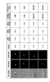
- FIG. 4 is a diagram illustrating an example of two two-dimensional images obtained by photographing a surface defect, a scale, and a harmless pattern, and a difference image thereof.
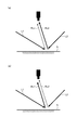
- FIG. 5 is a schematic diagram showing a configuration of an apparatus used in an experiment for investigating the relationship between the incident angle of illumination light and the reflectance of a healthy part (ground iron part).
- FIG. 1 is a schematic diagram showing a configuration of a surface defect detection apparatus according to a first embodiment of the present invention.
- FIG. 2 is a schematic diagram showing a configuration of a modification of the area sensor shown in FIG.
- FIG. 3 is a timing chart showing drive timings of the light source and the area sensor shown
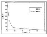
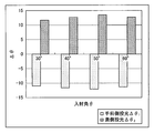
- FIG. 6 is a diagram showing the relationship between the incident angle of the laser and the amount of light received by the power meter.
- FIG. 7 is a schematic diagram for explaining the surface defect detection process according to the second embodiment of the present invention.
- FIG. 8 is a schematic diagram for explaining a surface defect detection process according to the third embodiment of the present invention.
- FIG. 9 is a schematic diagram illustrating the configuration of the apparatus used in the example.
- FIG. 10 is a diagram illustrating the surface defect detection processing result of the example.
- FIG. 11 is a diagram illustrating a surface defect detection processing result for a steel pipe portion where a scale has occurred.
- FIG. 12 is a schematic diagram showing a configuration of a modification of the surface defect detection device according to the first embodiment of the present invention.
- FIG. 13 is a schematic diagram showing the configuration of another modification of the surface defect detection device according to the first embodiment of the present invention.
- FIG. 14 is a diagram showing a shadow when illumination light is irradiated from one side when the surface shape of the examination target part is a concave shape or a convex shape.
- FIG. 15 is a diagram illustrating an example of a difference image of concave surface defects.
- FIG. 16 is a flowchart showing a flow of a method for calculating the positional relationship between the bright part and the dark part using the expansion process.
- FIG. 17 is a diagram illustrating an example of the one-dimensional profile of the difference image and the light / dark pattern.
- FIG. 18 is a diagram illustrating an example of a two-dimensional image and a one-dimensional profile of a filter.
- FIG. 19 is a diagram illustrating an example of a difference image and a one-dimensional profile that have been subjected to filter processing using the filter illustrated in FIG.
- FIG. 20 is a schematic diagram illustrating a modification of the arrangement position of the light sources.
- FIG. 21 is a schematic diagram showing a light / dark pattern obtained by the arrangement position of the light source shown in FIG.
- FIG. 22 is a diagram illustrating the surface defect detection processing result of the example.
- FIG. 23 is a diagram illustrating a difference image of the sagging habit.
- FIG. 24 is a diagram showing a differential image of the roll wrinkles when illumination light is irradiated from the width direction and the longitudinal direction of the thick steel plate.
- FIG. 25 is a diagram showing the inclination of surface defects when illumination light is irradiated from the width direction and the longitudinal direction of a thick steel plate.
- FIG. 26 is a diagram showing the inclination of the healthy part when illumination light is irradiated from the width direction of the thick steel plate.
- FIG. 27 is a diagram showing a configuration of a two-dimensional model of the optical system.
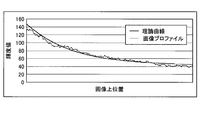
- FIG. 28 is a diagram illustrating a result of fitting an image profile to a theoretical curve.
- FIG. 29 is a diagram illustrating a configuration of an optical system.
- FIG. 30 is a diagram showing changes in signal intensity with respect to changes in the slope angle of surface defects when the incident angles of illumination light are 45 °, 60 °, and 75 °.
- FIG. 31 is a diagram showing a reflection model of illumination light on a healthy part surface and a highly diffusive surface.
- FIG. 32 is a diagram showing a difference image of the surface defect portion.
- FIG. 33 is a diagram showing an image obtained when illumination light is irradiated from the right and left directions on a thick steel plate on which a highly diffusible scale adheres to an uneven surface.
- FIG. 34 is a diagram illustrating a difference image between an image obtained when illumination light is irradiated from the right direction and an image obtained when illumination light is irradiated from the left direction.
- FIG. 35 is a diagram showing the configuration of the optical system.
- FIG. 36 is a diagram illustrating a change in the difference image with respect to a change in the incident angle of the illumination light.
- FIG. 37 is a diagram showing the standard deviation of the noise signal intensity at the position in the longitudinal direction before application of the moving average filter process.
- FIG. 38 is a diagram showing the standard deviation of the noise signal intensity at the position in the longitudinal direction after applying the moving average filter process.
- FIG. 39 is a diagram showing the relationship between the incident angle of illumination light and the difference in light transmission and reception between the near side and the far side.
- FIG. 40 is a diagram showing the relationship between the incident angle of illumination light and the absolute value of the difference between the light projecting / receiving difference on the near side and the light projecting / receiving difference on the far side.
- FIG. 41 is a diagram showing the configuration of the optical system.
- FIG. 42 is a diagram illustrating a detection result of surface defects.
- FIG. 43 is a diagram showing the detection result of barrage folds.
- FIG. 44 is a diagram showing the result of inspecting the surface defect while suppressing the visual field only in the longitudinal direction of the thick steel plate.
- FIG. 1 is a schematic diagram showing a configuration of a surface defect detection apparatus according to a first embodiment of the present invention.
- a surface defect detection device 1 according to a first embodiment of the present invention is a device that detects a surface defect of a cylindrical steel pipe P that is conveyed in the direction of an arrow in the figure, and includes light sources 2a and 2b.
- a function generator 3, area sensors 4a and 4b, an image processing device 5, and a monitor 6 are provided as main components.
- the light sources 2a and 2b irradiate the illumination light L that can be discriminated to the same inspection target portion on the surface of the steel pipe P in accordance with a trigger signal from the function generator 3. It is desirable that the light sources 2a and 2b be arranged symmetrically with respect to the inspection target part. Therefore, the light sources 2a and 2b are shifted by the same angle with respect to the normal vector of the surface of the steel pipe P, and are arranged so that the irradiation direction vector of the illumination light L and the normal vector of the surface of the steel pipe P are in the same plane. ing.
- the identity of the incident angle described here aims to make the optical conditions as equal as possible when discriminating light sources in different directions, and to greatly reduce the signal of a healthy part including a scale and a harmless pattern by differential processing. Further, the signal of the healthy part greatly depends on the surface property of the object, and it is difficult to guarantee the identity at a constant angle. Therefore, as long as the conditions can be inspected, even if the angles are slightly different, the same angle is expressed as long as the signal of the healthy portion can be reduced by the difference processing.
- the condition that can be inspected here is a condition that the specular reflection component can be sufficiently eliminated and the amount of light is sufficient. If the amount of light is sufficient, the incident angle may be made as large as possible.
- the number of light sources is two, but the number of light sources may be three or more as long as discrimination is possible.
- the discriminable light source described here refers to a light source capable of obtaining the amount of reflected light for each light source with respect to the reflected light obtained from the object.
- the area sensors 4a and 4b capture a two-dimensional image of the reflected light of the illumination light L emitted from the light sources 2a and 2b according to the trigger signal from the function generator 3.
- the area sensors 4 a and 4 b input captured two-dimensional image data to the image processing device 5. It is desirable that the area sensors 4a and 4b be installed on the normal vector of the region to be inspected as much as possible while ensuring the respective imaging fields of view.
- the area sensors 4a and 4b be as close as possible and the respective optical axes be as parallel as possible.
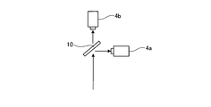
- the area sensors 4 a and 4 b may be adjusted so that the optical axes thereof are coaxial by using any one of the half mirror 10, the beam splitter, and the prism. Thereby, the difference image mentioned later can be acquired accurately.
- the image processing device 5 is a device that detects a surface defect in a region to be inspected by performing difference processing described later between two two-dimensional images input from the area sensors 4a and 4b.
- the image processing device 5 outputs to the monitor 6 information related to the two-dimensional images and surface defect detection results input from the area sensors 4a and 4b.
- the surface defect detection apparatus 1 having such a configuration discriminates the scale or harmless pattern from the surface defect in the inspection target part by executing the following surface defect detection process.
- the surface defects described here are irregular defects.
- the scale and harmless pattern mean a surface film with different optical characteristics and a surface property that is different from a steel part with a thickness of several ⁇ m to several tens of ⁇ m. It is a part to become.
- surface defect detection processing according to the first to third embodiments of the present invention will be described.
- FIG. 3 is a timing chart showing drive timings of the light sources 2a and 2b and the area sensors 4a and 4b.
- d represents the light emission time of the light sources 2a and 2b
- T represents the imaging period of the two-dimensional image by the area sensors 4a and 4b.
- the light sources 2a and 2b are discriminated by using the light sources 2a and 2b as flash light sources and repeatedly emitting light so that the flash light sources do not overlap each other.
- the function generator 3 transmits a trigger signal to the light source 2a and the area sensor 4a, the light source 2a emits the illumination light L, and the area sensor within time d. 4a completes the photographing of the two-dimensional image. Then, after the two-dimensional image is captured by the area sensor 4a, the function generator 3 transmits a trigger signal to the light source 2b and the area sensor 4b, and similarly captures the two-dimensional image. According to this embodiment, it is possible to take a two-dimensional image of each reflected light with respect to the illumination light L emitted from each light source without causing a decrease in the amount of light at the time difference d.
- the flash light source has a short light emission time d. This is because the shorter the light emission time d, the smaller the shutter delay between the two two-dimensional images obtained by the area sensors 4a and 4b, and the smaller the positional deviation of the two-dimensional image due to the shutter delay. Further, when it is intended to detect a surface defect using a difference image of a two-dimensional image by individual reflected light, the light emission time d of the flash light source needs to satisfy the condition shown in the following formula (2). .
- the conveyance speed of the steel pipe P is 1, 3, 5 m / sec.
- the light emission times of the light sources 2a and 2b must be 800, 270 and 160 ⁇ sec or less, respectively.
- this positional deviation can be corrected after photographing a two-dimensional image.
- the image processing apparatus 5 performs image processing such as calibration, shading correction, and noise removal using camera parameters derived in advance for the two-dimensional images input from the area sensors 4a and 4b. After the application, a surface defect in the inspection target part is detected by performing a difference process between the two-dimensional images.
- the luminance value of each pixel constituting the two-dimensional image Ia obtained when the illumination light L is emitted from the light source 2a is Ia (x, y) (where the number of pixels is X ⁇ Y, and the x coordinate is 1 ⁇ x ⁇ X, y coordinate is 1 ⁇ y ⁇ Y), and the luminance value of each pixel constituting the two-dimensional image Ib obtained when the illumination light L is irradiated from the light source 2b is expressed as Ib (x, y).
- the luminance value I_diff (x, y) of each pixel of the difference image I_diff is expressed by the following formula (3).
- FIGS. 4A, 4B, and 4C show examples of the two-dimensional images Ia and Ib and the difference image I_diff obtained by imaging the surface defect, the non-defect scale, and the harmless pattern, respectively.
- the luminance value I′_diff (x, y) of the difference image is expressed by the following formula (4).
- the light sources 2a and 2b are the same, and that each light source is irradiated so as to be as uniform parallel light as possible, and the inspection target part is close to a plane.
- surface defects can be detected by general shading correction even when the surface is somewhat uneven or when applied to a gently curved surface such as a steel pipe P.
- the incident angle of the illumination light L is within a range in which a specular reflection component does not enter the reflected light of the healthy part and a sufficient amount of light can be secured.
- the inventors of the present invention conducted an experiment for investigating the relationship between the incident angle of the illumination light L and the reflectance of the healthy part (ground iron part).
- the configuration of the apparatus used for the experiment is shown in FIG.
- the power meter 12 is fixed at a position on the normal vector l with respect to the target position on the surface of the slab sample 14.
- the amount of light received by the power meter 12 when the incident angle ⁇ of the laser 13 with respect to the normal vector l was changed from 0 ° to 90 ° was measured.
- the experimental results are shown in FIG.
- the incident angle ⁇ is in the range of 0 ° to 20 °
- the amount of light received by the power meter 12 is large because the specular reflection component is included, but when the incident angle ⁇ is 60 ° or more.
- the amount of light received by the power meter 12 is greatly reduced. Therefore, if the incident angle of the illumination light L is small as long as there is no problem in detection ability, the amount of received light can be increased.
- the resolution in the depth direction of the inspection target part depends on the inclination angle of the defect and the resolution of the area sensors 4a and 4b.
- the inclination angle of the defect means that the “normal vector of the defect part” is orthogonally projected onto the “plane formed by the normal vector of the surface of the healthy part of the inspection target site and the light source direction vector”, and the orthogonally projected vector And the normal vector of the surface of the healthy part.
- the light sources 2a and 2b are discriminated by using the light sources 2a and 2b as light sources whose wavelength regions do not overlap each other.
- the light sources 2a and 2b are discriminated by using the light sources 2a and 2b as light sources whose wavelength regions do not overlap each other.
- two types of wavelength selection filters 20a and 20b whose wavelength regions do not overlap with the light sources 2a and 2b are installed, and the wavelength region of the illumination light L is selected.
- wavelength selection filters 21a and 21b having the same wavelength selection characteristics are installed in the area sensors 4a and 4b.
- the reflected light of the illumination light L from the light source 2a is received only by the area sensor 4a by the wavelength selection filters 20a and 21a, and the reflected light of the illumination light L from the light source 2b is received by the wavelength selection filter 20b, Light is received only by the area sensor 4b by 21b. Therefore, by matching the photographing timings of the area sensors 4a and 4b, it is possible to photograph a two-dimensional image by the reflected light of the illumination light L from the light sources 2a and 2b without misalignment. Processing after taking a two-dimensional image is the same as in the first embodiment.
- the light sources 2a and 2b are used as flash light sources in order to prevent displacement due to the movement of the examination target part, and the two-dimensional operation is performed without changing the irradiation timing of the light sources 2a and 2b. You may shorten the imaging time of an image.
- the wavelength selection filter 20a is a blue transmission filter and the wavelength selection filter 20b is a green transmission filter
- a two-dimensional image is taken using a single color camera, so that the illumination light L from the light source 2a is captured in the blue channel. Only the reflected light may be received, and only the reflected light of the illumination light L from the light source 2b may be received by the green channel.
- the light sources 2a and 2b are discriminated by using the light sources 2a and 2b as light sources having linear polarization characteristics orthogonal to each other.
- linearly polarizing plates 30a and 30b are installed in the light sources 2a and 2b at ⁇ ° and ( ⁇ + 90) ° ( ⁇ is an arbitrary angle), and light components of polarization components orthogonal to each other.
- the linear polarizing plate means a filter that transmits only a linearly polarized light component in a certain direction with respect to incident light.
- linear polarizing plates 31a and 31b having the same linear polarization characteristics as the linear polarizing plates 30a and 30b are installed in the area sensors 4a and 4b at ⁇ ° and ( ⁇ + 90) °.
- the reflected light of the illumination light L from the light source 2a is received only by the area sensor 4a, and the reflected light of the illumination light L from the light source 2b is received only by the area sensor 4b. Therefore, by matching the photographing timings of the area sensors 4a and 4b, it is possible to photograph a two-dimensional image by the reflected light of the illumination light from each light source without misalignment.
- the light sources 2a and 2b may be flash light sources, and the imaging time of the two-dimensional image may be shortened without changing the irradiation timing of the light sources 2a and 2b.
- the processing after alignment and two-dimensional image capturing is the same as in the first and second embodiments.
- FIG. 9 shows a flash light source is used as the light sources 2a and 2b, and a surface defect of the steel pipe P is detected by using a method of changing the light emission timing of the light sources 2a and 2b.
- the area sensors 4a and 4b were juxtaposed to take a two-dimensional image and aligned by image processing.
- FIG. 10 shows the result of surface defect detection processing. 10A is a two-dimensional image obtained when the illumination light L is irradiated from the light source 2a, FIG. 10B is a two-dimensional image obtained when the illumination light L is irradiated from the light source 2b, and FIG. ) Is a difference image between the two-dimensional image shown in FIG.
- the SN ratios of the images shown in FIGS. 10A to 10C are 3.5, 3.5, and 6.0 in order, and the SN ratio of the difference image is higher than that when the illumination light L is simply emitted from one direction. Improved.
- FIG. 11 is a diagram showing the surface defect detection processing result for the steel pipe portion where the scale is generated.
- FIG. 11A shows a two-dimensional image obtained when the illumination light L is emitted from the light source 2a
- FIG. 11B shows a two-dimensional image obtained when the illumination light L is emitted from the light source 2b
- FIG. ) Is a difference image between the two-dimensional image shown in FIG. 11A and the two-dimensional image shown in FIG.
- a black spot spreading over the entire two-dimensional image shown in FIGS. 11A and 11B is a scale that causes noise. Since the scale shape was flat, the scale image was removed by acquiring the difference image. Moreover, in the difference image, the signal of the scale that becomes noise is reduced to about 1 ⁇ 4 as compared with the case where the illumination light L is simply irradiated from one direction.
- FIG. 12 is a schematic diagram showing a configuration of a modification of the surface defect detection device according to the first embodiment of the present invention.
- the illumination light irradiated from one light source 2a is divided by a plurality of mirrors 40a, 40b, 40c, and 40d, and finally the inspection target site of the steel pipe P1 is illuminated from two directions. Irradiate light.
- the same effects as those of the second and third embodiments can be obtained by installing the wavelength selection filters 20a and 20b and the linear polarizing plates 30a and 30b in the optical paths of the illumination light.
- this modification irradiates illumination light from two directions, it is the same when irradiating illumination light from three or more directions.
- FIG. 13 is a schematic diagram showing the configuration of another modification of the surface defect detection device according to the first embodiment of the present invention.
- the wavelength of the light source is not limited by the wavelength selection filters 20a and 20b, but the pulse lasers 51a and 51b and the diffusion plates 50a and 50b are used. Are used to limit the wavelength of the light source.
- the light sources are discriminated by irradiating laser light from two pulse lasers 51a and 51b having different wavelength regions from the left and right directions of the inspection target part.
- the diffusion plates 50a and 50b are inserted into the optical path of the laser light.
- this modification irradiates illumination light from two directions, it is the same when irradiating illumination light from three or more directions.
- This modification uses a dichroic mirror in place of the wavelength selection filters 21a and 21b installed in the area sensors 4a and 4b in the surface defect detection apparatus shown in FIG.
- a dichroic mirror is a mirror that reflects light of a specific wavelength component and transmits light of other wavelength components. By using a dichroic mirror, a wavelength selection filter becomes unnecessary.
- this modification irradiates illumination light from two directions, it is the same when irradiating illumination light from three or more directions.
- the surface defect detection apparatus 1 discriminates a scale or harmless pattern from an uneven surface defect in an inspection target part by executing the following surface defect detection process.
- the scale and harmless pattern mean a surface film or surface property with a different optical characteristic from a part of steel with a thickness of several ⁇ m to several tens of ⁇ m. It is a part.
- the image processing device 5 uses camera parameters derived in advance for two two-dimensional images input from the area sensors 4a and 4b. After performing image processing such as calibration, shading correction, and noise removal, a difference image is generated by performing difference processing between the two-dimensional images, and uneven surface defects in the inspection target part are generated from the generated difference image Is detected.
- the luminance value of each pixel constituting the two-dimensional image Ia obtained when the illumination light L is emitted from the light source 2a is Ia (x, y) (where the number of pixels is X ⁇ Y, and the x coordinate is 1 ⁇ x ⁇ X, y coordinate is 1 ⁇ y ⁇ Y), and the luminance value of each pixel constituting the two-dimensional image Ib obtained when the illumination light L is irradiated from the light source 2b is expressed as Ib (x, y).
- the luminance value I_diff (x, y) of each pixel of the difference image I_diff obtained by the difference processing is expressed by the above-described equation (3).
- luminance value I_diff (x, y) 0.
- FIGS. 14A and 14B are diagrams showing shadows when illumination light is irradiated from one light source to the inspection target part when the surface shape of the inspection target part is a concave shape and a convex shape.
- FIG. 14A when the surface shape of the inspection target part is a concave shape, the near side of the light source becomes dark due to a decrease in the amount of irradiation light per unit area, and the back side of the light source approaches the regular reflection direction. become brighter.
- FIG. 14A when the surface shape of the inspection target part is a concave shape, the near side of the light source becomes dark due to a decrease in the amount of irradiation light per unit area, and the back side of the light source approaches the regular reflection direction. Become brighter.
- FIG. 14A when the surface shape of the inspection target part is a concave shape, the near side of the light source becomes dark due to a decrease in the amount of irradiation light per unit area, and the back side of the light
- the near side of the light source becomes closer to the regular reflection direction so that it becomes brighter, and the back side of the light source has a convex shape. It becomes a shadow and darkens.
- the light / dark pattern of the reflected light of the illumination light differs depending on whether the surface shape of the inspection target part is concave or convex. Therefore, the presence or absence of uneven surface defects can be detected by recognizing the light / dark pattern of the reflected light. Therefore, in the following, a method for detecting uneven surface defects by recognizing a light / dark pattern of reflected light will be described. In the following description, it is assumed that concave surface defects are detected among uneven surface defects, but convex surface defects can also be detected by the same logic.
- the bright part described below means a blob having an area of a predetermined value or more obtained by performing a concatenation process on a pixel whose luminance is a predetermined threshold or more in the difference image I_diff.
- the dark portion described below refers to a blob having an area greater than or equal to a predetermined value obtained by performing concatenation processing on pixels whose luminance is equal to or lower than a predetermined threshold in the difference image I_diff.
- a blob means a set of labeled pixels.
- a light / dark pattern is recognized by extracting a bright part and a dark part by performing threshold processing.
- the light sources 2a and 2b are arranged symmetrically with respect to the normal vector of the inspection target part, so that the reflected light caused by the uneven shape on the surface is reflected.
- Light and dark patterns occur in the left-right direction. Since the right and left of the light and dark are reversed depending on the order of the difference processing, here, the right is bright and the left is dark, the concave shape, the right is dark, and the left is bright is the convex shape. Therefore, the difference image I_diff of the concave surface defect is as shown in FIG. Therefore, if the bright part image and the dark part image are binarized by the luminance threshold values The and -The, respectively, the bright part and dark part binarized images I_blight and I_dark are respectively expressed by the following formula (5).
- the first positional relationship calculation method is a method of calculating the positional relationship between the bright part and the dark part by performing an expansion process in a specific direction on the bright part and the dark part.
- a flowchart of this calculation method is shown in FIG.
- a case will be described in which a bright and dark pattern in which the right is bright and the left is dark in order to detect a concave surface defect is recognized.
- Light on the right and dark on the left means that there is always a dark part on the left side of the bright part, and there is always a bright part on the right side of the dark part.
- the image processing apparatus 5 performs an expansion process in the right direction for the dark part and performs an expansion process in the left direction for the bright part (steps S1a and S1b).
- the expansion process is expressed as Equation (6) below.
- the upper left of the two-dimensional image is the origin
- the lower direction is positive in the y-axis direction
- the right direction is positive in the x-axis direction.
- the bright portion and the dark portion are expanded by the same length W, but the expanded length W is not necessarily the same. In extreme cases, only the bright portion and the dark portion are included. On the other hand, an expansion process may be performed. Further, the expanding length W depends on the size of the surface defect to be detected.
- the image processing apparatus 5 performs an expansion process by performing an AND process on the bright and dark images I_blight_extend and I_dark_extend that have been subjected to the expansion process as in Expression (7) below.
- the overlapping part of the bright part and dark part images I_blight_extend and I_dark_extend is extracted as a defect candidate part image I_defect (steps S2a and S2b).
- the image processing apparatus 5 generates a defect candidate blob I_defect_blob by performing a labeling process on the obtained defect candidate part images I_defect after performing a connection / isolated point removal process as necessary. (Step S3). Then, the image processing device 5 extracts the feature amount of each defect candidate blob I_defect_blob, and determines whether each defect candidate blob I_defect_blob is a concave surface defect based on the extraction result (steps S4a and S4b). . Note that in order to investigate the feature amount of the defect candidate blob I_defect_blob, information on the bright part and the dark part is necessary, so the bright part and the dark part are restored from the defect candidate blob I_defect_blob.
- the image processing apparatus 5 since the bright part always exists on the right side of the defect candidate part and the dark part always exists on the left side, the image processing apparatus 5 starts from the center of gravity of the defect candidate blob I_defect_blob as the starting point, and the dark part binarized image I_dark. To the left, and the first found blob is a dark defect candidate blob I_dark_blob. Similarly, the image processing apparatus 5 searches the right part binarized image I_blight on the right side starting from the center of gravity of the defect candidate blob I_defect_blob, and sets the first found blob as the bright part defect candidate blob I_blight_blob.
- the image processing apparatus 5 extracts the feature amount from the bright part defect candidate blob I_blight_blob and the dark part defect candidate blob I_dark_blob restored in this manner, and each defect candidate blob I_defect_blob is a concave surface defect based on the extracted feature quantity. It is determined whether or not. Since the specific feature amount varies depending on the defect, an example will be given in an embodiment described later without being described here.
- the second positional relationship calculation method after performing the above-described threshold processing and performing connection / isolated point removal processing as necessary, the bright portion and the dark portion are extracted and labeling is performed, and the positions of the bright portion and the dark portion are determined. Recognizing the relationship detects a concave surface defect. Specifically, first, the image processing apparatus 5 individually recognizes the bright part and the dark part by labeling, and obtains the gravity center information of the bright part and the dark part. Next, the image processing apparatus 5 determines whether the center of gravity of the dark part exists within a predetermined range on the right side of each bright part from the center of gravity information of the bright part and the dark part.
- the image processing apparatus 5 recognizes the combination of a bright part and a dark part which are a pair as a bright and dark pattern, and performs feature quantity analysis of the bright and dark pattern, thereby detecting a concave surface defect. It is determined whether or not there is.
- the light / dark pattern is recognized using the center-of-gravity information.
- the information used for recognizing the light / dark pattern is not necessarily the center of gravity information Not necessary.
- FIGS. 17A and 17B are diagrams showing an example of a difference image and a one-dimensional profile of a light-dark pattern in the line segment L4 shown in FIG.
- the concave surface defects are bright on the right and dark on the left. Therefore, the one-dimensional profile of the light / dark pattern is characteristic of a mountain shape on the right side and a valley shape on the left side. Become a one-dimensional profile. Therefore, in the present embodiment, a filter H having a mountain shape on the right side and a valley shape on the left side is created in advance, and the filter H is applied to the difference image I_diff as shown in the following formula (8), whereby a high frequency is obtained. A two-dimensional image I_cont in which noise is reduced and only a light / dark pattern is enhanced is generated.
- FIGS. 18 (a) and 18 (b) are diagrams showing an example of a two-dimensional image of the filter H created in advance and a one-dimensional profile thereof in the left-right direction.
- FIGS. 19A and 19B are diagrams showing an example of the difference image subjected to the filter processing using the filter H shown in FIGS. 18A and 18B and the one-dimensional profile thereof in the left-right direction. is there. As shown in FIGS. 19A and 19B, it can be seen that a two-dimensional image in which high-frequency noise is reduced and only the bright and dark pattern is enhanced is obtained.
- the image processing device 5 performs a threshold value process on the defect candidate portion image I_defect after performing a connection / isolation point removal process on the two-dimensional image with the bright / dark pattern enhanced in this way as necessary. Extract. Then, the image processing apparatus 5 detects a concave surface defect by performing the same processing as the first positional relationship calculation method on the extracted defect candidate portion image I_defect.
- the surface defect detection processing according to the second embodiment of the present invention is performed by using the two light sources 2a and 2b that can be discriminated from each other in substantially the same direction from different directions.
- Illumination light L is irradiated at an incident angle, images obtained by reflected light of each illumination light L are acquired, and a bright part and a dark part of an image obtained by performing a difference process between the acquired images are extracted and extracted. Since the presence or absence of uneven surface defects is determined from the positional relationship between the bright part and the dark part and the irradiation direction of the illumination light L, it is possible to accurately discriminate between scales and harmless patterns and uneven surface defects.
- the left and right light and dark patterns are recognized because the light sources are installed symmetrically.
- the same processing is performed.
- Defects can be detected. Specifically, when the light sources are arranged vertically symmetrically, the light / dark pattern only changes from the horizontal direction to the vertical direction. Defects can be detected.
- the surface defect when the light sources 2a and 2b are installed so that the illumination direction of illumination light is different by 90 °, if the surface defect is concave, the near side of the light source is dark and the back side is bright, and the surface defect If is convex, the front side of the light source is bright and the back side is dark.
- the surface defect has a concave shape
- the two-dimensional image obtained by the illumination light from the light source 2a is as shown in FIG. 21A
- the two-dimensional image obtained by the illumination light from the light source 2b Is as shown in FIG. For this reason, the difference image becomes a bright and dark pattern having contrast from the lower left to the upper right as shown in FIG.
- the uneven surface defect is detected when the illumination light is irradiated from the direction that is symmetric with respect to the normal line of the inspection target part, but the irradiation direction of the illumination light is not necessarily symmetric. Moreover, the surface defect detection process of this embodiment can be applied to the entire production line of steel regardless of whether it is hot or cold.
- the surface defect detection process using the first positional relationship calculation method is applied to the inspection target portion where the pit ridge is formed and the healthy inspection target portion where the pit ridge is not formed.
- the brightness ratio, area ratio, and circularity of the bright part and the dark part were calculated as the feature amount.
- the circularity is a value obtained by dividing the area of the bright part and the dark part by the square of the circumference of the circumference, and is used when determining whether the shape of the bright part and the dark part is close to a circular shape. .
- the surface defect has the same cause, it is unlikely that the luminance and area are significantly different between the left and right signals, and the detection accuracy of the surface defect is improved by evaluating the left and right balance using the luminance ratio and area ratio. Further, in order to evaluate the shadow, the bright part and the dark part rarely have a circular shape, and it is possible to determine that a thing close to the circular shape is caused by another, so the circularity is incorporated into the feature amount. In addition, the areas of the bright part and the dark part are calculated so that only surface defects whose area is a predetermined value or more can be detected. The detection result is shown in FIG. As shown in FIG. 22, according to the present Example, it was confirmed that the pit ridge and the healthy part in which the pit ridge was not formed can be distinguished with high accuracy.
- FIG. 23 is a diagram showing a result of detecting a surface defect called a drop defect using the surface defect detection method according to the present invention.
- the depression wrinkles can be detected firmly by the light and dark pattern.
- the intensity of the defect signal was increased as shown in FIG.
- the inventors of the present invention measure the shape of the surface defects, and determine the inclination of the surface defects when the illumination light is irradiated from the width direction of the thick steel plate and when the illumination light is irradiated from the longitudinal direction of the thick steel plate. Calculated.
- the inclination described here is obtained by orthogonally projecting the normal vector of each surface of the thick steel plate and the normal vector of the reference surface of the thick steel plate onto the plane formed by the light source, the area sensor, and the inspection target position, respectively. It means the angle formed by two vectors.
- FIG. 25 shows the calculation result. As shown in FIG.
- the inclination of the surface defect when irradiated with illumination light from the width direction of the thick steel plate was 7 ° or less, whereas as shown in FIG.
- the inclination of surface defects when irradiated with illumination light from the longitudinal direction of the steel sheet was about 20 ° to 30 °.
- the pattern which looks like a stripe when illuminating light is irradiated from the width direction of a thick steel plate is harmless scale peeling.
- the shape of the healthy part was measured in the same manner and the inclination of the healthy part when the illumination light was irradiated from the width direction of the thick steel plate, the inclination of the healthy part was 3 ° as shown in FIG.
- FIG. 27 is a diagram showing a configuration of a two-dimensional model of the optical system.
- the incident angle of the illumination light L from the light source 2 on the steel material surface S (normal vector l) to the target position is ⁇
- the reflection angle of the illumination light L incident on the area sensor 4 is ⁇
- the steel material The inclination of the reference surface of the surface S is assumed to be 0, the inclination when the inspection target part is captured microscopically, the incident light amount of the illumination light L from the light source 2 to the inspection target part is I 0 , and the surface property of the inspection target part is expressed.
- the light quantity i of the illumination light L incident on the area sensor 4 is expressed by the following formula (9).
- R in the formula (9) represents a function of the reflection intensity of the illumination light L, and is calculated by the following formula (10).
- the first term on the right side of Equation (10) represents the intensity of diffuse reflection of the illumination light L
- the second term represents the intensity of specular reflection of the illumination light L
- the reflection intensity of the illumination light L is the first term. It is expressed as the sum of the second term.
- diffuse reflection the illumination light L is diffused in all directions after being incident on the inspection target site.
- specular reflection the illumination light L is reflected most strongly in a direction symmetric with respect to the normal vector of the region to be inspected, and the intensity of the illumination light L attenuates in a Gaussian function as the distance from the direction increases.
- k (K 1 , K 2 , ⁇ ) is a term resulting from the surface properties of the examination target site, and determines the extent of specular reflection and the intensity ratio of specular reflection and diffuse reflection.
- the incident angle ⁇ and the inclination ⁇ satisfy the condition: ⁇ / 2 ⁇ ⁇ + ⁇ or ⁇ + ⁇ ⁇ ⁇ / 2, the portion to be inspected itself becomes a shadow and the illumination light L is not irradiated.
- the reflection intensity of the illumination light L is zero.
- the intensity of the image signal received by the area sensor 4 is expressed using such a two-dimensional model, illumination light is emitted from one (left side) light source and illumination light is emitted from the other (right side) light source.
- the luminances i 1 and i 2 of a certain point (hereinafter referred to as a target surface) on the image of the inspection target region are calculated, the luminances i 1 and i 2 are expressed by the following formulas (11) and (12).
- I 1 and I 2 are the amounts of light incident on the target surface of the illumination light L
- ⁇ 1 and ⁇ 2 are the incidence of illumination light from each light source on the target position of the target surface.
- Angle ⁇ is a reflection angle of the illumination light L incident on the area sensor 4
- ⁇ is a tilt when the target surface is captured microscopically with the tilt of the reference surface of the target surface being zero
- k is a parameter representing the surface property of the target surface. It is.
- shading correction is performed on the luminances i 1 and i 2 in order to remove unevenness in the light amount of the light source 2 and unevenness in optical conditions.
- a row vector (called “vertical average vector”), which is generally used here, is an average obtained by adding the luminance of each pixel in the vertical direction. It was created by subtracting and dividing the vertical average vector for all rows of the image, and further normalizing the signal by a constant multiplication. The resulting image was further subjected to the same processing in the horizontal direction for shading correction.
- the target surface is a healthy part
- the signal is represented by i 10 and i 20
- the surface property of the healthy part is represented by k 0, which is expressed by the following formulas (13) and (14). .
- Equation (15) represents the luminance i 1 after shading correction
- Equation (16) represents the luminance i 2 after shading correction
- Equation (17) represents the luminance on the difference image.
- the optimal range of the incident angle of illumination light was derived from the intensity of the image signal of the healthy part and the surface defect part using the above model.
- parameters representing the surface properties of the steel surface were experimentally determined. Specifically, an actual image of the brightness profile (theoretical curve) of a theoretical image signal obtained by simulating the same optical system by taking an image of a steel material having general surface properties with an area sensor. The luminance profile (image profile) of the image signal was adjusted.
- FIG. 28 shows the result of fitting
- FIG. 29 shows the configuration of the optical system used in the experiment.
- FIG. 30 is a diagram illustrating a change in signal intensity with respect to a change in the slope angle of the surface defect when the incident angle ⁇ to the defect position of the illumination light is 45 °, 60 °, and 75 °.
- the signal strength increases as the slope angle of the surface defect increases. That is, when the illumination light is irradiated from the width direction of the thick steel plate, that is, the width direction with respect to the roll wrinkles, the signal strength is not greatly different from the surface property because the inclination of the surface defect portion is the same inclination as the surface property.
- the illumination light is irradiated from the longitudinal direction of the thick steel plate, since the inclination of the surface defect portion is larger than the inclination of the healthy portion, the signal intensity is increased and the surface defect is detected. Can do.
- this example is an example of the surface defect long in the width direction of a thick steel plate
- the surface defect long in the longitudinal direction of a thick steel plate exists similarly. Therefore, in order to suppress oversight of surface defects and detect all surface defects, it is necessary to irradiate illumination light from two directions of the thick steel plate in the width direction and the longitudinal direction.
- an oversight occurs. For this reason, also in this case, it is necessary to irradiate illumination light from the two directions of the width direction and the longitudinal direction of the thick steel plate.
- the present invention is characterized in that a difference image is obtained by irradiating an examination target site from two or more different directions, but in the following, for the sake of simplification, they are symmetrical with respect to the normal vector of the steel surface.
- illumination light is emitted when illumination light is irradiated from one light source (for convenience, irradiation from the right direction) and when illumination light is irradiated from the other light source (for convenience, irradiation from the left direction).
- the conditions regarding the incidence and reflection of the light are preferably the same.
- FIG. 31A shows a reflection model of illumination light on the surface of the healthy part
- FIG. 31B shows a reflection model of illumination light on the surface with high diffusivity.
- the thickness of the line represents the amount of illumination light.
- the specular reflection condition described above is a condition in which the light source and the area sensor are located symmetrically with respect to the normal vector of the healthy part surface, that is, a condition where the incident angle and the reflection angle of the illumination light are equal. is there.
- the image signal value of the surface defect portion is the same as the sound portion. Higher than the surface portion.
- Such changes in specularity and diffusivity due to the surface texture do not occur in the optical system where the light source is symmetrical with respect to the optical axis of the area sensor, that is, in the center of the field of view, so the balance between the left and right projection and reception angles of the illumination light
- the collapse of the noise is considered to be the noise factor of this method.
- An example of the difference image obtained from the thick steel plate is shown in FIG. In the example shown in FIG. 32, the appearance of surface defects differs depending on the position of the visual field.
- the left side of the visual field (FIG. 32A) is generally brighter and the right side (FIG. 32C) is generally darker.
- the diffusibility of the surface defect portion is high, the signal intensity is higher than the healthy portion when the distance from the specular reflection condition is increased.
- the bright and dark pattern can be confirmed firmly at the center of the field of view (FIG. 32B), but at the edge of the field of view, an offset occurs in the image luminance due to the diffusivity, and only the bright part or dark part is present. Therefore, in the present invention, since the surface defect is detected using the bright and dark pattern, it is difficult to detect the surface defect at the field edge.
- FIGS. 33 (a) and 33 (b) show images obtained when illumination light is irradiated from the right and left directions, respectively, on a thick steel plate having a highly diffusible scale attached to an uneven surface.
- FIG. FIG. 34 is a diagram illustrating a difference image between an image obtained when illumination light is irradiated from the right direction and an image obtained when illumination light is irradiated from the left direction.
- the left side of the screen when illuminated from the left side is “front side”
- the right side of the screen is “back side”
- the left side of the screen when illuminated from the right direction is “back side”
- the right side of the screen is “front side” "Side”.
- the method for evaluating the difference image is described below.
- shading correction is performed in order to remove unevenness in the amount of light in each difference image.
- the luminance of each pixel is added in the vertical direction to obtain an average.
- a row vector (referred to as a “vertical average vector”) was created, and all the rows of the image were subtracted and divided by the vertical average vector, and the signal was multiplied by a constant and normalized.
- the resulting image was further subjected to the same processing in the horizontal direction for shading correction.
- FIG. 36 shows the result of taking the difference image of the image subjected to the shading correction in this way.
- the test was carried out with two samples having the same surface texture arranged side by side in order to secure the field of view, so that a joint is generated in the center, but this portion is excluded and the peripheral pixels are excluded. I'm filling in the hole.
- FIG. 36 it was confirmed that the range without the noise signal was increased as the incident angle ⁇ of the illumination light was increased.
- the incident angle ⁇ is 70 ° or 80 °, the signal due to the fine irregularities on the surface is emphasized and becomes a noise factor, which is difficult to distinguish from the noise due to the surface property. Exclude from further consideration.
- the standard deviation of the noise signal intensity in the longitudinal direction was calculated.
- the calculation results are shown in FIG.
- the standard deviation of the noise signal intensity increases as it approaches the longitudinal end.
- the moving average filter process is performed on the waveform shown in FIG. 37 to smooth the waveform.
- the standard deviation of the noise signal intensity is the smallest at the center part and is about 2, and the standard deviation of the noise signal intensity increases toward the end part. Since the signal strength of the surface defect to be detected is about 15, the standard deviation of the noise signal strength must be 5 or less in order to ensure an SN ratio of 3 or more, which is generally said to be detectable.
- the light transmission / reception difference ⁇ described here is expressed by the following formula (18) using the incident angle ⁇ and the reflection angle ⁇ of the illumination light to the defect position in the inspection target site, and the light projection / reception angle of the illumination light is the sample. It is a value indicating how close or far the specular reflection direction is compared with the case where the center Sc is irradiated. The sign is positive in the direction away from regular reflection.
- the calculation results are shown in FIGS. FIG.
- FIG. 39 is a diagram illustrating a change in the light transmission / reception difference ⁇ on the near side and the far side with respect to the change in the incident angle of the illumination light at the end of the range where the standard deviation of the noise signal intensity is 5 or less.
- FIG. 40 shows the difference between the light transmission / reception difference ⁇ 1 on the near side and the light transmission / reception difference ⁇ 2 on the back side with respect to the change in the incident angle of the illumination light at the end of the range where the standard deviation of the noise signal intensity is 5 or less. It is a figure which shows the change of an absolute value.
- the light transmission / reception differences ⁇ 1 and ⁇ 2 on the near side and the back side change according to the incident angle of the illumination light. Yes.
- the light transmission / reception difference ⁇ 1 on the near side and the light transmission / reception difference ⁇ on the back side the absolute value of the difference between the 2
- the surface defect detection processing according to the present invention is executed so that the irradiation angle and the light receiving angle satisfy the above conditions from the optical system at the center of the sample, noise caused by the surface properties can be suppressed to some extent.
- a 1 indicates a regular reflection direction of the illumination light incident on the examination target site from one of the two light sources, and a direction of the area sensor 4 of the illumination light entered from one light source in the examination target site.
- a 2 a vector indicating the specular reflection direction of the illumination light from the other light source incident on the inspected portion of the vector indicating a reflection direction b 1, 2 one light source to, incident from the other light source in the inspected portion
- the vectors a 1 , b 1 , a 2 , and b 2 may satisfy the following formula (1). That is, ⁇ 1 is expressed using vectors a 1 and b 1 , and ⁇ 2 is expressed using vectors a 2 and b 2 .
- the steel material is a thick steel plate, but the present invention can be similarly applied to a thin steel plate.
- the number of area sensors and light sources becomes enormous because the plate width of the thick steel plate is wide. Requires a lot of cost.
- two cases are considered, where illumination light is irradiated from the width direction of the thick steel plate and illumination light is irradiated from the longitudinal direction of the thick steel plate.
- the condition shown in the above formula (18) if an optical system is designed so as to satisfy the condition in the width direction of the thick steel plate, the field of view in the width direction per area sensor is limited.
- the visual field in the longitudinal direction per area sensor can be arbitrarily designed by designing the capture cycle in accordance with the moving speed of the thick steel plate. Therefore, when the illumination light is irradiated from the longitudinal direction of the thick steel plate among the two directions of the width direction and the longitudinal direction of the thick steel plate, in other words, one illumination light of the illumination light irradiated by the two light sources. Only when the irradiation direction is parallel to the longitudinal direction of the steel material, the optical system is designed so as to satisfy the condition shown in Formula (1), and when the illumination light is irradiated from the width direction of the thick steel plate, it is used as an auxiliary. It is desirable to do. Thereby, it can test
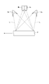
- FIG. 41 is a schematic diagram showing the configuration of the optical system used in the experiment.
- the same components as those in FIG. 35 are denoted by the same reference numerals.
- the positional relationship among the area sensor 4, the two light sources 2, the sample (thick steel plate) S, and the sample center Sc is the same as that in FIG.
- the incident angle ⁇ of illumination light is 70 °
- the resolution of the area sensor is 1.0 mm / pixel
- the inspection range is 350 mm ⁇ 270 mm.
- FIG. 42 shows the result of detection of surface defects. As shown in FIG.
- the detection result of the surface defect represents a portion where the bright part and the dark part are expanded and overlapped, and the threshold value of the signal intensity is 15.
- FIG. 43 is a diagram showing the detection result of a surface defect that is long in the longitudinal direction, which is called a barrio ridge.
- a surface defect that is long in the longitudinal direction, which is called a barrio ridge.
- FIG. 43 (c) when the illumination light is irradiated from the longitudinal direction of the thick steel plate, the signal intensity is very low, but as shown in FIG. 43 (b), the illumination light is applied from the width direction of the thick steel plate. When irradiated, the light / dark pattern was confirmed.
- FIG. 44 is a figure which shows the result of having investigated the surface defect, suppressing a visual field only in the longitudinal direction of a thick steel plate.
- the inspection target was a steel plate with poor surface properties.
- FIG. 44 it was confirmed that the position where the projection / reception angle balance of the illumination light is bad becomes a noise factor, and that the inspection can be performed under the condition where the balance of the projection / reception angle is good by limiting the inspection range.
- a surface defect of a steel material may be detected using the surface defect detection method according to the present invention, and the steel material may be manufactured based on the detection result.
- other embodiments, examples, operation techniques, and the like made by those skilled in the art based on the present embodiment are all included in the scope of the present invention.
- the present invention it is possible to provide a surface defect detection device and a surface defect detection method capable of accurately discriminating between scales and harmless patterns and surface defects. Moreover, according to this invention, the manufacturing method of the steel materials which can discriminate a scale, a harmless pattern, and a surface defect accurately, and can manufacture steel materials based on a discrimination result can be provided.
Landscapes
- Physics & Mathematics (AREA)
- Health & Medical Sciences (AREA)
- Life Sciences & Earth Sciences (AREA)
- Chemical & Material Sciences (AREA)
- Analytical Chemistry (AREA)
- Biochemistry (AREA)
- General Health & Medical Sciences (AREA)
- General Physics & Mathematics (AREA)
- Immunology (AREA)
- Pathology (AREA)
- Engineering & Computer Science (AREA)
- Textile Engineering (AREA)
- Investigating Materials By The Use Of Optical Means Adapted For Particular Applications (AREA)
Abstract
Description


初めに、図1から図13を参照して、本発明の第1の実施形態である表面欠陥検出装置の構成及びその動作について説明する。
図1は、本発明の第1の実施形態である表面欠陥検出装置の構成を示す模式図である。図1に示すように、本発明の第1の実施形態である表面欠陥検出装置1は、図示矢印方向に搬送される円筒形状の鋼管Pの表面欠陥を検出する装置であり、光源2a,2b、ファンクションジェネレータ3、エリアセンサ4a,4b、画像処理装置5、及びモニター6を主な構成要素として備えている。
初めに、図3から図6を参照して、本発明の第1の実施態様である表面欠陥検出処理について説明する。



次に、図7を参照して、本発明の第2の実施態様である表面欠陥検出処理について説明する。
次に、図8を参照して、本発明の第3の実施態様である表面欠陥検出処理について説明する。
本実施例では、図9に示すように、光源2a,2bとしてフラッシュ光源を用い、光源2a,2bの発光タイミングを変化させる方法を用いて鋼管Pの表面欠陥を検出した。エリアセンサ4a,4bは並列させて2次元画像を撮影し、画像処理により位置合わせを行った。図10に表面欠陥の検出処理結果を示す。図10(a)が光源2aから照明光Lを照射した時に得られた2次元画像、図10(b)が光源2bから照明光Lを照射した時に得られた2次元画像、図10(c)が図10(a)に示す2次元画像と図10(b)に示す2次元画像との差分画像である。図10(a)~(c)に示す画像のSN比は順に3.5、3.5、6.0であり、単に一方向から照明光Lを照射した場合よりも差分画像のSN比が向上した。
図12は、本発明の第1の実施形態である表面欠陥検出装置の変形例の構成を示す模式図である。図12に示すように、本変形例は、1つの光源2aから照射した照明光を複数のミラー40a,40b,40c,40dにより分割し、最終的に2方向から鋼管P1の検査対象部位に照明光を照射する。この場合、照明光の各光路に波長選択フィルター20a,20bや直線偏光板30a,30bを設置することにより、第2及び第3の実施態様と同様の効果を得ることができる。なお、本変形例は照明光を2方向から照射するものであるが、3方向以上から照明光を照射する場合も同様である。
図13は、本発明の第1の実施形態である表面欠陥検出装置の他の変形例の構成を示す模式図である。図13に示すように、本変形例は、図7に示す表面欠陥検出装置において、波長選択フィルター20a,20bによって光源の波長を限定するのではなく、パルスレーザー51a,51bと拡散板50a,50bとを用いて光源の波長を限定するものである。本変形例では、互いに波長領域が異なる2つのパルスレーザー51a,51bからのレーザー光を検査対象部位の左右方向から照射して光源を弁別する。このとき、パルスレーザー51a,51bから照射されたレーザー光を検査対象部位全域に照射するためにレーザー光の光路に拡散板50a,50bを挿入する。なお、本変形例は2方向から照明光を照射するものであるが、3方向以上から照明光を照射する場合も同様である。
本変形例は、図7に示す表面欠陥検出装置において、エリアセンサ4a,4bに設置する波長選択フィルター21a,21bの代わりにダイクロイックミラーを用いるものである。ダイクロイックミラーとは、特定の波長成分の光を反射し、その他の波長成分の光を透過するミラーのことである。ダイクロイックミラーを用いることによって波長選択フィルターが不要となる。なお、本変形例は2方向から照明光を照射するものであるが、3方向以上から照明光を照射する場合も同様である。
次に、図14から図22を参照して、本発明の第2の実施形態である表面欠陥検出装置の構成及びその動作について説明する。なお、本実施形態の表面欠陥検出装置の構成は上記第1の実施形態の表面欠陥検出装置の構成と同じであるので、以下ではその構成の説明を省略し、表面欠陥検出装置の動作についてのみ説明する。
本発明の第2の実施形態である表面欠陥検出処理では、画像処理装置5が、エリアセンサ4a,4bから入力された2つの2次元画像に対して予め導出しておいたカメラパラメータを用いてキャリブレーション、シェーディング補正、及びノイズ除去等の画像処理を施した後、2次元画像間で差分処理を行うことによって差分画像を生成し、生成された差分画像から検査対象部位における凹凸性の表面欠陥を検出する。


本実施例では、ピット疵が形成されている検査対象部位とピット疵が形成されていない健全な検査対象部位に対して上記第1の位置関係算出方法を用いた表面欠陥検出処理を適用した。本実施例では、特徴量として、明部及び暗部の輝度比、面積比、及び円形度を算出した。円形度とは、明部及び暗部の面積をその周の長さの二乗で割って正規化した値であり、明部及び暗部の形状が円形状に近いか否かを判定する際に用いられる。同一起因の表面欠陥であれば、左右の信号で輝度や面積が著しく異なるということは考えにくく、輝度比や面積比を用いて左右のバランスを評価することによって表面欠陥の検出精度が向上する。また、陰影を評価するため明部及び暗部が円形状になることはほとんどなく、円形状に近いものは別起因であると判断できるために、特徴量に円形度を組み入れた。また、明部及び暗部の面積を算出し、面積が所定値以上である表面欠陥のみを検出できるようにした。検出結果を図22に示す。図22に示すように、本実施例によれば、ピット疵とピット疵が形成されていない健全部とを精度よく弁別できることが確認された。
次に、本発明に係る表面欠陥検出方法を用いて厚鋼板の表面欠陥を検出する場合における照明光の入射角及び表面欠陥の検出能について検討する。図23は、本発明に係る表面欠陥検出方法を用いて落ち込み疵と呼ばれる表面欠陥を検出した結果を示す図である。図23に示すように、明暗パターンによって落ち込み疵をしっかりと検出できていることがわかる。しかしながら、ロール疵と呼ばれる表面欠陥については、厚鋼板の幅方向に照明光を照射した時は、図24(a)に示すように、ロール疵の形状が細長いために欠陥信号をほとんど確認することができないが、厚鋼板の長手方向に照明光を照射した時には、図24(b)に示すように、欠陥信号の強度が強まることが確認された。







最後に、表面欠陥の検査範囲及びノイズ要因について検討する。本発明は、2つ以上の異なる方向から検査対象部位に照明光を照射して差分画像を取得することを特徴としているが、以下では簡易化のため鋼材表面の法線ベクトルに関して互いに対称な斜め方向から照明光を照射する場合を例として、光学系の条件について検討する。この場合、一方の光源から照明光を照射した時(便宜上、右方向からの照射とする)と他方の光源から照明光を照射した時(便宜上、左方向からの照射とする)とで照明光の入射及び反射に関する条件は同じであることが好ましい。

2a,2b 光源
3 ファンクションジェネレータ
4a,4b エリアセンサ
5 画像処理装置
6 モニター
L 照明光
P 鋼管
Claims (7)
- 鋼材の表面欠陥を光学的に検出する表面欠陥検出装置であって、
2つ以上の弁別可能な光源を利用して同一の検査対象部位に異なる方向から照明光を照射する照射手段と、
各照明光の反射光による画像を取得し、取得した画像間で差分処理を行うことによって前記検査対象部位における表面欠陥を検出する検出手段と、を備え、
2つの光源のうちの一方の光源から前記検査対象部位に入射した照明光の正反射方向を示すベクトルをa1、前記検査対象部位における前記一方の光源から入射された照明光の前記画像を撮影する撮影手段方向への反射方向を示すベクトルをb1、2つの光源のうちの他方の光源から前記検査対象部位に入射した照明光の正反射方向を示すベクトルをa2、前記検査対象部位における前記他方の光源から入射された照明光の前記画像を撮影する撮影手段方向への反射方向を示すベクトルをb2とした時、前記検査対象部位においてベクトルa1、ベクトルb1、ベクトルa2、及びベクトルb2が以下に示す数式(1)を満足することを特徴とする表面欠陥検出装置。

- 2つの光源によって照射される照明光のうちの一つの照明光の照射方向が鋼材の長手方向に平行であることを特徴とする請求項1に記載の表面欠陥検出装置。
- 鋼材の表面欠陥を光学的に検出する表面欠陥検出方法であって、
2つ以上の弁別可能な光源を利用して同一の検査対象部位に異なる方向から照明光を照射する照射ステップと、
各照明光の反射光による画像を取得し、取得した画像間で差分処理を行うことによって前記検査対象部位における表面欠陥を検出する検出ステップと、を含み、
2つの光源のうちの一方の光源から前記検査対象部位に入射した照明光の正反射方向を示すベクトルをa1、前記検査対象部位における前記一方の光源から入射された照明光の前記画像を撮影する撮影手段方向への反射方向を示すベクトルをb1、2つの光源のうちの他方の光源から前記検査対象部位に入射した照明光の正反射方向を示すベクトルをa2、前記検査対象部位における前記他方の光源から入射された照明光の前記画像を撮影する撮影手段方向への反射方向を示すベクトルをb2とした時、前記検査対象部位においてベクトルa1、ベクトルb1、ベクトルa2、及びベクトルb2が以下に示す数式(1)を満足することを特徴とする表面欠陥検出方法。

- 2つの光源によって照射される照明光のうちの一つの照明光の照射方向が鋼材の長手方向に平行であることを特徴とする請求項3に記載の表面欠陥検出方法。
- 前記照射ステップは、2つ以上のフラッシュ光源を互いの発光タイミングが重ならないよう繰り返し発光させることによって照明光を照射するステップ、及び/又は、2つ以上の互いに波長領域が重ならない光源の照明光を同時に照射するステップを含み、
2つ以上の互いに波長領域が重ならない光源の照明光を同時に照射する場合、前記検出ステップは、混ざり合った各照明光の反射光を照明光の波長と同じ波長を有する光を透過するフィルターを用いて分離することによって各照明光の反射光による画像を取得するステップを含むことを特徴とする請求項3又は4に記載の表面欠陥検出方法。 - 前記検出ステップは、取得した画像間で差分処理を行うことによって得られた画像の明部及び暗部を抽出し、抽出された明部及び暗部の位置関係と前記照明光の照射方向とから凹凸性の表面欠陥の有無を判定する第1判定ステップを含むことを特徴とする請求項3から5のうち、いずれか1項に記載の表面欠陥検出方法。
- 請求項3から6のうち、いずれか1項に記載の表面欠陥検出方法を利用して鋼材の表面欠陥を検出し、検出結果に基づいて鋼材を製造するステップを含むことを特徴とする鋼材の製造方法。
Priority Applications (4)
| Application Number | Priority Date | Filing Date | Title |
|---|---|---|---|
| KR1020177036964A KR20180009792A (ko) | 2015-06-25 | 2016-06-22 | 표면 결함 검출 장치, 표면 결함 검출 방법 및, 강재의 제조 방법 |
| CN201680036829.4A CN107735674B (zh) | 2015-06-25 | 2016-06-22 | 表面缺陷检测装置、表面缺陷检测方法及钢材的制造方法 |
| EP16814376.6A EP3315950A4 (en) | 2015-06-25 | 2016-06-22 | Surface flaw detection device, surface flaw detection method, and manufacturing method for steel material |
| JP2016559655A JP6447637B2 (ja) | 2015-06-25 | 2016-06-22 | 表面欠陥検出装置、表面欠陥検出方法、及び鋼材の製造方法 |
Applications Claiming Priority (4)
| Application Number | Priority Date | Filing Date | Title |
|---|---|---|---|
| JP2015-127714 | 2015-06-25 | ||
| JP2015127714 | 2015-06-25 | ||
| JP2015127743 | 2015-06-25 | ||
| JP2015-127743 | 2015-06-25 |
Publications (1)
| Publication Number | Publication Date |
|---|---|
| WO2016208606A1 true WO2016208606A1 (ja) | 2016-12-29 |
Family
ID=57586603
Family Applications (1)
| Application Number | Title | Priority Date | Filing Date |
|---|---|---|---|
| PCT/JP2016/068459 Ceased WO2016208606A1 (ja) | 2015-06-25 | 2016-06-22 | 表面欠陥検出装置、表面欠陥検出方法、及び鋼材の製造方法 |
Country Status (5)
| Country | Link |
|---|---|
| EP (1) | EP3315950A4 (ja) |
| JP (1) | JP6447637B2 (ja) |
| KR (1) | KR20180009792A (ja) |
| CN (1) | CN107735674B (ja) |
| WO (1) | WO2016208606A1 (ja) |
Cited By (12)
| Publication number | Priority date | Publication date | Assignee | Title |
|---|---|---|---|---|
| CN106881279A (zh) * | 2017-03-10 | 2017-06-23 | 胡珂 | 一种可以检测篮球圆度和表面缺陷的篮球堆叠方法 |
| CN107328789A (zh) * | 2017-06-23 | 2017-11-07 | 宁波韵升智能技术有限公司 | 一种圆弧面和曲面缺陷检测系统 |
| CN113155746A (zh) * | 2020-01-23 | 2021-07-23 | 肖特瑞士股份公司 | 药用圆柱形容器瑕疵的检测和表征 |
| CN113284123A (zh) * | 2021-06-01 | 2021-08-20 | 浙江工商大学 | 基于旋转目标和改进注意力机制的薄膜划痕瑕疵检测方法 |
| CN113447527A (zh) * | 2021-06-11 | 2021-09-28 | 西安交通大学 | 一种双模激光红外热成像检测系统及方法 |
| CN113670927A (zh) * | 2020-05-14 | 2021-11-19 | 波音公司 | 异物、裂纹和其它表面异常的自动检查 |
| CN114428412A (zh) * | 2020-10-29 | 2022-05-03 | 中强光电股份有限公司 | 影像辨识装置以及影像辨识方法 |
| JP7222575B1 (ja) | 2022-11-28 | 2023-02-15 | Analyzer株式会社 | 円筒内面検査装置 |
| JPWO2024009868A1 (ja) * | 2022-07-05 | 2024-01-11 | ||
| JP2024107691A (ja) * | 2023-01-30 | 2024-08-09 | Jfeスチール株式会社 | 表面検査装置、表面検査装置における斜光照明の設置方法、及び鋼板の製造方法 |
| CN118464918A (zh) * | 2024-05-11 | 2024-08-09 | 厦门大学 | 一种待测物体表面成像系统、成像方法和缺陷检测方法 |
| CN120820548A (zh) * | 2025-09-15 | 2025-10-21 | 深圳中科飞测科技股份有限公司 | 一种检测系统及检测方法 |
Families Citing this family (19)
| Publication number | Priority date | Publication date | Assignee | Title |
|---|---|---|---|---|
| CN108548504B (zh) * | 2018-03-07 | 2021-06-25 | 中国核电工程有限公司 | 一种mox燃料芯块端面缺损面积的检测装置和检测方法 |
| CN108827971A (zh) * | 2018-04-26 | 2018-11-16 | 深圳市创科自动化控制技术有限公司 | 一种表面缺陷检测方法 |
| CN108827978A (zh) * | 2018-08-16 | 2018-11-16 | 东部超导科技(苏州)有限公司 | 超导基带表面缺陷检测系统及其检测方法 |
| CN109187554A (zh) * | 2018-09-18 | 2019-01-11 | 常州利腾机械有限公司 | 一种图像阶梯轴黑皮检测装置 |
| FI128235B (en) * | 2018-12-10 | 2020-01-15 | Procemex Oy Ltd | Overhead sidelight |
| MX2021007733A (es) * | 2018-12-25 | 2021-08-05 | Jfe Steel Corp | Metodo de generacion de modelo aprendido, modelo aprendido, metodo de inspeccion de defectos de superficie, metodo de fabricacion de acero, metodo de determinacion de pasa/no pasa, metodo de determinacion de grado, programa de determinacion de defectos de superficie, programa de determinacion de pasa/no pasa, sistema de determinacion y equipo de fabricacion de acero. |
| JP7246938B2 (ja) * | 2019-01-18 | 2023-03-28 | 第一実業ビスウィル株式会社 | 検査装置 |
| CN110349133B (zh) * | 2019-06-25 | 2021-11-23 | 杭州汇萃智能科技有限公司 | 物体表面缺陷检测方法、装置 |
| CN114364973B (zh) * | 2019-09-13 | 2024-01-16 | 柯尼卡美能达株式会社 | 表面缺陷判别装置、外观检查装置以及程序 |
| CN112683788B (zh) * | 2019-10-17 | 2024-10-11 | 神讯电脑(昆山)有限公司 | 物件表面可能缺陷的影像检测扫描方法及其系统 |
| MX2022008936A (es) | 2020-01-20 | 2022-08-11 | Jfe Steel Corp | Dispositivo de inspeccion de superficie, metodo de inspeccion de superficie, metodo de fabricacion de material de acero, metodo de gestion de calidad del material de acero, e instalacion de fabricacion para material de acero. |
| MX2022009711A (es) * | 2020-02-06 | 2022-09-09 | Inspekto A M V Ltd | Sistema y metodo para objetos que reflejan una imagen. |
| KR102268909B1 (ko) * | 2020-04-10 | 2021-06-23 | 코그넥스코오포레이션 | Edge Field와 딥러닝 기반 검사 방법 |
| KR102292547B1 (ko) * | 2020-04-10 | 2021-08-20 | 코그넥스코오포레이션 | 가변 확산판을 이용한 광학 시스템 |
| CN111474300B (zh) * | 2020-04-15 | 2021-04-30 | 同济大学 | 基于时空回归模型的结构局部缺陷检测方法 |
| EP4212837B1 (en) * | 2020-10-27 | 2025-06-04 | JFE Steel Corporation | Surface temperature measuring method, surface temperature measuring apparatus, hot-dip zinc plated steel sheet manufacturing method, and hot-dip zinc plated steel sheet manufacturing equipment |
| US11619593B2 (en) | 2021-06-01 | 2023-04-04 | Zhejiang Gongshang University | Methods and systems for detecting a defect of a film |
| CN116106316B (zh) * | 2023-01-30 | 2024-06-18 | 东莞市腾信精密仪器有限公司 | 一种不锈钢零件表面缺陷检测装置 |
| CN116500042B (zh) * | 2023-05-09 | 2024-01-26 | 哈尔滨工业大学重庆研究院 | 缺陷检测方法、装置、系统及存储介质 |
Citations (5)
| Publication number | Priority date | Publication date | Assignee | Title |
|---|---|---|---|---|
| JPS5952735A (ja) * | 1982-09-20 | 1984-03-27 | Kawasaki Steel Corp | 熱間鋼片の表面欠陥検出方法 |
| JP2010223621A (ja) * | 2009-03-19 | 2010-10-07 | Sumitomo Metal Ind Ltd | 管状品の内表面検査方法 |
| JP2011117788A (ja) * | 2009-12-02 | 2011-06-16 | Sumitomo Mitsui Construction Co Ltd | コンクリート表面検査装置 |
| JP2015129715A (ja) * | 2014-01-08 | 2015-07-16 | リコーエレメックス株式会社 | 検査装置及び検査装置の制御方法 |
| JP2016035405A (ja) * | 2014-08-01 | 2016-03-17 | リコーエレメックス株式会社 | 画像検査装置、画像検査システム、および画像検査方法 |
Family Cites Families (16)
| Publication number | Priority date | Publication date | Assignee | Title |
|---|---|---|---|---|
| JPH04294204A (ja) * | 1991-03-25 | 1992-10-19 | Hitachi Ltd | 物体表面の欠陥抽出装置 |
| ATE197503T1 (de) * | 1997-08-22 | 2000-11-11 | Fraunhofer Ges Forschung | Verfahren und vorrichtung zur automatischen prüfung bewegter oberflächen |
| JP3452486B2 (ja) * | 1998-05-25 | 2003-09-29 | 株式会社神戸製鋼所 | 圧延材の表面欠陥検出方法および装置 |
| US6327374B1 (en) * | 1999-02-18 | 2001-12-04 | Thermo Radiometrie Oy | Arrangement and method for inspection of surface quality |
| JP2002350357A (ja) * | 2001-05-29 | 2002-12-04 | Nippon Steel Corp | カメラ位置設定方法、疵検査対象物の表面画像生成装置 |
| JP2007198896A (ja) * | 2006-01-26 | 2007-08-09 | Canon Inc | 計測方法 |
| CN101266343A (zh) * | 2007-03-16 | 2008-09-17 | 新日石液晶薄膜株式会社 | 光学薄膜的检查方法 |
| FI20075975A7 (fi) * | 2007-12-31 | 2009-07-01 | Metso Automation Oy | Rainan mittaus |
| CN101650297B (zh) * | 2009-09-23 | 2011-06-08 | 合肥工业大学 | 大气偏振模式多维检测装置及检测方法 |
| JP5546292B2 (ja) * | 2010-03-04 | 2014-07-09 | ヤマハ発動機株式会社 | 検査装置および検査方法 |
| CN102353684B (zh) * | 2011-06-23 | 2013-10-30 | 南京林业大学 | 基于双激光三角法的激光肉图像采集方法 |
| EP2999956B1 (en) * | 2013-05-23 | 2021-06-30 | Rina Consulting - Centro Sviluppo Materiali S.p.A. | Method for the surface inspection of long products and apparatus suitable for carrying out such a method |
| CN103454276B (zh) * | 2013-06-30 | 2016-01-06 | 上海工程技术大学 | 一种基于动态序列图像的织物形态风格评价方法 |
| US20150012226A1 (en) * | 2013-07-02 | 2015-01-08 | Canon Kabushiki Kaisha | Material classification using brdf slices |
| JP6303352B2 (ja) * | 2013-09-18 | 2018-04-04 | 株式会社デンソーウェーブ | 外観検査システム |
| EP3088874B1 (en) * | 2013-12-27 | 2023-03-15 | JFE Steel Corporation | Surface defect detection method and surface defect detection device |
-
2016
- 2016-06-22 JP JP2016559655A patent/JP6447637B2/ja active Active
- 2016-06-22 WO PCT/JP2016/068459 patent/WO2016208606A1/ja not_active Ceased
- 2016-06-22 EP EP16814376.6A patent/EP3315950A4/en not_active Withdrawn
- 2016-06-22 CN CN201680036829.4A patent/CN107735674B/zh active Active
- 2016-06-22 KR KR1020177036964A patent/KR20180009792A/ko not_active Ceased
Patent Citations (5)
| Publication number | Priority date | Publication date | Assignee | Title |
|---|---|---|---|---|
| JPS5952735A (ja) * | 1982-09-20 | 1984-03-27 | Kawasaki Steel Corp | 熱間鋼片の表面欠陥検出方法 |
| JP2010223621A (ja) * | 2009-03-19 | 2010-10-07 | Sumitomo Metal Ind Ltd | 管状品の内表面検査方法 |
| JP2011117788A (ja) * | 2009-12-02 | 2011-06-16 | Sumitomo Mitsui Construction Co Ltd | コンクリート表面検査装置 |
| JP2015129715A (ja) * | 2014-01-08 | 2015-07-16 | リコーエレメックス株式会社 | 検査装置及び検査装置の制御方法 |
| JP2016035405A (ja) * | 2014-08-01 | 2016-03-17 | リコーエレメックス株式会社 | 画像検査装置、画像検査システム、および画像検査方法 |
Non-Patent Citations (1)
| Title |
|---|
| See also references of EP3315950A4 * |
Cited By (18)
| Publication number | Priority date | Publication date | Assignee | Title |
|---|---|---|---|---|
| CN106881279A (zh) * | 2017-03-10 | 2017-06-23 | 胡珂 | 一种可以检测篮球圆度和表面缺陷的篮球堆叠方法 |
| CN107328789A (zh) * | 2017-06-23 | 2017-11-07 | 宁波韵升智能技术有限公司 | 一种圆弧面和曲面缺陷检测系统 |
| CN107328789B (zh) * | 2017-06-23 | 2023-09-26 | 宁波韵升智能技术有限公司 | 一种圆弧面和曲面缺陷检测系统 |
| CN113155746A (zh) * | 2020-01-23 | 2021-07-23 | 肖特瑞士股份公司 | 药用圆柱形容器瑕疵的检测和表征 |
| CN113670927A (zh) * | 2020-05-14 | 2021-11-19 | 波音公司 | 异物、裂纹和其它表面异常的自动检查 |
| CN114428412A (zh) * | 2020-10-29 | 2022-05-03 | 中强光电股份有限公司 | 影像辨识装置以及影像辨识方法 |
| CN113284123A (zh) * | 2021-06-01 | 2021-08-20 | 浙江工商大学 | 基于旋转目标和改进注意力机制的薄膜划痕瑕疵检测方法 |
| CN113284123B (zh) * | 2021-06-01 | 2022-07-12 | 浙江工商大学 | 基于旋转目标和改进注意力机制的薄膜划痕瑕疵检测方法 |
| CN113447527B (zh) * | 2021-06-11 | 2022-10-25 | 西安交通大学 | 一种双模激光红外热成像检测系统及方法 |
| CN113447527A (zh) * | 2021-06-11 | 2021-09-28 | 西安交通大学 | 一种双模激光红外热成像检测系统及方法 |
| JPWO2024009868A1 (ja) * | 2022-07-05 | 2024-01-11 | ||
| WO2024009868A1 (ja) * | 2022-07-05 | 2024-01-11 | 三菱電機株式会社 | 外観検査システム、外観検査方法、学習装置および推論装置 |
| JP7222575B1 (ja) | 2022-11-28 | 2023-02-15 | Analyzer株式会社 | 円筒内面検査装置 |
| JP2024077412A (ja) * | 2022-11-28 | 2024-06-07 | Analyzer株式会社 | 円筒内面検査装置 |
| JP2024107691A (ja) * | 2023-01-30 | 2024-08-09 | Jfeスチール株式会社 | 表面検査装置、表面検査装置における斜光照明の設置方法、及び鋼板の製造方法 |
| JP7740278B2 (ja) | 2023-01-30 | 2025-09-17 | Jfeスチール株式会社 | 表面検査装置、表面検査装置における斜光照明の設置方法、及び鋼板の製造方法 |
| CN118464918A (zh) * | 2024-05-11 | 2024-08-09 | 厦门大学 | 一种待测物体表面成像系统、成像方法和缺陷检测方法 |
| CN120820548A (zh) * | 2025-09-15 | 2025-10-21 | 深圳中科飞测科技股份有限公司 | 一种检测系统及检测方法 |
Also Published As
| Publication number | Publication date |
|---|---|
| EP3315950A1 (en) | 2018-05-02 |
| JP6447637B2 (ja) | 2019-01-09 |
| EP3315950A4 (en) | 2018-12-19 |
| CN107735674A (zh) | 2018-02-23 |
| JPWO2016208606A1 (ja) | 2017-06-29 |
| KR20180009792A (ko) | 2018-01-29 |
| CN107735674B (zh) | 2021-09-17 |
Similar Documents
| Publication | Publication Date | Title |
|---|---|---|
| JP6447637B2 (ja) | 表面欠陥検出装置、表面欠陥検出方法、及び鋼材の製造方法 | |
| JP6394514B2 (ja) | 表面欠陥検出方法、表面欠陥検出装置、及び鋼材の製造方法 | |
| JP6646339B2 (ja) | 表面欠陥検出方法、表面欠陥検出装置、及び鋼材の製造方法 | |
| KR101832081B1 (ko) | 표면 결함 검출 방법 및 표면 결함 검출 장치 | |
| JP6040930B2 (ja) | 表面欠陥検出方法及び表面欠陥検出装置 | |
| CN101983330B (zh) | 使用结构化光线于检测缺陷的方法与装置 | |
| JP6079948B1 (ja) | 表面欠陥検出装置および表面欠陥検出方法 | |
| JP6149990B2 (ja) | 表面欠陥検出方法及び表面欠陥検出装置 | |
| JP2015210150A (ja) | 表面欠陥検出方法及び表面欠陥検出装置 | |
| JP6387909B2 (ja) | 表面欠陥検出方法、表面欠陥検出装置、及び鋼材の製造方法 | |
| JP4739044B2 (ja) | 外観検査装置 | |
| CN105572133A (zh) | 瑕疵检测方法及其装置 | |
| JP6064942B2 (ja) | 表面欠陥検出方法及び表面欠陥検出装置 | |
| JP2015200544A (ja) | 表面凹凸検査装置及び表面凹凸検査方法 | |
| JP7131509B2 (ja) | 表面欠陥検出装置、表面欠陥検出方法、及び鋼材の製造方法 |
Legal Events
| Date | Code | Title | Description |
|---|---|---|---|
| ENP | Entry into the national phase |
Ref document number: 2016559655 Country of ref document: JP Kind code of ref document: A |
|
| 121 | Ep: the epo has been informed by wipo that ep was designated in this application |
Ref document number: 16814376 Country of ref document: EP Kind code of ref document: A1 |
|
| ENP | Entry into the national phase |
Ref document number: 20177036964 Country of ref document: KR Kind code of ref document: A |
|
| NENP | Non-entry into the national phase |
Ref country code: DE |
|
| WWE | Wipo information: entry into national phase |
Ref document number: 2016814376 Country of ref document: EP |