WO2017004960A1 - 内嵌式触摸屏及有机发光二极管显示装置 - Google Patents
内嵌式触摸屏及有机发光二极管显示装置 Download PDFInfo
- Publication number
- WO2017004960A1 WO2017004960A1 PCT/CN2015/100124 CN2015100124W WO2017004960A1 WO 2017004960 A1 WO2017004960 A1 WO 2017004960A1 CN 2015100124 W CN2015100124 W CN 2015100124W WO 2017004960 A1 WO2017004960 A1 WO 2017004960A1
- Authority
- WO
- WIPO (PCT)
- Prior art keywords
- self
- organic light
- capacitance
- emitting diode
- light emitting
- Prior art date
- Legal status (The legal status is an assumption and is not a legal conclusion. Google has not performed a legal analysis and makes no representation as to the accuracy of the status listed.)
- Ceased
Links
Images



Classifications
-
- G—PHYSICS
- G06—COMPUTING OR CALCULATING; COUNTING
- G06F—ELECTRIC DIGITAL DATA PROCESSING
- G06F3/00—Input arrangements for transferring data to be processed into a form capable of being handled by the computer; Output arrangements for transferring data from processing unit to output unit, e.g. interface arrangements
- G06F3/01—Input arrangements or combined input and output arrangements for interaction between user and computer
- G06F3/03—Arrangements for converting the position or the displacement of a member into a coded form
- G06F3/041—Digitisers, e.g. for touch screens or touch pads, characterised by the transducing means
- G06F3/0412—Digitisers structurally integrated in a display
-
- G—PHYSICS
- G06—COMPUTING OR CALCULATING; COUNTING
- G06F—ELECTRIC DIGITAL DATA PROCESSING
- G06F3/00—Input arrangements for transferring data to be processed into a form capable of being handled by the computer; Output arrangements for transferring data from processing unit to output unit, e.g. interface arrangements
- G06F3/01—Input arrangements or combined input and output arrangements for interaction between user and computer
- G06F3/03—Arrangements for converting the position or the displacement of a member into a coded form
- G06F3/041—Digitisers, e.g. for touch screens or touch pads, characterised by the transducing means
- G06F3/0416—Control or interface arrangements specially adapted for digitisers
- G06F3/04164—Connections between sensors and controllers, e.g. routing lines between electrodes and connection pads
-
- G—PHYSICS
- G06—COMPUTING OR CALCULATING; COUNTING
- G06F—ELECTRIC DIGITAL DATA PROCESSING
- G06F3/00—Input arrangements for transferring data to be processed into a form capable of being handled by the computer; Output arrangements for transferring data from processing unit to output unit, e.g. interface arrangements
- G06F3/01—Input arrangements or combined input and output arrangements for interaction between user and computer
- G06F3/03—Arrangements for converting the position or the displacement of a member into a coded form
- G06F3/041—Digitisers, e.g. for touch screens or touch pads, characterised by the transducing means
- G06F3/044—Digitisers, e.g. for touch screens or touch pads, characterised by the transducing means by capacitive means
- G06F3/0443—Digitisers, e.g. for touch screens or touch pads, characterised by the transducing means by capacitive means using a single layer of sensing electrodes
-
- G—PHYSICS
- G06—COMPUTING OR CALCULATING; COUNTING
- G06F—ELECTRIC DIGITAL DATA PROCESSING
- G06F3/00—Input arrangements for transferring data to be processed into a form capable of being handled by the computer; Output arrangements for transferring data from processing unit to output unit, e.g. interface arrangements
- G06F3/01—Input arrangements or combined input and output arrangements for interaction between user and computer
- G06F3/03—Arrangements for converting the position or the displacement of a member into a coded form
- G06F3/041—Digitisers, e.g. for touch screens or touch pads, characterised by the transducing means
- G06F3/044—Digitisers, e.g. for touch screens or touch pads, characterised by the transducing means by capacitive means
- G06F3/0448—Details of the electrode shape, e.g. for enhancing the detection of touches, for generating specific electric field shapes, for enhancing display quality
-
- H—ELECTRICITY
- H10—SEMICONDUCTOR DEVICES; ELECTRIC SOLID-STATE DEVICES NOT OTHERWISE PROVIDED FOR
- H10K—ORGANIC ELECTRIC SOLID-STATE DEVICES
- H10K50/00—Organic light-emitting devices
- H10K50/80—Constructional details
- H10K50/805—Electrodes
- H10K50/82—Cathodes
- H10K50/822—Cathodes characterised by their shape
-
- H—ELECTRICITY
- H10—SEMICONDUCTOR DEVICES; ELECTRIC SOLID-STATE DEVICES NOT OTHERWISE PROVIDED FOR
- H10K—ORGANIC ELECTRIC SOLID-STATE DEVICES
- H10K59/00—Integrated devices, or assemblies of multiple devices, comprising at least one organic light-emitting element covered by group H10K50/00
- H10K59/10—OLED displays
- H10K59/12—Active-matrix OLED [AMOLED] displays
- H10K59/131—Interconnections, e.g. wiring lines or terminals
-
- H—ELECTRICITY
- H10—SEMICONDUCTOR DEVICES; ELECTRIC SOLID-STATE DEVICES NOT OTHERWISE PROVIDED FOR
- H10K—ORGANIC ELECTRIC SOLID-STATE DEVICES
- H10K59/00—Integrated devices, or assemblies of multiple devices, comprising at least one organic light-emitting element covered by group H10K50/00
- H10K59/40—OLEDs integrated with touch screens
-
- H—ELECTRICITY
- H10—SEMICONDUCTOR DEVICES; ELECTRIC SOLID-STATE DEVICES NOT OTHERWISE PROVIDED FOR
- H10K—ORGANIC ELECTRIC SOLID-STATE DEVICES
- H10K59/00—Integrated devices, or assemblies of multiple devices, comprising at least one organic light-emitting element covered by group H10K50/00
- H10K59/80—Constructional details
- H10K59/805—Electrodes
- H10K59/8052—Cathodes
- H10K59/80521—Cathodes characterised by their shape
-
- G—PHYSICS
- G06—COMPUTING OR CALCULATING; COUNTING
- G06F—ELECTRIC DIGITAL DATA PROCESSING
- G06F2203/00—Indexing scheme relating to G06F3/00 - G06F3/048
- G06F2203/041—Indexing scheme relating to G06F3/041 - G06F3/045
- G06F2203/04111—Cross over in capacitive digitiser, i.e. details of structures for connecting electrodes of the sensing pattern where the connections cross each other, e.g. bridge structures comprising an insulating layer, or vias through substrate
-
- H—ELECTRICITY
- H10—SEMICONDUCTOR DEVICES; ELECTRIC SOLID-STATE DEVICES NOT OTHERWISE PROVIDED FOR
- H10K—ORGANIC ELECTRIC SOLID-STATE DEVICES
- H10K59/00—Integrated devices, or assemblies of multiple devices, comprising at least one organic light-emitting element covered by group H10K50/00
- H10K59/80—Constructional details
- H10K59/805—Electrodes
- H10K59/8051—Anodes
- H10K59/80515—Anodes characterised by their shape
Definitions
- the present disclosure relates generally to the field of display, and more particularly to an in-cell touch screen and an organic light emitting diode display device.
- OLED Organic light-emitting diode
- LCD liquid crystal display
- the touch screen function has become one of the main forms of modern input methods.
- portable electronic products such as mobile phones, tablet computers, and e-books
- the traditional mechanical key input mode has been gradually replaced, and the full touch input mode without a button is finally realized.
- Integrating touch functionality into display devices is a current trend in advanced technology.
- the composition of the touch screen it can be divided into: an external touch screen, a covered surface touch screen, and an in-cell touch screen.
- the external touch screen is produced by separately separating the touch screen from the liquid crystal display, and then bonding them together to form a liquid crystal display with touch function.
- the external touch screen has the disadvantages of high production cost, low light transmittance, and thick module.
- the in-cell touch screen embeds the touch electrode of the touch screen inside the liquid crystal display, which not only can reduce the thickness of the whole module, but also greatly reduce the manufacturing cost of the touch screen, and is therefore favored by various panel manufacturers.
- the existing in-cell touch panel utilizes the principle of mutual capacitance or self-capacitance to detect the finger touch position. Take Apple's Iphone5 as an example. It uses an in-cell touch screen based on mutual capacitance to make capacitor electrodes on the array substrate. The array process of the in-cell touch screen additionally adds at least two masks and at least two photolithography process steps relative to a conventional array process, thus resulting in an increase in manufacturing cost.
- the principle of self-capacitance is to set a plurality of self-capacitance electrodes arranged in the same layer and insulated from each other in the touch screen.
- the capacitance of the respective capacitor electrodes is a fixed value;
- the capacitance of the corresponding self-capacitance electrode is a fixed value superimposed on the human body capacitance.
- the touch detection chip can determine the touch position by detecting a change in the capacitance value of each capacitor electrode during the touch period. Because the body capacitance can work The total self-capacitance can only act on the projected capacitance in the mutual capacitance relative to the human body capacitance.
- the touch change caused by the human body touching the screen will be larger than the touch screen produced by the mutual capacitance principle, so the touch screen relative to the mutual capacitance
- the self-capacitance-based touch screen can effectively improve the signal-to-noise ratio of the touch signal, thereby improving the accuracy of the touch sensing.
- an in-cell touch panel may include: an array substrate having a plurality of sub-pixels, each sub-pixel including an organic light emitting diode; and a plurality of gates disposed on the array substrate and crossing each other and insulated from each other a line and a data line, the gate line and the data line cross each other to define a plurality of sub-pixels; a plurality of self-capacitance electrodes disposed in the same layer and independent of each other; and a plurality of touch lines connecting the self-capacitance electrodes to the touch detection chip,
- the self-capacitance electrode can be disposed in the same layer as the anode of the organic light emitting diode.
- the present disclosure integrates touch technology into an OLED display device, and realizes integration of OLED display and touch functions.
- the proposed display device realizes touch functionality based on a self-capacitance scheme based on the existing organic light emitting diode display device without affecting the pixel characteristics of the display device. Compared with the mutual capacitance scheme, the signal-to-noise ratio is greatly improved.
- the anode of the organic light emitting diode may be a discrete structure, each anode corresponding to one sub-pixel, and the self-capacitance electrode may be disposed at a gap between adjacent anodes.
- the touch functionality can be realized on the basis of the existing array substrate preparation process without adding an additional process, thereby saving production cost and improving production efficiency.
- the pattern of the self-capacitance electrode may be designed in a grid-like pattern in which the anode is a mesh.
- the organic light emitting diode may be a top light emitting structure in which a cathode of the organic light emitting diode has an opening in a region overlapping the self capacitance electrode.
- opposite sides of adjacent two self-capacitance electrodes may have a polygonal line shape.
- the human body capacitance acts on the self-capacitance of the self-capacitance electrode by direct coupling
- the capacitance of the self-capacitance electrode only under the touch position
- the value has a large amount of change, and the capacitance value of the other self-capacitance electrode adjacent to the self-capacitance electrode below the touch position is very small.
- the touch coordinates in the area where the self-capacitance electrode is located cannot be determined. Therefore, by setting the opposite sides of the adjacent two self-capacitance electrodes as the fold lines, the amount of change in the capacitance value of the self-capacitance electrode adjacent to the self-capacitance electrode located below the touch position can be increased.
- the opposite sides of the adjacent two self-capacitance electrodes may be uniform and matched step shapes.
- the opposite sides of the adjacent two self-capacitance electrodes may be uniform and matching concave and convex shapes.
- the self-capacitance electrode may be designed as a square electrode of 5 mm * 5 mm.
- a display device including any of the in-cell touch screens described above.
- the display device may be a passive matrix organic light emitting diode display or an active matrix organic light emitting diode display.
- OLED organic light emitting diode
- FIG. 2 is a schematic structural diagram of an in-cell touch panel according to an exemplary embodiment of the present disclosure
- Figure 3 is a partial enlarged view of the in-cell touch panel shown in Figure 2;
- FIGS. 4a and 4b are schematic structural views of adjacent self-capacitance electrodes in an in-cell touch panel according to an embodiment of the present disclosure.
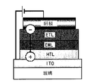
- FIG. 1 shows a schematic structural view of an OLED device.
- a transparent indium tin oxide (ITO) film is sputtered on the glass substrate as an anode, and a hole transport layer (HTL) and an electron transport layer (ETL) are formed on the anode, and a light-emitting layer formed of an organic substance is sandwiched between the hole transport layer Between the electron transport layer and the electron transport layer.
- a cathode layer is deposited on the electron transport layer.
- the transparent ITO film such as the highest occupied orbital level to the hole transport layer.
- electrons and holes such as electrons migrate to the light-emitting layer in the electron transport layer and the hole transport layer, thereby recombining with each other in the organic substance having the light-emitting property to form excitons in an excited state.
- the excitons transfer energy to the organic luminescent molecules and excite the electrons of the organic luminescent molecules from the ground state to the excited state.
- the photoelectron radiation is then deactivated to generate photons, release energy and return to a stable ground state.
- FIG. 2 illustrates a structural schematic diagram of an in-cell touch screen according to an example embodiment of the present disclosure.
- the in-cell touch panel includes an array substrate having a plurality of sub-pixels 01, each of the sub-pixels 01 includes an organic light emitting diode; a plurality of gate lines and data lines disposed on the array substrate that are crossed and insulated from each other (not shown in FIG.
- the gate line and the data line cross each other to define a plurality of sub-pixels; a plurality of self-capacitance electrodes 03 disposed in the same layer and independent of each other; and a plurality of touch lines connecting the respective self-capacitance electrodes to the touch detection chip 04 02, wherein the self-capacitance electrode 03 is disposed in the same layer as the anode of the organic light emitting diode.
- the self-capacitance electrode is connected to the touch detection chip 04 by the wire 02, and the drive signal Tx is applied to the self-capacitance electrode 03 through the touch detection chip 04, and the self-capacitance electrode 03 can receive the feedback signal by itself. Since the finger for operation is directly coupled in the course of work, the amount of touch change caused by the finger is relatively large.
- the anode of the organic light emitting diode is a discrete structure, each anode corresponds to one sub-pixel 01, and the self-capacitance electrode is disposed at a gap between adjacent anodes to form a grid pattern surrounding the anode of the organic light emitting diode.
- the self-capacitance electrode patterns t1-t4 include a row-column mesh structure formed between 6*3 sub-pixels 01, and t1-t4 are respectively connected to the touch detection through corresponding touch lines 02. Chip 04.
- the self-capacitance electrode is formed at the original gap, and the touch functionality can be realized on the basis of the existing array substrate preparation process without adding an additional process, thereby saving production cost and improving production efficiency.
- the sub-pixels are shown as rectangles of the same size in FIG. 2, those skilled in the art can design different shapes of the sub-pixels and the corresponding organic light-emitting diode anodes according to actual needs.
- the self-capacitance electrode may be disposed elsewhere in the layer where the anode of the organic light emitting diode is located, and is not limited to the gap between the anodes, and the pattern of the self-capacitance electrode is not limited to the grid pattern, but may be taken
- the anode of the organic light emitting diode is provided in any pattern in the same layer, such as a polygon, a ring, or the like.
- the cathode When the organic light emitting diode is a top emitting structure, the cathode is located at the top, thus shielding the self-capacitance electrode at the bottom. In order to eliminate the shielding effect, an opening may be provided in a region of the cathode of the organic light emitting diode that overlaps the self-capacitance electrode.
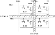
- Figure 3 illustrates a partial enlarged view of the in-cell touch screen of the circled portion shown in Figure 2.
- a portion (shaded portion) between four sub-pixels 1-4 of the self-capacitance electrode pattern t1 (FIG. 2) is illustrated, in which a plurality of gate lines and data which are disposed on the array substrate and which are insulated from each other and insulated from each other The line defines a plurality of sub-pixels.
- the human body capacitance acts on the self-capacitance of the self-capacitance electrode by direct coupling
- the capacitance of the self-capacitance electrode only under the touch position
- the value has a large amount of change, and the capacitance value of the other self-capacitance electrode adjacent to the self-capacitance electrode below the touch position is very small.
- the touch coordinates in the area where the self-capacitance electrode is located cannot be determined. Therefore, by setting the opposite sides of the adjacent two self-capacitance electrodes as the fold lines, the amount of change in the capacitance value of the self-capacitance electrode adjacent to the self-capacitance electrode located below the touch position can be increased.
- the macroscopic overall shape of the plurality of self-capacitance electrodes can be set as follows.
- the opposite sides of the adjacent two self-capacitance electrodes are arranged in a stepped shape, and the adjacent step shapes are uniform and match each other.
- Figure 4a shows 2*2 self-capacitance electrodes 03'.
- opposite sides of the adjacent two self-capacitance electrodes are disposed in a concavo-convex shape, and adjacent concavo-convex shapes are uniform and matched with each other.
- Fig. 4b shows 2*2 self-capacitance electrodes 03".
- self-capacitance electrodes are illustrated as squares having side sides of a polygonal line shape in Figs. 4a and 4b, this is merely an example, self-capacitance
- the electrodes may have other macroscopic overall shapes in which the opposite sides of adjacent self-capacitance electrodes 03 have a polygonal shape.
- adjacent self-capacitance electrodes are not in contact with each other.
- the density of the touch screen is usually on the order of millimeters. Therefore, the density and the occupied area of the self-capacitance electrode can be selected according to the required touch density to ensure the required touch density.
- the self-capacitance electrode can be designed as a square electrode of about 5 mm * 5 mm. Since the density of the display screen is usually on the order of micrometers, generally one self-capacitance electrode corresponds to a plurality of sub-pixels in the display screen.
- the touch detection chip is configured to determine the touch position by detecting a change in the capacitance value of each capacitor electrode during the touch time phase.
- the touch detection chip is prepared, for example, using an integrated circuit (IC).
- IC integrated circuit
- the arrangement of the touch lines can be adjusted according to a specific scheme.
- an embodiment of the present disclosure further provides a display device including the in-cell touch screen provided above.
- the display device may be a passive matrix organic light emitting diode (PMOLED) display, wherein the substrate requires an external driving circuit, or may be an active matrix organic light emitting diode (AMOLED) display, wherein the driving circuit and the display array are integrated on the same substrate.
- PMOLED passive matrix organic light emitting diode
- AMOLED active matrix organic light emitting diode
- the display device can be any product or component having a display function, such as a mobile phone, a tablet computer, a television, a display, a notebook computer, a digital photo frame, a watch, a navigator, and the like.
- the proposed display device realizes touch functionality based on a self-capacitance scheme based on the existing organic light emitting diode display device without affecting the pixel characteristics of the display device. Compared with the mutual capacitance scheme, the signal-to-noise ratio is greatly improved. .
Landscapes
- Engineering & Computer Science (AREA)
- General Engineering & Computer Science (AREA)
- Theoretical Computer Science (AREA)
- Physics & Mathematics (AREA)
- Human Computer Interaction (AREA)
- General Physics & Mathematics (AREA)
- Quality & Reliability (AREA)
- Computer Networks & Wireless Communication (AREA)
- Optics & Photonics (AREA)
- Microelectronics & Electronic Packaging (AREA)
- Electroluminescent Light Sources (AREA)
- Devices For Indicating Variable Information By Combining Individual Elements (AREA)
Abstract
一种内嵌式触摸屏,包括:具有多个子像素(01)的阵列基板,每个子像素(01)包括有机发光二极管;设置于阵列基板上的多条彼此交叉且彼此绝缘的栅线和数据线,栅线和数据线彼此交叉界定多个子像素(01);多个同层设置且相互独立的自电容电极(03);以及将各个自电容电极(03)连接至触控侦测芯片(04)的多条触控线(02),其中自电容电极(03)可以与有机发光二极管的阳极同层设置。还提供了包括上述内嵌式触摸屏的显示装置。
Description
本公开一般地涉及显示领域,并且更具体地涉及一种内嵌式触摸屏及有机发光二极管显示装置。
有机发光二极管(OLED)显示技术作为极具发展潜力的显示技术,与液晶显示(LCD)技术相比,由于采用各像素自主发光模式取代统一背光模式,因而具有可视角显著增大、功耗降低、对比度提高、屏幕厚度减薄、响应时间快,发光效率高等优点。
触摸屏功能已经成为现代输入方式的主要形式之一,在手机、平板计算机、电子书等便携式电子产品中,已经逐渐取代传统的机械按键输入方式,并且最终将实现全触摸无按键的输入模式。将触摸功能整合到显示装置中是目前的先进技术趋势。
触摸屏按照组成结构可以分为:外挂式触摸屏、覆盖表面式触摸屏以及内嵌式触摸屏。其中,外挂式触摸屏是将触摸屏与液晶显示屏分开生产,然后贴合到一起从而形成具有触摸功能的液晶显示屏。外挂式触摸屏存在制作成本较高、光透过率较低、模组较厚等缺点。而内嵌式触摸屏将触摸屏的触控电极内嵌在液晶显示屏内部,不仅可以减薄模组整体的厚度,还可以大大降低触摸屏的制作成本,因而受到各大面板厂商的青睐。
目前,现有的内嵌式触摸屏利用互电容或自电容的原理来检测手指触摸位置。以美国苹果公司的Iphone5为例,其采用基于互电容的内嵌式触摸屏,将电容电极制作在阵列基板上。相对于常规阵列工艺而言,该内嵌式触摸屏的阵列工艺额外增加至少两张掩模和至少两次光刻工艺步骤,因此导致制作成本的上升。
相比之下,自电容的原理是在触摸屏中设置多个同层设置且相互绝缘的自电容电极,当人体未触碰屏幕时,各自电容电极所承受的电容为某一固定值;当人体触碰屏幕时,对应的自电容电极所承受的电容为固定值叠加人体电容。触控侦测芯片在触控时间段通过检测各自电容电极的电容值变化可以判断出触控位置。由于人体电容可以作用
于全部自电容,相对于人体电容仅能作用于互电容中的投射电容,由人体碰触屏幕所引起的触控变化量会大于利用互电容原理制作出的触摸屏,因此相对于互电容的触摸屏,基于自电容的触摸屏能够有效提高触控信号的信噪比,从而提高触控感应的准确性。
发明内容
本公开的一个目的是克服以上缺点中的至少一些,并且提供一种改进的内嵌式触摸屏和显示装置。
根据本公开的一个方面,提供了一种内嵌式触摸屏,可以包括:具有多个子像素的阵列基板,每个子像素包括有机发光二极管;设置于阵列基板上的多条彼此交叉且彼此绝缘的栅线和数据线,栅线和数据线彼此交叉界定多个子像素;多个同层设置且相互独立的自电容电极;以及将各个自电容电极连接至触控侦测芯片的多条触控线,其中自电容电极可以与有机发光二极管的阳极同层设置。
本公开将触摸技术整合到OLED显示装置中,实现了OLED显示与触摸功能的集成化。所提出的显示装置在现有有机发光二极管显示装置的基础上基于自电容方案实现触摸功能性,同时不影响显示装置的像素特性。相比于互电容方案,信噪比有较大幅度提升。
根据本公开的示例性实施例,有机发光二极管的阳极可以为分立结构,每一个阳极对应于一个子像素,并且自电容电极可以设置在相邻的阳极之间的间隙处。
通过在阳极原有的间隙处形成自电容电极,可以在现有的阵列基板制备工艺的基础上实现触摸功能性,而不需要增加额外的工艺,因此可以节省生产成本,提高生产效率。
根据本公开的另一示例性实施例,自电容电极的图案可以被设计成以阳极为网孔的网格状图案。
根据本公开的又一示例性实施例,有机发光二极管可以为顶发光结构,其中有机发光二极管的阴极在与自电容电极重叠的区域中具有开口。通过设置开口,可以消除顶发光结构中的顶部上的阴极对与阳极同层设置的自电容电极的屏蔽影响,从而提高触摸的灵敏度。
根据本公开的另一示例性实施例,相邻的两个自电容电极相对的侧边可以为折线形状。
在本公开实施例提供的内嵌式触摸屏中,由于人体电容通过直接耦合的方式作用于自电容电极的自电容,因此,当人体触碰屏幕时,仅在触摸位置下方的自电容电极的电容值有较大的变化量,而与触摸位置下方的自电容电极相邻的其它自电容电极的电容值变化量非常小。这样,当在触摸屏上滑动时,不能确定自电容电极所在区域内的触控坐标。因此,通过将相邻的两个自电容电极相对的侧边均设置为折线,可以增大与位于触摸位置下方的自电容电极相邻的自电容电极的电容值变化量。
根据本公开的另一示例性实施例,相邻的两个自电容电极相对的侧边可以为一致且相互匹配的阶梯形状。
根据本公开的另一示例性实施例,相邻的两个自电容电极相对的侧边可以为一致且相互匹配的凹凸形状。
根据本公开的另一示例性实施例,自电容电极可以被设计成5mm*5mm的方形电极。
根据本公开的另一方面,提供了一种显示装置,包括以上所述的任一种内嵌式触摸屏。
根据本公开的示例性实施例,所述显示装置可以是无源矩阵有机发光二极管显示器或者有源矩阵有机发光二极管显示器。
本公开的这些和其它目的、特征和优点将会从结合附图对于本公开示例性实施例的以下详细描述中变得更为清楚明了,其中附图未必按照比例绘制。在附图中:
图1为有机发光二极管(OLED)器件的结构示意图;
图2为根据本公开的示例实施例的内嵌式触摸屏的结构示意图;
图3为图2所示的内嵌式触摸屏的局部放大视图;以及
图4a和图4b分别为本公开实施例所提供的内嵌式触摸屏中相邻的自电容电极的结构示意图。
以下将结合附图详细描述本公开的示例性实施例。附图是示意性的,并未按比例绘制,且只是为了说明本公开的实施例而并不意图限
制本公开的保护范围。在附图中,相同的附图标记表示相同或相似的部件。为了使本公开的技术方案更加清楚,本领域熟知的工艺步骤及器件结构在此省略。
图1示出OLED器件的结构示意图。在玻璃基板上溅射透明的氧化铟锡(ITO)膜作为阳极,并且在阳极上形成空穴传输层(HTL)和电子传输层(ETL),由有机物形成的发光层夹在空穴传输层与电子传输层之间。最后在电子传输层上沉积阴极层。当对器件施加适当的正向偏压时,电子和空穴克服界面能垒,经由阴极和阳极注入,电子由金属阴极注入到电子传输层的最低未占轨道能级,空穴由宽带隙的透明ITO膜诸如到空穴传输层的最高已占轨道能级。在外部电场的驱动下,诸如的电子和空穴在电子传输层和空穴传输层中向发光层迁移,从而在有发光特性的有机物质内相互复合,形成处于激发态的激子。激子将能量传递给有机发光分子,并且激发有机发光分子的电子从基态跃迁到激发态。然后激发光电子辐射失活,产生光子,释放能量并且回到稳定的基态。
图2图示了根据本公开的示例实施例的内嵌式触摸屏的结构示意图。所述内嵌式触摸屏包括具有多个子像素01的阵列基板,每个子像素01包括有机发光二极管;设置于阵列基板上的多条彼此交叉且彼此绝缘的栅线和数据线(在图2中未示出),栅线和数据线彼此交叉界定多个子像素;多个同层设置且相互独立的自电容电极03;以及将各个自电容电极连接至触控侦测芯片04的多条触控线02,其中自电容电极03与有机发光二极管的阳极同层设置。将自电容电极用导线02连接至触控侦测芯片04,通过触控侦测芯片04向自电容电极03施加驱动信号Tx,并且该自电容电极03可以自己接收反馈信号。由于在工作过程中,例如用于操作的手指采用直接耦合的方式,因此手指引起的触控变化量会比较大。
在图2中示意性地图示了4个自电容电极图案t1-t4。具体地,有机发光二极管的阳极为分立结构,每一个阳极对应于一个子像素01,并且自电容电极设置在相邻的阳极之间的间隙处,形成围绕有机发光二极管的阳极的网格状图案。如图2所示,自电容电极图案t1-t4包括形成在6*3个子像素01之间的行-列网状结构,并且t1-t4分别通过对应的触控线02连接到触控侦测芯片04。通过在有机发光二极管的阳极
原有的间隙处形成自电容电极,可以在现有的阵列基板制备工艺的基础上实现触摸功能性,而不需要增加额外的工艺,因此可以节省生产成本,提高生产效率。
还需要指出的是,尽管在图2中将子像素示出为尺寸相同的矩形,但是本领域技术人员可以根据实际需要设计子像素和对应的有机发光二极管阳极的不同形状。此外,自电容电极可以设置在有机发光二极管的阳极所在层中的其它地方,而不限于在阳极之间的间隙中,并且自电容电极的图案也不限于网格状图案,而是可以采取与有机发光二极管的阳极同层设置的任何图案,例如多边形、环形等等。
当有机发光二极管为顶发光结构时,阴极位于顶部处,因此会对其下方处的自电容电极产生屏蔽影响。为了消除该屏蔽影响,可以在有机发光二极管的阴极的与自电容电极重叠的区域中设置开口。
图3图示了图2中所示的圆圈部分的内嵌式触摸屏的局部放大视图。在图3中,示出自电容电极图案t1(图2)的四个子像素1-4之间的部分(阴影部分),其中设置于阵列基板上的多条彼此交叉且彼此绝缘的栅线和数据线界定多个子像素。
在本公开实施例提供的内嵌式触摸屏中,由于人体电容通过直接耦合的方式作用于自电容电极的自电容,因此,当人体触碰屏幕时,仅在触摸位置下方的自电容电极的电容值有较大的变化量,而与触摸位置下方的自电容电极相邻的其它自电容电极的电容值变化量非常小。这样,当在触摸屏上滑动时,不能确定自电容电极所在区域内的触控坐标。因此,通过将相邻的两个自电容电极相对的侧边均设置为折线,可以增大与位于触摸位置下方的自电容电极相邻的自电容电极的电容值变化量。
可以采用如下方式设置多个自电容电极的宏观整体形状。在图4a中,将相邻的两个自电容电极相对的侧边设置为阶梯形状,相邻的阶梯形状一致且相互匹配。图4a示出2*2个自电容电极03′。可替换地,在图4b中,将相邻的两个自电容电极相对的侧边均设置为凹凸形状,相邻的凹凸形状一致且相互匹配。图4b示出2*2个自电容电极03″。需要指出的是,虽然在图4a和4b中将自电容电极图示为具有折线形状的侧边的方形,但是这仅仅是示例,自电容电极可以具有其它宏观整体形状,其中相邻的自电容电极03的相对侧边具有折线形状。在图
4a和4b中,相邻的自电容电极并不相互接触。
一般地,触摸屏的密度通常在毫米级,因此,可以根据所需的触控密度选择自电容电极的密度和所占面积,以保证所需的触控密度。例如可以将自电容电极设计为5mm*5mm左右的方形电极。由于显示屏的密度通常在微米级,因此,一般一个自电容电极会对应显示屏中的多个子像素。
触控侦测芯片用于在触控时间阶段通过检测各自电容电极的电容值变化以判断触控位置。触控侦测芯片例如使用集成电路(IC)制备。另外,在具体实施过程中,可根据具体方案调整触控线的排布。
基于相同的公开构思,本公开实施例还提供了一种显示装置,包括以上所提供的内嵌式触摸屏。所述显示装置可以是无源矩阵有机发光二极管(PMOLED)显示器,其中基板需要外接驱动电路,或者可以是有源矩阵有机发光二极管(AMOLED)显示器,其中驱动电路和显示阵列集成在同一基板上。
该显示装置可以为:手机、平板电脑、电视机、显示器、笔记本电脑、数码相框、手表、导航仪等任何具有显示功能的产品或部件。所提出的显示装置在现有有机发光二极管显示装置的基础上基于自电容方案实现触摸功能性,同时不影响显示装置的像素特性。相比于互电容方案,信噪比有较大幅度提升。。
尽管已经参照附图详细地描述了本公开的示例性实施例,但是这样的描述应当被认为是说明性或示例性的,而不是限制性的;本公开并不限于所公开的实施例。上面以及权利要求中描述的不同实施例也可以加以组合。本领域技术人员在实施要求保护的本公开时,根据对于附图、说明书以及权利要求的研究,能够理解并实施所公开的实施例的其他变型,这些变型也落入本公开的保护范围内。
在权利要求中,词语“包括”并不排除其他部件或步骤的存在并且“一”或“一个”并不排除复数。在相互不同的从属权利要求中陈述了若干技术手段的事实并不意味着这些技术手段的组合不能有利地加以利用。
Claims (10)
- 一种内嵌式触摸屏,包括:具有多个子像素的阵列基板,每个子像素包括有机发光二极管;设置于阵列基板上的多条彼此交叉且彼此绝缘的栅线和数据线,栅线和数据线彼此交叉界定多个子像素;多个同层设置且相互独立的自电容电极;以及将各个自电容电极连接至触控侦测芯片的多条触控线,其中自电容电极与有机发光二极管的阳极同层设置。
- 根据权利要求1所述的内嵌式触摸屏,其中有机发光二极管的阳极为分立结构,每一个阳极对应于一个子像素,并且自电容电极设置在相邻的阳极之间的间隙处。
- 根据权利要求2所述的内嵌式触摸屏,其中自电容电极的图案被设计成围绕有机发光二极管的阳极的网格状图案。
- 根据权利要求1或2所述的内嵌式触摸屏,其中有机发光二极管为顶发光结构,其中有机发光二极管的阴极在与自电容电极重叠的区域中具有开口。
- 根据权利要求1或2所述的内嵌式触摸屏,其中相邻的两个自电容电极相对的侧边为折线形状。
- 根据权利要求5所述的内嵌式触摸屏,其中相邻的两个自电容电极相对的侧边为一致且相互匹配的阶梯形状。
- 根据权利要求5所述的内嵌式触摸屏,其中相邻的两个自电容电极相对的侧边为一致且相互匹配的凹凸形状。
- 根据权利要求1或2所述的内嵌式触摸屏,其中自电容电极被设计成5mm*5mm的方形电极。
- 一种显示装置,包括根据权利要求1-8中任一项的内嵌式触摸屏。
- 根据权利要求9的显示装置,其中所述显示装置为无源矩阵有机发光二极管显示器或者有源矩阵有机发光二极管显示器。
Priority Applications (2)
| Application Number | Priority Date | Filing Date | Title |
|---|---|---|---|
| US15/108,404 US20170147112A1 (en) | 2015-07-06 | 2015-12-31 | Embedded touch screen and organic light emitting diode display device |
| EP15871295.0A EP3321785B1 (en) | 2015-07-06 | 2015-12-31 | Embedded touch screen and organic light-emitting diode display device |
Applications Claiming Priority (2)
| Application Number | Priority Date | Filing Date | Title |
|---|---|---|---|
| CN201510389330.9A CN104915084B (zh) | 2015-07-06 | 2015-07-06 | 内嵌式触摸屏及有机发光二极管显示装置 |
| CN201510389330.9 | 2015-07-06 |
Publications (1)
| Publication Number | Publication Date |
|---|---|
| WO2017004960A1 true WO2017004960A1 (zh) | 2017-01-12 |
Family
ID=54084196
Family Applications (1)
| Application Number | Title | Priority Date | Filing Date |
|---|---|---|---|
| PCT/CN2015/100124 Ceased WO2017004960A1 (zh) | 2015-07-06 | 2015-12-31 | 内嵌式触摸屏及有机发光二极管显示装置 |
Country Status (4)
| Country | Link |
|---|---|
| US (1) | US20170147112A1 (zh) |
| EP (1) | EP3321785B1 (zh) |
| CN (1) | CN104915084B (zh) |
| WO (1) | WO2017004960A1 (zh) |
Families Citing this family (17)
| Publication number | Priority date | Publication date | Assignee | Title |
|---|---|---|---|---|
| US10133426B2 (en) * | 2015-06-18 | 2018-11-20 | X-Celeprint Limited | Display with micro-LED front light |
| CN104915084B (zh) * | 2015-07-06 | 2018-09-07 | 京东方科技集团股份有限公司 | 内嵌式触摸屏及有机发光二极管显示装置 |
| CN105045435B (zh) * | 2015-09-11 | 2018-03-30 | 京东方科技集团股份有限公司 | 一种内嵌式触摸屏及显示装置 |
| CN105260069B (zh) * | 2015-09-23 | 2018-09-11 | 京东方科技集团股份有限公司 | 一种自电容式触控显示面板及显示装置 |
| US10230048B2 (en) | 2015-09-29 | 2019-03-12 | X-Celeprint Limited | OLEDs for micro transfer printing |
| TWI590215B (zh) | 2016-07-11 | 2017-07-01 | 友達光電股份有限公司 | 顯示面板 |
| TWI607562B (zh) * | 2016-07-11 | 2017-12-01 | 友達光電股份有限公司 | 顯示面板 |
| CN107092400B (zh) * | 2017-06-27 | 2019-10-01 | 上海天马微电子有限公司 | 触控显示面板及包含其的触控显示装置 |
| CN107482040A (zh) * | 2017-08-14 | 2017-12-15 | 武汉华星光电半导体显示技术有限公司 | Oled触控显示面板及oled触控显示器 |
| CN108183121A (zh) * | 2017-12-15 | 2018-06-19 | 武汉华星光电半导体显示技术有限公司 | 柔性显示面板及其制作方法 |
| CN108878676A (zh) * | 2018-05-31 | 2018-11-23 | 武汉华星光电半导体显示技术有限公司 | 一种amoled薄膜封装结构及其制造方法 |
| CN111596780A (zh) * | 2019-02-20 | 2020-08-28 | 富泰华工业(深圳)有限公司 | 触控显示结构、智能设备及驱动方法 |
| CN115576453B (zh) * | 2019-03-21 | 2025-12-30 | 深圳曦华科技股份有限公司 | 触摸检测方法和触摸检测电路、触摸显示面板和电子设备 |
| CN111755486A (zh) * | 2020-06-16 | 2020-10-09 | 武汉华星光电半导体显示技术有限公司 | 一种触控屏及电子装置 |
| CN112631458A (zh) * | 2020-12-24 | 2021-04-09 | 苏州椒图电子有限公司 | 一种led触摸显示装置及其触控方法 |
| CN114093932B (zh) * | 2022-01-21 | 2022-04-22 | 威海艾迪科电子科技股份有限公司 | 一种集成电路封装结构及其制备方法 |
| FR3152691A1 (fr) * | 2023-09-01 | 2025-03-07 | Arnaud GOKOU | Procédé et système pour accéder à des ressources et services distants à partir d’un contenu audiovisuel disponible sur un équipement de télévision |
Citations (6)
| Publication number | Priority date | Publication date | Assignee | Title |
|---|---|---|---|---|
| CN101894856A (zh) * | 2009-05-22 | 2010-11-24 | 上海天马微电子有限公司 | 有机发光二极管显示屏 |
| US20120306812A1 (en) * | 2006-04-14 | 2012-12-06 | Ritdisplay Corporation | Top-emitting oled display having transparent touch panel |
| CN104020910A (zh) * | 2014-05-30 | 2014-09-03 | 京东方科技集团股份有限公司 | 一种内嵌式触摸屏及显示装置 |
| CN104020892A (zh) * | 2014-05-30 | 2014-09-03 | 京东方科技集团股份有限公司 | 一种内嵌式触摸屏及显示装置 |
| CN104679369A (zh) * | 2013-12-02 | 2015-06-03 | 三星显示有限公司 | 包括触摸传感器的柔性显示装置 |
| CN104915084A (zh) * | 2015-07-06 | 2015-09-16 | 京东方科技集团股份有限公司 | 内嵌式触摸屏及有机发光二极管显示装置 |
Family Cites Families (14)
| Publication number | Priority date | Publication date | Assignee | Title |
|---|---|---|---|---|
| US8508495B2 (en) * | 2008-07-03 | 2013-08-13 | Apple Inc. | Display with dual-function capacitive elements |
| JP2011237489A (ja) * | 2010-05-06 | 2011-11-24 | Toshiba Mobile Display Co Ltd | 有機el表示装置 |
| JP5789113B2 (ja) * | 2011-03-31 | 2015-10-07 | 株式会社Joled | 表示装置および電子機器 |
| US9400576B2 (en) * | 2011-07-19 | 2016-07-26 | Apple Inc. | Touch sensor arrangements for organic light-emitting diode displays |
| US9336723B2 (en) * | 2013-02-13 | 2016-05-10 | Apple Inc. | In-cell touch for LED |
| US10042489B2 (en) * | 2013-09-30 | 2018-08-07 | Synaptics Incorporated | Matrix sensor for image touch sensing |
| KR102177651B1 (ko) * | 2014-04-28 | 2020-11-12 | 엘지디스플레이 주식회사 | 표시장치 및 그 구동방법 |
| US9836165B2 (en) * | 2014-05-16 | 2017-12-05 | Apple Inc. | Integrated silicon-OLED display and touch sensor panel |
| CN104020909B (zh) * | 2014-05-30 | 2017-06-30 | 京东方科技集团股份有限公司 | 一种内嵌式触摸屏及显示装置 |
| CN104216564B (zh) * | 2014-09-01 | 2017-09-01 | 上海天马微电子有限公司 | 一种触摸屏、触摸显示面板及显示装置 |
| CN104716144B (zh) * | 2015-03-06 | 2018-02-16 | 京东方科技集团股份有限公司 | 阵列基板及其制作方法、显示装置 |
| CN104698700B (zh) * | 2015-04-01 | 2018-05-08 | 上海天马微电子有限公司 | 一种触控显示面板及显示装置 |
| KR101679977B1 (ko) * | 2015-05-29 | 2016-11-28 | 엘지디스플레이 주식회사 | 자기 정전용량식 터치 센서 일체형 표시장치와 그 제조방법 |
| US20160357286A1 (en) * | 2015-06-05 | 2016-12-08 | Innolux Corporation | Display device |
-
2015
- 2015-07-06 CN CN201510389330.9A patent/CN104915084B/zh active Active
- 2015-12-31 EP EP15871295.0A patent/EP3321785B1/en active Active
- 2015-12-31 US US15/108,404 patent/US20170147112A1/en not_active Abandoned
- 2015-12-31 WO PCT/CN2015/100124 patent/WO2017004960A1/zh not_active Ceased
Patent Citations (6)
| Publication number | Priority date | Publication date | Assignee | Title |
|---|---|---|---|---|
| US20120306812A1 (en) * | 2006-04-14 | 2012-12-06 | Ritdisplay Corporation | Top-emitting oled display having transparent touch panel |
| CN101894856A (zh) * | 2009-05-22 | 2010-11-24 | 上海天马微电子有限公司 | 有机发光二极管显示屏 |
| CN104679369A (zh) * | 2013-12-02 | 2015-06-03 | 三星显示有限公司 | 包括触摸传感器的柔性显示装置 |
| CN104020910A (zh) * | 2014-05-30 | 2014-09-03 | 京东方科技集团股份有限公司 | 一种内嵌式触摸屏及显示装置 |
| CN104020892A (zh) * | 2014-05-30 | 2014-09-03 | 京东方科技集团股份有限公司 | 一种内嵌式触摸屏及显示装置 |
| CN104915084A (zh) * | 2015-07-06 | 2015-09-16 | 京东方科技集团股份有限公司 | 内嵌式触摸屏及有机发光二极管显示装置 |
Non-Patent Citations (1)
| Title |
|---|
| See also references of EP3321785A4 * |
Also Published As
| Publication number | Publication date |
|---|---|
| CN104915084B (zh) | 2018-09-07 |
| CN104915084A (zh) | 2015-09-16 |
| EP3321785A4 (en) | 2019-01-23 |
| US20170147112A1 (en) | 2017-05-25 |
| EP3321785A1 (en) | 2018-05-16 |
| EP3321785B1 (en) | 2020-11-18 |
Similar Documents
| Publication | Publication Date | Title |
|---|---|---|
| CN104915084B (zh) | 内嵌式触摸屏及有机发光二极管显示装置 | |
| KR102876928B1 (ko) | 가시광 센서가 내장된 유기 발광 다이오드 디스플레이 패널 및 이를 포함하는 표시 장치 | |
| CN107819018B (zh) | 一种电致发光显示面板及显示装置 | |
| TWI809661B (zh) | 顯示裝置 | |
| US9836165B2 (en) | Integrated silicon-OLED display and touch sensor panel | |
| CN104393021B (zh) | 像素结构、透明触摸显示屏及其制作方法、和显示装置 | |
| TWI627570B (zh) | 具有內建觸控螢幕的有機發光顯示面板及有機發光顯示裝置 | |
| CN105045435B (zh) | 一种内嵌式触摸屏及显示装置 | |
| CN107871470B (zh) | 具有内置触摸屏的有机发光显示面板和有机发光显示装置 | |
| CN107104131B (zh) | 一种触控显示面板及显示装置 | |
| US10627963B2 (en) | Display device including touch sensor electrodes having a particular pitch | |
| KR102709760B1 (ko) | 표시장치 | |
| US9412796B2 (en) | High-accuracy OLED touch display panel structure | |
| CN107797687A (zh) | 显示面板、显示装置、集成驱动电路和驱动方法 | |
| CN108268168A (zh) | 具有集成触摸屏的显示装置及其制造方法 | |
| WO2022062879A1 (zh) | 触控基板及显示面板 | |
| CN106354302A (zh) | 内嵌式透明触控显示面板及其制造方法、驱动方法 | |
| CN107885400B (zh) | 一种oled触控显示面板及其驱动方法 | |
| CN104238815A (zh) | 一种显示面板及其驱动方法、显示装置 | |
| CN102830827A (zh) | 触控显示装置及其制造方法 | |
| CN205068332U (zh) | 内嵌显示触控结构 | |
| KR20170107803A (ko) | 터치 입력 장치 | |
| KR20170077910A (ko) | 자기 정전 용량형 터치 스크린 및 이를 구비하는 표시 장치 | |
| CN107146784A (zh) | 阵列基板和包括其的嵌入式触摸显示面板 | |
| KR102056929B1 (ko) | 터치스크린패널 일체형 표시장치 |
Legal Events
| Date | Code | Title | Description |
|---|---|---|---|
| REEP | Request for entry into the european phase |
Ref document number: 2015871295 Country of ref document: EP |
|
| WWE | Wipo information: entry into national phase |
Ref document number: 15108404 Country of ref document: US |
|
| 121 | Ep: the epo has been informed by wipo that ep was designated in this application |
Ref document number: 15871295 Country of ref document: EP Kind code of ref document: A1 |
|
| NENP | Non-entry into the national phase |
Ref country code: DE |
|
| WWE | Wipo information: entry into national phase |
Ref document number: 2015871295 Country of ref document: EP |