WO2017014094A1 - 窒化物半導体発光素子 - Google Patents
窒化物半導体発光素子 Download PDFInfo
- Publication number
- WO2017014094A1 WO2017014094A1 PCT/JP2016/070451 JP2016070451W WO2017014094A1 WO 2017014094 A1 WO2017014094 A1 WO 2017014094A1 JP 2016070451 W JP2016070451 W JP 2016070451W WO 2017014094 A1 WO2017014094 A1 WO 2017014094A1
- Authority
- WO
- WIPO (PCT)
- Prior art keywords
- layer
- electrode
- mesa
- metal layer
- nitride semiconductor
- Prior art date
- Legal status (The legal status is an assumption and is not a legal conclusion. Google has not performed a legal analysis and makes no representation as to the accuracy of the status listed.)
- Ceased
Links
Images







Classifications
-
- H—ELECTRICITY
- H10—SEMICONDUCTOR DEVICES; ELECTRIC SOLID-STATE DEVICES NOT OTHERWISE PROVIDED FOR
- H10H—INORGANIC LIGHT-EMITTING SEMICONDUCTOR DEVICES HAVING POTENTIAL BARRIERS
- H10H20/00—Individual inorganic light-emitting semiconductor devices having potential barriers, e.g. light-emitting diodes [LED]
- H10H20/80—Constructional details
- H10H20/81—Bodies
- H10H20/822—Materials of the light-emitting regions
- H10H20/824—Materials of the light-emitting regions comprising only Group III-V materials, e.g. GaP
- H10H20/825—Materials of the light-emitting regions comprising only Group III-V materials, e.g. GaP containing nitrogen, e.g. GaN
-
- H—ELECTRICITY
- H10—SEMICONDUCTOR DEVICES; ELECTRIC SOLID-STATE DEVICES NOT OTHERWISE PROVIDED FOR
- H10H—INORGANIC LIGHT-EMITTING SEMICONDUCTOR DEVICES HAVING POTENTIAL BARRIERS
- H10H20/00—Individual inorganic light-emitting semiconductor devices having potential barriers, e.g. light-emitting diodes [LED]
- H10H20/80—Constructional details
- H10H20/83—Electrodes
-
- H—ELECTRICITY
- H10—SEMICONDUCTOR DEVICES; ELECTRIC SOLID-STATE DEVICES NOT OTHERWISE PROVIDED FOR
- H10H—INORGANIC LIGHT-EMITTING SEMICONDUCTOR DEVICES HAVING POTENTIAL BARRIERS
- H10H20/00—Individual inorganic light-emitting semiconductor devices having potential barriers, e.g. light-emitting diodes [LED]
- H10H20/80—Constructional details
- H10H20/83—Electrodes
- H10H20/831—Electrodes characterised by their shape
-
- H—ELECTRICITY
- H10—SEMICONDUCTOR DEVICES; ELECTRIC SOLID-STATE DEVICES NOT OTHERWISE PROVIDED FOR
- H10H—INORGANIC LIGHT-EMITTING SEMICONDUCTOR DEVICES HAVING POTENTIAL BARRIERS
- H10H20/00—Individual inorganic light-emitting semiconductor devices having potential barriers, e.g. light-emitting diodes [LED]
- H10H20/80—Constructional details
- H10H20/83—Electrodes
- H10H20/832—Electrodes characterised by their material
Definitions
- the present invention relates to a group III nitride semiconductor light emitting device having an emission peak wavelength of ultraviolet rays.
- the present invention relates to a technique for suppressing a decrease in light emission efficiency of an element due to current concentration at a mesa structure end of the light emitting element.
- the present invention also relates to a wafer including the light emitting device configuration.
- FIG. 8A and 8B show a typical schematic structure of the group III nitride semiconductor light emitting device 41.
- FIG. 8A is a top view of the element
- FIG. 8B is a cross-sectional view taken along line AA of FIG. 8A.
- the group III nitride semiconductor light emitting device 41 includes a stacked body including an n-type layer 12, an active layer 13, and a p-type layer 14 on one surface side of the substrate 11 (hereinafter sometimes referred to as “laminated semiconductor layer”). And a mesa structure 15 formed in a part of the laminated semiconductor layer is known.
- the mesa structure 15 is formed by forming a laminated semiconductor layer including the n-type layer 12, the active layer 13, and the p-type layer 14 on one surface side of the substrate 11, and then removing a part of the laminated structure by etching or the like. A part of 12 is exposed.
- a mesa structure 15 is formed by leaving a plateau-like portion (also referred to as a mesa) including the active layer 13 and the p-type layer 14 (see Patent Document 1).
- An n-electrode 16 is formed on the exposed surface of the n-type layer 12, and a p-electrode 17 is formed on the surface of the p-type layer 14.
- the current flows between the p electrode and the n electrode. Since the current tends to flow through a low resistance path (usually the shortest path), the current is in the vicinity of the end of the mesa structure 15 (hereinafter sometimes referred to as “mesa end”) close to the n electrode and the p electrode. Concentrate on the flow. As a result, the current does not flow uniformly in the active layer 13 and uneven light emission occurs, resulting in a decrease in light emission efficiency.
- Patent Document 2 discloses an ultraviolet semiconductor in which a p-type layer or a high-resistance layer having a higher resistance than a p-electrode is formed on the surface of the p-type layer on the side close to the n-electrode along the shape of the p-type layer side. A light emitting device is disclosed.
- a high resistance layer is formed on a p-type layer near the mesa edge as in Patent Document 2, it is possible to suppress current concentration in a region near the mesa edge.
- Patent Document 3 discloses a semiconductor light emitting device in which a trench is formed between a p electrode and an n electrode. By forming the trench, the variation in the length of the current path flowing between the p electrode and the n electrode is reduced, and the current is prevented from concentrating on a specific portion. However, in order to sufficiently reduce the variation in the length of the current path, it is necessary to increase the depth of the trench.
- the n-type layer has a high Al composition, so that the specific resistance of the n-type layer is increased and current is concentrated in a region near the mesa edge. Almost flow, and it tends to cause a decrease in luminous efficiency. Therefore, it has been desired to develop a light emitting element that can suppress a decrease in light emission efficiency due to current concentration.
- the present invention provides a technique for suppressing a decrease in luminous efficiency by suppressing a current flowing between a p-electrode and an n-electrode from being concentrated in a region near the mesa edge in a semiconductor element having a mesa structure.
- the purpose is that.
- the present inventor thought that the above problem could be solved by adjusting the structure of the p-electrode, and conducted intensive studies.
- the group III nitride semiconductor device has a p-electrode (hereinafter sometimes referred to as “p-type electrode structure 30”) in which a first metal layer, a conductive layer, and a second metal layer are laminated in this order. And it discovered that the said subject could be solved by making the specific resistance of the said conductive layer higher than the specific resistance of the said 1st metal layer, and came to complete this invention.
- the first invention is a group III nitride semiconductor device including an active layer between an n-type layer and a p-type layer and having a mesa structure including the p-type layer, and is on the n-type layer.
- It is a group III nitride semiconductor device having a higher specific resistance.
- the thickness of the conductive layer is 0.05 ⁇ m or more and 20 ⁇ m or less, and the specific resistance of the conductive layer is 0.1 ⁇ 10 ⁇ 4 to 1.0 ⁇ 10 ⁇ 2. It is a group III nitride semiconductor device having ⁇ cm.
- a third invention is a group III according to the first or second invention, wherein the first metal layer is a layer in ohmic contact with the p-type layer, and is composed of a single metal or two or more metals. It is a nitride semiconductor device.
- the distance between the mesa end of the group III nitride semiconductor device and the outer periphery of the second metal layer is not less than 1/3 of the diffusion length L s. It is a certain group III nitride semiconductor device.
- the distance between at least the protrusion at the mesa end and the outer periphery of the second metal layer in the top view of the group III nitride semiconductor device is equal to 1 of the diffusion length L s .
- This is a group III nitride semiconductor device that is / 3 or more.
- a sixth invention provides a group III nitride semiconductor device according to the first to third inventions, wherein the distance between the mesa end of the group III nitride semiconductor device and the outer periphery of the second metal layer is 20 ⁇ m or more. It is.
- a seventh invention is the group III according to the first to third inventions, wherein the distance between at least the protrusion of the mesa end and the outer periphery of the second metal layer in the top view of the group III nitride semiconductor device is 20 ⁇ m or more. It is a nitride semiconductor device.
- the eighth invention is a group III nitride semiconductor light emitting device according to the first to seventh inventions, wherein the emission peak wavelength is 200 to 350 nm.
- a group III nitride semiconductor light emitting device having an emission peak wavelength of 200 to 350 nm has a high Al composition in the n-type layer, so that the specific resistance of the n-type layer increases, current concentration at the mesa edge tends to occur, and the luminous efficiency is improved. It tends to cause a decline. Therefore, the configuration of the present invention is suitable.
- a ninth invention is a wafer comprising a group III nitride semiconductor device having a mesa structure including an active layer between an n-type layer and a p-type layer and having the p-type layer, the group III
- the nitride semiconductor device is a wafer according to the first to seventh aspects of the invention.
- a tenth invention is a wafer including a configuration of a group III nitride semiconductor light emitting device having an mesa structure including an active layer between an n-type layer and a p-type layer, and including the p-type layer,
- the group nitride semiconductor light emitting device is a wafer according to the configuration of the eighth invention.
- the group III nitride semiconductor element has a p-electrode formed by laminating a first metal layer, a conductive layer, and a second metal layer in this order on a p-type layer.
- the resistance higher than the specific resistance of the first metal layer, the current flowing between the p electrode and the n electrode is prevented from being concentrated in the region near the mesa end.
- a group III nitride semiconductor light-emitting device in which current easily flows uniformly through the active layer, light emission unevenness is suppressed, and reduction in light emission efficiency is suppressed can be obtained.
- the first metal layer and the conductive layer are formed on the entire laminated surface of the mesa portion.
- the distance between the mesa end and the outer periphery of the second metal layer can be set to a predetermined value or more.
- the distance between the mesa end and the outer periphery of the second metal layer can be set to a predetermined value or more at all the mesa ends.
- the distance between a part of the mesa edge and the outer periphery of the second metal layer can be set to a predetermined value or more. If the distance between the mesa end and the outer periphery of the second metal layer is greater than or equal to a predetermined value at all the mesa ends, the area of the second metal layer is reduced, and the resistance of the current flowing between the p electrode and the n electrode The value may increase and the operating voltage may increase.
- the second metal layer can be formed widely, and the resistance of the current flowing between the p electrode and the n electrode It is possible to suppress an increase in value and suppress an increase in operating voltage.
- the distance between at least the protrusion at the mesa end and the outer periphery of the second metal layer can be set to a predetermined value or more.
- a predetermined value or more By increasing the distance between at least the protrusion of the mesa end and the outer periphery of the second metal layer to a predetermined value or more, an increase in operating voltage is suppressed, and the current flowing between the p electrode and the n electrode is near the mesa end. Concentration can be suppressed. As a result, the decrease in luminous efficiency is further suppressed, and the occurrence of quality defects can be reduced.
- an ultraviolet light-emitting element having an emission peak wavelength in the range of 200 to 350 nm has a higher Al composition than that of a light-emitting element having an emission peak wavelength exceeding 350 nm, for example, a light-emitting element in the visible light region.
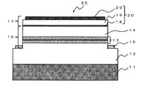
- FIG. 1 is a cross-sectional view of a group III nitride semiconductor device of the present invention.
- An example of a group III nitride semiconductor device viewed from above is shown.
- An example of a group III nitride semiconductor device viewed from above is shown.
- An example of a group III nitride semiconductor device viewed from above is shown.
- An example of a group III nitride semiconductor device viewed from above is shown.
- An example of a group III nitride semiconductor device viewed from above is shown.
- An example of a group III nitride semiconductor device viewed from above is shown.
- An example of a group III nitride semiconductor device viewed from above is shown.
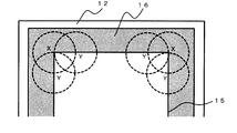
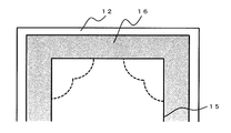
- a method for determining a “mesa edge protrusion” using a definition circle is shown. Various mesa end shapes are shown. A method for determining the second metal layer restriction region will be described. A method for determining the second metal layer restriction region will be described. The positional relationship between the mesa end of the element and the second metal layer is shown. The example of the positional relationship of a mesa edge and a 2nd metal layer is shown. The example of the positional relationship of a mesa edge and a 2nd metal layer is shown.
- An example of a typical group III nitride semiconductor light emitting device viewed from above is shown. 1 shows a cross-sectional view of a typical group III nitride semiconductor light emitting device. 3 shows a group III nitride semiconductor light-emitting device viewed from the top in Examples 1 to 3. FIG. 3 shows a group III nitride semiconductor light-emitting device viewed from above in Example 4.
- FIG. 1 shows a cross-sectional view of
- the light emitting region of light emitted from the group III nitride semiconductor light emitting device of the present invention is not particularly limited. According to the present invention, it is possible to suppress a decrease in light emission efficiency due to local current concentration in the mesa structure regardless of the light emission region.
- the present invention is applied to a group III nitride semiconductor light emitting device having an emission peak wavelength in the visible light region or the ultraviolet region. More preferably, the present invention is applied to a group III nitride semiconductor light emitting device that emits ultraviolet light having an emission peak wavelength of 200 to 350 nm.
- a group III nitride semiconductor light emitting device having an emission peak wavelength of 200 to 350 nm will be mainly described.
- a group III nitride semiconductor device 40 of the present invention includes a substrate 11, a mesa structure 15 (laminated semiconductor layer) including an n-type layer 12, an active layer 13 and a p-type layer 14, an n-electrode, 16 and a p-electrode 17.
- the p-type electrode structure 30 constituting the p-electrode 17 includes a first metal layer 18, a conductive layer 19, and a second metal layer 20. In the following, non-limiting examples of these will be described.
- the “mesa edge” is the outline of the mesa structure 15, which is the edge of the mesa structure in a top view, and is shown as the outer periphery (that is, the outline) of the p-type layer 14.
- the mesa structure is formed by etching the stacked semiconductor layer substantially vertically, but does not have to be completely vertical, and may be formed in a tapered shape from the top to the bottom of the mesa structure.
- the taper part is observed in a top view.
- the taper part is formed in an overhang shape, so that it is difficult to observe the top view.
- the mesa end is the end of the mesa structure 15 in a top view, and is defined as the outer periphery (that is, the contour) of the p-type layer 14 positioned at the uppermost layer of the mesa structure, and does not include the taper portion.
- the refractive index, the transmittance and the reflectance were based on light having a wavelength of 265 nm. This is because light of wavelength 265 nm is most suitable for sterilization because DNA has maximum absorption in the vicinity of wavelength 265 nm, and is considered to have high industrial utility value.
- the refractive index, the transmittance, and the reflectance are simply used, the values are for light with a wavelength of 265 nm.
- the substrate 11 is not particularly limited as long as it can epitaxially grow a group III nitride semiconductor crystal on the surface and transmits ultraviolet rays.
- Examples of the material used for the substrate 11 include sapphire, SiC (silicon carbide), AlN (aluminum nitride), Si (silicon), and the like. Among them, an AlN single crystal substrate having a c-plane as a main surface is preferable.
- the transmittance of the substrate 11 with respect to light having a wavelength of 265 nm is preferably as high as possible, preferably 50% or more, and more preferably 60% or more.
- the upper limit of the transmittance of the substrate 11 is preferably 100%, but the upper limit is 80% in consideration of industrial production.
- the transmittance of the substrate can be adjusted by the material, substrate thickness, crystallinity, and impurity content.
- the thickness of the substrate 11 is not particularly limited, but is preferably 30 to 1500 ⁇ m, more preferably 50 to 1000 ⁇ m. By setting the thickness of the substrate 11 in the above range, the transmittance is improved and the productivity is improved.
- the thickness of the substrate 11 only needs to satisfy the above range after the manufacture of the group III nitride semiconductor element, and the thickness of the substrate is obtained by grinding or polishing the lower surface of the substrate after laminating a laminated semiconductor layer and electrodes described later on the substrate. May be in the above range.
- the laminated semiconductor layer (the main part of the device including the mesa structure 15 in FIG. 1) is formed on the substrate 11 as shown in FIG. 1, and the n-type layer 12, the active layer 13, and the p-type layer 14 (p-type cladding layer). And a layer made of a p-type contact layer) are laminated in this order. Non-limiting examples are described below for each layer.
- Group III nitride semiconductor preferably containing impurities.
- the impurity concentration is 1.0 ⁇ 10 17 cm ⁇ 3 or more and 5.0 ⁇ 10 20 cm ⁇ 3 or less, preferably 1.0 ⁇ 10 18 cm ⁇ 3 or more and 5.0 ⁇ 10 19 cm ⁇ 3 or less.
- the refractive index of the n-type layer is not particularly limited, but is 1.5 to 3.0.
- the refractive index may be adjusted by the composition of the n-type layer.
- the thickness of the n-type layer is 100 nm or more and 10,000 nm or less, preferably 500 nm or more and 3000 nm or less.
- the group III nitride semiconductor device 40 includes a group III having the same or similar composition as AlN or the n-type layer between the substrate 11 and the n-type layer 12.
- a buffer layer including a nitride semiconductor may be included.
- a well layer having a band gap energy larger than that of the well layer (x, y, z are 0 ⁇ x ⁇ 1.0, 0 ⁇ y ⁇ 0.1, 0 ⁇ z ⁇ 1.0).
- the active layer may be a multiple quantum well structure or a single quantum well structure.
- the thickness of the well layer is 1 nm or more, preferably 2 nm or more, and the upper limit is 100 nm.
- the thickness of the barrier layer is 1 nm or more, preferably 2 nm or more, and the upper limit is 1 ⁇ m.
- Such an active layer can be manufactured by the MOCVD method.
- the p-type layer 14 includes a p-type cladding layer and a p-type contact layer.
- Group III nitride semiconductor preferably containing impurities.
- the impurity of the p-type cladding layer is preferably Mg.
- the impurity concentration in the p-type cladding layer is 1.0 ⁇ 10 17 cm ⁇ 3 or more and 5.0 ⁇ 10 20 cm ⁇ 3 or less, preferably 1.0 ⁇ 10 18 cm ⁇ 3 or more and 5.0 ⁇ 10 20 cm ⁇ . 3 or less.
- the thickness of the p-type cladding layer is 5 nm to 100 nm, preferably 10 nm to 80 nm.
- the p-type contact layer is made of GaN. If the p-type contact layer is made of GaN, that is, a p-GaN layer, the contact characteristics of the p-type contact layer can be improved.
- the p-type contact layer preferably contains an impurity.
- the impurity of the p-type contact layer is preferably Mg, like the p-type cladding layer.
- the impurity concentration in the p-type contact layer is 1.0 ⁇ 10 17 cm ⁇ 3 or more and 5.0 ⁇ 10 20 cm ⁇ 3 or less, preferably 1.0 ⁇ 10 18 cm ⁇ 3 or more and 2.0 ⁇ 10 20 cm ⁇ . 3 or less.
- the thickness of the p-type contact layer is 1 nm to 200 nm, preferably 5 nm to 50 nm. By setting the thickness of the p-type contact layer within the above range, the contact characteristics of the p-type layer are improved.
- the n electrode 16 is formed on the exposed surface of the n-type layer 12.
- the exposed surface of the n-type layer is formed by means such as etching.
- the stacked semiconductor layer remains in a plateau shape, and the mesa structure 15 is formed.
- the n-electrode on the n-type layer is formed along the lower end of the mesa structure in the low-level portion of the mesa structure, but is slightly spaced from the bottom of the mesa structure and is n-type between the mesa structure 15 and the n-electrode 16.
- the structure in which the layer 12 is exposed may be used.
- the n electrode 16 may be formed so as to surround the entire p electrode 17 along the mesa edge, and the n electrode may be formed so as to surround a part of the p electrode. May be.
- the p electrode may be formed so as to surround the n electrode.
- Etching techniques include dry etching such as reactive ion etching and inductively coupled plasma etching.
- the exposed surface is preferably surface-treated with an acid or alkali solution in order to remove etching damage.
- an n-type electrode 16 having ohmic properties is formed on the exposed surface of the n-type layer.
- the patterning of the n electrode can be performed using a lift-off method.
- a photoresist is applied to the surface on which the electrode is to be formed, irradiated with ultraviolet rays using a UV exposure machine equipped with a photomask, and immersed in a developer to dissolve the exposed photoresist to form a desired pattern.
- an electrode metal is deposited on the patterned photoresist, and the photoresist is dissolved with a stripping solution to form an electrode metal pattern.
- an electrode metal film is formed on the electrode formation surface, a photoresist is applied, the photoresist is patterned through an exposure and development process, and the electrode is formed by dry etching or wet etching using the photoresist as a mask.
- a method of patterning a metal and dissolving the photoresist with a stripping solution is preferable because the process is relatively simple.
- Examples of the method for depositing the n-electrode metal include vacuum deposition, sputtering, and chemical vapor deposition. In particular, vacuum deposition is preferable because impurities in the electrode metal can be eliminated.
- the material used for the n-electrode can be selected from known materials. For example, Ti, Al, Rh, Cr, In, Ni, Pt, Au, etc. are mentioned. Among these, Ti, Al, Rh, Cr, Ni, and Au are preferable. In particular, a combination of Ti, Al, and Au is preferable because it can improve ohmic properties and reflectivity.
- the n-electrode may be a single layer containing an alloy or oxide of these metals, or a multilayer structure.
- the thickness of the n-electrode is not particularly limited, but is preferably 2 nm or more in consideration of production stability, and the upper limit is 2 ⁇ m.
- the pattern of the n electrode is not particularly limited, and may be formed so as to surround the entire mesa structure 15 along the mesa edge (FIGS. 2A to 2F). It may be formed so as to surround a part of the structure 15 (FIG. 2G). Further, the n electrode may be formed so as to surround the p electrode (FIGS. 2A to E and G), and conversely, the p electrode may be formed so as to surround the n electrode (FIG. 2F).
- the width of the n electrode is not particularly limited, but is usually about 5 to 100 ⁇ m, preferably 10 to 50 ⁇ m.
- the width of the n electrode may not be uniform. For example, a narrow part and a wide part may be mixed. In this case, the average width of the n electrodes may be in the above range.
- heat treatment is performed at a temperature of 300 ° C. to 1100 ° C. for 30 seconds to 3 minutes.
- optimal conditions can be selected suitably according to the metal seed
- the p-electrode 17 of the present invention has a p-type electrode structure 30.
- the first metal layer 18, the conductive layer 19, and the second metal layer 20 are laminated in this order.
- the p-type electrode structure 30 in which the p-electrode 17 of the group III nitride semiconductor element is formed by laminating the first metal layer 18, the conductive layer 19, and the second metal layer 20 in this order It has been found that by having it, current concentration can be suppressed and a decrease in luminous efficiency can be suppressed.
- the current is applied to the second metal layer 20 and the first metal layer 20 in the p-type electrode structure constituting the p-electrode.
- An attempt is made to flow along a path with low resistance to the metal layer 18. Since the conductive layer 19 immediately below the second metal layer 20 has a higher specific resistance than the first metal layer 18 immediately below the conductive layer, the current is conducted through the conductive layer through the shortest path, and the first metal layer 18 is passed through. The tendency to flow increases.
- the conductive layer 19 having a high specific resistance is interposed between the second metal layer 20 and the first metal layer 18, the current is suppressed from being concentrated in a region near the mesa edge. It is possible to flow through the laminated semiconductor layer without concentration.
- the operating voltage does not increase excessively.
- the specific resistance value of the conductive layer 19 becomes close to the specific resistance value of the n-type layer 12 by increasing the specific resistance of the conductive layer 19.
- the value of the diffusion length L s in the n-type layer 12 increases, the electron diffusion distance in the n-type layer increases, and current concentration in the vicinity of the mesa edge in the n-type layer is suppressed. That is, due to the conductive layer 19 having a high specific resistance, current flows to the active layer 13 without being concentrated locally, and a decrease in light emission efficiency is suppressed.
- the present invention local concentration of current in the p-type electrode structure 30 can be suppressed.
- the current flowing between the p-electrode 17 and the n-electrode 16 having the p-type electrode structure 30 is also prevented from being concentrated in a region near the mesa end, and a decrease in luminous efficiency can be suppressed.
- the first metal layer 18, the conductive layer 19, and the second metal layer 20 that form the p-type electrode structure 30 will be described below.
- the first metal layer 18 is formed so as to be in ohmic contact with the p-type layer 14.
- the metal material used for the first metal layer 18 is preferably Ni, Au, Pt, Pd, Ru, Os, Rh, Ir, or Ag, and more preferably Ni, Au, Pt, or Pd. From these, a material having a specific resistance lower than that of the material constituting the conductive layer 19 described in detail below may be selected. In the first metal layer, these metals may be used alone or in combination of two or more.
- the first metal layer 18 may be a single layer containing an alloy or oxide of these metals or a multilayer structure.
- Specific resistance of the first metal layer 18 is preferably 1 ⁇ 10 -6 ⁇ 2 ⁇ 10 -5 ⁇ cm, more preferably 1 ⁇ 10 -6 ⁇ 1 ⁇ 10 -5 ⁇ cm.
- the specific resistance of the first metal layer 18 is lower than the specific resistance of the conductive layer 19 described later.
- the thickness of the first metal layer 18 is preferably 1 nm or more and 200 nm or less, more preferably 2 nm or more and 100 nm or less from the viewpoint of productivity.
- the patterning of the first metal layer 18 is preferably performed using a lift-off method, as is the patterning of the n-electrode.
- the shape and size of the first metal layer 18 are substantially similar to the mesa structure 15.
- the first metal layer 18 may be formed in a similar shape slightly smaller than the mesa structure 15.
- the first metal layer 18 is formed on the entire laminated surface of the p-type layer.
- the first metal layer 18 As a method for depositing the first metal layer 18, for example, vacuum deposition, sputtering, chemical vapor deposition, and the like can be cited as in the method for forming the n-electrode.
- vacuum deposition is preferable because impurities in the electrode metal can be eliminated.
- heat-treat at a temperature of 200 ° C. to 800 ° C. for 30 seconds to 3 minutes after depositing the metal. About the temperature and time of heat processing, optimal conditions can be suitably selected according to the metal seed
- the conductive layer 19 is formed on the first metal layer.
- the material used for the conductive layer 19 is preferably ZnO, ZnO doped with Al (hereinafter simply referred to as AZO), SnO 2 doped with Sb (hereinafter simply referred to as ATO), or ZnO with Ge.
- Doped hereinafter simply referred to as GZO
- oxide conductors are Ge, Si, and Ti, and more preferably ZnO, AZO, ITO, ATO, GZO, Ge, Si, and Ti.
- the specific resistance of the conductive layer 19 is preferably 0.1 ⁇ 10 ⁇ 4 to 1.0 ⁇ 10 ⁇ 2 ⁇ cm, more preferably 0.5 ⁇ 10 ⁇ 4 to 1.0 ⁇ 10 ⁇ 2 ⁇ cm. .
- the specific resistance of the conductive layer 19 is higher than the specific resistance of the first metal layer 18.
- the conductive layer 19 In the present invention, in order to suppress the current flowing in the conductive layer from being concentrated in a region near the mesa edge and to further suppress the excessive increase in the operating voltage, the conductive layer 19
- the specific resistance of the first metal layer 18 is preferably 2 to 1000 times, more preferably 4 to 1000 times, still more preferably 4 to 500 times, and more preferably 4 to 100 times. It is particularly preferable to do this.
- the thickness of the conductive layer 19 is preferably 0.05 ⁇ m or more and 20 ⁇ m or less, and more preferably 0.05 ⁇ m or more and 10 ⁇ m or less. If the thickness of the conductive layer is too large, the operating voltage may increase. If the thickness of the conductive layer is too small, it is difficult for the current to sufficiently spread within the conductive layer, and it may not be possible to effectively suppress the current from being concentrated in the region near the mesa edge.
- the shape and size of the conductive layer 19 are almost similar to the mesa structure 15.
- the conductive layer 19 may be formed in a similar shape slightly smaller than the mesa structure 15.
- the conductive layer 19 is formed on the entire surface of the first metal layer.
- the conductive layer is formed by vacuum deposition, sputtering, MBE, or the like.
- the second metal layer 20 is formed on the conductive layer.
- the metal material used for the second metal layer 20 is preferably Ti, Ni, Pt, Au, Mo, W, and more preferably Ti, Ni—, Pt, Au. In the second metal layer 20, these metals may be used alone or in combination of two or more. Further, the second metal layer 20 may be a single layer containing an alloy or oxide of these metals, or a multilayer structure.
- the specific resistance of the second metal layer 20 is not particularly limited. Usually, the specific resistance of metal is small compared to the specific resistance of the material used for the conductive layer. Among them, in order to exert an excellent effect, the specific resistance of the second metal layer 20 is preferably 1.0 ⁇ 10 ⁇ 6 ⁇ cm or more and 5.0 ⁇ 10 ⁇ 5 ⁇ cm or less, and 2.0 ⁇ 10 6 More preferably, it is ⁇ 6 ⁇ cm or more and 5.0 ⁇ 10 ⁇ 5 ⁇ cm or less.
- the thickness of the second metal layer 20 is preferably 0.05 ⁇ m or more and 10 ⁇ m or less, and more preferably 0.10 ⁇ m or more and 7 ⁇ m or less. If the thickness of the second metal layer is too large, the stress generated inside the second metal layer is increased, and the second metal layer may be easily peeled off. If the thickness of the second metal layer is too small, the heat dissipation is reduced, and solder may be easily diffused when used as a semiconductor element.
- the patterning of the second metal layer 20 is preferably carried out using a lift-off method, similarly to the patterning of the n-electrode.
- a method for depositing the second metal layer 20 as in the method for forming the n-electrode, for example, vacuum deposition, sputtering, chemical vapor deposition, or the like can be given.
- vacuum deposition is preferable because impurities in the electrode metal can be eliminated.
- the shape and size of the second metal layer 20 may be similar to the mesa structure 15 or may be completely different from the mesa structure.
- the formation position of the second metal layer 20 in the p-type electrode structure 30 can be set based on a predetermined guideline related to the shape of the mesa structure 15. Thereby, current concentration at the mesa end can be further suppressed.
- the shape of the second metal layer 20 is not particularly limited, but can be formed in a similar shape slightly smaller than the mesa structure 15.
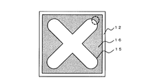
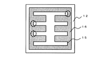
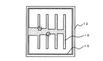
- the shape of the second metal layer 20 is a rectangular shape substantially similar to the mesa structure 15 shown in FIG. 2A, a cross shape as shown in FIGS. 2B and 2C, and as shown in FIGS. 2D to 2G. It may be comb-shaped.
- the width of the second metal layer is not particularly limited, but in the shape similar to the mesa structure 15 shown in FIGS. 2B to 2G, it is usually about 5 to 100 ⁇ m, preferably 10 to 50 ⁇ m.
- the width of the second metal layer may not be uniform. For example, a narrow part and a wide part may be mixed. In this case, the average width of the second metal layer may be in the above range.
- the p-electrode 17 is substantially similar to the mesa structure 15 on the p-type layer 14 positioned on the top of the plate-like mesa structure 15. Formed.
- the n-electrode 16 is formed in a lower low area as viewed from the mesa structure 15.
- a path with low resistance is given priority, so that the current is likely to be concentrated in a region near the end of the mesa structure 15 at the shortest distance between the n-electrode and the p-electrode.
- the group III nitride semiconductor device 40 of the present invention has a p-electrode 17 formed by laminating a first metal layer 18, a conductive layer 19, and a second metal layer 20 in this order in order to suppress current concentration at the mesa end. Furthermore, in a preferred embodiment of the present invention, the first metal layer 18 and the conductive layer 19 are formed over the entire laminated surface of the mesa portion, and the formation of the second metal layer 20 is to suppress current concentration at the mesa edge. A certain distance or more can be provided between the mesa end and the second metal layer 20.
- the distance between the outer periphery of the mesa edge and the second metal layer 20 and 1/3 or more of the diffusion length L s be able to.
- the distance between the mesa end and the outer periphery of the second metal layer 20 is the length of the shortest path from the arbitrarily selected mesa end to the contour of the second metal layer 20 in a top view.
- the distance between the outer periphery of the mesa end second metal layer is preferably 1/3 or more diffusion length L s, more preferably 1/3 or more of the diffusion length L s , 1.2 times the diffusion length L s or less, more preferably 1/3 or more of the diffusion length L s, is less than 1.0 times the diffusion length L s.
- the distance between the outer periphery of the mesa edge and the second metal layer 20 in all of the mesa edge may be 1/3 or more of the diffusion length L s.
- the distance between the outer periphery of the mesa edge and the second metal layer in all the mesa edge is preferably set to 1/3 or more of the diffusion length L s, more preferably diffusion length L s 1/3 or more, 1.2 times the diffusion length L s or less, more preferably 1/3 or more of the diffusion length L s, is less than 1.0 times the diffusion length L s.
- the distance between the outer periphery of the part of the mesa end the second metal layer may be more than one-third of the diffusion length L s. If the distance between the mesa end and the outer periphery of the second metal layer is 1/3 or more of the diffusion length L s at all the mesa ends, the area of the second metal layer is reduced, and the p electrode 17 and the n electrode 16 There is a risk that the resistance value of the current flowing between the two increases and the operating voltage increases.
- the second metal layer can be formed widely, and the p electrode and the n electrode It is possible to suppress an increase in the resistance value of the current flowing between them and suppress an increase in operating voltage.
- the distance between the outer periphery of the part of the mesa end the second metal layer is preferably 1/3 or more diffusion length L s, more preferably diffusion length L s of 1 / 3 or more, 1.2 times the diffusion length L s or less, more preferably 1/3 or more of the diffusion length L s, is less than 1.0 times the diffusion length L s.
- the distance between the outer layer 20 may be 1/3 or more of the diffusion length L s.
- the portion where current concentration is likely to occur refers to a portion where the p-electrode 17 protrudes into the n-electrode formation region in a top view.
- the portion since the p-electrode 17 is surrounded by the n-electrode 16, current tends to concentrate. As a result, the portion emits light more strongly, but the load is large and the deterioration tends to occur.
- the portion where current is concentrated emits light strongly, the light emission is weakened in other portions, so that uneven light emission occurs and the light emission efficiency tends to decrease.
- the second metal layer 20 of the p-type electrode structure constituting the p-electrode is formed on the mesa structure 15 in a shape substantially similar to the mesa structure, at least the mesa structure 15 is in the n-electrode formation region. If the distance between the mesa end and the second metal layer 20 is a predetermined value or more in the protruding portion, that is, the mesa end protrusion described in detail later, the current flowing from the second metal layer 20 is applied to the end of the mesa structure. It can flow to the conductive layer directly below without concentrating.
- the mesa structure 15 is an n-electrode.
- the distance between the at least projection and the outer periphery of the second metal layer 20 of the mesa edge is preferably set to 1/3 or more of the diffusion length L s, more preferably the diffusion length L s of 1/3 or more, 1.2 times the diffusion length L s or less, more preferably 1/3 or more of the diffusion length L s, is less than 1.0 times the diffusion length L s.
- the outer periphery n electrode of the second metal layer is less than 1/3 of the diffusion length L s It may be close by distance.
- ⁇ c contact resistance between p electrode / p-type layer and n electrode / n-type layer
- ⁇ p specific resistance of p-type layer
- ⁇ n specific resistance of n-type layer
- t p p-type layer Thickness
- t n the thickness of the n-type layer.
- the contact resistance is measured by a TLM (Transfer Length Method) method.
- a p-electrode pattern having a donut-shaped second metal layer non-formation region is formed on the surface of the p-GaN layer by a method similar to the method for manufacturing a semiconductor element (distance between electrodes: 5, 10, 20, 40 , 60, 80, 100 ⁇ m).
- the resistance value at each inter-electrode distance is measured, and the contact resistance between the p-electrode / p-type layer and the n-electrode / n-type layer is calculated from the relationship between the inter-electrode distance and the resistance value.
- the specific resistance of the p-type layer (p-GaN layer, p-AlGaN layer) and n-type layer (n-AlGaN layer) is calculated by measuring the Hall effect for the obtained sample.
- the diffusion length L s is the distance at which most electrons can diffuse in the n-type layer from the end of the n electrode near the mesa end to the mesa end in consideration of the movement of electrons to the p electrode. Point to.
- the diffusion length L s does not depend on the width of the electrode, it becomes a guideline for device design for suppressing current concentration even when the element is downsized and the electrode is thinned.
- the group III nitride semiconductor element has a p-electrode 17 formed by laminating the first metal layer 18, the conductive layer 19, and the second metal layer 20 in this order, Furthermore, although the distance between the mesa end and the outer periphery of the second metal layer 20 can be set to 1/3 or more of the diffusion length L s , in the present technology of the present invention, the mesa end and the second metal layer 20 It is sufficient that the distance from the outer periphery is 20 ⁇ m or more.
- the distance between the mesa edge and the outer periphery of the second metal layer 20 is preferably 20 ⁇ m or more, more preferably 20 to 80 ⁇ m, and even more preferably. Is 20 to 40 ⁇ m. From the viewpoint of further suppressing current concentration, the distance between the mesa edge and the outer periphery of the second metal layer 20 is preferably 20 ⁇ m or more at all mesa edges, more preferably 20 to 80 ⁇ m, and even more preferably 20 to 20 ⁇ m. 40 ⁇ m.
- the distance between a part of the mesa edge and the outer periphery of the second metal layer 20 is preferably 20 ⁇ m or more, more preferably 20 to 80 ⁇ m, still more preferably 20 to 40 ⁇ m. It is. From the viewpoint of suppressing current concentration and further suppressing increase in operating voltage, the distance between at least the protrusion at the mesa end and the outer periphery of the second metal layer 20 is preferably 20 ⁇ m or more, and more preferably 20 to 80 ⁇ m, more preferably 20 to 40 ⁇ m. This distance is sufficient for the current (2015) device design.
- the distance between the mesa end and the outer periphery of the second metal layer 20 may not be 20 ⁇ m or more.
- a guideline diffusion length L s it is sufficient to set the distance between the outer periphery of the mesa edge and the second metal layer 20.
- the group III nitride semiconductor device has a p-electrode 17 formed by laminating a first metal layer 18, a conductive layer 19, and a second metal layer 20 in this order, Between the mesa end and the second metal layer 20, a second metal layer restriction region in which the formation of the second metal layer is restricted can be provided. That is, in the preferred embodiment of the present invention may be present a second metal layer restricted area of more than 1/3 of the width or 20 ⁇ m or wider, the diffusion length L s in the vicinity of the end portion of the mesa structure.
- the second metal layer restriction region can be provided in the vicinity of all mesa edges.
- current concentration can be further suppressed, current can easily flow to the active layer, and light emission unevenness is suppressed. The decrease can be suppressed.
- the second metal layer restriction region can be provided in the vicinity of a part of the mesa end. If the second metal layer limiting region is provided in the vicinity of all the mesa edges, the area of the second metal layer is reduced, the resistance of the current flowing between the p electrode and the n electrode is increased, and the operating voltage is increased. May be.
- the second metal layer limiting region in the vicinity of a part of the mesa end, the second metal layer can be formed widely, and the resistance value of the current flowing between the p electrode and the n electrode increases. And an increase in operating voltage can be suppressed.
- the second metal layer limiting region can be provided at least in the vicinity of the protrusion at the mesa end. That is, in the preferred embodiment of the present invention, at least projections of the mesa edge, the second metal of more than 1/3 of the width or 20 ⁇ m or more of the width of the diffusion length L s between the mesa edge and the second metal layer 20
- the layer limiting region By providing the layer limiting region, an increase in operating voltage can be suppressed, and further, current does not easily flow in this region, so that current concentration in the vicinity of this region can be suppressed.
- the “projection at the end of the mesa” refers to a portion where the outline of the mesa structure 15 projects into the n-electrode formation region in a top view.
- the second metal layer is formed in this portion, electrons from the n electrode surrounding the periphery are concentrated on the second metal layer formed in the portion, and the active layer portion immediately below the second metal layer has a strong light.
- the light emitted from other parts is weak, and uneven light emission is likely to occur.
- the laminated semiconductor layer immediately below the second metal layer in the portion is likely to deteriorate.
- FIG. 2 shows a non-limiting example of the outline of the mesa structure 15 in the top view of the element and the formation pattern of the n electrode, and the “mesa end protrusion” where current tends to concentrate is indicated by a broken-line circle.
- the n-electrode 12 and the mesa structure 15 are in contact with each other.
- the mesa-structure taper portion is provided between the end of the mesa structure 15 and the n-electrode in the cross-section. Or an exposed n-type layer may be present.
- the formation of the second metal layer is limited to a region less than the predetermined distance.
- a second metal layer restriction region is provided.
- FIG. 2A shows an element structure in which a rectangular mesa structure 15 is formed in a top view.
- each vertex of the rectangle protrudes into the n-electrode formation region, and if the second metal layer 20 is formed in this portion, the current tends to concentrate on the mesa portion immediately below the second metal layer.
- FIG. 2B shows a cross-shaped mesa structure 15. Even in this structure, each vertex of the cross protrudes into the n-electrode formation region.
- FIG. 2C shows a mesa structure 15 with a rounded shape at the cross-shaped end. Even in this structure, the end of the cross projects into the n-electrode formation region.
- FIG. 2D shows a comb-like mesa structure 15.
- FIG. 2E is a modification of FIG. 2D and shows a structure in which the electrodes extend in a comb-teeth shape from the back of the comb.
- FIG. 2F shows a structure in which the n-electrode has a linear portion, and the electrode extends from the back of the comb forming the n-electrode.
- FIG. 2G shows a state in which a comb-shaped n-electrode surrounding the comb-shaped mesa structure is formed.
- the tips of the combs which are the second metal layer, and the vertices of the rectangles protrude into the n-electrode formation region.
- the pattern in the mesa structure formation pattern having the illustrated configuration and the similar configuration, the pattern is formed in a region less than a predetermined distance from the center of the circle indicating the “projection of the mesa end”.
- the bimetallic layer may be formed so as not to exist.
- the “projection at the mesa end” can be defined as a mesa portion in which an n electrode is excessively present around the group III nitride semiconductor device when viewed from the top. Therefore, in order to determine whether or not a “certain point” at the mesa end corresponds to a “projection at the mesa end”, the area of the n-electrode existing around the “certain point” may be considered. Specifically, a circle with a predetermined radius (hereinafter sometimes referred to as a “definition circle”) is drawn around the “certain point” to be determined, and the larger the area of the n electrode existing inside the circle, It is determined that the “certain point” is highly surrounded by the n electrode.
- a circle with a predetermined radius hereinafter sometimes referred to as a “definition circle”
- a circle having a predetermined radius is drawn around the “certain point” to be determined, and the smaller the area of the mesa portion (including the p-electrode) existing inside the circle, the “certain point” is n It can be said that the degree of being surrounded by the electrodes is high.
- the radius of the definition circle may be as long as the circle does not touch the other mesa edges. However, if the circle is too small, the area of the tapered portion between the mesa end and the n electrode or the exposed n-type layer area is overestimated, so it is necessary that the circle be larger than a certain size. That is, if the definition circle at the mesa end is too small, the area of the taper portion of the mesa portion and the area of the exposed n-type layer are overestimated in the definition circle, and the mesa portion (including the p electrode) and the n electrode The total area is relatively reduced, and appropriate evaluation cannot be performed.
- the center point an arbitrary point (the point to be determined) on the mesa edge, draw a circle of radius r n gradually increases.
- the radius of the circle is small, the relative ratio of the taper area and the n-electrode area is large, but as the circle increases, the relative ratio decreases, and the mesa part (including the p-electrode) and the n-electrode The area can be properly evaluated. Therefore, it is preferable that the radius of the circle in which the total area of the mesa portion (including the p electrode) and the n electrode in the circle is 80% of the total area of the circle is the radius of the “definition circle”. Note that the radius of the definition circle may be increased as long as the definition circle does not contact other mesa ends.
- a method for determining a “mesa end protrusion” using a definition circle will be described.
- a definition circle is drawn around a certain point on the mesa edge, a mesa portion (p electrode), an n-type layer, and an n electrode region exist in the definition circle, and the taper portion of the mesa structure in a top view May be observed.
- the above evaluation parameters are calculated from the area of the mesa portion, the area of the electrode, and the total area of the circle.
- the p-electrode is omitted.
- the first metal layer 18 and the conductive layer 19 are formed in the same shape as the mesa portion, and the second metal layer 20 is formed as the mesa portion. It can be formed in the same shape or smaller than this.
- FIG. 4 schematically shows a top view of mesa edges and n-electrodes of various contours.
- the n-type layer exposed between the electrodes and the tapered portion have a small area, and thus the illustration is omitted.
- the first metal layer and the conductive layer are formed in the same shape as the mesa portion, and the second metal layer is formed in a similar shape slightly smaller than the mesa portion. . That is, since the area of the p electrode is included in the area of the mesa portion, the illustration is omitted.
- the area of the mesa portion in the definition circle is smaller than the area of the n electrode. That is, although the evaluation parameter is smaller than that in the state A, the area of the n electrode is excessive, and current concentration is likely to occur in the p electrode and the active layer in this portion.
- the area of the mesa portion in the definition circle is smaller than the area of the n electrode. That is, the area of the n electrode is excessive, and current concentration tends to occur in the p electrode and the active layer in this portion.
- the area of the mesa portion in the definition circle is smaller than the area of the n electrode. That is, the area of the n electrode is excessive, and current concentration tends to occur in the p electrode and the active layer in this portion.
- the area of the mesa portion in the definition circle is larger than the area of the n electrode. That is, the evaluation parameter is less than 100%. Current concentration is less likely to occur in the p electrode and the active layer in this portion than in the state E.
- the area of the mesa structure in the definition circle is larger than the area of the n electrode. That is, the evaluation parameter is less than 100%. Current concentration is unlikely to occur in this portion of the p-electrode and the active layer.
- the second metal layer limiting region when the second metal layer limiting region is provided at least at the protrusion of the mesa end, the area of the n electrode is excessive with respect to the area of the mesa in the definition circle.
- the vicinity of the mesa edge as in each of the states A to D is defined as the second metal layer restriction region. That is, the vicinity of the mesa end having a large evaluation parameter is set as the second metal layer restriction region.
- a preferred embodiment in the case where the second metal layer limiting region is provided at least at the protrusion of the mesa end is as follows. Draw a definition circle with an arbitrary point on the mesa edge as the center point. When the evaluation parameter calculated by the area of each part in the definition circle exceeds 100%, it is determined that the center of the definition circle is located at the “projection at the mesa end”. If it is determined to be located on the protrusion of the mesa edge, a range where the center of the circle, the distance between the outer periphery of the second metal layer 20 becomes (or 20 ⁇ m in absolute distance) 1/3 or more of the diffusion length L s The second metal layer 20 is provided. In other words, the range from the center of the circle to less than 1/3 of the diffusion length L s (absolute distance is less than 20 ⁇ m) is the second metal layer restricted region.
- the evaluation parameter is approximately 300%. Therefore, the range of less than 1/3 of the diffusion length L s from the X point is a rectangular vertex (less than 20 ⁇ m in absolute distance) does not form a second metal layer. In the definition circle at the point Y in FIG. 5A (the mesa end located at the radius of the definition circle from the vertex X), the evaluation parameter is almost 100%.
- a limit point for forming the second metal layer is a circle whose radius is 1/3 of the diffusion length L s (absolute distance is 20 ⁇ m) from the Y point.
- L s absolute distance
- region second metal layer restricted area which is surrounded by the contour and dashed mesa It becomes.
- the distance from the X point and the Y point can be set to 20 ⁇ m or more to be the second metal layer restricted region.
- the second metal layer is not formed in all of the second metal layer restricted region, but the second metal layer is partially formed in the second metal layer restricted region. Even if formed, it is permissible as long as the object of the present invention is not impaired.
- the second metal layer may be formed in a portion that is far from the mesa end.
- the area where the formation of the second metal layer is restricted is preferably 90% or more, more preferably 98% or more, and further preferably 99% or more.
- the lower limit of the evaluation parameter is set to 100%, but these lower limits can be appropriately set according to the material of the laminated semiconductor layer (mesa structure portion), the operating environment of the element, and the requirements for the element. .
- the lower limit value of the allowable evaluation parameter can be lowered and the second metal layer restricted region can be widened.
- the evaluation parameter may be 80% or more, or 60% or more.
- the lower limit value of the evaluation parameter may be increased to narrow the second metal layer restriction region.
- the evaluation parameter may be 120% or more, or 140% or more.
- 20 ⁇ m can be used as a guideline for the radius of the definition circle for the current product. Further, as the electrodes become thinner in the future, appropriate evaluation is possible by reducing the radius of the definition circle. In this case as well, the circle is prevented from coming into contact with other mesa ends.
- the first metal layer and the conductive layer in the p-type electrode structure constituting the p electrode are formed on the entire surface of the mesa portion, and the formation of the second metal layer is predetermined from the “projection at the mesa end”.
- a second metal layer limiting region is provided within the range.
- the second metal layer can be formed in the mesa portion other than the second metal layer restriction region (hereinafter, sometimes referred to as “second metal layer allowable region”), There is no need to form a bimetallic layer.
- the 2nd metal layer should just be formed so that it may be conduct
- the outer peripheral shape of the second metal layer formed in the vicinity of the protrusion at the mesa end may be a rectangular shape, or may be an arc shape, an elliptical arc shape, a parabolic shape, or the like as shown in FIG.
- FIG. 6 shows an example in which a blank portion having a width of 5 ⁇ m is formed.
- the second metal layer may not be provided within a predetermined range from the “projection at the mesa end” where the evaluation parameter is equal to or greater than the specified value.
- the evaluation parameter indicating the degree of protrusion of the mesa portion continuously changes depending on the shape of the mesa end. Therefore, the distance from the mesa end to the second metal layer can be set according to the degree of protrusion of the mesa portion.
- the evaluation parameter value is high at point X (the mesa portion protrudes highly), it may be prohibited to form the second metal layer around this point (for example, within 20 ⁇ m).
- the evaluation parameter of the Y point is low, since it is difficult to occur even current concentration, the distance between the point Y and the second metal layer may alternatively less than 20 ⁇ m below 1/3 of the diffusion length L s.
- the distance between the second metal layer and the mesa end is more sufficient at the mesa end where the degree of protrusion to the n-electrode formation region is high, and the distance between the second metal layer and the mesa end at the mesa end where the degree of protrusion is low.
- the evaluation parameter may be determined at an arbitrary point on the mesa end, the “degree of protrusion” may be evaluated based on the result, and the width of the second metal layer limiting region from the mesa end may be set. .
- the second metal layer restriction region can be made wider at the mesa edge with a high evaluation parameter, and the second metal layer restriction region can be made narrower than the above definition at the mesa edge with a low evaluation parameter. For this reason, it is considered effective to define the second metal layer limited region using the absolute value or square value of the evaluation parameter.
- the distance from the vertex of the rectangle to the second metal layer is long in the longitudinal direction, and the second metal layer is from the midpoint of the rectangular short direction.
- the second metal layer can be provided so as to shorten the distance.
- the distance from the second metal layer is long from the apex and short from the midpoint in the longitudinal direction, and the distance changes continuously. The closer the midpoint is, the more gradually the distance changes.
- the end of the mesa and the end of the second metal layer may eventually coincide.
- the distance from the top of the arc (elliptical arc) to the second metal layer is long in the short direction.
- the second metal layer can be provided so that the distance from the mesa end to the second metal layer becomes shorter as the arc (elliptical arc) at the mesa end changes into a straight line.
- the distance to the second metal layer is long from the apex of the arc at the mesa end, is short from both ends of the arc, the distance changes continuously, and the distance changes gradually as it approaches both ends.
- the end of the mesa and the end of the second metal layer may eventually coincide.
- the lower surface of the light-transmitting substrate is ground or polished, whereby the thickness of the light-transmitting substrate can be reduced and the transmittance can be improved.
- a semiconductor element is manufactured by appropriately using a known semiconductor element separation method such as scribing, dicing, or laser fusing.
- Example 1 A laminated semiconductor layer having the cross-sectional structure shown in FIG. 1 was formed. First, an Al 0.7 Ga 0.3 N layer (thickness) doped with Si in an amount of 1.0 ⁇ 10 19 [cm ⁇ 3 ] on a C-plane AlN substrate (side 7 mm square, thickness 500 ⁇ m) by MOCVD. 1 ⁇ m) was formed as an n-type semiconductor layer. On this n-type layer, an active layer having a quantum well structure (well layer: thickness 2 nm, barrier layer: thickness 7 nm) was formed.
- the composition of the well layer and the barrier layer is Al 0.5 Ga 0.5 N and Al 0.7 Ga 0.3 N, respectively, and the barrier layer has 1.0 ⁇ 10 18 [cm ⁇ 3 ] Si. Doped.
- the active layer has a laminated structure of three well layers and four barrier layers.
- an AlN layer (thickness: 15 nm) doped with 5 ⁇ 10 19 [cm ⁇ 3 ] of Mg was formed as an electron blocking layer on the active layer.
- an Al 0.8 Ga 0.2 N layer (thickness: 50 nm) doped with 5 ⁇ 10 19 [cm ⁇ 3 ] Mg was formed as a p-type cladding layer on the electron block layer.
- a GaN layer (thickness: 100 nm) doped with 2 ⁇ 10 19 [cm ⁇ 3 ] of Mg was formed as a p-type contact layer on the p-type cladding layer.
- the obtained semiconductor wafer was heat-treated in N 2 at 900 ° C. for 20 minutes. Then, after forming a predetermined metal mask pattern on the surface of the p-type contact layer by photolithography and vacuum deposition, dry etching the p-type contact layer surface on which no pattern is formed until the n-type layer is exposed, A cross-shaped mesa structure having rounded ends as shown in FIG. 1C was formed.
- a Ni (thickness 20 nm) / Au (thickness 50 nm) layer is formed as a first metal layer on the p-type contact layer, and the first metal layer is baked at 550 ° C. for 3 minutes in an oxygen atmosphere. Formed.
- a Ti layer (thickness 500 nm) is formed as a conductive layer on the first metal layer, and Ti (thickness 20 nm) / Ni (thickness 400 nm) / Au (as a second metal layer is further formed on the Ti layer as the conductive layer. Thickness 135 nm) was laminated. As shown in FIG. 9A, the distance between the mesa end and the outer periphery of the second metal layer was 40 ⁇ m at all the mesa ends.
- the obtained semiconductor wafer was cut into a 750 ⁇ m square to obtain a group III nitride semiconductor light emitting device.
- the specific resistance of the Ti layer as the conductive layer was 0.5 ⁇ 10 ⁇ 4 ⁇ cm
- the specific resistance of the first metal layer was 1.0 ⁇ 10 ⁇ 5 ⁇ cm.
- the obtained group III nitride semiconductor light-emitting device emitted light uniformly when energized, and the emission wavelength was 265 nm when 150 mA was energized.
- Example 2 A group III nitride semiconductor light-emitting device was fabricated in the same manner as in Example 1, except that the conductive layer in Example 1 was changed from the Ti layer to the ITO layer. At this time, the specific resistance value of the ITO layer as the conductive layer was 4.0 ⁇ 10 ⁇ 4 ⁇ cm, and the specific resistance value of the first metal layer was 1.0 ⁇ 10 ⁇ 5 ⁇ cm. The obtained group III nitride semiconductor light-emitting device emitted light uniformly when energized, and the emission wavelength was 265 nm when 150 mA was energized.
- Example 3 A group III nitride semiconductor light-emitting device was fabricated in the same manner as in Example 1, except that the conductive layer in Example 1 was changed from the Ti layer to the AZO layer. At this time, the specific resistance value of the AZO layer as the conductive layer was 2.3 ⁇ 10 ⁇ 4 ⁇ cm, and the specific resistance value of the first metal layer was 1.0 ⁇ 10 ⁇ 5 ⁇ cm. The obtained group III nitride semiconductor light-emitting device emitted light uniformly when energized, and the emission wavelength was 265 nm when 150 mA was energized.
- Example 4 In Example 3, as shown in FIG. 9B, the distance between the mesa end and the outer periphery of the second metal layer is 40 ⁇ m only in the portion where the mesa end protrudes, and in the other portion, the mesa end and the second metal A group III nitride semiconductor light-emitting device was fabricated in the same manner as in Example 1 except that the distance from the outer periphery of the layer was less than 20 ⁇ m.
- the specific resistance value of the AZO layer was 2.3 ⁇ 10 ⁇ 4 ⁇ cm, and the specific resistance value of the first metal layer was 1.0 ⁇ 10 ⁇ 5 ⁇ cm.
- the obtained group III nitride semiconductor light-emitting device emitted light uniformly when energized, and the emission wavelength was 265 nm when 150 mA was energized.
- Example 1 a Group III nitride semiconductor light-emitting device was produced in the same manner as in Example 1, except that the conductive layer was not provided and the second metal layer was formed directly on the first metal layer.
- the obtained group III nitride semiconductor light emitting device emitted strong light near the mesa edge when energized, but light emission was weak in other portions, and there was uneven light emission.
Landscapes
- Led Devices (AREA)
Abstract
【課題】 メサ構造を有する半導体素子において、p電極とn電極との間に流れる電流がメサ端付近の領域に集中するのを抑制することにより、発光効率の低下を抑制する技術を提供する。 【解決手段】 n型層とp型層との間に活性層を含み、前記p型層を含むメサ構造を有するIII族窒化物半導体素子であって、前記n型層上にn電極、前記p型層上に、第一金属層、導電層、および第二金属層がこの順に積層されているp電極を有し、前記導電層の比抵抗が、前記第一金属層の比抵抗よりも高いIII族窒化物半導体素子。
Description
本発明は、紫外線の発光ピーク波長を有するIII族窒化物半導体発光素子に関する。特に、発光素子のメサ構造端部における電流集中に起因する素子の発光効率の低下を抑制する技術に関する。また、本発明は該発光素子構成を含むウエハに関する。
図8A、図8BにIII族窒化物半導体発光素子41の典型的模式構造を示す。図8Aは、素子の上面図であり、図8Bは図8AのA-A線断面図である。III族窒化物半導体発光素子41としては、基板11の一表面側にn型層12、活性層13およびp型層14を含む積層体(以下、「積層半導体層」と記載することがある)が形成され、その積層半導体層の一部にメサ構造15を形成したものが知られている。メサ構造15は、基板11の一表面側にn型層12、活性層13およびp型層14を含む積層半導体層を形成した後に、エッチング等により積層構造の一部を除去し、n型層12の一部を露出させて形成される。活性層13およびp型層14を含む台地状の部分(メサとも呼ばれる)を残存させることによりメサ構造15が形成される(特許文献1参照)。露出したn型層12の表面にはn電極16が形成され、p型層14の表面にはp電極17が形成される。
メサ構造15を有するIII族窒化物半導体発光素子41において、p型層上のp電極17およびn型層上のn電極16に動作電圧を印加すると、電流はp電極とn電極との間で抵抗の低い経路(通常は最短経路)を流れようとするため、電流はn電極およびp電極に近接するメサ構造15の端部(以下、「メサ端」と記載することがある)付近の領域に集中して流れる。この結果、電流が活性層13に均一に流れずに発光ムラが生じて、発光効率が低下する。
特許文献2には、p型層もしくはp電極よりも高抵抗の高抵抗層が、p型層の表面においてn電極に近い側でp型層側の形状に沿った形状に形成された紫外半導体発光素子が開示されている。特許文献2のように、メサ端に近いp型層上に高抵抗層を形成すると、メサ端付近の領域に電流が集中するのを抑制できる。
特許文献3には、p電極とn電極との間にトレンチが形成された半導体発光素子が開示されている。トレンチを形成することにより、p電極とn電極との間に流れる電流経路の長さのバラツキを減少させ、特定の部分に電流が集中するのを抑制する。しかし、電流経路の長さのバラツキを十分に小さくするには、トレンチの深さを大きくする必要がある。
近年のデバイス設計の多様化により、様々な形状、構成の発光素子が提案され、メサ構造、電極形状のデザインも多様化している。そのため、上記のような高抵抗層の形成、トレンチの形成などの技術は、発光素子の製造における工程数の増加を招き、製造がより煩雑になるため、多様化したメサ構造、電極形状に迅速に対応することが困難になっている。
そして、特に、発光ピーク波長が200~350nmである深紫外の発光素子では、n型層のAl組成が高いためn型層の比抵抗が増大して、電流がメサ端付近の領域に集中して流れやすくなり、発光効率の低下を招きやすい。そのため、電流集中に起因する発光効率の低下を抑制できる発光素子の開発が望まれていた。
本発明は、メサ構造を有する半導体素子において、p電極とn電極との間に流れる電流がメサ端付近の領域に集中するのを抑制することにより、発光効率の低下を抑制する技術を提供することを目的としている。
本発明者は、p電極の構造を調整することにより、上記課題が解決できるのではないかと考え、鋭意検討した。そして、III族窒化物半導体素子が第一金属層、導電層、および第二金属層をこの順に積層してなるp電極(以下、「p型電極構造30」と記載することがある)を有し、前記導電層の比抵抗を前記第一金属層の比抵抗よりも高くすることにより、上記課題を解決できることを見出し、本発明を完成するに至った。
すなわち、第1の発明は、n型層とp型層との間に活性層を含み、前記p型層を含むメサ構造を有するIII族窒化物半導体素子であって、前記n型層上にn電極、前記p型層上に、第一金属層、導電層、および第二金属層がこの順に積層されているp電極を有し、前記導電層の比抵抗が、前記第一金属層の比抵抗よりも高いIII族窒化物半導体素子である。
第2の発明は、第1の発明において、前記導電層の厚みが0.05μm以上20μm以下であって、前記導電層の比抵抗が0.1×10⁻⁴~1.0×10⁻²ΩcmであるIII族窒化物半導体素子である。
第3の発明は、第1または第2の発明において、前記第一金属層が、前記p型層にオーミック接触する層であり、単一のあるいは2種以上の金属により構成される、III族窒化物半導体素子である。
第4の発明は、第1~3の発明において、前記III族窒化物半導体素子の上面視におけるメサ端と前記第二金属層の外周との距離が、拡散長Lsの1/3以上であるIII族窒化物半導体素子である。
第5の発明は、第1~3の発明において、前記III族窒化物半導体素子の上面視におけるメサ端の少なくとも突部と前記第二金属層の外周との距離が、拡散長Lsの1/3以上であるIII族窒化物半導体素子である。
第6の発明は、第1~3の発明において、前記III族窒化物半導体素子の上面視におけるメサ端と前記第二金属層の外周との距離が、20μm以上であるIII族窒化物半導体素子である。
第7の発明は、第1~3の発明において、前記III族窒化物半導体素子の上面視におけるメサ端の少なくとも突部と前記第二金属層の外周との距離が、20μm以上であるIII族窒化物半導体素子である。
第8の発明は、第1~7の発明において、発光ピーク波長が200~350nmのIII族窒化物半導体発光素子である。発光ピーク波長が200~350nmのIII族窒化物半導体発光素子は、n型層のAl組成が高いためn型層の比抵抗が増大して、メサ端への電流集中が生じやすく、発光効率の低下を招きやすい。そのため、本発明の構成が適している。
第9の発明は、n型層とp型層との間に活性層を含み、前記p型層を含むメサ構造を有するIII族窒化物半導体素子の構成を含むウエハであって、前記III族窒化物半導体素子の構成が前記第1~7の発明の構成であるウエハである。
第10の発明は、n型層とp型層との間に活性層を含み、前記p型層を含むメサ構造を有するIII族窒化物半導体発光素子の構成を含むウエハであって、前記III族窒化物半導体発光素子の構成が前記第8の発明の構成であるウエハである。
本発明では、III族窒化物半導体素子が、p型層上に第一金属層、導電層、および第二金属層をこの順に積層してなるp電極を有しており、前記導電層の比抵抗を、前記第一金属層の比抵抗よりも高くすることにより、p電極とn電極との間に流れる電流がメサ端付近の領域に集中するのを抑制する。その結果、電流が活性層に均一に流れやすくなって発光ムラが抑制され、発光効率の低下が抑制されたIII族窒化物半導体発光素子が得られる。
また、本発明では、p電極を構成するp型電極構造30において前記第一金属層および前記導電層はメサ部の積層面の全面に形成され、前記第二金属層の形成については、III族窒化物半導体素子を上面視から見た場合に、メサ端と前記第二金属層の外周との距離を所定値以上とすることができる。メサ端と前記第二金属層の外周との距離を所定値以上とすることで、p電極とn電極との間に流れる電流がメサ端付近の領域に集中するのをさらに抑制することができ、発光効率の低下を抑制することができる。
また、本発明では、全てのメサ端において、メサ端と前記第二金属層の外周との距離を所定値以上とすることができる。全てのメサ端において、メサ端と前記第二金属層の外周との距離を所定値以上とすることにより、電流集中をより一層抑制することができる。
さらに、本発明において、メサ端の一部と前記第二金属層の外周との距離を所定値以上とすることができる。全てのメサ端において、メサ端と前記第二金属層の外周との距離を所定値以上とすると、第二金属層の面積が小さくなって、p電極とn電極との間に流れる電流の抵抗値が増大し、動作電圧が増大することがある。メサ端の一部と前記第二金属層の外周との距離を所定値以上とすることで、第二金属層を広く形成することができ、p電極とn電極との間に流れる電流の抵抗値が増大するのを抑制し、動作電圧の増大を抑制できる。
動作電圧の増大をより一層抑制する観点から、本発明において、メサ端の少なくとも突部と前記第二金属層の外周との距離を所定値以上とすることができる。メサ端の少なくとも突部と前記第二金属層の外周との距離を所定値以上とすることで、動作電圧の増大を抑制し、p電極とn電極との間に流れる電流がメサ端近傍に集中するのを抑制できる。その結果、発光効率の低下がより抑制されて、品質不良の発生を低減することができる。
特に、200~350nmに発光ピーク波長を有する紫外発光素子では、350nmを超える発光ピーク波長の発光素子、例えば、可視光領域の発光素子と比べて、n型層のAl組成が高いためn型層の比抵抗が増大して、電流がメサ端付近の領域に集中しやすく、発光効率の低下を招きやすい。そのため、200~350nmに発光ピーク波長を有する紫外発光素子の構成として、本発明の構成が適している。
以下、本発明の実施の形態について適宜図面を参照して説明する。ただし、以下に説明する半導体素子は、本発明の技術思想を具体化した一例であって、本発明を限定しない。たとえば、以下に記載されている構成要素の寸法、材質、形状、その相対的配置等は特定的な記載がない限りは、本発明の範囲をそれのみに限定する趣旨ではなく、単なる説明例にすぎない。なお、各図面が示す部材の大きさや位置関係等は、説明を明確にするため誇張していることがある。
本発明のIII族窒化物半導体発光素子が放出する光の発光領域は、特に制限されるものではない。本発明によれば、発光領域に関係なく、メサ構造における局所的な電流集中による発光効率の低下を抑制することができる。好ましくは、本発明は、可視光領域、又は紫外領域に発光ピーク波長を有するIII族窒化物半導体発光素子に適用される。より好ましくは、本発明は、発光ピーク波長200~350nmの紫外線を放出するIII族窒化物半導体発光素子に適用される。以下、発光ピーク波長が200~350nmのIII族窒化物半導体発光素子を中心に説明する。
本発明のIII族窒化物半導体素子40は、図1に示すように、基板11と、n型層12、活性層13およびp型層14を含むメサ構造15(積層半導体層)と、n電極16と、p電極17とを含む。p電極17を構成するp型電極構造30は、第一金属層18、導電層19および第二金属層20からなる。以下に、これらについて非限定的な例を説明する。
なお、「メサ端」とは、メサ構造15の輪郭であり、メサ構造の上面視における端部であって、p型層14の外周(すなわち輪郭)として示される。メサ構造は、積層半導体層をほぼ垂直にエッチングして形成されるが、完全に垂直である必要はなく、メサ構造上部から下部にかけて、テーパ状に形成されていてもよい。メサ構造上部の面積がメサ構造下部の面積よりも小さい場合には、テーパ部は上面視により観察される。メサ構造上部の面積がメサ構造下部の面積よりも大きい場合には、テーパ部はオーバーハング状に形成されるため、上面視では観察が難しくなる。
以下の説明では、メサ端とは、上面視におけるメサ構造15の端部であり、メサ構造の最上層に位置するp型層14の外周(すなわち輪郭)と定義し、テーパ部は含めない。
また、屈折率、透過率および反射率は、波長265nmの光を基準とした。これは、DNAが波長265nm付近で極大吸収を持つことから波長265nmの光は殺菌に最も適しており、産業上の利用価値が高いと考えられるからである。以下、単に、屈折率、透過率、および反射率とした場合には、波長265nmの光に対する値である。
<基板>
基板11は、III族窒化物半導体結晶を表面にエピタキシャル成長でき、紫外線を透過する基板であれば特に限定されるものではない。基板11に用いられる材料としては、例えば、サファイア、SiC(炭化ケイ素)、AlN(窒化アルミニウム)、Si(シリコン)などが挙げられる。中でもc面を主面とするAlN単結晶基板が好ましい。
基板11は、III族窒化物半導体結晶を表面にエピタキシャル成長でき、紫外線を透過する基板であれば特に限定されるものではない。基板11に用いられる材料としては、例えば、サファイア、SiC(炭化ケイ素)、AlN(窒化アルミニウム)、Si(シリコン)などが挙げられる。中でもc面を主面とするAlN単結晶基板が好ましい。
基板11の波長265nmの光に対する透過率は、高ければ高いほど良く、好ましくは50%以上であり、より好ましくは60%以上である。基板11の透過率の上限は、好ましくは100%であるが、工業的な生産を考慮すると上限は80%である。基板の透過率は、材質、基板の厚み、結晶性、不純物含有量によって調整できる。
基板11の厚みは、特に制限されるものではないが、好ましくは30~1500μmであり、より好ましくは50~1000μmである。基板11の厚みを上記範囲とすることにより、透過率が向上し、かつ生産性が向上する。基板11の厚みは、III族窒化物半導体素子の製造後に上記範囲を満たせばよく、基板上に後述する積層半導体層および電極を積層後に該基板の下面を研削または研磨することにより、基板の厚みが上記範囲となるようにしてもよい。
<積層半導体層>
積層半導体層(図1におけるメサ構造15を含む素子の主要部)は、図1に示すように基板11上に形成され、n型層12、活性層13ならびにp型層14(p型クラッド層およびp型コンタクト層からなる層)がこの順で積層されている。各層について以下に非限定的例を説明する。
積層半導体層(図1におけるメサ構造15を含む素子の主要部)は、図1に示すように基板11上に形成され、n型層12、活性層13ならびにp型層14(p型クラッド層およびp型コンタクト層からなる層)がこの順で積層されている。各層について以下に非限定的例を説明する。
<n型層>
n型層12は、AlxInyGazN(x、y、zは、0<x≦1.0、0≦y≦0.1、0≦z<1.0を満たす有理数とし、x+y+z=1.0である)で構成されるIII族窒化物半導体であり、好ましくは不純物を含む。
n型層12は、AlxInyGazN(x、y、zは、0<x≦1.0、0≦y≦0.1、0≦z<1.0を満たす有理数とし、x+y+z=1.0である)で構成されるIII族窒化物半導体であり、好ましくは不純物を含む。
不純物としては、特に限定されるものではないが、例えばSi、Ge、Snなどが挙げられる。中でもSi、Geが好ましい。不純物の濃度は1.0×1017cm-3以上5.0×1020cm-3以下、好ましくは1.0×1018cm-3以上5.0×1019cm-3以下である。不純物の濃度を上記範囲とすることで、n型層の結晶性およびコンタクト特性が向上する。このようなn型層は、MOCVD法により製造できる。
n型層の屈折率は、特に制限されるものではないが、1.5~3.0である。屈折率は、n型層の組成等により調整すればよい。
n型層の厚みは、100nm以上10000nm以下であり、好ましくは500nm以上3000nm以下である。n型層の厚みを上記範囲とすることで、n型層の結晶性および導電性が向上する。
なお、図1には図示していないが、III族窒化物半導体素子40は、基板11とn型層12との間に、AlN、または上記n型層と同じ、または類似した組成のIII族窒化物半導体を含むバッファ層を有していてもよい。
<活性層>
活性層13は、AlxInyGazN(x、y、zは、0<x≦1.0、0≦y≦0.1、0≦z<1.0を満たす有理数とし、x+y+z=1.0である)で構成される井戸層と、前記井戸層よりもバンドギャップエネルギーの大きいAlxInyGazN(x、y、zは、0<x≦1.0、0≦y≦0.1、0≦z<1.0を満たす有理数とし、x+y+z=1.0である)で構成される障壁層との積層構造からなる。活性層は、多重量子井戸構造であっても単一量子井戸構造であってもよい。
活性層13は、AlxInyGazN(x、y、zは、0<x≦1.0、0≦y≦0.1、0≦z<1.0を満たす有理数とし、x+y+z=1.0である)で構成される井戸層と、前記井戸層よりもバンドギャップエネルギーの大きいAlxInyGazN(x、y、zは、0<x≦1.0、0≦y≦0.1、0≦z<1.0を満たす有理数とし、x+y+z=1.0である)で構成される障壁層との積層構造からなる。活性層は、多重量子井戸構造であっても単一量子井戸構造であってもよい。
井戸層の厚みは1nm以上、好ましくは2nm以上であり、上限は100nmである。障壁層の厚みは1nm以上、好ましくは2nm以上であり、上限は1μmである。このような活性層は、MOCVD法により製造できる。
<p型層>
p型層14は、p型クラッド層およびp型コンタクト層で構成される。p型クラッド層は、AlxInyGazN(x、y、zは、0<x≦1.0、0≦y≦0.1、0≦z<1.0を満たす有理数とし、x+y+z=1.0である)で構成されるIII族窒化物半導体であり、好ましくは不純物を含む。
p型層14は、p型クラッド層およびp型コンタクト層で構成される。p型クラッド層は、AlxInyGazN(x、y、zは、0<x≦1.0、0≦y≦0.1、0≦z<1.0を満たす有理数とし、x+y+z=1.0である)で構成されるIII族窒化物半導体であり、好ましくは不純物を含む。
p型クラッド層の不純物は、好ましくはMgである。p型クラッド層における不純物の濃度は1.0×1017cm-3以上5.0×1020cm-3以下、好ましくは1.0×1018cm-3以上5.0×1020cm-3以下である。p型クラッド層の厚みは、5nm以上100nm以下、好ましくは10nm以上80nm以下である。
p型コンタクト層は、AlxInyGazN(x、y、zは、0≦x<1.0、0≦y≦0.1、0<z≦1.0を満たす有理数とし、x+y+z=1.0である)で構成されるIII族窒化物半導体である。好ましくは、p型コンタクト層はGaNで構成される。p型コンタクト層をGaNで構成すると、すなわち、p-GaN層とすると、p型コンタクト層のコンタクト特性を向上させることができる。また、p型コンタクト層は、好ましくは不純物を含む。
p型コンタクト層の不純物は、p型クラッド層と同様に、好ましくはMgである。p型コンタクト層における不純物の濃度は1.0×1017cm-3以上5.0×1020cm-3以下、好ましくは1.0×1018cm-3以上2.0×1020cm-3以下である。p型コンタクト層の厚みは、1nm以上200nm以下であり、好ましくは5nm以上50nm以下である。p型コンタクト層の厚みを上記範囲とすることで、p型層のコンタクト特性が向上する。
<n電極>
n電極16は、n型層12の露出面に形成される。n型層の露出面はエッチング等の手段により形成される。n型層の露出面形成により、積層半導体層は台地状に残り、メサ構造15が形成される。n型層上のn電極はメサ構造の低地部に、メサ構造の下端に沿って形成されるが、メサ構造の底部からやや距離をあけ、メサ構造15とn電極16との間にn型層12が露出した構造であってもよい。
n電極16は、n型層12の露出面に形成される。n型層の露出面はエッチング等の手段により形成される。n型層の露出面形成により、積層半導体層は台地状に残り、メサ構造15が形成される。n型層上のn電極はメサ構造の低地部に、メサ構造の下端に沿って形成されるが、メサ構造の底部からやや距離をあけ、メサ構造15とn電極16との間にn型層12が露出した構造であってもよい。
III族窒化物半導体素子40の上面視において、n電極16は、メサ端に沿ってp電極17の全部を取り囲むように形成されてもよく、n電極がp電極の一部を取り囲むように形成されてもよい。または、p電極がn電極を取り囲むように形成されてもよい。
エッチングの手法としては、例えば反応性イオンエッチング、誘導結合プラズマエッチング等のドライエッチングが挙げられる。n型層12の露出面形成後、エッチングのダメージを除去するため、好ましくは、露出面を酸またはアルカリの溶液で表面処理する。その後、n型層の露出面にオーミック性を有するn電極16を形成する。
n電極のパターニングは、リフトオフ法を用いて実施することができる。リフトオフ法では、電極を形成する面にフォトレジストを塗布して、フォトマスクを備えたUV露光機で紫外線を照射し、現像液に浸漬させて感光したフォトレジストを溶解させて所望のパターンを形成した後、パターニングされたフォトレジスト上に電極金属を堆積させ、剥離液でフォトレジストを溶解して電極金属のパターンを形成する。また、その他のパターニング手法として、電極形成面に電極金属膜を形成し、フォトレジストを塗布後、露光、現像工程を経てフォトレジストをパターニングし、フォトレジストをマスクとしてドライエッチング、またはウェットエッチングで電極金属をパターニングし、剥離液でフォトレジストを溶解する方法もある。リフトオフ法は、比較的工程が簡略であるため好ましい。
n電極金属を堆積する手法としては、例えば、真空蒸着、スパッタリング、化学気相成長法等が挙げられる。特に、電極金属中の不純物を排除できるため真空蒸着が好ましい。n電極に用いられる材料は、公知の材料から選択することができる。例えば、Ti、Al、Rh、Cr、In、Ni、PtおよびAuなどが挙げられる。中でも、Ti、Al、Rh、Cr、NiおよびAuが好ましい。特に、Ti、AlおよびAuの組み合わせは、オーミック性および反射率を向上できるため好ましい。n電極は、これらの金属の合金または酸化物を含む単層、または多層構造であってもよい。
n電極の厚みは、特に制限されるものではないが、生産の安定性を考えると好ましくは2nm以上であり、上限は2μmである。
図2に種々示すように、n電極のパターンは特に限定はされず、メサ端に沿ってメサ構造15の全部を取り囲むように形成されてもよく(図2A~図2F)、n電極がメサ構造15の一部を取り囲むように形成されてもよい(図2G)。また、n電極がp電極を取り囲むように形成されてもよく(図2A~EおよびG)、その逆にp電極がn電極を取り囲むように形成されてもよい(図2F)。
図2Fに示すように、n電極が線状部分を有する場合、n電極の幅は特に限定はされないが、通常は5~100μm程度であり、好ましくは10~50μmである。n電極の幅は、一様でなくてもよい。たとえば、幅の狭い部分と幅の広い部分とが混在してもよい。この場合、n電極の平均幅が上記の範囲にあればよい。
n型層とのコンタクト性を向上させるため、好ましくは、n電極金属を堆積後、300℃~1100℃の温度で30秒~3分間熱処理を施す。熱処理の温度、時間については、n電極の金属種、層厚みに応じて適宜最適な条件を選択できる。
<p電極>
本発明のp電極17は、p型電極構造30からなる。p型電極構造30では、第一金属層18、導電層19、第二金属層20がこの順に積層されている。本発明者の検討によれば、III族窒化物半導体素子のp電極17が、第一金属層18、導電層19、および第二金属層20をこの順に積層してなるp型電極構造30を有することにより、電流集中を抑制し、発光効率の低下を抑制できることを見出した。
本発明のp電極17は、p型電極構造30からなる。p型電極構造30では、第一金属層18、導電層19、第二金属層20がこの順に積層されている。本発明者の検討によれば、III族窒化物半導体素子のp電極17が、第一金属層18、導電層19、および第二金属層20をこの順に積層してなるp型電極構造30を有することにより、電流集中を抑制し、発光効率の低下を抑制できることを見出した。
メサ構造を有するIII族窒化物半導体素子において、接触抵抗の低いp電極を用いる場合、p電極およびn電極に動作電圧を印加すると、電流はp電極とn電極との間で抵抗の低い経路(通常は最短経路)を流れようとするため、電流はn電極およびp電極に近接するメサ端付近の領域に集中する。
本発明のp型電極構造30からなるp電極17を有するIII族窒化物半導体素子では、動作電圧を印加すると、電流はp電極を構成するp型電極構造において、第二金属層20と第一金属層18との間で抵抗の低い経路を流れようとする。第二金属層20の直下にある導電層19は、導電層の直下にある第一金属層18よりも比抵抗が高いため、電流は導電層内を最短経路で導通し第一金属層18に流れる傾向が強くなる。すなわち、比抵抗の高い導電層19が第二金属層20と第一金属層18との間に介在することより電流がメサ端付近の領域に集中することが抑制され、その結果、電流は局所的に集中することなく積層半導体層中を流れることができる。
また、第一金属層18は直下にあるp型層14とオーミック接触するように形成されているため、動作電圧が過度に増大することもない。
さらに、本発明では、導電層19の比抵抗を高くすることにより、導電層19の比抵抗の値がn型層12の比抵抗の値と近くなる。その結果、n型層12における拡散長Lsの値が大きくなって、n型層内での電子の拡散距離が増大し、n型層におけるメサ端付近への電流集中が抑制される。すなわち、比抵抗の高い導電層19により、電流は局所的に集中することなく活性層13に流れ、発光効率の低下が抑制される。
したがって、本発明によれば、上記p型電極構造30において電流が局所的に集中することを抑制できる。その結果、p型電極構造30からなるp電極17とn電極16との間に流れる電流がメサ端付近の領域に集中することも抑制され、発光効率の低下を抑制できる。
このようなp型電極構造30を形成する第一金属層18、導電層19および第二金属層20を以下に説明する。
<第一金属層>
第一金属層18は、p型層14にオーミック接触するように形成される。
第一金属層18は、p型層14にオーミック接触するように形成される。
第一金属層18に用いられる金属材料は、好ましくはNi、Au、Pt、Pd、Ru、Os、Rh、Ir、Agであり、さらに好ましくはNi、Au、Pt、Pdである。これらの中から、下記に詳述する導電層19を構成する材料よりも比抵抗の低い材料を選択すればよい。第一金属層では、これらの金属を単一で用いてもよく、2種以上を組み合わせて用いてもよい。また、第一金属層18は、これらの金属の合金または酸化物を含む単層、または多層構造であってもよい。
第一金属層18の比抵抗は、好ましくは1×10⁻⁶~2×10⁻⁵Ωcmであり、さらに好ましくは1×10⁻⁶~1×10⁻⁵Ωcmである。第一金属層18の比抵抗は、後述する導電層19の比抵抗よりも低い。
第一金属層18の厚みは、生産性の観点から好ましくは1nm以上200nm以下であり、さらに好ましくは2nm以上100nm以下である。
第一金属層18のパターニングは、n電極のパターニング同様、リフトオフ法を用いて実施することが好ましい。第一金属層18の形状、大きさはメサ構造15とほぼ相似である。第一金属層18はメサ構造15よりもやや小さな相似形に形成されてもよい。好ましくは、第一金属層18はp型層の積層面の全面に形成される。
第一金属層18を堆積する方法としては、n電極の形成方法と同様に、例えば真空蒸着、スパッタリング、化学気相成長法等が挙げられる。特に、電極金属中の不純物を排除できるため真空蒸着が好ましい。p型層14とのコンタクト性向上のため、好ましくは、金属を堆積後、200℃~800℃の温度で30秒~3分間熱処理を施す。熱処理の温度、時間については、第一金属層の金属種、厚みに応じて適宜最適な条件を選択できる。
<導電層>
導電層19は、第一金属層上に形成される。
導電層19は、第一金属層上に形成される。
導電層19に用いられる材料は、好ましくはZnO、ZnOにAlをドープしたもの(以下、単にAZOとする)、SnO2にSbをドープしたもの(以下、単にATOとする)、ZnOにGeをドープしたもの(以下、単にGZOとする)、Zn1-XMgXO、SnO2、RuO2、PdO、Bi2Ru2O7、Bi2Ir2O7、ITO(Indium-Tin Oxide)等の酸化物導電体、Ge、Si、Tiであり、さらに好ましくはZnO、AZO、ITO、ATO、GZO、Ge、Si、Tiである。
導電層19の比抵抗は、好ましくは0.1×10⁻⁴~1.0×10⁻²Ωcmであり、さらに好ましくは0.5×10⁻⁴~1.0×10⁻²Ωcmである。導電層19の比抵抗は、第一金属層18の比抵抗よりも高い。
本発明では、導電層内を流れる電流がメサ端付近の領域に集中するのを抑制し、さらに動作電圧が過度に増大するのを抑制する効果をより顕著に発揮するためには、導電層19の比抵抗は第一金属層18の比抵抗の2~1000倍とすることが好ましく、4~1000倍とすることがより好ましく、4~500倍とすることがさらに好ましく、4~100倍とすることが特に好ましい。
導電層19の厚みは、好ましくは0.05μm以上20μm以下であり、さらに好ましくは0.05μm以上10μm以下である。導電層の厚みが大きすぎると、動作電圧が増大するおそれがある。導電層の厚みが小さすぎると、導電層内で電流が十分に拡がり難くなって、電流がメサ端付近の領域に集中するのを効果的に抑制できないおそれがある。
導電層19の形状、大きさはメサ構造15とほぼ相似である。導電層19はメサ構造15よりもやや小さな相似形に形成されてもよい。好ましくは、導電層19は、第一金属層の積層面の全面に形成される。導電層は真空蒸着、スパッタリング法、MBE法などにより形成される。
<第二金属層>
第二金属層20は、導電層上に形成される。
第二金属層20は、導電層上に形成される。
第二金属層20に用いられる金属材料は、好ましくはTi、Ni、Pt、Au、Mo、Wであり、さらに好ましくはTi、Ni 、Pt、Auである。第二金属層20では、これらの金属を単一で用いてもよく、2種以上を組み合わせて用いてもよい。また、第二金属層20は、これらの金属の合金または酸化物を含む単層、または多層構造であってもよい。
第二金属層20の比抵抗は、特に制限されるものではない。通常、金属の比抵抗は、前記導電層に使用される材料の比抵抗と比べて小さい。中でも、優れた効果を発揮するためには、第二金属層20の比抵抗は1.0×10⁻⁶Ωcm以上5.0×10⁻⁵Ωcm以下であることが好ましく、2.0×10⁻⁶Ωcm以上5.0×10⁻⁵Ωcm以下であることがより好ましい。
第二金属層20の厚みは、好ましくは0.05μm以上10μm以下であり、さらに好ましくは0.10μm以上7μm以下である。第二金属層の厚みが大きすぎると、第二金属層の内部に生じる応力が大きくなって、第二金属層が剥がれ易くなるおそれがある。第二金属層の厚みが小さすぎると、放熱性が低下し、また、半導体素子として使用する際に半田が拡散し易くなるおそれがある。
第二金属層20のパターニングは、n電極のパターニング同様、リフトオフ法を用いて実施することが好ましい。また、第二金属層20を堆積する方法としては、n電極の形成方法と同様に、例えば真空蒸着、スパッタリング、化学気相成長法等が挙げられる。特に、電極金属中の不純物を排除できるため真空蒸着が好ましい。
第二金属層20の形状、大きさはメサ構造15と相似であっても良いし、メサ構造と全く異なる形状、大きさであっても良い。本発明の好ましい実施形態では、p型電極構造30のうち、第二金属層20の形成位置を、メサ構造15の形状と関連する所定の指針に基づいて設定することができる。これにより、メサ端への電流集中をさらに抑制することができる。
第二金属層20の形状は特に限定はされないが、メサ構造15よりもやや小さな相似形に形成することができる。この場合、第二金属層20の形状は、図2Aに示したメサ構造15とほぼ相似形となる矩形状、図2B、Cに示したように十字状、図2D~図2Gに示したように櫛状であってもよい。第二金属層の幅は特に限定はされないが、図2B~図2Gに示したメサ構造15に類似した形状では、通常は5~100μm程度であり、好ましくは10~50μmである。第二金属層の幅は、一様でなくてもよい。たとえば、幅の狭い部分と幅の広い部分とが混在してもよい。この場合、第二金属層の平均幅が上記の範囲にあればよい。
<第二金属層の形成パターン>
図8に示したように、従来のIII族窒化物半導体発光素子41では、p電極17は、台地状のメサ構造15の上部に位置するp型層14上に、メサ構造15とほぼ相似形に形成される。n電極16はメサ構造15から見て下方の低地部に形成されている。n電極16とp電極17との導通は、抵抗の低い経路が優先されるため、電流はn電極とp電極との最短距離にあるメサ構造15の端部付近の領域に集中しやすい。
図8に示したように、従来のIII族窒化物半導体発光素子41では、p電極17は、台地状のメサ構造15の上部に位置するp型層14上に、メサ構造15とほぼ相似形に形成される。n電極16はメサ構造15から見て下方の低地部に形成されている。n電極16とp電極17との導通は、抵抗の低い経路が優先されるため、電流はn電極とp電極との最短距離にあるメサ構造15の端部付近の領域に集中しやすい。
本発明のIII族窒化物半導体素子40は、メサ端における電流集中を抑制するため、第一金属層18、導電層19および第二金属層20をこの順に積層してなるp電極17を有する。さらに、本発明の好ましい実施形態では、第一金属層18および導電層19はメサ部の積層面の全面に形成され、第二金属層20の形成については、メサ端における電流集中を抑制するため、メサ端と第二金属層20との間に一定以上の距離を設けることができる。
すなわち、本発明の好ましい実施形態において、III族窒化物半導体素子を上面視から見た場合に、メサ端と第二金属層20の外周との距離を拡散長Lsの1/3以上とすることができる。メサ端と第二金属層20の外周との距離とは、上面視において、任意に選択したメサ端から第二金属層20の輪郭に到達する最短経路の長さである。メサ端と前記第二金属層の外周との距離を拡散長Lsの1/3以上とすることにより、メサ端近傍での電流集中をさらに抑制することができ、電流が活性層に均一に流れやすくなって発光ムラが抑制され、発光効率の低下を抑制することができる。
本発明の好ましい実施形態において、メサ端と前記第二金属層の外周との距離は、拡散長Lsの1/3以上とすることが好ましく、より好ましくは拡散長Lsの1/3以上、拡散長Lsの1.2倍以下、さらに好ましくは拡散長Lsの1/3以上、拡散長Lsの1.0倍以下である。
また、本発明の好ましい実施形態において、全てのメサ端におけるメサ端と第二金属層20の外周との距離が拡散長Lsの1/3以上であってもよい。全てのメサ端において、メサ端と前記第二金属層の外周との距離を拡散長Lsの1/3以上とすることにより、メサ端近傍での電流集中をより一層抑制することができ、電流が活性層に均一に流れやすくなって発光ムラが抑制され、発光効率の低下を抑制することができる。
本発明の好ましい実施形態において、全てのメサ端におけるメサ端と前記第二金属層の外周との距離は、拡散長Lsの1/3以上とすることが好ましく、より好ましくは拡散長Lsの1/3以上、拡散長Lsの1.2倍以下、さらに好ましくは拡散長Lsの1/3以上、拡散長Lsの1.0倍以下である。
さらに、本発明の好ましい実施形態において、メサ端の一部と前記第二金属層の外周との距離を拡散長Lsの1/3以上とすることができる。全てのメサ端においてメサ端と前記第二金属層の外周との距離を拡散長Lsの1/3以上とすると、第二金属層の面積が小さくなって、p電極17とn電極16との間に流れる電流の抵抗値が増大し、動作電圧が増大するおそれがある。メサ端の一部と前記第二金属層の外周との距離を拡散長Lsの1/3以上とすることで、第二金属層を広く形成することができ、p電極とn電極との間に流れる電流の抵抗値が増大するのを抑制し、動作電圧の増大を抑制できる。
本発明の好ましい実施形態において、メサ端の一部と前記第二金属層の外周との距離は、拡散長Lsの1/3以上とすることが好ましく、より好ましくは拡散長Lsの1/3以上、拡散長Lsの1.2倍以下、さらに好ましくは拡散長Lsの1/3以上、拡散長Lsの1.0倍以下である。
そして、電流集中を抑制し、動作電圧の増大をより一層抑制する観点から、本発明の好ましい実施形態では、メサ端の一部、特に、電流集中が起りやすい部分において、メサ端と第二金属層20の外周との距離を拡散長Lsの1/3以上とすることができる。
電流集中が起こりやすい部分とは、上面視において、p電極17がn電極の形成領域に突出している部分を指す。この部分では、p電極17がn電極16に囲繞されているため、電流が集中しやすい。その結果、その部分はより強く発光するが、負荷も大きく劣化が生じやすい。また、電流が集中する部分では強く発光する一方で、その他の部分では発光が弱まるため、発光ムラが生じて発光効率が低下しやすい。したがって、p電極を構成するp型電極構造のうち第二金属層20を、メサ構造15上にメサ構造とほぼ相似形状に形成する場合には、少なくとも、メサ構造15がn電極の形成領域に突出している部分、すなわち後に詳述するメサ端の突部において、メサ端と第二金属層20との距離を所定値以上とすれば、第二金属層20から流れる電流をメサ構造端部に集中することなく直下の導電層に流すことができる。
したがって、第一金属層18、導電層19、および第二金属層20がこの順に積層されているp電極17を有する本発明のIII族窒化物半導体素子において、少なくとも、メサ構造15がn電極の形成領域に突出している部分、すなわちメサ端の突部と第二金属層20との距離を所定値以上とすることにより、動作電圧の増大をより一層抑制するとともに、積層半導体層におけるメサ構造端部への電流集中が抑制される。
よって、本発明の好ましい実施形態において、メサ端の少なくとも突部と第二金属層20の外周との距離は、拡散長Lsの1/3以上とすることが好ましく、より好ましくは拡散長Lsの1/3以上、拡散長Lsの1.2倍以下、さらに好ましくは拡散長Lsの1/3以上、拡散長Lsの1.0倍以下である。一方、電流集中が起り難い部分では、メサ端と第二金属層20の外周とが近接し、上面視において、第二金属層の外周とn電極とが拡散長Lsの1/3未満の距離で近接していてもよい。
なお、拡散長Lsは、以下の式で定義される。
Ls={(ρc+ρptp)tn/ρn}1/2
Ls={(ρc+ρptp)tn/ρn}1/2
ここで、ρc:p電極/p型層間およびn電極/n型層間の接触抵抗、ρp:p型層の比抵抗、ρn:n型層の比抵抗、tp:p型層の厚み、tn:n型層の厚みである。
(接触抵抗の測定方法)
接触抵抗はTLM(Transfer Length Method)法により測定する。まず、半導体素子の製造方法と同様の方法により、p-GaN層の表面にドーナツ状の第二金属層不形成領域を有するp電極パターンを形成する(電極間距離:5、10、20、40、60、80、100μm)。得られた電極パターンを用いて、各電極間距離における抵抗値を測定し、電極間距離と抵抗値との関係からp電極/p型層間およびn電極/n型層間の接触抵抗を算出する。
接触抵抗はTLM(Transfer Length Method)法により測定する。まず、半導体素子の製造方法と同様の方法により、p-GaN層の表面にドーナツ状の第二金属層不形成領域を有するp電極パターンを形成する(電極間距離:5、10、20、40、60、80、100μm)。得られた電極パターンを用いて、各電極間距離における抵抗値を測定し、電極間距離と抵抗値との関係からp電極/p型層間およびn電極/n型層間の接触抵抗を算出する。
(比抵抗の測定方法)
半導体素子の製造方法と同様の方法を用いて、7mm角のp-GaN層、p-AlGaN層およびn-AlGaN層の表面四隅に直径1.5mmの円形のp型電極構造を有するp電極およびn電極をそれぞれ4つ形成する。得られたサンプルについてホール効果測定を行うことで、p型層(p-GaN層、p-AlGaN層)およびn型層(n-AlGaN層)の比抵抗を算出する。
半導体素子の製造方法と同様の方法を用いて、7mm角のp-GaN層、p-AlGaN層およびn-AlGaN層の表面四隅に直径1.5mmの円形のp型電極構造を有するp電極およびn電極をそれぞれ4つ形成する。得られたサンプルについてホール効果測定を行うことで、p型層(p-GaN層、p-AlGaN層)およびn型層(n-AlGaN層)の比抵抗を算出する。
半導体素子に通電すると、電子はn型層からp電極へと移動する。拡散長Lsとは、電子がp電極へ移動するのを考慮し、メサ端に近い側のn電極の端からメサ端へ向かって、大部分の電子がn型層内で拡散できる距離を指す。
拡散長Lsは、電極の幅に依存しないため、素子が小型化し、電極が細線化した場合であっても、電流集中を抑制するためのデバイス設計の指針となる。
上述のとおり、本発明の好ましい実施形態では、III族窒化物半導体素子が、第一金属層18、導電層19、および第二金属層20をこの順に積層してなるp電極17を有し、さらにメサ端と第二金属層20の外周との距離を拡散長Lsの1/3以上とすることができるが、本発明の現時点での技術においては、メサ端と第二金属層20の外周との距離を20μm以上とすれば十分である。
したがって、本発明の好ましい実施形態では、電流集中をさらに抑制する観点から、メサ端と第二金属層20の外周との距離は20μm以上とすることが好ましく、より好ましくは20~80μm、さらに好ましくは20~40μmである。電流集中をより一層抑制する観点から、全てのメサ端において、メサ端と第二金属層20の外周との距離は20μm以上とすることが好ましく、より好ましくは20~80μm、さらに好ましくは20~40μmである。また、動作電圧の増大を抑制する観点から、メサ端の一部と第二金属層20の外周との距離は20μm以上とすることが好ましく、より好ましくは20~80μm、さらに好ましくは20~40μmである。そして、電流集中を抑制し動作電圧の増大をより一層抑制する観点から、メサ端の少なくとも突部と第二金属層20の外周との距離は20μm以上とすることが好ましく、より好ましくは20~80μm、さらに好ましくは20~40μmである。この距離は現行(2015年)の素子設計における十分値である。しかしながら、素子がさらに小型化し、電極が細線化した場合には、メサ端と第二金属層20の外周との距離を20μm以上にできないことがある。このような場合には、拡散長Lsを目安として、メサ端と第二金属層20の外周との距離を設定すればよい。
換言すれば、本発明の好ましい実施形態では、III族窒化物半導体素子が第一金属層18、導電層19、および第二金属層20をこの順に積層してなるp電極17を有し、さらにメサ端と第二金属層20との間には、前記第二金属層の形成が制限された第二金属層制限領域を設けることができる。すなわち、本発明の好ましい実施形態では、メサ構造の端部近傍に拡散長Lsの1/3以上の幅、または20μm以上の幅の第二金属層制限領域を存在させることができる。
上記第二金属層制限領域は、全てのメサ端の近傍に設けることができる。上記第二金属層制限領域を全てのメサ端の近傍に設けることにより、電流集中をより一層抑制することができ、電流が活性層に均一に流れやすくなって発光ムラが抑制され、発光効率の低下を抑制することができる。
また、上記第二金属層制限領域は、メサ端の一部の近傍に設けることができる。上記第二金属層制限領域を全てのメサ端の近傍に設けると、第二金属層の面積が小さくなって、p電極とn電極との間に流れる電流の抵抗が高くなり、動作電圧が高くなることがある。上記第二金属層制限領域をメサ端の一部の近傍に設けることで、第二金属層を広く形成することができ、p電極とn電極との間に流れる電流の抵抗値が増大するのを抑制し、動作電圧の増大を抑制できる。
さらに、電流集中を抑制し、動作電圧の増大をより一層抑制する観点から、上記第二金属層制限領域は、メサ端の少なくとも突部近傍に設けることができる。すなわち、本発明の好ましい実施形態では、メサ端の少なくとも突部において、メサ端と第二金属層20との間に拡散長Lsの1/3以上の幅または20μm以上の幅の第二金属層制限領域を設けることにより、動作電圧の増大を抑制でき、さらに、この領域には電流が流れにくいため、この領域付近における電流集中を抑制できる。
ここで、「メサ端の突部」とは、上面視において、メサ構造15の輪郭がn電極の形成領域に突出している部分を指す。この部分に第二金属層が形成されると、周囲を囲繞するn電極からの電子が当該部分に形成された第二金属層に集中して、第二金属層直下の活性層部分が強い光を放出する一方、その他の部分で放出される光は弱く、発光ムラが生じ易い。加えて、当該部分の第二金属層直下の積層半導体層は劣化し易くなる。
メサ構造15の輪郭は、素子設計における電極パターンに応じて様々である。したがって、「メサ端の突部」を一義的に定義することは困難である。そこで、図2に素子の上面視におけるメサ構造15の輪郭と、n電極の形成パターンについての非制限的な例を示し、電流が集中しやすい「メサ端の突部」を破線の円により表示した。なお、図2の上面視ではn電極12とメサ構造15とが接しているが、図1に示すように断面ではメサ構造15の端部とn電極との間には、メサ構造のテーパ部や、露出したn型層が存在していてもよい。また、「メサ端の突部」から所定距離を離れて第二金属層が形成されるIII族窒化物半導体素子においては、所定距離未満の領域には第二金属層の形成が制限された、第二金属層制限領域が設けられる。
図2Aは、上面視において長方形のメサ構造15が形成された素子構造を示す。この構造では、長方形の各頂点がn電極の形成領域に突出しており、この部分に第二金属層20を形成すると、第二金属層直下のメサ部に電流が集中しやすい。
図2Bは、十字状のメサ構造15を示す。この構造でも十字の各頂点がn電極の形成領域に突出している。
図2Cは、十字状の端部に丸みを帯びた形状のメサ構造15を示す。この構造でも十字の端部はn電極の形成領域に突出している。
図2Dは、櫛状のメサ構造15を示す。この構造でも櫛の各先端や、矩形の頂点はn電極の形成領域に突出している。
図2Eは、図2Dの変形例であり、櫛の背からも櫛歯状に電極が延在する構造を示す。
図2Fは、n電極が線状部分を有し、さらに、n電極を形成する櫛の背からも電極が延在する構造を示す。
図2Gは、櫛状のメサ構造を囲繞する櫛状のn電極が形成された状態を示す。
図2Bは、十字状のメサ構造15を示す。この構造でも十字の各頂点がn電極の形成領域に突出している。
図2Cは、十字状の端部に丸みを帯びた形状のメサ構造15を示す。この構造でも十字の端部はn電極の形成領域に突出している。
図2Dは、櫛状のメサ構造15を示す。この構造でも櫛の各先端や、矩形の頂点はn電極の形成領域に突出している。
図2Eは、図2Dの変形例であり、櫛の背からも櫛歯状に電極が延在する構造を示す。
図2Fは、n電極が線状部分を有し、さらに、n電極を形成する櫛の背からも電極が延在する構造を示す。
図2Gは、櫛状のメサ構造を囲繞する櫛状のn電極が形成された状態を示す。
これら図示した構成では、第二金属層である櫛の各先端や、矩形の頂点はn電極の形成領域に突出している。本発明に係るIII族窒化物半導体素子では、これら図示した構成、および類似の構成を有するメサ構造の形成パターンにおいて、「メサ端の突部」を示す円の中心から所定距離未満の領域に第二金属層が存在しないように形成されてもよい。
また、「メサ端の突部」とは、III族窒化物半導体素子を上面視から見て、周囲にn電極が過剰に存在しているメサ部分と定義することもできる。したがって、メサ端の「ある点」が「メサ端の突部」に該当するか否かを判定するために、当該「ある点」の周囲に存在するn電極の面積を考慮してもよい。具体的には、判定対象の「ある点」を中心として、所定半径の円(以下では「定義円」と呼ぶことがある)を描き、円の内部に存在するn電極の面積が大きいほど、当該「ある点」はn電極に囲繞されている度合が高いと判定される。また、逆に、判定対象の「ある点」を中心として、所定半径の円を描き、円の内部に存在するメサ部(p電極を含む)の面積が小さいほど、当該「ある点」はn電極に囲繞されている度合が高いともいえる。
これらの知見から、メサ端の「ある点」が「メサ端の突部」に該当するか否かを判定するために、図3に示すように、メサ端上の「ある点」を中心とする、所定の円内におけるメサ部(p電極およびp型層を含む)、n電極の面積を用いた、以下の評価パラメータが提案される。
評価パラメータ=(n電極面積/メサ構造面積)×100(%)
評価パラメータ=(n電極面積/メサ構造面積)×100(%)
上記の評価パラメータが大きいほど、当該「ある点」はn電極により囲繞されている割合が高く、「メサ端の突部」に位置すると判定される。
定義円の半径は、円と他のメサ端とが接しない程度であればよい。しかし、円が小さすぎると、メサ端とn電極との間のテーパ部や露出しているn型層の面積が過大に評価されるため、ある程度以上の大きさの円である必要がある。すなわち、メサ端における定義円が小さすぎると、定義円内において、メサ部のテーパ部の面積、露出したn型層の面積が過大に評価され、メサ部(p電極を含む)およびn電極の合計面積が相対的に低下し、適切な評価ができなくなる。
したがって、メサ端上の任意の点(判定対象の点)を中心点として、徐々に大きくなる半径rnの円を描く。円の半径が小さな場合には、テーパ部の面積やn電極の面積の相対比は大きいが、円が大きくなるに従いこれらの相対比は小さくなり、メサ部(p電極を含む)およびn電極の面積を適正に評価できるようになる。したがって、円内におけるメサ部(p電極を含む)およびn電極の合計面積が円の全面積に対し、80%となる円の半径を「定義円」の半径とすることが好ましい。なお、定義円が他のメサ端と接しないかぎり、定義円の半径を大きくしてもよい。
図3に参照して、定義円を用いた「メサ端の突部」の判定法を説明する。メサ端上のある点を中心にして定義円を描いた場合、定義円内には、メサ部(p電極)、n型層、n電極の領域が存在し、上面視においてメサ構造のテーパ部が観察されることもある。この円において、メサ部の面積、電極の面積、円の全面積から、上記の評価パラメータを算出する。図3において、p電極を省略した。本発明の好ましい実施形態では、p電極17を構成するp型電極構造30のうち、第一金属層18および導電層19をメサ部と同形状に形成し、第二金属層20をメサ部と同形状であるか、これよりも小さく形成することができる。
図4には、様々な輪郭のメサ端、n電極の上面視を模式的に示した。なお、図4では、電極間に露出したn型層およびテーパ部の面積は小さいため、図示を省略した。また、p電極を構成するp型電極構造のうち、第一金属層および導電層はメサ部と同形状に形成され、第二金属層はメサ部よりもやや小さな相似形状に形成されるとする。すなわち、p電極の面積はメサ部の面積に算入されるため、図示を省略した。
状態Aで示すように、鋭角なメサ端がn電極の形成領域に突出している場合、定義円内のメサ部の面積は小さく、n電極の面積は大きい。すなわち、評価パラメータは大きくなり、この部分のp電極、および活性層には電流集中が起りやすい。
状態Bで示すように、メサ端が直角の場合も、定義円内のメサ部の面積は、n電極の面積よりも小さい。すなわち、評価パラメータは状態Aよりは小さいが、なおn電極の面積が過大であり、この部分のp電極、および活性層には電流集中が起りやすい。
状態Cで示すように、メサ構造が細い場合も、定義円内のメサ部の面積は、n電極の面積よりも小さい。すなわち、n電極の面積が過大であり、この部分のp電極、および活性層には電流集中が起りやすい。
状態Dで示すように、メサ構造がn電極側に凸状の円弧を描く場合も、定義円内のメサ部の面積は、n電極の面積よりも小さい。すなわち、n電極の面積が過大であり、この部分のp電極、および活性層には電流集中が起りやすい。
状態Eで示すように、メサ構造の輪郭が直線の場合、定義円内のメサ部の面積は、n電極の面積とほぼ等しい。すなわち、評価パラメータはほぼ100%である。この部分のp電極、および活性層には電流集中は起こり難い。
状態Fで示すように、n電極をメサ構造が囲繞する場合、定義円内のメサ部の面積は、n電極の面積よりも大きくなる。すなわち評価パラメータは100%未満である。この部分のp電極、および活性層には状態Eよりもさらに電流集中は起こり難い。
状態Gで示すように、n電極形成領域がメサ構造側に凸状の円弧を描く場合も、定義円内のメサ構造の面積は、n電極の面積よりも大きくなる。すなわち、評価パラメータは100%未満である。この部分のp電極、および活性層には電流集中は起こり難い。
以上から明らかなように、本発明の好ましい実施形態において、メサ端の少なくとも突部に第二金属層制限領域を設ける場合には、定義円内においてメサ部の面積に対しn電極の面積が過大な状態A~Dのようなメサ端の近傍を第二金属層制限領域とする。すなわち評価パラメータが大きなメサ端の近傍を第二金属層制限領域とする。
したがって、本発明において、メサ端の少なくとも突部に第二金属層制限領域を設ける場合の好ましい実施形態は以下のとおりである。
メサ端上の任意の点を中心点として、定義円を描く。定義円内の各部の面積により計算される評価パラメータが100%を超える場合には、当該定義円の中心は「メサ端の突部」に位置すると判定される。メサ端の突部に位置すると判定された場合、当該円の中心と、第二金属層20の外周との距離が拡散長Lsの1/3以上(絶対距離としては20μm以上)となる範囲に第二金属層20を設ける。換言すると、円の中心から拡散長Lsの1/3未満(絶対距離としては20μm未満)の範囲は、第二金属層制限領域とする。
メサ端上の任意の点を中心点として、定義円を描く。定義円内の各部の面積により計算される評価パラメータが100%を超える場合には、当該定義円の中心は「メサ端の突部」に位置すると判定される。メサ端の突部に位置すると判定された場合、当該円の中心と、第二金属層20の外周との距離が拡散長Lsの1/3以上(絶対距離としては20μm以上)となる範囲に第二金属層20を設ける。換言すると、円の中心から拡散長Lsの1/3未満(絶対距離としては20μm未満)の範囲は、第二金属層制限領域とする。
上記について、図5を参照して、さらに具体的に説明する。なお、図5でも、電極間に露出したn型層およびテーパ部の面積は小さいため、図示を省略した。図5AのX点(矩形の頂点)における定義円では、評価パラメータはほぼ300%となる。したがって、矩形の頂点であるX点から拡散長Lsの1/3未満(絶対距離としては20μm未満)の範囲には第二金属層を形成しない。また図5AのY点(頂点Xから定義円の半径の距離にあるメサ端部)における定義円では、評価パラメータはほぼ100%となる。したがって、Y点から半径が拡散長Lsの1/3の長さ(絶対距離としては20μm)の円上が、第二金属層形成の限界点となる。ここで、定義円の半径を拡散長Lsの1/3以上の長さとした場合には、図5Bに示すように、メサ部の輪郭と破線で囲繞される領域が第二金属層制限領域となる。また、X点、Y点からの距離を20μm以上として第二金属層制限領域とすることもできる。
なお、本発明の好ましい実施形態では、上記第二金属層制限領域のすべてにおいて、第二金属層が形成されていないことが好ましいが、第二金属層制限領域の一部において、第二金属層が形成されていても、本発明の目的を阻害しない限り許容される。特にメサ端からの距離が離れている部分には第二金属層を形成してもよい。具体的には、上記第二金属層制限領域のうち、第二金属層の形成が制限される面積は、好ましくは90%以上、より好ましくは98%以上、さらに好ましくは99%以上である。
上記では、評価パラメータの下限を100%としたが、これらの下限値は積層半導体層(メサ構造部)の材質や、素子の動作環境、素子への要求に応じて適宜に設定することができる。
たとえば、許容される評価パラメータの下限値を低くし、第二金属層制限領域を広くすることができる。この場合、評価パラメータは80%以上であってもよく、60%以上であってもよい。こうすることにより、素子の材質が劣化を受けやすく、動作環境が厳しい場合にも、メサ部への電流集中を確実に抑制できる。ただし、この場合には、第二金属層とn電極との平均距離が長くなるため、素子の動作電圧が上昇することがある。
したがって、動作電圧の上昇をより抑制したい場合には、評価パラメータの下限値を高くして、第二金属層制限領域を狭くしてもよい。この場合、評価パラメータは120%以上であってもよく、140%以上であってもよい。
なお、適切な定義円の設定が難しい場合には、現行品については20μmを定義円の半径の目安とすれば良い。また今後の電極の細線化が進むにつれて、定義円の半径を小さくすれば、適切な評価は可能である。なお、この場合にも、円が他のメサ端と接することの無いようにする。
本発明の好ましい実施態様では、p電極を構成するp型電極構造における第一金属層および導電層はメサ部全面に形成され、第二金属層の形成については「メサ端の突部」から所定範囲内に第二金属層制限領域を設ける。第二金属層制限領域以外のメサ部(以下、「第二金属層許容領域」とよぶことがある)に第二金属層を形成することはできるが、すべての第二金属層許容領域に第二金属層を形成する必要はない。第二金属層は、第二金属層許容領域の少なくとも一部に導通しうるように形成されていればよい。メサ端の突部近傍に形成される第二金属層の外周形状は、矩形状でもよく、図6に示すような円弧状、楕円弧状、放物線状などの形状でもよい。
また、第二金属層形成の技術上の問題から、メサ端と第二金属層端部とが一致するように第二金属層を形成することは困難であるため、第二金属層端部とメサ端との間に、拡散長Lsの1/3未満あるいは20μm未満の幅での余白部を設けても良い。なお、図6には幅5μmの余白部を形成した例を示した。
さらに、本発明の好ましい実施形態では、評価パラメータが規定値以上となる「メサ端の突部」から所定の範囲内には第二金属層を設けないとしてもよいとしたが、上記したようにメサ部の突出の度合を示す評価パラメータは、メサ端の形状によって連続的に変化する。したがって、メサ部の突出の度合によって、メサ端から第二金属層への距離を設定することもできる。図5Aにおいて、X点は評価パラメータ値が高い(メサ部が高度に突出している)ため、この周辺(たとえば20μm以内)に第二金属層を形成することを禁止してもよい。しかし、Y点の評価パラメータは低く、電流集中も起こり難いため、Y点と第二金属層との距離を拡散長Lsの1/3未満あるいは20μm未満としてもよい。
すなわち、n電極形成領域への突出の度合が高いメサ端では、第二金属層とメサ端との距離をより十分にとり、突出度合の低いメサ端では、第二金属層とメサ端との距離をより短めに設定することもできる。たとえば、メサ端上の任意の点で、評価パラメータを決定し、その結果に基づいて「突出の度合」を評価し、当該メサ端からの第二金属層制限領域の幅を設定してもよい。
つまり、評価パラメータの高いメサ端では、より第二金属層制限領域を広くし、評価パラメータの低いメサ端では、第二金属層制限領域を上記の定義よりも狭くすることができる。このため、評価パラメータの絶対値や二乗した値を用いて第二金属層制限領域を定義することも有効と考えられる。
図7Aのようにメサ端が矩形状の端部の場合には、長手方向について、矩形の頂点から第二金属層までの距離は長く、矩形の短手方向の中点からは第二金属層までの距離が短くなるように第二金属層を設けることができる。第二金属層との距離は、長手方向について、頂点からは長く、中点からは短く、距離は連続的に変化し、中点に近づくほど、距離の変化は緩やかになる。長手方向では、最終的にはメサ端と第二金属層端部が一致してもよい。
図7Bのようにメサ端が円弧、楕円弧状の場合、短手方向について、円弧(楕円弧)の頂点から第二金属層までの距離は長い。長手方向に沿って、メサ端の円弧(楕円弧)が直線状に代わるにつれて、メサ端から第二金属層までの距離が短くなるように第二金属層を設けることができる。第二金属層との距離は、メサ端の円弧の頂点からは長く、円弧の両端からは短く、距離は連続的に変化し、両端に近づくほど、距離の変化は緩やかになる。長手方向において、最終的にはメサ端と第二金属層端部が一致してもよい。
<半導体素子の製造>
上記III族窒化物半導体素子の構成を含むウエハを製造した後、透光性基板の下面を研削または研磨することにより、透光性基板の厚みを薄くして透過率を向上させることもできる。その後、スクライビング、ダイシング、レーザ溶断など、公知の半導体素子分離方法を適宜用いて、半導体素子を製造する。
上記III族窒化物半導体素子の構成を含むウエハを製造した後、透光性基板の下面を研削または研磨することにより、透光性基板の厚みを薄くして透過率を向上させることもできる。その後、スクライビング、ダイシング、レーザ溶断など、公知の半導体素子分離方法を適宜用いて、半導体素子を製造する。
なお、上記説明においては、第一金属層、導電層、および第二金属層がこの順に積層されているp電極において、第二金属層の形状のみを調整した場合の例を示したが、当然のことながら、性能をより向上させるためには、本発明の半導体素子に従来技術を組み合わせることもできる。
次に、本発明を実施例により、さらに詳細に説明するが、本発明は、これらの例によって何ら限定されるものではない。
(実施例1)
図1に示した断面構造を有する積層半導体層を形成した。
まず、MOCVD法を用いて、C面AlN基板(一辺7mm角、厚み500μm)上に、Siを1.0×10¹⁹ [cm-3]ドープしたAl0.7Ga0.3N層(厚み1μm)をn型半導体層として形成した。このn型層上に、量子井戸構造を有する活性層(井戸層:厚み2nm、障壁層:厚み7nm)を形成した。この時、井戸層および障壁層の組成はそれぞれAl0.5Ga0.5NおよびAl0.7Ga0.3Nとし、障壁層には1.0×10¹⁸ [cm-3]のSiをドープした。活性層は、井戸層3層と障壁層4層の積層構造から成る。
図1に示した断面構造を有する積層半導体層を形成した。
まず、MOCVD法を用いて、C面AlN基板(一辺7mm角、厚み500μm)上に、Siを1.0×10¹⁹ [cm-3]ドープしたAl0.7Ga0.3N層(厚み1μm)をn型半導体層として形成した。このn型層上に、量子井戸構造を有する活性層(井戸層:厚み2nm、障壁層:厚み7nm)を形成した。この時、井戸層および障壁層の組成はそれぞれAl0.5Ga0.5NおよびAl0.7Ga0.3Nとし、障壁層には1.0×10¹⁸ [cm-3]のSiをドープした。活性層は、井戸層3層と障壁層4層の積層構造から成る。
次に、この活性層上に、電子ブロック層として、Mgを5×10¹⁹ [cm-3]ドープしたAlN層(厚み15nm)を形成した。その後、電子ブロック層上に、p型クラッド層として、Mgを5×10¹⁹ [cm-3]ドープしたAl0.8Ga0.2N層(厚み50nm)を形成した。最後に、p型クラッド層上に、p型コンタクト層として、Mgを2×10¹⁹ [cm-3]ドープしたGaN層(厚み100nm)を形成した。
次に、得られた半導体ウエハをN2中において、900℃で20分間の熱処理を行った。その後、p型コンタクト層の表面にフォトリソグラフィーおよび真空蒸着により所定のメタルマスクパターンを形成した後、パターンの形成されていないp型コンタクト層表面をn型層が露出するまでドライエッチングする事で、図1Cに示す端部が丸みを帯びた十字状のメサ構造を形成した。
次に、フォトリソグラフィーによりp型コンタクト層上にレジストパターンを形成した後、レジストパターンが形成されていないエッチングされたn型層表面に真空蒸着によって、Ti(厚み20nm)/Al(厚み200nm)/Au(厚み5nm)層を形成し、レジスト剥離後、N2中において810℃で1分間熱処理することでn電極を形成した。
同様に、p型コンタクト層上に、第一金属層として、Ni(厚み20nm)/Au(厚み50nm)層を形成し、酸素雰囲気下、550℃で3分間焼成することで第一金属層を形成した。
さらに第一金属層上に、導電層としてTi層(厚み500nm)を形成し、導電層であるTi層上に、さらに第二金属層としてTi(厚み20nm)/Ni(厚み400nm)/Au(厚み135nm)積層した。図9Aに示すように、全てのメサ端において、メサ端と第二金属層の外周との距離が40μmとなるようにした。
得られた半導体ウエハを750μm角に切り出して、III族窒化物半導体発光素子とした。このとき導電層であるTi層の比抵抗の値は0.5×10⁻⁴Ωcmであり、第一金属層の比抵抗の値は1.0×10⁻⁵Ωcmであった。また、得られたIII族窒化物半導体発光素子は、通電すると均一に発光し、発光波長は150mA通電時において、265nmであった。
(実施例2)
実施例1における導電層をTi層からITO層に代えた以外は、実施例1と同様の操作を行い、III族窒化物半導体発光素子を作製した。このとき導電層であるITO層の比抵抗の値は4.0×10⁻⁴Ωcmであり、第一金属層の比抵抗の値は1.0×10⁻⁵Ωcmであった。また、得られたIII族窒化物半導体発光素子は、通電すると均一に発光し、発光波長は150mA通電時において、265nmであった。
実施例1における導電層をTi層からITO層に代えた以外は、実施例1と同様の操作を行い、III族窒化物半導体発光素子を作製した。このとき導電層であるITO層の比抵抗の値は4.0×10⁻⁴Ωcmであり、第一金属層の比抵抗の値は1.0×10⁻⁵Ωcmであった。また、得られたIII族窒化物半導体発光素子は、通電すると均一に発光し、発光波長は150mA通電時において、265nmであった。
(実施例3)
実施例1における導電層をTi層からAZO層に代えた以外は、実施例1と同様の操作を行い、III族窒化物半導体発光素子を作製した。このとき導電層であるAZO層の比抵抗の値は2.3×10⁻⁴Ωcmであり、第一金属層の比抵抗の値は1.0×10⁻⁵Ωcmであった。また、得られたIII族窒化物半導体発光素子は、通電すると均一に発光し、発光波長は150mA通電時において、265nmであった。
実施例1における導電層をTi層からAZO層に代えた以外は、実施例1と同様の操作を行い、III族窒化物半導体発光素子を作製した。このとき導電層であるAZO層の比抵抗の値は2.3×10⁻⁴Ωcmであり、第一金属層の比抵抗の値は1.0×10⁻⁵Ωcmであった。また、得られたIII族窒化物半導体発光素子は、通電すると均一に発光し、発光波長は150mA通電時において、265nmであった。
(実施例4)
実施例3において、図9Bに示すように、メサ端が突出した部分のみにおいて、メサ端と第二金属層との外周との距離を40μmとし、その他の部分においては、メサ端と第二金属層との外周との距離を20μm未満とした以外は、実施例1と同様の操作を行い、III族窒化物半導体発光素子を作製した。AZO層の比抵抗の値は2.3×10⁻⁴Ωcmであり、第一金属層の比抵抗の値は1.0×10⁻⁵Ωcmであった。また、得られたIII族窒化物半導体発光素子は、通電すると均一に発光し、発光波長は150mA通電時において、265nmであった。
実施例3において、図9Bに示すように、メサ端が突出した部分のみにおいて、メサ端と第二金属層との外周との距離を40μmとし、その他の部分においては、メサ端と第二金属層との外周との距離を20μm未満とした以外は、実施例1と同様の操作を行い、III族窒化物半導体発光素子を作製した。AZO層の比抵抗の値は2.3×10⁻⁴Ωcmであり、第一金属層の比抵抗の値は1.0×10⁻⁵Ωcmであった。また、得られたIII族窒化物半導体発光素子は、通電すると均一に発光し、発光波長は150mA通電時において、265nmであった。
(比較例1)
実施例1において、導電層を設けず、第一金属層上に直接、第二金属層を形成した以外は、実施例1と同様の方法でIII族窒化物半導体発光素子を作製した。得られたIII族窒化物半導体発光素子は、通電するとメサ端付近で強く発光したが、その他の部分では発光が弱く、発光ムラがあった。
実施例1において、導電層を設けず、第一金属層上に直接、第二金属層を形成した以外は、実施例1と同様の方法でIII族窒化物半導体発光素子を作製した。得られたIII族窒化物半導体発光素子は、通電するとメサ端付近で強く発光したが、その他の部分では発光が弱く、発光ムラがあった。
(III族窒化物半導体発光素子の光出力測定評価)
以上の実施例1~4、および比較例1で得られたIII族窒化物半導体発光素子の光出力の評価を積分球にて行った。光出力測定評価は、全て150mA通電にて行った。その結果を表1にまとめた。なお、表1には、比較例1で作製したIII族窒化物半導体発光素子の発光効率を1とし、それに対してその他の半導体発光素子の発光効率が何倍となったかの比率(実施例1~3の素子の発光効率/比較例1の発光効率)を示した。
以上の実施例1~4、および比較例1で得られたIII族窒化物半導体発光素子の光出力の評価を積分球にて行った。光出力測定評価は、全て150mA通電にて行った。その結果を表1にまとめた。なお、表1には、比較例1で作製したIII族窒化物半導体発光素子の発光効率を1とし、それに対してその他の半導体発光素子の発光効率が何倍となったかの比率(実施例1~3の素子の発光効率/比較例1の発光効率)を示した。

11…基板
12…n型層
13…活性層
14…p型層
15…メサ構造
16…n電極
17…p電極
18…第一金属層
19…導電層
20…第二金属層
30…p型電極構造
40…本発明のIII族窒化物半導体(発光)素子
41…典型的なIII族窒化物半導体(発光)素子
12…n型層
13…活性層
14…p型層
15…メサ構造
16…n電極
17…p電極
18…第一金属層
19…導電層
20…第二金属層
30…p型電極構造
40…本発明のIII族窒化物半導体(発光)素子
41…典型的なIII族窒化物半導体(発光)素子
Claims (10)
- n型層とp型層との間に活性層を含み、前記p型層を含むメサ構造を有するIII族窒化物半導体素子であって、
前記n型層上にn電極、
前記p型層上に、第一金属層、導電層、および第二金属層がこの順に積層されているp電極を有し、
前記導電層の比抵抗が、前記第一金属層の比抵抗よりも高いIII族窒化物半導体素子。 - 前記導電層の厚みが0.05μm以上20μm以下であって、
前記導電層の比抵抗が0.1×10⁻⁴~1.0×10⁻²Ωcmである請求項1に記載のIII族窒化物半導体素子。 - 前記第一金属層が、前記p型層にオーミック接触する層であり、
単一のあるいは2種以上の金属により構成される請求項1または2に記載のIII族窒化物半導体素子。 - 前記III族窒化物半導体素子の上面視において、メサ端と前記第二金属層の外周との距離が、拡散長Lsの1/3以上である請求項1~3のいずれかに記載のIII族窒化物半導体素子。
- 前記III族窒化物半導体素子の上面視において、メサ端の少なくとも突部と前記第二金属層の外周との距離が、拡散長Lsの1/3以上である請求項1~3のいずれかに記載のIII族窒化物半導体素子。
- 前記III族窒化物半導体素子の上面視において、メサ端と前記第二金属層の外周との距離が、20μm以上である請求項1~3のいずれかに記載のIII族窒化物半導体素子。
- 前記III族窒化物半導体素子の上面視において、メサ端の少なくとも突部と前記第二金属層の外周との距離が、20μm以上である請求項1~3のいずれかに記載のIII族窒化物半導体素子。
- 発光ピーク波長が200~350nmである請求項1~7の何れかに記載のIII族窒化物半導体発光素子。
- n型層とp型層との間に活性層を含み、前記p型層を含むメサ構造を有するIII族窒化物半導体素子の構成を含むウエハであって、
前記III族窒化物半導体素子の構成が請求項1~7のいずれかに記載の構成であるウエハ。 - n型層とp型層との間に活性層を含み、前記p型層を含むメサ構造を有するIII族窒化物半導体発光素子の構成を含むウエハであって、
前記III族窒化物半導体発光素子の構成が請求項8に記載の構成であるウエハ。
Priority Applications (2)
| Application Number | Priority Date | Filing Date | Title |
|---|---|---|---|
| US15/745,200 US10326053B2 (en) | 2015-07-17 | 2016-07-11 | Nitride semiconductor light emitting element |
| EP16827655.8A EP3327799B1 (en) | 2015-07-17 | 2016-07-11 | Nitride semiconductor light emitting element |
Applications Claiming Priority (2)
| Application Number | Priority Date | Filing Date | Title |
|---|---|---|---|
| JP2015143411A JP6832620B2 (ja) | 2015-07-17 | 2015-07-17 | 窒化物半導体発光素子 |
| JP2015-143411 | 2015-07-17 |
Publications (1)
| Publication Number | Publication Date |
|---|---|
| WO2017014094A1 true WO2017014094A1 (ja) | 2017-01-26 |
Family
ID=57834042
Family Applications (1)
| Application Number | Title | Priority Date | Filing Date |
|---|---|---|---|
| PCT/JP2016/070451 Ceased WO2017014094A1 (ja) | 2015-07-17 | 2016-07-11 | 窒化物半導体発光素子 |
Country Status (5)
| Country | Link |
|---|---|
| US (1) | US10326053B2 (ja) |
| EP (1) | EP3327799B1 (ja) |
| JP (1) | JP6832620B2 (ja) |
| TW (1) | TWI715601B (ja) |
| WO (1) | WO2017014094A1 (ja) |
Cited By (3)
| Publication number | Priority date | Publication date | Assignee | Title |
|---|---|---|---|---|
| JP2018174238A (ja) * | 2017-03-31 | 2018-11-08 | 国立研究開発法人情報通信研究機構 | 半導体発光素子及びその製造方法並びに発光モジュール |
| US12166152B2 (en) | 2020-07-07 | 2024-12-10 | Nikkiso Co., Ltd. | Semiconductor light-emitting device and method of manufacturing semiconductor light-emitting device |
| US12408493B2 (en) | 2021-05-26 | 2025-09-02 | Nichia Corporation | Light-emitting element including first semiconductor layer having exposed portion with first region and second regions |
Families Citing this family (4)
| Publication number | Priority date | Publication date | Assignee | Title |
|---|---|---|---|---|
| JP6912962B2 (ja) * | 2017-07-26 | 2021-08-04 | 旭化成株式会社 | 窒化物半導体発光素子、紫外線発光モジュール |
| KR102390828B1 (ko) * | 2017-08-14 | 2022-04-26 | 쑤저우 레킨 세미컨덕터 컴퍼니 리미티드 | 반도체 소자 |
| JP7329742B2 (ja) * | 2021-05-26 | 2023-08-21 | 日亜化学工業株式会社 | 発光素子 |
| JP2024002365A (ja) * | 2022-06-24 | 2024-01-11 | スタンレー電気株式会社 | 紫外半導体発光素子 |
Citations (4)
| Publication number | Priority date | Publication date | Assignee | Title |
|---|---|---|---|---|
| JP2006074042A (ja) * | 2004-08-31 | 2006-03-16 | Samsung Electro Mech Co Ltd | 反射電極及びこれを備える化合物半導体発光素子 |
| JP2010171142A (ja) * | 2009-01-21 | 2010-08-05 | Toshiba Corp | 半導体発光素子及び半導体発光装置 |
| JP2013030817A (ja) * | 2012-11-07 | 2013-02-07 | Toshiba Corp | 半導体発光素子及び半導体発光装置 |
| JP2014183090A (ja) * | 2013-03-18 | 2014-09-29 | Oki Electric Ind Co Ltd | 透明電極構造、窒化物半導体発光ダイオード、及び透明電極成膜方法 |
Family Cites Families (14)
| Publication number | Priority date | Publication date | Assignee | Title |
|---|---|---|---|---|
| JP4980615B2 (ja) * | 2005-02-08 | 2012-07-18 | ローム株式会社 | 半導体発光素子およびその製法 |
| KR100665284B1 (ko) | 2005-11-07 | 2007-01-09 | 삼성전기주식회사 | 반도체 발광 소자 |
| JP2007189097A (ja) * | 2006-01-13 | 2007-07-26 | Nichia Chem Ind Ltd | 半導体発光素子 |
| EP2034524A1 (en) * | 2006-05-26 | 2009-03-11 | Rohm Co., Ltd. | Nitride semiconductor light emitting element |
| US8557616B2 (en) | 2009-12-09 | 2013-10-15 | Nano And Advanced Materials Institute Limited | Method for manufacturing a monolithic LED micro-display on an active matrix panel using flip-chip technology and display apparatus having the monolithic LED micro-display |
| DE112011103543T5 (de) | 2010-10-22 | 2013-08-01 | Semiconductor Energy Laboratory Co., Ltd. | Lichtemittierendes Element, lichtemittierende Vorrichtung und Beleuchtungsvorrichtung |
| JP5628056B2 (ja) * | 2011-01-21 | 2014-11-19 | スタンレー電気株式会社 | 半導体発光素子 |
| RU2566383C1 (ru) * | 2011-09-30 | 2015-10-27 | Соко Кагаку Ко., Лтд. | Нитридный полупроводниковый элемент и способ его изготовления |
| JP2014096460A (ja) | 2012-11-08 | 2014-05-22 | Panasonic Corp | 紫外半導体発光素子およびその製造方法 |
| JP2014096539A (ja) | 2012-11-12 | 2014-05-22 | Tokuyama Corp | 紫外発光素子、および発光構造体 |
| US10224458B2 (en) | 2015-03-06 | 2019-03-05 | Stanley Electric Co., Ltd. | Group III nitride laminate, luminescence element comprising said laminate, and method of producing group III nitride laminate |
| EP3267498B1 (en) | 2015-03-06 | 2021-03-24 | Stanley Electric Co., Ltd. | Group iii nitride semiconductor light emitting element and wafer containing element structure |
| WO2017150280A1 (ja) | 2016-03-01 | 2017-09-08 | スタンレー電気株式会社 | 縦型紫外発光ダイオード |
| WO2017169364A1 (ja) | 2016-03-30 | 2017-10-05 | スタンレー電気株式会社 | n型電極、該n型電極の製造方法、及び該n型電極をn型III族窒化物単結晶層上に備えたn型積層構造体 |
-
2015
- 2015-07-17 JP JP2015143411A patent/JP6832620B2/ja active Active
-
2016
- 2016-07-11 WO PCT/JP2016/070451 patent/WO2017014094A1/ja not_active Ceased
- 2016-07-11 US US15/745,200 patent/US10326053B2/en active Active
- 2016-07-11 EP EP16827655.8A patent/EP3327799B1/en active Active
- 2016-07-15 TW TW105122359A patent/TWI715601B/zh active
Patent Citations (4)
| Publication number | Priority date | Publication date | Assignee | Title |
|---|---|---|---|---|
| JP2006074042A (ja) * | 2004-08-31 | 2006-03-16 | Samsung Electro Mech Co Ltd | 反射電極及びこれを備える化合物半導体発光素子 |
| JP2010171142A (ja) * | 2009-01-21 | 2010-08-05 | Toshiba Corp | 半導体発光素子及び半導体発光装置 |
| JP2013030817A (ja) * | 2012-11-07 | 2013-02-07 | Toshiba Corp | 半導体発光素子及び半導体発光装置 |
| JP2014183090A (ja) * | 2013-03-18 | 2014-09-29 | Oki Electric Ind Co Ltd | 透明電極構造、窒化物半導体発光ダイオード、及び透明電極成膜方法 |
Non-Patent Citations (1)
| Title |
|---|
| See also references of EP3327799A4 * |
Cited By (4)
| Publication number | Priority date | Publication date | Assignee | Title |
|---|---|---|---|---|
| JP2018174238A (ja) * | 2017-03-31 | 2018-11-08 | 国立研究開発法人情報通信研究機構 | 半導体発光素子及びその製造方法並びに発光モジュール |
| JP7050270B2 (ja) | 2017-03-31 | 2022-04-08 | 国立研究開発法人情報通信研究機構 | 半導体発光素子及び発光モジュール |
| US12166152B2 (en) | 2020-07-07 | 2024-12-10 | Nikkiso Co., Ltd. | Semiconductor light-emitting device and method of manufacturing semiconductor light-emitting device |
| US12408493B2 (en) | 2021-05-26 | 2025-09-02 | Nichia Corporation | Light-emitting element including first semiconductor layer having exposed portion with first region and second regions |
Also Published As
| Publication number | Publication date |
|---|---|
| JP6832620B2 (ja) | 2021-02-24 |
| EP3327799A4 (en) | 2018-12-26 |
| JP2017028032A (ja) | 2017-02-02 |
| TW201711229A (zh) | 2017-03-16 |
| EP3327799B1 (en) | 2021-03-10 |
| TWI715601B (zh) | 2021-01-11 |
| EP3327799A1 (en) | 2018-05-30 |
| US10326053B2 (en) | 2019-06-18 |
| US20180358511A1 (en) | 2018-12-13 |
Similar Documents
| Publication | Publication Date | Title |
|---|---|---|
| JP6832620B2 (ja) | 窒化物半導体発光素子 | |
| JP6832842B2 (ja) | Iii族窒化物半導体発光素子および該素子構成を含むウエハ | |
| JP7060508B2 (ja) | Iii族窒化物半導体発光素子および該素子構成を含むウエハ | |
| US8395263B2 (en) | Semiconductor light emitting device and method for manufacturing the same | |
| TWI721841B (zh) | 紅外線led元件 | |
| CN110212069B (zh) | 发光二极管芯片及其制作方法 | |
| US9553238B2 (en) | Method of manufacturing light emitting element | |
| JP3818297B2 (ja) | 半導体発光素子 | |
| JP2006128727A (ja) | 半導体発光素子 | |
| WO2016152397A1 (ja) | 窒化物半導体発光素子 | |
| JP6189525B2 (ja) | 窒化物半導体発光素子 | |
| JP7654885B1 (ja) | 半導体発光素子および半導体発光素子の製造方法 | |
| JP7555478B2 (ja) | 窒化物半導体発光素子 | |
| TW202505785A (zh) | 紅外led元件 | |
| JP5826693B2 (ja) | 半導体発光素子の製造方法 | |
| KR20130083884A (ko) | 반도체 발광소자 | |
| JP2011155197A (ja) | 発光素子用ウェーハ、発光素子及びその製造方法 |
Legal Events
| Date | Code | Title | Description |
|---|---|---|---|
| 121 | Ep: the epo has been informed by wipo that ep was designated in this application |
Ref document number: 16827655 Country of ref document: EP Kind code of ref document: A1 |
|
| NENP | Non-entry into the national phase |
Ref country code: DE |