WO2017029774A1 - 信号伝送回路 - Google Patents
信号伝送回路 Download PDFInfo
- Publication number
- WO2017029774A1 WO2017029774A1 PCT/JP2016/003242 JP2016003242W WO2017029774A1 WO 2017029774 A1 WO2017029774 A1 WO 2017029774A1 JP 2016003242 W JP2016003242 W JP 2016003242W WO 2017029774 A1 WO2017029774 A1 WO 2017029774A1
- Authority
- WO
- WIPO (PCT)
- Prior art keywords
- circuit
- signal
- transmission
- primary
- voltage
- Prior art date
- Legal status (The legal status is an assumption and is not a legal conclusion. Google has not performed a legal analysis and makes no representation as to the accuracy of the status listed.)
- Ceased
Links
Images






Classifications
-
- H—ELECTRICITY
- H03—ELECTRONIC CIRCUITRY
- H03K—PULSE TECHNIQUE
- H03K5/00—Manipulating of pulses not covered by one of the other main groups of this subclass
- H03K5/125—Discriminating pulses
-
- H—ELECTRICITY
- H03—ELECTRONIC CIRCUITRY
- H03F—AMPLIFIERS
- H03F3/00—Amplifiers with only discharge tubes or only semiconductor devices as amplifying elements
- H03F3/45—Differential amplifiers
-
- H—ELECTRICITY
- H03—ELECTRONIC CIRCUITRY
- H03K—PULSE TECHNIQUE
- H03K17/00—Electronic switching or gating, i.e. not by contact-making and –breaking
- H03K17/16—Modifications for eliminating interference voltages or currents
- H03K17/161—Modifications for eliminating interference voltages or currents in field-effect transistor switches
- H03K17/165—Modifications for eliminating interference voltages or currents in field-effect transistor switches by feedback from the output circuit to the control circuit
-
- H—ELECTRICITY
- H03—ELECTRONIC CIRCUITRY
- H03K—PULSE TECHNIQUE
- H03K17/00—Electronic switching or gating, i.e. not by contact-making and –breaking
- H03K17/51—Electronic switching or gating, i.e. not by contact-making and –breaking characterised by the components used
- H03K17/56—Electronic switching or gating, i.e. not by contact-making and –breaking characterised by the components used by the use, as active elements, of semiconductor devices
- H03K17/687—Electronic switching or gating, i.e. not by contact-making and –breaking characterised by the components used by the use, as active elements, of semiconductor devices the devices being field-effect transistors
- H03K17/689—Electronic switching or gating, i.e. not by contact-making and –breaking characterised by the components used by the use, as active elements, of semiconductor devices the devices being field-effect transistors with galvanic isolation between the control circuit and the output circuit
- H03K17/691—Electronic switching or gating, i.e. not by contact-making and –breaking characterised by the components used by the use, as active elements, of semiconductor devices the devices being field-effect transistors with galvanic isolation between the control circuit and the output circuit using transformer coupling
-
- H—ELECTRICITY
- H03—ELECTRONIC CIRCUITRY
- H03K—PULSE TECHNIQUE
- H03K19/00—Logic circuits, i.e. having at least two inputs acting on one output; Inverting circuits
- H03K19/0175—Coupling arrangements; Interface arrangements
-
- H—ELECTRICITY
- H04—ELECTRIC COMMUNICATION TECHNIQUE
- H04B—TRANSMISSION
- H04B1/00—Details of transmission systems, not covered by a single one of groups H04B3/00 - H04B13/00; Details of transmission systems not characterised by the medium used for transmission
- H04B1/06—Receivers
- H04B1/16—Circuits
- H04B1/18—Input circuits, e.g. for coupling to an antenna or a transmission line
-
- H—ELECTRICITY
- H04—ELECTRIC COMMUNICATION TECHNIQUE
- H04B—TRANSMISSION
- H04B5/00—Near-field transmission systems, e.g. inductive or capacitive transmission systems
- H04B5/40—Near-field transmission systems, e.g. inductive or capacitive transmission systems characterised by components specially adapted for near-field transmission
- H04B5/48—Transceivers
Definitions
- the present invention generally relates to a signal transmission circuit, and more particularly to a signal transmission circuit in which a primary circuit and a secondary circuit are magnetically coupled or capacitively coupled.
- a wireless communication system (signal transmission circuit) that transmits a signal from a primary circuit to a secondary circuit using magnetic coupling is known, and is disclosed in, for example, Patent Document 1.
- This wireless communication system includes a transmitter and a receiver.
- the transmitter includes a transmission circuit (primary circuit) to which transmission data is input and a transmission coil as a transmission antenna.
- the transmission circuit causes the transmission coil to generate a magnetic field change corresponding to the transmission data by causing a current corresponding to the transmission data to flow through the transmission coil.
- the receiver includes a receiving coil as a receiving antenna and a receiving circuit (secondary circuit).
- the receiving coil is inductively coupled with the transmitting coil, and detects a magnetic field change generated in the transmitting coil.
- the reception circuit generates reception data based on the induced electromotive force generated at one end and the other end of the reception coil.
- the signal transmission circuit includes a primary element that is generated from a transmission signal and receives a differential signal having an AC component, and outputs an AC signal that includes the AC component of the differential signal by being magnetically or capacitively coupled to the primary element.
- a feedback circuit that feeds back the intermediate voltage so as to converge the intermediate voltage to the reference voltage.
- FIG. 1 is a schematic block diagram of a signal transmission circuit according to the embodiment.
- FIG. 2 is a schematic circuit diagram of the signal transmission circuit according to the embodiment.
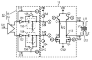
- FIG. 3 is a schematic circuit diagram of a primary circuit of the signal transmission circuit according to the embodiment.
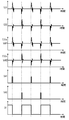
- FIG. 4 is a diagram illustrating a signal of the primary circuit of the signal transmission circuit according to the embodiment.
- FIG. 5 is a diagram illustrating a signal of the secondary circuit of the signal transmission circuit according to the embodiment.
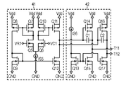
- FIG. 6A is a schematic block diagram of a feedback circuit of the signal transmission circuit according to the embodiment.
- FIG. 6B is a schematic circuit diagram of a differential amplifier circuit and a control circuit of the signal transmission circuit according to the embodiment.
- FIG. 7 is a schematic circuit diagram of a secondary circuit of the signal transmission circuit of the comparative example.
- FIG. 8 is a waveform diagram showing the result of simulation of the operation of the signal transmission circuit of the comparative example.
- FIG. 9 is a waveform diagram showing the result of simulation of the operation of the signal transmission circuit according to the embodiment.
- FIG. 10 is a diagram illustrating frequency characteristics of the feedback circuit of the signal transmission circuit according to the embodiment.
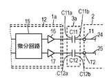
- FIG. 11 is a schematic circuit diagram of another primary circuit and another insulating circuit of the signal transmission circuit according to the embodiment.
- the signal transmission circuit 100 includes an insulating circuit 3 having a transformer including a primary coil L1 that is a primary element and a secondary coil L2 that is a secondary element, a secondary circuit 2, and a feedback circuit 4. Differential signals S21 and S22 generated from the transmission signal S1 are input to the primary coil L1.
- the secondary coil L2 is magnetically coupled to the primary coil L1, and outputs AC signals S31 and S32 including AC components of the differential signals S21 and S22.
- the secondary circuit 2 is electrically connected to the secondary coil L2, and has a pair of transmission lines 24 and 25 through which alternating current signals S31 and S32 flow. Further, the secondary circuit 2 extracts the transmission signal S1 from the AC signals S31 and S32 and outputs it as the output signal S5.
- the signal transmission circuit 100 of the present embodiment will be described in detail.
- the configuration described below is only an example of the present invention, and the present invention is not limited to the following embodiment, and the technical idea according to the present invention is not deviated from this embodiment.
- Various changes can be made in accordance with the design or the like as long as they are not.
- the primary circuit 1 is electrically connected to the primary coil L1 (primary element), and generates differential signals S21 and S22 from the transmission signal S1.
- the transmission signal S1 is a signal that electrically indicates data.
- the data is serial data.
- the primary circuit 1 includes a waveform shaping circuit 11, an AC component extraction circuit 12, and a drive circuit 13.
- the waveform shaping circuit 11 is composed of, for example, a Schmitt trigger circuit.
- the waveform shaping circuit 11 amplifies the harmonic component of the transmission signal S1 by sharply shaping the rising edge and the falling edge of the transmission signal S1.
- the waveform shaping circuit 11 is not limited to the Schmitt trigger circuit, and the waveform shaping circuit 11 may have another configuration.
- Switching elements 155 and 156 are electrically connected in parallel to differentiators 153 and 154, respectively. Switching elements 155 and 156 are switched on / off by differential signals S12 and S13, respectively. In the embodiment, the switching element 155 is turned on when the differential signal S12 is at a high level, and is turned off when the differential signal S12 is at a low level. The switching element 156 is turned on when the differential signal S13 is at a high level, and is turned off when the differential signal S13 is at a low level.
- the signals output from the NOT elements 151 and 152 do not pass through the differentiators 153 and 154 when the differential signals S12 and S13 are at a high level, respectively, and pass through the differentiators 153 and 154 when at a low level. . Therefore, the differential signal S14 is a signal obtained by differentiating the rising edge of the signal S11 as shown in FIG. Further, as shown in FIG. 4, the differential signal S15 is a signal obtained by differentiating the falling edge of the signal S11.
- the differential signal S14 is offset by a constant current source IS3 that supplies a constant current to the power supply potential point Vdd.
- the differential signal S15 is offset by a constant current source IS4 that supplies a constant current to the circuit ground GND.
- the drive circuit 13 is a differential signal S21, which is a current signal for driving the primary coil L1 of the insulation circuit 3, based on the differential signals S12 to S15 output from the differentiation circuit 15. S22 is generated and output.
- the drive circuit 13 is composed of four switching elements Q1 to Q4.
- the switching elements Q1, Q2 are npn-type bipolar transistors.
- the switching elements Q3 and Q4 are enhancement-type n-channel MOSFETs (Metal-Oxide-Semiconductor Field-Effect Transistors).
- the collectors of the switching elements Q1 and Q2 are electrically connected to the power supply potential point Vdd.
- a differential signal S14 is input to the base of the switching element Q1 (point a in FIG. 3). Further, the differential signal S15 is input to the base of the switching element Q2 (point b in FIG. 3).
- the sources of the switching elements Q3 and Q4 are electrically connected to the circuit ground GND.
- the differential signal S12 is input to the gate of the switching element Q3 (point c in FIG. 3). Further, the differential signal S13 is input to the gate of the switching element Q4 (point d in FIG. 3).
- the secondary circuit 2 includes an A / D conversion circuit 21 and an extraction circuit 22. Further, the secondary circuit 2 has a pair of transmission lines 24 and 25 through which the AC signals S31 and S32 flow, respectively.
- the comparators 211 and 212 are electrically connected to the pair of transmission lines 24 and 25, respectively.
- the comparators 211 and 212 compare the AC signals S31 and S32 input from the pair of transmission lines 24 and 25.
- the AC signal S31 is input to the inverting input terminal 211a of the comparator 211.
- a signal S32a obtained by superimposing the offset voltage Voff1 on the AC signal S32 is input to the non-inverting input terminal 211b of the comparator 211.
- the offset voltage Voff1 (see FIG. 5) is generated by the resistor R3 and the constant current source IS1.
- the resistor R3 is electrically connected between the non-inverting input terminal 211b of the comparator 211 and the transmission line 25.
- the constant current source IS1 is electrically connected between a connection point P101 where one end of the resistor R3 and the non-inverting input terminal 211b of the comparator 211 are connected, and the power supply potential point Vdd.
- the comparator 211 outputs a pulse signal S41 that is at a high level when the signal S32a is greater than the AC signal S31 and that is at a low level when the signal S32a is equal to or less than the AC signal S31.
- the pulse signal S41 is made up of pulses generated at substantially the same timing as the transmission signal S1 falls. That is, the comparator 211 outputs a signal (pulse signal S41) corresponding to the falling edge of the transmission signal S1.
- the AC signal S32 is input to the inverting input terminal 212a of the comparator 212.
- a signal S31a obtained by superimposing the offset voltage Voff2 on the AC signal S31 is input to the non-inverting input terminal 212b of the comparator 212.
- the offset voltage Voff2 is generated by the resistor R4 and the constant current source IS2.
- the resistor R4 is electrically connected between the non-inverting input terminal 212b of the comparator 212 and the transmission line 24.
- the constant current source IS2 is electrically connected between a connection point P102 where one end of the resistor R4 and the non-inverting input terminal 212b of the comparator 212 are connected, and the power supply potential point Vdd.
- the comparator 212 outputs a pulse signal S42 that is at a high level when the signal S31a is greater than the AC signal S32 and that is at a low level when the signal S31a is equal to or less than the AC signal S32.
- the pulse signal S42 is composed of pulses that are generated at substantially the same timing as the transmission signal S1 rises. That is, the comparator 212 outputs a signal (pulse signal S42) corresponding to the rising edge of the transmission signal S1.
- the offset voltages Voff1 and Voff2 are applied to the non-inverting input terminals 211b and 212b of the comparator 211 and the comparator 212, respectively. For this reason, in the signal transmission circuit 100 of this embodiment, chattering in the comparator 211 and the comparator 212 can be prevented.
- the signal transmission circuit 100 of this embodiment includes a trimming circuit that can arbitrarily adjust the offset voltages Voff1 and Voff2.
- the trimming circuit arbitrarily adjusts the offset voltages Voff1 and Voff2, for example, by adjusting the current value of the current flowing through the constant current sources IS1 and IS2.
- a trimming circuit it is optional whether or not a trimming circuit is provided, and further whether or not a configuration for applying the offset voltages Voff1 and Voff2 to the comparator 211 and the comparator 212 is provided.
- extracting the transmission signal S1 means extracting the transmission signal S1 in such a manner that data transmitted from the primary circuit 1 to the secondary circuit 2 can be extracted. That is, the transmission signal S1 extracted by the extraction circuit 22 only needs to have the same signal information as the transmission signal S1 input to the primary circuit 1, and the waveform shape such as the amplitude of the transmission signal S1 is the same. There may be no delay, and the transmission signal S1 input to the primary circuit 1 may be delayed.
- the pulse signal S41 is input to the reset terminal 22b of the extraction circuit 22, and the pulse signal S42 is input to the set terminal 22a.
- the extraction circuit 22 outputs an output signal S5 that goes high when the pulse of the pulse signal S42 is input to the set terminal 22a and goes low when the pulse of the pulse signal S41 is input to the reset terminal 22b.
- the timing at which the pulse of the pulse signal S41 is generated is almost the same as the timing at which the transmission signal S1 falls.
- the timing at which the pulse of the pulse signal S42 is generated is almost the same as the timing at which the transmission signal S1 rises.
- the output signal S5 is a signal that alternately becomes a low level and becomes a high level at almost the same timing as the rising and falling edges of the transmission signal S1. That is, the extraction circuit 22 extracts the transmission signal S1 and outputs it as the output signal S5.
- FIG. 6A is a schematic block diagram of the feedback circuit 4.
- the feedback circuit 4 includes a differential amplifier circuit 41 and a control circuit 42 as shown in FIG. 6A.
- the control circuit 42 includes a buffer 421 and a buffer 422.
- the control circuit 42 has a pair of terminals T11 and T12. As shown in FIG. 2, the pair of terminals T11 and T12 are electrically connected to nodes 26 and 27, respectively.
- the nodes 26 and 27 are provided in the pair of transmission lines 24 and 25, respectively, as shown in FIG.
- the terminals T11 and T12 may be part of a conductor formed as a wiring on a substrate, for example.
- the drain of the switching element Q5 is electrically connected to the drain and gate of the switching element Q7.
- the gate of the switching element Q7 is electrically connected to the gate of the switching element Q8.
- the drain of switching element Q8 is electrically connected to the drain and gate of switching element Q9.
- the sources of the switching elements Q7 and Q8 are electrically connected to the power supply potential point Vdd.
- the source of the switching element Q9 is electrically connected to the circuit ground GND. That is, the switching elements Q5, Q7 to Q9 constitute a current mirror circuit.
- the drain of the switching element Q6 is electrically connected to the drain and gate of the switching element Q10.
- the gate of the switching element Q10 is electrically connected to the gate of the switching element Q11.
- the drain of the switching element Q11 is electrically connected to the drain of the switching element Q12.
- the gate of the switching element Q12 is electrically connected to the gate of the switching element Q9.
- the sources of the switching elements Q10 and Q11 are electrically connected to the power supply potential point Vdd.
- the source of the switching element Q12 is electrically connected to the circuit ground GND. That is, the switching elements Q6, Q10 to Q12 constitute a current mirror circuit.
- the differential amplifier circuit 41 outputs a current signal that increases or decreases according to the difference between the intermediate voltage VC1 and the reference voltage VR1 to the buffer 421 and the buffer 422. That is, the differential amplifier circuit 41 increases the output current signal when the intermediate voltage VC1 exceeds the reference voltage VR1. Further, the differential amplifier circuit 41 reduces the output current signal when the intermediate voltage VC1 falls below the reference voltage VR1.
- the buffer 422 is a current mirror circuit including three switching elements Q13, Q16, and Q17, a capacitor C2, and a constant current source IS6 shown in FIG. 6B.
- the switching element Q16 is an enhancement type p-channel MOSFET.
- the switching element Q17 is an enhancement type n-channel MOSFET. That is, the buffer 421 and the buffer 422 share the switching element Q13 and the constant current source IS6.
- the gate of the switching element Q17 is electrically connected to the gate of the switching element Q13.
- the drain of the switching element Q17 is electrically connected to the drain of the switching element Q16.
- a capacitor C2 is electrically connected between the gate and drain of the switching element Q16.
- the source of the switching element Q16 is electrically connected to the power supply potential point Vdd.
- the source of the switching element Q17 is electrically connected to the circuit ground GND.
- the control circuit 42 controls the current flowing through the nodes 26 and 27 according to the signal output from the differential amplifier circuit 41. That is, when the intermediate voltage VC1 exceeds the reference voltage VR1, the drain current of the switching elements Q14 and Q16 becomes larger than the current flowing through the constant current source IS6, so that the control circuit 42 goes from the terminals T11 and T12 to the nodes 26 and 27. And operate to pass current. Further, when the intermediate voltage VC1 falls below the reference voltage VR1, the drain current of the switching elements Q14 and Q16 becomes smaller than the current flowing through the constant current source IS6, so that the control circuit 42 goes from the nodes 26 and 27 to the terminals T11 and T12. And operate to draw current.
- the feedback circuit 4 is electrically connected to the nodes 26 and 27 provided in the pair of transmission lines 24 and 25, respectively.
- the feedback circuit 4 feeds back the intermediate voltage VC1 by controlling the current flowing through the nodes 26 and 27 according to the difference between the intermediate voltage VC1 and the reference voltage VR1.
- the nodes 26 and 27 are preferably connected directly to the input terminals T1 and T2 of the secondary circuit 2, respectively.
- the nodes 26 and 27 are preferably directly connected to both ends of the secondary coil L2 that generates the AC signals S31 and S32. That is, the nodes 26 and 27 have the input terminals T1 and T2 (or the secondary coil L2) so that no wiring impedance is interposed between the nodes 26 and 27 and the input terminals T1 and T2 (or both ends of the secondary coil L2). Are preferably connected to both ends).
- the intermediate voltage VC1 can be fed back by the feedback circuit 4 so as to avoid the influence of the wiring impedance of the pair of transmission lines 24 and 25 as much as possible.
- the primary circuit 1 generates differential signals S21 and S22 from the transmission signal S1 and outputs them to the primary coil L1.
- the differential signals S21 and S22 are input to the primary coil L1, an alternating current flows through the primary coil L1.
- AC signals S31 and S32 including AC components of the differential signals S21 and S22 are generated when an AC current flows through the primary coil L1.
- the comparator 211 compares the AC signals S31 and S32 and outputs a pulse signal S41 corresponding to the falling edge of the transmission signal S1.
- the comparator 212 compares the AC signals S31 and S32 and outputs a pulse signal S42 corresponding to the rising edge of the transmission signal S1.
- the extraction circuit 22 extracts the transmission signal S1 based on the pulse signals S41 and S42 and outputs it as the output signal S5.
- the primary circuit 1 generates differential signals S21 and S22 from the input transmission signal S1 and transmits them to the secondary circuit 2 via the insulation circuit 3. Then, the secondary circuit 2 extracts the transmission signal S1 from the signal transmitted from the primary circuit 1, thereby outputting an output signal S5 corresponding to the transmission signal S1.
- parasitic capacitances Cp1 and Cp2 exist between the primary coil L1 (primary element) and the secondary coil L2 (secondary element) as shown in FIG.
- the noise may be transmitted to the secondary circuit 2 via the parasitic capacitances Cp1 and Cp2.
- FIG. 7 is a schematic circuit diagram of the secondary circuit 200 of the signal transmission circuit of the comparative example.
- the same reference numerals are assigned to the same parts as those of the secondary circuit 2 shown in FIG.
- the signal transmission circuit (secondary circuit 200) of the comparative example has the same configuration as the signal transmission circuit 100 (secondary circuit 2) of the present embodiment, except that the feedback circuit 4 is not provided.
- FIG. 8 shows a signal obtained by a simulation in which common mode noise is applied to the primary circuit of the signal transmission circuit of the comparative example.
- the vertical axis represents the signal value
- the horizontal axis represents time.
- a positive voltage CN1 of several tens of kV simulating common mode noise is applied to the primary circuit from time t0 to time t3.
- time t0 and time t1 for example, 1 ⁇ s
- the voltage level of the AC signals S31 and S32 is relatively lowered due to the increase of the intermediate voltage VC1.
- the voltage levels of the AC signals S31 and S32 are out of the allowable input voltage range of the comparator 211 and the comparator 212, so that the comparator 211 and the comparator 212 malfunction.
- FIG. 9 shows the result of a simulation in which common mode noise is applied to the primary circuit 1 of the signal transmission circuit 100 of this embodiment.
- the vertical axis indicates signal Ata
- the horizontal axis indicates time.
- the feedback circuit 4 causes the intermediate voltage VC1 to converge to the reference voltage VR1. Since the intermediate voltage VC1 is fed back, the intermediate voltage VC1 hardly fluctuates. Even when the negative voltage CN1 is applied, the intermediate voltage VC1 hardly fluctuates for the same reason. For this reason, since the voltage levels of the AC signals S31 and S32 hardly fluctuate, the AC signals S31 and S32 hardly fall outside the allowable input voltage range of the comparator 211 and the comparator 212, and the comparator 211 and the comparator 212 are unlikely to malfunction.
- the pulse signals S41 and S42 input to the extraction circuit 22 are not likely to be abnormal, and the output signal S5 is likely to be normally output from the extraction circuit 22. That is, a transmission error of the transmission signal S1 hardly occurs.
- the feedback circuit 4 causes the intermediate voltage VC1 to converge to the reference voltage VR1.
- the signal transmission circuit 100 of this embodiment fluctuations in the input voltage of the secondary circuit 2 (particularly, the input voltages to the comparator 211 and the comparator 212) can be suppressed. Therefore, the signal transmission circuit 100 according to the present embodiment hardly causes a malfunction of the secondary circuit 2 even when noise is applied to the primary circuit 1.
- the signal transmission circuit 100 of the present embodiment it is difficult to cause malfunction of the secondary circuit 2 by providing the feedback circuit 4 without providing two transformers. And increase in cost can be suppressed.
- the frequency of noise (common mode noise) assumed in the signal transmission circuit 100 of the present embodiment is several hundred MHz or less, depending on the frequency of occurrence.
- the frequencies of the AC signals S31 and S32 output from the secondary coil L2 (secondary element) are matched to the characteristics of the transformer (the primary coil L1 and the secondary coil L2). It is several hundred MHz or more or about several GHz.
- the feedback circuit 4 is preferably configured to limit the passage of the AC signals S31 and S32.
- FIG. 10 shows the frequency characteristics of the feedback circuit 4.
- the feedback circuit 4 is preferably configured such that the cutoff frequency fc1 is located between f0 and f1, that is, satisfies the relationship of f0 ⁇ fc1 ⁇ f1.
- the feedback circuit 4 responds to common mode noise having a frequency lower than the cutoff frequency fc1, and the feedback circuit 4 becomes difficult to respond to AC signals S31 and S32 having a frequency higher than the cutoff frequency fc1. .
- the cutoff frequency fc1 is determined by the capacitance component and the resistance component of the feedback circuit 4.
- the capacitance component and the resistance component can be appropriately changed by adjusting the size of the switching elements Q5 to Q17 included in the feedback circuit 4 and the current flowing through the constant current source IS3, for example.
- the insulating circuit 3 includes a primary coil L1 (primary element) and a secondary coil L2 (secondary element) that are magnetically coupled to each other. That is, in the signal transmission circuit 100 of the present embodiment, the primary element and the secondary element are magnetically coupled to each other, but may have other configurations.
- the electrodes C11a and C12a of the capacitors C11 and C12 are electrically connected to the output terminals of the buffers 16 and 17 of the primary circuit 1a, respectively.
- the electrodes C11b and C12b of the capacitors C11 and C12 are connected to the input terminals T1 and T2 of the secondary circuit 2, respectively.
- the electrodes C11a and C12a on the primary circuit 1 side of the capacitors C11 and C12 function as primary elements
- the electrodes C11b and C12b on the secondary circuit 2 side of the capacitors C11 and C12 function as secondary elements. That is, in the signal transmission circuit 100 of this embodiment, the primary element and the secondary element may be capacitively coupled to each other.
Landscapes
- Engineering & Computer Science (AREA)
- Computer Hardware Design (AREA)
- Physics & Mathematics (AREA)
- Power Engineering (AREA)
- Signal Processing (AREA)
- Computer Networks & Wireless Communication (AREA)
- Computing Systems (AREA)
- Nonlinear Science (AREA)
- Mathematical Physics (AREA)
- General Engineering & Computer Science (AREA)
- Dc Digital Transmission (AREA)
- Electronic Switches (AREA)
- Logic Circuits (AREA)
- Near-Field Transmission Systems (AREA)
Abstract
信号伝送回路は、伝送信号から生成されて交流成分を有する差動信号が入力される一次素子と、一次素子と磁気結合または容量結合して差動信号の交流成分を含む交流信号を出力する二次素子と、二次素子と電気的に接続されてかつ交流信号が流れる一対の伝送線路を有して交流信号から伝送信号を抽出する二次回路と、一対の伝送線路間の電圧の中間電圧を基準電圧に収束させるように中間電圧を帰還する帰還回路とを備える。この信号伝送回路は、ノイズが印加されても、二次回路の誤動作を引き起こし難い。
Description
本発明は、一般に信号伝送回路、より詳細には、一次回路と二次回路とが磁気結合または容量結合した信号伝送回路に関する。
磁気結合を用いて一次回路から二次回路に信号を伝送する無線通信システム(信号伝送回路)が知られており、たとえば特許文献1に開示されている。この無線通信システムは、送信機と、受信機とを備えている。
送信機は、送信データが入力される送信回路(一次回路)と、送信アンテナとしての送信コイルとを備えている。送信回路は、送信データに対応した電流を送信コイルに流すことで、送信コイルに送信データに対応した磁界変化を発生させる。
受信機は、受信アンテナとしての受信コイルと、受信回路(二次回路)とを備えている。受信コイルは、送信コイルと誘導結合され、送信コイルで発生する磁界変化を検出する。受信回路は、受信コイルの一端および他端に発生する誘導起電力に基づいて、受信データを生成する。
信号伝送回路は、伝送信号から生成されて交流成分を有する差動信号が入力される一次素子と、一次素子と磁気結合または容量結合して差動信号の交流成分を含む交流信号を出力する二次素子と、二次素子と電気的に接続されてかつ交流信号が流れる一対の伝送線路を有して交流信号から伝送信号を抽出する二次回路と、一対の伝送線路の電圧の間の電圧の中間電圧を基準電圧に収束させるように中間電圧を帰還する帰還回路とを備える。
この信号伝送回路は、ノイズが印加されても、二次回路の誤動作を引き起こし難い。
図1と図2はそれぞれ実施形態に係る信号伝送回路100の概略ブロック図と概略回路図である。信号伝送回路100は、一次素子である一次コイルL1および二次素子である二次コイルL2からなるトランスを有する絶縁回路3と、二次回路2と、帰還回路4とを備えている。一次コイルL1には、伝送信号S1から生成される差動信号S21、S22が入力される。
二次コイルL2は、一次コイルL1と磁気結合し、差動信号S21、S22の交流成分を含む交流信号S31、S32を出力する。二次回路2は、二次コイルL2と電気的に接続され、交流信号S31、S32が流れる一対の伝送線路24、25を有している。また、二次回路2は、交流信号S31、S32から伝送信号S1を抽出し、出力信号S5として出力する。
帰還回路4は、一対の伝送線路24、25の電圧の間の中間電圧VC1を基準電圧VR1に収束させるように中間電圧VC1を帰還する。
以下、本実施形態の信号伝送回路100について詳細に説明する。ただし、以下に説明する構成は、本発明の一例に過ぎず、本発明は下記の実施形態に限定されることはなく、この実施形態以外であっても、本発明に係る技術的思想を逸脱しない範囲であれば、設計等に応じて種々の変更が可能である。
一次回路1は、一次コイルL1(一次素子)と電気的に接続され、伝送信号S1から差動信号S21、S22を生成する。伝送信号S1はデータを電気的に示す信号である。本実施形態ではデータはシリアルデータである。一次回路1は、波形整形回路11と、交流成分抽出回路12と、駆動回路13とを備えている。
波形整形回路11は、たとえばシュミットトリガ回路で構成されている。波形整形回路11は、伝送信号S1の立ち上がりエッジおよび立ち下がりエッジを急峻に整形することで、伝送信号S1の高調波成分を増幅する。なお、波形整形回路11をシュミットトリガ回路に限定する趣旨ではなく、波形整形回路11は他の構成であってもよい。
交流成分抽出回路12は、信号変換回路14と、微分回路15とを備えている。信号変換回路14は差動アンプで構成されている。図3は一次回路1の概略回路図である。図4は一次回路1の動作波形図である。図5は二次回路2動作波形図である。図4と図5において、縦軸は信号の値を示し、横軸は時間を示す。信号変換回路14は、図3に示すように、波形整形回路11から出力されるシングルエンドの信号S11を2つの差動信号S12、S13に変換して出力する。差動信号S13は、図4に示すように、信号S11から僅かに位相が遅れている。また、差動信号S12は、図4に示すように、差動信号S13の位相を反転した信号である。
微分回路15は、図3に示すように、信号変換回路14から出力される差動信号S12、S13を微分することで、差動信号S12、S13の交流成分を抽出した差動信号S14、S15を出力する。微分回路15は、2つのNOT素子151、152と、2つの微分器153、154と、2つのスイッチング素子155、156とを備えている。NOT素子151、152は、それぞれ差動信号S12、S13の位相を反転した信号を出力する。微分器153、154は、それぞれNOT素子151、152から出力される信号を微分して出力する。微分器153、154は、たとえば抵抗およびキャパシタを有するRC回路で構成される。
スイッチング素子155、156は、それぞれ微分器153、154に並列に電気的に接続される。スイッチング素子155、156は、それぞれ差動信号S12、S13によりオン/オフが切り替えられる。実施形態では、スイッチング素子155は差動信号S12がハイレベルのときにオンに切り替わり、ローレベルのときにオフに切り替わる。スイッチング素子156は、差動信号S13がハイレベルのときにオンに切り替わり、ローレベルのときにオフに切り替わる。
したがって、NOT素子151、152から出力される信号は、それぞれ差動信号S12、S13がハイレベルのときは微分器153、154を通過せず、ローレベルのときに微分器153、154を通過する。このため、差動信号S14は、図4に示すように、信号S11の立ち上がりエッジを微分した信号となる。また、差動信号S15は、図4に示すように、信号S11の立ち下がりエッジを微分した信号となる。なお、差動信号S14は、電源電位点Vddに一定電流を流す定電流源IS3により、オフセットが与えられている。また、差動信号S15は、回路グランドGNDに一定電流を流す定電流源IS4により、オフセットが与えられている。
駆動回路13は、図3に示すように、微分回路15から出力される差動信号S12~S15に基づいて、絶縁回路3の一次コイルL1を駆動するための電流信号である差動信号S21、S22を生成して出力する。駆動回路13は、4つのスイッチング素子Q1~Q4で構成されている。スイッチング素子Q1、Q2は、npn型のバイポーラトランジスタである。スイッチング素子Q3、Q4は、エンハンスメント型のnチャネルMOSFET(Metal-Oxide-Semiconductor Field-Effect Transistor)である。
スイッチング素子Q1、Q2のコレクタは電源電位点Vddに電気的に接続されている。スイッチング素子Q1のベースには差動信号S14が入力される(図3の点a)。また、スイッチング素子Q2のベースには差動信号S15が入力される(図3の点b)。スイッチング素子Q3、Q4のソースは回路グランドGNDに電気的に接続されている。スイッチング素子Q3のゲートには差動信号S12が入力される(図3の点c)。また、スイッチング素子Q4のゲートには差動信号S13が入力される(図3の点d)。スイッチング素子Q1のエミッタおよびスイッチング素子Q3のドレインが接続されている接続点N12は、一次コイルL1の端L11に電気的に接続されている。また、スイッチング素子Q2のエミッタおよびスイッチング素子Q4のドレインが接続されている接続点N13は一次コイルL1の端L12に電気的に接続されている。
図4は一次回路1の信号を示す。駆動回路13により、電流である差動信号S21が一次コイルL1の端L11に入力される。また、駆動回路13により、電流である差動信号S22が一次コイルL1の端L12に入力される。差動信号S22は、差動信号S21の位相を反転した信号である。したがって、一次コイルL1には、図4に示す交流電圧V1が印加される。
言い換えれば、駆動回路13は、微分された差動信号S21、S22のうち伝送信号S1の立ち上がりに対応する信号である差動信号S21を一次コイルL1の端L11に出力する。また、駆動回路13は、微分された差動信号S21、S22のうち伝送信号S1の立ち下がりに対応する信号である差動信号S22を一次コイルL1の端L12に出力する。
ところで、単にデータに応じた矩形波を一次コイルL1および二次コイルL2よりなるトランスに入力する場合でも、一次コイルL1に入力される信号の交流成分が二次コイルL2に伝わる。しかしながら、トランスは直流成分に対してはインピーダンスが低いため、単にデータに応じた矩形波をトランスに入力した場合、一次コイルL1および一次回路1に電流が流れ続け、消費電力が増大するおそれがある。
本実施形態の信号伝送回路100では、一次回路1の微分回路15により、一次コイルL1に入力される信号の直流成分を除いている。したがって、本実施形態の信号伝送回路100では、一次コイルL1および一次回路1に電流が流れ続けることがなく、消費電力の低減を図ることができる。なお、一次回路1は微分回路15を備えていなくてもよい。
二次回路2は、図1、図2に示すように、A/D変換回路21と、抽出回路22とを備えている。また、二次回路2は、交流信号S31、S32がそれぞれ流れる一対の伝送線路24、25を有している。
A/D変換回路21は、二次コイルL2から出力されるアナログ信号である交流信号S31、S32をディジタルのパルス信号S41、S42に変換して出力する。A/D変換回路21は、コンパレータ211、212と分圧回路23とを備えている。
コンパレータ211、212は、一対の伝送線路24、25にそれぞれ電気的に接続されている。コンパレータ211、212は、一対の伝送線路24、25から入力される交流信号S31、S32を比較する。
コンパレータ211の反転入力端子211aには、交流信号S31が入力される。コンパレータ211の非反転入力端子211bには、オフセット電圧Voff1を交流信号S32に重畳して得られる信号S32aが入力される。オフセット電圧Voff1(図5参照)は抵抗R3および定電流源IS1により生成される。抵抗R3は、コンパレータ211の非反転入力端子211bと伝送線路25との間に電気的に接続される。定電流源IS1は、抵抗R3の一端とコンパレータ211の非反転入力端子211bとが接続された接続点P101と電源電位点Vddとの間に電気的に接続される。
コンパレータ211は、信号S32aが交流信号S31よりも大きいときにハイレベルとなり、信号S32aが交流信号S31以下であるときにローレベルとなるパルス信号S41を出力する。パルス信号S41は、伝送信号S1が立ち下がるタイミングとほぼ同じタイミングで発生するパルスよりなる。つまり、コンパレータ211は、伝送信号S1の立ち下がりに対応する信号(パルス信号S41)を出力する。
コンパレータ212の反転入力端子212aには交流信号S32が入力される。コンパレータ212の非反転入力端子212bには、オフセット電圧Voff2を交流信号S31に重畳して得られた信号S31aが入力される。オフセット電圧Voff2は、抵抗R4および定電流源IS2により生成される。抵抗R4は、コンパレータ212の非反転入力端子212bと伝送線路24との間に電気的に接続される。定電流源IS2は、抵抗R4の一端とコンパレータ212の非反転入力端子212bとが接続された接続点P102と電源電位点Vddとの間に電気的に接続される。
コンパレータ212は、信号S31aが交流信号S32よりも大きいときにハイレベルとなり、信号S31aが交流信号S32以下であるときにローレベルとなるパルス信号S42を出力する。パルス信号S42は、伝送信号S1が立ち上がるタイミングとほぼ同じタイミングで発生するパルスよりなる。つまり、コンパレータ212は、伝送信号S1の立ち上がりに対応する信号(パルス信号S42)を出力する。
上述のように、本実施形態の信号伝送回路100では、コンパレータ211およびコンパレータ212の非反転入力端子211b、212bにオフセット電圧Voff1、Voff2をそれぞれ与えている。このため、本実施形態の信号伝送回路100では、コンパレータ211およびコンパレータ212でのチャタリングを防止することができる。
なお、本実施形態の信号伝送回路100は、オフセット電圧Voff1、Voff2を任意に調整することのできるトリミング回路を備えていることが好ましい。この構成では、部品のばらつきなどによりコンパレータ211およびコンパレータ212の感度が変動した場合に、トリミング回路により感度を調整することができる。トリミング回路は、たとえば定電流源IS1、IS2の流す電流の電流値を調整することで、オフセット電圧Voff1、Voff2を任意に調整する。もちろん、トリミング回路を備えるか否か、さらにはコンパレータ211およびコンパレータ212にオフセット電圧Voff1、Voff2を与える構成を備えるか否かは任意である。
分圧回路23は、一対の伝送線路24、25間の電圧を分圧するように構成されている。分圧回路23は、互いに直列に接続された抵抗R1、R2よりなる直列回路で構成されている。抵抗R1の第1端は伝送線路24に電気的に接続されている。抵抗R2の第1端は、伝送線路25に電気的に接続されている。そして、抵抗R1の第2端と抵抗R2の第2端とが接続されている接続点P103には、一対の伝送線路24、25の電圧の間の中間電圧VC1が発生する。言い換えれば、中間電圧VC1は、分圧回路23により分圧された電圧である。
ここで、中間電圧VC1は、一対の伝送線路24、25間の電圧を分圧した電圧であればよく、抵抗R1、R2の抵抗値は等しくなくてもよい。なお、抵抗R1、R2の抵抗値を同じとすることにより、回路設計を簡素にできる。また、分圧回路23は、2つの抵抗R1、R2の直列回路のみならず、互いに直列に接続された3つ以上の抵抗よりなる直列回路で構成されていてもよい。また、分圧回路23は、抵抗の代わりに、互いに直列に接続された複数のキャパシタよりなる直列回路で構成されていてもよい。なお、本実施形態の信号伝送回路100が分圧回路23を備えるか否かは任意である。
抽出回路22は、たとえばRSフリップフロップ回路で構成されている。抽出回路22は、パルス信号S41、S42に基づいて伝送信号S1を抽出し、出力信号S5として出力する。言い換えれば、抽出回路22は、コンパレータ(コンパレータ211およびコンパレータ212)の比較結果に基づいて伝送信号S1を抽出する。
ここで、「伝送信号S1を抽出する」とは、一次回路1から二次回路2に伝送されるデータを取り出すことのできる形で伝送信号S1を抽出することを意味する。つまり、抽出回路22で抽出される伝送信号S1は、一次回路1に入力される伝送信号S1と同一の信号情報を有していればよく、伝送信号S1の振幅などの波形の形状は同一でなくてもよく、一次回路1に入力される伝送信号S1から遅延していてもよい。
具体的には、抽出回路22のリセット端子22bにパルス信号S41が入力され、セット端子22aにパルス信号S42が入力される。抽出回路22は、セット端子22aにパルス信号S42のパルスが入力されるとハイレベルになり、リセット端子22bにパルス信号S41のパルスが入力されるとローレベルとなる出力信号S5を出力する。既に述べたように、パルス信号S41のパルスが発生するタイミングは、伝送信号S1が立ち下がるタイミングとほぼ同じである。また、パルス信号S42のパルスが発生するタイミングは、伝送信号S1が立ち上がるタイミングとほぼ同じである。したがって、出力信号S5は、伝送信号S1の立ち上がりと立ち下がりとそれぞれほぼ同じタイミングで交互にローレベルとなりハイレベルとなる信号となる。つまり、抽出回路22は、伝送信号S1を抽出し、出力信号S5として出力する。
図6Aは帰還回路4の概略ブロック図である。帰還回路4は、図6Aに示すように、差動増幅回路41と、制御回路42とを備えている。制御回路42は、バッファ421と、バッファ422とを備えている。また、制御回路42は、一対の端子T11、T12を有している。図2に示すように、一対の端子T11、T12は、それぞれノード26、27に電気的に接続されている。ここで、ノード26、27は、図2に示すように、一対の伝送線路24、25にそれぞれ設けられている。なお、端子T11、T12は、たとえば基板上に配線として形成された導体の一部であってもよい。
図6Bは差動増幅回路41と制御回路42の概略回路図である。差動増幅回路41は、図6Bに示すように、8つのスイッチング素子Q5~Q12と、定電流源IS5とを備えている。スイッチング素子Q5、Q6、Q9、Q12は、エンハンスメント型のnチャネルMOSFETである。スイッチング素子Q7、Q8、Q10、Q11は、エンハンスメント型のpチャネルMOSFETである。スイッチング素子Q5のゲートには基準電圧VR1が入力される。ここで、基準電圧VR1は、たとえばBGR(Band Gap Reference)回路で生成される電圧である。スイッチング素子Q6のゲートには中間電圧VC1が入力される。スイッチング素子Q5、Q6のソースは定電流源IS5に電気的に接続されている。定電流源IS5は回路グランドGNDに一定電流を流す。
スイッチング素子Q5のドレインは、スイッチング素子Q7のドレインおよびゲートに電気的に接続されている。スイッチング素子Q7のゲートは、スイッチング素子Q8のゲートに電気的に接続されている。スイッチング素子Q8のドレインは、スイッチング素子Q9のドレインおよびゲートに電気的に接続されている。スイッチング素子Q7、Q8のソースは、電源電位点Vddに電気的に接続されている。スイッチング素子Q9のソースは、回路グランドGNDに電気的に接続されている。つまり、スイッチング素子Q5、Q7~Q9は、カレントミラー回路を構成している。
スイッチング素子Q6のドレインは、スイッチング素子Q10のドレインおよびゲートに電気的に接続されている。スイッチング素子Q10のゲートは、スイッチング素子Q11のゲートに電気的に接続されている。スイッチング素子Q11のドレインは、スイッチング素子Q12のドレインに電気的に接続されている。スイッチング素子Q12のゲートは、スイッチング素子Q9のゲートに電気的に接続されている。スイッチング素子Q10、Q11のソースは、電源電位点Vddに電気的に接続されている。スイッチング素子Q12のソースは、回路グランドGNDに電気的に接続されている。つまり、スイッチング素子Q6、Q10~Q12は、カレントミラー回路を構成している。
差動増幅回路41は、中間電圧VC1と基準電圧VR1との差分に応じて増減する電流信号を、バッファ421およびバッファ422に出力する。つまり、差動増幅回路41は、中間電圧VC1が基準電圧VR1を上回ると、出力する電流信号を大きくする。また、差動増幅回路41は、中間電圧VC1が基準電圧VR1を下回ると、出力する電流信号を小さくする。
バッファ421は、図6Bに示す3つのスイッチング素子Q13~Q15と、キャパシタC1と、定電流源IS6とで構成されるカレントミラー回路である。スイッチング素子Q13、Q15は、エンハンスメント型のnチャネルMOSFETである。また、スイッチング素子Q14は、エンハンスメント型のpチャネルMOSFETである。定電流源IS6は、電源電位点Vddからスイッチング素子Q13のドレインへと一定電流を流す。スイッチング素子Q13のドレインおよびゲートは、電気的に接続されている。スイッチング素子Q13のゲートは、スイッチング素子Q15のゲートに電気的に接続されている。スイッチング素子Q15のドレインは、スイッチング素子Q14のドレインに電気的に接続されている。スイッチング素子Q14のゲート-ドレイン間には、キャパシタC1が電気的に接続されている。スイッチング素子Q14のソースは、電源電位点Vddに電気的に接続されている。スイッチング素子Q13、Q15のソースは、回路グランドGNDに電気的に接続されている。
バッファ422は、図6Bに示す3つのスイッチング素子Q13、Q16、Q17と、キャパシタC2と、定電流源IS6とで構成されるカレントミラー回路である。スイッチング素子Q16は、エンハンスメント型のpチャネルMOSFETである。また、スイッチング素子Q17は、エンハンスメント型のnチャネルMOSFETである。つまり、バッファ421およびバッファ422は、スイッチング素子Q13と、定電流源IS6とを共用している。スイッチング素子Q17のゲートは、スイッチング素子Q13のゲートに電気的に接続されている。スイッチング素子Q17のドレインは、スイッチング素子Q16のドレインに電気的に接続されている。スイッチング素子Q16のゲート-ドレイン間には、キャパシタC2が電気的に接続されている。スイッチング素子Q16のソースは、電源電位点Vddに電気的に接続されている。スイッチング素子Q17のソースは、回路グランドGNDに電気的に接続されている。
制御回路42は、差動増幅回路41から出力される信号に応じて、ノード26、27を流れる電流を制御する。つまり、中間電圧VC1が基準電圧VR1を上回ると、スイッチング素子Q14、Q16のドレイン電流が定電流源IS6の流す電流よりも大きくなるため、制御回路42は、端子T11、T12からノード26、27へと電流を流すように動作する。また、中間電圧VC1が基準電圧VR1を下回ると、スイッチング素子Q14、Q16のドレイン電流が定電流源IS6の流す電流よりも小さくなるため、制御回路42は、ノード26、27から端子T11、T12へと電流を引き込むように動作する。
このように、帰還回路4は、一対の伝送線路24、25にそれぞれ設けられたノード26、27に電気的に接続されている。そして、帰還回路4は、中間電圧VC1と基準電圧VR1との差分に応じて、ノード26、27を流れる電流を制御することで、中間電圧VC1を帰還する。
ここで、ノード26、27は、二次回路2の入力端T1、T2にそれぞれ直接的に接続されるのが好ましい。また、ノード26、27は、交流信号S31、S32を発生する二次コイルL2の両端にそれぞれ直接的に接続されるのが好ましい。つまり、ノード26、27は、ノード26、27と入力端T1、T2(または二次コイルL2の両端)との間に配線インピーダンスが介在しないように、入力端T1、T2(または二次コイルL2の両端)に接続されるのが好ましい。この構成では、一対の伝送線路24、25の配線インピーダンスの影響を極力避けるようにして、帰還回路4により中間電圧VC1を帰還させることができる。
以下、本実施形態の信号伝送回路100の動作について簡単に説明する。一次回路1は、伝送信号S1から差動信号S21、S22を生成し、一次コイルL1に出力する。差動信号S21、S22が一次コイルL1に入力されることで、一次コイルL1に交流電流が流れる。二次コイルL2には、一次コイルL1に交流電流が流れることで、差動信号S21、S22の交流成分を含む交流信号S31、S32が発生する。
二次回路2において、コンパレータ211は、交流信号S31、S32を比較して、伝送信号S1の立ち下がりに対応するパルス信号S41を出力する。また、コンパレータ212は、交流信号S31、S32を比較して、伝送信号S1の立ち上がりに対応するパルス信号S42を出力する。そして、抽出回路22は、パルス信号S41、S42に基づいて伝送信号S1を抽出し、出力信号S5として出力する。
つまり、本実施形態の信号伝送回路100では、一次回路1は、入力された伝送信号S1から差動信号S21、S22を生成し、絶縁回路3を介して二次回路2に伝送する。そして、二次回路2は、一次回路1から伝送された信号から伝送信号S1を抽出することで、伝送信号S1に相当する出力信号S5を出力する。
ところで、一次コイルL1(一次素子)と二次コイルL2(二次素子)との間には、図2に示すように、寄生容量Cp1、Cp2が存在する。たとえば雷サージなどにより、ノイズ特にコモンモードノイズが一次回路1に印加されると、寄生容量Cp1、Cp2を介してノイズが二次回路2に伝わることがある。
図7は、比較例の信号伝送回路の二次回路200の概略回路図である。図7において図2に示す二次回路2と同じ部分には同じ参照番号を付す。図7に示すように、比較例の信号伝送回路(二次回路200)は、帰還回路4を備えていないことを除いて、本実施形態の信号伝送回路100(二次回路2)と同じ構成を有する。以下、比較例の信号伝送回路の一次回路にノイズが印加された場合について説明する。図8は、比較例の信号伝送回路の一次回路にコモンモードノイズを印加したシミュレーションにより得られた信号を示す。図8において、縦軸は信号の値を示し、横軸は時間を示す。
図8に示すシミュレーションでは、比較例の信号伝送回路において、コモンモードノイズを模擬した数十kVの正極性の電圧CN1が、時刻t0から時刻t3まで一次回路に印加されている。時刻t0から時刻t1の間(たとえば1μs)においては、中間電圧VC1が上がることで、相対的に交流信号S31、S32の電圧レベルが下がる。このため、図8に示す例では、交流信号S31、S32の電圧レベルが、コンパレータ211およびコンパレータ212の許容される入力電圧の範囲から外れることで、コンパレータ211およびコンパレータ212が誤動作する。
同様に、時刻t2から時刻t3の間(たとえば1μs)においては、中間電圧VC1が下がることで、相対的に交流信号S31、S32の電圧レベルが上がる。このため、図8に示す例では、交流信号S31、S32の電圧レベルが、コンパレータ211およびコンパレータ212の許容される入力電圧の範囲から外れることで、コンパレータ211およびコンパレータ212が誤動作する。
したがって、比較例の信号伝送回路では、抽出回路22に入力されるパルス信号S41、S42に異常が生じるので、抽出回路22から出力信号S5が正常に出力されなくなる。つまり、伝送信号S1の伝送エラーが生じ易い。
前述の従来の信号伝送回路でも、たとえば雷サージなどにより一次回路にノイズが印加されると、ノイズが二次回路に伝わり、二次回路の誤動作を引き起こす可能性がある。
一方、本実施形態の信号伝送回路100の一次回路1にノイズが印加された場合について説明する。図9は、本実施形態の信号伝送回路100の一次回路1にコモンモードノイズを印加したシミュレーションの結果を示す。図9において、縦軸は信号の阿多を示し、横軸は時間を示す。
本実施形態の信号伝送回路100では、図9に示すように、コモンモードノイズを模擬した正極性の電圧CN1が印加されても、帰還回路4により中間電圧VC1が基準電圧VR1に収束するように中間電圧VC1が帰還されるので、中間電圧VC1は殆ど変動しない。なお、負極性の電圧CN1を印加した場合も、同様の理由で中間電圧VC1は殆ど変動しない。このため、交流信号S31、S32は、それらの電圧レベルも殆ど変動しないことから、コンパレータ211およびコンパレータ212の許容される入力電圧の範囲から外れ難く、コンパレータ211およびコンパレータ212が誤動作し難い。
このため、本実施形態の信号伝送回路100では、抽出回路22に入力されるパルス信号S41、S42にも異常が生じ難く、抽出回路22から出力信号S5が正常に出力され易い。つまり、伝送信号S1の伝送エラーが生じ難い。
上述のように、本実施形態の信号伝送回路100では、一次回路1にノイズが印加され、ノイズが二次回路2に伝わっても、帰還回路4により中間電圧VC1が基準電圧VR1に収束する。このため、本実施形態の信号伝送回路100では、二次回路2の入力電圧(とくに、コンパレータ211およびコンパレータ212への入力電圧)の変動を抑制することができる。したがって、本実施形態の信号伝送回路100は、一次回路1にノイズが印加されても、二次回路2の誤動作を引き起こし難い。
ところで、一次回路1へのノイズの印加による二次回路2の誤動作の可能性を低減する方法としては、たとえば絶縁回路3において、一次コイルL1および二次コイルL2でそれぞれ構成される2個のトランスを設けることが考えられる。しかしながら、この構成では、2個のトランスを必要とすることから、回路の大型化やコストの増大化を招いてしまう。
これに対して、本実施形態の信号伝送回路100では、2個のトランスを設けずとも、帰還回路4を設けるだけで二次回路2の誤動作を引き起こし難くすることができるので、回路の大型化やコストの増大化を抑制することができる。
ここで、本実施形態の信号伝送回路100において想定するノイズ(コモンモードノイズ)の周波数は、その発生頻度にもよるが、数百MHz以下である。一方、本実施形態の信号伝送回路100において、二次コイルL2(二次素子)から出力される交流信号S31、S32の周波数は、トランス(一次コイルL1および二次コイルL2)の特性に合わせ、数百MHz以上または数GHz程度である。
ここで、交流信号S31、S32は差動信号なので、原則、コモンモードノイズなどの同相成分を除去する帰還回路4で除去されることはないと考えられる。しかしながら、例外を考慮して、帰還回路4は、コモンモードノイズのみを除去し、交流信号S31、S32に影響しないように構成されるのが好ましい。
そこで、本実施形態の信号伝送回路100では、帰還回路4は、交流信号S31、S32の通過を制限するように構成されているのが好ましい。図10は帰還回路4の周波数特性を示す。たとえば、図10に示すように、コモンモードノイズの周波数領域を0~f0[Hz]、交流信号S31、S32の周波数領域をf1~f2[Hz]と仮定する。このとき、帰還回路4は、遮断周波数fc1がf0とf1との間に位置する、すなわちf0<fc1<f1の関係を満たすように構成されるのが好ましい。この構成では、遮断周波数fc1よりも低い周波数のコモンモードノイズに対して帰還回路4が応答し、遮断周波数fc1よりも高い周波数の交流信号S31、S32に対しては帰還回路4が応答し難くなる。
遮断周波数fc1は、帰還回路4が有する容量成分および抵抗成分によって決定される。そして、容量成分及び抵抗成分は、たとえば帰還回路4の有するスイッチング素子Q5~Q17のサイズや、定電流源IS3の流す電流を調整することで、適宜変更することが可能である。
ところで、本実施形態の信号伝送回路100では、絶縁回路3は、互いに磁気結合する一次コイルL1(一次素子)と二次コイルL2(二次素子)とで構成されている。つまり、本実施形態の信号伝送回路100では、一次素子および二次素子は互いに磁気結合するが、他の構成であってもよい。
図11は実施形態における信号伝送回路の他の一次回路1aおよび他の絶縁回路3aの概略回路図である。図11において、図2に示す信号伝送回路100の一次回路1と絶縁回路3と同じ部分には同じ参照番号を付す。一次回路1aは、図2に示す一次回路1の駆動回路13の代わりに、微分回路15の出力端に接続された入力端をそれぞれ有するバッファ16、17を有する。キャパシタC11は互いに対向してキャパシタC11の容量を形成する電極C11a、C11bを有する。キャパシタC12は互いに対向してキャパシタC12の容量を形成する電極C12a、C12bを有する。キャパシタC11、C12の電極C11a、C12aは一次回路1aのバッファ16、17の出力端にそれぞれ電気的に接続されている。キャパシタC11、C12の電極C11b、C12bは二次回路2の入力端T1、T2にそれぞれ接続されている。キャパシタC11、C12の一次回路1の側の電極C11a、C12aが一次素子として機能し、キャパシタC11、C12の二次回路2の側の電極C11b、C12bが二次素子として機能する。つまり、本実施形態の信号伝送回路100では、一次素子および二次素子は互いに容量結合されていてもよい。
100 信号伝送回路
1 一次回路
13 駆動回路
15 微分回路
2 二次回路
211 コンパレータ(第1コンパレータ)
212 コンパレータ(第2コンパレータ)
22 抽出回路
23 分圧回路
24,25 一対の伝送線路
26,27 ノード
4 帰還回路
S1 伝送信号
S21,S22 差動信号
L1 一次コイル(一次素子)
L11 端(第1端)
L12 端(第2端)
L2 二次コイル(二次素子)
S31,S32 交流信号
VC1 中間電圧
VR1 基準電圧
T1,T2 入力端
1 一次回路
13 駆動回路
15 微分回路
2 二次回路
211 コンパレータ(第1コンパレータ)
212 コンパレータ(第2コンパレータ)
22 抽出回路
23 分圧回路
24,25 一対の伝送線路
26,27 ノード
4 帰還回路
S1 伝送信号
S21,S22 差動信号
L1 一次コイル(一次素子)
L11 端(第1端)
L12 端(第2端)
L2 二次コイル(二次素子)
S31,S32 交流信号
VC1 中間電圧
VR1 基準電圧
T1,T2 入力端
Claims (8)
- 伝送信号から生成されて交流成分を有する差動信号が入力される一次素子と、
前記一次素子と磁気結合または容量結合し、前記差動信号の前記交流成分を含む交流信号を出力する二次素子と、
前記二次素子と電気的に接続され、前記交流信号が流れる一対の伝送線路を有し、前記交流信号から前記伝送信号を抽出する二次回路と、
前記一対の伝送線路の電圧の間の中間電圧を基準電圧に収束させるように前記中間電圧を帰還する帰還回路と、
を備えた信号伝送回路。 - 前記二次回路は、前記一対の伝送線路間の電圧を分圧する分圧回路をさらに有し、
前記中間電圧は、前記分圧回路により分圧された電圧である、請求項1に記載の信号伝送回路。 - 前記帰還回路は、前記交流信号の通過を制限するように構成されている、請求項1または2に記載の信号伝送回路。
- 前記帰還回路は、前記一対の伝送線路のそれぞれに設けられたノードに電気的に接続されており、
前記帰還回路は、前記中間電圧と前記基準電圧との差分に応じて前記ノードを流れる電流を制御することで前記中間電圧を帰還する、請求項1から3のいずれか1項に記載の信号伝送回路。 - 前記ノードは、前記二次回路の入力端に直接的に接続されている、請求項4に記載の信号伝送回路。
- 前記二次回路は、
前記一対の伝送線路に流れる前記交流信号を比較するコンパレータと、
前記コンパレータの比較結果に基づいて前記伝送信号を抽出する抽出回路と、
をさらに有する、請求項1から5のいずれか1項に記載の信号伝送回路。 - 前記コンパレータは、
前記一対の伝送線路に電気的に接続されて、前記伝送信号の立ち下がりに対応する信号を出力する第1コンパレータと、
前記伝送信号の立ち上がりに対応する信号を出力する第2コンパレータと、
を有する、請求項6に記載の信号伝送回路。 - 前記一次素子と電気的に接続されて、前記伝送信号から前記差動信号を生成する一次回路をさらに備え、
前記一次素子および前記二次素子は、それぞれ互いに磁気結合された一次コイルおよび二次コイルであり、
前記一次回路は、
前記差動信号を微分する微分回路と、
前記微分された差動信号のうち前記伝送信号の立ち上がりに対応する信号を前記一次コイルの第1端に出力し、かつ前記伝送信号の立ち下がりに対応する信号を前記一次コイルの第2端に出力する駆動回路と、
を有する、請求項7に記載の信号伝送回路。
Priority Applications (3)
| Application Number | Priority Date | Filing Date | Title |
|---|---|---|---|
| US15/580,443 US10476489B2 (en) | 2015-08-18 | 2016-07-08 | Signal transmission circuit |
| CN201680037992.2A CN107710621B (zh) | 2015-08-18 | 2016-07-08 | 信号传输电路 |
| EP16836774.6A EP3340465B1 (en) | 2015-08-18 | 2016-07-08 | Signal transmission circuit |
Applications Claiming Priority (2)
| Application Number | Priority Date | Filing Date | Title |
|---|---|---|---|
| JP2015161359A JP6688986B2 (ja) | 2015-08-18 | 2015-08-18 | 信号伝送回路 |
| JP2015-161359 | 2015-08-18 |
Publications (1)
| Publication Number | Publication Date |
|---|---|
| WO2017029774A1 true WO2017029774A1 (ja) | 2017-02-23 |
Family
ID=58051491
Family Applications (1)
| Application Number | Title | Priority Date | Filing Date |
|---|---|---|---|
| PCT/JP2016/003242 Ceased WO2017029774A1 (ja) | 2015-08-18 | 2016-07-08 | 信号伝送回路 |
Country Status (5)
| Country | Link |
|---|---|
| US (1) | US10476489B2 (ja) |
| EP (1) | EP3340465B1 (ja) |
| JP (1) | JP6688986B2 (ja) |
| CN (1) | CN107710621B (ja) |
| WO (1) | WO2017029774A1 (ja) |
Cited By (1)
| Publication number | Priority date | Publication date | Assignee | Title |
|---|---|---|---|---|
| WO2024225312A1 (ja) * | 2023-04-28 | 2024-10-31 | 株式会社三社電機製作所 | ゲートドライブ回路 |
Families Citing this family (4)
| Publication number | Priority date | Publication date | Assignee | Title |
|---|---|---|---|---|
| EP4246822B1 (en) | 2017-12-05 | 2025-05-21 | Power Integrations, Inc. | Communications using an inductive coupling |
| CN110309093B (zh) * | 2019-06-17 | 2021-06-22 | 深圳和而泰小家电智能科技有限公司 | 一种数据传输电路以及方法 |
| CN112383294B (zh) * | 2020-08-04 | 2024-12-20 | 广州彩熠科技股份有限公司 | 带外指令的传输电路、芯片及电子设备 |
| JPWO2023162537A1 (ja) * | 2022-02-28 | 2023-08-31 |
Citations (2)
| Publication number | Priority date | Publication date | Assignee | Title |
|---|---|---|---|---|
| JP2009094576A (ja) * | 2007-10-03 | 2009-04-30 | Toyota Industries Corp | 信号伝達回路 |
| JP2015008423A (ja) * | 2013-06-25 | 2015-01-15 | ローム株式会社 | 差動レシーバ、それを用いた電子機器、産業機器 |
Family Cites Families (16)
| Publication number | Priority date | Publication date | Assignee | Title |
|---|---|---|---|---|
| JP4622722B2 (ja) * | 2005-07-25 | 2011-02-02 | ソニー株式会社 | 受信機および無線通信システム |
| CN101467205A (zh) * | 2006-04-10 | 2009-06-24 | 德克萨斯仪器股份有限公司 | 完全差分音圈电机控制的芯片上补偿 |
| CH698721B1 (de) * | 2006-07-18 | 2009-10-15 | Ct Concept Holding Ag | Verfahren und Schaltungsanordnung zum Übertragen eines zweiwertigen Signals. |
| US8385043B2 (en) * | 2006-08-28 | 2013-02-26 | Avago Technologies ECBU IP (Singapoare) Pte. Ltd. | Galvanic isolator |
| EP1901428A1 (fr) * | 2006-09-14 | 2008-03-19 | St Microelectronics S.A. | Transfert de données numériques à travers un transformateur |
| US7741896B2 (en) * | 2008-02-15 | 2010-06-22 | Avago Technologies Ecbu Ip (Singapore) Pte. Ltd. | High voltage drive circuit employing capacitive signal coupling and associated devices and methods |
| JP2010011220A (ja) * | 2008-06-27 | 2010-01-14 | Sharp Corp | コモンモードフィードバック回路、並びにこれを備える、差動伝送トランスミッタ、差動伝送レシーバ及び差動増幅回路 |
| CN101340407B (zh) * | 2008-08-08 | 2012-11-07 | 广州日滨科技发展有限公司 | 串行信号通讯方法、该方法所用通讯电路及通讯装置 |
| US9716440B2 (en) * | 2011-05-18 | 2017-07-25 | Renasas Electronics Corporation | Receiving circuit and signal receiving method |
| US8798204B2 (en) * | 2011-09-09 | 2014-08-05 | International Business Machines Corporation | Serial link receiver for handling high speed transmissions |
| JP2013232719A (ja) * | 2012-04-27 | 2013-11-14 | Renesas Electronics Corp | アイソレーション回路 |
| US9306509B2 (en) * | 2012-07-27 | 2016-04-05 | Xilinx, Inc. | Receiver having a wide common mode input range |
| WO2014087481A1 (ja) * | 2012-12-04 | 2014-06-12 | 三菱電機株式会社 | 信号伝達回路 |
| US9647571B2 (en) * | 2013-08-02 | 2017-05-09 | Solantro Semiconductor Corp. | Internal inverter communications |
| JP6383607B2 (ja) * | 2014-08-25 | 2018-08-29 | ルネサスエレクトロニクス株式会社 | 受信装置、通信装置、及び通信方法 |
| CN204089751U (zh) * | 2014-09-29 | 2015-01-07 | 杭州电子科技大学 | 将电平信号转换为脉冲磁场信号的电路 |
-
2015
- 2015-08-18 JP JP2015161359A patent/JP6688986B2/ja active Active
-
2016
- 2016-07-08 CN CN201680037992.2A patent/CN107710621B/zh active Active
- 2016-07-08 EP EP16836774.6A patent/EP3340465B1/en active Active
- 2016-07-08 WO PCT/JP2016/003242 patent/WO2017029774A1/ja not_active Ceased
- 2016-07-08 US US15/580,443 patent/US10476489B2/en active Active
Patent Citations (2)
| Publication number | Priority date | Publication date | Assignee | Title |
|---|---|---|---|---|
| JP2009094576A (ja) * | 2007-10-03 | 2009-04-30 | Toyota Industries Corp | 信号伝達回路 |
| JP2015008423A (ja) * | 2013-06-25 | 2015-01-15 | ローム株式会社 | 差動レシーバ、それを用いた電子機器、産業機器 |
Non-Patent Citations (1)
| Title |
|---|
| See also references of EP3340465A4 * |
Cited By (1)
| Publication number | Priority date | Publication date | Assignee | Title |
|---|---|---|---|---|
| WO2024225312A1 (ja) * | 2023-04-28 | 2024-10-31 | 株式会社三社電機製作所 | ゲートドライブ回路 |
Also Published As
| Publication number | Publication date |
|---|---|
| CN107710621B (zh) | 2021-06-29 |
| EP3340465A4 (en) | 2018-08-15 |
| US10476489B2 (en) | 2019-11-12 |
| EP3340465B1 (en) | 2023-05-24 |
| CN107710621A (zh) | 2018-02-16 |
| US20180167060A1 (en) | 2018-06-14 |
| JP6688986B2 (ja) | 2020-04-28 |
| JP2017041706A (ja) | 2017-02-23 |
| EP3340465A1 (en) | 2018-06-27 |
Similar Documents
| Publication | Publication Date | Title |
|---|---|---|
| EP3340465B1 (en) | Signal transmission circuit | |
| US9712159B2 (en) | Differential signal driving circuit | |
| US7443211B2 (en) | Transmitter and transmission circuit | |
| JP5504903B2 (ja) | 受信回路、受信方法及び信号伝達システム | |
| JP6272509B2 (ja) | 信号伝達装置 | |
| US9954523B1 (en) | Receiver for resonance-coupled signaling | |
| WO2010095368A1 (ja) | 受信回路及び信号受信方法 | |
| US10419071B2 (en) | Ringing suppression circuit | |
| KR20180028887A (ko) | 출력 전력단의 에지율 제어를 위한 저전력 슬루율 검출기 | |
| JP2013232719A (ja) | アイソレーション回路 | |
| CN108347242A (zh) | 环形振荡器 | |
| US10298220B2 (en) | Switching element drive circuit | |
| US10396767B2 (en) | Semiconductor device | |
| JP4923442B2 (ja) | 差動信号伝送回路および差動信号伝送装置 | |
| JP2012124571A (ja) | 差動信号出力装置、および、携帯機器 | |
| CN109831203B (zh) | 转换装置 | |
| US20090134913A1 (en) | Signal comparison circuit | |
| CN111736087B (zh) | 电源检测电路 | |
| TWI790325B (zh) | 自偏壓放大器 | |
| US9459648B2 (en) | AC coupled single-ended LVDS receiving circuit comprising low-pass filter and voltage regulator | |
| JP6740882B2 (ja) | 回路装置 | |
| CN115735334A (zh) | 用于低电压差分信号lvds的驱动器电路、用于lvds的线路驱动器装置以及用于操作lvds驱动器电路的方法 | |
| US7285998B2 (en) | Duty ratio adjusting circuit | |
| JP5387253B2 (ja) | トランス通信回路 | |
| CN109873615B (zh) | 一种脉冲宽度滤波器 |
Legal Events
| Date | Code | Title | Description |
|---|---|---|---|
| 121 | Ep: the epo has been informed by wipo that ep was designated in this application |
Ref document number: 16836774 Country of ref document: EP Kind code of ref document: A1 |
|
| WWE | Wipo information: entry into national phase |
Ref document number: 15580443 Country of ref document: US |
|
| NENP | Non-entry into the national phase |
Ref country code: DE |