WO2017029952A1 - 弾性導電体 - Google Patents
弾性導電体 Download PDFInfo
- Publication number
- WO2017029952A1 WO2017029952A1 PCT/JP2016/071972 JP2016071972W WO2017029952A1 WO 2017029952 A1 WO2017029952 A1 WO 2017029952A1 JP 2016071972 W JP2016071972 W JP 2016071972W WO 2017029952 A1 WO2017029952 A1 WO 2017029952A1
- Authority
- WO
- WIPO (PCT)
- Prior art keywords
- base material
- conductive members
- elastic
- conductive
- elastic conductor
- Prior art date
- Legal status (The legal status is an assumption and is not a legal conclusion. Google has not performed a legal analysis and makes no representation as to the accuracy of the status listed.)
- Ceased
Links
Images


Classifications
-
- H—ELECTRICITY
- H05—ELECTRIC TECHNIQUES NOT OTHERWISE PROVIDED FOR
- H05K—PRINTED CIRCUITS; CASINGS OR CONSTRUCTIONAL DETAILS OF ELECTRIC APPARATUS; MANUFACTURE OF ASSEMBLAGES OF ELECTRICAL COMPONENTS
- H05K1/00—Printed circuits
- H05K1/02—Details
- H05K1/0277—Bendability or stretchability details
- H05K1/028—Bending or folding regions of flexible printed circuits
-
- H—ELECTRICITY
- H01—ELECTRIC ELEMENTS
- H01B—CABLES; CONDUCTORS; INSULATORS; SELECTION OF MATERIALS FOR THEIR CONDUCTIVE, INSULATING OR DIELECTRIC PROPERTIES
- H01B5/00—Non-insulated conductors or conductive bodies characterised by their form
- H01B5/16—Non-insulated conductors or conductive bodies characterised by their form comprising conductive material in insulating or poorly conductive material, e.g. conductive rubber
-
- H—ELECTRICITY
- H01—ELECTRIC ELEMENTS
- H01B—CABLES; CONDUCTORS; INSULATORS; SELECTION OF MATERIALS FOR THEIR CONDUCTIVE, INSULATING OR DIELECTRIC PROPERTIES
- H01B7/00—Insulated conductors or cables characterised by their form
- H01B7/06—Extensible conductors or cables, e.g. self-coiling cords
-
- H—ELECTRICITY
- H01—ELECTRIC ELEMENTS
- H01B—CABLES; CONDUCTORS; INSULATORS; SELECTION OF MATERIALS FOR THEIR CONDUCTIVE, INSULATING OR DIELECTRIC PROPERTIES
- H01B7/00—Insulated conductors or cables characterised by their form
- H01B7/08—Flat or ribbon cables
-
- H—ELECTRICITY
- H01—ELECTRIC ELEMENTS
- H01R—ELECTRICALLY-CONDUCTIVE CONNECTIONS; STRUCTURAL ASSOCIATIONS OF A PLURALITY OF MUTUALLY-INSULATED ELECTRICAL CONNECTING ELEMENTS; COUPLING DEVICES; CURRENT COLLECTORS
- H01R11/00—Individual connecting elements providing two or more spaced connecting locations for conductive members which are, or may be, thereby interconnected, e.g. end pieces for wires or cables supported by the wire or cable and having means for facilitating electrical connection to some other wire, terminal, or conductive member, blocks of binding posts
- H01R11/01—Individual connecting elements providing two or more spaced connecting locations for conductive members which are, or may be, thereby interconnected, e.g. end pieces for wires or cables supported by the wire or cable and having means for facilitating electrical connection to some other wire, terminal, or conductive member, blocks of binding posts characterised by the form or arrangement of the conductive interconnection between the connecting locations
-
- H—ELECTRICITY
- H05—ELECTRIC TECHNIQUES NOT OTHERWISE PROVIDED FOR
- H05K—PRINTED CIRCUITS; CASINGS OR CONSTRUCTIONAL DETAILS OF ELECTRIC APPARATUS; MANUFACTURE OF ASSEMBLAGES OF ELECTRICAL COMPONENTS
- H05K1/00—Printed circuits
- H05K1/18—Printed circuits structurally associated with non-printed electric components
-
- H—ELECTRICITY
- H01—ELECTRIC ELEMENTS
- H01B—CABLES; CONDUCTORS; INSULATORS; SELECTION OF MATERIALS FOR THEIR CONDUCTIVE, INSULATING OR DIELECTRIC PROPERTIES
- H01B1/00—Conductors or conductive bodies characterised by the conductive materials; Selection of materials as conductors
- H01B1/02—Conductors or conductive bodies characterised by the conductive materials; Selection of materials as conductors mainly consisting of metals or alloys
- H01B1/023—Alloys based on aluminium
-
- H—ELECTRICITY
- H01—ELECTRIC ELEMENTS
- H01B—CABLES; CONDUCTORS; INSULATORS; SELECTION OF MATERIALS FOR THEIR CONDUCTIVE, INSULATING OR DIELECTRIC PROPERTIES
- H01B1/00—Conductors or conductive bodies characterised by the conductive materials; Selection of materials as conductors
- H01B1/02—Conductors or conductive bodies characterised by the conductive materials; Selection of materials as conductors mainly consisting of metals or alloys
- H01B1/026—Alloys based on copper
-
- H—ELECTRICITY
- H01—ELECTRIC ELEMENTS
- H01B—CABLES; CONDUCTORS; INSULATORS; SELECTION OF MATERIALS FOR THEIR CONDUCTIVE, INSULATING OR DIELECTRIC PROPERTIES
- H01B1/00—Conductors or conductive bodies characterised by the conductive materials; Selection of materials as conductors
- H01B1/20—Conductive material dispersed in non-conductive organic material
- H01B1/22—Conductive material dispersed in non-conductive organic material the conductive material comprising metals or alloys
-
- H—ELECTRICITY
- H01—ELECTRIC ELEMENTS
- H01B—CABLES; CONDUCTORS; INSULATORS; SELECTION OF MATERIALS FOR THEIR CONDUCTIVE, INSULATING OR DIELECTRIC PROPERTIES
- H01B1/00—Conductors or conductive bodies characterised by the conductive materials; Selection of materials as conductors
- H01B1/20—Conductive material dispersed in non-conductive organic material
- H01B1/24—Conductive material dispersed in non-conductive organic material the conductive material comprising carbon-silicon compounds, carbon or silicon
-
- H—ELECTRICITY
- H01—ELECTRIC ELEMENTS
- H01B—CABLES; CONDUCTORS; INSULATORS; SELECTION OF MATERIALS FOR THEIR CONDUCTIVE, INSULATING OR DIELECTRIC PROPERTIES
- H01B13/00—Apparatus or processes specially adapted for manufacturing conductors or cables
- H01B13/008—Apparatus or processes specially adapted for manufacturing conductors or cables for manufacturing extensible conductors or cables
-
- H—ELECTRICITY
- H05—ELECTRIC TECHNIQUES NOT OTHERWISE PROVIDED FOR
- H05K—PRINTED CIRCUITS; CASINGS OR CONSTRUCTIONAL DETAILS OF ELECTRIC APPARATUS; MANUFACTURE OF ASSEMBLAGES OF ELECTRICAL COMPONENTS
- H05K2201/00—Indexing scheme relating to printed circuits covered by H05K1/00
- H05K2201/01—Dielectrics
- H05K2201/0104—Properties and characteristics in general
- H05K2201/0129—Thermoplastic polymer, e.g. auto-adhesive layer; Shaping of thermoplastic polymer
Definitions
- the present invention is an elasticity configured to be switchable between a first state before a tensile force acts in the first direction and a second state where the tensile force acts in the first direction and extends in the first direction. It relates to a conductor.
- Patent Document 1 JP-A-2005-322492 is cited as a document disclosing an elastic conductor configured to be stretchable.
- a particulate or fibrous magnetic conductor is kneaded into a rubber-like elastic body and oriented in a predetermined first direction by a magnetic field, while some of the magnetic conductors are Branch in a second direction intersecting one direction.
- the magnetic conductors oriented in the first direction can be connected by the magnetic conductor branched in the second direction, and the electrical resistance can be lowered and good conduction can be achieved. It is supposed to have.
- the present invention has been made in view of the above-described problems, and an object of the present invention is to suppress an increase in electrical resistance accompanying an increase in path length when extended in a predetermined direction. It is to provide an elastic conductor.
- the elastic conductor according to the present invention can be switched between a first state before the tensile force acts in the first direction and a second state where the tensile force acts in the first direction and extends in the first direction.
- the elastic conductor is configured to have a conductive stretchable base material and a longitudinal shape extending in the first direction, and is disposed on the surface or inside of the stretchable base material.
- a plurality of conductive members having a specific resistance lower than that of the conductive base material and a high elastic modulus. In the first state, the plurality of conductive members are arranged in a second direction perpendicular to the first direction.
- At least a section extending along the first direction is provided so as to continue from the one end side to the other end side along the first direction,
- the conductive portions adjacent to each other in the second direction in the second state The distance between is shorter than the distance between the conductive members adjacent to each other in the second direction in the first state.
- the conductive member is preferably made of a bulk metal material or a metal foil.
- the bulk metal material refers to a bulk metal material in which a metal is solidified, and does not include a metal material formed by drying a binder including a large number of metal particles such as a paste material. is there.
- the elastic conductor according to the present invention further includes a restraining member having an elastic modulus higher than that of the stretchable base material and suppressing the stretch of the stretchable base material in the second direction. Also good.
- a part of the plurality of conductive members is arranged along the second direction, so that the stretchable base material has a width per second along the second direction.
- the restraining member is preferably provided on the back surface or inside of the stretchable base material so as to overlap the sparse region when viewed from the normal direction of the surface of the stretchable base material. .
- the elastic conductor according to the present invention further includes a restraining member having an elastic modulus higher than that of the stretchable base material and suppressing the stretch of the stretchable base material in the second direction. Also good.
- a restraining member having an elastic modulus higher than that of the stretchable base material and suppressing the stretch of the stretchable base material in the second direction.
- an electronic component mounting region for mounting an electronic component may be provided on the surface of the stretchable base material adjacent to the at least some section.
- the said restraining member is provided in the back surface of the said elastic base material so that it may overlap with the said electronic component mounting area, when it sees from the normal line direction of the said surface of the said elastic base material.
- the elastic conductor according to the present invention further includes an elastic base material having a first main surface and a second main surface facing opposite sides, and supporting the stretchable base material and the plurality of conductive members. May be.
- the conductive member is preferably provided on the first main surface
- the stretchable base material is provided on the first main surface so as to cover the plurality of conductive members. It is preferable.
- the elastic conductor according to the present invention may further include a restraining member that has a higher elastic modulus than the elastic base material and restrains the elastic base material from expanding and contracting in the second direction.
- a restraining member that has a higher elastic modulus than the elastic base material and restrains the elastic base material from expanding and contracting in the second direction.
- a part of the plurality of conductive members is arranged along the second direction, so that the stretchable base material has a width per second along the second direction.
- a dense region where the number of the conductive members is dense, and a sparse region where the number of the conductive members per width along the second direction of the stretchable base material is smaller than the dense region.
- the said restraining member is provided on the said 2nd main surface so that it may overlap with the said sparse area
- the elastic conductor according to the present invention may further include a restraining member that has a higher elastic modulus than the elastic base material and suppresses the elongation of the elastic base material in the second direction.
- a restraining member that has a higher elastic modulus than the elastic base material and suppresses the elongation of the elastic base material in the second direction.
- an electronic component mounting region for mounting an electronic component is provided on the surface of the stretchable base material adjacent to the at least some section.
- the said restraining member is provided on the said 2nd main surface so that it may overlap with the said electronic component mounting area
- an elastic conductor that can suppress an increase in electrical resistance accompanying an increase in path length when it is extended in a predetermined direction.
- FIG. 2 is a plan view of the elastic conductor according to Embodiment 1.
- FIG. FIG. 2 is a cross-sectional view taken along line II-II shown in FIG. It is a figure which shows the state which pulled the elastic conductor which concerns on Embodiment 1 along the 1st direction.
- 5 is a cross-sectional view showing a first step of the method for manufacturing the elastic conductor according to Embodiment 1.
- FIG. 6 is a cross-sectional view showing a second step of the method of manufacturing the elastic conductor according to Embodiment 1.
- FIG. 6 is a cross-sectional view showing a third step of the method of manufacturing an elastic conductor according to Embodiment 1.
- FIG. 6 is a plan view of an elastic conductor according to Embodiment 2.
- FIG. 6 is a plan view of an elastic conductor according to Embodiment 3.
- FIG. 7 is a plan view of an elastic conductor according to Embodiment 4.
- FIG. 6 is a plan view of an elastic conductor according to Embodiment 5.
- FIG. 13 is a cross-sectional view taken along line XIII-XIII shown in FIG.
- FIG. 10 is a plan view of an elastic conductor according to Embodiment 6.
- FIG. FIG. 16 is a cross-sectional view taken along line XVI-XVI shown in FIG. 15. It is a figure which shows the state which pulled the elastic conductor which concerns on Embodiment 6 along the 1st direction.
- FIG. 10 is a cross-sectional view of an elastic conductor according to a seventh embodiment. It is a figure which shows the 1st process of the manufacturing method of the elastic conductor which concerns on Embodiment 7.
- FIG. It is a figure which shows the 2nd process of the manufacturing method of the elastic conductor which concerns on Embodiment 7.
- FIG. 7 It is a figure which shows the 3rd process of the manufacturing method of the elastic conductor which concerns on Embodiment 7.
- FIG. It is a figure which shows the 4th process of the manufacturing method of the elastic conductor which concerns on Embodiment 7.
- FIG. It is a figure which shows the 5th process of the manufacturing method of the elastic conductor which concerns on Embodiment 7.
- FIG. It is a figure which shows the 6th process of the manufacturing method of the elastic conductor which concerns on Embodiment 7.
- FIG. It is a figure which shows the conditions and result of a verification experiment performed in order to verify the effect of this invention.
- FIG. 1 is a plan view of the elastic conductor according to the first embodiment.
- FIG. 2 is a cross-sectional view taken along the line II-II shown in FIG.
- FIG. 3 is a diagram illustrating a state in which the elastic conductor according to the first embodiment is pulled along the first direction. With reference to FIGS. 1 to 3, the elastic conductor 1 according to the present embodiment will be described.
- the elastic conductor 1 As shown in FIGS. 1 to 3, the elastic conductor 1 according to the present embodiment has a first state before a tensile force acts in the first direction, and a tensile force acts in the first direction.
- the second state extended in the direction can be switched.
- 1 and 2 show the first state of the elastic conductor 1
- FIG. 3 shows the second state of the elastic conductor 1.
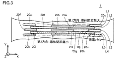
- the elastic conductor 1 includes a stretchable base material 10 having conductivity, and a plurality of conductive members 20a to 20m.
- the stretchable base material 10 is configured to be stretchable.
- the stretchable base material 10 has, for example, a substantially rectangular shape.
- the stretchable base material 10 is, for example, a plan view in which the X-axis direction that is the first direction is the longitudinal direction and the Y-axis direction that is the second direction orthogonal to the first direction is the short direction. It has a rectangular shape.
- the Z-axis direction is the thickness direction of the stretchable substrate 10.
- a material obtained by kneading conductive powder (such as spherical, fibrous or flaky) into a rubber member or a resin can be used.
- a thermoplastic elastomer such as SEBS (styrene / ethylene / butylene / styrene copolymer) added with a carbon filler can be employed.
- NBR nitrile rubber
- CR chloroprene rubber
- EPDM ethylene propylene rubber
- silicone rubber IIR (isobutene / isoprene rubber)
- SBR styrene rubber
- urethane rubber CSM (hypalon), FKM ( Fluorine rubber) or the like
- the rubber member 1) an elastic modulus of about several MPa, 2) a heat resistance of at least 100 ° C., preferably 150 ° C. to 200 ° C., 3) a shape restoring property, 4) a biocompatibility, 5 )
- the properties such as moisture permeability, those having one or more properties are preferred.
- a metal such as Ag, Cu, Al, Zn, Ni, Sn, or an alloy of these two or more metals may be added.
- the plurality of conductive members 20a to 20m have a longitudinal shape extending in the first direction.
- the plurality of conductive members 20a to 20m are disposed on the surface 10a of the stretchable base material.
- the plurality of conductive members 20a to 20m have lower specific resistance and higher elastic modulus than the stretchable base material 10.
- the plurality of conductive members 20a to 20m are made of, for example, metal foil.
- a copper foil can be used as the metal foil.
- the plurality of conductive members 20a to 20m are formed by a subtractive method such as a printing method, a photolithography method, or a direct drawing method.
- the plurality of conductive members 20a to 20m are separated from each other in a second direction perpendicular to the first direction, and at least in a section I extending along the first direction when viewed from the second direction. , And so as to be continuous from one end side to the other end side along the first direction.
- the plurality of conductive members 20a to 20m are arranged in a staggered manner.
- the first line L1 to the fifth line L5 are configured by arranging a part of the plurality of conductive members 20a to 20m apart from each other along the first direction and arranged in a straight line.
- the first line L1 to the fifth line L5 are sequentially spaced apart from each other along the Y-axis direction.
- the third line L3 is located at the center of the stretchable base material 10 in the second direction.
- the first line L1, the third line L3, and the fifth line L5 have substantially the same configuration.
- the first line L1 includes conductive members 20a, 20b, and 20c.
- the conductive members 20a, 20b, and 20c are linearly spaced apart from each other in the first direction.
- the third line L3 includes conductive members 20f, 20g, and 20h.
- the conductive members 20f, 20g, and 20h are linearly spaced apart from each other in the first direction.
- the fifth line L5 includes conductive members 20k, 20l, and 20m.
- the conductive members 20k, 20l, and 20m are linearly spaced apart from each other in the first direction.
- the conductive members 20a, 20f, and 20k are located on one end side of the section I.
- the conductive members 20a, 20f, and 20k have substantially the same length.
- One end of the conductive members 20a, 20f, and 20k in the first direction overlaps when viewed from the second direction.
- the other ends of the conductive members 20a, 20f, and 20k in the first direction overlap when viewed from the second direction.
- the conductive members 20a, 20f, and 20k are spaced apart from each other in the second direction.
- the conductive members 20c, 20h, and 20m are located on the other end side of the section I.
- the conductive members 20c, 20h, and 20m have substantially the same length.
- One end of the conductive members 20c, 20h, and 20m in the first direction overlaps when viewed from the second direction.
- the other ends of the conductive members 20c, 20h, and 20m in the first direction overlap when viewed from the second direction.
- the conductive members 20c, 20h, and 20m are spaced apart in the second direction.
- the conductive members 20b, 20g, and 20l are positioned between the conductive members 20a, 20f, and 20k and the conductive members 20c, 20h, and 20m in the first direction.
- the conductive members 20b, 20g, and 20l have substantially the same length.
- One end of the conductive members 20b, 20g, and 20l in the first direction overlaps when viewed from the second direction.
- the other ends of the conductive members 20b, 20g, 20l in the first direction overlap when viewed from the second direction.
- the conductive members 20b, 20g, and 20l are spaced apart in the second direction.
- the second line L2 and the fourth line L4 have substantially the same configuration.
- the second line L2 includes conductive members 20d and 20e.
- the second line L2 is located between the first line L1 and the third line L3 in the second direction.
- the fourth line L4 is located between the third line L3 and the fifth line L5 in the second direction.
- the conductive members 20d and 20e are linearly spaced apart from each other in the first direction.
- One end side of the conductive member 20d in the first direction is located between the conductive members 20a and 20f in the second direction.
- One end of the conductive member 20d in the first direction is located inside the one end of the conductive members 20a and 20f in the first direction. That is, one end of the conductive member 20d in the first direction is positioned on the other end side of the conductive members 20a and 20f in the first direction with respect to one end of the conductive members 20a and 20f in the first direction.
- the other end side of the conductive member 20d in the first direction is located between the conductive members 20b and 20g in the second direction.
- the other end of the conductive member 20d in the first direction is located closer to one end side of the conductive members 20b and 20g in the first direction than the central part of the conductive members 20b and 20g.
- the one end side of the conductive member 20e in the first direction is located between the conductive members 20b and 20g in the second direction.
- One end of the conductive member 20e in the first direction is located on the other end side in the first direction of the conductive members 20b and 20g with respect to the central part of the conductive members 20b and 20g.
- the other end side of the conductive member 20e in the first direction is located between the conductive members 20c and 20h in the second direction.
- the other end of the conductive member 20e in the first direction is located inside the other ends of the conductive members 20c and 20h in the first direction. That is, the other end of the conductive member 20e in the first direction is located closer to one end side of the conductive members 20c and 20h in the first direction than the other end of the conductive members 20c and 20h in the first direction.
- the conductive members 20i and 20j are linearly spaced apart from each other in the first direction.
- One end side of the conductive member 20i in the first direction is located between the conductive members 20f and 20k in the second direction.
- One end of the conductive member 20i in the first direction is located inside the one end of the conductive members 20f and 20k in the first direction. That is, one end of the conductive member 20i in the first direction is located on the other end side of the conductive members 20f and 20k in the first direction with respect to one end of the conductive members 20f and 20k in the first direction.
- the other end side of the conductive member 20i in the first direction is located between the conductive members 20g and 20l in the second direction.
- the other end of the conductive member 20i in the first direction is located on one end side of the conductive members 20g, 20l in the first direction with respect to the central part of the conductive members 20g, 20l.
- the one end side in the first direction of the conductive member 20j is located between the conductive members 20g and 20l in the second direction.
- One end of the conductive member 20j in the first direction is located on the other end side of the conductive members 20g, 20l in the first direction with respect to the central part of the conductive members 20g, 20l.
- the other end side of the conductive member 20j in the first direction is located between the conductive members 20h and 20m in the second direction.
- the other end of the conductive member 20j in the first direction is located inside the other end of the conductive members 20h and 20m in the first direction. That is, the other end of the conductive member 20j in the first direction is positioned closer to one end side of the conductive members 20h and 20m in the first direction than the other end of the conductive members 20h and 20m in the first direction.
- the elastic base material 10 having a low elastic modulus has a plurality of high elastic modulus.
- the elastic base material 10 having a low elastic modulus has a plurality of high elastic modulus.
- the distance between the conductive members 20a and 20b and the distance between the conductive members 20b and 20c in the first direction are increased.
- 20 l and the distance between the conductive members 20 l, 20 m become longer.
- the distance between the conductive members 20a, 20b and the conductive member 20d and the distance between the conductive members 20b, 20c and the conductive member 20e in the second direction are shorter than those in the first state.
- the distance between the conductive member 20d and the conductive members 20f and 20g and the distance between the conductive member 20e and the conductive members 20g and 20h in the second direction are shorter than in the first state.
- the distance between the conductive members 20k and 20l and the conductive member 20i and the distance between the conductive members 20l and 20m and the conductive member 20j are shorter than in the first state
- the distance between the conductive member 20i and the conductive members 20f and 20g and the distance between the conductive member 20j and the conductive members 20g and 20h in the second direction are shorter than in the first state.
- a conductive path is formed, for example, as indicated by a dashed arrow.
- the stretchable base material 10 When the stretchable base material 10 extends in the first direction, the width of the stretchable base material 10 in the second direction becomes small, and the electrical resistance of the stretchable base material 10 in the stretch direction is reduced in the portion where the width becomes small.
- the elastic conductor 1 since the increase in the electric resistance of the stretchable base material 10 is considerably offset by forming the conductive path as described above, the elastic conductor 1 is elastic. It can suppress that the whole electrical resistance of the conductor 1 increases.
- an increase in electrical resistance accompanying an increase in path length can be suppressed when the elastic conductor 1 is extended in a predetermined direction.
- FIG. 4 to 8 are cross-sectional views showing the first to fifth steps of the method of manufacturing the elastic conductor according to the present embodiment.
- FIG. 4 to FIG. 8 a method for manufacturing the elastic conductor 1 according to the present embodiment will be described.
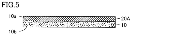
- the stretchable base material 10 and the conductive member precursor 20A are prepared.
- the stretchable substrate 10 for example, a material obtained by adding a carbon filler to SEBS as described above is used.
- the conductive member precursor 20A for example, a sheet-like copper foil having a roughened main surface 20A1 on one side is used.
- the stretchable base material 10 and the conductive member precursor so that the roughened main surface 20 ⁇ / b> A ⁇ b> 1 faces the stretchable base material 10.
- Thermocompression bonding is performed at a temperature of about 120 ° C. to 180 ° C. with 20A facing each other.
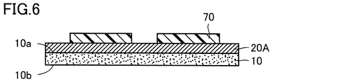
- a photoresist is applied, and a resist pattern 70 is formed by exposure and development.
- the resist pattern 70 has a shape corresponding to a plurality of conductive members.
- the material, film thickness, and formation method of the photoresist are arbitrary, and the photoresist may be a positive type or a negative type.
- the conductive member precursor 20A is etched using an etchant, and the plurality of conductive members 20a to 20m are made into the stretchable substrate 10.
- the etching solution for example, a ferric chloride solution is used.
- the elastic conductor 1 is manufactured by removing the resist pattern 70 in the fifth step of the method of manufacturing the elastic conductor 1.
- FIG. 9 is a plan view of the elastic conductor according to the present embodiment. With reference to FIG. 9, the elastic conductor 1A according to the present embodiment will be described.
- the elastic conductor 1 ⁇ / b> A has a plurality of conductive member pattern shapes and electrode portions 21 and 22 when compared with the elastic conductor 1 according to the first embodiment. It differs in the point provided.
- the plurality of conductive members 20a1 and 20b1 are separated from each other in a second direction perpendicular to the first direction, and at least in a section I extending along the first direction when viewed from the second direction. , And so as to be continuous from one end side to the other end side along the first direction.
- at least a part of the section I is, for example, between the electrode portions 21 and 22 provided on one end side and the other end side in the first direction of the stretchable base material 10.
- One end of the conductive member 20a1 in the first direction is connected to an electrode portion 21 provided on one end side of the stretchable base material 10 in the first direction.
- the other end side in the first direction of the conductive member 20a1 is opposed to one end side in the first direction of the conductive member 20b1 in the second direction.
- the other end of the conductive member 20a1 in the first direction is located on the other end side of the conductive member 20b1 in the first direction with respect to one end of the conductive member 20b1 in the first direction.
- the one end side of the conductive member 20b1 in the first direction opposes the other end side of the conductive member 20a in the first direction in the second direction.
- the other end of the conductive member 20b1 is connected to the electrode portion 22 provided on the other end side of the stretchable base material 10 in the first direction.
- the electrode portions 21 and 22 have a substantially rectangular shape in which the first direction is the short direction and the second direction is the long direction.
- the electrode parts 21 and 22 are electrically connected to a wiring member or the like.
- the elastic base material 10 having a low elastic modulus has the elastic modulus.
- the conductivity along the second direction is compared with the first state in which no tensile force acts in the first direction.
- the interval between the sex members 20a1 and 20b1 is shortened.
- a conductive path is formed so as to pass through the conductive members 20a1 and 20b1 close to each other as in the first embodiment.
- the stretchable base material 10 By forming the conductive path, the stretchable base material 10 extends in the first direction and the width in the second direction decreases, thereby increasing the electrical resistance of the stretchable base material 10 in the first direction. Even in this case, the increase in the electric resistance of the stretchable base material 10 is offset to a considerable extent. Thereby, it can suppress that the whole electrical resistance of the elastic conductor 1 increases. As a result, even in the elastic conductor 1A according to the present embodiment, an increase in electrical resistance associated with an increase in path length can be suppressed when the elastic conductor 1A is extended in a predetermined direction.
- FIG. 10 is a plan view of the elastic conductor according to the present embodiment.
- the elastic conductor 1B according to the present embodiment will be described with reference to FIG.
- the pattern shape of the plurality of conductive members and the electrode portions 21 and 22 are The difference is provided.
- the plurality of conductive members 20a2 to 20g2 are separated from each other in a second direction perpendicular to the first direction, and when viewed from the second direction, at least in a section I extending along the first direction. , And so as to be continuous from one end side to the other end side along the first direction.
- the plurality of conductive members 20a2 to 20g2 are arranged in a staggered manner.
- a part of the plurality of conductive members 20a2 to 20g2 is arranged in a straight line apart from each other along the first direction, thereby forming the first line L1 to the third line L3.
- the first line L1 to the third line L3 are sequentially spaced apart from each other along the Y-axis direction.
- the 2nd line L2 is located in the center part in the 2nd direction of the elastic base material 10.
- the first line L1 and the third line L3 have substantially the same configuration.
- the first line L1 includes conductive members 20a2 and 20b2.
- the conductive members 20a2 and 20b2 are linearly spaced apart from each other in the first direction.
- the third line L3 includes conductive members 20f2 and 20g2.
- the conductive members 20f2 and 20g2 are linearly spaced apart from each other in the first direction.
- the conductive members 20a2 and 20f2 are located on one end side of the section I.
- the conductive members 20a2 and 20f2 have substantially the same length.
- One end of the conductive members 20a2 and 20f2 in the first direction overlaps when viewed from the second direction.
- the other ends of the conductive members 20a2 and 20f2 in the first direction overlap when viewed from the second direction.
- the conductive members 20a2 and 20f2 are disposed apart from each other in the second direction.
- the conductive members 20b2 and 20g2 are located on one end side of the section I.
- the conductive members 20b2 and 20g2 have substantially the same length.
- One end of the conductive members 20b2 and 20g2 in the first direction overlaps when viewed from the second direction.
- the other ends of the conductive members 20b2 and 20g2 in the first direction overlap when viewed from the second direction.
- the conductive members 20b2 and 20g2 are spaced apart in the second direction.
- the second line L2 includes conductive members 20c2, 20d2, and 20e2.
- the conductive members 20c2, 20d2, and 20e2 are linearly spaced apart from each other in the first direction.
- One end of the conductive member 20c2 in the first direction is connected to the electrode portion 21.
- the other end side of the conductive member 20c2 in the first direction is located between the conductive members 20a2 and 20f2 in the second direction.
- the other end of the conductive member 20a2 in the first direction is positioned closer to one end of the conductive members 20a2 and 20f2 than the central part of the conductive members 20a2 and 20f2.
- One end side of the conductive member 20d2 is located between the conductive members 20a2 and 20f2 in the second direction.
- One end of the conductive member 20d2 is located on the other end side of the conductive members 20a2 and 20f2 with respect to the central portion of the conductive members 20a2 and 20f2.
- the other end side of the conductive member 20d2 is located between the conductive members 20b2 and 20g2 in the second direction.
- the other end of the conductive member 20d2 is located on one end side in the first direction of the conductive members 20b2 and 20g2 with respect to the central portion of the conductive members 20b2 and 20g2.
- the one end side of the conductive member 20e2 is located between the conductive members 20b2 and 20g2.
- One end of the conductive member 20e2 is located on the other end side in the first direction of the conductive members 20b2 and 20g2 with respect to the central portion of the conductive members 20b2 and 20g2.
- the other end of the conductive member 20 e 2 is connected to the electrode portion 22.
- the elastic base material 10 having a low elastic modulus has the elastic modulus.
- the conductive material along the first direction is compared with the first state in which no tensile force acts in the first direction. The interval between the conductive members becomes longer and the interval between the conductive members along the second direction becomes shorter.
- the interval between the conductive members 20a2 and 20b2 in the first direction is shortened.
- the distance between the conductive members 20c2 and 20d2 and the distance between the conductive members 20d2 and 20e2 in the first direction are shortened.
- the interval between the conductive members 20f2 and 20g2 in the first direction is shortened.
- the 1st line L1 and the 3rd line L3 approach the 2nd line L2 located in the center part in the 2nd direction of elastic substrate 10.
- the distance between the conductive member 20a2 and the conductive members 20c2 and 20d2 and the distance between the conductive member 20b2 and the conductive members 20d2 and 20e2 are shortened, and the conductivity in the second direction is reduced.
- the distance between the conductive members 20c2 and 20d2 and the conductive member 20f2 and the distance between the conductive members 20d2 and 20e2 and the conductive member 20g2 are shortened.
- a conductive path is formed so that a current passes through the conductive members 20c2, 20a2, 20d2, 20b2, and 20e2 in the proximity state, and the conductive members 20c2, 20f2, 20d2, 20g2, and 20e2 in the proximity state are formed.
- a conductive path is formed to allow current to pass.
- the stretchable base material 10 By forming the conductive path, the stretchable base material 10 extends in the first direction and the width in the second direction decreases, thereby increasing the electrical resistance of the stretchable base material 10 in the first direction. Even in this case, the increase in the electric resistance of the stretchable base material 10 is offset to a considerable extent. Thereby, it can suppress that the whole electrical resistance of the elastic conductor 1 increases. As a result, even in the elastic conductor 1B according to the present embodiment, an increase in electrical resistance accompanying an increase in path length can be suppressed when the elastic conductor 1B is extended in a predetermined direction.
- the elastic conductor 1B according to the present embodiment since the number of conductive paths is increased as compared with the elastic conductor 1A according to the second embodiment, the overall electrical resistance of the elastic conductor 1 is increased. This can be further suppressed.
- FIG. 11 is a plan view of the elastic conductor according to the present embodiment. An elastic conductor 1C according to the present embodiment will be described with reference to FIG.
- the elastic conductor 1C according to the present embodiment is provided with electrode portions 21A to 21C and 22A to 22C when compared with the elastic conductor 1 according to the first embodiment. Is different.
- the electrode portions 21A, 21B, and 21C are provided apart from each other in the second direction.
- the electrode portions 22A, 22B, and 22C are provided apart from each other in the second direction.
- At least one of the electrode portions 21A, 21B, and 21C is electrically connected to a wiring member or the like. At least one of the electrode portions 22A, 22B, and 22C is electrically connected to a wiring member or the like.
- the electrode portions 21A to 21C and 22A to 22C apart from each other in the second direction, the electrode portions 21A to 21C are brought close to each other when the stretchable base material 10 extends in the first direction.
- the electrode portions 22A to 22C can be brought close to each other.
- the integral electrode is formed when the stretchable base material 10 extends in the first direction. In the vicinity of each part, the shrinkage
- the electrode parts 21A to 21C are brought close to each other, and the electrode parts 22A to 22C are brought close to each other, whereby the conductive member 20a connected to the electrode part 21A is made conductive as a whole. While being able to move toward the member 20f, the conductive member 20c connected to the electrode portion 22A can be moved toward the conductive member 20h as a whole.
- the conductive member 20k connected to the electrode portion 21C can be moved toward the conductive member 20i as a whole, and the conductive member 20m connected to the electrode portion 22C can be moved as a whole to the conductive member 20j. Can be moved toward.
- the above-described conductive path can be reliably formed.
- the stretchable base material 10 extends in the first direction and the width in the second direction decreases, thereby increasing the electrical resistance of the stretchable base material 10 in the first direction.
- the increase in the electric resistance of the stretchable base material 10 is offset to a considerable extent. Thereby, it can suppress that the whole electrical resistance of the elastic conductor 1 increases.
- an increase in electrical resistance associated with an increase in path length can be suppressed when the elastic conductor 1C is extended in a predetermined direction.
- the number of lines in the second direction is larger than that of the elastic conductor 1B according to the third embodiment, and therefore the number of conductive paths formed in the second state is smaller. To increase. Thereby, in elastic conductor 1C according to the present embodiment, it is possible to further suppress an increase in the overall electrical resistance of elastic conductor 1 as compared with elastic conductor 1B according to the third embodiment.
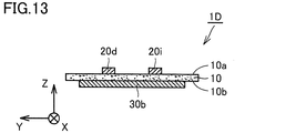
- FIG. 12 is a plan view of the elastic conductor according to the present embodiment.
- 13 is a cross-sectional view taken along line XIII-XIII shown in FIG.
- FIG. 14 is a diagram illustrating a state in which the elastic conductor according to the present embodiment is pulled along the first direction.
- the elastic conductor 1D according to the present embodiment will be described with reference to FIGS.
- the elastic conductor 1D according to the present embodiment is provided with restraining members 30a to 30d when compared with the elastic conductor 1 according to the first embodiment. Is different.
- a part of the plurality of conductive members 20a to 20m is arranged along the second direction, so that the stretchable base material 10 extends along the second direction.
- a dense region where the number of conductive members per width is dense and a sparse region where the number of conductive members per width along the second direction of the stretchable base material 10 is smaller than the dense region are formed.
- the restraining members 30a to 30d are provided on the back surface 10b of the stretchable base material 10 on the side opposite to the front surface 10a of the stretchable base material 10 on which the plurality of conductive members 20a to 20m are provided.
- Constraint members 30a to 30d have an elastic modulus higher than the elastic modulus of the stretchable base material 10, and suppress the stretch of the stretchable base material 10 in the second direction.
- the restraining members 30a to 30d are configured to include a portion extending in the second direction.
- the restraining members 30a to 30d have, for example, a longitudinal shape extending in the second direction.
- the shapes of the restraining members 30a to 30d are not limited to the longitudinal shape, and can be changed as appropriate.
- the restraining members 30a to 30d are provided on the back surface 10b of the stretchable base material 10 so as to overlap the sparse region when viewed from the normal direction of the surface 10a of the stretchable base material 10.
- the restraining members 30a to 30d are made of, for example, a metal foil.
- the restraining members 30a to 30d may be composed of the same members as the conductive members 20a to 20m, or may be composed of different members. Further, the restraining members 30a to 30d do not have to be conductors, and may be made of a highly elastic resin member such as polyimide.
- the second direction is compared with the first state.
- the distance between the conductive members along the line is shortened, and a conductive path is formed.
- the elastic conductor 1E according to the present embodiment is obtained by thermocompression bonding a metal foil as a conductive member precursor and a metal foil as a restraining member precursor to the front surface 10a and the back surface 10b of the stretchable base material 10 It can be manufactured by patterning the conductive member precursor and the constraining member precursor using the photolithography method as in the first mode.
- the conductive member precursor, the constraining member precursor, and the stretchable base material 10 may be provided with through holes that penetrate in the thickness direction at the same position.
- each through hole provided in the conductive member precursor, the restraining member precursor, and the stretchable base material 10 communicates, that is, each through hole is used for a positioning mark.
- the conductive member precursor, the constraining member precursor, and the stretchable base material 10 are overlapped and thermocompression bonded, thereby preventing displacement of the conductive member precursor and the constraining member precursor, and the conductive member precursor accurately.
- the restraining member precursor can be fixed to the stretchable substrate 10. In addition, you may fix to a through-hole through a positioning pin as needed.
- the conductive member precursor and the constraining member precursor can be patterned with high accuracy, and the plurality of conductive members 20a to 20m and the constraining members 30a to 30d can be formed with high accuracy.
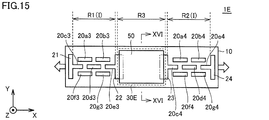
- FIG. 15 is a plan view of the elastic conductor according to the present embodiment.
- FIG. 15 is a diagram illustrating a state before the elastic conductor is pulled along the first direction.
- 16 is a cross-sectional view taken along the line XVI-XVI shown in FIG.
- FIG. 17 is a diagram showing a state where the elastic conductor according to the present embodiment is pulled along the first direction.
- the elastic conductor 1 ⁇ / b> E is an electronic component on the surface of the stretchable base material 10 when compared with the elastic conductor 1 according to the first embodiment.
- the circuit board 50 is provided, and is different in that a restraining member 30E is provided on the back surface of the stretchable base material 10 in the portion where the circuit board 50 is provided.
- the electronic component illustrated the circuit board 50 it is not limited to this, Surface mount components, such as a capacitor
- the plurality of conductive members are provided in the first region R1 and the second region R2.
- the first region R1 and the second region R2 constitute at least a section I of the stretchable base material 10 extending along the first direction.
- the first region R1 and the second region R2 are spaced apart in the second direction.
- An electronic component mounting region R3 for mounting electronic components is provided on the surface of the stretchable base material 10 located between the first region and the second region R2.
- the plurality of conductive members 20a3 to 20g3 are provided in the first region R1.
- the plurality of conductive members 20a3 to 20g3 have substantially the same arrangement relationship as the plurality of conductive members 20a2 to 20g2 according to the third embodiment.
- One end of the conductive member 20c3 in the first direction is connected to the electrode portion 21.
- the other end of the conductive member 20e3 in the first direction is connected to the electrode portion 22.
- the plurality of conductive members 20a4 to 20g4 are provided in the first region R1.
- the plurality of conductive members 20a4 to 20g4 have substantially the same arrangement relationship as the plurality of conductive members 20a2 to 20g2 according to the third embodiment.
- One end of the conductive member 20c4 in the first direction is connected to the electrode portion 23.
- the other end of the conductive member 20e3 in the first direction is connected to the electrode unit 24.
- the circuit board 50 has terminal portions on both ends in the first direction.
- the terminal part of the circuit board 50 is connected to the electrode part 22 and the electrode part 23 by solder or the like.
- a region between one end of the electrode unit 22 in the first direction and the other end of the electrode unit 23 in the first direction corresponds to the electronic component mounting region R3.
- the restraining member 30E is provided on the back surface 10b of the stretchable base material 10 so as to overlap the electronic component mounting region R3 when viewed from the normal direction of the surface 10a of the stretchable base material 10.
- the restraining member 30 ⁇ / b> E has a higher elastic modulus than the elastic modulus of the stretchable base material 10, and suppresses the stretch of the stretchable base material 10 in the second direction.
- Constraint member 30E has, for example, a rectangular shape.
- the shape of the restraining member 30E is not limited to a rectangular shape as long as the expansion and contraction of the stretchable base material 10 in the second direction can be suppressed, and may be a polygonal shape, a circular shape, a frame shape, a lattice shape, or the like. Good.
- the restraining member 30E may be composed of the same member as the plurality of conductive members 20a3 to 20g3, 20a4 to 20g4, or may be composed of different members. Further, the restraining member 30E does not need to be a conductor, and may be configured by a highly elastic resin member such as polyimide or epoxy resin. In the case where the restraining member 30E is made of a highly elastic resin member, an adhesive or the like may be used to adhere the stretchable base material and the restraining member.
- the first region R1 and the second region R2 have a plurality of conductive properties. While the members 20a3 to 20g3 and the plurality of conductive members 20a4 to 20g4 are close to each other in the second direction, expansion / contraction of the stretchable base material 10 in the second direction at a portion corresponding to the electronic component mounting region R3 can be suppressed. . In addition, the restraining member 30E can suppress not only expansion / contraction of the stretchable base material 10 in the second direction but also expansion / contraction in any direction.
- the second direction is compared with the first state.
- the distance between the conductive members along the line is shortened, and a conductive path is formed.
- the elastic conductor 1E according to the present embodiment can be manufactured in accordance with the method for manufacturing the elastic conductor 1D according to the fifth embodiment.
- the circuit board 50 is fixed to the electrode portions 22 and 23 with solder or the like after the plurality of conductive members and the restraining member 30E are formed.
- the elastic conductor 1E according to the present embodiment has been described by exemplifying the case where the first region R1, the second region R2, and the electronic component mounting region R3 are formed.
- the configuration may be such that the second region R2 is not provided and the first region R1 and the electronic component mounting region R3 are provided. In this case, it is preferable that the electronic component mounting region R3 is provided adjacent to the first region R1. Even in the case of such a configuration, the same effect as described above can be obtained.
- the restraining member 30E has the back surface 10b of the stretchable base material 10 so as to overlap the electronic component mounting region R3 when viewed from the normal direction of the front surface 10a of the stretchable base material 10.
- the present invention is not limited to this and may be provided inside the stretchable base material 10.
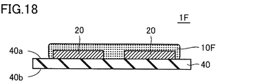
- FIG. 18 is a plan view of the elastic conductor according to the present embodiment.
- the elastic conductor 1F according to the present embodiment will be described with reference to FIG.
- the elastic conductor 1F according to the present embodiment has a plurality of conductive members 20 and a stretchable base material having conductivity when compared with the elastic conductor 1 according to the first embodiment. 10F and the elastic base material 40 which supports them, and the difference is that a plurality of conductive members 20 are provided inside the elastic base material 10F.
- the elastic substrate 40 has a plate shape.
- the elastic base material 40 has a first main surface 40a and a second main surface 40b that face opposite to each other.
- the elastic base material 40 is configured to be stretchable.
- the elastic substrate 40 is made of a thermoplastic elastomer such as SEBS.
- the plurality of conductive members 20 are provided on the first main surface 40 a of the elastic base material 40.
- the plurality of conductive members 20 have substantially the same configuration as that of the first embodiment, for example.
- the plurality of conductive members 20 have an elastic modulus higher than the elastic modulus of the elastic substrate 40 and the elastic modulus of the stretchable substrate 10F.
- the plurality of conductive members 20 are made of, for example, a single-phase metal foil such as Cu, Ag, Au, Ni, Zn, Al, Sn, or a metal foil made of an alloy including at least a part thereof.
- the material of the metal foil is not particularly limited, but a specific resistance of 10 ⁇ 5 ⁇ ⁇ m or less is preferable.
- the material of the metal foil is preferably a metal mainly composed of Cu in consideration of versatility and cost.
- the surface of the plurality of conductive members 20 may be subjected to surface treatment such as NiAu plating or NiPdAu plating.
- the plurality of conductive members 20 may be formed by a subtractive method, an additive method using plating growth, or a method of transferring a pre-patterned metal foil.
- the stretchable base material 10 ⁇ / b> F is provided on the first main surface 40 a of the elastic base material 40 so as to cover the plurality of conductive members 20.
- the stretchable base material 10F has conductivity and is configured to be stretchable.
- the stretchable base material 10F may be a conductive material having stretchability, and is a highly conductive material represented by polyacetylene, polyphenylene, polyphenylene vinylene, polypyrrole, polythiophene, PEDOT (polyethylenedioxythiophene), polyaniline, polyacene, graphene and the like.
- a kneaded molecule or resin and a one-dimensional conductor typified by Ag nanowire or carbon nanotube, or a conductive rubber kneaded with carbon or metal filler in a thermoplastic elastomer may be used.
- the stretchable substrate 10F may be obtained by kneading a spherical or flat metal filler with a stretchable resin member.
- the metal filler Ag, Cu, Al, Ni, Sn, Zn, or an alloy of these two or more metals can be used.
- the second direction is along the second direction compared to the first state.
- the distance between the conductive members is shortened, and a conductive path is formed.
- the increase in the electric resistance of the stretchable base material 10 expressed in the second state is offset to a considerable extent, and thus the overall electric resistance of the elastic conductor 1 is increased. This can be suppressed.
- the elastic conductor 1F according to the present embodiment can suppress an increase in electrical resistance accompanying an increase in the path length when the elastic conductor 1F is extended in a predetermined direction.
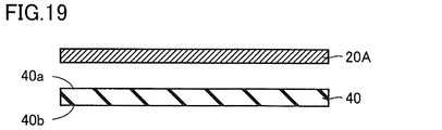
- FIG. 19 to FIG. 24 are views showing steps 1 to 6 of the method of manufacturing the elastic conductor according to the present embodiment. With reference to FIGS. 19 to 24, a method of manufacturing the elastic conductor according to the present embodiment will be described.
- the elastic base material 40 and the conductive member precursor 20A are prepared.
- the elastic substrate 40 sheet-like SEBS is used.
- the conductive member precursor 20A for example, a sheet-like copper foil having a roughened main surface 20A1 on one side is used.
- the stretchable base material 10 and the conductive member precursor 20A so that the roughened main surface 20A1 faces the elastic base material 40. And thermocompression bonding at a temperature of about 120 ° C. to 180 ° C.
- a photoresist is applied, and a resist pattern 70 is formed by exposure and development.
- the resist pattern 70 has a shape corresponding to a plurality of conductive members.
- the material, film thickness, and formation method of the photoresist are arbitrary, and the photoresist may be a positive type or a negative type.
- the conductive member precursor 20A is etched using an etching solution, so that the plurality of conductive members 20a to 20m are formed on the elastic substrate 40. It forms on the 1st main surface 40a.
- etching solution for example, a ferric chloride solution is used.
- the plurality of conductive members 20 are formed by removing the resist pattern 70.
- the first main surface 40a of the elastic base 40 is covered with a conductive paste mainly composed of Ag filler so as to cover the plurality of conductive members 20. Apply on top. Subsequently, the applied conductive paste is dried in an environment of 80 ° C. to 150 ° C. to form a stretchable base material 10F having stretchability and conductivity. Thereby, the elastic conductor 1F is manufactured.
- the elastic conductor corresponding to the elastic conductor according to Embodiments 1 to 6 can be manufactured based on the method of manufacturing the elastic conductor 1F according to the present embodiment.
- the elastic conductor corresponding to the elastic conductor according to the first to sixth embodiments forms a pattern shape equivalent to the plurality of conductive members according to the first to sixth embodiments on the elastic base material, and expands and contracts them. Covered with a conductive substrate.
- the elastic conductor corresponding to the fifth embodiment includes a restraining member that has a higher elastic modulus than the elastic base material 40 and restrains the expansion and contraction of the elastic base material 40 in the second direction, and corresponds to the fifth embodiment.
- a plurality of conductive members are arranged along the second direction, so that the number of conductive members per width along the second direction of the stretchable base material is dense.
- the main surface 40a is provided on the second main surface so as to overlap the sparse region.
- the elastic conductor corresponding to the sixth embodiment includes a restraining member that has a higher elastic modulus than the elastic base material 40 and suppresses the elastic base material 40 from extending in the second direction, and corresponds to the sixth embodiment.
- An electronic component mounting area for mounting an electronic component is provided on the surface of the stretchable base material adjacent to at least a part of the section I. When the restraining member is viewed from the normal direction of the second main surface, It is provided on the second main surface or inside the elastic base material 40 so as to overlap the electronic component mounting region.
- FIG. 25 is a diagram showing the conditions and results of a verification experiment performed to verify the effects of the present invention. With reference to FIG. 25, the condition and result of the verification experiment performed in order to verify the effect of this invention are demonstrated.
- the vertical axis represents the resistance of the elastic conductor
- the horizontal axis represents the elongation of the elastic conductor in the first direction.
- the elastic conductor in Comparative Example 1 and the elastic conductors according to Examples 1 to 3 were prepared.
- the elastic conductor in Comparative Example 1 a material in which a plurality of conductive members were not provided and electrodes were provided on both ends of a stretchable base material having stretchability and conductivity was used.
- the elastic conductor according to Example 1 the elastic conductor according to Embodiment 2 was used.
- the elastic body according to Embodiment 3 was used.
- the elastic conductor according to Embodiment 4 was used.
- the conductive path formed in the second state in the order of the first embodiment, the second embodiment, and the third embodiment. The number is increasing.
- the change in resistance was measured when the elastic conductor in Comparative Example 1 and the elastic conductors according to Examples 1 to 3 were extended in the first direction.
- the electrical resistance of the 1st state of the elastic conductor in the comparative example 1 and the elastic conductor which concerns on Examples 1-3 was made to become the same value.
- Example 1 in the state of 11% elongation, the value was approximately 1.5 times that of the first state. Further, when the elongation exceeded 11%, the rate of increase in electrical resistance increased, but was reduced compared to Comparative Example 1.
- Example 2 in the state of 11% elongation, the value was about 1.4 times that of the first state. Further, when the elongation exceeded 11%, the rate of increase in electrical resistance increased, but was reduced compared to Comparative Example 1.
- Example 3 in the state of 11% elongation, the value was approximately 1.2 times that of the first state. Further, when the elongation exceeded 11%, the rate of increase in electrical resistance increased, but was reduced compared to Comparative Example 1.
- the number of conductive paths formed when pulled in the first direction is different, and the formation is performed in the order of Example 1, Example 2, and Example 3.
- the number of conductive paths to be performed is increasing. Since the increase rate of the electrical resistance decreases in the order of Example 1, Example 2, and Example 3, the increase in the electrical resistance when the conductive path is increased further in the first direction is further increased. It can be said that it was confirmed experimentally that it can be suppressed.
- (First use example) 26 and 27 are views showing a first state and a second state of the first usage example of the elastic conductor according to the present invention.
- the elastic conductor 1 connects a sensor unit 110 provided on a human fingertip and a control board 130 fixed to a wristband 120 wound around a wrist. .
- the detection result detected from the sensor unit 110 is input to the control unit provided on the control board 130 via the elastic conductor 1.
- the sensor unit 110 is provided so as to be able to detect body temperature, for example.
- the tensile force in the first direction is not applied to the elastic conductor 1 when the fingertip is extended.
- a tensile force acts in the first direction at the bent portion. Thereby, the elastic conductor 1 extends in the first direction.
- the interval between the conductive members along the second direction is shortened, and a conductive path is formed.
- the increase in electrical resistance accompanying the increase in path length can be suppressed, and when the body temperature is detected by the sensor unit 110 as described above, the body temperature can be detected stably.
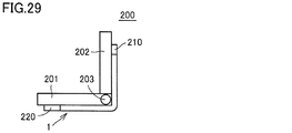
- (Second usage example) 28 and 29 are views showing a first state and a second state of the second usage example of the elastic conductor according to the present invention.
- the elastic conductor 1 connects the sensor unit 210 provided on the distal end side of the movable arm unit 202 and the control board 220 provided on the fixed arm unit 201. To do.
- the detection result detected from the sensor unit 210 is input to the control unit provided on the control board 220 via the elastic conductor 1.
- the movable arm portion 202 is fixed to the fixed arm portion 201 by a hinge mechanism 203.
- the movable arm unit 202 is configured to be rotatable around the rotation axis with the direction perpendicular to the paper surface as the rotation axis.
- the sensor unit 210 is provided so as to be able to detect, for example, temperature and humidity.
- FIG. 28 when the movable arm portion 202 and the fixed arm portion 201 are arranged in a straight line, the elastic conductor 1 is not subjected to a tensile force in the first direction.
- FIG. 27 when the movable arm unit 202 rotates around the rotation axis, a tensile force acts in the first direction that is the extending direction of the elastic conductor 1. Thereby, the elastic conductor 1 extends in the first direction.
- the interval between the conductive members along the second direction is shortened, and a conductive path is formed.
- an increase in electrical resistance accompanying an increase in path length can be suppressed, and when the sensor unit 210 detects temperature, humidity, etc., as described above, the temperature, humidity, etc. are stably detected. be able to.
- the electroconductive member was comprised by metal foil
- the bulk metal material refers to a bulk metal material in which a metal is solidified, and does not include a metal material formed by drying a binder including a large number of metal particles such as a paste material. is there.
Landscapes
- Engineering & Computer Science (AREA)
- Microelectronics & Electronic Packaging (AREA)
- Structure Of Printed Boards (AREA)
- Insulated Conductors (AREA)
- Non-Insulated Conductors (AREA)
- Electrophotography Configuration And Component (AREA)
Abstract
弾性導電体(1)は、第1状態と第1状態から第1方向に伸長した第2状態とを切り換え可能に構成されたものであって、伸縮性基材(10)と、長手形状を有し、伸縮性基材(10)の表面に配置され、伸縮性基材(10)よりも比抵抗が低く弾性率が高い複数の導電性部材(20a~20m)とを備え、第1状態において、複数の導電性部材(20a~20m)は、第1方向と垂直な第2方向に互いに離間しつつ、第2方向から見た場合に、第1方向に沿って延在する区間において一端側から他端側にかけて連なるように設けられ、第2状態における第2方向に互いに隣り合う導電性部材(20a~20m)間の距離が、第1状態における第2方向に互い隣り合う導電性部材(20a~20m)間の距離よりも短くなっている。
Description
本発明は、第1方向に引張力が作用する前の第1状態と、上記第1方向に引張力が作用し、上記第1方向に伸長した第2状態とを切り換え可能に構成された弾性導電体に関する。
伸縮可能に構成された弾性導電体が開示された文献として、特開2005-322492号公報(特許文献1)が挙げられる。特許文献1に開示の弾性導電体においては、粒子状または繊維状の磁性導電体をゴム状弾性体に混練し、磁場により所定の第1方向に配向させつつ、一部の磁性導電体を第1方向に交差する第2方向に分岐させる。
このように構成することにより、第1方向に配向する磁性体導電体間を、第2方向に分岐した磁性導電体によって接続させることができ、電気抵抗を低くすることができるとともに、良好な導通を有することとされている。
しかしながら、特許文献1に構成においては、金属粒子が配向する第1方向に相当程度伸長させた場合には、第1方向に配向する粒子状または繊維状の磁性導電体間の接続が分断される。この場合には、弾性導電体の電気抵抗が増加することが懸念される。
本発明は、上記のような問題に鑑みてなされたものであり、本発明の目的は、所定の方向に伸長させた場合に、経路長の増大に伴う電気抵抗の増加を抑制することができる弾性導電体を提供することにある。
本発明に基づく弾性導電体は、第1方向に引張力が作用する前の第1状態と、上記第1方向に引張力が作用し、上記第1方向に伸長した第2状態とを切り換え可能に構成された弾性導電体であって、導電性を有する伸縮性基材と、上記第1方向に延在する長手形状を有し、上記伸縮性基材の表面または内部に配置され、上記伸縮性基材よりも比抵抗が低く、弾性率が高い複数の導電性部材と、を備え、上記第1状態において、上記複数の導電性部材は、上記第1方向と垂直な第2方向に互いに離間しつつ、上記第2方向から見た場合に、上記第1方向に沿って延在する少なくとも一部の区間において上記第1方向に沿って一端側から他端側にかけて連なるように設けられ、上記第2状態における上記第2方向に互いに隣り合う上記導電性部材間の距離が、上記第1状態における上記第2方向に互いに隣り合う上記導電性部材間の距離よりも短くなっている。
上記本発明に基づく弾性導電体にあっては、上記導電性部材は、バルク状の金属材料または金属箔によって構成されていることが好ましい。ここで、バルク状の金属材料とは、金属が固化した塊状の金属材料を示しており、ペースト材料等の多数の金属粒を含むバインダが乾燥することにより形成される金属材料を含まないものである。
上記本発明に基づく弾性導電体は、上記伸縮性基材の弾性率よりも高い弾性率を有し、上記伸縮性基材の上記第2方向への伸縮を抑制する拘束部材をさらに備えていてもよい。この場合には、上記少なくとも一部の区間には、上記複数の導電性部材の一部が上記第2方向に沿って並ぶことにより、上記伸縮性基材の上記第2方向に沿った幅あたりの上記導電性部材の本数が密となる密領域と、上記密領域よりも上記伸縮性基材の上記第2方向に沿った幅あたりの上記導電性部材の本数が疎となる疎領域とが形成されることが好ましい。また、上記拘束部材は、上記伸縮性基材の上記表面の法線方向から見た場合に、上記疎領域に重なるように、上記伸縮性基材の裏面もしくは内部に設けられていることが好ましい。
上記本発明に基づく弾性導電体は、上記伸縮性基材の弾性率よりも高い弾性率を有し、上記伸縮性基材の上記第2方向への伸縮を抑制する拘束部材をさらに備えていてもよい。この場合には、上記少なくとも一部の区間に隣接する上記伸縮性基材の上記表面には、電子部品を搭載する電子部品搭載領域が設けられていてもよい。また、上記拘束部材は、上記伸縮性基材の上記表面の法線方向から見た場合に、上記電子部品搭載領域に重なるように、上記伸縮性基材の裏面に設けられていることが好ましい。
上記本発明に基づく弾性導電体は、互いに反対側を向く第1主面および第2主面を有し、上記伸縮性基材および上記複数の導電性部材を支持する弾性基材をさらに備えていてもよい。この場合には、上記導電性部材は、上記第1主面上に設けられることが好ましく、上記伸縮性基材は、上記複数の導電性部材を覆うように上記第1主面上に設けられていることが好ましい。
上記本発明に基づく弾性導電体は、上記弾性基材よりも弾性率が高く上記弾性基材の上記第2方向への伸縮を拘束する拘束部材をさらに備えていてもよい。この場合には、上記少なくとも一部の区間には、上記複数の導電性部材の一部が上記第2方向に沿って並ぶことにより、上記伸縮性基材の上記第2方向に沿った幅あたりの上記導電性部材の本数が密となる密領域と、上記密領域よりも上記伸縮性基材の上記第2方向に沿った幅あたりの上記導電性部材の本数が疎となる疎領域とが形成されることが好ましい。また、上記拘束部材は、上記第2主面の法線方向から見た場合に、上記疎領域に重なるように、上記第2主面上に設けられていることが好ましい。
上記本発明に基づく弾性導電体は、上記弾性基材よりも弾性率が高く、上記弾性基材の上記第2方向への伸びを抑制する拘束部材をさらに備えていてもよい。この場合には、上記少なくとも一部の区間に隣接する上記伸縮性基材の上記表面には、電子部品を搭載する電子部品搭載領域が設けられることが好ましい。また、上記拘束部材は、上記第2主面の法線方向から見た場合に、上記電子部品搭載領域に重なるように、上記第2主面上に設けられていることが好ましい。
本発明によれば、所定の方向に伸長させた場合に、経路長の増大に伴う電気抵抗の増加を抑制することができる弾性導電体を提供することができる。
以下、本発明の実施の形態について、図を参照して詳細に説明する。なお、以下に示す実施の形態においては、同一のまたは共通する部分について図中同一の符号を付し、その説明は繰り返さない。
(実施の形態1)
図1は、本実施の形態1に係る弾性導電体の平面図である。図2は、図1に示すII-II線に沿った断面図である。図3は、本実施の形態1に係る弾性導電体を第1方向に沿って引張させた状態を示す図である。図1から図3を参照して、本実施の形態に係る弾性導電体1について説明する。
図1は、本実施の形態1に係る弾性導電体の平面図である。図2は、図1に示すII-II線に沿った断面図である。図3は、本実施の形態1に係る弾性導電体を第1方向に沿って引張させた状態を示す図である。図1から図3を参照して、本実施の形態に係る弾性導電体1について説明する。
図1から図3に示すように、本実施の形態に係る弾性導電体1は、第1方向に引張力が作用する前の第1状態と、第1方向に引張力が作用し、第1方向に伸長した第2状態とを切り換え可能に構成されている。図1および図2では、弾性導電体1の第1状態を示しており、図3では、弾性導電体1の第2状態を示している。
図1および図2に示すように、弾性導電体1は、導電性を有する伸縮性基材10、および複数の導電性部材20a~20mを備える。伸縮性基材10は、伸縮可能に構成されている。
伸縮性基材10は、たとえば、略矩形形状を有する。具体的には、伸縮性基材10は、たとえば、第1方向となるX軸方向を長手方向とし、第1方向と直交する第2方向となるY軸方向を短手方向とする平面視略長方形形状を有する。なお、Z軸方向は、伸縮性基材10の厚み方向である。
伸縮性基材10としては、導電性粉末(球状、繊維状あるいはフレーク状等のもの)をゴム部材や樹脂に混練した材料を採用することができる。具体的には、たとえば、SEBS(スチレン・エチレン・ブチレン・スチレン共重合体)等の熱可塑性エストラマーにカーボンフィラーを添加したものを採用することができる。ゴム部材として、NBR(ニトリルゴム)、CR(クロロプレンゴム)、EPDM(エチレンプロピレンゴム)、シリコーンゴム、IIR(イソブチエン・イソプレンゴム)、SBR(スチレンゴム)、ウレタンゴム、CSM(ハイパロン)、FKM(フッ素ゴム)等を用いてもよい。また、ゴム部材としては、1)数MPa程度の弾性率、2)低くとも100℃以上、好ましくは、150℃~200℃以上の耐熱性、3)形状復元性、4)生体親和性、5)透湿性といった特性のうち、1つ以上の特性を有するものが好ましい。また、導電性粉末として、カーボンフィラーの他に、Ag,Cu,Al,Zn,Ni,Sn等の金属あるいはこれら2つ以上の金属の合金を添加してもよい。
複数の導電性部材20a~20mは、第1方向に延在する長手形状を有する。複数の導電性部材20a~20mは、伸縮性基材の表面10a上に配置される。複数の導電性部材20a~20mは、伸縮性基材10よりも比抵抗が低く、弾性率が高い。
複数の導電性部材20a~20mは、たとえば金属箔で構成されている。金属箔としては、たとえば銅箔を採用することができる。複数の導電性部材20a~20mは、印刷法、フォトリソグラフィー法、直接描画法等のサブトラクティブ法によって形成される。
複数の導電性部材20a~20mは、第1方向と垂直な第2方向に互いに離間しつつ、第2方向から見た場合に、第1方向に沿って延在する少なくとも一部の区間Iにおいて、第1方向に沿って一端側から他端側にかけて連なるように設けられている。
複数の導電性部材20a~20mは、千鳥状に配置されている。複数の導電性部材20a~20mのうちの一部が第1方向に沿って互いに離間して直線状に並んで配置されることにより、第1ラインL1~第5ラインL5が構成される。第1ラインL1~第5ラインL5は、Y軸方向に沿って互いに離間して順に並んでいる。第3ラインL3は、伸縮性基材10の第2方向における中央部に位置する。
第1ラインL1、第3ラインL3および第5ラインL5は、ほぼ同様の構成を有する。第1ラインL1は、導電性部材20a,20b,20cを含む。導電性部材20a,20b,20cは、第1方向に互いに離間して直線状に配置されている。第3ラインL3は、導電性部材20f,20g,20hを含む。導電性部材20f,20g,20hは、第1方向に互いに離間して直線状に配置されている。第5ラインL5は、導電性部材20k,20l,20mを含む。導電性部材20k,20l,20mは、第1方向に互いに離間して直線状に配置されている。
導電性部材20a,20f,20kは、上記区間Iの一端側に位置する。導電性部材20a,20f,20kは、ほぼ同じ長さを有する。導電性部材20a,20f,20kの第1方向における一端は、第2方向から見た場合に重なる。導電性部材20a,20f,20kの第1方向における他端は、第2方向から見た場合に重なる。導電性部材20a,20f,20kは、第2方向に離間して配置されている。
導電性部材20c,20h,20mは、上記区間Iの他端側に位置する。導電性部材20c,20h,20mは、ほぼ同じ長さを有する。導電性部材20c,20h,20mの第1方向における一端は、第2方向から見た場合に重なる。導電性部材20c,20h,20mの第1方向における他端は、第2方向から見た場合に重なる。導電性部材20c,20h,20mは、第2方向に離間して配置されている。
導電性部材20b,20g,20lは、第1方向における導電性部材20a,20f,20kと導電性部材20c,20h,20mの間に位置する。導電性部材20b,20g,20lは、ほぼ同じ長さを有する。導電性部材20b,20g,20lの第1方向における一端は、第2方向から見た場合に重なる。導電性部材20b,20g,20lの第1方向における他端は、第2方向から見た場合に重なる。導電性部材20b,20g,20lは、第2方向に離間して配置されている。
第2ラインL2および第4ラインL4は、ほぼ同様の構成を有する。第2ラインL2は、導電性部材20d,20eを含む。第2ラインL2は、第2方向における第1ラインL1および第3ラインL3の間に位置する。第4ラインL4は、第2方向における第3ラインL3および第5ラインL5の間に位置する。
導電性部材20d,20eは、第1方向に互いに離間して直線状に配置されている。導電性部材20dの第1方向の一端側は、第2方向における導電性部材20a,20fの間に位置する。導電性部材20dの第1方向の一端は、導電性部材20a,20fの第1方向の一端よりも内側に位置する。すなわち、導電性部材20dの第1方向の一端は、導電性部材20a,20fの第1方向の一端よりも導電性部材20a,20fの第1方向の他端側に位置する。
導電性部材20dの第1方向の他端側は、第2方向における導電性部材20b,20gの間に位置する。導電性部材20dの第1方向の他端は、導電性部材20b,20gの中央部よりも導電性部材20b,20gの第1方向の一端側に位置する。
導電性部材20eの第1方向の一端側は、第2方向における導電性部材20b,20gの間に位置する。導電性部材20eの第1方向の一端は、導電性部材20b,20gの中央部よりも導電性部材20b,20gの第1方向の他端側に位置する。
導電性部材20eの第1方向の他端側は、第2方向における導電性部材20c,20hの間に位置する。導電性部材20eの第1方向の他端は、導電性部材20c,20hの第1方向の他端よりも内側に位置する。すなわち、導電性部材20eの第1方向の他端は、導電性部材20c,20hの第1方向の他端よりも導電性部材20c,20hの第1方向の一端側に位置する。
導電性部材20i,20jは、第1方向に互いに離間して直線状に配置されている。導電性部材20iの第1方向の一端側は、第2方向における導電性部材20f,20kの間に位置する。導電性部材20iの第1方向の一端は、導電性部材20f,20kの第1方向の一端よりも内側に位置する。すなわち、導電性部材20iの第1方向の一端は、導電性部材20f,20kの第1方向の一端よりも導電性部材20f,20kの第1方向の他端側に位置する。
導電性部材20iの第1方向の他端側は、第2方向における導電性部材20g,20lの間に位置する。導電性部材20iの第1方向の他端は、導電性部材20g,20lの中央部よりも導電性部材20g,20lの第1方向の一端側に位置する。
導電性部材20jの第1方向の一端側は、第2方向における導電性部材20g,20lの間に位置する。導電性部材20jの第1方向の一端は、導電性部材20g,20lの中央部よりも導電性部材20g,20lの第1方向の他端側に位置する。
導電性部材20jの第1方向の他端側は、第2方向における導電性部材20h,20mの間に位置する。導電性部材20jの第1方向の他端は、導電性部材20h,20mの第1方向の他端よりも内側に位置する。すなわち、導電性部材20jの第1方向の他端は、導電性部材20h,20mの第1方向の他端よりも導電性部材20h,20mの第1方向の一端側に位置する。
図3に示すように、第1方向に引張力が作用し、第1方向に弾性導電体1が伸長した第2状態においては、弾性率の低い伸縮性基材10が、弾性率の高い複数の導電性部材20a~20mの変形を抑制しつつ第1方向に延在することにより、第1方向に引張力が作用しない第1状態と比較して、第1方向に沿った導電性部材間の間隔が長くなるとともに、第2方向に沿った導電性部材間の間隔が短くなる。
たとえば、第1ラインL1において、第1方向における、導電性部材20a,20b間の間隔および導電性部材20b,20c間の間隔が長くなる。同様に、第3ラインL3および第5ラインL5において、第1方向における、導電性部材20f,20g間の間隔および導電性部材20g,20h間の間隔、ならびに、第1方向における、導電性部材20k,20l間の間隔および導電性部材20l,20m間の間隔が長くなる。
一方で、第1ラインL1、および第2ラインL2は、伸縮性基材10の第2方向における中央部に位置する第3ラインL3に近づく。同様に、第4ラインL4、および第5ラインL5は、伸縮性基材10の第2方向における中央部に位置する第3ラインL3に近づく。
具体的には、第2方向における、導電性部材20a,20bと導電性部材20dとの間隔および導電性部材20b,20cと導電性部材20eとの間隔が、第1状態と比較して短くなるとともに、第2方向における、導電性部材20dと導電性部材20f,20gとの間隔および導電性部材20eと導電性部材20g,20hとの間隔が、第1状態と比較して短くなる。
同様に、第2方向における、導電性部材20k,20lと導電性部材20iとの間隔および導電性部材20l,20mと導電性部材20jとの間隔が、第1状態と比較して短くなるとともに、第2方向における、導電性部材20iと導電性部材20f,20gとの間隔および導電性部材20jと導電性部材20g,20hとの間隔が、第1状態と比較して短くなる。
このように、複数の導電性部材20a~20mが第2方向に近接することにより、たとえば破線矢印に示すように導電パスが形成される。
伸縮性基材10が第1方向に伸長する場合には、伸縮性基材10の第2方向の幅が小さくなり、幅が小さくなる部分において、伸長方向における伸縮性基材10の電気抵抗が増加する。ここで、本実施の形態に係る弾性導電体1においては、上述のような導電性パスが形成されることにより、上記伸縮性基材10の電気抵抗の増加が相当程度相殺されるため、弾性導電体1の全体的な電気的抵抗が増加することを抑制できる。
以上のように、本実施の形態に係る弾性導電体1にあっては、所定の方向に伸長させた場合に、経路長の増大に伴う電気抵抗の増加を抑制することができる。
図4から図8は、本実施の形態に係る弾性導電体の製造方法の第1工程から第5工程を示す断面図である。図4から図8を参照して、本実施の形態に係る弾性導電体1の製造方法について説明する。
図4に示すように、弾性導電体1の製造方法の第1工程において、伸縮性基材10と導電性部材前駆体20Aとを準備する。伸縮性基材10としては、たとえば上述のようにSEBSにカーボンフィラーを添加したものを用いる。導電性部材前駆体20Aとしては、たとえば片側の主面20A1が粗面化されたシート状の銅箔を用いる。
図5に示すように、弾性導電体1の製造方法の第2工程において、粗面化された主面20A1が伸縮性基材10を向くように、伸縮性基材10と導電性部材前駆体20Aとを対向配置させて、120℃~180℃程度の温度で熱圧着を行なう。
図6に示すように、弾性導電体1の製造方法の第3工程において、フォトレジストを塗布して、露光および現像することによってレジストパターン70を形成する。レジストパターン70は、複数の導電性部材に対応した形状を有する。
フォトレジストの材質、膜厚、形成方法は任意であり、フォトレジストは、ポジ型であってもよいし、ネガ型であってもよい。
図7に示すように、弾性導電体1の製造方法の第4工程において、エッチング液を用いて導電性部材前駆体20Aをエッチングして、複数の導電性部材20a~20mを伸縮性基材10の表面10a上に形成する。エッチング液としては、たとえば、塩化第2鉄溶液を用いる。
図8に示すように、弾性導電体1の製造方法の第5工程において、レジストパターン70を除去することにより、弾性導電体1が製造される。
(実施の形態2)
図9は、本実施の形態に係る弾性導電体の平面図である。図9を参照して、本実施の形態に係る弾性導電体1Aについて説明する。
図9は、本実施の形態に係る弾性導電体の平面図である。図9を参照して、本実施の形態に係る弾性導電体1Aについて説明する。
図9に示すように、本実施の形態に係る弾性導電体1Aは、実施の形態1に係る弾性導電体1と比較した場合に、複数の導電性部材のパターン形状および電極部21,22が設けられている点において相違する。
複数の導電性部材20a1,20b1は、第1方向と垂直な第2方向に互いに離間しつつ、第2方向から見た場合に、第1方向に沿って延在する少なくとも一部の区間Iにおいて、第1方向に沿って一端側から他端側にかけて連なるように設けられている。ここで、少なくとも一部の区間Iとは、たとえば伸縮性基材10の第1方向の一端側および他端側に設けられた電極部21,22の間である。
導電性部材20a1の第1方向の一端は、伸縮性基材10の第1方向の一端側に設けられた電極部21に接続されている。導電性部材20a1の第1方向の他端側は、導電性部材20b1の第1方向の一端側に第2方向において対向する。導電性部材20a1の第1方向の他端は、導電性部材20b1の第1方向の一端よりも導電性部材20b1の第1方向の他端側に位置する。
導電性部材20b1の第1方向の一端側は、導電性部材20aの第1方向の他端側に第2方向において対向する。導電性部材20b1の他端は、伸縮性基材10の第1方向の他端側に設けられた電極部22に接続されている。
電極部21,22は、第1方向を短手方向とし、第2方向を長手方向とする略矩形形状を有する。電極部21,22は、配線部材等に電気的に接続される。
このように構成される場合においても、第1方向に引張力が作用し、第1方向に弾性導電体1が伸長した第2状態においては、弾性率の低い伸縮性基材10が、弾性率の高い複数の導電性部材20a1,20b1の変形を抑制しつつ第1方向に延在することにより、第1方向に引張力が作用しない第1状態と比較して、第2方向に沿った導電性部材20a1,20b1間の間隔が短くなる。
これにより、第2状態においては、実施の形態1同様に互いに近接した導電性部材20a1,20b1を通過するように導電パスが形成される。
導電性パスが形成されることによって、伸縮性基材10が第1方向に伸長して第2方向の幅が小さくなることにより第1方向への伸縮性基材10の電気的抵抗が増加した場合であっても、伸縮性基材10の電気抵抗の増加が相当程度相殺される。これにより、弾性導電体1の全体的な電気的抵抗が増加することを抑制できる。この結果、本実施の形態に係る弾性導電体1Aにあっても、所定の方向に伸長させた場合に、経路長の増大に伴う電気抵抗の増加を抑制することができる。
(実施の形態3)
図10は、本実施の形態に係る弾性導電体の平面図である。図10を参照して、本実施の形態に係る弾性導電体1Bについて説明する。
図10は、本実施の形態に係る弾性導電体の平面図である。図10を参照して、本実施の形態に係る弾性導電体1Bについて説明する。
図10に示すように、本実施の形態に係る弾性導電体1Bは、実施の形態1に係る弾性導電体1と比較した場合に、複数の導電性部材のパターン形状および電極部21,22が設けられている点が相違する。
複数の導電性部材20a2~20g2は、第1方向と垂直な第2方向に互いに離間しつつ、第2方向から見た場合に、第1方向に沿って延在する少なくとも一部の区間Iにおいて、第1方向に沿って一端側から他端側にかけて連なるように設けられている。
複数の導電性部材20a2~20g2は、千鳥状に配置されている。複数の導電性部材20a2~20g2のうちの一部が第1方向に沿って互いに離間して直線状に並んで配置されることにより、第1ラインL1~第3ラインL3が構成される。第1ラインL1~第3ラインL3は、Y軸方向に沿って互いに離間して順に並んでいる。第2ラインL2は、伸縮性基材10の第2方向における中央部に位置する。
第1ラインL1、第3ラインL3は、ほぼ同様の構成を有する。第1ラインL1は、導電性部材20a2,20b2を含む。導電性部材20a2,20b2は、第1方向に互いに離間して直線状に配置されている。第3ラインL3は、導電性部材20f2,20g2を含む。導電性部材20f2,20g2は、第1方向に互いに離間して直線状に配置されている。
導電性部材20a2,20f2は、上記区間Iの一端側に位置する。導電性部材20a2,20f2は、ほぼ同じ長さを有する。導電性部材20a2,20f2の第1方向における一端は、第2方向から見た場合に重なる。導電性部材20a2,20f2の第1方向における他端は、第2方向から見た場合に重なる。導電性部材20a2,20f2は、第2方向に離間して配置されている。
導電性部材20b2,20g2は、上記区間Iの一端側に位置する。導電性部材20b2,20g2は、ほぼ同じ長さを有する。導電性部材20b2,20g2の第1方向における一端は、第2方向から見た場合に重なる。導電性部材20b2,20g2の第1方向における他端は、第2方向から見た場合に重なる。導電性部材20b2,20g2は、第2方向に離間して配置されている。
第2ラインL2は、導電性部材20c2,20d2,20e2を含む。導電性部材20c2,20d2,20e2は、第1方向に互いに離間して直線状に配置されている。
導電性部材20c2の第1方向の一端は、電極部21に接続されている。導電性部材20c2の第1方向の他端側は、第2方向における導電性部材20a2,20f2の間に位置する。導電性部材20a2の第1方向の他端は、導電性部材20a2,20f2の中央部よりも導電性部材20a2,20f2の一端側に位置する。
導電性部材20d2の一端側は、第2方向における導電性部材20a2,20f2の間に位置する。導電性部材20d2の一端は、導電性部材20a2,20f2の中央部よりも導電性部材20a2,20f2の他端側に位置する。
導電性部材20d2の他端側は、第2方向における導電性部材20b2,20g2の間に位置する。導電性部材20d2の他端は、導電性部材20b2,20g2の中央部よりも導電性部材20b2,20g2の第1方向の一端側に位置する。
導電性部材20e2の一端側は、導電性部材20b2,20g2の間に位置する。導電性部材20e2の一端は、導電性部材20b2,20g2の中央部よりも導電性部材20b2,20g2の第1方向の他端側に位置する。導電性部材20e2の他端は、電極部22に接続されている。
このように構成される場合においても、第1方向に引張力が作用し、第1方向に弾性導電体1が伸長した第2状態においては、弾性率の低い伸縮性基材10が、弾性率の高い複数の導電性部材20a2~20g2の変形を抑制しつつ第1方向に延在することにより、第1方向に引張力が作用しない第1状態と比較して、第1方向に沿った導電性部材間の間隔が長くなるとともに、第2方向に沿った導電性部材間の間隔が短くなる。
具体的には、第1ラインL1において、第1方向における、導電性部材20a2,20b2間の間隔が短くなる。第2ラインL2において、第1方向における、導電性部材20c2,20d2の間隔および導電性部材20d2,20e2間の間隔が短くなる。第3ラインL3において、第1方向における、導電性部材20f2,20g2間の間隔が短くなる。
一方で、第1ラインL1および第3ラインL3は、伸縮性基材10の第2方向における中央部に位置する第2ラインL2に近づく。
具体的には、第2方向における、導電性部材20a2と導電性部材20c2,20d2との間隔、導電性部材20b2と導電性部材20d2,20e2との間隔が短くなるとともに、第2方向における、導電性部材20c2,20d2と導電性部材20f2との間隔および導電性部材20d2,20e2と導電性部材20g2との間隔が短くなる。
これにより、近接状態における導電性部材20c2,20a2,20d2,20b2,20e2を電流が通過するように導電性パスが形成されるとともに、近接状態における導電性部材20c2,20f2,20d2,20g2,20e2を電流が通過するように導電性パスが形成される。
導電性パスが形成されることによって、伸縮性基材10が第1方向に伸長して第2方向の幅が小さくなることにより第1方向への伸縮性基材10の電気的抵抗が増加した場合であっても、伸縮性基材10の電気抵抗の増加が相当程度相殺される。これにより、弾性導電体1の全体的な電気的抵抗が増加することを抑制できる。この結果、本実施の形態に係る弾性導電体1Bにあっても、所定の方向に伸長させた場合に、経路長の増大に伴う電気抵抗の増加を抑制することができる。
なお、本実施の形態に係る弾性導電体1Bにおいては、実施の形態2に係る弾性導電体1Aよりも導電パスの本数が増加するため、弾性導電体1の全体的な電気的抵抗が増加することをさらに抑制できる。
(実施の形態4)
図11は、本実施の形態に係る弾性導電体の平面図である。図11を参照して、本実施の形態に係る弾性導電体1Cについて説明する。
図11は、本実施の形態に係る弾性導電体の平面図である。図11を参照して、本実施の形態に係る弾性導電体1Cについて説明する。
図11に示すように、本実施の形態に係る弾性導電体1Cは、実施の形態1に係る弾性導電体1と比較した場合に、電極部21A~21C、22A~22Cが設けられている点において相違する。
電極部21A,21B,21Cは、第2方向に互いに離間して設けられている。電極部22A,22B,22Cは、第2方向に互いに離間して設けられている。
電極部21A,21B,21Cのうち少なくともいずれかは、配線部材等に電気的に接続されている。電極部22A,22B,22Cのうち少なくともいずれかは、配線部材等に電気的に接続されている。
このように電極部21A~21C,22A~22Cが第2方向に離間して設けられることにより、伸縮性基材10が第1方向に伸長した場合に、電極部21A~21Cを互いに近接させることができるとともに、電極部22A~22Cを互いに近接させることができる。
電極部21A~21C,および電極部22A~22Cが、それぞれ離間せずに一体の電極部にて構成される場合には、伸縮性基材10が第1方向に伸長した際に、一体の電極部のそれぞれの近傍においては、第2方向への伸縮性基材10の収縮が抑制される。これにより、導電性部材20aの第1方向の一端側および導電性部材20cの第1方向の他端側が、導電性部材20fおよび導電性部材20hに近づきにくくなる。
ここで、本実施の形態においては、電極部21A~21Cを互いに近接させるとともに、電極部22A~22Cを互いに近接させることにより、電極部21Aに接続される導電性部材20aを全体的に導電性部材20fに向けて移動させることができるとともに、電極部22Aに接続される導電性部材20cを全体的に導電性部材20hに向けて移動させることができる。
また、電極部21Cに接続される導電性部材20kを全体的に導電性部材20iに向けて移動させることができるとともに、電極部22Cに接続される導電性部材20mを全体的に導電性部材20jに向けて移動させることができる。
これにより、伸縮性基材10が第1方向に伸長した第2状態において、上述の導電性パスを確実に形成することができる。導電性パスが形成されることにより、伸縮性基材10が第1方向に伸長して第2方向の幅が小さくなることによって第1方向への伸縮性基材10の電気的抵抗が増加した場合であっても、伸縮性基材10の電気抵抗の増加が相当程度相殺される。これにより、弾性導電体1の全体的な電気的抵抗が増加することを抑制できる。この結果、本実施の形態に係る弾性導電体1Cにあっても、所定の方向に伸長させた場合に、経路長の増大に伴う電気抵抗の増加を抑制することができる。
なお、本実施の形態に係る弾性導電体1Cにおいては、実施の形態3に係る弾性導電体1Bよりも第2方向のライン数が増加するため、第2状態において形成される導電パスの本数が増加する。これにより、本実施の形態に係る弾性導電体1Cにおいては、実施の形態3に係る弾性導電体1Bよりも弾性導電体1の全体的な電気的抵抗が増加することをさらに抑制できる。
(実施の形態5)
図12は、本実施の形態に係る弾性導電体の平面図である。図13は、図12に示すXIII-XIII線に沿った断面図である。図14は、本実施の形態に係る弾性導電体を第1方向に沿って引張させた状態を示す図である。図12から図14を参照して、本実施の形態に係る弾性導電体1Dについて説明する。
図12は、本実施の形態に係る弾性導電体の平面図である。図13は、図12に示すXIII-XIII線に沿った断面図である。図14は、本実施の形態に係る弾性導電体を第1方向に沿って引張させた状態を示す図である。図12から図14を参照して、本実施の形態に係る弾性導電体1Dについて説明する。
図12から図14に示すように、本実施の形態に係る弾性導電体1Dは、実施の形態1に係る弾性導電体1と比較した場合に、拘束部材30a~30dが設けられている点において相違する。
複数の導電性部材20a~20mが設けられる区間Iには、複数の導電性部材20a~20mの一部が第2方向に沿って並ぶことにより、伸縮性基材10の第2方向に沿った幅あたりの導電性部材の本数が密となる密領域と、密領域よりも伸縮性基材10の第2方向に沿った幅あたりの導電性部材の本数が疎となる疎領域とが形成される。
拘束部材30a~30dは、複数の導電性部材20a~20mが設けられている伸縮性基材10の表面10aと反対側にある伸縮性基材10の裏面10bに設けられている。
拘束部材30a~30dは、伸縮性基材10の弾性率よりも高い弾性率を有し、伸縮性基材10の第2方向への伸縮を抑制する。拘束部材30a~30dは、第2方向に延在する部分を含むように構成されている。拘束部材30a~30dは、たとえば第2方向に延在する長手形状を有する。なお、拘束部材30a~30dの形状は、長手形状に限定されず、適宜変更することができる。
拘束部材30a~30dは、伸縮性基材10の表面10aの法線方向から見た場合に、上記疎領域に重なるように、伸縮性基材10の裏面10bに設けられている。拘束部材30a~30dは、たとえば金属箔によって構成される。拘束部材30a~30dは、導電性部材20a~20mと同一の部材によって構成されていてもよいし、異なる部材によって構成されていてもよい。また、拘束部材30a~30dは、導電体である必要はなく、ポリイミド等の高弾性の樹脂部材によって構成されていてもよい。
拘束部材30a~30dを設けることにより、伸縮性基材10を第1方向に伸長させる際に、意図しない方向からも力が作用し、第2方向に伸長するような場合であっても、伸縮性基材10の第2方向への幅の伸長を抑制することができる。
以上のように、本実施の形態においても、第1方向に引張力が作用し、第1方向に弾性導電体1が伸長した第2状態においては、第1状態と比較して、第2方向に沿った導電性部材間の間隔が短くなり、導電性パスが形成される。これにより、第2状態において発現される伸縮性基材10の電気抵抗の増加が、相当程度相殺されるため、弾性導電体1の全体的な電気的抵抗が増加することを抑制できる。この結果、所定の方向に伸長させた場合に、経路長の増大に伴う電気抵抗の増加を抑制することができる。
加えて、拘束部材30a~30dが形成されることにより、上述のように、伸縮性基材10を第1方向に伸長させる際に、意図しない方向からも力が作用し、第2方向に伸長するような場合であっても、伸縮性基材10の第2方向への幅の伸長を抑制することができる。
本実施の形態に係る弾性導電体1Eは、伸縮性基材10の表面10aおよび裏面10bに導電性部材前駆体としての金属箔および拘束部材前駆体としての金属箔を熱圧着して、実施の形態1同様にフォトリソグラフィー法を用いて、導電性部材前駆体および拘束部材前駆体をパターニングすることにより製造することができる。
導電性部材前駆体および拘束部材前駆体をパターニングする際には、両面に金属箔が圧着された伸縮性基板において、一方側の金属箔から他方側の金属箔にかけて厚み方向に貫通する貫通孔を形成し、当該貫通孔を位置合わせマークとして、パターニングすることにより、精度よく、導電性部材および拘束部材を形成することができる。
なお、導電性部材前駆体、拘束部材前駆体および伸縮性基材10は、同じ位置に厚み方向に貫通する貫通孔が設けられているものを準備してもよい。この場合には、たとえば、導電性部材前駆体、拘束部材前駆体および伸縮性基材10に設けられた各貫通孔が連通するように、すなわち、各貫通孔を位置決めマークの用途で用いて、導電性部材前駆体、拘束部材前駆体および伸縮性基材10を重ね合せて熱圧着することにより、導電性部材前駆体および拘束部材前駆体の位置ずれを防止し、精度よく導電性部材前駆体および拘束部材前駆体を伸縮性基材10に固定することができる。なお、必要に応じて貫通孔に位置決めピンを通して固定してもよい。
このことによっても、導電性部材前駆体および拘束部材前駆体を精度よくパターニングでき、複数の導電性部材20a~20mおよび拘束部材30a~30dを精度よく形成することができる。
(実施の形態6)
図15は、本実施の形態に係る弾性導電体の平面図である。図15は、弾性導電体を第1方向に沿って引張させる前の状態を示す図である。図16は、図15に示すXVI-XVI線に沿った断面図である。図17は、本実施の形態に係る弾性導電体を第1方向に沿って引張させた状態を示す図である。図15から図17を参照して、本実施の形態に係る弾性導電体1Eについて説明する。
図15は、本実施の形態に係る弾性導電体の平面図である。図15は、弾性導電体を第1方向に沿って引張させる前の状態を示す図である。図16は、図15に示すXVI-XVI線に沿った断面図である。図17は、本実施の形態に係る弾性導電体を第1方向に沿って引張させた状態を示す図である。図15から図17を参照して、本実施の形態に係る弾性導電体1Eについて説明する。
図15から図17に示すように、本実施の形態に係る弾性導電体1Eは、実施の形態1に係る弾性導電体1と比較した場合に、伸縮性基材10の表面上に電子部品としての回路基板50が設けられており、回路基板50が設けられている部分における伸縮性基材10の裏面に拘束部材30Eが設けられている点において相違する。なお、電子部品が回路基板50を例示したが、これに限定されず、コンデンサ、チップコイルなどの表面実装部品、IC等のバンプを持った素子であってもよい。
複数の導電性部材は、第1領域R1と第2領域R2とに設けられている。第1領域R1と第2領域R2は、第1方向に沿って延在する伸縮性基材10の少なくとも一部の区間Iを構成する。第1領域R1と第2領域R2とは、第2方向に離間して設けられている。第1領域と第2領域R2との間に位置する伸縮性基材10の表面には電子部品を搭載する電子部品搭載領域R3が設けられている。
複数の導電性部材20a3~20g3は、第1領域R1に設けられている。複数の導電性部材20a3~20g3は、実施の形態3に係る複数の導電性部材20a2~20g2とほぼ同様の配置関係にある。
導電性部材20c3の第1方向の一端は、電極部21に接続されている。導電性部材20e3の第1方向の他端は、電極部22に接続されている。
複数の導電性部材20a4~20g4は、第1領域R1に設けられている。複数の導電性部材20a4~20g4は、実施の形態3に係る複数の導電性部材20a2~20g2とほぼ同様の配置関係にある。
導電性部材20c4の第1方向の一端は、電極部23に接続されている。導電性部材20e3の第1方向の他端は、電極部24に接続されている。
回路基板50は、第1方向の両端側に端子部を有する。回路基板50の端子部は、半田等により電極部22と電極部23とに接続されている。電極部22の第1方向の一端と電極部23の第1方向の他端との間の領域が、電子部品搭載領域R3に相当する。
拘束部材30Eは、伸縮性基材10の表面10aの法線方向から見た場合に、電子部品搭載領域R3に重なるように、伸縮性基材10の裏面10bに設けられている。拘束部材30Eは、伸縮性基材10の弾性率よりも高い弾性率を有し、伸縮性基材10の第2方向への伸縮を抑制する。
拘束部材30Eは、たとえば矩形形状を有する。なお、拘束部材30Eの形状は、伸縮性基材10の第2方向への伸縮を抑制できる限り、矩形形状に限定されず、多角形形状、円形状、枠状、格子状等であってもよい。
拘束部材30Eは、複数の導電性部材20a3~20g3,20a4~20g4と同一の部材によって構成されていてもよいし、異なる部材によって構成されていてもよい。また、拘束部材30Eは、導電体である必要はなく、ポリイミドやエポキシ樹脂等の高弾性の樹脂部材によって構成されていてもよい。拘束部材30Eが高弾性の樹脂部材によって構成されている場合には、伸縮性基材と拘束部材との密着性させるために接着剤等を使用してもよい。
このように、拘束部材30Eを設けることにより、図17に示すように、伸縮性基材10が第1方向に伸長される際に、第1領域R1および第2領域R2において、複数の導電性部材20a3~20g3および複数の導電性部材20a4~20g4を第2方向に近接させつつ、電子部品搭載領域R3に対応する部分における伸縮性基材10の第2方向への伸縮を抑制することができる。なお、拘束部材30Eは、伸縮性基材10の第2方向への伸縮のみならず、いずれの方向への伸縮も抑制することができる。
以上のように、本実施の形態においても、第1方向に引張力が作用し、第1方向に弾性導電体1が伸長した第2状態においては、第1状態と比較して、第2方向に沿った導電性部材間の間隔が短くなり、導電性パスが形成される。これにより、第2状態において発現される伸縮性基材10の電気抵抗の増加が、相当程度相殺されるため、弾性導電体1の全体的な電気的抵抗が増加することを抑制できる。この結果、所定の方向に伸長させた場合に、経路長の増大に伴う電気抵抗の増加を抑制することができる。
また、電子部品搭載領域R3に対応する部分における伸縮性基材10の第2方向への幅の伸縮を抑制でき、回路基板50が伸縮性基材10上から離脱することを抑制することができる。
なお、本実施の形態に係る弾性導電体1Eは、実施の形態5に係る弾性導電体1Dの製造方法に準拠して製造することができる。回路基板50は、複数の導電性部材および拘束部材30Eが形成された後に、電極部22,23に半田等によって固定される。
なお、本実施の形態に係る弾性導電体1Eは、第1領域R1、第2領域R2および電子部品搭載領域R3が形成されている場合を例示して説明したが、これに限定されず、第2領域R2が設けられておらず、第1領域R1と電子部品搭載領域R3とが設けられた構成であってもよい。この場合には、電子部品搭載領域R3は、第1領域R1に隣り合うように設けられることが好ましい。このような構成の場合であっても、上記同様の効果が得られる。
また、本実施の形態においては、拘束部材30Eは、伸縮性基材10の表面10aの法線方向から見た場合に、電子部品搭載領域R3に重なるように、伸縮性基材10の裏面10bに設けられている場合を例示して説明したが、これに限定されず、伸縮性基材10の内部に設けられていてもよい。
(実施の形態7)
図18は、本実施の形態に係る弾性導電体の平面図である。図18を参照して、本実施の形態に係る弾性導電体1Fについて説明する。
図18は、本実施の形態に係る弾性導電体の平面図である。図18を参照して、本実施の形態に係る弾性導電体1Fについて説明する。
図18に示すように、本実施の形態に係る弾性導電体1Fは、実施の形態1に係る弾性導電体1と比較した場合に、複数の導電性部材20と導電性を有する伸縮性基材10Fと、それらを支持する弾性基材40とを備え、複数の導電性部材20が伸縮性基材10Fの内部に設けられている点において相違する。
弾性基材40は、板状形状を有する。弾性基材40は、互いに反対側を向く第1主面40aおよび第2主面40bを有する。弾性基材40は、伸縮可能に構成されている。弾性基材40は、たとえばSEBS等の熱可塑性エストラマーによって構成される。
複数の導電性部材20は、弾性基材40の第1主面40a上に設けられている。複数の導電性部材20は、たとえば実施の形態1とほぼ同様の構成を有する。複数の導電性部材20は、弾性基材40の弾性率および伸縮性基材10Fの弾性率よりも高い弾性率を有する。複数の導電性部材20は、たとえばCu,Ag,Au,Ni,Zn,Al,Sn等の単相の金属箔またはこれらの少なくとも一部を含む合金による金属箔によって構成される。
金属箔の材料は、特に限定されないが、比抵抗10-5Ω・m以下が好ましい。金属箔の材料は、汎用性、コスト等を考慮して、Cuを主とする金属が好ましい。酸化防止の目的で、複数の導電性部材20の表面にNiAuメッキやNiPdAuメッキなどの表面処理を行なってもよい。
複数の導電性部材20は、サブトラクティブ法によって形成されてもよいし、メッキ成長等を用いるアディティブ法や予めパターニングされた金属箔を転写する方法によって形成されてもよい。
伸縮性基材10Fは、上記複数の導電性部材20を覆うように弾性基材40の第1主面40a上に設けられている。伸縮性基材10Fは、導電性を有し、伸縮可能に構成されている。伸縮性基材10Fは、伸縮性を有する導電体であればよく、ポリアセチレン、ポリフェニレン、ポリフェニレンビニレン、ポリピロール、ポリチオフェン、PEDOT(ポリエチレンジオキシチオフェン)、ポリアニリン、ポリアセン、グラフェン等に代表される導電性高分子または樹脂と、Agナノワイヤーやカーボンナノチューブに代表される1次元導体とを混練したもの、熱可塑性エストラマーにカーボンや金属フィラーを混練した導電ゴムなどを使用してもよい。また、伸縮性基板10Fは、伸縮可能な樹脂部材に球状あるいは扁平状の金属フィラーを混練したものを使用してもよい。金属フィラーとしては、Ag,Cu,Al,Ni,Sn,Znまたはこれら2つ以上の金属の合金を用いることができる。
このように構成された場合においても、第1方向に引張力が作用し、第1方向に弾性導電体1Fが伸長した第2状態においては、第1状態と比較して、第2方向に沿った導電性部材間の間隔が短くなり、導電性パスが形成される。導電性パスが形成されることにより、第2状態において発現される伸縮性基材10の電気抵抗の増加が、相当程度相殺されるため、弾性導電体1の全体的な電気的抵抗が増加することを抑制できる。この結果、本実施の形態に係る弾性導電体1Fは、所定の方向に伸長させた場合に、経路長の増大に伴う電気抵抗の増加を抑制することができる。
図19から図24は、本実施の形態に係る弾性導電体の製造方法の第1工程から図6工程を示す図である。図19から図24を参照して、本実施の形態に係る弾性導電体の製造方法について説明する。
図19に示すように、弾性導電体1Fの製造方法の第1工程において、弾性基材40と導電性部材前駆体20Aとを準備する。弾性基材40としては、シート状のSEBSを用いる。導電性部材前駆体20Aとしては、たとえば片側の主面20A1が粗面化されたシート状の銅箔を用いる。
図20に示すように、弾性導電体1Fの製造方法の第2工程において、粗面化された主面20A1が弾性基材40を向くように、伸縮性基材10と導電性部材前駆体20Aとを対向配置させて、120℃~180℃程度の温度で熱圧着を行なう。
図21に示すように、弾性導電体1Fの製造方法の第3工程において、フォトレジストを塗布して、露光および現像することによってレジストパターン70を形成する。レジストパターン70は、複数の導電性部材に対応した形状を有する。
フォトレジストの材質、膜厚、形成方法は任意であり、フォトレジストは、ポジ型であってもよいし、ネガ型であってもよい。
図22に示すように、弾性導電体1Fの製造方法の第4工程において、エッチング液を用いて導電性部材前駆体20Aをエッチングして、複数の導電性部材20a~20mを弾性基材40の第1主面40a上に形成する。エッチング液としては、たとえば、塩化第2鉄溶液を用いる。
図23に示すように、弾性導電体1Fの製造方法の第5工程において、レジストパターン70を除去することにより、複数の導電性部材20が形成される。
図24に示すように、弾性導電体1Fの製造方法の第6工程において、Agフィラーを主とした導電性ペーストを複数の導電性部材20を覆うように弾性基材40の第1主面40a上に塗布する。続いて、塗布した導電性ペーストを80℃~150℃の環境下で乾燥させて、伸縮性および導電性を有する伸縮性基材10Fを形成する。これにより、弾性導電体1Fが製造される。
なお、本実施の形態に係る弾性導電体1Fの製造方法に準拠して、実施の形態1から6に係る弾性導電体に対応した弾性導電体を製造することができる。実施の形態1から6に係る弾性導電体に対応した弾性導電体とは、弾性基材上に実施の形態1から6に係る複数の導電性部材と同等のパターン形状を形成し、これらを伸縮性基材で覆ったものである。
たとえば、実施の形態5に対応する弾性導電体は、弾性基材40よりも弾性率が高く弾性基材40の第2方向への伸縮を拘束する拘束部材を備え、実施の形態5に対応する少なくとも一部の区間Iには、複数の導電性部材の一部が第2方向に沿って並ぶことにより、伸縮性基材の第2方向に沿った幅あたりの導電性部材の本数が密となる密領域と、密領域よりも伸縮性基材の第2方向に沿った幅あたりの導電性部材の本数が疎となる疎領域とが形成され、拘束部材は、弾性基材40の第2主面40aの法線方向から見た場合に、疎領域に重なるように、第2主面上に設けられている。
また、実施の形態6に対応する弾性導電体は、弾性基材40よりも弾性率が高く、弾性基材40の第2方向への伸びを抑制する拘束部材を備え、実施の形態6に対応する少なくとも一部の区間Iに隣接する伸縮性基材の表面には、電子部品を搭載する電子部品搭載領域が設けられ、拘束部材は、第2主面の法線方向から見た場合に、電子部品搭載領域に重なるように、第2主面上または弾性基材40の内部に設けられている。
(検証実験)
図25は、本発明の効果を検証するために行なった検証実験の条件および結果を示す図である。図25を参照して、本発明の効果を検証するために行なった検証実験の条件および結果について説明する。図25において、縦軸は、弾性導電体の抵抗を表し、横軸に第1方向への弾性導電体の伸びを表している。
図25は、本発明の効果を検証するために行なった検証実験の条件および結果を示す図である。図25を参照して、本発明の効果を検証するために行なった検証実験の条件および結果について説明する。図25において、縦軸は、弾性導電体の抵抗を表し、横軸に第1方向への弾性導電体の伸びを表している。
図25に示すように、本発明の効果を検証するにあたり、比較例1における弾性導電体、および実施例1から3に係る弾性導電体を準備した。比較例1における弾性導電体として、複数の導電性部材が設けられておらず、伸縮性および導電性を有する伸縮性基材の両端に電極部が設けられたものを用いた。実施例1に係る弾性導電体として、実施の形態2に係る弾性導電体を用いた。実施例2に係る弾性導電体として、実施の形態3に係る弾性体を用いた。実施例3に係る弾性導電体として、実施の形態4に係る弾性導電体を用いた。上述したように、実施の形態2、実施の形態3、実施の形態4に対応して、実施例1、実施例2、実施例3の順に、第2状態にて形成される導電性パスの数は、多くなっている。
これら比較例1における弾性導電体、および実施例1から3に係る弾性導電体を第1方向に伸長させた場合における抵抗の変化を測定した。なお、比較例1における弾性導電体および実施例1から3に係る弾性導電体の第1状態の電気抵抗は、同一の値となるようにした。
比較例1においては、第1方向に伸長するにつれて電気抵抗が増加し、11%伸びた状態においては、第1状態と比較して略2.8倍の値となった。また、11%の伸びを超えると、急激に電気抵抗が増加した。
実施例1から3においては、第1方向に伸長するにつれて電気抵抗は増加しているが、その増加量は、比較例1と比較して低くなった。
実施例1においては、11%伸びた状態においては、第1状態と比較して略1.5倍の値となった。また、11%の伸びを超えると、電気抵抗の増加率は高くなったが、比較例1と比較すると、低減されていた。
実施例2においては、11%伸びた状態においては、第1状態と比較して略1.4倍の値となった。また、11%の伸びを超えると、電気抵抗の増加率は高くなったが、比較例1と比較すると、低減されていた。
実施例3においては、11%伸びた状態においては、第1状態と比較して略1.2倍の値となった。また、11%の伸びを超えると、電気抵抗の増加率は高くなったが、比較例1と比較すると、低減されていた。
以上の結果から、第1方向と垂直な第2方向に互いに離間しつつ、第2方向から見た場合に、第1方向に沿って延在する少なくとも一部の区間において第1方向に沿って一端側から他端側にかけて連なるように複数の導電性部材を伸縮性基材に設け、第2状態における第2方向に互いに隣り合う前記導電性部材間の距離が、第1状態における第2方向に互い隣り合う前導電性部材間の距離よりも短くなっている構成とすることにより、第1方向に伸長した場合の電気抵抗の増加を抑制できることが実験的にも確認されたと言える。
実施例1から3に係る弾性導電体においては、第1方向に引張された際に形成される導電パスの数が異なっており、実施例1、実施例2、実施例3の順で、形成される導電性パスの数が多くなっている。実施例1、実施例2、実施例3の順で電気抵抗の増加率が低減していることから、導電性パスが増加するにつれて、第1方向に伸長させた場合の電気抵抗の増加をさらに抑制できることが実験的にも確認されたと言える。
(第1使用例)
図26および図27は、本発明に係る弾性導電体の第1使用例の第1状態および第2状態を示す図である。
図26および図27は、本発明に係る弾性導電体の第1使用例の第1状態および第2状態を示す図である。
図26および図27に示すように、本発明に係る弾性導電体1は、人の指先に設けられたセンサ部110と手首に巻かれたリストバンド120に固定された制御基板130とを接続する。センサ部110から検知された検知結果は、弾性導電体1を介して制御基板130に設けられた制御部に入力される。
センサ部110は、たとえば体温等を検知可能に設けられている。図26に示すように、指先が伸びた状態においては、弾性導電体1には、第1方向への引張力が作用しないようになっている。図27に示すように、弾性導電体1が沿う指が曲げられた状態においては、曲がり部において第1方向に引張力が作用する。これにより、弾性導電体1が第1方向に伸長する。
このような場合においては、第1状態と比較して、第2方向に沿った導電性部材間の間隔が短くなり、導電性パスが形成される。これにより、経路長の増大に伴う電気抵抗の増加を抑制することができ、上述のようにセンサ部110にて体温を検知する場合には、安定して体温を検知することができる。
(第2使用例)
図28および図29は、本発明に係る弾性導電体の第2使用例の第1状態および第2状態を示す図である。
図28および図29は、本発明に係る弾性導電体の第2使用例の第1状態および第2状態を示す図である。
図28および図29に示すように、本発明に係る弾性導電体1は、可動アーム部202の先端側に設けられたセンサ部210と、固定アーム部201に設けられた制御基板220とを接続する。センサ部210から検知された検知結果は、弾性導電体1を介して制御基板220に設けられた制御部に入力される。
可動アーム部202は、ヒンジ機構203によって固定アーム部201に固定されている。可動アーム部202は、紙面垂直方向を回動軸として、回動軸周りに回動可能に構成されている。
センサ部210は、たとえば温度、湿度等を検知可能に設けられている。図28に示すように、可動アーム部202と固定アーム部201が直線状に配置される場合には、弾性導電体1は、第1方向への引張力が作用しないようになっている。図27に示すように、可動アーム部202が回動軸周りに回動した場合には、弾性導電体1の延在方向である第1方向に引張力が作用する。これにより、弾性導電体1が第1方向に伸長する。
このような場合においては、第1状態と比較して、第2方向に沿った導電性部材間の間隔が短くなり、導電性パスが形成される。これにより、経路長の増大に伴う電気抵抗の増加を抑制することができ、上述のようにセンサ部210にて温度、湿度等を検知する場合には、安定して温度、湿度等を検知することができる。
なお、上述した実施の形態に係る弾性導電体においては、導電性部材が金属箔によって構成されている場合を例示して説明したが、これに限定されず、バルク状の金属材料によって構成されていてもよい。ここで、バルク状の金属材料とは、金属が固化した塊状の金属材料を示しており、ペースト材料等の多数の金属粒を含むバインダが乾燥することにより形成される金属材料を含まないものである。
以上、本発明の実施の形態および実施例について説明したが、今回開示された実施の形態および実施例はすべての点で例示であって制限的なものではない。本発明の範囲は請求の範囲によって示され、請求の範囲と均等の意味および範囲内でのすべての変更が含まれる。
1,1A,1B,1C,1D,1E,1F 弾性導電体、10,10F 伸縮性基材、10a 表面、10b 裏面、20,20a,20a1,20a2,20a3,20a4,20b,20b1,20b2,20c,20c2,20c3,20c4,20d,20d2,20e,20e2,20e3,20f,20f2,20g,20g2,20g3,20g4,20h,20i,20j,20k,20l,20m 導電性部材、20A 導電性部材前駆体、20A1 主面、21,21A,21B,21C,22,22A,22B,22C,23,24 電極部、30,30E,30a,30d 拘束部材、40 弾性基材、40a 第1主面、40b 第2主面、50 回路基板、70 レジストパターン、110 センサ部、120 リストバンド、130 制御基板、201 固定アーム部、202 可動アーム部、203 ヒンジ機構、210 センサ部、220 制御基板。
Claims (7)
- 第1方向に引張力が作用する前の第1状態と、前記第1方向に引張力が作用し、前記第1方向に伸長した第2状態とを切り換え可能に構成された弾性導電体であって、
導電性を有する伸縮性基材と、
前記第1方向に延在する長手形状を有し、前記伸縮性基材の表面または内部に配置され、前記伸縮性基材よりも比抵抗が低く、弾性率が高い複数の導電性部材と、を備え、
前記第1状態において、前記複数の導電性部材は、前記第1方向と垂直な第2方向に互いに離間しつつ、前記第2方向から見た場合に、前記第1方向に沿って延在する少なくとも一部の区間において前記第1方向に沿って一端側から他端側にかけて連なるように設けられ、
前記第2状態における前記第2方向に互いに隣り合う前記導電性部材間の距離が、前記第1状態における前記第2方向に互いに隣り合う前記導電性部材間の距離よりも短くなっている、弾性導電体。 - 前記導電性部材は、バルク状の金属材料または金属箔によって構成されている、請求項1に記載の弾性導電体。
- 前記伸縮性基材の弾性率よりも高い弾性率を有し、前記伸縮性基材の前記第2方向への伸縮を抑制する拘束部材をさらに備え、
前記少なくとも一部の区間には、前記複数の導電性部材の一部が前記第2方向に沿って並ぶことにより、前記伸縮性基材の前記第2方向に沿った幅あたりの前記導電性部材の本数が密となる密領域と、前記密領域よりも前記伸縮性基材の前記第2方向に沿った幅あたりの前記導電性部材の本数が疎となる疎領域とが形成され、
前記拘束部材は、前記伸縮性基材の前記表面の法線方向から見た場合に、前記疎領域に重なるように、前記伸縮性基材の裏面に設けられている、請求項1または2に記載の弾性導電体。 - 前記伸縮性基材の弾性率よりも高い弾性率を有し、前記伸縮性基材の前記第2方向への伸縮を抑制する拘束部材をさらに備え、
前記少なくとも一部の区間に隣接する前記伸縮性基材の前記表面には、電子部品を搭載する電子部品搭載領域が設けられ、
前記拘束部材は、前記伸縮性基材の前記表面の法線方向から見た場合に、前記電子部品搭載領域に重なるように、前記伸縮性基材の裏面もしくは内部に設けられている、請求項1から3のいずれか1項に記載の弾性導電体。 - 互いに反対側を向く第1主面および第2主面を有し、前記伸縮性基材および前記複数の導電性部材を支持する弾性基材をさらに備え、
前記導電性部材は、前記第1主面上に設けられ、
前記伸縮性基材は、前記複数の導電性部材を覆うように前記第1主面上に設けられている、請求項1または2に記載の弾性導電体。 - 前記弾性基材よりも弾性率が高く前記弾性基材の前記第2方向への伸縮を拘束する拘束部材をさらに備え、
前記少なくとも一部の区間には、前記複数の導電性部材の一部が前記第2方向に沿って並ぶことにより、前記伸縮性基材の前記第2方向に沿った幅あたりの前記導電性部材の本数が密となる密領域と、前記密領域よりも前記伸縮性基材の前記第2方向に沿った幅あたりの前記導電性部材の本数が疎となる疎領域とが形成され、
前記拘束部材は、前記第2主面の法線方向から見た場合に、前記疎領域に重なるように、前記第2主面上に設けられている、請求項5に記載の弾性導電体。 - 前記弾性基材よりも弾性率が高く、前記弾性基材の前記第2方向への伸びを抑制する拘束部材をさらに備え、
前記少なくとも一部の区間に隣接する前記伸縮性基材の前記表面には、電子部品を搭載する電子部品搭載領域が設けられ、
前記拘束部材は、前記第2主面の法線方向から見た場合に、前記電子部品搭載領域に重なるように設けられている、請求項5または6に記載の弾性導電体。
Priority Applications (4)
| Application Number | Priority Date | Filing Date | Title |
|---|---|---|---|
| EP16836943.7A EP3306621B1 (en) | 2015-08-20 | 2016-07-27 | Elastic conductor |
| CN201680043797.0A CN107851490B (zh) | 2015-08-20 | 2016-07-27 | 弹性导电体 |
| JP2017535306A JP6264512B2 (ja) | 2015-08-20 | 2016-07-27 | 弾性導電体 |
| US15/893,737 US10111325B2 (en) | 2015-08-20 | 2018-02-12 | Elastic conductor |
Applications Claiming Priority (2)
| Application Number | Priority Date | Filing Date | Title |
|---|---|---|---|
| JP2015162721 | 2015-08-20 | ||
| JP2015-162721 | 2015-08-20 |
Related Child Applications (1)
| Application Number | Title | Priority Date | Filing Date |
|---|---|---|---|
| US15/893,737 Continuation US10111325B2 (en) | 2015-08-20 | 2018-02-12 | Elastic conductor |
Publications (1)
| Publication Number | Publication Date |
|---|---|
| WO2017029952A1 true WO2017029952A1 (ja) | 2017-02-23 |
Family
ID=58052157
Family Applications (1)
| Application Number | Title | Priority Date | Filing Date |
|---|---|---|---|
| PCT/JP2016/071972 Ceased WO2017029952A1 (ja) | 2015-08-20 | 2016-07-27 | 弾性導電体 |
Country Status (5)
| Country | Link |
|---|---|
| US (1) | US10111325B2 (ja) |
| EP (1) | EP3306621B1 (ja) |
| JP (1) | JP6264512B2 (ja) |
| CN (1) | CN107851490B (ja) |
| WO (1) | WO2017029952A1 (ja) |
Cited By (1)
| Publication number | Priority date | Publication date | Assignee | Title |
|---|---|---|---|---|
| CN114420343A (zh) * | 2022-01-20 | 2022-04-29 | 广东腐蚀科学与技术创新研究院 | 一种导电材料及接地材料 |
Families Citing this family (3)
| Publication number | Priority date | Publication date | Assignee | Title |
|---|---|---|---|---|
| CN112654498A (zh) * | 2018-11-06 | 2021-04-13 | 积水保力马科技株式会社 | 伸缩配线构件 |
| CN113539554A (zh) * | 2020-04-21 | 2021-10-22 | 深圳市柔宇科技有限公司 | 弹性导线、可拉伸电子产品及弹性导线的制备方法 |
| TWI759828B (zh) * | 2020-08-20 | 2022-04-01 | 友達光電股份有限公司 | 可伸縮電子裝置 |
Citations (3)
| Publication number | Priority date | Publication date | Assignee | Title |
|---|---|---|---|---|
| JP2005259609A (ja) * | 2004-03-12 | 2005-09-22 | Auto Network Gijutsu Kenkyusho:Kk | 電気接続構造および該電気接続構造を備えた自動車用電気接続箱 |
| JP2008058286A (ja) * | 2006-08-31 | 2008-03-13 | Shuichi Ikeda | 摺動型接触子 |
| JP2011070821A (ja) * | 2009-09-24 | 2011-04-07 | Panasonic Electric Works Co Ltd | 透明異方導電性フィルム |
Family Cites Families (7)
| Publication number | Priority date | Publication date | Assignee | Title |
|---|---|---|---|---|
| US7491892B2 (en) * | 2003-03-28 | 2009-02-17 | Princeton University | Stretchable and elastic interconnects |
| JP2005322492A (ja) | 2004-05-07 | 2005-11-17 | Polymatech Co Ltd | 導電弾性体及びその製造方法 |
| US8969724B2 (en) * | 2008-06-25 | 2015-03-03 | Asahi Kasei Fibers Corporation | Elastic signal transmission cable |
| JP5318840B2 (ja) * | 2010-11-08 | 2013-10-16 | デクセリアルズ株式会社 | 異方性導電フィルム、異方性導電フィルムの製造方法、電子部材間の接続方法及び接続構造体 |
| US9767937B2 (en) * | 2012-02-16 | 2017-09-19 | David L. Carnahan | Conductive elastic composite |
| EP2845726A1 (en) | 2013-09-04 | 2015-03-11 | Nederlandse Organisatie voor toegepast -natuurwetenschappelijk onderzoek TNO | Electrically interconnecting foil |
| US10032538B2 (en) * | 2013-11-13 | 2018-07-24 | The United States Of America As Represented By The Secretary Of The Army | Deformable elastomeric conductors and differential electronic signal transmission |
-
2016
- 2016-07-27 WO PCT/JP2016/071972 patent/WO2017029952A1/ja not_active Ceased
- 2016-07-27 CN CN201680043797.0A patent/CN107851490B/zh active Active
- 2016-07-27 JP JP2017535306A patent/JP6264512B2/ja active Active
- 2016-07-27 EP EP16836943.7A patent/EP3306621B1/en active Active
-
2018
- 2018-02-12 US US15/893,737 patent/US10111325B2/en active Active
Patent Citations (3)
| Publication number | Priority date | Publication date | Assignee | Title |
|---|---|---|---|---|
| JP2005259609A (ja) * | 2004-03-12 | 2005-09-22 | Auto Network Gijutsu Kenkyusho:Kk | 電気接続構造および該電気接続構造を備えた自動車用電気接続箱 |
| JP2008058286A (ja) * | 2006-08-31 | 2008-03-13 | Shuichi Ikeda | 摺動型接触子 |
| JP2011070821A (ja) * | 2009-09-24 | 2011-04-07 | Panasonic Electric Works Co Ltd | 透明異方導電性フィルム |
Non-Patent Citations (1)
| Title |
|---|
| See also references of EP3306621A4 * |
Cited By (1)
| Publication number | Priority date | Publication date | Assignee | Title |
|---|---|---|---|---|
| CN114420343A (zh) * | 2022-01-20 | 2022-04-29 | 广东腐蚀科学与技术创新研究院 | 一种导电材料及接地材料 |
Also Published As
| Publication number | Publication date |
|---|---|
| JP6264512B2 (ja) | 2018-01-24 |
| US10111325B2 (en) | 2018-10-23 |
| CN107851490A (zh) | 2018-03-27 |
| US20180168028A1 (en) | 2018-06-14 |
| EP3306621A4 (en) | 2018-06-27 |
| EP3306621A1 (en) | 2018-04-11 |
| CN107851490B (zh) | 2019-08-20 |
| JPWO2017029952A1 (ja) | 2018-02-01 |
| EP3306621B1 (en) | 2020-01-29 |
Similar Documents
| Publication | Publication Date | Title |
|---|---|---|
| JP6574576B2 (ja) | 伸縮性配線基板 | |
| JP6264512B2 (ja) | 弾性導電体 | |
| JP5823879B2 (ja) | フレキシブル回路基板 | |
| US8993893B2 (en) | Multilayer substrate | |
| US9743532B2 (en) | Flexible printed circuit board and manufacturing method of flexible printed circuit board | |
| JP5240827B2 (ja) | フレキシブル配線基板、及び電子機器 | |
| US10575399B2 (en) | Multilayer substrate | |
| JP6331130B2 (ja) | 伸縮性フレキシブル基板およびその製造方法 | |
| CN103514996B (zh) | 复合式软性电路排线 | |
| US10254902B2 (en) | Touch sensor device including a polymer layer having conductive and non-conductive regions | |
| JP2019216273A (ja) | フレキシブル基板 | |
| JP2016040793A (ja) | 伸縮性フレキシブルプリント基板および伸縮性フレキシブルプリント基板の製造方法 | |
| TW201406229A (zh) | 印刷電路板及應用其之製造方法 | |
| CN205092150U (zh) | 柔性电缆以及电子设备 | |
| US20180317324A1 (en) | Electronic component module, dc-dc converter, and electronic device | |
| US9865559B2 (en) | Method for manufacturing stretchable wire and method for manufacturing stretchable integrated circuit | |
| KR20140142936A (ko) | 연성회로기판 및 그 제조방법 | |
| WO2018199084A1 (ja) | 配線基板およびその製造方法 | |
| JP6890015B2 (ja) | 伸縮性配線基板、制御装置および電子機器 | |
| JP6745065B2 (ja) | 電子デバイス | |
| JP2008021676A (ja) | 配線回路基板 |
Legal Events
| Date | Code | Title | Description |
|---|---|---|---|
| 121 | Ep: the epo has been informed by wipo that ep was designated in this application |
Ref document number: 16836943 Country of ref document: EP Kind code of ref document: A1 |
|
| ENP | Entry into the national phase |
Ref document number: 2017535306 Country of ref document: JP Kind code of ref document: A |
|
| NENP | Non-entry into the national phase |
Ref country code: DE |
|
| WWE | Wipo information: entry into national phase |
Ref document number: 2016836943 Country of ref document: EP |